Embed Size (px)
Citation preview
Microelectronic Circuits, Kyung Hee Univ. Spring, 2016
1
1.6 Frequency Response of Amplifiers
• Input signal = sum of sinusoidal signals
• Important its response to input sinusoids of different frequencies
• Amplifier frequency response
Microelectronic Circuits, Kyung Hee Univ. Spring, 2016
2
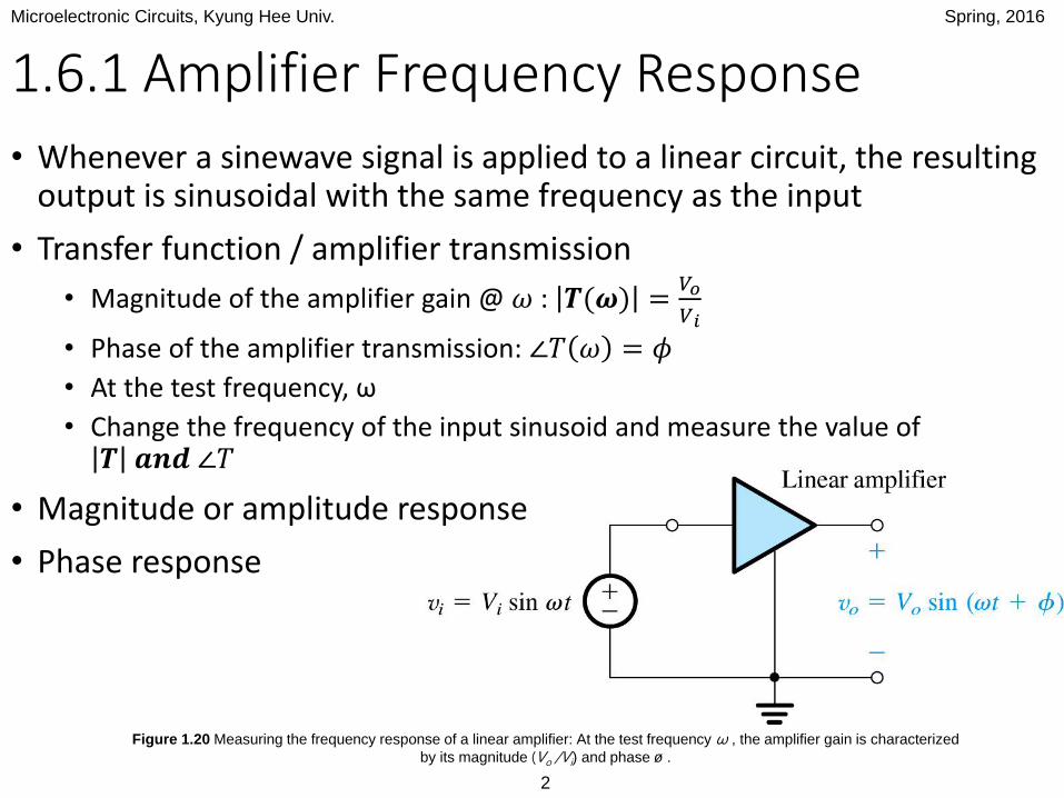
1.6.1 Amplifier Frequency Response
• Whenever a sinewave signal is applied to a linear circuit, the resulting output is sinusoidal with the same frequency as the input
• Transfer function / amplifier transmission
• Magnitude of the amplifier gain @ 𝜔 : 𝑻(𝝎) =𝑉𝑜
𝑉𝑖
• Phase of the amplifier transmission: ∠𝑇 𝜔 = 𝜙
• At the test frequency, ω
• Change the frequency of the input sinusoid and measure the value of 𝑻 𝒂𝒏𝒅 ∠𝑇
• Magnitude or amplitude response
• Phase response
Figure 1.20 Measuring the frequency response of a linear amplifier: At the test frequency ω , the amplifier gain is characterized
by its magnitude (Vo /Vi) and phase ø .
Microelectronic Circuits, Kyung Hee Univ. Spring, 2016
3
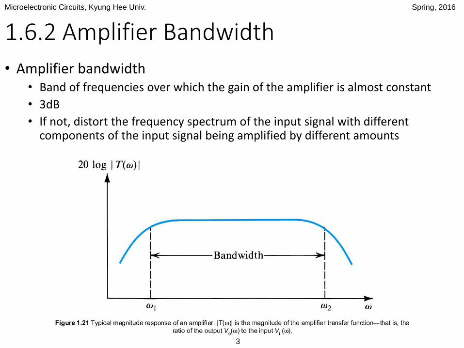
1.6.2 Amplifier Bandwidth
• Amplifier bandwidth• Band of frequencies over which the gain of the amplifier is almost constant
• 3dB
• If not, distort the frequency spectrum of the input signal with different components of the input signal being amplified by different amounts
Microelectronic Circuits, Kyung Hee Univ. Spring, 2016
4
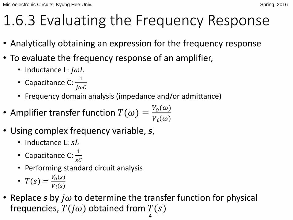
1.6.3 Evaluating the Frequency Response
• Analytically obtaining an expression for the frequency response
• To evaluate the frequency response of an amplifier,• Inductance L: 𝑗𝜔𝐿
• Capacitance C: 1
𝑗𝜔𝐶
• Frequency domain analysis (impedance and/or admittance)
• Amplifier transfer function 𝑇(𝜔) =𝑉𝑜(𝜔)
𝑉𝑖(𝜔)
• Using complex frequency variable, s,• Inductance L: 𝑠𝐿
• Capacitance C: 1
𝑠𝐶
• Performing standard circuit analysis
• 𝑇(𝑠) =𝑉𝑜(𝑠)
𝑉𝑖(𝑠)
• Replace s by 𝑗𝜔 to determine the transfer function for physical frequencies, 𝑇(𝑗𝜔) obtained from 𝑇(𝑠)
Microelectronic Circuits, Kyung Hee Univ. Spring, 2016
5
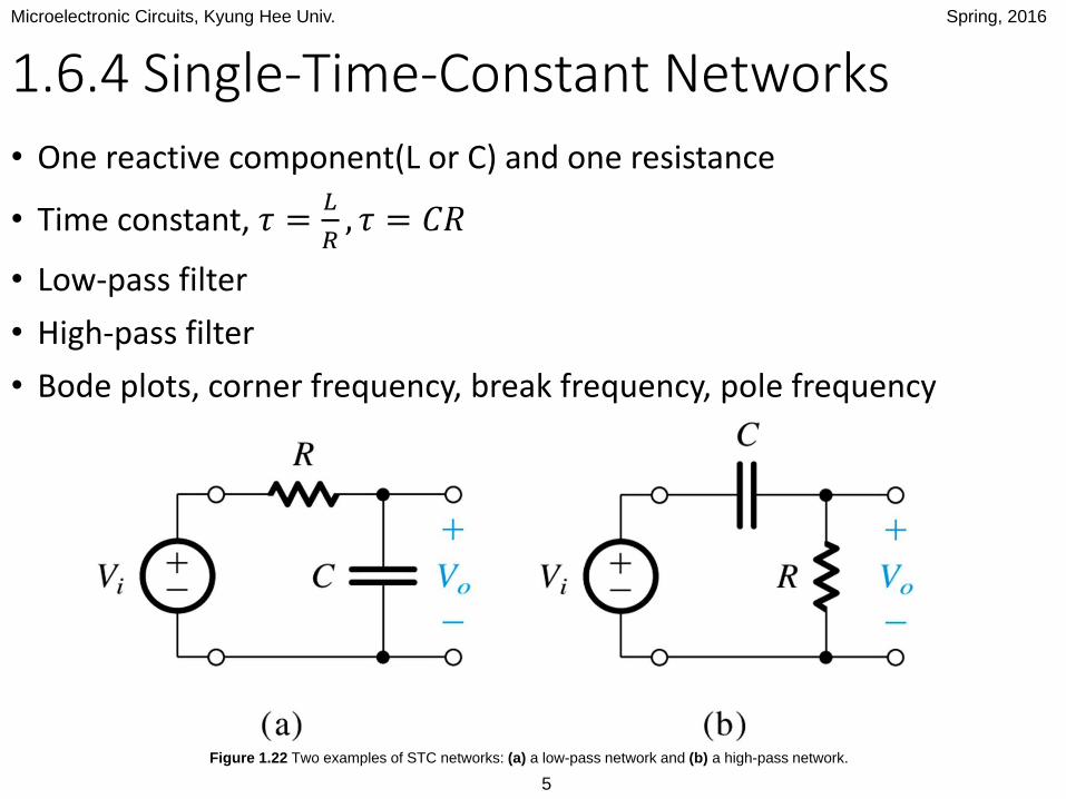
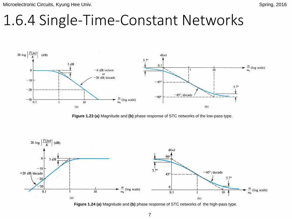
Figure 1.22 Two examples of STC networks: (a) a low-pass network and (b) a high-pass network.
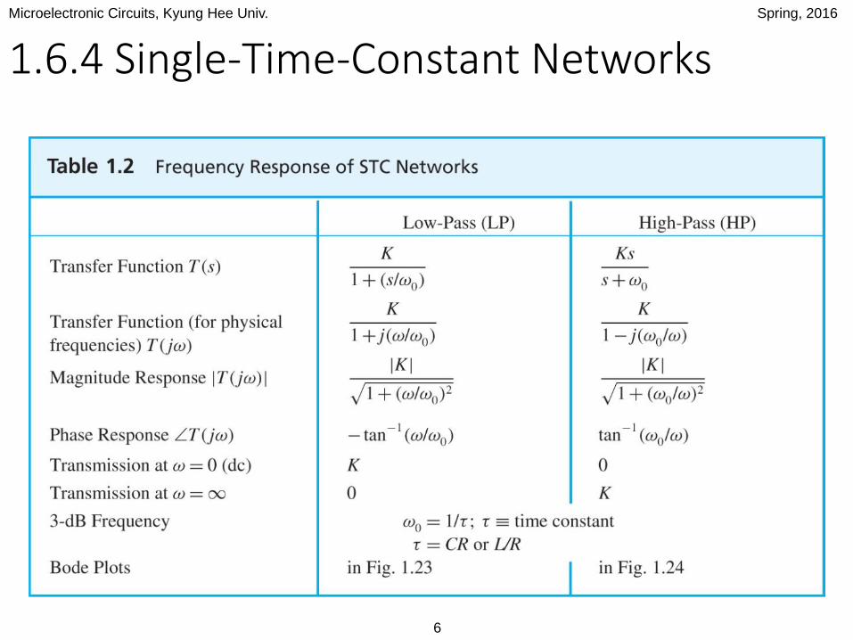
1.6.4 Single-Time-Constant Networks
• One reactive component(L or C) and one resistance
• Time constant, 𝜏 =𝐿
𝑅, 𝜏 = 𝐶𝑅
• Low-pass filter
• High-pass filter
• Bode plots, corner frequency, break frequency, pole frequency
Microelectronic Circuits, Kyung Hee Univ. Spring, 2016
6
1.6.4 Single-Time-Constant Networks
Microelectronic Circuits, Kyung Hee Univ. Spring, 2016
7
Figure 1.23 (a) Magnitude and (b) phase response of STC networks of the low-pass type.
Figure 1.24 (a) Magnitude and (b) phase response of STC networks of the high-pass type.
1.6.4 Single-Time-Constant Networks
Microelectronic Circuits, Kyung Hee Univ. Spring, 2016
8
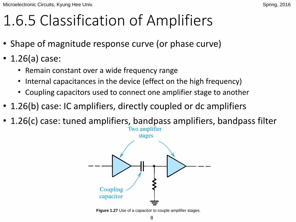
1.6.5 Classification of Amplifiers
• Shape of magnitude response curve (or phase curve)
• 1.26(a) case:• Remain constant over a wide frequency range
• Internal capacitances in the device (effect on the high frequency)
• Coupling capacitors used to connect one amplifier stage to another
• 1.26(b) case: IC amplifiers, directly coupled or dc amplifiers
• 1.26(c) case: tuned amplifiers, bandpass amplifiers, bandpass filter
Figure 1.27 Use of a capacitor to couple amplifier stages.
Microelectronic Circuits, Kyung Hee Univ. Spring, 2016
9
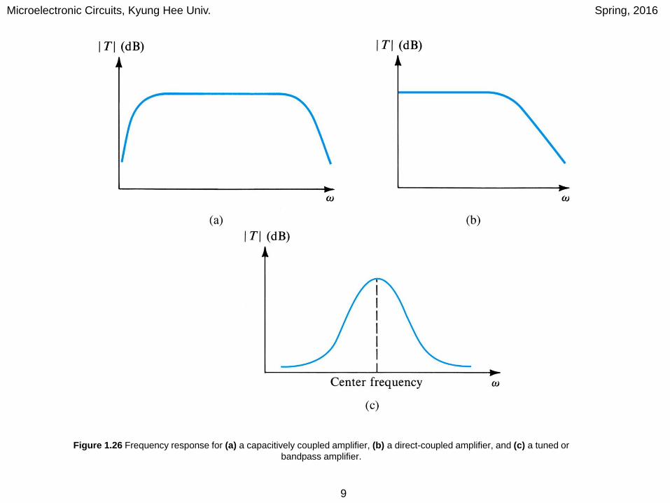
Figure 1.26 Frequency response for (a) a capacitively coupled amplifier, (b) a direct-coupled amplifier, and (c) a tuned or
bandpass amplifier.

Microelectronic Circuits, Kyung Hee Univ. Spring, 2016
10
Homeworks
• Example 1.5
Microelectronic Circuits, Kyung Hee Univ. Spring, 2016
11
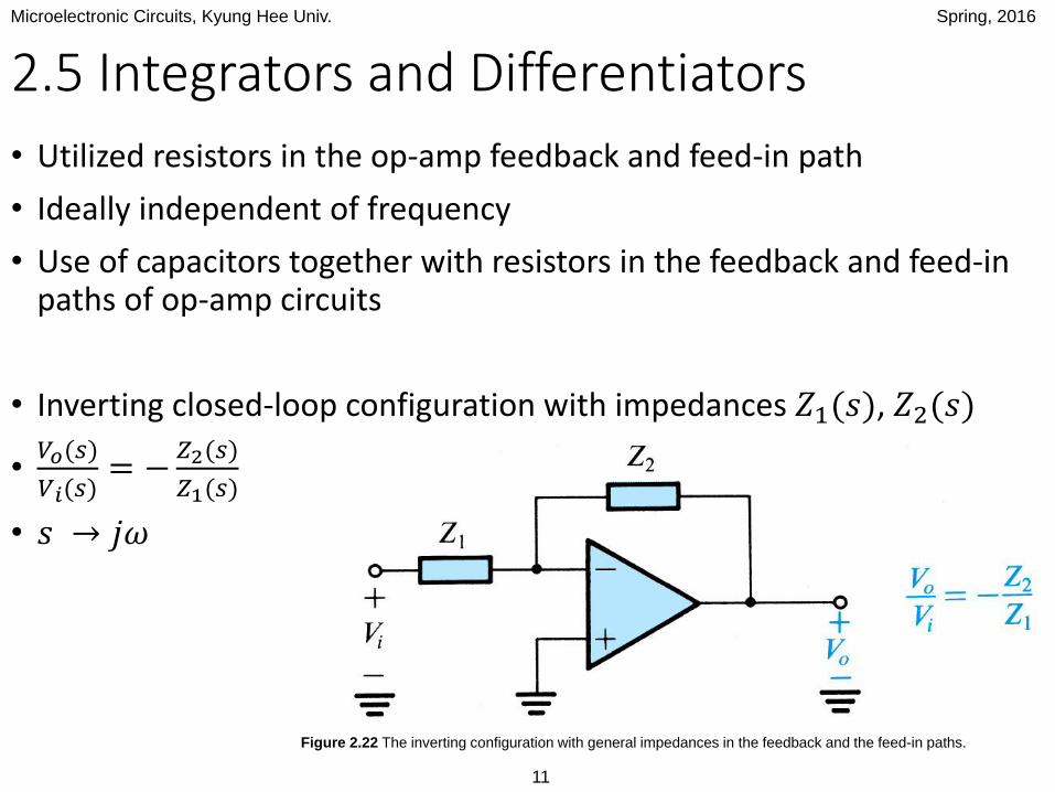
2.5 Integrators and Differentiators
• Utilized resistors in the op-amp feedback and feed-in path
• Ideally independent of frequency
• Use of capacitors together with resistors in the feedback and feed-in paths of op-amp circuits
• Inverting closed-loop configuration with impedances 𝑍1(𝑠), 𝑍2(𝑠)
•𝑉𝑜(𝑠)
𝑉𝑖(𝑠)= −
𝑍2(𝑠)
𝑍1(𝑠)
• 𝑠 → 𝑗𝜔
Figure 2.22 The inverting configuration with general impedances in the feedback and the feed-in paths.
Microelectronic Circuits, Kyung Hee Univ. Spring, 2016
12
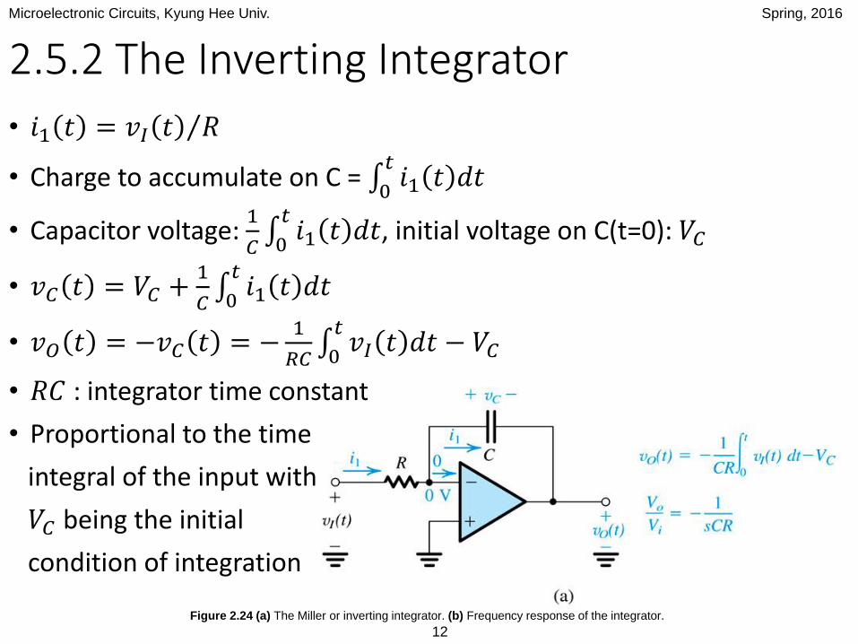
2.5.2 The Inverting Integrator
• 𝑖1 𝑡 = 𝑣𝐼 𝑡 𝑅
• Charge to accumulate on C = 0𝑡𝑖1 𝑡 𝑑𝑡
• Capacitor voltage: 1
𝐶 0𝑡𝑖1 𝑡 𝑑𝑡, initial voltage on C(t=0): 𝑉𝐶
• 𝑣𝐶 𝑡 = 𝑉𝐶 +1
𝐶 0𝑡𝑖1 𝑡 𝑑𝑡
• 𝑣𝑂 𝑡 = −𝑣𝐶 𝑡 = −1
𝑅𝐶 0𝑡𝑣𝐼 𝑡 𝑑𝑡 − 𝑉𝐶
• 𝑅𝐶 : integrator time constant
• Proportional to the time
integral of the input with
𝑉𝐶 being the initial
condition of integration
Figure 2.24 (a) The Miller or inverting integrator. (b) Frequency response of the integrator.
Microelectronic Circuits, Kyung Hee Univ. Spring, 2016
13
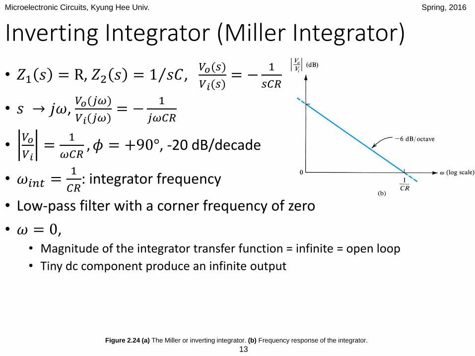
Inverting Integrator (Miller Integrator)
• 𝑍1 𝑠 = R, 𝑍2 𝑠 = 1 𝑠𝐶, 𝑉𝑜(𝑠)
𝑉𝑖(𝑠)= −
1
𝑠𝐶𝑅
• 𝑠 → 𝑗𝜔, 𝑉𝑜(𝑗𝜔)
𝑉𝑖(𝑗𝜔)= −
1
𝑗𝜔𝐶𝑅
•𝑉𝑜
𝑉𝑖=
1
𝜔𝐶𝑅, 𝜙 = +90°, -20 dB/decade
• 𝜔𝑖𝑛𝑡 =1
𝐶𝑅: integrator frequency
• Low-pass filter with a corner frequency of zero
• 𝜔 = 0, • Magnitude of the integrator transfer function = infinite = open loop
• Tiny dc component produce an infinite output
Figure 2.24 (a) The Miller or inverting integrator. (b) Frequency response of the integrator.
Microelectronic Circuits, Kyung Hee Univ. Spring, 2016
14
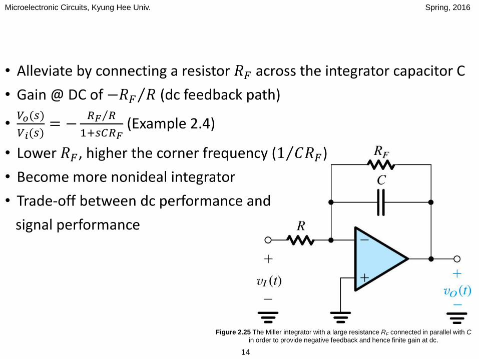
• Alleviate by connecting a resistor 𝑅𝐹 across the integrator capacitor C
• Gain @ DC of −𝑅𝐹 𝑅 (dc feedback path)
•𝑉𝑜(𝑠)
𝑉𝑖(𝑠)= −
𝑅𝐹 𝑅
1+𝑠𝐶𝑅𝐹(Example 2.4)
• Lower 𝑅𝐹, higher the corner frequency ( 1 𝐶𝑅𝐹)
• Become more nonideal integrator
• Trade-off between dc performance and
signal performance
Figure 2.25 The Miller integrator with a large resistance RF connected in parallel with C
in order to provide negative feedback and hence finite gain at dc.
Microelectronic Circuits, Kyung Hee Univ. Spring, 2016
15
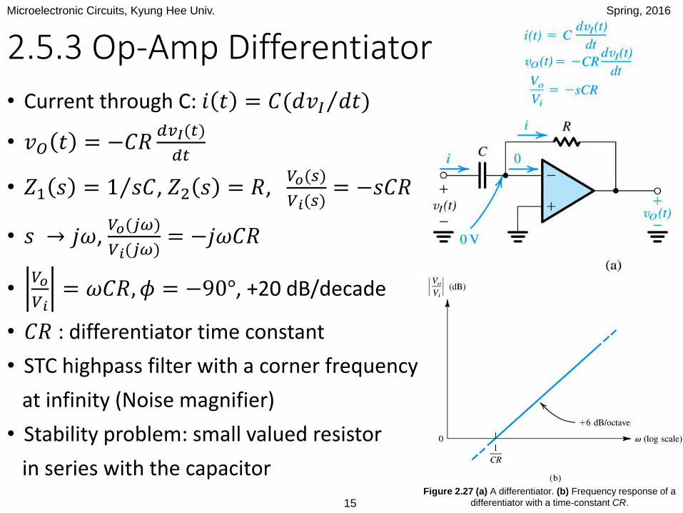
2.5.3 Op-Amp Differentiator
• Current through C: 𝑖 𝑡 = 𝐶(𝑑𝑣𝐼 𝑑𝑡)
• 𝑣𝑂 𝑡 = −𝐶𝑅𝑑𝑣𝐼(𝑡)
𝑑𝑡
• 𝑍1 𝑠 = 1 𝑠𝐶, 𝑍2 𝑠 = 𝑅, 𝑉𝑜(𝑠)
𝑉𝑖(𝑠)= −𝑠𝐶𝑅
• 𝑠 → 𝑗𝜔, 𝑉𝑜(𝑗𝜔)
𝑉𝑖(𝑗𝜔)= −𝑗𝜔𝐶𝑅
•𝑉𝑜
𝑉𝑖= 𝜔𝐶𝑅,𝜙 = −90°, +20 dB/decade
• 𝐶𝑅 : differentiator time constant
• STC highpass filter with a corner frequency
at infinity (Noise magnifier)
• Stability problem: small valued resistor
in series with the capacitorFigure 2.27 (a) A differentiator. (b) Frequency response of a
differentiator with a time-constant CR.
Microelectronic Circuits, Kyung Hee Univ. Spring, 2016
16
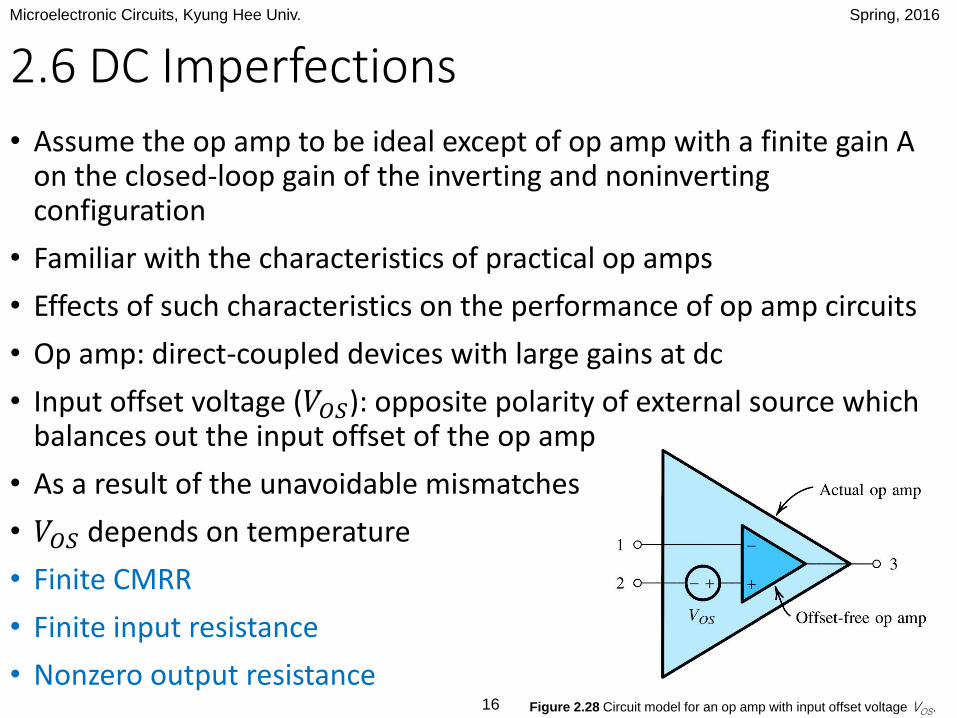
2.6 DC Imperfections
• Assume the op amp to be ideal except of op amp with a finite gain A on the closed-loop gain of the inverting and noninverting configuration
• Familiar with the characteristics of practical op amps
• Effects of such characteristics on the performance of op amp circuits
• Op amp: direct-coupled devices with large gains at dc
• Input offset voltage (𝑉𝑂𝑆): opposite polarity of external source which balances out the input offset of the op amp
• As a result of the unavoidable mismatches
• 𝑉𝑂𝑆 depends on temperature
• Finite CMRR
• Finite input resistance
• Nonzero output resistanceFigure 2.28 Circuit model for an op amp with input offset voltage VOS.
Microelectronic Circuits, Kyung Hee Univ. Spring, 2016
17
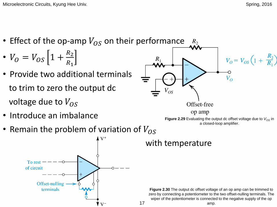
• Effect of the op-amp 𝑉𝑂𝑆 on their performance
• 𝑉𝑂 = 𝑉𝑂𝑆 1 +𝑅2
𝑅1
• Provide two additional terminals
to trim to zero the output dc
voltage due to 𝑉𝑂𝑆
• Introduce an imbalance
• Remain the problem of variation of 𝑉𝑂𝑆
with temperature
Figure 2.29 Evaluating the output dc offset voltage due to VOS in
a closed-loop amplifier.
Figure 2.30 The output dc offset voltage of an op amp can be trimmed to
zero by connecting a potentiometer to the two offset-nulling terminals. The
wiper of the potentiometer is connected to the negative supply of the op
amp.
Microelectronic Circuits, Kyung Hee Univ. Spring, 2016
18
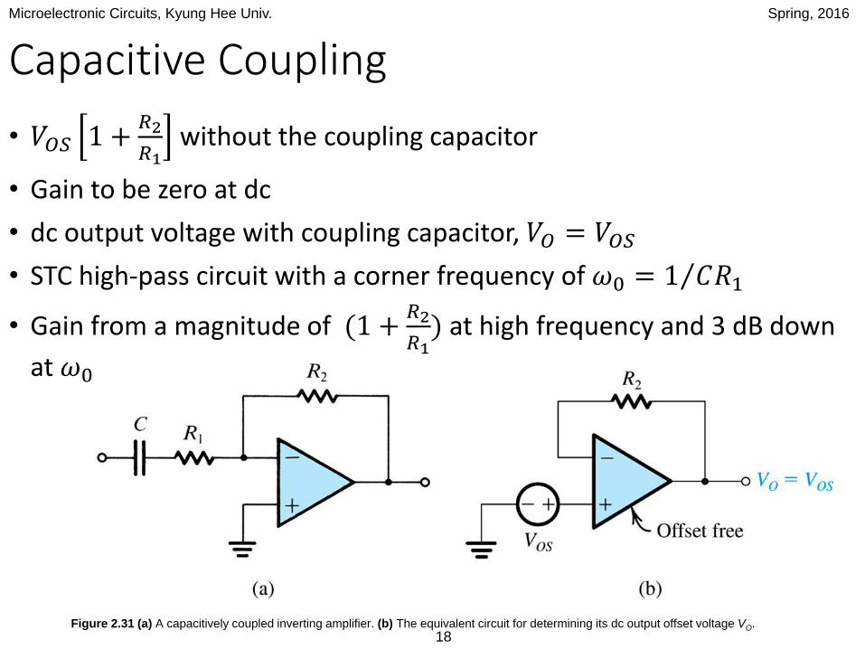
Capacitive Coupling
• 𝑉𝑂𝑆 1 +𝑅2
𝑅1without the coupling capacitor
• Gain to be zero at dc
• dc output voltage with coupling capacitor, 𝑉𝑂 = 𝑉𝑂𝑆
• STC high-pass circuit with a corner frequency of 𝜔0 = 1 𝐶𝑅1
• Gain from a magnitude of (1 +𝑅2
𝑅1) at high frequency and 3 dB down
at 𝜔0
Figure 2.31 (a) A capacitively coupled inverting amplifier. (b) The equivalent circuit for determining its dc output offset voltage VO.
Microelectronic Circuits, Kyung Hee Univ. Spring, 2016
19
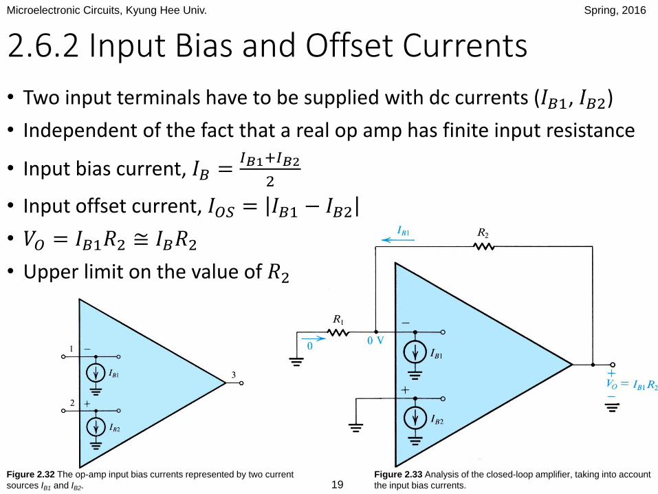
2.6.2 Input Bias and Offset Currents
• Two input terminals have to be supplied with dc currents (𝐼𝐵1, 𝐼𝐵2)
• Independent of the fact that a real op amp has finite input resistance
• Input bias current, 𝐼𝐵 =𝐼𝐵1+𝐼𝐵2
2
• Input offset current, 𝐼𝑂𝑆 = 𝐼𝐵1 − 𝐼𝐵2
• 𝑉𝑂 = 𝐼𝐵1𝑅2 ≅ 𝐼𝐵𝑅2
• Upper limit on the value of 𝑅2
Figure 2.32 The op-amp input bias currents represented by two current
sources IB1 and IB2.
Figure 2.33 Analysis of the closed-loop amplifier, taking into account
the input bias currents.
Microelectronic Circuits, Kyung Hee Univ. Spring, 2016
20
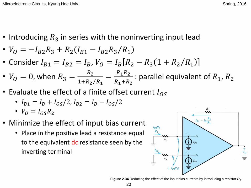
• Introducing 𝑅3 in series with the noninverting input lead
• 𝑉𝑂 = −𝐼𝐵2𝑅3 + 𝑅2 𝐼𝐵1 − 𝐼𝐵2𝑅3 𝑅1
• Consider 𝐼𝐵1 = 𝐼𝐵2 = 𝐼𝐵, 𝑉𝑂 = 𝐼𝐵 𝑅2 − 𝑅3 1 + 𝑅2 𝑅1
• 𝑉𝑂 = 0, when 𝑅3 =𝑅2
1+ 𝑅2 𝑅1=
𝑅1𝑅2
𝑅1+𝑅2: parallel equivalent of 𝑅1, 𝑅2
• Evaluate the effect of a finite offset current 𝐼𝑂𝑆• 𝐼𝐵1 = 𝐼𝐵 + 𝐼𝑂𝑆/2, 𝐼𝐵2 = 𝐼𝐵 − 𝐼𝑂𝑆/2
• 𝑉𝑂 = 𝐼𝑂𝑆𝑅2
• Minimize the effect of input bias current• Place in the positive lead a resistance equal
to the equivalent dc resistance seen by the
inverting terminal
Figure 2.34 Reducing the effect of the input bias currents by introducing a resistor R3.
Microelectronic Circuits, Kyung Hee Univ. Spring, 2016
21
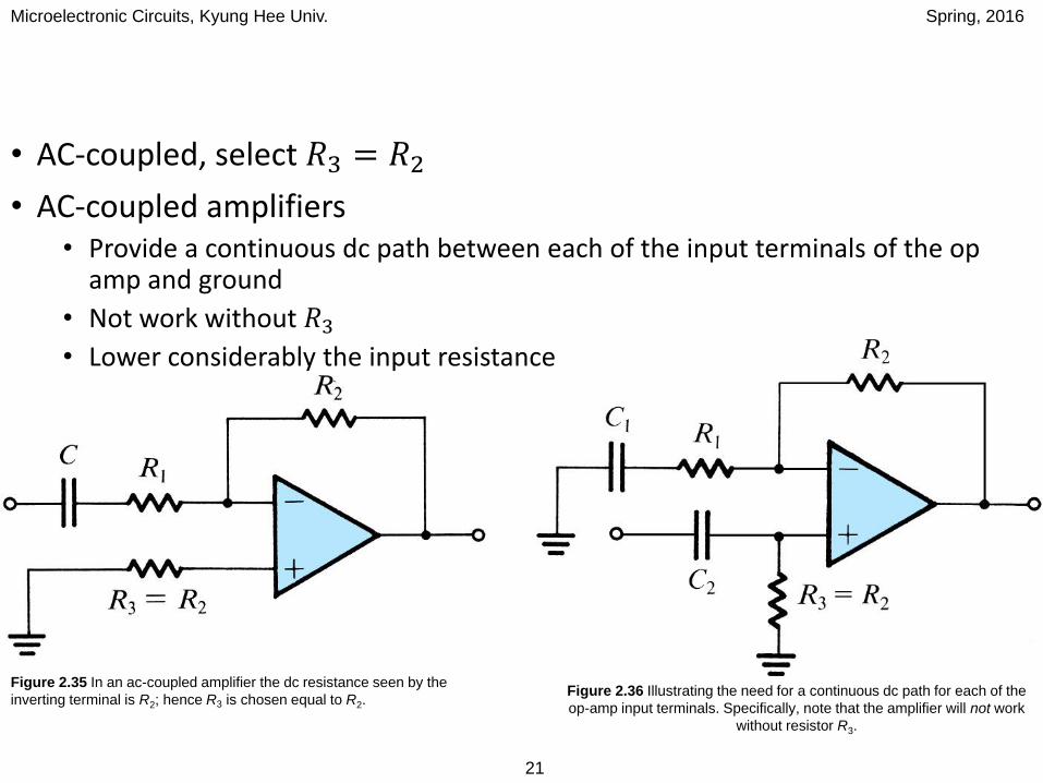
Figure 2.36 Illustrating the need for a continuous dc path for each of the
op-amp input terminals. Specifically, note that the amplifier will not work
without resistor R3.
• AC-coupled, select 𝑅3 = 𝑅2
• AC-coupled amplifiers• Provide a continuous dc path between each of the input terminals of the op
amp and ground
• Not work without 𝑅3• Lower considerably the input resistance
Figure 2.35 In an ac-coupled amplifier the dc resistance seen by the
inverting terminal is R2; hence R3 is chosen equal to R2.
Microelectronic Circuits, Kyung Hee Univ. Spring, 2016
22
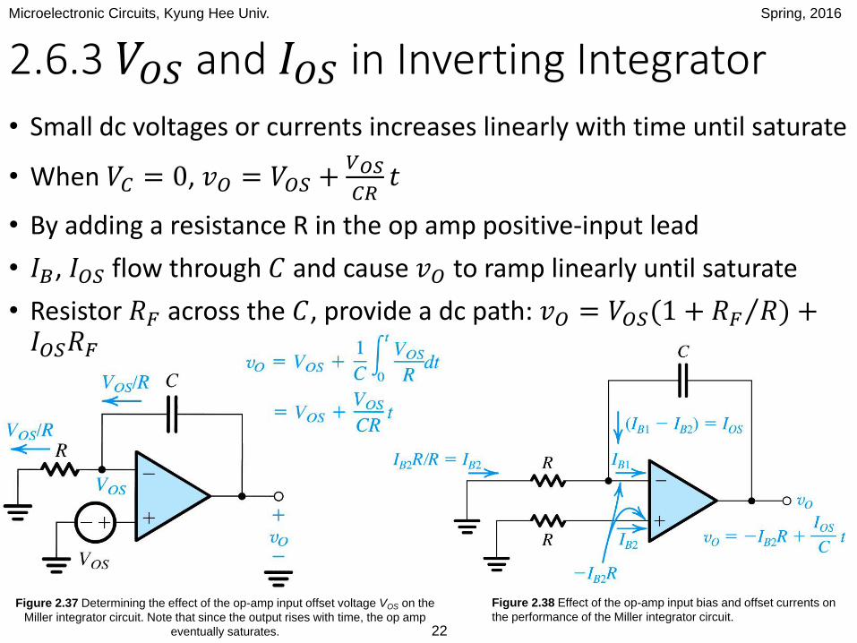
2.6.3 𝑉𝑂𝑆 and 𝐼𝑂𝑆 in Inverting Integrator
• Small dc voltages or currents increases linearly with time until saturate
• When 𝑉𝐶 = 0, 𝑣𝑂 = 𝑉𝑂𝑆 +𝑉𝑂𝑆
𝐶𝑅𝑡
• By adding a resistance R in the op amp positive-input lead
• 𝐼𝐵, 𝐼𝑂𝑆 flow through 𝐶 and cause 𝑣𝑂 to ramp linearly until saturate
• Resistor 𝑅𝐹 across the 𝐶, provide a dc path: 𝑣𝑂 = 𝑉𝑂𝑆(1 + 𝑅𝐹 𝑅) +𝐼𝑂𝑆𝑅𝐹
Figure 2.37 Determining the effect of the op-amp input offset voltage VOS on the
Miller integrator circuit. Note that since the output rises with time, the op amp
eventually saturates.
Figure 2.38 Effect of the op-amp input bias and offset currents on
the performance of the Miller integrator circuit.

Microelectronic Circuits, Kyung Hee Univ. Spring, 2016
23
Homeworks
• Example 2.4
• Example 2.5