Embed Size (px)
Citation preview

Microelectronics Research Center, The University of Texas at AustinMicroelectronics Research Center, The University of Texas at AustinMicrotechnologies for the New Millennium 2005Microtechnologies for the New Millennium 2005
Dean P. Neikirk and Sangwook Han Microelectronics Research Center
Department of Electrical and Computer EngineeringThe University of Texas at Austin
Austin, TX 78712USA
SPIE’s Microtechnologies for the New Millennium15-18 May 2003
Hotel Meliá SevillaSevilla, Spain
Proceedings of SPIE Vol. #5836 : Smart Sensors, Actuators, and MEMSSESSION 16, Room: Arenal I
Wed. May 18, 12.00 to 13.00: Infrared Sensors12.20-12.35: Design of infrared wavelength-selective microbolometers using planar multimode detectors, D. P. Neikirk, S. Han, Univ. of Texas/Austin (USA) [5836-60]
link to pdf of proceedings paper .
Design of Infrared Wavelength-Selective Design of Infrared Wavelength-Selective Microbolometers Using Planar Multimode Microbolometers Using Planar Multimode
DetectorsDetectors

Microelectronics Research Center, The University of Texas at AustinMicroelectronics Research Center, The University of Texas at AustinMicrotechnologies for the New Millennium 2005Microtechnologies for the New Millennium 2005 2
Fabry-Perot Microbolometer Array
dmirror
resistive sheet
http://lep694.gsfc.nasa.gov/code693/tdw03/proceedings/docs/session_2/Ngo.pdf
Conventional microbolometer infrared
focal plane detectors• in an ideal device, the absorber should p
rovide total absorption of the incoming radiation and convert the electromagnetic radiation into heat
• to “match” an absorber to free space requires
– absorber: e.g., a thin conductor with sheet resistance 377 ohms
– mirror placed (odd integer)·/4 behind absorbing layer
– essentially a Fabry-Perot cavity– this is sometimes referred to as “space cl
oth”
incident
thin conductor(absorber)
Mirror layer
Gap
4
odd

Microelectronics Research Center, The University of Texas at AustinMicroelectronics Research Center, The University of Texas at AustinMicrotechnologies for the New Millennium 2005Microtechnologies for the New Millennium 2005 3
Spectral response of Fabry-Perot microbolometers
377
mirror
• is it possible to build “multi-color” IR F-P microbolometer focal plane arrays?– the primary “design variable” is the distance to the mirror
3 m gap
2.5 m gap
2 m gap
LWIR
wavelength (microns)
cou
pli
ng
eff
icie
ncy
4 6 8 10 12 14
0.2
0.4
0.6
0.8
0
1
the bandwidth of conventional Fabry-Perot microbolometers is too wide to allow easy “color” discrimination in the LWIR wavelength band

Microelectronics Research Center, The University of Texas at AustinMicroelectronics Research Center, The University of Texas at AustinMicrotechnologies for the New Millennium 2005Microtechnologies for the New Millennium 2005 4
Single Element in Array
g
w
a
d
metal grid
mirror
resistive microbolometer
Planar Multimode Detector Array
metal grid
mirror
Alternative: planar multimode detectors
• replace standard thin film bolometer with a true antenna coupled microbolometer array– essentially a
resistively loaded inductive/capacitive mesh
– planar multimode detectors were extensively studied for infrared and millimeter wave detection by Rutledge and Schwarz in the late 1970’s

Microelectronics Research Center, The University of Texas at AustinMicroelectronics Research Center, The University of Texas at AustinMicrotechnologies for the New Millennium 2005Microtechnologies for the New Millennium 2005 5
Planar Multimode Detectors
support layerresistive microbolometer
gridmirror
single pixelsingle pixel
η0 η0jBcjBl
Gd
Zin d
grid equivalent mirror equivalentarrayarray
• grid period a < the shortest wavelength• analysis can be performed using a
modification of Eisenhart & Kahn’s waveguide post model
single periodsingle period
a g
d
w

Microelectronics Research Center, The University of Texas at AustinMicroelectronics Research Center, The University of Texas at AustinMicrotechnologies for the New Millennium 2005Microtechnologies for the New Millennium 2005 6
Spectral response of planar multimode grids
Blue
a NA
g NA
w NA
d 2.50
Rs 377Ω
all lengths in [micron]
• grid response depends on array period a, gap g, post width w, distance to mirror d, and sheet resistance RS of microbolometer material
space cloth
7 8 9 10 11 12 13 14wavelength [micron]
0
0.5
1
po
we
r ab
sorp
tio
n e
ffic
ien
cy
*
*
377Ω
2.50
4.50
5.00
7.00
Mag
30Ω
3.61
0.96
1.00
5.33
Green
53.5Ω
3.29
3.00
0.20
6.90
Red
• wide range of achievable bandwidths, from broad to narrow
grida g
dw
Microelectronics Research Center, The University of Texas at AustinMicroelectronics Research Center, The University of Texas at AustinMicrotechnologies for the New Millennium 2005Microtechnologies for the New Millennium 2005 7
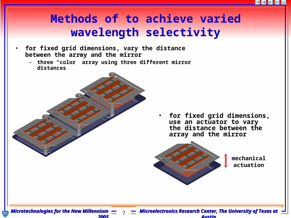
Methods of to achieve varied wavelength selectivity
mechanical actuation
• for fixed grid dimensions, vary the distance between the array and the mirror
– three “color” array using three different mirror distances
• for fixed grid dimensions, use an actuator to vary the distance between the array and the mirror

Microelectronics Research Center, The University of Texas at AustinMicroelectronics Research Center, The University of Texas at AustinMicrotechnologies for the New Millennium 2005Microtechnologies for the New Millennium 2005 8
d=0μm
d=6μm
d
10 20 30 40 50 60 70 80 90 100
20
40
60
80
100
120
140
160
180
200
0.1
0.2
0.3
0.4
0.5
0.6
0.7
0.8
0.9
0 62 41 3 5d in [μm]
7
14
13
12
11
10
9
8
wav
elen
gth
in [
μm]
power absorption efficiency
7 8 9 10 11 12 13 140
0.1
0.2
0.3
0.4
0.5
0.6
0.7
0.8
0.9
1
wavelength in [micron]
po
we
r a
bs
orp
tio
n e
ffic
ien
cy
d=3.29μm
a=6.90μm
g=0.20μm
w=3.00μm
Rs=53.5Ω
Wavelength selectivity varied by changing distance d to the mirror
• narrow spectral response allows greater “color” sensitivity

Microelectronics Research Center, The University of Texas at AustinMicroelectronics Research Center, The University of Texas at AustinMicrotechnologies for the New Millennium 2005Microtechnologies for the New Millennium 2005 9
Selecting spectral response for “color” pixels
7 8 9 10 11 12 13 140
1
0
1
0
1
wavelength in [micron]
pow
er a
bsor
ptio
n ef
fici
ency
7 8 9 10 11 12 13 140
1
0
1
0
1
wavelength in [micron]
pow
er a
bsor
ptio
n ef
fici
ency
ideal ambiguous
• if a design produces more than one peak in absorption then the “color” becomes ambiguous
pixel 1
pixel 2
pixel 3
“ghost” peak

Microelectronics Research Center, The University of Texas at AustinMicroelectronics Research Center, The University of Texas at AustinMicrotechnologies for the New Millennium 2005Microtechnologies for the New Millennium 2005 10
Achieving wavelength selectivity by varying d
d=3.29 micron
d=5.70 micron
d
10 20 30 40 50 60 70 80 90 100
20
40
60
80
100
120
140
160
180
200
0.1
0.2
0.3
0.4
0.5
0.6
0.7
0.8
0.9
0 62 41 3 5d in [micron]
7
14
13
12
11
10
9
8wav
elen
gth
in [
mic
ron]
power absorption efficiency
7 8 9 10 11 12 13 140
0.1
0.2
0.3
0.4
0.5
0.6
0.7
0.8
0.9
1
wavelength in [micron]
po
we
r a
bs
orp
tio
n e
ffic
ien
cy
a=6.90 microng=0.20 micronw=3.00 micronRs=53.5Ω
““ghost” peak: ghost” peak: badbad
7 8 9 10 11 12 13 14wavelength in [micron]
7 8 9 10 11 12 13 140
0.1
0.2
0.3
0.4
0.5
0.6
0.7
0.8
0.9
1
wavelength in [micron]
po
we
r a
bs
orp
tio
n e
ffic
ien
cy
0
1
power absorption efficiency
GoodGood
GoodGood

Microelectronics Research Center, The University of Texas at AustinMicroelectronics Research Center, The University of Texas at AustinMicrotechnologies for the New Millennium 2005Microtechnologies for the New Millennium 2005 11
7 8 9 10 11 12 13 140
0.1
0.2
0.3
0.4
0.5
0.6
0.7
0.8
0.9
1
wavelength in [micron]
po
we
r a
bs
orp
tio
n e
ffic
ien
cy
d=2.0micron
d=2.5micrond=3.0micronRs=377Ω
7 8 9 10 11 12 13 14wavelength in [micron]
1
pow
er a
bsor
ptio
n ef
fici
ency
07 8 9 10 11 12 13 14
0
0.1
0.2
0.3
0.4
0.5
0.6
0.7
0.8
0.9
1
wavelength in [micron]
po
we
r a
bs
orp
tio
n e
ffic
ien
cy
d=1.65micrond=3.75micron
d=5.10micron
a=5.07microng=1.43micronw=0.74micron
Rs=21.0Ω
7 8 9 10 11 12 13 14wavelength in [micron]
1
pow
er a
bsor
ptio
n ef
fici
ency
0
Space clothSpace cloth
Optimized 3-color wavelength selectivity by varying only d
optimization performed using a genetic algorithm
– design goal: three minimum width spectral peaks centered at 8, 10 and 12 microns
insufficient spectral insufficient spectral selectivityselectivity

Microelectronics Research Center, The University of Texas at AustinMicroelectronics Research Center, The University of Texas at AustinMicrotechnologies for the New Millennium 2005Microtechnologies for the New Millennium 2005 12
7 8 9 10 11 12 13 140
0.1
0.2
0.3
0.4
0.5
0.6
0.7
0.8
0.9
1
wavelength in [micron]
pow
er
abs
orp
tion
effi
cie
ncy
Problem with variable d: complex fabrication
processes
• requires either– fabrication process with three different
sacrificial layer thicknesses
• or– mems actuator
• in both cases the fabrication would be more complicated than current micromachined microbolometer focal plane array processes
– there is still some color ambiguity for the longest wavelength (12 micron) pixel
• due to “ghost” peak at 7 microns

Microelectronics Research Center, The University of Texas at AustinMicroelectronics Research Center, The University of Texas at AustinMicrotechnologies for the New Millennium 2005Microtechnologies for the New Millennium 2005 13
Wavelength selectivity by varying lithographically-drawn parameters
a g
d
w• potentially simpler process if the sacrificial layer is held
fixed for all pixels– sheet resistance of bolometer material also held
constant (same material for all pixels)– vary ONLY the lithographically drawn features of the
grid• array period a, gap width g, and post width w

Microelectronics Research Center, The University of Texas at AustinMicroelectronics Research Center, The University of Texas at AustinMicrotechnologies for the New Millennium 2005Microtechnologies for the New Millennium 2005 14
Optimized designs• genetic algorithm used for optimization
– design goal: three minimum width spectral peaks centered at 8, 10 and 12 microns– constraints:
• d (distance to mirror) is varied, but must be the same under all three pixels• sheet resistance of bolometer material also held constant• vary only grid period a, gap width g, and post width w
w = 4.57m
wavelength in [micron]8 9 10 11 12 13 140
0.1
0.2
0.3
0.4
0.5
0.6
0.7
0.8
0.9
1
7
pow
er a
bsor
ptio
n e
ffic
ienc
y
w = 2.80m
w = 1.30m
• results from design optimization
– optimum distance to mirror d = 3.14 m
– optimum RS = 56.6 – all three pixels share co
mmon grid period a and gap width g
• a = 6.80 m• g = 0.20 m
– post width w is critical in determining location of absorption peak

Microelectronics Research Center, The University of Texas at AustinMicroelectronics Research Center, The University of Texas at AustinMicrotechnologies for the New Millennium 2005Microtechnologies for the New Millennium 2005 15
abso
rpti
on
Comparison: power absorption efficienciespower absorption efficiencies
7 8 9 10 11 12 13 140
0.1
0.2
0.3
0.4
0.5
0.6
0.7
0.8
0.9
1
wavelength in [micron]
po
we
r a
bs
orp
tio
n e
ffic
ien
cy
7 8 9 10 11 12 13 140
0.1
0.2
0.3
0.4
0.5
0.6
0.7
0.8
0.9
1
wavelength in [micron]
po
we
r a
bs
orp
tio
n e
ffic
ien
cy
7 8 9 10 11 12 13 140
0.1
0.2
0.3
0.4
0.5
0.6
0.7
0.8
0.9
1
wavelength in [micron]
po
we
r a
bs
orp
tio
n e
ffic
ien
cy
7 14wavelength in [micron]
0
1
7 14 7 14
Fabry-Perot microbolometer
variable mirror grid microbolometer
grid dimensions varied

Microelectronics Research Center, The University of Texas at AustinMicroelectronics Research Center, The University of Texas at AustinMicrotechnologies for the New Millennium 2005Microtechnologies for the New Millennium 2005 16
IR wavelength-selective focal plane arrays
• planar multimode detectors exhibit widely tunable spectral response– can tune for much narrower spectral response than conventional
Fabry-Perot microbolometers
• tuning of wavelength response can be achieved using several methods– for fixed grid dimensions distance to tuning mirror can be used
• multiple sacrificial layer thicknesses
• mechanical actuation
• a wavelength-selective three pixel design, each pixel using different lithographically drawn dimensions with constant mirror separation, shows excellent narrow band response
• through the use of planar multimode detectors color vision in the long wavelength band should be achievable