Embed Size (px)
Citation preview

ACTAUNIVERSITATIS
UPSALIENSISUPPSALA
2017
Digital Comprehensive Summaries of Uppsala Dissertationsfrom the Faculty of Science and Technology 1513
Microfabricated Gas Sensors Basedon Hydrothermally Grown 1-DZnO Nanostructures
MINGZHI JIAO
ISSN 1651-6214ISBN 978-91-554-9908-2urn:nbn:se:uu:diva-320183
Dissertation presented at Uppsala University to be publicly examined in 2001,Ångströmlaboratoriet, Lägerhyddsvägen 1, Uppsala, Friday, 9 June 2017 at 09:15 for thedegree of Doctor of Philosophy. The examination will be conducted in English. Facultyexaminer: Prof. Anita Lloyd Spetz.
AbstractJiao, M. 2017. Microfabricated Gas Sensors Based on Hydrothermally Grown 1-D ZnONanostructures. Digital Comprehensive Summaries of Uppsala Dissertations from theFaculty of Science and Technology 1513. 60 pp. Uppsala: Acta Universitatis Upsaliensis.ISBN 978-91-554-9908-2.
In this thesis, gas sensors based on on-chip hydrothermally grown 1-D zinc oxide (ZnO)nanostructures are presented, to improve the sensitivity, selectivity, and stability of the gassensors.
Metal-oxide-semiconductor (MOS) gas sensors are well-established tools for the monitoringof air quality indoors and outdoors. In recent years, the use of 1-D metal oxide nanostructures forsensing toxic gases, such as nitrogen dioxide, ammonia, and hydrogen, has gained significantattention. However, low-dimensional nanorod (NR) gas sensors can be enhanced further. Mostworks synthesize the NRs first and then transfer them onto electrodes to produce gas sensors,thereby resulting in large batch-to-batch difference.
Therefore, in this thesis six studies on 1-D ZnO NR gas sensors were carried out. First,ultrathin secondary ZnO nanowires (NWs) were successfully grown on a silicon substrate.Second, an on-chip hydrothermally grown ZnO NR gas sensor was developed on a glasssubstrate. Its performance with regard to sensing nitrogen dioxide and three reductive gases,namely, ethanol, hydrogen, and ammonia, was tested. Third, three 1-D ZnO nanostructures,namely, ZnO NRs, dense ZnO NWs, and sparse ZnO NWs, were synthesized and tested towardnitrogen dioxide. Fourth, hydrothermally grown ZnO NRs, chemical vapor deposited ZnO NWs,and thermal deposited ZnO nanoparticles (NPs) were tested toward ethanol. Fifth, the effect ofannealing on the sensitivity and stability of ZnO NR gas sensors was examined. Sixth, ZnO NRswere decorated with palladium oxide NPs and tested toward hydrogen at high temperature.
The following conclusions can be drawn from the work in this thesis: 1) ZnO NWs can beobtained by using a precursor at low concentration, temperature of 90 °C, and long reactiontime. 2) ZnO NR gas sensors have better selectivity to nitrogen dioxide compared with ethanol,ammonia, and hydrogen. 3) Sparse ZnO NWs are highly sensitive to nitrogen dioxide comparedwith dense ZnO NWs and ZnO NRs. 4) ZnO NPs have the highest sensitivity to ethanolcompared with dense ZnO NWs and ZnO NRs. The sensitivity of the NPs is due to their smallgrain sizes and large surface areas. 5) ZnO NRs annealed at 600 °C have lower sensitivity towardnitrogen dioxide but higher long-term stability compared with those annealed at 400 °C. 6)When decorated with palladium oxide, both materials form alloy at a temperature higher than350 °C and decrease the amount of ZnO, which is the sensing material toward hydrogen. Thus,controlling the amount of palladium oxide on ZnO NRs is necessary.
Keywords: gas sensor, zinc oxide, on-chip, hydrothermal growth, nanorods, nanowires,annealing, palladium oxide, photoluminescence, alloy, sensitivity, selectivity, stability
Mingzhi Jiao, Department of Engineering Sciences, Microsystems Technology, 516, UppsalaUniversity, SE-751 20 Uppsala, Sweden.
© Mingzhi Jiao 2017
ISSN 1651-6214ISBN 978-91-554-9908-2urn:nbn:se:uu:diva-320183 (http://urn.kb.se/resolve?urn=urn:nbn:se:uu:diva-320183)

To my family and all my friends


List of Papers
This thesis is based on the following papers, which are referred to in the text by their Roman numerals.
I Jiao, M., Nguyen, D.H., Nguyen, V.D., Nguyen, V.H., Hjort,
K., Nguyen, H. (2016) Controlled Synthesis and Understanding of Growth Mechanism – Parameters for Atmospheric Pressure Hydrothermal Synthesis of Ultrathin Secondary ZnO Nan-owires, J. Sci. Res. Reports. 9:1–10.
II Jiao, M., Nguyen, V.C., Nguyen, V.D., Nguyen, D.H., Nguyen, V.H., Hjort, K., Nguyen, H. (2016) On-chip hydrothermal growth of ZnO nanorods at low temperature for highly selective NO2 gas sensor, Mater. Lett. 169:231–235.
III Jiao, M., Nguyen, V.D., Nguyen, V.C., Nguyen, D.H., Nguyen,
V.H., Hjort, K., Nguyen, H. Comparison of NO2 gas sensing properties of three different ZnO nanostructures synthesized by on-chip low-temperature hydrothermal growth, submitted
IV Chu, T.Q., Chu, M.H., Nguyen V.D., Nguyen D.H., Jiao, M.,
Nguyen H. (2017) Ethanol-Sensing Characteristics of Nanostructured ZnO: Nanorods, Nanowires, and Porous Nano-particles Journal of Electronic Materials, DOI: 10.1007/s11664-016-5270-2
V Jiao, M., Nguyen, V.C., Nguyen, V.D., Nguyen, D.H., Nguyen,
V.H., Hjort, K., Nguyen, H. On-chip growth of patterned ZnO nanorod sensors with PdO decoration for enhancement of hy-drogen-sensing performance, under review
VI Jiao, M., Nguyen, V.C., Nguyen, V.D., Nguyen, D.H., Nguyen,
V.H., Hjort, K., Nguyen, H. Influence of annealing temperature on the performance of on-chip hydrothermally grown ZnO na-norod gas sensor toward NO2, submitted
Reprints were made with permission from the respective publishers.


Author´s contribution
Paper I Part of planning, major part of experimental and analysis, part of writing. Paper II Part of planning; major part of experimental, analysis, and writing. Paper III Part of planning; major part of experimental, analysis, and writing. Paper IV Part of experimental. Paper V Minor part of planning, part of experimental, all analysis, and major part of writing. Paper VI Major part of planning, experimental, analysis, and writing.


Contents
1. Introduction ............................................................................................... 13 1.1 Markets and types of gas sensors ....................................................... 13 1.2 MOS Gas sensors ............................................................................... 16 1.3. Sensing mechanisms of 1-D ZnO ...................................................... 21 1.4 Motivation .......................................................................................... 26
2. Experimental ............................................................................................. 28 2.1 Fabrication of gas sensor devices ....................................................... 28
2.1.1 Microfabrication ......................................................................... 28 2.1.2 Growth of 1-D ZnO nanostructures ............................................ 32
2.2. Characterization of ZnO Nanostructures ........................................... 32 2.2.1 Optical Microscopy .................................................................... 32 2.2.2 SEM with EDS ........................................................................... 33 2.2.2 TEM ............................................................................................ 34 2.2.3 XRD ............................................................................................ 34 2.2.4 Photoluminescence ..................................................................... 35 2.2.5 XPS ............................................................................................. 36
2.3 Gas sensing characterization .............................................................. 36
3. Summary of results ................................................................................... 39 3.1 Summary of Paper I ............................................................................ 39 3.2 Summary of Paper II .......................................................................... 40 3.3 Summary of Paper III ......................................................................... 41 3.4 Summary of Paper IV ......................................................................... 42 3.5 Summary of Paper V .......................................................................... 44 3.6 Summary of Paper VI ......................................................................... 46
Conclusion and outlook ................................................................................ 50
Sammanfatting På Svenska ........................................................................... 52
Acknowledgements ....................................................................................... 55
References ..................................................................................................... 57


Abbreviations
1-D One dimensional NR Nanorod NW Nanowire NP nanoparticle MOS Metal oxide semiconductor CVD Chemical vapor deposition PVD Physical vapor deposition PL Photoluminescence SEM Scanning Electron Microscopy TEM Transmission Electron Microscopy XRD X-ray diffraction XPS X-ray photoelectron spectroscopy EDS Energy-dispersive X-ray spectroscopy HMTA Hexamethylenetetramine LD Debye length Vsurface Surface potential kB Boltzmann constant, 1.38×10⁻²³ J/K ϵ0 the dielectric constant of vacuum, 8.85×10⁻¹² F/m

13
1. Introduction
1.1 Markets and types of gas sensors Gas sensors were invented because of the strong necessity to measure gas components in living environments. As early as 1941, a humidity control apparatus was patented to measure and control humidity in a closed space [1]. Apart from water vapor, many other gases are present in air. Some of these gases can be harmful to humans. Nitrogen dioxide and hydrogen sul-fide have strong odors and thus can be detected by human nose. By contrast, hydrogen and carbon dioxide are odorless and thus cannot be detected. Therefore, gas sensors must be used to detect and determine the concentra-tion of carbon dioxide and nitrogen dioxide in the air. Today, gas sensors can be found indoors and outdoors. Gas sensors have been applied in environ-mental monitoring, industrial control, home security, and even in agriculture. Nowadays, the Internet of Things can facilitate our life, and gas sensors are one of the key components in the area. The typical applications of gas sen-sors and their typical measured gases can be divided, as follows [2]: - Food and agriculture (humidity, CO2) - Automotive (O2, CO, NOX, SOX) - Health and breath analysis (NH3, C2H5OH) - Environment (CO, CO2, NOX, H2S) - Industry (O2, H2, CO, H2S) The market for gas sensors in Europe is growing, as shown in Figure 1 [3]. The gas sensor market is estimated to increase to approximately 750 million USD in 2020. Owing to the huge market for gas sensors and specific demand for gas sensors in different fields, research on gas sensors continues to pro-gress despite their long history.

14
Figure 1. Gas sensors in the European market (million USD) in 2012–2020 [3].
Gas sensors can be categorized according to target gases, as shown in the figure above. They can also be categorized according to types, on which their working principles are based, as shown in Table 1 [4].
Table 1. Types and mechanisms of common gas sensors. Courtesy of Alphus D. Wilson.
Sensor type Sensitive material Detection principleAcoustic: Quartz crystal microbalance, surface and bulk acoustic wave
Organic or inorganic film
Mass change (frequency shift)
Calorimetric: catalytic bead Pellistor Temperature or heat change Catalytic field-effect transis-tor
Catalytic metals Electrical field change
Colorimetric sensors Organic dyes Color changes, absorbance Conducting polymer sensors Modified conducting
polymerResistance
Electrochemical sensors Solid or liquid electro-lytes
Current or voltage change
Fluorescence sensors Fluorescence-sensitive detector
Fluorescent-light emission
Infrared sensors IR-sensitive detector Infrared-radiation adsorption Metal oxide semiconductor sensors
Semiconductor metal oxide
Resistance change
Optical sensors Photodiode Light modulation, optical changes
Gas sensors are evaluated mainly according to a number of parameters, which are listed and explained below [5].
• Response is the ratio between measured resistance in target gas and a reference resistance or the other way round. The reference resistance normally is the sensor resistance measured in dry air. Response is usually larger than 1.

15
• Sensitivity is the ratio between resistance change per target gas concentration unit, in other words, the slope of a measurement graph. Some researchers also use the physical definition of sensi-tivity, that is, the ratio between a resistance change and the refer-ence resistance.
• Selectivity reflects how well a sensor can respond to a single tar-get gas in a mixture containing another gas, that is, selectivity is the ratio between the responses of two gases.
• Stability is the ability of a sensor to provide the same results. Therefore, the sensitivity, selectivity, response, and recovery time of the sensor remains unchanged.
• Response time (tR) is the time a sensor needs to respond to a target gas after the gas concentration changes from zero to a certain val-ue.
• Recovery time is the time required for the sensor signal to return to its starting point after the target gas concentration has dropped to zero.
• Size and cost • Power consumption • Operation temperature (TOPE)
A gas sensor is selected on the basis of specific application requirements, such as working temperature range, sensitivity, and selectivity. The selection of a sensor should also be based on the advantages and disadvantages of a specific sensor. For example, electrochemical gas sensors can work at ambient temperature and require low power. However, their sensitivity to low-weight gas is low. Optical gas sensors have high sensitivity and selectivity. However, they are expensive and often not portable. The advantages and disadvantages of the most commonly used gas sensors are shown in Table 2 [4]:
Table 2. Pros and cons of some most commonly used gas sensor types. Courtesy of Alphus D. Wilson.
Sensor type Pros ConsCalorimetric High selectivity for oxidative
compounds, short tRHigh TOPE, only sensitive to oxidative compounds
Catalytic field-effect transistor
Stability, wide TOPE range, small size
Requires environmental control, baseline drift
Electrochemical Ambient TOPE, low power, sensi-tive to diverse VOCs
Bulky size, limited sensitivi-ty to low weight gas
Metal oxide semi-conductor
High sensitivity, limited sensing range, short tR for low weight gas
High TOPE, high power, sensitive to humidity
Optical High sensitivity and selectivity Expensive, low portability, complex sensor array system

16
1.2 MOS Gas sensors Among all types of gas sensors, the MOS gas sensor, also called metal oxide chemoresistive gas sensor, may be the most interesting type because of its low cost, high stability, and easy integration with electronics. Research on MOS gas sensors has been conducted for more than 50 years [6]. In 1962, Seiyama demonstrated that a ZnO thin film can quickly change its resistance at 485 °C [7]. A simple chemoresistive device had 100 times higher response to propane compared with that of thermal conductivity detector in gas chromatography at that time. Shaver activated the SnO2 surface with an ultrathin Pt layer and found that the sensor responded quickly to hydrogen [8]. When activated with Pt, metal oxides, such as MoO3, Cr2O3, TiO2, and NiO, exhibit rapid resistance changes to airborne hydrogen at 300 °C as well. Since then, the sensitivity and selectivity of MOS gas sensor have been improved significantly by doping the metal oxides with other catalytic metals, and many new metal oxides have also been tested as gas-sensing materials.
All of the metal oxides used in MOS gas sensors can be divided into n-type or p-type depending on their charge carrier type. Typical n-type metal oxides are SnO2, ZnO, TiO2, WO3, In2O3, and Fe2O3, while typical p-type metal oxides are CuO, NiO, Co3O4, and Cr2O3. ZnO is usually sensitive to NO2 and C2H5OH, whereas CuO is often sensitive to H2S. Metal oxide surfaces are terminated by oxygen species in air, and the core shell structures are formed. Oxygen molecules on the surface of metal oxides gain electrons from the metal oxides and form oxygen ions. The metal oxide surfaces have a hole accumulation layer for the p-type and electron depletion layer for the n-type. P-type metal oxides have a parallel resistance of core and shell layers, while the n-type metal oxides have a series resistance, as shown in Table 3 and Figure 2. When reductive gases are introduced, the thickness of the electron-depletion layer decreases. Thus, the resistance of n-type metal oxide gas sensor decreases. By contrast, the resistance of p-type metal oxide gas sensor increases because of the decrease in the hole accumulation layer.
Table 3. Comparison of properties between p-type and n-type metal oxides [9].
Properties p-type n-type
Core Insulating (High resistance)
Semiconductor (Low resistance)
Surface layer Hole accumulation layer
(Low resistance)Electron depletion layer (High resistance)
Total Resistance Rtotal
Rtotal = 1/(1/Rcore+1/Rshell) Rtotal = Rcore+Rshell

17
Figure 2. Core shell formation and electric current paths after oxygern ions formed on surface of metal oxides [9].
N-type metal oxide gas sensors have higher response to test gas than p-type metal oxide gas sensors and thus have attracted more attention than the latter [9,10]. SnO2 and ZnO are the two n-type metal oxide materials that have been extensively studied. SnO2 was used in the first commercial semiconductor-type gas sensor (Figaro TGS [Taguchi Gas sensor]), which was invented by Naoyoshi Taguchi and used as a sensor for domestic gas leak detector [11]. The gas-sensing element in Figaro TGS 813 is sketched in Figure 3. It is composed of three parts located on a substrate, namely, heater, electrodes, and metal oxide. These three parts are present in nearly all MOS gas sensors.
.
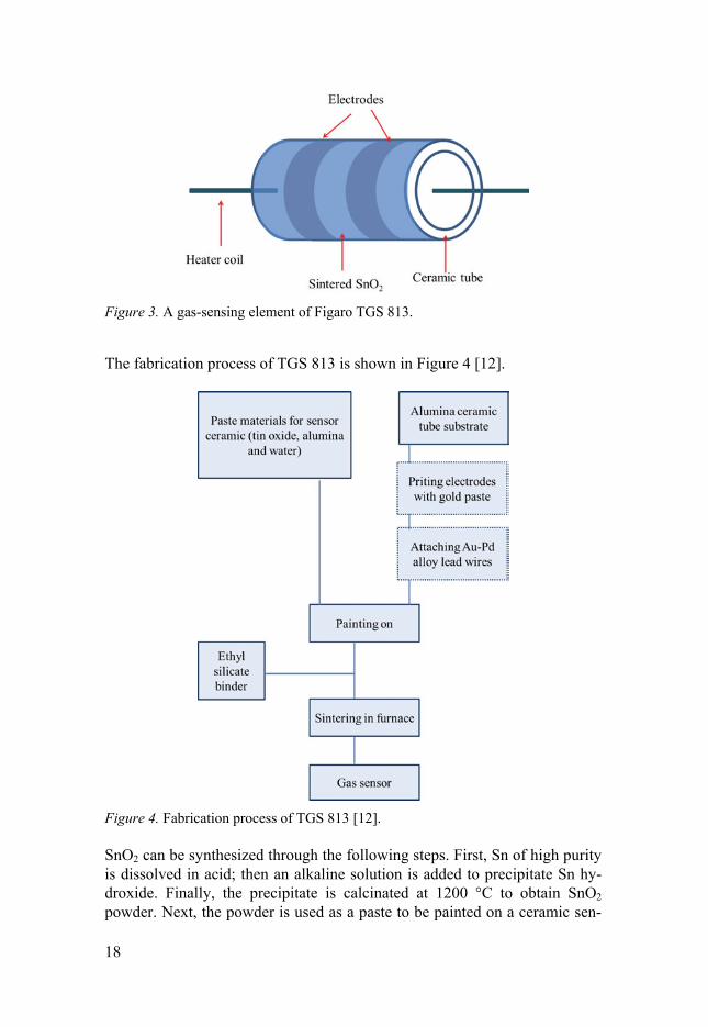
18
Figure 3. A gas-sensing element of Figaro TGS 813.
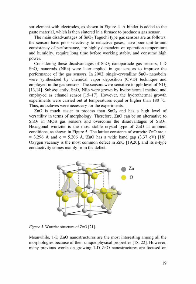
The fabrication process of TGS 813 is shown in Figure 4 [12].
Figure 4. Fabrication process of TGS 813 [12].
SnO2 can be synthesized through the following steps. First, Sn of high purity is dissolved in acid; then an alkaline solution is added to precipitate Sn hy-droxide. Finally, the precipitate is calcinated at 1200 °C to obtain SnO2 powder. Next, the powder is used as a paste to be painted on a ceramic sen-
19
sor element with electrodes, as shown in Figure 4. A binder is added to the paste material, which is then sintered in a furnace to produce a gas sensor.
The main disadvantages of SnO2 Taguchi type gas sensors are as follows: the sensors have poor selectivity to reductive gases, have poor unit-to-unit consistency of performance, are highly dependent on operation temperature and humidity, require long time before working stably, and consume high power.
Considering these disadvantages of SnO2 nanoparticle gas sensors, 1-D SnO2 nanorods (NRs) were later applied in gas sensors to improve the performance of the gas sensors. In 2002, single-crystalline SnO2 nanobelts were synthesized by chemical vapor deposition (CVD) technique and employed in the gas sensors. The sensors were sensitive to ppb level of NO2 [13,14]. Subsequently, SnO2 NRs were grown by hydrothermal method and employed as ethanol sensor [15–17]. However, the hydrothermal growth experiments were carried out at temperatures equal or higher than 180 °C. Thus, autoclaves were necessary for the experiments.
ZnO is much easier to process than SnO2 and has a high level of versatility in terms of morphology. Therefore, ZnO can be an alternative to SnO2 in MOS gas sensors and overcome the disadvantages of SnO2. Hexagonal wurtzite is the most stable crystal type of ZnO at ambient conditions, as shown in Figure 5. The lattice constants of wurtzite ZnO are a = 3.296 Å and c = 5.206 Å. ZnO has a wide band gap (3.37 eV) [18]. Oxygen vacancy is the most common defect in ZnO [19,20], and its n-type conductivity comes mainly from the defect.
Figure 5. Wurtzite structure of ZnO [21].
Meanwhile, 1-D ZnO nanostructures are the most interesting among all the morphologies because of their unique physical properties [18, 22]. However, many previous works on growing 1-D ZnO nanostructures are focused on

20
CVD technique [23]. CVD requires extremely high temperature and cannot be easily scaled up. The easiest way to obtain 1-D ZnO is by hydrothermal method [24]. An arbitrary substrate with ZnO seed layer can be put into a bottle filled with equimolar Zn(NO3)2 and (CH2)6N4 (hexamethylenetetra-mine; HMTA) and kept at 90 °C for a few hours; ZnO NRs then start to grow uniformly on the substrate [25]. The mechanism of the chemical reac-tions is described as follows [26]:
(CH2)6N4 + 6H2O ↔ 6HCHO + 4NH3 (1)
NH3 + H2O ↔ NH4+ + OH− (2)
Zn2+ + 4NH3 ↔ [Zn(NH3)4]2+ (3)
Zn2+ + 2OH− ↔ Zn(OH)2 (4)
Zn(OH)2 ↔ ZnO + H2O (5)
HMTA acts mainly as a weak base and pH buffer during NR growth [27, 28]. NH3 is a product of the decomposition of HMTA. It plays two roles in the growth process. First, it provides a basic environment for the formation of Zn(OH)2. Second, it forms a coordination complex with Zn2+ and stabiliz-es the Zn2+. As a result, ZnO NRs will be formed slowly in the aqueous solu-tion.
In this study, an ultrathin seed layer of Zn on a silicon or glass substrate is made by sputtering for the ZnO nanostructures to grow on. The Zn layer is naturally oxidized into a ZnO layer before the solution growth of NRs [29]. The obtained ZnO NRs or nanowires (NWs) are all of hexagonal type. The morphologies of the 1-D ZnO nanostructures can be tuned by adjusting the growth parameters, specifically, precursor concentration, growth tempera-ture, growth time, and growth pressure. As discussed in [30], the easiest way to grow thin ZnO NWs is by lowering precursor concentration, which should be ≤0.005 M to achieve ultrathin secondary NWs. Growth temperature should be ≥90 °C, and the time should be sufficiently long, usually longer than 16 h. The growth pressure can be kept at atmospheric condition.
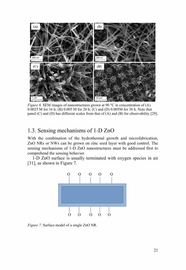
Figure 6 shows the ZnO NWs grown on the Zn seed layer on silicon sub-strates. Notably, Figure 6D shows that the ZnO NWs are grown with site selectivity. This growth can be realized by microfabrication technique, which will be discussed in the experimental part.
21
Figure 6. SEM images of nanostructures grown at 90 °C in concentration of (A) 0.0025 M for 16 h; (B) 0.005 M for 20 h; (C) and (D) 0.005M for 36 h. Note that panel (C) and (D) has different scales from that of (A) and (B) for observability [29].
1.3. Sensing mechanisms of 1-D ZnO With the combination of the hydrothermal growth and microfabrication, ZnO NRs or NWs can be grown on zinc seed layer with good control. The sensing mechanisms of 1-D ZnO nanostructures must be addressed first to comprehend the sensing behavior.
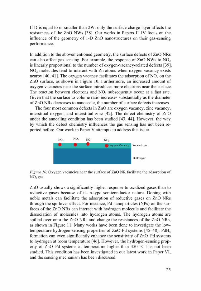
1-D ZnO surface is usually terminated with oxygen species in air [31], as shown in Figure 7.
Figure 7. Surface model of a single ZnO NR.

22
The types of oxygen species adsorbed are determined by the environmental temperature. When measurement temperature is larger than 300 °C, O2- is the dominating ion [32]. 1. O2 (g) O2 (ads) (Physical adsorption) 2. e-+O2 (ads) O2
- (Ionic adsorption; < 100 °C) 3. 2e-+ O2
- 2O- (Ionic adsorption; 100-300 °C) 4. e-+ O- O2- (Ionic adsorption; > 300 °C)
After ionic adsorption of the oxygen species, the electrons originating from donor sites (for example, intrinsic oxygen vacancies) are extracted from the conduction band and trapped at the surface of the ZnO NR. These processes produce electron-depleted surface region, which is the so-called surface charge layer with thickness W, as shown in Figure 8. Notably, the negative surface charge results in the surface band bending, which generates a surface potential barrier eVsurface. The height of this barrier and depth of the band bending depend on the amount and type of the adsorbed oxygen ions.
Figure 8. Schematic diagram of band bending after chemisorption of charged spe-cies (in this case, O-) EC, EV, and EF denote the energy of the conduction band, va-lence band, and the Fermi level, respectively, while W denotes the thickness of the space-charge layer, and eVsurface denotes the potential barrier (adopted from [33]). The conducting electrons are represented by e– and + represents the donor sites.
Here the thickness of the surface charge layer can be expressed as W = (6)

23
where ϵ is the relative permittivity of the metal oxide, ϵ is the dielectric constant of vacuum and equals to 8.85×10⁻¹² F/m, V is the band bending, q is the elementary electron charge and equals to 1.6×10⁻¹⁹ C, and n is the charge carrier density [34].
Considering some typical values of ZnO reported from the literature, n is approximately 5×1017 cm-3 [35], ϵ about 8 [20], and qV about 0.5 eV [36], W can be estimated to be about 30 nm. When the diameter of ZnO NWs is equal to or smaller than 2W, the adsorption and desorption of oxy-gen will influence the entire ZnO NWs. As a result, the ZnO NWs will be highly sensitive to target gases
Increase in the thickness of the surface charge layer can lead to a small conduction channel and thus contribute to the large resistance of ZnO NRs. When oxidizing gases are adsorbed onto the surface of the ZnO NRs, they attract more electrons from the surface. The thickness of surface charge layer increases. Thus, the resistance of the ZnO NRs increases. When reducing gases are present, they react with O2- and release electrons to the surface charge layer. Thus, the resistance of ZnO NRs decreases.
The surface charge layer thickness W depends on the Debye length LD, which is a characteristic parameter of semiconductor materials for a particu-lar charge carrier density [33]. In this context, the Debye length can be ex-pressed by Equation (6) [37]: L = (7)
where is the Boltzmann constant and equals to 1.38×10⁻²³ J/K. As shown in Equation (7), LD is temperature dependent. Considering some typical val-ues of ZnO from reported literature, n and ϵ of the value mentioned above, the typical Debye Length is approximately 8 nm at T of about 673 K.
The comparison of Equations (6) and (7) shows that the surface charge layer thickness of the ZnO NR can be expressed in Equation (8).
W = L (8)

24
However, in this thesis, the sensing materials are mostly ZnO NR networks, which possess multiple junctions instead of a single standalone ZnO NR. Thus, a contact barrier exists between the two ZnO NRs, as shown in Figure 9. In this case, both the contact barriers (band bending) and surface charge layers of the ZnO NRs can influence gas sensing. The surface charge layer also affects band bending.
Figure 9. Structural and band model showing the role of contact regions of ZnO NRs in determining the conductance over the layer of ZnO NRs (adapted from [33])
Three cases can happen depending on the diameter (D) of ZnO NRs and the thickness of the surface charge layer [37].
If D is significantly larger than 2W, the surface charge layer has little ef-fect on the resistance of ZnO NRs. However, the surface charge layer signif-icantly influences the contact barrier. Gas sensing is controlled by the con-tact barrier between the two ZnO NRs. Moreover, the contact barrier is inde-pendent from the diameter of the ZnO NRs. The sensitivities of the ZnO NRs are not influenced by their diameters. In this case, the layer conduct-ance of the ZnO NR network can be described by Equation (9) [24,36]. = exp − (9)
If D is slightly larger than 2W, the surface charge layer affects the resistance of ZnO NRs and contact barrier between the ZnO NRs. Thus, gas sensing depends on both the contact barriers and sizes of the ZnO NRs.
25
If D is equal to or smaller than 2W, only the surface charge layer affects the resistances of the ZnO NWs [38]. Our works in Papers II–IV focus on the influence of the geometry of 1-D ZnO nanostructures on their gas-sensing performance.
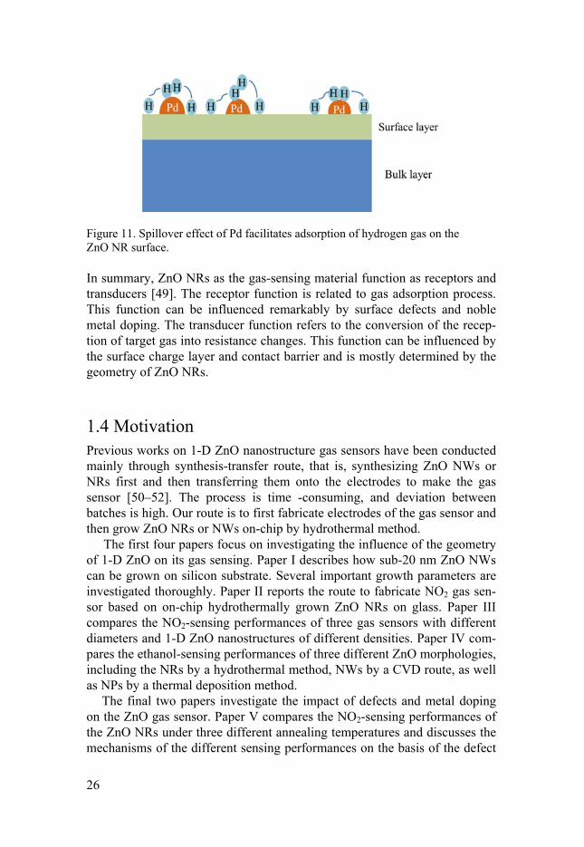
In addition to the abovementioned geometry, the surface defects of ZnO NRs can also affect gas sensing. For example, the response of ZnO NWs to NO2 is linearly proportional to the number of oxygen-vacancy-related defects [39]. NO2 molecules tend to interact with Zn atoms when oxygen vacancy exists nearby [40, 41]. The oxygen vacancy facilitates the adsorption of NO2 on the ZnO surface, as shown in Figure 10. Furthermore, an increased amount of oxygen vacancies near the surface introduces more electrons near the surface. The reaction between electrons and NO2 subsequently occur at a fast rate. Given that the surface to volume ratio increases substantially as the diameter of ZnO NRs decreases to nanoscale, the number of surface defects increases.
The four most common defects in ZnO are oxygen vacancy, zinc vacancy, interstitial oxygen, and interstitial zinc [42]. The defect chemistry of ZnO under the annealing condition has been studied [43, 44]. However, the way by which the defect chemistry influences the gas sensing has not been re-ported before. Our work in Paper V attempts to address this issue.
Figure 10. Oxygen vacancies near the surface of ZnO NR facilitate the adsorption of NO2 gas.
ZnO usually shows a significantly higher response to oxidized gases than to reductive gases because of its n-type semiconductor nature. Doping with noble metals can facilitate the adsorption of reductive gases on ZnO NRs through the spillover effect. For instance, Pd nanoparticles (NPs) on the sur-faces of the ZnO NRs can interact with hydrogen molecule and facilitate the dissociation of molecules into hydrogen atoms. The hydrogen atoms are spilled over onto the ZnO NRs and change the resistances of the ZnO NRs, as shown in Figure 11. Many works have been done to investigate the low-temperature hydrogen-sensing properties of ZnO-Pd systems [45–48]. PdHx formation can even significantly enhance the sensitivity of ZnO–Pd systems to hydrogen at room temperature [46]. However, the hydrogen-sensing prop-erty of ZnO–Pd systems at temperature higher than 350 °C has not been studied. This condition has been investigated in our latest work in Paper VI, and the sensing mechanism has been discussed.
26
Figure 11. Spillover effect of Pd facilitates adsorption of hydrogen gas on the ZnO NR surface.
In summary, ZnO NRs as the gas-sensing material function as receptors and transducers [49]. The receptor function is related to gas adsorption process. This function can be influenced remarkably by surface defects and noble metal doping. The transducer function refers to the conversion of the recep-tion of target gas into resistance changes. This function can be influenced by the surface charge layer and contact barrier and is mostly determined by the geometry of ZnO NRs.
1.4 Motivation Previous works on 1-D ZnO nanostructure gas sensors have been conducted mainly through synthesis-transfer route, that is, synthesizing ZnO NWs or NRs first and then transferring them onto the electrodes to make the gas sensor [50–52]. The process is time -consuming, and deviation between batches is high. Our route is to first fabricate electrodes of the gas sensor and then grow ZnO NRs or NWs on-chip by hydrothermal method.
The first four papers focus on investigating the influence of the geometry of 1-D ZnO on its gas sensing. Paper I describes how sub-20 nm ZnO NWs can be grown on silicon substrate. Several important growth parameters are investigated thoroughly. Paper II reports the route to fabricate NO2 gas sen-sor based on on-chip hydrothermally grown ZnO NRs on glass. Paper III compares the NO2-sensing performances of three gas sensors with different diameters and 1-D ZnO nanostructures of different densities. Paper IV com-pares the ethanol-sensing performances of three different ZnO morphologies, including the NRs by a hydrothermal method, NWs by a CVD route, as well as NPs by a thermal deposition method.
The final two papers investigate the impact of defects and metal doping on the ZnO gas sensor. Paper V compares the NO2-sensing performances of the ZnO NRs under three different annealing temperatures and discusses the mechanisms of the different sensing performances on the basis of the defect

27
theory. Paper VI studies ZnO NRs with three different thickness of palladi-um by sputtering. The three different samples are compared. The origin of different sensing performance is examined.
In summary, investigations of both the transducer and receptor function of 1-D ZnO in gas sensors have been carried out in this thesis. Special efforts have been focused on the evaluation of important factors that determine the sensitivity, selectivity, and stability of the 1-D ZnO gas sensors.

28
2. Experimental
2.1 Fabrication of gas sensor devices The ZnO gas sensors are fabricated through the combination of microfabri-cation and hydrothermal method. MOS gas sensors usually have three com-ponents, that is, heater, electrode, and metal oxide. The normal route is to make the electrodes first, and then transfer the metal-oxide material onto the electrodes, and finally, integrate the heater. In this study, electrodes and the heater can be made simultaneously through microfabrication. A Zn seed layer in the form of small islands is deposited on and between the electrodes for later hydrothermal growth. The ZnO nanostructures were obtained through on-chip growth instead of transferring. This route can improve the reliability of the gas sensing and decrease unit-to-unit deviation. Further-more, the cost of the gas sensors can be decreased through batch production.
2.1.1 Microfabrication Microfabrication technique usually has four categories: patterning, deposi-tion, removal, and bonding. Patterning is usually performed through photoli-thography, in which a UV lamp is used as light source. The process is shown in Figure 12.

29
Figure 12. Schematic diagram of photolithography.
Photoresist is a UV-sensitive polymer. After UV exposure through a mask and development, the photoresist forms a pattern. The patterned photoresist covers a specific area of the substrate, which is not affected by the next dep-osition or etching step. A photoresist can withstand most acidic conditions, such as HF, HCl, and H3PO4. However, it is dissolved by a strong base solu-tion, such as KOH.
Deposition adds a new layer of a material onto the substrate. Physical va-por deposition (PVD) and CVD are the commonly used deposition tech-niques.
PVD is a process in which the source material goes from a solid or liquid phase to a vapor phase and then reaches the substrate, where the source ma-terial condenses to form a thin film [53]. The two most common PVD pro-cesses are sputtering and evaporation.
Sputtering is a process whereby surface atoms are ejected from a solid source material, called target, because of the bombardment of the target by energetic particles, normally argon gas ions [54]. The process is shown in Figure 13.

30
Figure 13. Schematic diagram of sputter [55].
Evaporation is a PVD process in which a hot source material evaporates and then reaches the substrate with little or no collision with gas molecules in the space between the source and substrate [54]. The heat element can be either resistance or electron-beam, depending on the melting point of the source material. Platinum, for example, has a high melting point of 1768.2 °C; therefore, an electron beam should be used. The equipment is shown in the schematic diagram in Figure 14.
Figure 14. Schematic diagram of evaporation deposition [56].
The evaporation process requires considerably higher vacuum than the sput-tering process. In our projects, sputtering and evaporation are both used for depositing metal layers. Notably, sputtering can also be used to sputter metal oxides. After sputtering, the wafer with metal on photoresist is lifted off in
31
three acetone baths and one isopropanol bath sequentially. The procedure is therefore called a lift-off process.
The thickness and roughness of the deposited film is important to semi-conductor devices. Stylus profilometry and atomic force microscopy (AFM) are the common tools used to examine thin films. In Paper I, AFM is used to examine the roughness and thickness of the Zn seed layer. Stylus profilome-try is used in all the other works to check the thickness of the electrode layer.
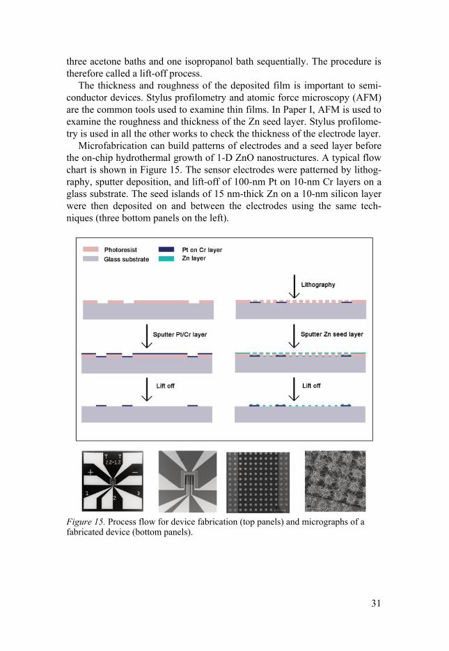
Microfabrication can build patterns of electrodes and a seed layer before the on-chip hydrothermal growth of 1-D ZnO nanostructures. A typical flow chart is shown in Figure 15. The sensor electrodes were patterned by lithog-raphy, sputter deposition, and lift-off of 100-nm Pt on 10-nm Cr layers on a glass substrate. The seed islands of 15 nm-thick Zn on a 10-nm silicon layer were then deposited on and between the electrodes using the same tech-niques (three bottom panels on the left).
Figure 15. Process flow for device fabrication (top panels) and micrographs of a fabricated device (bottom panels).

32
2.1.2 Growth of 1-D ZnO nanostructures After patterning, the chip is put upside down in a premixed equimolar solu-tion of Zn(NO3)2 and HMTA and kept there for a few hours. 1-D ZnO nanostructures with different diameters and densities can be obtained by adjusting growth parameters, such as precursor concentration, temperature, pressure, and time. ZnO NR networks can be obtained from a two-step growth process using a precursor at a relatively high concentration, whereas a ZnO NW network is obtained also from a two-step growth process with precursor at low concentration. The growth temperature influences the as-pect ratio of the ZnO nanostructures. The higher the temperature is, the larg-er the aspect ratio is. The ZnO nanostructures are usually grown at tempera-tures higher than 80 °C. The growth time influences the length of ZnO nanostructures. It is usually longer than 16 h. Considering that the concentra-tion of the precursor will be extremely low after 16 h in the first step; the second step is needed to develop the secondary NWs or NRs long enough to contact each other. All of the growth experiments are carried out at atmos-pheric pressure without autoclave.
2.2. Characterization of ZnO Nanostructures Seven measurement techniques have been applied to examine the ZnO nanostructures. Optical microscopy can examine the electrodes of the gas sensors and the overall density of the ZnO nanostructures. Scanning electron microscopy (SEM) can examine the morphologies of the ZnO nanostructures. Energy-dispersive X-ray spectroscopy in SEM can examine the element information of the ZnO nanostructures as well. Transmission electron mi-croscopy (TEM) examines the distribution and the crystal type of PdO NPs on the ZnO NRs. X-ray diffraction (XRD) examines the crystal type of the ZnO nanostructures. Photoluminescence spectroscopy has been applied to examine the defects near the surface of ZnO NRs. X-ray photoelectron spec-troscopy (XPS) has been applied to examine the surface chemical infor-mation of ZnO-Pd systems. The basic principles of these techniques are pro-vided below.
2.2.1 Optical Microscopy After hydrothermal growth, the gas sensor must be examined under an opti-cal microscope, which has limited resolution (half of the light wavelength, 200 nm) because of the visible light source. Despite this limitation, optical microscope can be conveniently used to determine whether the gas sensor works or not. The electrodes of the gas sensor must be intact. The ZnO NRs or NWs between the electrodes have to be connected to each other to form

33
an electrical path. Bright mode and dark mode were combined to obtain more information of our samples.
2.2.2 SEM with EDS Considering that the diameters of our nanomaterial are typically less than 300 nm, SEM is an indispensable tool to characterize our ZnO nanostruc-tures. In SEM, an electron beam scans over the surface of the sample and yields an image of the surface of the sample. The resolution is approximately 10 nm. Figure 16 shows the interaction volume between the specimen and incidence electron beam. SEM images are usually formed based on second-ary electrons, which are surface sensitive. In addition, element analysis can be done locally using an EDS detector. The analysis volume of EDS in SEM is large, and the depth ranges from 0.1 to 3 microns, depending on the accel-eration voltage. SEM requires the specimen to be conductive. Thus, the ZnO samples must be sputtered with a thin Pd–Au layer to increase the conductiv-ities of the samples. The gas-sensing performances of the ZnO nanostruc-tures are measured first before SEM, because the sputtered Pd–Au layer alters or terminates the sensing performance of the sensor. SEM has been used in all of the studies presented in this work to examine the morphologies of the ZnO nanostructures. EDS has been used in Paper VI to compare Pd-doped ZnO NR sample with the non-doped one in a quantitative manner.
Figure 16. Interaction volumes between incidence electron beam and bulk specimen in SEM [57].

34
2.2.2 TEM Generally, SEM is used for the examination of bulk material, whereas TEM for thin specimen. Interaction between the incidence electron beam and thin specimen is shown in Figure 17 [58].
Figure 17. Interaction volume between incidence electron beam and thin specimen in TEM [58].
Three types of transmitted electrons are commonly used in TEM to obtain information on the specimen. The functions of the three types of electrons are listed below [58].
Unscattered electrons: Incident electrons are transmitted through the spec-imen without any interaction. The transmission is inversely proportional to the thickness. A thick area will appear dark, whereas a thin area will have more transmitted electrons and thus will appear light.
Elastically scattered electrons: Incidence electrons are scattered by atoms in the specimen without energy loss. They can yield information about the orientation, atomic arrangements, and phase present in the area being exam-ined.
Inelastically scattered electrons: Incidence electrons interact with atoms and lose energy during the interaction. They can be used to extract both compositional and bonding information on the examined specimen region.
2.2.3 XRD XRD can be used to analyze the crystallography information of ZnO. The basic principle is based on Bragg’s law:

35
2dsin θ= nλ
where d is the spacing between diffracting planes, Ɵ is the incident angle, n is any integral, and λ is the wavelength of the beam [59]. In our experiment, Cu Kα radiation was used, and λ is 1.54184Å. According to Bragg’s Law, the spacing between diffracting planes can be determined if the incident angle is known. Different crystal plane of the grown ZnO nanostructures can be de-termined. XRD has been used in most of the papers in this thesis. For ZnO NWs grown on silicon substrate in Paper I, Grazing Incidence XRD has been used to minimize the signal from the underlying silicon substrate and obtain more information on ZnO NWs.
2.2.4 Photoluminescence (PL) PL is a nondestructive technique for the detection of defects in semicon-
ductors. Both shallow-level and deep-level defects can be detected, provided that the recombination between the deep-level defects is radiative [60]. However, the PL signal is highly sensitive to surface defect recombination.
The following are the five of the most commonly observed PL transitions: 1) band-to-band recombination (Figure 18a), 2) excitonic recombination (Figure 18b), 3) bound exciton (BE) recombination (Figure 18c), 4) free electron recombine with a hole on a neutral acceptor (Figure 18d), and 5) donor–acceptor (D-A) recombination (Figure 18e). A detailed description can be found in [60]. Light emission from the recombination reveals the defect types in the examined bulk material. ZnO may have several types of defects (i.e., vacancy and interstitial of oxygen and zinc) near the surface. Thus, PL is an important tool to probe the surface defects states, as discussed in Paper V.
Figure 18. Radiative transitions observed with PL [60].

36
2.2.5 XPS X-ray Photoelectron Spectroscopy (XPS) was first known as ESCA (Elec-tron Spectroscopy for Chemical Analysis) [61]. It is a powerful tool to inves-tigate chemical information from material surface at a depth of 10 nm. The element type, the chemical states of the element, and the quantity of the ele-ment in the surface region can all be obtained from XPS spectra. The surface analysis by XPS is accomplished by irradiating a sample with monochro-matic soft X-rays, and then analyzing the energy of the detected photoelec-trons [62]. In our works, Al Kα X-ray with energy of 1486.7 eV is used. The measured kinetic energy of the emitted electron is given by
Ekinetic = Ephoton – (Ebinding + Φ)
where Ephoton is the energy of the X-ray photon, Ebinding is the binding energy of the electron, and Φ the spectrometer work function [62].
In Paper VI, XPS is used to investigate the amounts and chemical states of sputtered Pd film on ZnO NRs.
2.3 Gas sensing characterization The gas sensors are tested with flow-through technique [63]. Switching be-tween dry air and test gas takes approximately 1 s. In the experiment, the standard gas is mixed with dry air as carrier. This process uses several mass flow controllers, as shown in Figure 19. The standard gas is composed of the target gas balanced with pure nitrogen. The concentration of the standard gas is usually 1% or 1000 ppm. The flow rates of the standard gas and dry air are varied, and test gases with low concentrations are obtained. Before the sens-ing measurement, dry air flows through the sensing chamber until a stable sensor resistance is obtained. The resistance of the sensors is continuously measured by using a Keithley SourceMeter (Model 2700) and sampled using a computer. The dry air and the test gas are switched on and off each cycle.

37
Figure 19. Gas sensor test system, reproduced from [64].
Two different measurement systems are used in the projects: one automatic measurement system for NO2 gas, the other is a semi-automatic measure-ment system for reductive gas (hydrogen, ammonia, and ethanol). Before the automatic measurement of NO2 gas, a test run is performed to determine the response and recovery period at the low concentration. The value is then inputted in the measurement program. The program for NO2 test automati-cally switches the test gases or dry air on and off according to the input time, while the dynamic resistances of the sensor are recorded continuously. For reductive gas, a test run is also required to determine response and recovery period. However, switching the gases on and off is performed manually while the program continuously acquires the resistance data. Therefore, the response and recovery time is more accurate at low concentrations of test gas than at high concentrations. The reason is that the latter requires longer time than the former. The automatic program does not wait longer than the input time for switching.
The sensors are placed on a heater chuck during the gas measurement, even though the heaters are integrated on the sensor chip. Two reasons can explain this condition. On the one hand, the external heater is more stable and uniform than the heater on the chip, given that a thermal drop occurs on the chip when the heater on the chip is used. On the other hand, the external heater facilitates the comparison of different sensors at the same operation temperature. All of the measurements are carried out with the external heater.

38
The ZnO sensors are tested at temperature higher than 200 °C considering the adsorption barrier of test gases and humidity. Most of the measurements are performed at temperatures of 350, 400, and 450 °C. The influence of humidity is negligible.
In this thesis, the sensor response is defined as Rgas/Rair or Rgas/Rair. Rair is the resistance of the sensor in the dry air, and Rgas is the resistance of the sensor when the test gas is introduced. Response time is defined as the time required to arrive 90% of full response from the base line to the saturated response. Accordingly, recovery time is also defined as the time required to arrive 90% of decrease from the saturated response to the base line, as shown in Figure 20.
Figure 20. Dynamic resistance changes of ZnO NWs during one measurement cycle, concentration of NO2 gas is 2.5 ppm.
Sensitivity in this thesis is defined as response divided by the concentration of the test gas. Given that different studies may measure the same gas at different concentrations, sensitivity can be used to compare the sensor per-formances. Notably, in several publications, including Paper II in this study, sensitivity is defined in the same way as response, and this definition is mis-leading. Selectivity is defined as the ratio between the responses of the sen-sor to two different gases at same concentration and measurement conditions.
Selectivity = Response1 / Response2.

39
3. Summary of results
3.1 Summary of Paper I Paper I describes the method to synthesize ultrathin secondary ZnO NWs on silicon substrate. In the first step, an ultrathin Zn layer is deposited on the substrate. This active metal is oxidized to ZnO before hydrothermal growth of NWs. In the second step, ultrathin ZnO NWs are grown at 90 °C for 16 h or longer using 0.005-M precursor solution of Zn(NO3)2 and HMTA. Low temperature and atmospheric pressure growth make the method promising for batch production of ZnO NWs. The mechanism of the growth of ultrathin ZnO NWs is illustrated in Figure 21. Ultrathin ZnO NWs is formed through three steps. First, a dense layer of ZnO NRs is formed on the thin ZnO seed layer. Second, sharp tips and secondary seeds are formed. Third, ultrathin secondary NWs grow from the tips of the primary ZnO NRs. Notably, the ultrathin secondary ZnO NWs can site-selectively grow on silicon substrates using isolated islands of Zn seed layer.
Figure 21. Proposed mechanism for the growth of ultrathin ZnO NWs from formation of big ZnO NRs from seed layer to nucleation and growth of secondary ultrathin ZnO NWs from the tips of the NRs [29].

40
3.2 Summary of Paper II NO2 sensors based on ZnO nanostructures are built on a glass substrate. As shown in Figure 22, ZnO NRs are connected to one another in the two steps. In the first step, short NRs grow on the seed sites after 4 h. In the second step, long NRs grow continuously from short NRs. After the two steps, NRs are sufficiently long to make contact with each other, as shown in Figures 22D and 23B. The NRs are quite porous, and this condition is good for gas sens-ing, as shown in Figure 23C. The measurements show that the ZnO NR gas sensors performed best at 450 °C. Moreover, the sensors are more sensitive to NO2 than the other reductive gases.
Figure 22. Formation of ZnO NRs junctions by two-step hydrothermal growth: (A) deposition of Pt electrodes; (B) deposition of Zn seed islands; (C) growth of dense ZnO nanorods (first step); (D) growth of long porous ZnO nanorods (second step) [63].

41
Figure 23. Material characterizations of ZnO NRs synthesized with hydrothermal method at 85 °C: (A) SEM image of ZnO NRs within Pt electrodes, (B) higher mag-nification of ZnO NRs grown from different islands making NR junctions, (C) im-age of a single ZnO NR, (D) X-ray diffraction of the ZnO NRs [63].
3.3 Summary of Paper III In Paper II, on-chip grown ZnO NRs show good response to NO2. Neverthe-less, the sensitivity is not as high as those reported by other works on similar ZnO nanostructures. In the present case, sensitivity is used to compare our work with others. In Paper III, a comparative study of three ZnO 1-D nanostructures is conducted. ZnO NWs with high sensitivity to NO2 are syn-thesized by on-chip hydrothermal method.
The three ZnO nanostructures are ZnO NRs, dense ZnO NWs, and sparse ZnO NWs. They have different geometries and densities, although they have the same crystal type. The diameters of the ZnO NRs range from 150 nm to 200 nm, as shown in Figure 24A. Dense ZnO NWs have a diameter of ap-proximately 25 nm to 50 nm, as shown in Figure 24B. The diameters of sparse ZnO NWs are less than 25 nm.

42
Figure 24. SEM images of the three ZnO nanostructures: (A) ZnO-NRs, (B) dense ZnO NWs, and (C) sparse ZnO NWs. The scale bar is 1 μm. The insets are magnifi-cations of the respective images with scale bar of 100 nm.
The highest sensitivity of ZnO NWs is nearly 6 per ppm, as shown in Table 4. This value is significantly higher than those of ZnO nanoarrays synthe-sized at 95 °C. Moreover, the ZnO NWs have comparable sensitivity with those of ZnO nanostructures synthesized at temperature higher than 100 °C.
Table 4. Comparison of the best sensing performances of the three ZnO samples to 2.5 ppm NO2.
Sample Optimum work Temperature (°C)
Response time (s)
Recovery time (s)
Response
ZnO-NRs 350 226 264 1.96
Dense ZnO NWs 350 113 169 4.1
Sparse ZnO NWs 300 52 101 14.92
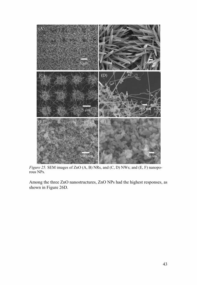
3.4 Summary of Paper IV In Paper IV, three ZnO nanostructures with different morphologies are tested toward ethanol. ZnO NRs are grown by on-chip hydrothermal method on a thermally oxidized silicon chip. ZnO NWs are prepared by on-chip chemical vapor deposition method, while the ZnO NPs through the thermal deposition of sheet-like hydrozincite at 400 °C. As shown in Figure 25B, ZnO NRs each have a diameter of approximately 250 nm. ZnO NWs each have a width of around 80 nm, as shown in Figure 25D. ZnO NPs have an average size of about 30 nm, as shown in Figure 25F.
43
Figure 25. SEM images of ZnO (A, B) NRs, and (C, D) NWs; and (E, F) nanopo-rous NPs.
Among the three ZnO nanostructures, ZnO NPs had the highest responses, as shown in Figure 26D.

44
Figure 26. Transient resistance versus time upon exposure to different ethanol concentrations of fabricated sensors: (a) NRs, (b) NWs, (c) NPs, and (d) sensor response as a function of ethanol concentration
3.5 Summary of Paper V In Paper V, on-chip hydrothermally grown ZnO NRs are annealed at either at 400, 500, or 600 °C. The crystal structures and defect emissions of ZnO NRs before and after each annealing are examined by XRD and PL Spec-troscopy. No evident change in crystal structure is observed. However, de-fect emissions are considerably changed. Three peaks are examined in PL (Figure 27). The peak centered at 380 nm is related to exciton recombination in ZnO surface. The peak centered at 550 nm corresponds to the recombina-tion of electrons in the conduction band with oxygen vacancy. The peak centered at 610 nm is referred to interstitial oxygen defects.
When annealing temperature increases from 400 °C to 600 °C, the num-ber of oxygen vacancies decreases and that of interstitial oxygen increases near the ZnO surface.

45
Figure 27. PL of ZnO NRs before and after annealing.
Unannealed ZnO NRs show the highest response among all the samples, but the sample is not stable. In addition, it is annealed while being measured so that the result is not repeatable. ZnO NRs_400 °C exhibits the highest re-sponse to NO2 among the three annealed samples, as shown in Figure 28. However, ZnO NRs_400 °C is unstable after 1 week in air (Figure 29). ZnO NRs_600 °C show low response to NO2 but demonstrate high stability after 1 week in air.
Figure 28. Response of the ZnO NRs to NO2 at different temperatures: (A) unan-nealed, (B) annealed at 400 °C, (C) annealed at 500 °C, (D) annealed at 600 °C.

46
Figure 29. Response of the ZnO NRs to 10 ppm NO2 in 10 cycles measured at 350 °C: (A) ZnO at 400 °C, (B) ZnO at 600 °C.
The different sensing properties of ZnO NRs annealed at different tempera-tures are due to defects reactions as shown below [43]:
1/2O2 + 2e− = O2−, (9) 1/2O2 + VO = OO, (10) 1/2O2 = OO + VZn, (11)
1/2O2 + Zni = OO + ZnZn, (12) 1/2O2 = Oi, (13)
where OO and ZnZn refer to the neutrally charged oxygen and zinc at the crystal lattice site. Oxygen diffusion in the ZnO NRs can eliminate VO and Zni, as shown in Equations (10) and (12), and it can also increase VZn and Oi, as shown in Equations (11) and (13), respectively.
3.6 Summary of Paper VI In this work, 2, 4, and 8 nm-thick Pd layers are sputtered on the on-chip hy-drothermally grown ZnO NRs to improve hydrogen sensing at high tempera-ture. Before the gas test, the ZnO NRs are annealed at 650 °C, and the Pd is oxidized into PdO. The crystal direction of PdO cluster is <101> (Figure 30F).

47
Figure 30. SEM images of ZnO NRs: (A) overall image of the on-chip grown ZnO NRs, (B) ZnO NRs without Pd, (C) ZnO NRs with 4 nm Pd, and (D) ZnO NRs with 8 nm Pd. HRTEM images of the ZnO-Pd 4 nm sample: (E) low magnification, and (F) high magnification
Pristine ZnO has low response to hydrogen, as depicted in Figure 31E. ZnO-Pd 2 nm sample has the highest response to hydrogen at 450 °C. The re-sponse of the 2 nm ZnO-Pd sample to 1,000-ppm hydrogen is 8.23 (Figure 30F). The response of ZnO-Pd 2 nm to hydrogen increases with measure-ment temperature. By contrast, the response of ZnO-Pd 4nm to hydrogen with measurement temperature tends to decrease. The response increases as the temperature decreases from 450 °C to 350 °C, and the highest value is 6 (Figure 31G). The ZnO-Pd 8 nm exhibits a sensing behavior opposite to those of the other three. The resistance of the sample increases as hydrogen is introduced, as shown in Figure 31D.

48
Figure 31. Typical dynamic transient response at 450 oC (A-D) and gas response as a function of gas concentration (E-H) of pristine ZnO NRs (A, E), ZnO-Pd 2 nm (B, F), ZnO-Pd 4 nm (C, G), ZnO-Pd 8 nm (D, H).
The mechanisms underlying the different sensing behaviors are explained by the spillover effect and Pd–Zn alloy formation at high temperatures. Pd–Zn alloy formation enhances the spillover effect but decreases the amount of ZnO. The ZnO-Pd 2nm exhibits low spillover effect on hydrogen at 350 °C. At high temperatures, the number of Pd reduced from the PdO is increased in ZnO-Pd 2 nm sample, to ensure that the spillover effect is enhanced. The Pd–Zn alloy is formed and thus consumes a part of the ZnO NRs. However, owing to the small amount of Pd, the ZnO consumption does not result in any large nega-tive effect on sensing performance. The ZnO-Pd 4nm sample exhibits high spillover effect at 350 °C because of the sufficient amounts of Pd. However, at 450 °C, the amount of Pd–Zn alloys increases at the cost of the ZnO material. As a result, the response decreases at increasing temperature. When the Pd layer is extremely thick, as in the case of the ZnO-Pd 8 nm sample; it forms a large amount of Pd–Zn alloy in the ZnO NRs at high temperatures. The base resistance of the sensor decreases two orders of magnitude relative to that of undecorated ZnO (Figure 31D). In this case, Pd forms a continuous layer be-tween the electrodes in ZnO-Pd 8nm sensor. Therefore, the ZnO-Pd 8 nm exhibits reverse and low response compared with the other ZnO-Pd samples.

49
Figure 32. Sensing mechanism of the ZnO NR-Pd sensors at high temperature.

50
Conclusion and outlook
The studies in this thesis explored the transducer function and receptor func-tion of 1-D ZnO in gas sensors. On the basis of all the results presented thus far, the following conclusions can be drawn: 1) Ultrathin secondary ZnO NRs can be hydrothermally grown on silicon substrate at times longer than 16 h at 90 °C using 0.005-M precursor solution of Zn(NO3)2 and HMTA. 2) Two-step grown ZnO NRs have good sensitivity and selectivity to NO2. 3) Sparse ZnO NWs have the highest sensitivity to NO2 among all the hydro-thermally grown 1-D ZnO samples. 4) ZnO NPs possess high sensitivity to ethanol because of its small size and large surface area; 5) Annealing in air influences oxygen vacancy near the surface of ZnO NRs, thus affecting the sensitivity and stability of ZnO NRs. 6) Pd-Zn alloy formed at high tempera-tures has harmful effects on the gas sensing performances of ZnO NRs. Therefore, the thickness of sputter-deposited Pd should be optimized. Gas sensors based on on-chip hydrothermally grown 1-D ZnO nanostruc-tures have been fabricated, decorated, tested, and stabilized. Nevertheless, many other studies may be carried out in future work. The following are examples of these studies: 1) Different ZnO morphologies can be obtained by on-chip hydrothermal growth. The growth of crystal is determined by the surface energy of each crystal plane. Through the addition of some specific surfactant, some crystal planes of ZnO can be inhabited during solution growth. Selectivity for the reductive gases, such as ethanol or ammonia, can be enhanced when the crystal plane are well controlled during the hydrothermal growth. 2) Oxygen vacancy at the surface should be controlled to increase stability. The best approach is to add another surface layer to remove oxygen from ZnO and stabilize the oxygen vacancy at the interface. If an nm-thick Al2O3 can be deposited on the surface of ZnO NWs with conformity, both the sen-sitivity and stability of ZnO NWs should be increased. 3) Combination of ZnO nanostructures and catalytic metals are of great in-terest for selective gas sensing. Some common catalytic metals are Cu, Ni, Pd, and Pt. More exotic system should be explored to enhance not only gas response and but also selectivity at high temperatures.

51
4) ZnO NWs based on room-temperature sensor is interesting. When the diameter of ZnO NWs decreases, their surface volume ratio increases, and defects near the surface per volume unit increases as well. Given that oxygen defects on the surface increases the reactive sites for NO2, ZnO may be used to sense NO2 at room temperature. Nevertheless, humidity is expected to have a significant influence on ZnO gas sensing at room temperature.

52
Sammanfatting På Svenska
Gassensorn, patenterad redan 1941, användes för mätning av luftens fuktig-het. Vattenånga är bara en av de gaser som finns i luften. Några av dem har karakteristiska lukter och kan därmed upptäckas med luktsinnet, medan andra är luktfria och farliga. Ett problem med luktsinnet är att det inte kan bestämma koncentrationer av gaserna och att man vänjer sig vid en viss lukt. Det är situationen då man befinner sig i en (svagt) luktande miljö och efter en stund känner man inte av den lukten längre, eller åtminstone inte så mycket av den som i början. En gassensor ska fungera så att den kan mäta och ange exakt värdet av koncentrationen av en viss gas oavsett när och hur länge den är på. I en samlingslokal behöver vi ofta en gassensor som mäter kontinuerligt mängden av koldioxid för att ge signal till en fläkt som reglerar tillförseln av fräsch luft.
I takt med industrialisering och urbanisering alstras många gaser som kommer ut i luften. Kvävedioxid (NO2) är en typiskt hälsovådlig gas. I stadsmiljö kommer 80 % av kvävedioxid från bilar. Resten kommer från andra förbränningsprocesser. Kolmonoxid (CO) är också en livsfarlig gas som dessutom är luktfri. Tidigare använde kolgruvarbetare en kanariefågel som sensor för denna gas. Dog fågeln betydde det att halten av kolmonoxid var för hög i gruvan. Då hade kanske gruvarbetarna redan fått i sig mycket av den farliga gasen. En liten och behändig gassensor skulle kunna varna gruvarbetarna på ett mycket tidigare stadium för att de ska kunna vidta lämp-liga åtgärder. På andra arbetsplatser där farliga gaser tillverkas eller alstras som biprodukter, eller i laboratorier och industrier där olika gaser används och läker ut i luften, krävs det också någon sorts bevakning. Det är vätgas (H2), svaveldioxid (SO2), ammoniak (NH3), vätesulfit (H2S) utöver de redan nämnda.
Normalt finns det en blandning av olika gaser i luften. Man kan tänka sig att använda olika sensorer för att mäta olika gaser. Problemet är att det inte finns någon sensor som reagerar enbart på en gas och är helt okänslig för de besläktade gaserna. Övervakning och mätning av en gasblandning är ett komplicerat arbete, som kräver inte bara sensorer, utan också ett sofistikerat dataprogam för att kunna känna igen och mäta mängden av de enskilda ga-serna.
Det finns olika mätprinciper för att bestämma gaser. Man kan använda sig av en kvartskristall som mäter akustisk vågförändring, en så kallad fältef-fektstransistor för att mäta förändring av ström genom en katalytisk metall,

53
en infrarödsensor för att mäta förändring av IR-ljuset, eller en metalloxid för att mäta förändring av resistansen i det. Förändringarna som mäts är resultat av interaktion mellan en gas och sensorelementen. Man översätter sedan förändringarna till koncentration av den uppmätta gasen.
Denna avhandling undersöker olika nanostrukturer av zinkoxid (ZnO) som sensormaterial. Med nanostrukturer menas pelare, fiber och partiklar med dimensioner från några till hundratal nanometer.
Undersökningen börjar med att finna en enklare metod för tillverkning av ZnO nanomaterial än de kända metoderna där höga temperaturer måste an-vändas. Man vet att om man har atomer av Zn och O med lämpligt hög energi kan man få dem att ”bygga sig själv” till kristaller av ZnO. Olika kri-stallstrukturer finns i naturen, men de man ser är stora. Man har faktiskt fun-nit även nanoskopiska kristallformationer i naturen med hjälp av elektron-mikroskop. En förzinkad spik som legat i en gammal lada har hittats med nanotrådar på. Det för tanken till att man kan skapa en miljö med rätt tryck, temperatur, tid, och blandning av utgångsmaterial i laboratorium för att få fram liknade nanotrådar. Man kan alltså härma processen i naturen. Upp-täckten säger att trycket kan vara det atmosfäriska trycket, temperaturen behöver inte vara högre än kanske 50-60 °C (som om spiken låg på ett ställe som liknar det i ett växthus). Det som behövs labboreras fram är koncentrat-ion av olika ingående substanser. Det tog mer än ett år för att optimera de här parametrarna. Metoden som sedan används i denna avhandling blev där-för den så kallade hydrotermiska metoden för att få nanopelare och nanotrå-dar att växa på bestämda mikroskopiska fläckar. I denna metod används mycket låg koncentration av zinknitrat och hexamethylenetetramin i vatten. Trycket är satt till en atmosfär, det vill säga att behållaren hålls öppet. Tem-peraturen hålls under 90 °C, det vill säga att substansen inte får koka. Tiden varierar mellan några timmar till 1,5 dygn, som förmodligen är betydligt kortare tid än för den nämnda spiken i ladan. Metoden är till synes väldig enkel, billig och lätt att genomföra i stor skala.
Vidare undersökningar koncentrerades på design och tillverkning av mik-rosensorer. Eftersom vattenånga alltid finns i luften och biter sig snabbt fast vid alla ytor, inklusive sensormaterialytan, konkurrerar den bort gasen som ska mätas. Därför ska ett värmeelement inkluderas på mikrochipet för att få bort vattenånga och för att aktivera halvledarmaterialet ZnO. Värmeelemen-tet ska placeras så nära sensormaterialet som möjligt. Ett par elektroder ska också ligga inom det uppvärmda området för att mäta resistansförändring av sensormaterialet. Hela sensorn kan krympas på en yta av 0,5x0,5 millimeter av ett glassubstrat. Liten storlek är viktig för att hålla energiförbrukningen låg och för att kunna integrera sensorn i en elektronisk krets i framtiden.
Mätningarna visar att nanostrukturer med mindre diameter är känsligare mot gaser än de med större diameter och ZnO-nanomaterialet som tillverkas med hydrotermiska metoden är särskilt känslig mot kvävedioxid. Eftersom ZnO-nanomaterialet också reagerar mot andra gaser om än något sämre än

54
mot kvävedioxid, gjordes olika försök av modifiering av materialet. Ett av dessa försök var att ”dekorera” nanomaterialet med nanopartiklar av palla-dium (Pd). Det visar sig att palladium har en katalytisk effekt som gör att ZnO-materialet blir känsligare mot vätgas. Även vid hög temperatur som vid tillverkning av vätgas, kan sensorn vara lämplig för övervakning av vätgas-läckage vid tillverkning av den explosiva gasen. Metoden för palladiumde-koration var sputtring, liknar sprejning, av palladium atomer på sensorchip. Med denna metod kan mängden av palladium atomer kontrolleras. Experi-ment visar också att palladium mängden på ZnO nanomaterialet måste opti-meras för att få den bästa känsligheten av ZnO nanomaterialet mot vätgas.
Ovan nämnda undersökningar har sammanfattats i denna avhandling, men mycket arbete återstår. Några ytterligare undersökningar är att fortsätta med materialmodifiering, förbättra design för att få ner effekten för uppvärmning till tiotal eller till några få milliwatt, integrera ett antal sensorer på ett och samma chip för multigasmätning, och testa mot utandningsgas för att upp-täcka eventuella sjukdomar. Ambitionen är att åstadkomma ett sensorsystem som är så litet och konsumerar så lite ström att det går att kunna integrera i bärbara apparater som mobiltelefoner. Ett sådant sensorsystem lär kunna bidra till att höja säkerhet och livskvalitet för oss alla.

55
Acknowledgements
Finally, it comes to the end of this thesis, as well as the end of my PhD stud-ies. I feel happy at last since I do learn a lot from this project. Back to four years ago, I came to Hugo’s office and asked him if he would like to be my supervisor. I told him that I studied chemistry before and I thought the mor-phology of ZnO nanostructures may be tuned through chemical route. Hugo seemed to be happy about my background. Then my four year work on ZnO nanorod gas sensors started. Thank Hugo for your support and trust. Thank you for leading me into this interesting subject! Thank you for always keep-ing your door open! Thank you for help with my stay in Uppsala! You are not only my supervisor, but also one of my best friends in Uppsala.
I am very grateful to Klas and Zhigang for accepting me as PhD student in microsystem technology. Therefore I have an opportunity to solve issues in MST with my chemistry knowledge. Thank Klas for solving the funding problem and supporting me when I am in trouble. Your comments on my work also inspire me very much. Thank the scientists in Hanoi! Without your help, the project will not be possible to be done. Thank Prof. Hieu for kindness collaboration. Thank Assoc. Prof. Hoa for discussion about papers. Thank Dr. Toan for nice con-versation. Special thanks to Assoc. Prof. Duy and Mr. Chien for help with experiments. Thank Duc, Hoang, Thai, and Hung for help with my stay in Hanoi! I would like to travel again to Hanoi very much. This time it is just for travelling, not for experiments. I have not been to Halong Bay yet. Thank Chinese Scholarship Council for financial support during PhD studies. Thank technicians in MSL for help with experiment in cleanroom. Thank Farhad for help with wet process. Thank Rimantas for teaching me lithogra-phy and joke. Thank Amit for helping me with sputtering and evaporation. Thank Leif for helping me with dry etching and nice conversation. Thank Peter for teaching me plasma etcher. Thank Örjan for help with oxidation oven. Thank Jan Åke for help with dicing machine Thank Victoria for help with SEM and AFM. Thank colleagues in MST for good company. Lena, Maria, Gemma, Anders, Greger, Stefan J, Stefan K, Ville, Pontus, Christroph, Martion B, Andreas,

56
Atena, Tao, Seunghee, Mats, Mathias, Martin A, Frida, Peter, Javier, Anna Maria, and the others. We should gather and have some fun more often. The weather is much better at this time of year. Thank Jannica, Petra, Charlotte, Torbjörn, Wani, Mikael, and Wei from Ap-plied Materials Science for nice conversion. Thank Ingrid for help with employment issue. Thank Per Richard, Maria, and Sara for help with payment problem. Thank Jonatan for help with laptop issue. Thank Chinese friend in Sweden. Your company makes my stay in Sweden much happier. Chen Song & Li Shu, Huang Wen, Li Hu & Liu Jiangwei, Zhang Peng & Guo Yan, Qin Tao, Ren Yi & Li Xiaowen, Zhang Da & Song Man, Huang Fei & Xiu Na, Wen Ruitao & Li Xiaofei, Li Yunguo & Mou Xiaoyan, Bai Wensong, Zhou Xingwu, Du Dou, Yang Weijia, Yan Pin, Yan Hong Ji, Zhang Lei, Yang Lei, Guo Meiyuan & Ma Yuhan, Wang Shihuai, Luo Jun & Yang Jiaojiao, Shi Liyang & Hong Jingyi, Ruan Changqin, Tian Bo, Wang Junxin, Li Shuyi, Chen Si, Hao Yan, Xie Ling, Huo Jinxing, Gao Ming, Hua Kai, Duan Tianbo, Han Yuanyuan, Wu Dan, Song Kai, Chen Xi, Xu Xingxing, Zeng Shuangshuang, Li Shiyu, Zhang Chi, Zhang Miao etc. Special thanks to Wen Chenyu, Yang Wenxing, and Fu Le for helping me with correction of my thesis. Finally my great gratitude goes to my family. I am very sorry that I spend very little time with you, my parents, my wife, and daughter. This summer I will be at home with you. 最后我要感谢我的家人。感谢父母!没有您们,我也不会走到今天。谢谢爸爸,我知道您希望我去美国,瑞典是我的选择,谢谢您尊重我的决定!谢谢妈妈,我知道您心里希望我多在您身边陪您。可是您还是支持我,希望我追求自己的想法!谢谢岳父岳母帮我照顾玉嵘和瑞雪!谢谢老婆,给我生了这么健康可爱的女儿!谢谢玉嵘的支持和理解,希望以后我们一家人幸福的生活! Now I become much stronger because I have you all around me! I will carry on after this PhD journey. I wish you all happiness and prosperity in the future! Mingzhi Jiao Ångstrom Laboratoriet April, 2017
57
References
1. K.C.B. Etal, Humidity Control Apparatus, 1941. doi:10.3109/00952990. 2011.553977.
2. G. Korotcenkov, Handbook of Gas Sensor Materials, 2014. doi:10.1007/978-1-4614-7388-6.
3. Europe Gas sensors market, (n.d.). http://www.grandviewresearch.com/ industry-analysis/gas-sensors-market.
4. A.. Wilson, M. Baietto, Applications and advances in electronic-nose technologies., Sensors. 9 (2009) 5099–5148. doi:10.3390/s90705099.
5. V.E. Bochenkov, G.B. Sergeev, Sensitivity, Selectivity, and Stability of Gas-Sensitive Metal-Oxide Nanostructures, in: Met. Oxide Nanostructures Their Appl., 2010: pp. 31–52. http://www.chem.msu.su/rus/books/2011/sergeev/all.pdf.
6. G. Neri, First Fifty Years of Chemoresistive Gas Sensors, Chemosensors. 3 (2015) 1–20. doi:10.3390/chemosensors3010001.
7. T. Seiyama, A. Kato, K. Fujiishi, M. Nagatani, A New Detector for Gaseous Components Using Semiconductive Thin Films Determination of Benzoic Acid in Phthalic Anhydride by Gas Liquid Chromatography, Anal. Chem. 34 (1962) 1502–1503.
8. P.J. Shaver, Activated Tungsten Oxide Gas Detectors, Appl. Phys. Lett. 11 (1967) 255–257. doi:10.1063/1.1755123.
9. H.-J. Kim, J.-H. Lee, Highly sensitive and selective gas sensors using p-type oxide semiconductors: Overview, Sensors Actuators B Chem. 192 (2014) 607–627. doi:10.1016/j.snb.2013.11.005.
10. M. Hübner, C.E. Simion, A. Tomescu-Stǎnoiu, S. Pokhrel, N. Bârsan, U. Weimar, Influence of humidity on CO sensing with p-type CuO thick film gas sensors, Sensors Actuators, B Chem. 153 (2011) 347–353. doi:10.1016/ j.snb.2010.10.046.
11. S. Yamauchi, Chemical Sensor Technology, 1988. doi:10.1016/B978-0-444-98901-7.50009-9.
12. J.W. K. Ihokura, Stannic Oxide gas sensor, 1994. 13. E. Comini, G. Faglia, G. Sberveglieri, Z. Pan, Z.L. Wang, Stable and highly
sensitive gas sensors based on semiconducting oxide nanobelts, Appl. Phys. Lett. 81 (2002) 1869–1871. doi:10.1063/1.1504867.
14. Z.W. Pan, Z.R. Dai, Z.L. Wang, Nanobelts of semiconducting oxides, Science (80-. ). 291 (2001) 1947–1949. doi:DOI 10.1126/science.1058120.
15. Y.J. Chen, X.Y. Xue, Y.G. Wang, T.H. Wang, Synthesis and ethanol sensing characteristics of single crystalline SnO2 nanorods, Appl. Phys. Lett. 87 (2005) 1–3. doi:10.1063/1.2140091.
16. Y.J. Chen, L. Nie, X.Y. Xue, Y.G. Wang, T.H. Wang, Linear ethanol sensing of SnO 2 nanorods with extremely high sensitivity, Appl. Phys. Lett. 88 (2006) 1–4. doi:10.1063/1.2166695.

58
17. H. Wang, J. Liang, H. Fan, B. Xi, M. Zhang, S. Xiong, Y. Zhu, Y. Qian, Synthesis and gas sensitivities of SnO2 nanorods and hollow microspheres, J. Solid State Chem. 181 (2008) 122–129. doi:10.1016/j.jssc.2007.11.010.
18. W. Zhong Lin, Zinc oxide nanostructures: growth, properties and applications, J. Phys. Condens. Matter. 16 (2004) R829--R858. doi:10.1088/0953-8984/16/25/R01.
19. A. Janotti, C.G. Van de Walle, Fundamentals of zinc oxide as a semiconductor, Rep Prog Phy. 72 (2009) 126501. doi:10.1088/0034-4885/72/12/126501.
20. U. Özgur, Y.I. Alivov, C. Liu, A. Teke, M.A. Reshchikov, A comprehensive review of ZnO materials and devices, J. Appl. Phys. 98 (2005) 1–103. doi:10.1063/1.1992666.
21. Zinc oxide, (n.d.). https://en.wikipedia.org/wiki/Zinc_oxide. 22. Z.L. Wang, Nanostructures of zinc oxide, Mater. Today. 7 (2004) 26–33.
doi:10.1016/S1369-7021(04)00286-X. 23. M.H. Huang, Room-Temperature Ultraviolet Nanowire Nanolasers, Science
(80-. ). 292 (2001) 1897–1899. doi:10.1126/science.1060367. 24. V. Galstyan, E. Comini, A. Ponzoni, V. Sberveglieri, G. Sberveglieri, ZnO
Quasi-1D Nanostructures: Synthesis, Modeling, and Properties for Applications in Conductometric Chemical Sensors, Chemosensors. 4 (2016) 6. doi:10.3390/chemosensors4020006.
25. L.E. Greene, M. Law, D.H. Tan, M. Montano, J. Goldberger, G. Somorjai, P. Yang, General route to vertical ZnO nanowire arrays using textured ZnO seeds, Nano Lett. 5 (2005) 1231–1236. doi:10.1021/nl050788p.
26. S. Xu, Z.L. Wang, One-dimensional ZnO nanostructures: Solution growth and functional properties, Nano Res. 4 (2011) 1013–1098. doi:10.1007/s12274-011-0160-7.
27. M.N.R. Ashfold, R.P. Doherty, N.G. Ndifor-Angwafor, D.J. Riley, Y. Sun, The kinetics of the hydrothermal growth of ZnO nanostructures, Thin Solid Films. 515 (2007) 8679–8683. doi:10.1016/j.tsf.2007.03.122.
28. K. Govender, D.S. Boyle, P.B. Kenway, P. O’Brien, Understanding the factors that govern the deposition and morphology of thin films of ZnO from aqueous solution, J. Mater. Chem. 14 (2004) 2575–2591. doi:10.1039/B404784B.
29. M. Jiao, D. Nguyen, V. Nguyen, V. Nguyen, K. Hjort, H. Nguyen, Controlled Synthesis and Understanding of Growth Mechanism – Parameters for Atmospheric Pressure Hydrothermal Synthesis of Ultrathin Secondary ZnO Nanowires, J. Sci. Res. Reports. 9 (2016) 1–10. doi:10.9734/JSRR/2016/22427.
30. L. Vayssieres, Growth of arrayed nanorods and nanowires of ZnO from aqueous solutions, Adv. Mater. 15 (2003) 464–466. doi:10.1002/adma.200390108.
31. Y. Şahin, S. Öztürk, N. Kılınç, A. Kösemen, M. Erkovan, Z.Z. Öztürk, Electrical conduction and NO2 gas sensing properties of ZnO nanorods, Appl. Surf. Sci. 303 (2014) 90–96. doi:10.1016/j.apsusc.2014.02.083.
32. J. Ding, J. Zhu, P. Yao, J. Li, H. Bi, X. Wang, Synthesis of ZnO-Ag Hybrids and Their Gas-Sensing Performance toward Ethanol, Ind. Eng. Chem. Res. 54 (2015) 8947–8953. doi:10.1021/acs.iecr.5b01711.
33. M.E. Franke, T.J. Koplin, U. Simon, Metal and metal oxide nanoparticles in chemiresistors: Does the nanoscale matter?, Small. 2 (2006) 36–50. doi:10.1002/smll.200500261.
34. N. Barsan, U. Weimar, Conduction model of metal oxide gas sensors, J. Electroceramics. 7 (2001) 143–167. doi:10.1023/A:1014405811371.
35. Y.W. Heo, L.C. Tien, D.P. Norton, B.S. Kang, F. Ren, B.P. Gila, S.J. Pearton, Electrical transport properties of single ZnO nanorods, Appl. Phys. Lett. 85 (2004) 2002–2004. doi:10.1063/1.1792373.

59
36. V. Lantto, P. Rompplainen, S. Leppävuori, A study of the temperature dependence of the barrier energy in porous tin dioxide, Sensors and Actuators. 14 (1988) 149–163. doi:10.1016/0250-6874(88)80062-3.
37. S. Choopun, N. Hongsith, and E. Wongrat, World 鈥 s largest Science , Technology & Medicine Open Access book publisher The Oil Palm Wastes in Malaysia, in: Nanowires-Recent Adv., 2012: pp. 3–24. doi:10.5772/52807.
38. C.C. Li, Z.F. Du, L.M. Li, H.C. Yu, Q. Wan, T.H. Wang, Surface-depletion controlled gas sensing of ZnO nanorods grown at room temperature, Appl. Phys. Lett. 91 (2007) 2005–2008. doi:10.1063/1.2752541.
39. M.W. Ahn, K.S. Park, J.H. Heo, J.G. Park, D.W. Kim, K.J. Choi, J.H. Lee, S.H. Hong, Gas sensing properties of defect-controlled ZnO-nanowire gas sensor, Appl. Phys. Lett. 93 (2008) 29–32. doi:10.1063/1.3046726.
40. J. a Rodriguez, T. Jirsak, S. Chaturvedi, J. Dvorak, Chemistry of SO2 and NO2 on ZnO ( 0001 ) -Zn and ZnO powders : changes in reactivity with surface structure and composition, J. Mol. Catal. 167 (2001) 47–57. doi:10.1016/S1381-1169(00)00489-1.
41. J.A. Rodriguez, T. Jirsak, J. Dvorak, S. Sambasivan, D. Fischer, Reaction of NO with Zn and ZnO : Photoemission , XANES , and Density Functional Studies on the Formation of NO, (2000) 319–328. doi:10.1021/jp993224g.
42. L. Schmidt-mende, J.L. Macmanus-driscoll, defects , and devices ZnO has received much attention over the past few years because, Mater. Today. 10 (2007) 40–48. doi:10.1016/S1369-7021(07)70078-0.
43. J. Han, P.Q. Mantas, A.M.R. Senos, Defect chemistry and electrical characteristics of undoped and Mn-doped ZnO, J. Eur. Ceram. Soc. 22 (2002) 49–59. doi:10.1016/S0955-2219(01)00241-2.
44. B. Lin, Z. Fu, Y. Jia, Green luminescent center in undoped zinc oxide films deposited on silicon substrates, Appl. Phys. Lett. 79 (2001) 943–945. doi:10.1063/1.1394173.
45. M. Kashif, M.E. Ali, S.M.U. Ali, U. Hashim, Sol-gel synthesis of Pd doped ZnO nanorods for room temperature hydrogen sensing applications, Ceram. Int. 39 (2013) 6461–6466. doi:10.1016/j.ceramint.2013.01.075.
46. C. Chang, M. Hon, I. Leu, Outstanding H2 Sensing Performance of Pd Nanoparticle-Decorated ZnO Nanorod Arrays and the Temperature-Dependent Sensing Mechanisms, ACS Appl. Mater. Interfaces. 5 (2012) 135–143. doi:10.1021/am302294v.
47. S. Ren, G. Fan, S. Qu, Q. Wang, Enhanced H2 sensitivity at room temperature of ZnO nanowires functionalized by Pd nanoparticles, J. Appl. Phys. 110 (2011). doi:10.1063/1.3647310.
48. H.T. Wang, B.S. Kang, F. Ren, L.C. Tien, P.W. Sadik, D.P. Norton, S.J. Pearton, J. Lin, Hydrogen-selective sensing at room temperature with ZnO nanorods, Appl. Phys. Lett. 86 (2005) 1–3. doi:10.1063/1.1949707.
49. N. Yamazoe, G. Sakai, K. Shimanoe, N.Y. Ã, G. Sakai, K. Shimanoe, Oxide semiconductor gas sensors, Catal. Surv. from Asia. 7 (2003) 63–75. doi:10.1023/A:1023436725457.
50. R. Kumar, O. Al-Dossary, G. Kumar, A. Umar, Zinc oxide nanostructures for NO2 gas sensor applications: A review, Nano-Micro Lett. 7 (2014) 1–24. doi:10.1007/s40820-014-0023-3.
51. L. Wang, Y. Kang, X. Liu, S. Zhang, W. Huang, S. Wang, ZnO nanorod gas sensor for ethanol detection, Sensors Actuators, B Chem. 162 (2012) 237–243. doi:10.1016/j.snb.2011.12.073.

60
52. J.Q. Xu, Q.Y. Pan, Y.A. Shun, Z.Z. Tian, Grain size control and gas sensing properties of ZnO gas sensor, Sensors and Actuators B-Chemical. 66 (2000) 277–279. doi:10.1016/S0925-4005(00)00381-6.
53. D.M. Mattox, Handbook of Physical Vapor Deposition (PVD) Processing: Film Formation, Adhesion, Surface Preparation and Contamination Control, 1998. doi:10.1080/10426919908907566.
54. D.O. Meyer, Sputtering by particle bombardment, vol. I: Physical sputtering of single-elements solids, 1982. doi:10.1016/0022-3115(82)90441-X.
55. Sputter, (n.d.). https://en.wikipedia.org/wiki/Physical_vapor_deposition. 56. evaporation deposition, (n.d.). https://en.wikipedia.org/wiki/Evaporation
(deposition). 57. J.H. Wittke, SEM interaction volume, (n.d.). http://nau.edu/cefns/labs/electron-
microprobe/glg-510-class-notes/signals/. 58. TEM, (n.d.). http://ncmn.unl.edu/enif/microscopy/interact.shtml. 59. Mario Birkholz, Thin film analysis by X-ray Scattering, 2010. doi:10.1002/
3527607595. 60. Dieter K. Schroder, Semiconductor Material and Device Characterization 2nd,
n.d. 61. K. Siegbahn, Electron spectroscopy for atoms, molecules, and condensed
matter, Rev. Mod. Phys. 54 (1982) 709–728. doi:10.1103/RevModPhys.54.709. 62. J.F. Moulder, W.F.S. et. Al., Handbook Of XPS, Text. (1995). doi:10.1080/
10426919008953291. 63. M. Jiao, N.V. Chien, N. Van Duy, N.D. Hoa, N. Van Hieu, K. Hjort, H.
Nguyen, On-chip Hydrothermal growth of ZnO nanorods at low temperature for highly selective NO2 gas sensor, Mater. Lett. (2016). doi:10.1016/ j.matlet.2016.01.123.
64. N. Van Hieu, N. Duc Chien, Low-temperature growth and ethanol-sensing characteristics of quasi-one-dimensional ZnO nanostructures, Phys. B Condens. Matter. 403 (2008) 50–56. doi:10.1016/j.physb.2007.08.006.


Acta Universitatis UpsaliensisDigital Comprehensive Summaries of Uppsala Dissertationsfrom the Faculty of Science and Technology 1513
Editor: The Dean of the Faculty of Science and Technology
A doctoral dissertation from the Faculty of Science andTechnology, Uppsala University, is usually a summary of anumber of papers. A few copies of the complete dissertationare kept at major Swedish research libraries, while thesummary alone is distributed internationally throughthe series Digital Comprehensive Summaries of UppsalaDissertations from the Faculty of Science and Technology.(Prior to January, 2005, the series was published under thetitle “Comprehensive Summaries of Uppsala Dissertationsfrom the Faculty of Science and Technology”.)
Distribution: publications.uu.seurn:nbn:se:uu:diva-320183
ACTAUNIVERSITATIS
UPSALIENSISUPPSALA
2017