Embed Size (px)
Citation preview

CL: 6.777J/2.372J Spring 2007, Lecture 2 - 1
Cite as: Carol Livermore, course materials for 6.777J / 2.372J Design and Fabrication of Microelectromechanical Devices, Spring 2007. MIT OpenCourseWare (http://ocw.mit.edu/), Massachusetts Institute of Technology. Downloaded on [DD Month YYYY].
Microfabrication for MEMS: Part II
Carol Livermore
Massachusetts Institute of Technology
* With thanks to Steve Senturia, from whose lecture notes some of these materials are adapted.

CL: 6.777J/2.372J Spring 2007, Lecture 2 - 2
Cite as: Carol Livermore, course materials for 6.777J / 2.372J Design and Fabrication of Microelectromechanical Devices, Spring 2007. MIT OpenCourseWare (http://ocw.mit.edu/), Massachusetts Institute of Technology. Downloaded on [DD Month YYYY].
Outline
> Substrates
> Lithography and patterning
> Doping
> Thin films

CL: 6.777J/2.372J Spring 2007, Lecture 2 - 3
Cite as: Carol Livermore, course materials for 6.777J / 2.372J Design and Fabrication of Microelectromechanical Devices, Spring 2007. MIT OpenCourseWare (http://ocw.mit.edu/), Massachusetts Institute of Technology. Downloaded on [DD Month YYYY].
Silicon Wafers> Silicon is a diamond-structure cubic crystal> Comes with different amounts of either n-type or p-type doping
x
y
z
x
y
z
x
y
z
x
y
z
Simple cubic crystal (100) Plane
(110) Plane (111) Plane
Image by MIT OpenCourseWare.
Adapted from Figure 3.1 in Senturia, Stephen D. Microsystem Design. Boston,MA: Kluwer Academic Publishers, 2001, p. 31. ISBN: 9780792372462.

CL: 6.777J/2.372J Spring 2007, Lecture 2 - 4
Cite as: Carol Livermore, course materials for 6.777J / 2.372J Design and Fabrication of Microelectromechanical Devices, Spring 2007. MIT OpenCourseWare (http://ocw.mit.edu/), Massachusetts Institute of Technology. Downloaded on [DD Month YYYY].
Notation
> A direction in crystal coordinates is denoted by square brackets, e.g. [100]
> The set of symmetrically equivalent directions is written with braces, e.g. <100>
> The plane perpendicular to a direction is denoted with parentheses, e.g. (100)
> The set of symmetrically equivalent planes is written with curlybrackets, e.g. {100}

CL: 6.777J/2.372J Spring 2007, Lecture 2 - 5
Cite as: Carol Livermore, course materials for 6.777J / 2.372J Design and Fabrication of Microelectromechanical Devices, Spring 2007. MIT OpenCourseWare (http://ocw.mit.edu/), Massachusetts Institute of Technology. Downloaded on [DD Month YYYY].
Diamond Structure
> The diamond structure is two face-centered cubic lattices shifted by ¼ of the body diagonal. There are four silicon atoms per cubic unit cell.
Image by MIT OpenCourseWare.Adapted from Figure 3.2 in: Senturia, Stephen D. Microsystem Design. Boston,MA: Kluwer Academic Publishers, 2001, p. 32. ISBN: 9780792372462.

CL: 6.777J/2.372J Spring 2007, Lecture 2 - 6
Cite as: Carol Livermore, course materials for 6.777J / 2.372J Design and Fabrication of Microelectromechanical Devices, Spring 2007. MIT OpenCourseWare (http://ocw.mit.edu/), Massachusetts Institute of Technology. Downloaded on [DD Month YYYY].
Wafer orientation
Picture from N. Maluf, An Introduction to MicroelectromechanicalSystems Engineering
(110) plane
(100) planes
(100) plane
(110) primary flat
(100) type wafer
45o
Adapted from: Maluf, Nadim. An Introduction to M ring .Boston, MA: Artech House, 2000. ISBN: 9780890065815.
Image by MIT OpenCourseWare.icroelectromechanical Systems Enginee
Cite as: Carol Livermore, course materials for 6.777J / 2.372J Design and Fabrication of Microelectromechanical Devices, Spring 2007. MIT OpenCourseWare (http://ocw.mit.edu/), Massachusetts Institute of Technology. Downloaded on [DD Month YYYY].
CL: 6.777J/2.372J Spring 2007, Lecture 2 - 7
Other substrates
> Silicon wafers with embedded layers, such as silicon-on-insulator (SOI) wafers
• Initial purpose: build IC’s on device layer, and buried oxide minimizes stray capacitance to substrate
• Common MEMS purpose: bulk micromachine top layer into moveable structures with well-controlled thickness
• $$$$
> Quartz wafers• Single crystal • Fused quartz – amorphous quartz wafers
device layerburied oxide layer
substrate

CL: 6.777J/2.372J Spring 2007, Lecture 2 - 8
Cite as: Carol Livermore, course materials for 6.777J / 2.372J Design and Fabrication of Microelectromechanical Devices, Spring 2007. MIT OpenCourseWare (http://ocw.mit.edu/), Massachusetts Institute of Technology. Downloaded on [DD Month YYYY].
Other substrates
> Glass (cheap, high impurity content)• Inexpensive base for soft lithography• Transparent for optical access• Can be very strongly attached to silicon wafers via anodic bonding
> Compound semiconductors (III-V’s, II-VI’s)• Optical applications
> Sapphire• Strong, wear resistant, transparent, insulating substrate• Compatible with CMOS (so transparent CMOS MEMS)• Expensive, hard to etch
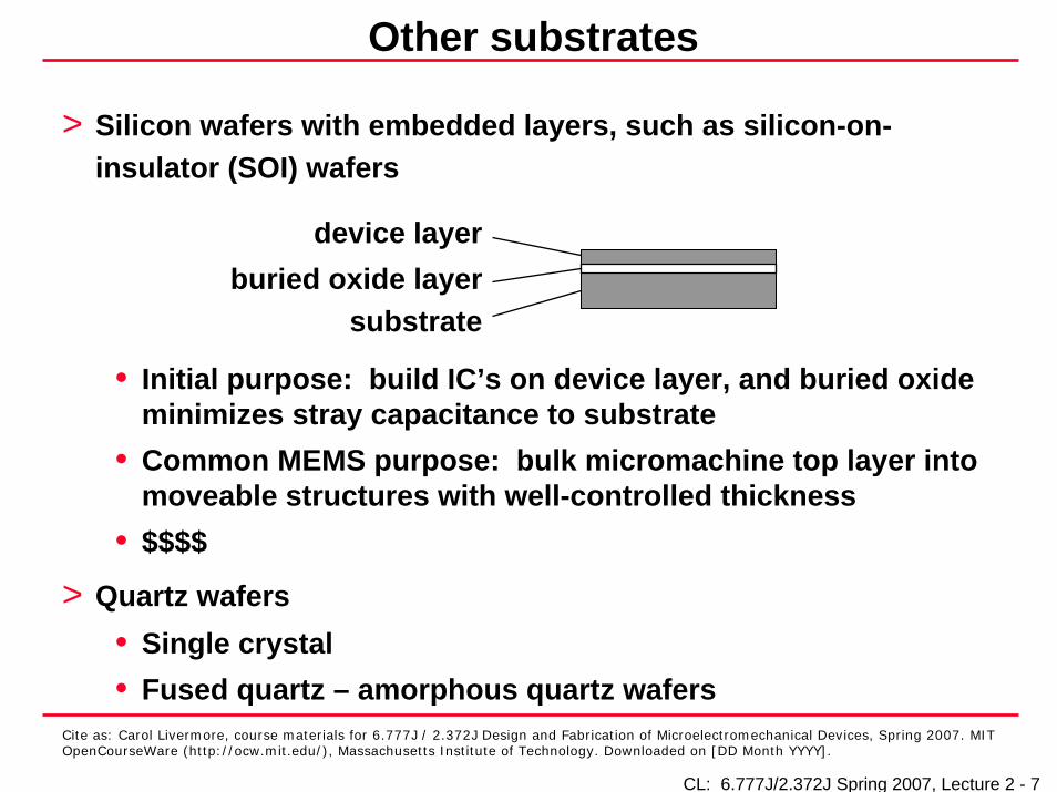
Substrate Front end Back end Everything else compatible compatible compatible
Silicon yes + yes yes, but only use if needed
Silicon on yes + yes yes, but only use insulator (SOI) if needed
Quartz yes yes yes, but only use if needed
Glass (pyrex) no yes, sometimes yes +
Compound no yes yes, but only use semiconductor if needed
Sapphire yes, but only use yes, but only use yes, but only use if needed if needed if needed
CL: 6.777J/2.372J Spring 2007, Lecture 2 - 9
Cite as: Carol Livermore, course materials for 6.777J / 2.372J Design and Fabrication of Microelectromechanical Devices, Spring 2007. MIT OpenCourseWare (http://ocw.mit.edu/), Massachusetts Institute of Technology. Downloaded on [DD Month YYYY].
Substrate summary

CL: 6.777J/2.372J Spring 2007, Lecture 2 - 10
Cite as: Carol Livermore, course materials for 6.777J / 2.372J Design and Fabrication of Microelectromechanical Devices, Spring 2007. MIT OpenCourseWare (http://ocw.mit.edu/), Massachusetts Institute of Technology. Downloaded on [DD Month YYYY].
Outline
> Substrates
> Lithography and patterning
> Doping
> Thin films

CL: 6.777J/2.372J Spring 2007, Lecture 2 - 11
Cite as: Carol Livermore, course materials for 6.777J / 2.372J Design and Fabrication of Microelectromechanical Devices, Spring 2007. MIT OpenCourseWare (http://ocw.mit.edu/), Massachusetts Institute of Technology. Downloaded on [DD Month YYYY].
Optical Lithography
Spin-cast a photosensitive resist layer; bake out solvent
Collimated UV exposure through a mask; resist either cross-links or becomes soluble
Develop by dissolving the exposed/unexposed (positive/negative) resist; can now transfer pattern to substrate
Alignment fiducials permit alignment of subsequent masks.
positive
negative

CL: 6.777J/2.372J Spring 2007, Lecture 2 - 12
larger comfortablyCite as: Carol Livermore, course materials for 6.777J / 2.372J Design and Fabrication of Microelectromechanical Devices, Spring 2007. MIT OpenCourseWare (http://ocw.mit.edu/), Massachusetts Institute of Technology. Downloaded on [DD Month YYYY].
Methods of optical lithography I
> Contact• Mask touches wafer• Inexpensive• Contact degrades mask• No die size limit• Resolution: down to 1 micron nervously; down to several
microns comfortably
> Proximity • Mask of order 10 microns from wafer• Inexpensive• Less mask damage• Diffraction means lower resolution• No die size limit• Resolution: down to several microns nervously, somewhat

Cite as: Carol Livermore, course materials for 6.777J / 2.372J Design and Fabrication of Microelectromechanical Devices, Spring 2007. MIT OpenCourseWare (http://ocw.mit.edu/), Massachusetts Institute of Technology. Downloaded on [DD Month YYYY].
CL: 6.777J/2.372J Spring 2007, Lecture 2 - 13
Projection Lithography> Projection lithography, especially
when combined with an optical imaging system that reduces the image size, is used for high-resolutionpatterning (submicron to very submicron)
> Larger mask features, no contact withmask
> Wafer steppers expose one die at a time, assuring good focus and registration
> Something to consider: if your device needs fine features, a stepper may be required. But steppers have limits on die size of about 1 cm.
Image by MIT OpenCourseWare.Adapted from Figure 3.15 in: Senturia, Stephen D.Microsystem Design. Boston, MA: KluwerAcademic Publishers, 2001, p. 53.ISBN: 9780792372462.
UV Light
CondensingLens
ProjectionOptics
Wafer
Mask

CL: 6.777J/2.372J Spring 2007, Lecture 2 - 14
Cite as: Carol Livermore, course materials for 6.777J / 2.372J Design and Fabrication of Microelectromechanical Devices, Spring 2007. MIT OpenCourseWare (http://ocw.mit.edu/), Massachusetts Institute of Technology. Downloaded on [DD Month YYYY].
Mask making
> Highest quality – chromium on fused quartz written with an electron beam exposing an electron-beam resist (PMMA)
• Also very high quality: laser-writing
> Photographic emulsion on fused quartz exposed with UV light flashes through a programmable aperture
> Patterns printed from an AutoCAD file on transparencies with a very-high-resolution printer – low resolution, but cheap and fast
CL: 6.777J/2.372J Spring 2007, Lecture 2 - 15
Cite as: Carol Livermore, course materials for 6.777J / 2.372J Design and Fabrication of Microelectromechanical Devices, Spring 2007. MIT OpenCourseWare (http://ocw.mit.edu/), Massachusetts Institute of Technology. Downloaded on [DD Month YYYY].
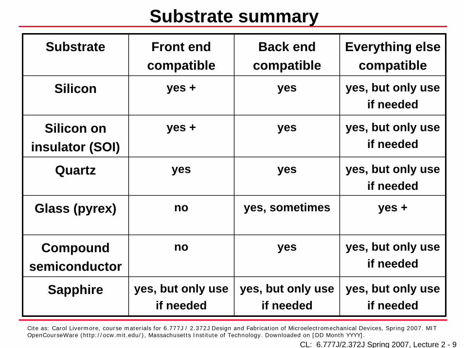
Positive thin resist
> Spin cast
> Thickness of order 1 micron
> Developer removes exposed resist
> Creates sloped profile at resist edge
> Some applications• Wet etching
• Shallow dry etching
> Front end standard

CL: 6.777J/2.372J Spring 2007, Lecture 2 - 16
Cite as: Carol Livermore, course materials for 6.777J / 2.372J Design and Fabrication of Microelectromechanical Devices, Spring 2007. MIT OpenCourseWare (http://ocw.mit.edu/), Massachusetts Institute of Technology. Downloaded on [DD Month YYYY].
Negative/image reversal photoresists
> Spin cast
> Thickness of order 1 micron
> Developer removes unexposed resist
> Creates a re-entrant profile
> Typical application: liftoff processes (in acetone), often seen in back end processing
> Rule of thumb: resist thickness should be 3x thickness of layer to be lifted off
> Not a standard front end material, but not inherently incompatible with it

Cite as: Carol Livermore, course materials for 6.777J / 2.372J Design and Fabrication of Microelectromechanical Devices, Spring 2007. MIT OpenCourseWare (http://ocw.mit.edu/), Massachusetts Institute of Technology. Downloaded on [DD Month YYYY].
CL: 6.777J/2.372J Spring 2007, Lecture 2 - 17
Positive thick photoresist
> Spin cast> Thicknesses of order 10 microns> Sloped profiles
• Slope somewhat controllable through process conditions
> Some planarizing capability> Typical applications:
• Prolonged or low selectivity dry etch
• Deep reactive ion etch• Masking any etch over topography
> Not a standard front end material, but not inherently incompatible with it
5 μm thickCourtesy of Reza Ghodssi. Used with permission.
CL: 6.777J/2.372J Spring 2007, Lecture 2 - 18
Cite as: Carol Livermore, course materials for 6.777J / 2.372J Design and Fabrication of Microelectromechanical Devices, Spring 2007. MIT OpenCourseWare (http://ocw.mit.edu/), Massachusetts Institute of Technology. Downloaded on [DD Month YYYY].
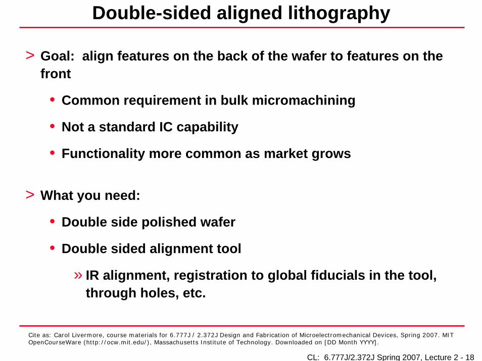
Double-sided aligned lithography
> Goal: align features on the back of the wafer to features on the front
• Common requirement in bulk micromachining
• Not a standard IC capability
• Functionality more common as market grows
> What you need:
• Double side polished wafer
• Double sided alignment tool
» IR alignment, registration to global fiducials in the tool, through holes, etc.

CL: 6.777J/2.372J Spring 2007, Lecture 2 - 19
Cite as: Carol Livermore, course materials for 6.777J / 2.372J Design and Fabrication of Microelectromechanical Devices, Spring 2007. MIT OpenCourseWare (http://ocw.mit.edu/), Massachusetts Institute of Technology. Downloaded on [DD Month YYYY].
Special purpose lithographic techniques I> X-ray lithography
• One application: making molds for LIGA• Requires an x-ray source and x-ray mask
> Electron beam lithography• High resolution (tens of nanometers)• NEMS (NanoElectroMechanical Systems)• A slow, serial process
> Lithographic techniques that are rarely seen in front end processing

CL: 6.777J/2.372J Spring 2007, Lecture 2 - 20
Cite as: Carol Livermore, course materials for 6.777J / 2.372J Design and Fabrication of Microelectromechanical Devices, Spring 2007. MIT OpenCourseWare (http://ocw.mit.edu/), Massachusetts Institute of Technology. Downloaded on [DD Month YYYY].
Special purpose lithographic techniques II> Shadow masking
• Direct evaporation or sputtering through physical holes in a shadow mask (think stencils)
• Back end/everything else process• “Last ditch” technique for patterning surfaces that cannot be
coated with resist (large topography, fragile features)
> “Soft lithography” (Whitesides, Harvard)• Using polydimethylsiloxane (PDMS, a rubber material) as a
physical mold to replicate structures• Advantages:
» Patterning curved surfaces» Rapid, inexpensive fabrication
• A set of everything else processes• More on this later

CL: 6.777J/2.372J Spring 2007, Lecture 2 - 21
Cite as: Carol Livermore, course materials for 6.777J / 2.372J Design and Fabrication of Microelectromechanical Devices, Spring 2007. MIT OpenCourseWare (http://ocw.mit.edu/), Massachusetts Institute of Technology. Downloaded on [DD Month YYYY].
Very thick photoresists
> SU-8 epoxy• Spin cast• Negative resist, optical
exposure• Can planarize extreme
topographies• Can be structural, not easily
dissolved
> Polyimide• Spin cast• Can planarize topographies• Humidity sensitive
> Classified as “everything else”
Image removed due to copyright restrictions.
Image removed due to copyright restrictions.
SU-8 epoxy photograph.
500 micrometer SU-8 epoxy within deep silicon trench.
CL: 6.777J/2.372J Spring 2007, Lecture 2 - 22
Cite as: Carol Livermore, course materials for 6.777J / 2.372J Design and Fabrication of Microelectromechanical Devices, Spring 2007. MIT OpenCourseWare (http://ocw.mit.edu/), Massachusetts Institute of Technology. Downloaded on [DD Month YYYY].
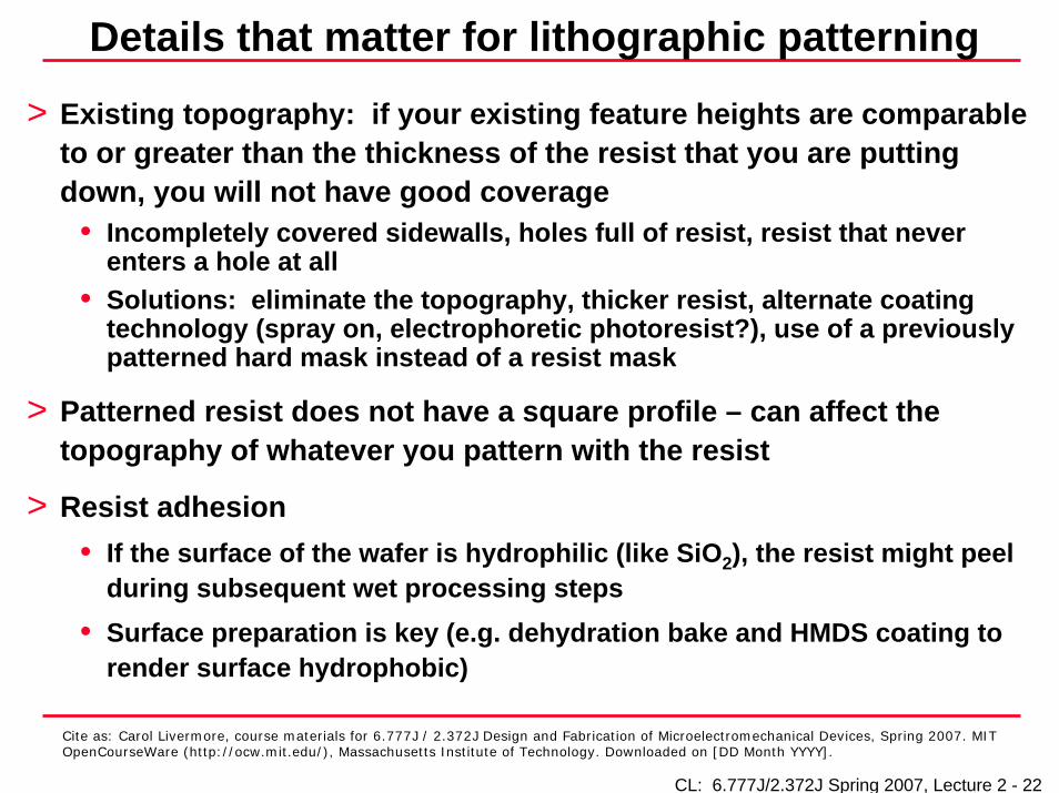
Details that matter for lithographic patterning
> Existing topography: if your existing feature heights are comparable to or greater than the thickness of the resist that you are putting down, you will not have good coverage
• Incompletely covered sidewalls, holes full of resist, resist that never enters a hole at all
• Solutions: eliminate the topography, thicker resist, alternate coating technology (spray on, electrophoretic photoresist?), use of a previously patterned hard mask instead of a resist mask
> Patterned resist does not have a square profile – can affect the topography of whatever you pattern with the resist
> Resist adhesion• If the surface of the wafer is hydrophilic (like SiO2), the resist might peel
during subsequent wet processing steps• Surface preparation is key (e.g. dehydration bake and HMDS coating to
render surface hydrophobic)

CL: 6.777J/2.372J Spring 2007, Lecture 2 - 23
Cite as: Carol Livermore, course materials for 6.777J / 2.372J Design and Fabrication of Microelectromechanical Devices, Spring 2007. MIT OpenCourseWare (http://ocw.mit.edu/), Massachusetts Institute of Technology. Downloaded on [DD Month YYYY].
Cleaning!
> When we say (for example) that positive thin resist is compatible with front end processing, we do not mean that you can have resist onyour wafer during most front end processes!
> Must remove resist and clean wafer thoroughly before high temperature processes
> Always include cleaning in process flows, starting at the crayonengineering level
> Resist removal techniques:• O2 plasma ash• Chemical removal of organics: piranha clean (3:1 H2SO4:H202) or
Nanostrip (a weaker version of piranha)• Solvents (acetone)

CL: 6.777J/2.372J Spring 2007, Lecture 2 - 24
Cite as: Carol Livermore, course materials for 6.777J / 2.372J Design and Fabrication of Microelectromechanical Devices, Spring 2007. MIT OpenCourseWare (http://ocw.mit.edu/), Massachusetts Institute of Technology. Downloaded on [DD Month YYYY].
More cleaning!> Additional cleans typically needed at specified points in the flow
> Example: RCA clean before very high temperature processing (as in furnace for front end processing)
• Step 1: Organic clean, 5:1:1 H2O:H2O2:NH4OH at 75 - 80C• Step 2: Thin oxide removal, 50:1 H2 O:HF • Step 3: Metal/ionic contamination removal, 6:1:1 H2O:H2O2: HCl at 75 –
80C
> Example: remove organics before moderately high temperature, fairly clean processing (upper part of back end processing)
• Piranha clean (3:1 H2SO4:H202)
> Materials compatibility (what cleans your structures can tolerate) often determine what processes you can and can’t use
> If you wait until the last minute to put cleans into your process flow, you will likely be redesigning your device and process at the last minute

CL: 6.777J/2.372J Spring 2007, Lecture 2 - 25
Cite as: Carol Livermore, course materials for 6.777J / 2.372J Design and Fabrication of Microelectromechanical Devices, Spring 2007. MIT OpenCourseWare (http://ocw.mit.edu/), Massachusetts Institute of Technology. Downloaded on [DD Month YYYY].
Another important detail: process bias
> The feature drawn on the mask is not the same size as the feature produced on the wafer
> Exposed area usually extends beyond clear area on mask
> Resist selection impacts process bias• Resist thickness• Resist tone

CL: 6.777J/2.372J Spring 2007, Lecture 2 - 26
Cite as: Carol Livermore, course materials for 6.777J / 2.372J Design and Fabrication of Microelectromechanical Devices, Spring 2007. MIT OpenCourseWare (http://ocw.mit.edu/), Massachusetts Institute of Technology. Downloaded on [DD Month YYYY].
Design Rules
> Alignment of one pattern to the next is critical to device fabrication
> Design rules are created to assure that fabrication tolerances do not destroy devices
Image by MIT OpenCourseWare.Adapted from Figure 3.16 in: Senturia, Stephen D. Microsystem Design.Norwell, MA: Kluwer Academic Publishers, 2001, p. 54. ISBN: 9780792372462.
Barely acceptable misalignment
After Mask 1
Unacceptable misalignment
Desired alignmentFeature onMask 2
Feature onMask 1
MandatoryOverlapDesign Rule
After Mask 2:

CL: 6.777J/2.372J Spring 2007, Lecture 2 - 27
Cite as: Carol Livermore, course materials for 6.777J / 2.372J Design and Fabrication of Microelectromechanical Devices, Spring 2007. MIT OpenCourseWare (http://ocw.mit.edu/), Massachusetts Institute of Technology. Downloaded on [DD Month YYYY].
Outline
> Substrates
> Lithography and patterning
> Doping
> Thin films

CL: 6.777J/2.372J Spring 2007, Lecture 2 - 28
Cite as: Carol Livermore, course materials for 6.777J / 2.372J Design and Fabrication of Microelectromechanical Devices, Spring 2007. MIT OpenCourseWare (http://ocw.mit.edu/), Massachusetts Institute of Technology. Downloaded on [DD Month YYYY].
Doping
> Doping is the introduction of a controlled amount of impurities to change the conductivity type and degree of a semiconductor
> In silicon, boron is a p-type dopant (creating holes), while phosphorus, arsenic, and antimony are n-type dopants(creating conduction electrons)
> Some doping incorporated in initial silicon melt
> All modern thin film doping is done with ion implanation
> Doping doesn’t add a new thin film, but it modifies the properties of a thin film at the surface of existing material

CL: 6.777J/2.372J Spring 2007, Lecture 2 - 29
Cite as: Carol Livermore, course materials for 6.777J / 2.372J Design and Fabrication of Microelectromechanical Devices, Spring 2007. MIT OpenCourseWare (http://ocw.mit.edu/), Massachusetts Institute of Technology. Downloaded on [DD Month YYYY].
Ion implantation
> A high-voltage accelerator is used to shoot ions at the wafer.
> The beam must be rastered and the wafer must be rotated to achieve uniform dose
> Usually a thin protective layer, such as oxide, is used to prevent sputtering of the surface and to reduce channeling
> The depth of the implant dose depends on energy
> Activation anneal after implantation allows dopants to reach proper positions in crystal

CL: 6.777J/2.372J Spring 2007, Lecture 2 - 30
Cite as: Carol Livermore, course materials for 6.777J / 2.372J Design and Fabrication of Microelectromechanical Devices, Spring 2007. MIT OpenCourseWare (http://ocw.mit.edu/), Massachusetts Institute of Technology. Downloaded on [DD Month YYYY].
Effective range> The effective range measures the location of the
peak concentration of an implanted species.
100010010Energy (keV)
0.001
0.01
0.1
1
10
Proj
ecte
d ra
nge
(m)
Arsenic
Phosphorus
Boron
This image is for illustration purposes only; it should not be used for design calculations.Adapted from Figure 3.6 in Senturia, Stephen D. Microsystem Design. Boston, MA:Kluwer Academic Publishers, 2001, p. 39. ISBN: 9780792372462.
Image by MIT OpenCourseWare.
CL: 6.777J/2.372J Spring 2007, Lecture 2 - 31
Cite as: Carol Livermore, course materials for 6.777J / 2.372J Design and Fabrication of Microelectromechanical Devices, Spring 2007. MIT OpenCourseWare (http://ocw.mit.edu/), Massachusetts Institute of Technology. Downloaded on [DD Month YYYY].
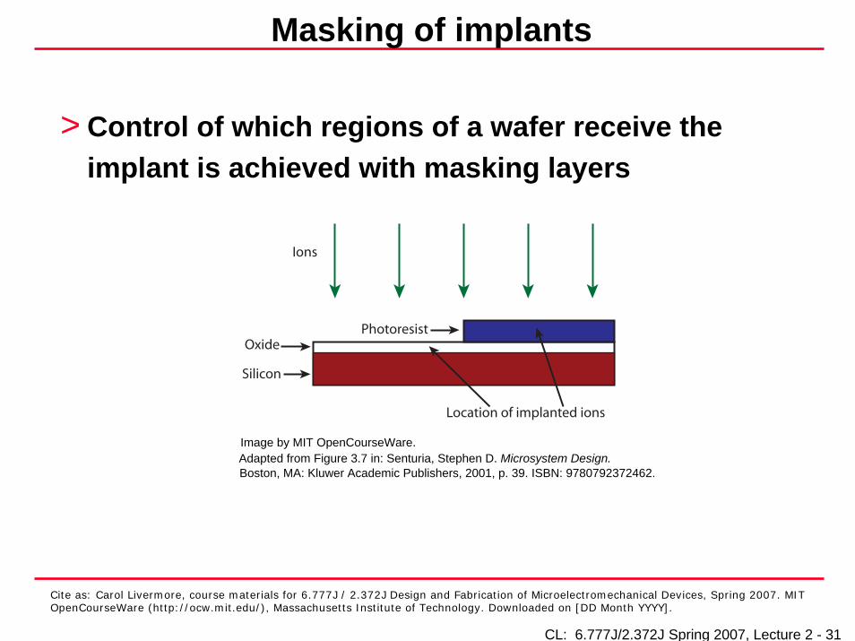
Masking of implants
> Control of which regions of a wafer receive the implant is achieved with masking layers
Image by MIT OpenCourseWare.Adapted from Figure 3.7 in: Senturia, Stephen D. Microsystem Design.Boston, MA: Kluwer Academic Publishers, 2001, p. 39. ISBN: 9780792372462.
Ions
Photoresist
Silicon
Location of implanted ions
Oxide
CL: 6.777J/2.372J Spring 2007, Lecture 2 - 32
Cite as: Carol Livermore, course materials for 6.777J / 2.372J Design and Fabrication of Microelectromechanical Devices, Spring 2007. MIT OpenCourseWare (http://ocw.mit.edu/), Massachusetts Institute of Technology. Downloaded on [DD Month YYYY].
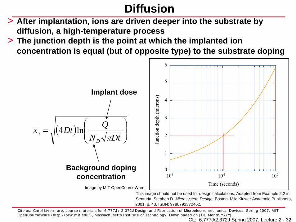
Diffusion> After implantation, ions are driven deeper into the substrate by
diffusion, a high-temperature process> The junction depth is the point at which the implanted ion
concentration is equal (but of opposite type) to the substrate doping
( ) ⎟⎟⎠
⎞⎜⎜⎝
⎛=
DtNQDtx
Dj π
ln4
Implant dose
Background doping concentration
5
6
4
3
2
1
0103 104 105
Junc
tion
dept
h (m
icro
ns)
Time (seconds)
This image should not be used for design calculations. Adapted from Example 2.2 in:Senturia, Stephen D. Microsystem Design. Boston, MA: Kluwer Academic Publishers,2001, p. 43. ISBN: 9780792372462.
Image by MIT OpenCourseWare.

CL: 6.777J/2.372J Spring 2007, Lecture 2 - 33
Cite as: Carol Livermore, course materials for 6.777J / 2.372J Design and Fabrication of Microelectromechanical Devices, Spring 2007. MIT OpenCourseWare (http://ocw.mit.edu/), Massachusetts Institute of Technology. Downloaded on [DD Month YYYY].
Outline
> Substrates
> Lithography and patterning
> Doping
> Thin films

CL: 6.777J/2.372J Spring 2007, Lecture 2 - 34
Cite as: Carol Livermore, course materials for 6.777J / 2.372J Design and Fabrication of Microelectromechanical Devices, Spring 2007. MIT OpenCourseWare (http://ocw.mit.edu/), Massachusetts Institute of Technology. Downloaded on [DD Month YYYY].
Creating thin (and thick) films> Many techniques to choose from> Differences:
• Front or back end processes• Quality of resulting films (electrical properties, etch
selectivity, defects, residual stress)• Conformality• Deposition rate, cost
> Physical techniques• Material is removed from a source, carried to the substrate,
and dropped there> Chemical techniques
• Reactants are transported to the substrate, a chemical reaction occurs, and the products deposit on the substrate to form the desired film

CL: 6.777J/2.372J Spring 2007, Lecture 2 - 35
Cite as: Carol Livermore, course materials for 6.777J / 2.372J Design and Fabrication of Microelectromechanical Devices, Spring 2007. MIT OpenCourseWare (http://ocw.mit.edu/), Massachusetts Institute of Technology. Downloaded on [DD Month YYYY].
Taxonomy of deposition techniques> Chemical
• Thermal Oxidation • Chemical Vapor Deposition (CVD)
» Low Pressure (LPCVD), Atmospheric Pressure (APCVD), Plasma Enhanced (PECVD)
• Epitaxy• Electrodeposition (Electroplating)
> Physical• Physical Vapor Deposition (PVD)
» Evaporation» Sputtering
• Spin-casting

CL: 6.777J/2.372J Spring 2007, Lecture 2 - 36
Cite as: Carol Livermore, course materials for 6.777J / 2.372J Design and Fabrication of Microelectromechanical Devices, Spring 2007. MIT OpenCourseWare (http://ocw.mit.edu/), Massachusetts Institute of Technology. Downloaded on [DD Month YYYY].
Oxidation I
> Silicon forms a high quality, stable oxide> How it works:
• Oxygen diffuses through oxide to Si/oxide interface• Si + O2 + high temperature (~1100 C) furnace SiO2
• Some Si is consumed
> Rate determined by diffusion of oxygen through oxide> Diffusion limits practical oxide thickness to < 2 μm> A key front end process
0.46 toxtox

CL: 6.777J/2.372J Spring 2007, Lecture 2 - 37
Cite as: Carol Livermore, course materials for 6.777J / 2.372J Design and Fabrication of Microelectromechanical Devices, Spring 2007. MIT OpenCourseWare (http://ocw.mit.edu/), Massachusetts Institute of Technology. Downloaded on [DD Month YYYY].
Oxidation II
> Dry oxidation (O2)• High quality, slow oxidation rate, smaller maximum thickness
(i.e. gate oxide)
> Wet oxidation (steam)• H2 to speed the diffusion• Lower quality, faster oxidation rate
> The Deal-Grove model describes the kinetics of oxidation quite well for oxides greater in thickness than about 30 nm.

CL: 6.777J/2.372J Spring 2007, Lecture 2 - 38
Cite as: Carol Livermore, course materials for 6.777J / 2.372J Design and Fabrication of Microelectromechanical Devices, Spring 2007. MIT OpenCourseWare (http://ocw.mit.edu/), Massachusetts Institute of Technology. Downloaded on [DD Month YYYY].
Deal-Grove Model
( )⎥⎥
⎦
⎤
⎢⎢
⎣
⎡
⎥⎥⎦
⎤
⎢⎢⎣
⎡−++= 1
415.0 2 τ DG
DG
DGDGfinal t
ABAx
ABx
Bx
DGDG
i
DG
iDG /
2
+=τ
For oxides greater than about 30 nm thick:
where
(Constants are given in the text; beware units of BDG, μm2/hour)
Growth goes approximately as t for short times, and approximately as for long times.t

CL: 6.777J/2.372J Spring 2007, Lecture 2 - 39
Cite as: Carol Livermore, course materials for 6.777J / 2.372J Design and Fabrication of Microelectromechanical Devices, Spring 2007. MIT OpenCourseWare (http://ocw.mit.edu/), Massachusetts Institute of Technology. Downloaded on [DD Month YYYY].
Local Oxidation
> Oxidation can be masked locally by an oxidation barrier, such assilicon nitride
> Oxide undercuts edge of mask layer to form a “bird’s beak”
> Oxidation followed by oxide etch can also be used to sharpen silicon features.
Senturia, Microsystem Design.Image by MIT OpenCourseWare.Adapted from Figure 3.5 in: Senturia, Stephen D. Microsystem Design.Norwell, MA: Kluwer Academic Publishers, 2001, p. 37. ISBN: 9780792372462.
Silicon wafer
Bird’s beaks
After oxidation
Oxidation barrier

Cite as: Carol Livermore, course materials for 6.777J / 2.372J Design and Fabrication of Microelectromechanical Devices, Spring 2007. MIT OpenCourseWare (http://ocw.mit.edu/), Massachusetts Institute of Technology. Downloaded on [DD Month YYYY].
CL: 6.777J/2.372J Spring 2007, Lecture 2 - 40
Chemical Vapor Deposition (CVD)> How CVD works:
• Gaseous reactants, often at low pressure• Long mean free path; reactants reach substrate• Reactants react and deposit products on the substrate• Unlike oxidation, does not consume substrate material
> Energy sources facilitate CVD reactions:• High temperature, plasma, laser
> Processing temperatures vary widely
> Commonly deposited films: Oxide, silicon nitride, polysilicon
> CVD results depend on pressures, gas flows, temperature• Film composition, uniformity, deposition rate, and electrical and
mechanical characteristics can vary> Near the boundary between front and back end, depending

CL: 6.777J/2.372J Spring 2007, Lecture 2 - 41
Cite as: Carol Livermore, course materials for 6.777J / 2.372J Design and Fabrication of Microelectromechanical Devices, Spring 2007. MIT OpenCourseWare (http://ocw.mit.edu/), Massachusetts Institute of Technology. Downloaded on [DD Month YYYY].
Some reasons to use CVD
> Oxide formation:• To get a thicker layer than thermal oxidation can provide• To create oxide on a wafer that can’t withstand high
temperatures (for example because of metal features)• To create oxide on top of a material that is not silicon
> For film formation in general:• To tailor the film properties (like film stress) by adjusting
pressures, flow rates, external energy supply, ratios of different precursor gases (to adjust proportions of different materials inthe final product)
• Conformality: (more or less) even coating on all surfaces
> Drawbacks• Films deposited at low temperature are often lower quality than
high temperature versions, and have less predictable properties• Flammable, toxic, or corrosive source gases

CL: 6.777J/2.372J Spring 2007, Lecture 2 - 42
Cite as: Carol Livermore, course materials for 6.777J / 2.372J Design and Fabrication of Microelectromechanical Devices, Spring 2007. MIT OpenCourseWare (http://ocw.mit.edu/), Massachusetts Institute of Technology. Downloaded on [DD Month YYYY].
Thick Film Formation> Chemical vapor deposition is a common MEMS tool for creating thick
films on the wafer surface• In practice, film stress limits thickness (film delamination or cracking, or
curvature of underlying structures)• Can deposit thick oxides; nitrides are still typically submicron• Must anneal deposited oxides for some applications – lose low stress
property on anneal
> Example: PECVD deposition (350-400C) of 10 to 20 μm oxides
18 μm thick oxide insulation for a microgenerator w/ Pt features
25 μm thick cracked oxide, X. Zhang et al., Hilton Head 2000
Image removed due to copyright restrictions. Image removed due to copyright restrictions.

CL: 6.777J/2.372J Spring 2007, Lecture 2 - 43
Figure 5 on p. 606 in: Arana, L.R., S. B. Schaevitz, A. J. Franz,Figure 4 on p. 605 in: Arana, L.R., S. B. Schaevitz, A. J. Franz,M. A. Schmidt, K. F. Jensen, "A Microfabricated Suspended-tubeM. A. Schmidt, K. F. Jensen, "A Microfabricated Suspended-tubeChemical Reactor for Thermally Efficient Fuel Processing." JournalChemical Reactor for Thermally Efficient Fuel Processing." Journalof Microelectromechanical Systems 12, no. 5 (2003): 600-612. ©of Microelectromechanical Systems 12, no. 5 (2003): 600-612. ©2003 IEEE.2003 IEEE.
Cite as: Carol Livermore, course materials for 6.777J / 2.372J Design and Fabrication of Microelectromechanical Devices, Spring 2007. MIT OpenCourseWare (http://ocw.mit.edu/), Massachusetts Institute of Technology. Downloaded on [DD Month YYYY].
CVD enables conformal coating
MEMS-based fuel processor.

CL: 6.777J/2.372J Spring 2007, Lecture 2 - 44
Cite as: Carol Livermore, course materials for 6.777J / 2.372J Design and Fabrication of Microelectromechanical Devices, Spring 2007. MIT OpenCourseWare (http://ocw.mit.edu/), Massachusetts Institute of Technology. Downloaded on [DD Month YYYY].
LPCVD Polysilicon> Amorphous at lower deposition temperatures and higher
deposition rates• Typical temperature: ~ 590 C
> Polycrystalline at higher deposition temperatures and lower deposition rates • Typical temperature: ~ 625 C
> Grain size and structure depend on detailed deposition conditions• e.g. thicker films ⇒ larger grains
> Structure, electrical properties, and mechanical properties alsovary with post-deposition thermal processing • Grain growth• Dopant activation or diffusion

CL: 6.777J/2.372J Spring 2007, Lecture 2 - 45
Cite as: Carol Livermore, course materials for 6.777J / 2.372J Design and Fabrication of Microelectromechanical Devices, Spring 2007. MIT OpenCourseWare (http://ocw.mit.edu/), Massachusetts Institute of Technology. Downloaded on [DD Month YYYY].
Polysilicon stress depends on deposition details
Kurt Petersen, Trans Sensory Devices
Image removed due to copyright restrictions.Image removed due to copyright restrictions.
Lober, Theresa Ann. "A Microfabricated ElectrostaticMotor Design and Process." Masters thesis, MassachusettsInstitute of Technology, 1988. 132 pages.
Image removed due to copyright restrictions.

CL: 6.777J/2.372J Spring 2007, Lecture 2 - 46
Cite as: Carol Livermore, course materials for 6.777J / 2.372J Design and Fabrication of Microelectromechanical Devices, Spring 2007. MIT OpenCourseWare (http://ocw.mit.edu/), Massachusetts Institute of Technology. Downloaded on [DD Month YYYY].
Epitaxy
> CVD deposition process in which atoms move to lattice sites, continuing the substrate’s crystal structure
• Homoepitaxy: same material, i.e. Si on Si• Heteroepitaxy: different materials, i.e. AlGaAs on GaAs
> How it happens
• Slow deposition rate (enough time to find a lattice site)• High temperature (enough energy to move to a lattice site)
> Selective epitaxy is possible through masking
> Can grow a doped Si layer of known thickness

CL: 6.777J/2.372J Spring 2007, Lecture 2 - 47
Cite as: Carol Livermore, course materials for 6.777J / 2.372J Design and Fabrication of Microelectromechanical Devices, Spring 2007. MIT OpenCourseWare (http://ocw.mit.edu/), Massachusetts Institute of Technology. Downloaded on [DD Month YYYY].
Electroplating: basics
> Pass a current through an aqueous metal solution• Anode is made of the metal that you want to deposit• Cathode is the conductive seed material on your wafer• Positive metal ions travel to the negatively charged cathode on
your wafer and deposit there
> Preparing your wafer• If you want to plate metal in some places and not in others, you will
need a patterned metal seed layer (and typically a “sticky” metal adhesion layer under that)
• For very short features, just plate onto the seed layer• For taller features, need to plate into a mold• Molds can be photoresist, silicon, SU-8, etc., depending on the
needs of your device
CL: 6.777J/2.372J Spring 2007, Lecture 2 - 48
Cite as: Carol Livermore, course materials for 6.777J / 2.372J Design and Fabrication of Microelectromechanical Devices, Spring 2007. MIT OpenCourseWare (http://ocw.mit.edu/), Massachusetts Institute of Technology. Downloaded on [DD Month YYYY].
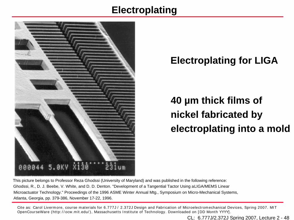
Electroplating
Electroplating for LIGA
40 µm thick films of nickel fabricated by electroplating into a mold
This picture belongs to Professor Reza Ghodssi (University of Maryland) and was published in the following reference:Ghodssi, R., D. J. Beebe, V. White, and D. D. Denton. "Development of a Tangential Tactor Using a LIGA/MEMS LinearMicroactuator Technology." Proceedings of the 1996 ASME Winter Annual Mtg., Symposium on Micro-Mechanical Systems,Atlanta, Georgia, pp. 379-386, November 17-22, 1996.

CL: 6.777J/2.372J Spring 2007, Lecture 2 - 49
Cite as: Carol Livermore, course materials for 6.777J / 2.372J Design and Fabrication of Microelectromechanical Devices, Spring 2007. MIT OpenCourseWare (http://ocw.mit.edu/), Massachusetts Institute of Technology. Downloaded on [DD Month YYYY].
Electroplating realities
Test run w/ bump plating - perfect
Real device forms keyholes – different loading pattern
Solution: Cu damascene fill, with additives/agitation to promote fill at bottom
Courtesy of Dariusz Golda. Used with permission.

CL: 6.777J/2.372J Spring 2007, Lecture 2 - 50
Cite as: Carol Livermore, course materials for 6.777J / 2.372J Design and Fabrication of Microelectromechanical Devices, Spring 2007. MIT OpenCourseWare (http://ocw.mit.edu/), Massachusetts Institute of Technology. Downloaded on [DD Month YYYY].
Conformality and keyholes
> To lowest order, conformal films coat sidewalls and horizontal surfaces at the same rate.
> But high aspect ratio trenches are prone to keyholes (CVD, electroplating, etc.)
What you want: What you get:
CL: 6.777J/2.372J Spring 2007, Lecture 2 - 51
Cite as: Carol Livermore, course materials for 6.777J / 2.372J Design and Fabrication of Microelectromechanical Devices, Spring 2007. MIT OpenCourseWare (http://ocw.mit.edu/), Massachusetts Institute of Technology. Downloaded on [DD Month YYYY].
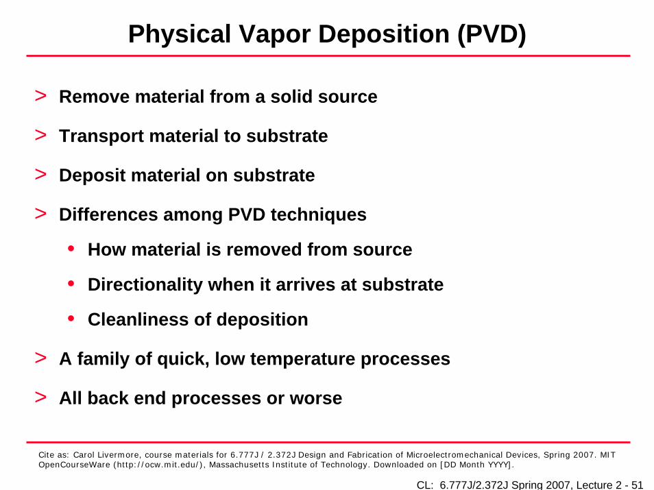
Physical Vapor Deposition (PVD)
> Remove material from a solid source
> Transport material to substrate
> Deposit material on substrate
> Differences among PVD techniques
• How material is removed from source
• Directionality when it arrives at substrate
• Cleanliness of deposition
> A family of quick, low temperature processes
> All back end processes or worse

CL: 6.777J/2.372J Spring 2007, Lecture 2 - 52
Cite as: Carol Livermore, course materials for 6.777J / 2.372J Design and Fabrication of Microelectromechanical Devices, Spring 2007. MIT OpenCourseWare (http://ocw.mit.edu/), Massachusetts Institute of Technology. Downloaded on [DD Month YYYY].
Thermal Evaporation
> Source is resistively heated in high vacuum• Typical source: metal
> Hot source atoms are emitted in all directions and stick where they land
> Substrate receives a directional flux of source material• Good for liftoff processes, otherwise poor conformality
> Possible contamination from generalized heating
I Rsource

CL: 6.777J/2.372J Spring 2007, Lecture 2 - 53
Cite as: Carol Livermore, course materials for 6.777J / 2.372J Design and Fabrication of Microelectromechanical Devices, Spring 2007. MIT OpenCourseWare (http://ocw.mit.edu/), Massachusetts Institute of Technology. Downloaded on [DD Month YYYY].
E-beam Evaporation
> Electron beam heats source in high vacuum• Typical source: metal
> Hot source atoms are emitted in all directions and stick where they land
> Substrate receives a directional flux of source material• Good for liftoff processes, otherwise poor conformality
> Heating is less generalized less contamination
V
source
electrongun
e-
CL: 6.777J/2.372J Spring 2007, Lecture 2 - 54
Cite as: Carol Livermore, course materials for 6.777J / 2.372J Design and Fabrication of Microelectromechanical Devices, Spring 2007. MIT OpenCourseWare (http://ocw.mit.edu/), Massachusetts Institute of Technology. Downloaded on [DD Month YYYY].
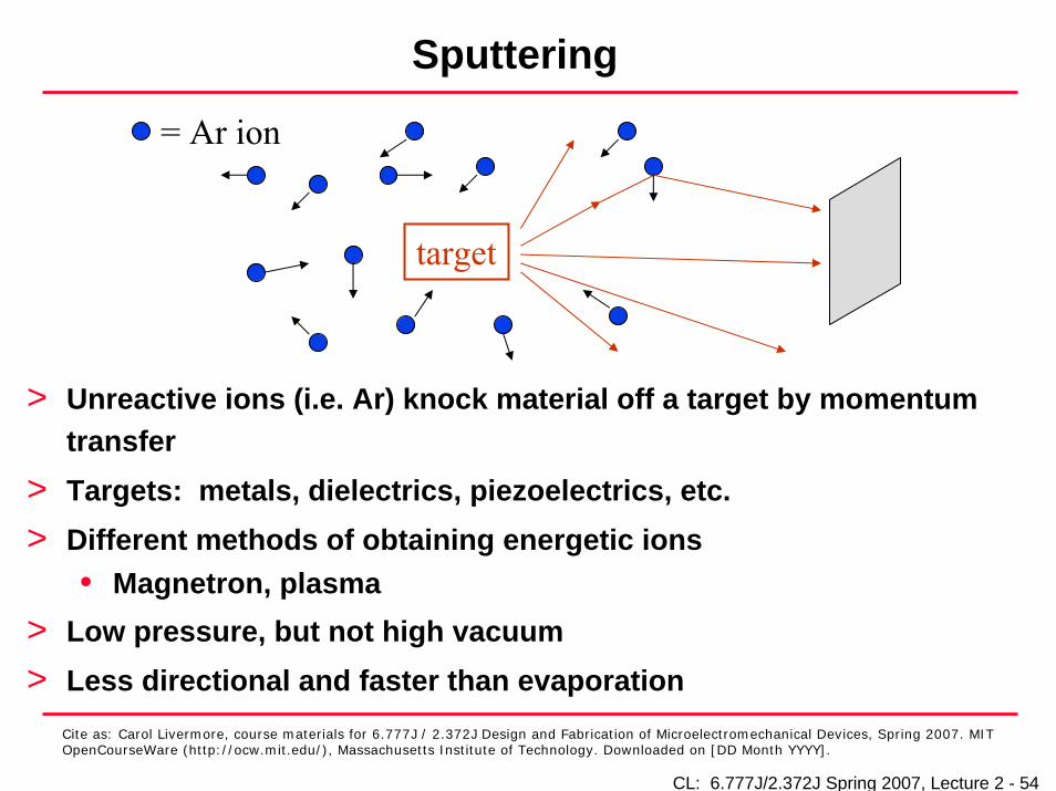
Sputtering
> Unreactive ions (i.e. Ar) knock material off a target by momentum transfer
> Targets: metals, dielectrics, piezoelectrics, etc.> Different methods of obtaining energetic ions
• Magnetron, plasma> Low pressure, but not high vacuum > Less directional and faster than evaporation
target
= Ar ion

CL: 6.777J/2.372J Spring 2007, Lecture 2 - 55
Cite as: Carol Livermore, course materials for 6.777J / 2.372J Design and Fabrication of Microelectromechanical Devices, Spring 2007. MIT OpenCourseWare (http://ocw.mit.edu/), Massachusetts Institute of Technology. Downloaded on [DD Month YYYY].
Etching, liftoff, and adhesion layers
> Films are patterned differently depending on whether the material in question tends to react with other materials
> Materials that react (for example, aluminum):• Deposit a blanket film (sputtering good for better conformality), do
photolithography, and etch it into the desired shape
> Materials that don’t react readily (for example, noble metals):• Hard to etch: typically use liftoff instead• Pattern resist, then deposit metal on top with a directional deposition tool• Not very sticky: typically need an adhesion layer to stick the noble metal
to what lies beneath• Example: use a few hundred A thick layer of Cr or Ti to adhere Au to an
underlying oxide (deposited without breaking vacuum between layers)

CL: 6.777J/2.372J Spring 2007, Lecture 2 - 56
Cite as: Carol Livermore, course materials for 6.777J / 2.372J Design and Fabrication of Microelectromechanical Devices, Spring 2007. MIT OpenCourseWare (http://ocw.mit.edu/), Massachusetts Institute of Technology. Downloaded on [DD Month YYYY].
Is this all you can do with deposited films?> No!
> Spin-casting: put the stuff that you want to deposit in a liquid, spin it onto the surface like resist, and bake out the solvent (spin on glass, PZT piezoelectrics)
> Other forms of vapor deposition designed for a particular purpose (depositing the inert polymer parylene by vapor deposition followed by polymerization)
> Lamination of free-standing resist films onto surfaces
> Self assembled monolayers
> …


![Dissipation and The Thermal Energy Domain Part I...Downloaded on [DD Month YYYY]. J. Voldman: 2.372J/6.777J Spring 2007, Lecture 12 - 2 Outline >Thermal energy domain: why we love](https://img.pdfslide.net/doc/110x75/5ecbb057e0ff6f138423c67b/dissipation-and-the-thermal-energy-domain-part-i-downloaded-on-dd-month-yyyy.jpg)