Embed Size (px)
Citation preview

MICROFLUIDICS AND ENABLING TECHNOLOGY
LAB MODULE 1 Fabrication of PDMS-based Microfluidics
Location 3300 Micro and Nanotechnology Laboratory (MNTL) Instructors Angana Senpan Micro and Nanotechnology Laboratory BioLab Manager and Jiwook Shim Electrical and Computer Engineering Purpose and Expected Outcome
The purpose of this laboratory module is to provide an introduction and hands-on demonstrations of both the micro-fabrication of PDMS devices and the methods of controlling fluid flow within the device We will start with a SU-8 master and fabricate devices in PDMS assemble the chip and modulate flow while monitoring polystyrene beads andor food dyes within the device Overview of Polydimethyl Siloxane (PDMS) Device Fabrication
PDMS device fabrication is one of the easiest methods for the rapid prototyping of microfluidic devices The main steps in the fabrication process are sketched in Scheme 1 below
Scheme 1 Schematic overview of PDMS Device Fabrication In this experimental module we will perform the steps outlined above in yellow The general principles of microfabrication are important considerations for the production of ideal masters This includes the design and manufacture of positive resists and matching resists to the proper reticles or transparencies The bonding of the elastomer device will be discussed a process that is accomplished with an UV-ozone source Post-bonding surface modifications of PDMS are additional surface chemistry alterations that
Bonding Surface (glass PDMS etc)
PDMS replica
Silicon Wafer
SU-8 Features PDMS
Pour PDMS prepolymer
and cure (65 ordmC 2 hours)
Peel PDMS replica from master cut out device
punch tubing inlets
Bond PDMS to glass slides A) Conformal contact or B) Expose to O2 plasma (100 mW RF 1 oxygen 30 sec)
Design and fabricate
SU-8 Master
Microfluidics Page 2 of 5
enable the functionalization of PDMS and channels Such surface modifications are advantageous for functionizing microchannels for studies investigating the interaction of cells and microdomains PDMS is a flexible elastomeric polymer that is an excellent material for microfluidic device fabrication1 In this lab module we will use one of the most common PDMS elastomers Sylgardreg 184 from Dow Corningreg Sylgard is a two part resin system containing vinyl groups (part A) and hydrosiloxane groups (part B) shown in Scheme 2 below Mixing the two resin components together leads to a cross-linked network of dimethyl siloxane groups Because this material is flexible it can be unmolded (peeled) from the SU-8 master leaving the master intact and ready to produce another device
O
Si
H
CH3
O
H2C
HC
Si
O
CH3
CH3
+ Catalyst O
Si
CH3
O
Si
O
CH3
CH3
Part BPart A
Scheme 2 PDMS Crosslinking Once the device is peeled from the mold it is prepared for assembly into a final device Devices are cut to size with standard surgical steel blades and access holes are punched to the desired size for tubing or fluidic reservoirs For tubing inputs a needle hole is drilled slightly smaller than the outer diameter of the tubing being used This provides adequate sealing for typical fluidic pressures For fluidic reservoirs for use without micropumps wells can be punched (using dermal biopsy punches) into the PDMS to sustain fluidic flow depending on the required duration of the selected application Another useful property of PDMS is that its surface can be chemically modified in order to obtain the interfacial properties of interest2 The most reliable method to covalently functionalize PDMS is to expose it to an oxygen plasma whereby surface Si-CH3 groups along the PDMS backbone are transformed into Si-OH groups by the reactive oxygen species in the plasma These silanol surfaces are easily transformed with alkoxysilanes to yield many different chemistries as shown below in Scheme 33
4
OHOH OHOH
Si
H3CO OCH3
R
OCH3
+
OOH OHO
Si
RH3CO
+ 2 CH3OH
R = aminehydroxylmethacrylatealdehydeepoxymercaptanolefinfluoroalkyl
Scheme 3 Silanization of plasma-exposed PDMS
Microfluidics Page 3 of 5
Equipment Materials and Supplies Lab coats gloves safety glasses SU-8 Silicon wafer masters PDMS Resin - Dow Corning Sylgard 184 Part A Part B Scale Weigh boats Stirring bars Vacuum jar (desiccator) with vacuum pump (or house vacuum) Surgical knives with blades Cutting surface (Petri dish lid) Sharpened blunt needles to punch holes (See chart at end of document) Plasma (oxygen water air) source for non-reversible bonding
Module Outline and Workflow
In this lab module participants will get hands-on experience casting (pouring) PDMS over a silicon master device Because PDMS takes gt 2 hours to cure another set of devices will be prepared ahead of time for cutting Protocol 1 PDMS pouring
11 Put on a clean pair of gloves lab coat and eye glasses and a face mask 12 Place the clean master mold in a Petri dish The master can be cleaned of dust or debris that may
have accumulated by blowing it with the nitrogen gun 13 On the scale weigh out and mix PDMS (110 ratio) into a weigh boat Do this by first weighing
out 15 g of polymer base and then add 15 g of curing agent for 165 g 14 Please dispose of any extra pre-cured PDMS into a 50 mL conical tube for reuse PDMS can be
stored for overnight at 4oC or for weeks at -20oC without noticeable loss of performance 15 Mix the pre-cured PDMS with a stir bar Be sure to both swirl and fold the mixture to ensure
that the curing agent is evenly distributed 16 Pour the PDMS into the SU-8 master mold placed in a Petri dish 17 Degas the PDMS by placing the mixed pre-cured PDMS in the vacuum desiccator and
evacuating the chamber Bubbles will appear rise to the surface of the mixture and pop Degas the mixture for a minimum of 20 min This step may be repeated to completely remove bubbles Degassing is complete when there are no longer bubbles visible in the mixture Once all bubbles have been removed cover the Petri dish and place in an oven at 65-80 degC for 2-6 hrs to cure the PDMS
2 PDMS release 21 Remove the PDMS casting from the oven and place on a clean bench top 22 Using an X-acto knife with a new blade make straight cuts about 05-1 cm from the edge of the
master mold To make each cut sink the point of the knife vertically into the PDMS until it reaches the polystyrene Petri dish Keep the knife perpendicular to the master and follow the outline of the master Make sure to maintain pressure on the knife such that the tip is always in contact with the plastic dish substrate Continue cutting until the PDMS-master device can be released from the Petri dish with forceps
23 Once all the edges have been liberated lift the mold up and out of the Petri dish as demonstrated by the instructor Then carefully peel away the remaining portions of the cured PDMS from the underside (the side without resist features) of the master Discard this and any excess PDMS
24 Place the released PDMS layer in the lid of your Petri dish with the channel features up 25 With a straight-edge razor block off the edges of the PDMS to produce a flat PDMS structure
that can be bonded to the microscope slide as demonstrated by the instructor
Microfluidics Page 4 of 5
3 Fluidic port punching 31 Align a blunt needle or clean dermal biopsy punch with the first port you will punch 32 Adjust the needle or puncher so that it is as vertical as possible Push the puncher through the
PDMS until you touch the plastic Petri dish Remove the puncher 33 Push the yellow stick into punched hole and the puncher to drive out the cored section of
PDMS 34 Retrieve and discard the cored section from the under side of the device using a pair of forceps
Repeat steps 31 to 34 for each port 35 Place the punched PDMS device onto a Petri dish with feature side UP
Once the devices have been poured cut and punched you can reversibly bond the PDMS to microscope slides through conformal contact or irreversibly through plasma treatment or UV-ozone Equipment varies between labs for cleaning and activating PDMS replicas and glass slides for covalent bonding Recommended conditions for cleaned PDMS in an oxygen plasma chamber or alternatively with a UV-ozone system that includes (100 mW 2 oxygen 35 s) in a PX-250 plasma chamber (March Instruments ConcordMA) After plasma or UV-ozone treatment immediately place the oxidized PDMS in contact with the glass to irreversibly bond the surfaces Chambers are then baked at 70 degC for 10-30 min following bonding 4 Device bonding (with UV-ozone or oxygen plasma surface treatment)
41 Follow procotols specified by the local equipment owner for the oxygen plasma treatment 42 Using forceps or tweezers place the PDMS device with the feature side facing upwards to be
exposed to UV-ozone or oxygen plasma 43 Using forceps or tweezers place clean glass slides next to the device to be bonded 44 If there is any visible dust particles on the PDMS or the device or slide to be bonded to the
PDMS wipe with a clean lint-free kim wipe or clean room cloth soaked in IPA 45 Place cover on the UV-ozone or oxygen plasma source For UV-ozone ensure that the device is
approximately 3-5 mm from the UV lamp which is housed in the cover Distance requirements are not necessary for oxygen plasma treatments
46 Expose device to oxygen plasma or UV-ozone for 3-5 minutes 47 Remove cover and retrieve PDMS channels using forceps or tweezers grasp PDMS slab from
its side and flip device over onto the glass side so that the features are bonded against the glass 48 Place the devices on a hotplate at 70 degC for 5-10 minutes
The reactive silanol bonds at the surface of the PDMS will slowly diffuse back into the bulk of the PDMS elastomer For longer PDMS surface activation and quicker PDMS-substrate bonding solvent extracted PDMS5 can be used Therefore chemical modification of the PDMS surface should immediately follow the oxygen plasmaozone bonding for optimal results
5 Actuating flow control in microfluidic devices can be achieved through a number of methods during
this lab course you will have the opportunity to observe a few of these approaches They include passive pumping gravity flow and syringe pumping 51 Demonstration of passive pumping 52 Demonstration of gravity flow 53 Demonstration of syringe pumping 54 Student group discussions discuss the advantages of each method of flow control
Microfluidics Page 5 of 5
References 1 McDonald J C Duffy D C Anderson J R Chiu D T Wu H Schueller O J Whitesides G M Fabrication of microfluidic systems in poly(dimethylsiloxane) Electrophoresis 2000 21 (1) 27-40 2 Makamba H Kim J H Lim K Park N Hahn J H Surface modification of poly(dimethylsiloxane) microchannels Electrophoresis 2003 24 (21) 3607-19 3 Silicon Compounds Silanes and Silicones Gelest Inc Morrisville PA 2004 p 560 4 Hermanson G T Mallia A K Smith P K Immobilized Affinity Ligand Techniques Academic Press San Diego CA 1992 p 454 5 Millet LJ Stewart ME Sweedler JV Nuzzo RG Gillette MU Microfluidic devices for culturing primary mammalian neurons at low densities Lab Chip 2007 Aug 7 (8)987-94 Dermal biopsy punches Integra Miltex Standard Biopsy Punches Assorted sizes 2mm 3mm 4mm 5mm and 6mm 10 each Fisher Scientific Cat 12-460-414 MILTEX INC product no 33-38
Sources for tubing and blunt end needles
Small Parts Inc 13980 NW 58th Court PO Box 4650 Miami Lakes FL 33014-0650 httpwwwsmallpartscom Recommended parts descriptions
Part Description Usage Inner Diameter
Outer Diameter
Small Parts Part
20G x frac12rdquo Stainless Steel Blunt Needles
Needles for cutting holes 0023rdquo 0036rdquo NE-201PL-C
22G x frac12rdquo Stainless Steel Blunt Needles
Needles for direct injecting 0016rdquo 0028rdquo NE-221PL-C
30G x frac12rdquo Stainless Steel Blunt Needles
Needles for tubing 0006rdquo 0012rdquo NE-301PL-C
Tygon Tubing Connect needles to device 001rdquo 003rdquo TGY-010-5C PDMS ndash Dow Corning Sylgard 184 httpwwwdowcorningcomapplicationssearchproductsDetailsaspxprod=01064291amptype=PROD Available from Ellsworth Adhesives Part 182 SIL ELAST KIT 5KG UV-Ozone source ndash PSD-UV Novascan Technologies
MICROFLUIDICS AND ENABLING TECHNOLOGY
LAB MODULE 2 Dielectrophoresis
Location 3300 Micro and Nanotechnology Laboratory (MNTL) Instructors Jiwook Shim Electrical and Computer Engineering and Angana Senpan Micro and Nanotechnology Laboratory BioLab Manager
Purpose and Expected Outcome
The purpose of this laboratory module is to provide an introduction and a hands-on demonstration of microfluidic dielectrophoresis (DEP) The DEP devices are electrodes patterned on a printed circuit board (PCB) that are brought into contact with a very thin glass coverslip that is attached to PDMS microfluidic channels This assembly will be used to demonstrate trapping and concentration of micro-particles The students will be able to vary DEP waveform characteristics and related experimental parameters to examine the interactions between the particles and the electric fields generated by the inter-digitated electrodes patterned on the chip The expected outcome is for the students to gain a basic understanding of dielectrophoresis and its potential applications for biology and medicine Overview of Dielectrophoresis
Dielectrophoresis is the electrokinetic movement of electrically polarizable particles in non-uniform electric fields The non-uniform electric field exerts a force to each end of the polarized particle with the difference in the magnitude of the two forces determining the direction of particle mobility DEP occurs for charge-neutral particles and for both DC and AC excitation Forces in the direction of increasing electric field strength (positive DEP) occur when the permittivity of the particle (εp) exceeds that of the medium (εm) whereas particles are pushed towards lower levels of electric field strength when εp lt εm (Fig 1) making the polarity of the applied field irrelevant
Fig 1 (a) Schematic illustration of dielectrophoresis and (b) representative p-DEP on a cell
(a)
(a)
FDEP
|E+dE|
|E|
(b)
(POS)
(NEG) Fd
Dielectrophoresis Page 2 of 5
The DEP force on a homogeneous and lossless (σωε ltlt 1) sphere of radius (r) is
2m
p
m
p
m3
DEP E2
Rer2F
where complex permittivity (ε) is equal to ε + σ jω and Rehellip is the Clausius-Mossoti factor Note that this force scales with V2 and r3 Viscous drag on a spherical particle is described by stokes flow as Fd = 6π r η u where η and u are the fluid viscosity and velocity respectively Many biologically important particles are polarizable For example cells can be described by a shell model in which the particle is assumed to be composed of a thin membrane surrounding the core with specified conductivity and permittivity allowing the DEP force to be estimated The implementation of DEP requires patterning of conductive electrodes for the application of non-uniform electric fields and preferably a layer of insulator on the electrodes to prevent electro-thermal induced reactions at the electrode interface Alternatively the electrodes can be integrated within a microfluidic channel for improved functionality depending on the application of interest In this experiment we take advantage of a simple and effective microfabrication process that eliminates direct exposure of the target particles to the electrodes (Fig 2(a)) The PCB is widely used in the electronics industry to provide mechanical support for electrical connections within the electronic devices Due to broad use of PCBs they can be made-to-order from PCB manufacturers Furthermore a biochip composed of a PDMS microfluidic channel and a microscope coverslip (Fig 2(b)) isolates the sample from the electrodes and reduces the risk of cross-contamination between experiments performed on the same PCB
(a) (b)
SubstrateElectrodes SubstrateElectrodesPCB
Glass Coverslip
PCB
Glass Coverslip
Fig 2 (a) A schematic diagram of the conventional approach in implementing DEP Electrodes and substrate should be disposed of after each experiment (b) A schematic diagram of the PCB-based DEP implementation DEP electrodes are easily fabricated on a PCB and can be reused again and again since the electrodes are not in direct contact with the sample
Dielectrophoresis Page 3 of 5
Fig 3 Numerical analysis of the electric potential generated by the PCB electrodes Electrodes in red and in black are set to +1V and -1V respectively Inset Square of the electric field magnitude |E|2 on the dotted line 10um above the glass cover layer Black and red bar shows the position of the electrodes The electric field intensity is weakest at the center of the electrode and strongest between the electrodes
Equipment Materials and Supplies
Printed Circuit Board (PCB) with electrode patterns fabricated on the surface Polydimethylsiloxane (PDMS) microfluidic channels and No0 thickness (~100 m) coverslips Oxygen plasma system Function generator oscilloscope BNC T-junction and connectors AC voltage amplifier Upright Optical Fluorescence Microscope with 10-20X objective with CCD camera Cells or Poly-styrene beads Mineral oil Double-sided tape Soldering iron and solder Dermal tissue biopsy hole puncher Module Outline and Workflow
The students are expected to gain an understanding of dielectrophoretic (DEP) phenomena during an experiment that involves device assembly microfluidic connection and variation of the applied voltage waveform necessary for DEP manipulation of beads andor cells The following are steps the student will take to investigate DEP
Dielectrophoresis Page 4 of 5
1 Enable connection of PCB electrodes to BNC connectors by soldering two wires onto ends of PCB board One wire is for positive polarity the other is for negative polarity
2 Create PDMSglass microfluidics chip a Punch inletoutlet ports on both ends of channel with PDMS hole puncher by gentle
pressure and twisting (punch into channel side first) b If channel side of PDMS is noticeably dirty spray off debris with ethanol and dry with
nitrogen (PDMS needs to be clean for glass bonding) or remove any debris using adhesive tape
c Lightly press PDMS (channel side down) onto the coverslip to create a bond d Align the pipettersquos tip to the punched inlet and inject ~20 L of bead suspension into one
of the chiprsquos ports to load the channel 3 Perform DEP on the injected beadscells and optimize the input voltages and frequencies
a Mount PCB board and microfluidic chip assembly on microscope stage with double-sided tape and connect the PCB to the amplifier output using mini-grabber BNC connectors (with signal generator and AC voltage amplifier turned off)
b Vary the input voltage and frequency (1 to 12 MHz) to optimize the focusing ability of the device NOTE do not allow the AC voltage amplifierrsquos power output to go above 200 Watts
This may cause the PCB to melt or to damage the amplifierrsquos internal components Also
do not go below 1 MHz to ensure the aforementioned problem does not happen c Measure the time it takes for the particles to align to the pattern during DEP From this
data estimate particle velocities and calculate the hydrodynamic drag force ( RvFdrag 6 where η = fluid viscosity = 1mPas for DI R = radius of the particle = 75 um (for polystyrene beads) and v = velocity of the particle motion) which is equal to the DEP force exerted on the particles This will help in gaining an intuitive understanding of dielectrophoretic manipulation of particles within microfluidic devices (Fig 4 and 5)
Fig 4 The device is made from a PCB and a thin glass coverslip The glass coverslip serves as an insulator between the solution and the electrode pattern
Dielectrophoresis Page 5 of 5
Fig 5 Dark field images of the fluorescently labeled 3μm polystyrene beads during DEP The trajectories of the polystyrene beads are visible as short lines indicating the traveled distance during exposure time of the camera After applying the AC voltages for 36 seconds most of the beads become focused on top of the electrodes by negative DEP force
Related References
1 P R C Gascoyne J Vykoukal ldquoParticle separation by dielectrophoresisrdquo Electrophoresis vol 23 pp 1973-83 2002
2 M P Hughes Nanoelectromechanics in Engineering and Biology CRC Press 2002
3 H Li and R Bashir ldquoOn the design and optimization of micro-fluidic dielectrophoretic devices a dynamic simulation studyrdquo Biomedical Microdevices vol 6 no 4 pp 289-95 2004
4 H Li Y Zheng D Akin and R Bashir ldquoCharacterization and modeling of a micro-fluidic dielectrophoresis filter for biological speciesrdquo IEEEASME Journal of Microelectromechanical Systems vol 14 no 1 pp 105-111 2005
5 B M Taff and J A Voldman ldquoA scalable addressable positive-dielectrophoretic cell-sorting arrayrdquo Analytical Chemistry vol 77 pp 7976-83 2005
0 sec 9 sec
18 sec 36 sec
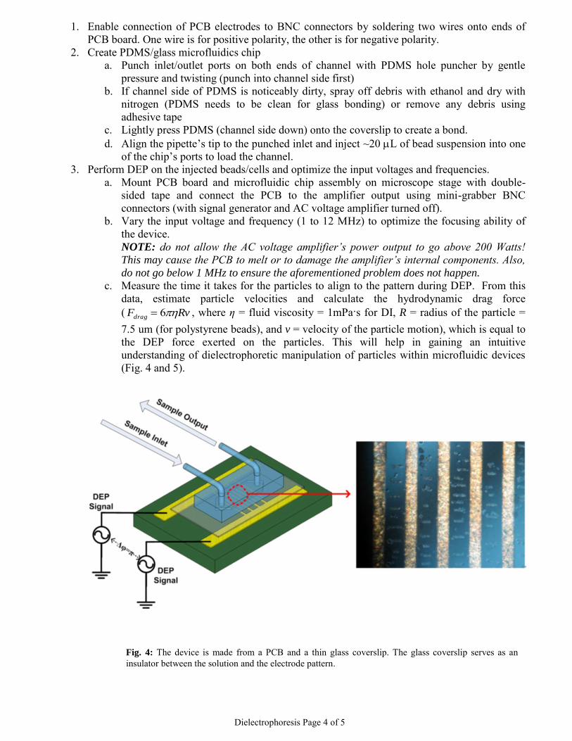