Embed Size (px)
Citation preview
THE UNIVERSITY
OF BIRMINGHAM
MICROMACHINED MICROWAVE FILTERS
by
Ignacio Llamas Garro
A thesis submitted to the School of Engineering of
The University of Birmingham
for the degree of
DOCTOR OF PHILOSOPHY
School of Engineering
Department of Electronic, Electrical and Computer Engineering
The University of Birmingham
April 2003
University of Birmingham Research Archive
e-theses repository This unpublished thesis/dissertation is copyright of the author and/or third parties. The intellectual property rights of the author or third parties in respect of this work are as defined by The Copyright Designs and Patents Act 1988 or as modified by any successor legislation. Any use made of information contained in this thesis/dissertation must be in accordance with that legislation and must be properly acknowledged. Further distribution or reproduction in any format is prohibited without the permission of the copyright holder.
2
Abstract
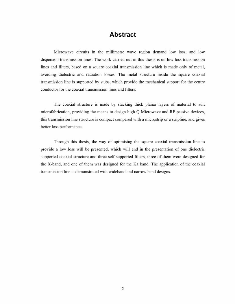
Microwave circuits in the millimetre wave region demand low loss, and low
dispersion transmission lines. The work carried out in this thesis is on low loss transmission
lines and filters, based on a square coaxial transmission line which is made only of metal,
avoiding dielectric and radiation losses. The metal structure inside the square coaxial
transmission line is supported by stubs, which provide the mechanical support for the centre
conductor for the coaxial transmission lines and filters.
The coaxial structure is made by stacking thick planar layers of material to suit
microfabrication, providing the means to design high Q Microwave and RF passive devices,
this transmission line structure is compact compared with a microstrip or a stripline, and gives
better loss performance.
Through this thesis, the way of optimising the square coaxial transmission line to
provide a low loss will be presented, which will end in the presentation of one dielectric
supported coaxial structure and three self supported filters, three of them were designed for
the X-band, and one of them was designed for the Ka band. The application of the coaxial
transmission line is demonstrated with wideband and narrow band designs.
3
To my family,
Ignacio, Nora and Maria Elena
4
Acknowledgments
I am very grateful to Professor Michael J. Lancaster for supervising this thesis, for
sharing his knowledge and enthusiasm for microwaves, and for his support and
encouragement during this period of work. I would also like to thank Professor Peter S. Hall
for getting me started in this PhD, for providing a nice working place to carry out this work,
and for his useful discussions.
Many thanks to Dr. Benjamin Carrión, Dr. Alonso Corona, Dr. Demian Hinojosa and
Rosana Marques for all the great moments that we had together, from the very beginning to
the end of this project. This would have not been the same without them.
I would like to thank my colleagues and members of the EDT and CE groups, for their
companionship and useful discussions. Thanks to Peng Jin and Dr. Kyle Jiang in Mechanical
Engineering for the fabrication of the SU8 pieces. Thanks to the outstanding work of Warren
Hay responsible for the fabrication of the X band filters, thanks to Clifford Ansell for the
fabrication of the brass box and for helping me ensemble the Ka band filter, and thanks to
Adnam Zentani for machining the resonators.
Finally I would like to thank the National Council for Science and Technology
(CONACYT) in Mexico for partially funding this PhD, along with my dear parents Dr.
Ignacio Llamas Huitrón and Dr. Nora Garro Bordonaro for always being so generous.
5
Index CHAPTER ONE: INTRODUCTION 14 1.1. CONTENTS OF THE THESIS 14 1.2. LMDS 18 1.3. REFERENCES 20 CHAPTER TWO: LITERATURE REVIEW 21 2.1. INTRODUCTION 21 2.2. A SQUARE COAXIAL TRANMSMISSION LINE 22 2.3. MICROMACHINED TRANSMISSION LINES AND RESONATORS 23 2.4. MICROMACHINED MIRCOWAVE FILTERS 32
2.4.1 INTRODUCTION 32 2.4.2 MICROMACHINED CAVITY RESONATORS AND FILTERS 32 2.4.3 LIGA PLANAR TRANSMISSION LINES AND FILTERS 35 2.4.4 MEMBRANE SUPPORTED FILTERS 38 2.4.5 A HIGH Q MILLIMETRE WAVE DILECTRIC RESONATOR 41 2.4.6 MICROMACHINED FILTERS ON SYNTHESIZED
SUBSTRATES 42 2.4.7 MICROMACHINED TUNABLE FILTERS 45
2.5. REFERENCES 48 CHAPTER THREE: TRANSMISSION LINE THEORY 52 3.1 INTRODUCTION 52 3.2 THE TELEGRAPHER EQUATIONS 53 3.3 STANDING WAVES 58
3.3.1 THE QUARTER WAVE TRANSFORMER 62 3.3.2 A HALFWAVELENGTH TRANSMISSION LINE
TERMINATED IN AN OPEN CIRCUIT 63 3.4 WAVE PROPAGATION 65
3.4.1 THE WAVE EQUATION 65 3.4.2 TEM AND QUASI TEM MODES 68 3.4.3 DISPERSION 70
3.5 BASIC MICROWAVE TRANSMISSION LINES 71 3.6 CONCLUSIONS 76 3.7 REFERENCES 77 CHAPTER FOUR: MICROWAVE RESONATORS 78 4.1. INTRODUCTION 78 4.2. THE UNLOADED QUALITY FACTOR 79
4.2.1. SERIES RESONANCE 79 4.2.2 PARALLEL RESONANCE 82
4.3. UNLOADED QUALITY FACTOR OF A HALF WAVELENGTH TRANSMSISSION LINE RESONATOR 83
4.4. MATERIAL LOSSES 87 4.4.1 CONDUCTOR LOSS 90
4.5. EXTRACTING Q FROM MEASUREMENTS 94
6
4.6. FINDING QO USING CAD 97 4.7. CONCLUSIONS 99 4.8. REFERENCES 100 CHAPTER FIVE: GENERAL FILTER DESIGN 102 5.1. INTRODUCTION 102 5.2. THE LOW PASS PROTOTYPE 103 5.3. NARROW BAND COUPLED RESONATOR BANDPASS FILTERS 107
5.3.1 BANDPASS TRANSFORMATION 107 5.3.2 FILTERS USING IMPEDANCE OR
ADMITTANCE INVERTERS 109 5.3.3 OBTAINING THE DESIGN PARAMETERS FOR A
BANDPASS DISTRIBUTED ELEMENT FILTER FROM THE LOW PASS PROTOTYPE 114
5.3.4 DETERMINATION OF COUPLINGS WITH THE AID OF A CAD SIMULATOR 115 5.3.4.1 CALCULATING Qe 116 5.3.4.2 CALCULATING THE COUPLINGS
BETWEEN RESONATORS 117 5.4. WIDEBAND FILTER USING QUARTER WAVELENGTH STUBS 121 5.5. EXTRACTING Qo FROM AN EXPERIMENTAL FILTER 123 5.6. CONCLUSIONS 124 CHAPTER SIX: MICROMACHINED TRANSMISSION LINES
AND RESONATORS 126 6.1. INTRODUCTION 126 6.2. THE SEARCH FOR A HIGH Q TRANSMISSION LINE 127
6.2.1 THE SHELDED MICROSTRIP RESONATOR 127 6.2.2 THE PARALLEL PLATE WAVEGUIDE 129 6.2.3 THE DEEP COPLANAR WAVEGUIDE 132 6.2.4 A SQUARE COAXIAL RESONATOR 133
6.3. ANALYTICAL LOSS COMPARISON OF LOW LOSS TRANSMISSION LINES 135 6.3.1 LOW LOSS TRANSMISSION LINES 135 6.3.2 LOSS CALCULATION 137 6.3.3 LOSS COMPARISON 141
6.4. CONCLUSIONS 143 6.5. REFERENCES 144 CHAPTER SEVEN: SQUARE COAXIAL MICROWAVE
BANDPASS FILTERS 145 7.1. INTRODUCTION 145 7.2. X BAND NARROW BAND FILTER 146
7.2.1. DESIGN PARAMETERS 146 7.2.2. FILTER ASSEMBLY AND TECHNICAL DRAWINGS 149 7.2.3. TUNING 152 7.2.4. RESPONSE 153 7.2.5. U-BAND FILTERS 155
7
7.2.5.1. TECHNICAL DRAWINGS 156 7.2.5.2. SIMULATED RESPONSES 159
7.3. X BAND WIDEBAND FILTER 161 7.3.1. DESIGN PARAMETERS 163 7.3.2. FILTER ASSEMBLY AND TECHNICAL DRAWINGS 164 7.3.3. RESPONSE 166
7.4. X BAND DUAL MODE FILTER 168 7.4.1. THE DUAL MODE RESONATOR 169 7.4.2. DESIGN PARAMETERS 170 7.4.3. THE FEED 173 7.4.4. FILTER ASSEMBLY AND TECHNICAL DRAWINGS 174 7.4.5. RESPONSE 177
7.5. KA BAND DUAL MODE MICROMACHINED FILTER 179 7.5.1. DESIGN PARAMETERS 180 7.5.2. THE FEED 181 7.5.3. FILTER ASSEMBLY AND TECHNICAL DRAWINGS 182 7.5.4. LASER MICROMACHINED FILTER 185 7.5.5 RESPONSE 189
7.6. CONCLUSIONS 190 7.7. REFERENCES 190 CHAPTER EIGHT: CONCLUSIONS AND FURTHER WORK 191 8.1. CONCLUSIONS 191 8.2. FURTHER WORK 192 APENDIX: LIST OF PUBLICATIONS 197

8
Glossary of abbreviations
BCB - Benzocyclobutene
CAD – Computer Aided Design
ECPW – Elevated Coplanar transmission line
IC – Integrated Circuit
IMSL – Inverted Microstrip Line
LIGA – German acronym with an English translation of Lithography, Electroforming and
Moulding
LMDS – Local Multipoint Distribution System
MEMS – Micro Electro-Mechanical Systems
MMIC – Monolithic Microwave Integrated Circuit
MOPA – Master Oscillator Power Amplifier
OCPW – Overlay Coplanar transmission line
SU8 – Organic Photosensitive Resin
TEM – Transverse Electromagnetic Mode
Approximate Band designations
X- Band 8-12 GHz
Ka- Band 26-40 GHz
U- Band 40-60 GHz
W- Band 60-100 GHz
9
List of Figures CHAPTER ONE: INTRODUCTION Figure 1-1 Diagram of the experiments in this research 18 Figure 1-2 A five sectored LMDS cell 20 CHAPTER TWO: LITERATURE REVIEW Figure 2-1 A square coaxial transmission line 22 Figure 2-2 Side view of the X band micromachined resonator 33 Figure 2-3 Side view of the three-cavity filter 34 Figure 2-4 Measured and simulated response for the three cavity filter 34 Figure 2-5 Two coupled LIGA microstrip lines 35 Figure 2-6 The LIGA 14 GHz low pass filter 36 Figure 2-7 The LIGA 10 GHz bandpass filter 37 Figure 2-8 Layout of the 4 pole membrane quasi elliptic filter 38 Figure 2-9 Measured response of the 4 pole membrane quasi elliptic filter 39 Figure 2-10 Layout of the K-band diplexer 40 Figure 2-11 Response of the K band diplexer 41 Figure 2-12 A dielectric resonator at millimetre waves 42 Figure 2-13 Micromachined filters on synthesized substrates 43 Figure 2-14 Seven section Chebyshev filter on a synthesized substrate 44 Figure 2-15 Varactor tuned X band filter 45 Figure 2-16 Measured response of the varactor tuned X band filter 46 Figure 2-17 Micrograph of the two micromachined tunable filters 47 Figure 2-18 Measured responses of the two micromachined tunable filters 48 CHAPTER THREE: TRANSMISSION LINE THEORY Figure 3-1 Short length of transmission line 54 Figure 3-2 Variation in phase of a travelling wave 56 Figure 3-3 Lossless transmission line terminated in a load impedance 58 Figure 3-4 Phasor diagram for the incident and reflected voltages 60 Figure 3-5 The quarter wave transformer 62 Figure 3-6 Electromagnetic wave travelling in the positive z direction 69 Figure 3-7 Microstrip 71 Figure 3-8 The coplanar line 71 Figure 3-9 Slotline 72 Figure 3-10 Stripline 72 Figure 3-11 Parallel plate waveguide 73 Figure 3-12 Coaxial line 73 Figure 3-13 Slabline 74 Figure 3-14 Two wires 74 Figure 3-15 Waveguide 75 Figure 3-16 Ridge waveguide 75 Figure 3-17 Dielectric waveguide 76
10
CHAPTER FOUR: MICROWAVE RESONATORS Figure 4-1 Series resonant circuit 79 Figure 4-2 Parallel resonant circuit 82 Figure 4-3 Loss tangent 89 Figure 4-4 Section of a conductor illustrating the decay of current 91 Figure 4-5 Microwave resonant cavity 94 Figure 4-6 Frequency response of a single resonator 96 Figure 4-7 Cross section of a square coaxial resonator 97 Figure 4-8 Square coaxial resonator QO 98 Figure 4-9 Presence of higher modes in a square coaxial transmission line 99 CHAPTER FIVE: GENERAL FILTER DESIGN Figure 5-1 Chebyshev low pass prototype response 103 Figure 5-2 Low pass prototype filer 105 Figure 5-3 Bandpass response 107 Figure 5-4 Bandpass filter transformation 108 Figure 5-5 Conversions using impedance or admittance inverters 110 Figure 5-6 Band pass filter using impedance inverters and only series resonators 111 Figure 5-7 Lumped element impedance inverters 112 Figure 5-8 Band pass filter using admittance inverters and only shunt resonators 112 Figure 5-9 Lumped element admittance inverters 113 Figure 5-10 Design parameters of a bandpass filter 114 Figure 5-11 Extracting Qe from simulations 116 Figure 5-12 Typical S21 simulated response for Qe 117 Figure 5-13 Theoretical lumped element model for the electric coupling 118 Figure 5-14 Extracting the coupling between resonators from simulations 120 Figure 5-15 Typical S21 simulated response for two coupled resonators 120 Figure 5-16 Wideband filter using quarter wavelength stubs and quarter
wavelength connecting lines 122 Figure 5-17 Theoretical model used to extract QO from filter measurements 124 CHAPTER SIX: MICROMACHINED TRANSMISSION LINES AND RESONATORS Figure 6-1 Half wavelength resonator on a foam-duroid substrate 128 Figure 6-2 Microstrip transmission line 129 Figure 6-3 Aluminium parallel plate transmission line 130 Figure 6-4 Parallel plate transmission line 131 Figure 6-5 Deep coplanar waveguide 133 Figure 6-6 Square coaxial resonator 134 Figure 6-7 Low loss transmission lines 136 Figure 6-8 Transmission line cross section areas 141 Figure 6-9 Attenuation constant versus area 142 Figure 6-10 Qo versus area 143
11
CHAPTER SEVEN: SQUARE COAXIAL MICROWAVE BANDPASS FILTERS Figure 7-1 Extracting Qe for the narrowband X-band filter 147 Figure 7-2 Qe for the narrowband X-band filter 148 Figure 7-3 Extracting kc for the narrowband X-band filter (top view) 148 Figure 7-4 kc for the narrowband X-band filter 149 Figure 7-5 Assembly for the narrowband X-band filter 150 Figure 7-6 Technical drawings of the narrowband X-band filter 151 Figure 7-7 Tuning the narrowband X band filter (side view) 152 Figure 7-8 Frequency shift produced while tuning a single resonator for the
narrowband X band filter 153 Figure 7-9 Bandpass response of the narrowband X band filter 154 Figure 7-10 Photo of the narrowband X band filter 155 Figure 7-11 Technical drawings of the narrowband 40 GHz filter 157 Figure 7-12 Technical drawings of the narrowband 60 GHz filter 159 Figure 7-13 Simulated response of the 40 GHz bandpass filter 160 Figure 7-14 Simulated response of the 60 GHz bandpass filter 161 Figure 7-15 Main body of the wideband X band filter 162 Figure 7-16 Design parameters for the wideband X band filter 163 Figure 7-17 Filter assembly for the wideband X band filter 164 Figure 7-18 Technical drawings of the wideband X band filter 166 Figure 7-19 Bandpass response of the wideband X band filter 167 Figure 7-20 Photo of the wideband X band filter 168 Figure 7-21 Current flow on the dual mode resonator at resonance 169 Figure 7-22 Equivalent circuit of the dual mode resonator, modelled as
two coupled quarter wavelength resonators 170 Figure 7-23 Setting the coupling between the two modes of the
dual mode resonator 170 Figure 7-24 Setting the coupling for the dual mode X band resonator with B fixed 171 Figure 7-25 Setting the coupling for the dual mode X band resonator with A fixed 172 Figure 7-26 Finding Qe for the dual mode X band filter 172 Figure 7-27 Feed of the dual mode filter 173 Figure 7-28 Simulated response of the feed for the dual mode X band filter 174 Figure 7-29 Filter assembly of the dual mode X band filter 175 Figure 7-30 Technical drawings of the dual mode X band filter 177 Figure 7-31 Bandpass response of the dual mode X band filter 178 Figure 7-32 Photo of the dual mode X band filter 179 Figure 7-33 Setting the coupling for the dual mode Ka band
resonator with B fixed 180 Figure 7-34 Setting the coupling for the dual mode Ka band
resonator with A fixed 181 Figure 7-35 Simulated response of the feed for the dual mode Ka band filter 182 Figure 7-36 K connector assembly for the Ka band dual mode filter (side view) 183 Figure 7-37 Filter assembly of the dual mode Ka band filter 183 Figure 7-38 Technical drawings of the dual mode Ka band filter 185 Figure 7-39 Main layers of the Ka band dual mode micromachined filter 186 Figure 7-40 Brass box for the Ka band dual mode filter 187 Figure 7-41 Photo of the Ka band dual mode filter 188 Figure 7-42 Bandpass response of the dual mode Ka band filter 189
12
CHAPTER EIGHT: CONCLUSIONS AND FURTHER WORK Figure 8-1 MOPA (Master Oscillator Power Amplifier) system 194 Figure 8-2 SU8 Ka band dual mode filter 195 Figure 8-3 SU8 used as a mould to produce the circuit layers 196
13
List of Tables
CHAPTER ONE: INTRODUCTION Table 1-1 Notation used in this thesis 15 Table 1-2 Specification of the Ka band dual mode filter 19 CHAPTER TWO: LITERATURE REVIEW Table 2-1 Micromachined transmission lines 29 Table 2-2 synthesized High-Impedance (HI) design parameters on
full thickness silicon and micromachined high-impedance sections based on a 10%:90% ratio of Si – air regions 44
CHAPTER SEVEN: SQUARE COAXIAL MICROWAVE BANDPASS FILTERS Table 7-1 Design parameters for the narrow band X band filter 146 Table 7-2 Design parameters for the wideband X band filter 162 Table 7-3 Design parameters for the narrow band dual mode filters 169
I.Llamas-Garro, PhD thesis (2003), The University of Birmingham, UK
1. CHAPTER ONE INTRODUCTION
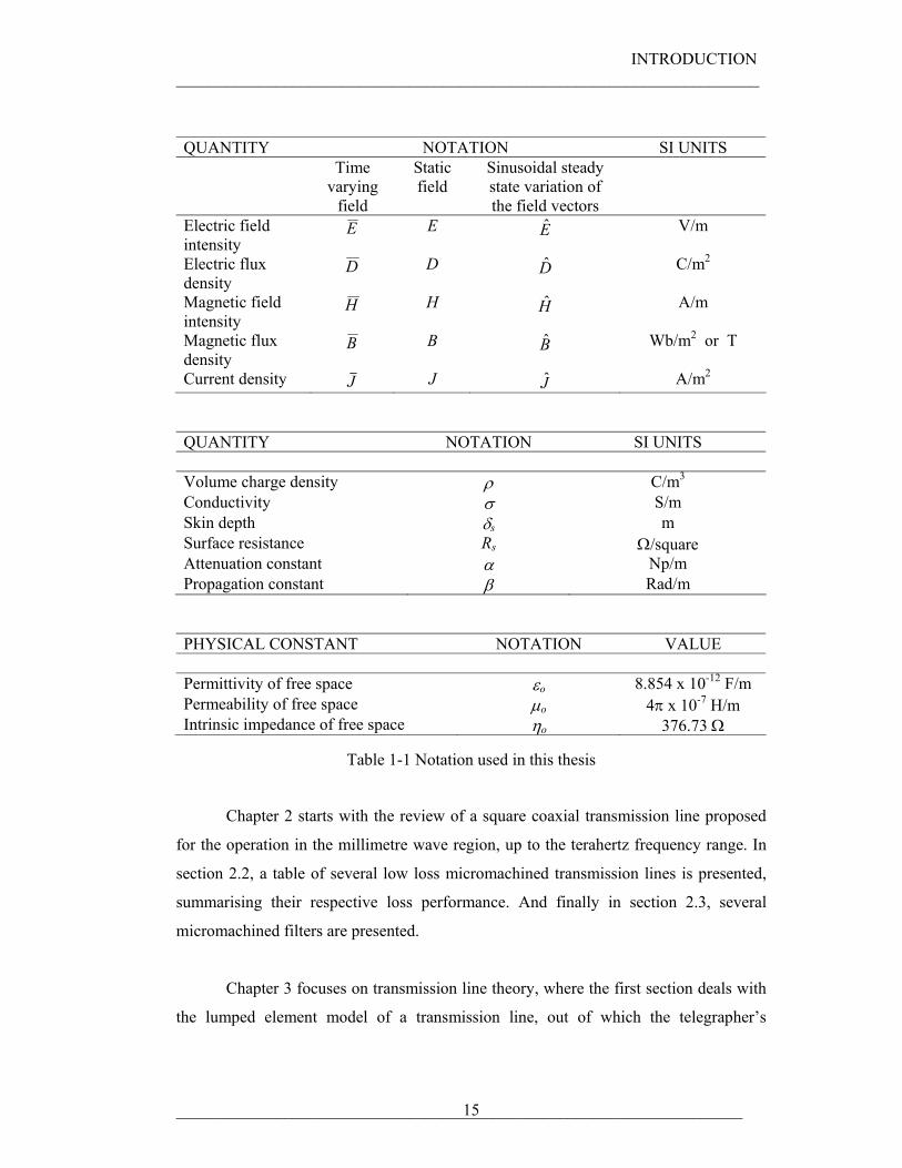
1.1. CONTENTS OF THE THESIS
The objective of this Chapter is to introduce each chapter of this thesis, as well
discuss the potential application of the Ka band dual mode filter discussed further in
Chapter 7, section 7.5.
Chapter 2 contains a literature review on micromachined transmission lines,
resonators and filters, followed by Chapters 3, 4 and 5 which describe the theory used in
the development of the resonators and filters discussed in Chapters 6 and 7; the notation
in Table 1-1 will be used throughout the theory chapters. Chapter 8 contains the overall
conclusions of this research and some proposals for further work. In the following
paragraphs there will be a description of the contents by chapter to give an overview of
the contents of this thesis.
INTRODUCTION ______________________________________________________________________
____________________________________________________________________ 15
QUANTITY NOTATION SI UNITS Time
varying field
Static field
Sinusoidal steady state variation of the field vectors
Electric field intensity
E E E V/m
Electric flux density
D D D C/m2
Magnetic field intensity
H H H A/m
Magnetic flux density
B B B Wb/m2 or T
Current density J J J A/m2 QUANTITY NOTATION SI UNITS
Volume charge density ρ C/m3 Conductivity σ S/m Skin depth δs m Surface resistance Rs Ω/square Attenuation constant α Np/m Propagation constant β Rad/m
PHYSICAL CONSTANT NOTATION VALUE Permittivity of free space εo 8.854 x 10⁻¹² F/m Permeability of free space µo 4π x 10-7 H/m Intrinsic impedance of free space ηo 376.73 Ω
Table 1-1 Notation used in this thesis
Chapter 2 starts with the review of a square coaxial transmission line proposed
for the operation in the millimetre wave region, up to the terahertz frequency range. In
section 2.2, a table of several low loss micromachined transmission lines is presented,
summarising their respective loss performance. And finally in section 2.3, several
micromachined filters are presented.
Chapter 3 focuses on transmission line theory, where the first section deals with
the lumped element model of a transmission line, out of which the telegrapher’s
INTRODUCTION ______________________________________________________________________
____________________________________________________________________ 16
equations will be derived. These equations are general and relate voltages and currents
on the transmission line to any point in time and space. Section 3.3, treats standing
waves, and ends with the input impedance of a low loss, half wavelength transmission
line terminated in an open circuit, which will be a useful result for the calculation of the
unloaded quality factor of a half wavelength transmission line resonator in Chapter 4. In
section 3.4, wave propagation is discussed, followed by the definition of the TEM
(Transverse Electromagnetic Mode) mode, and dispersion problems in transmission
lines. Finally, at the end of the chapter, basic transmission lines used in microwave
engineering will be presented.
In Chapter 4, resonator theory is reviewed; resonators are used in frequency
selective devices, like filters, oscillators or frequency measurement devices. Section 4.2
contains a description of lumped element resonant circuits. In section 4.3, the formula to
calculate the unloaded quality factor for a half wavelength distributed element resonator
will be derived. Section 4.4 treats material losses, especially the conductor loss, since
the main structures used in this thesis are conductor loss limited transmission lines.
Section 4.5 contains a practical way of extracting the unloaded quality factor directly
from experimental measurements, and finally in section 4.6, the unloaded quality factor
for a square coaxial resonator is discussed.
Chapter 5 contains the theory used to design the bandpass filters presented in
Chapter 7. Section 5.2 contains a discussion of the low pass filter prototype, which will
be converted to give a bandpass response in section 5.3; where narrowband coupled
resonator filters will be addressed. The rest of section 5.3 contains the theory on how to
develop a practical Chebyschev bandpass filter with the aid of a CAD simulator.
Section 5.4, contains the design formulae for a wideband bandpass filter using quarter
wavelength stubs as resonators, with quarter wavelength transmission lines connecting
the resonators. Finally in section 5.5, a method of extracting the unloaded quality factor
from experimental filter measurements will be presented; as well as a formula to
calculate the insertion loss of a practical filter assuming that the resonator’s unloaded
quality factor is known.
INTRODUCTION ______________________________________________________________________
____________________________________________________________________ 17
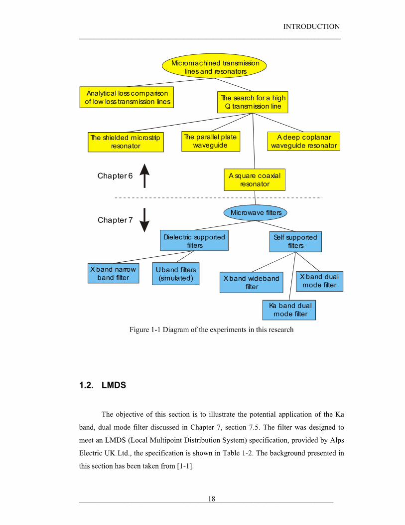
Chapter 6 contains the first experiments that were carried out in order to define a
good transmission line to make the filters discussed in Chapter 7. These experiments
start with a shielded microstrip line, followed by a parallel plate waveguide, and a deep
coplanar waveguide, and finally the square coaxial transmission line, as shown in
Figure 1-1. Section 6.3 contains an analytical loss comparison of four different
transmission lines, which include the microstrip, the stripline, the round coaxial line and
the square coaxial line.
Chapter 7 is divided into two parts, Part I contains filters which were designed
using a coaxial structure, with its centre conductor supported with a bar of dielectric,
and Part II contains filters, which were designed using all metal structures that have an
air propagation media, enhancing filter performance by avoiding substrate losses. The
link between Chapters 6 and 7 is shown in Figure 1-1.
Finally Chapter 8 contains the overall conclusions on this research, as well as
some proposed further work, which is mainly focused on different ways of producing
the square coaxial filters of Chapter 7, and the possibilities of creating new filters or
transmission line architectures using self supported metals.
INTRODUCTION ______________________________________________________________________
____________________________________________________________________ 18
X band narrowband filter
Micromachined transmission lines and resonators
Analytical loss comparisonof low loss transmission lines The search for a high
Q transmission line
The shielded microstripresonator
The parallel platewaveguide
A deep coplanarwaveguide resonator
A square coaxialresonator
Microwave filters
Dielectric supportedfilters
U band filters(simulated)
Self supported filters
X band widebandfilter
X band dual mode filter
Ka band dualmode filter
Chapter 6
Chapter 7
Figure 1-1 Diagram of the experiments in this research
1.2. LMDS
The objective of this section is to illustrate the potential application of the Ka
band, dual mode filter discussed in Chapter 7, section 7.5. The filter was designed to
meet an LMDS (Local Multipoint Distribution System) specification, provided by Alps
Electric UK Ltd., the specification is shown in Table 1-2. The background presented in
this section has been taken from [1-1].
INTRODUCTION ______________________________________________________________________
____________________________________________________________________ 19
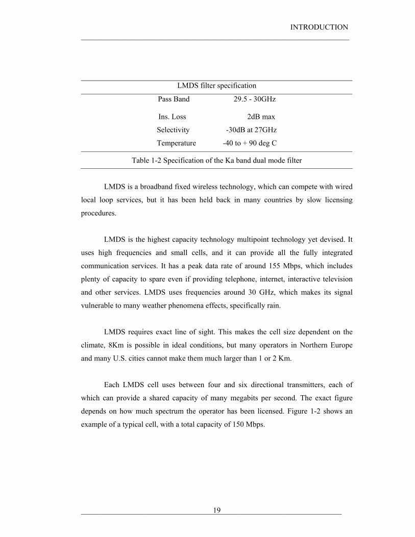
LMDS filter specification
Pass Band 29.5 - 30GHz
Ins. Loss 2dB max
Selectivity -30dB at 27GHz
Temperature -40 to + 90 deg C
Table 1-2 Specification of the Ka band dual mode filter
LMDS is a broadband fixed wireless technology, which can compete with wired
local loop services, but it has been held back in many countries by slow licensing
procedures.
LMDS is the highest capacity technology multipoint technology yet devised. It
uses high frequencies and small cells, and it can provide all the fully integrated
communication services. It has a peak data rate of around 155 Mbps, which includes
plenty of capacity to spare even if providing telephone, internet, interactive television
and other services. LMDS uses frequencies around 30 GHz, which makes its signal
vulnerable to many weather phenomena effects, specifically rain.
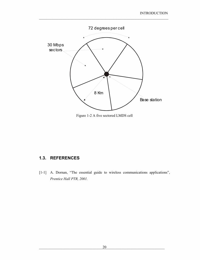
LMDS requires exact line of sight. This makes the cell size dependent on the
climate, 8Km is possible in ideal conditions, but many operators in Northern Europe
and many U.S. cities cannot make them much larger than 1 or 2 Km.
Each LMDS cell uses between four and six directional transmitters, each of
which can provide a shared capacity of many megabits per second. The exact figure
depends on how much spectrum the operator has been licensed. Figure 1-2 shows an
example of a typical cell, with a total capacity of 150 Mbps.
INTRODUCTION ______________________________________________________________________
____________________________________________________________________ 20
Base station
30 Mbpssectors
72 degrees per cell
8 Km
Figure 1-2 A five sectored LMDS cell
1.3. REFERENCES
[1-1] A. Dornan, “The essential guide to wireless communications applications”,
Prentice Hall PTR, 2001.
I.Llamas-Garro, PhD thesis (2003), The University of Birmingham, UK
2. CHAPTER TWO
LITERATURE REVIEW
2.1. INTRODUCTION
The study of low loss and low dispersion transmission lines is the first step
towards developing a high performance millimetre wave filter. As the design frequency
gets higher, the circuit dimensions shrink inversely proportional to frequency, and the
skin effect resistance increases approximately proportional to the square root of
frequency.
This chapter starts with the presentation of a square coaxial transmission line
proposed for millimetre wave integrated circuits, followed by a table in section 2.3,
containing several transmission lines and resonators, each with its respective attenuation
constant and unloaded quality factor for a half wavelength resonator made out of its
respective structure. Finally in section 2.4 there is a review on micromachined filters.
LITERATURE REVIEW ______________________________________________________________________
____________________________________________________________________ 22
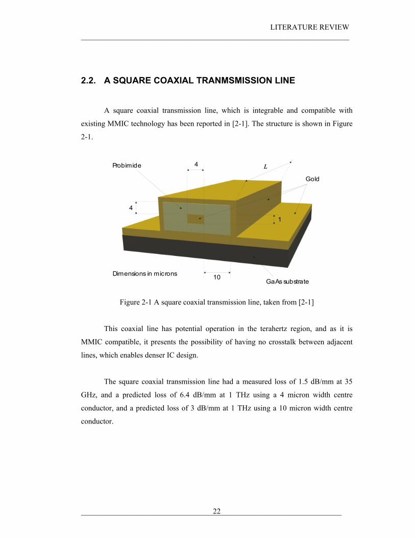
2.2. A SQUARE COAXIAL TRANMSMISSION LINE
A square coaxial transmission line, which is integrable and compatible with
existing MMIC technology has been reported in [2-1]. The structure is shown in Figure
2-1.
L
4
10
1
4
Dimensions in microns
Gold
GaAs substrate
Probimide
Figure 2-1 A square coaxial transmission line, taken from [2-1]
This coaxial line has potential operation in the terahertz region, and as it is
MMIC compatible, it presents the possibility of having no crosstalk between adjacent
lines, which enables denser IC design.
The square coaxial transmission line had a measured loss of 1.5 dB/mm at 35
GHz, and a predicted loss of 6.4 dB/mm at 1 THz using a 4 micron width centre
conductor, and a predicted loss of 3 dB/mm at 1 THz using a 10 micron width centre
conductor.
LITERATURE REVIEW ______________________________________________________________________
____________________________________________________________________ 23
2.3. MICROMACHINED TRANSMISSION LINES AND RESONATORS
Several transmission lines and resonators taken from several publications are
shown in Table 2-1. The experimental results for each reference is resumed as the total
loss, and the QO for a half wavelength resonator made out of its respective transmission
line architecture.
LITERATURE REVIEW ______________________________________________________________________
____________________________________________________________________ 24
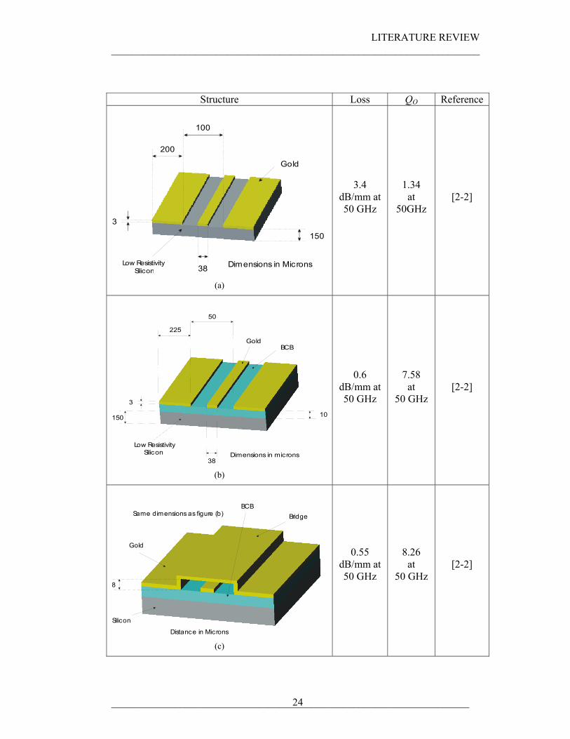
Structure Loss QO Reference
100
200
38
150
3
Low Resistivity Silicon
Gold
Dimensions in Microns
(a)
3.4 dB/mm at 50 GHz
1.34 at
50GHz
[2-2]
50
225
10
38
150
3
Low Resistivity Silicon
BCB
Dimensions in microns
Gold
(b)
0.6 dB/mm at 50 GHz
7.58 at
50 GHz
[2-2]
8
Distance in Microns
Same dimensions as figure (b) Bridge
Gold
BCB
Silicon
(c)
0.55 dB/mm at 50 GHz
8.26 at
50 GHz
[2-2]
LITERATURE REVIEW ______________________________________________________________________
____________________________________________________________________ 25
300
3
380
Distances in microns
Silicon
Gold
(d)
0.15 dB/mm at 40 GHz
24 at
40 GHz
[2-3]
Distances in Microns
300
380200
Air gap
3
Silicon
Gold
(e)
0.12 dB/mm at 40 GHz
30 at
40 GHz
[2-3]
1) 1002) 0
3
300
20
Distances in microns
200
Silicon
BCBGold
(f)
1) 0.06
dB/mm at 40 GHz
2) 0.033
dB/mm at 40 GHz
1) 60 at
40 GHz 2)
110 at
40 GHz
[2-3]
LITERATURE REVIEW ______________________________________________________________________
____________________________________________________________________ 26
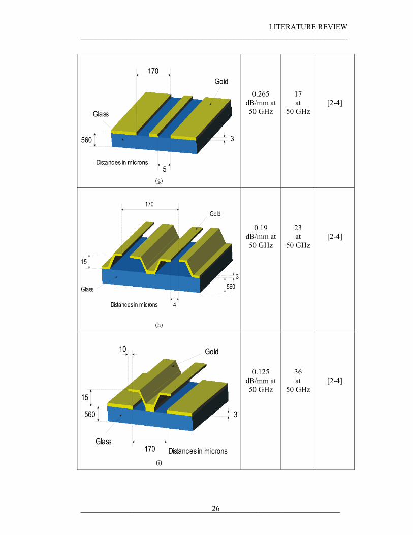
170
5
3560
Distances in microns
Glass
Gold
(g)
0.265 dB/mm at 50 GHz
17 at
50 GHz
[2-4]
15
5603
170
4Distances in microns
Glass
Gold
(h)
0.19 dB/mm at 50 GHz
23 at
50 GHz
[2-4]
3
170
10
15
560
Distances in microns
Gold
Glass
(i)
0.125 dB/mm at 50 GHz
36 at
50 GHz
[2-4]
LITERATURE REVIEW ______________________________________________________________________
____________________________________________________________________ 27
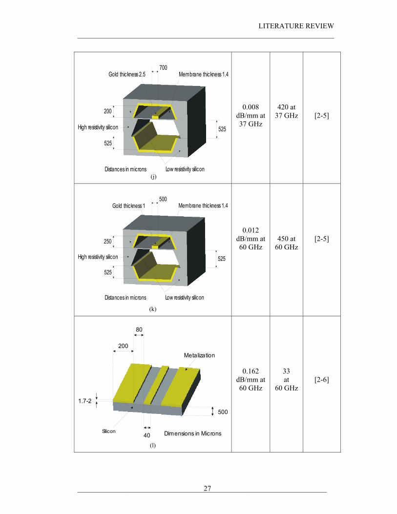
700
Membrane thickness 1.4Gold thickness 2.5
200
525
525
Low resistivity silicon
High resistivity silicon
Distances in microns (j)
0.008 dB/mm at 37 GHz
420 at 37 GHz
[2-5]
500
Membrane thickness 1.4Gold thickness 1
250
525
525
Low resistivity silicon
High resistivity silicon
Distances in microns
(k)
0.012 dB/mm at 60 GHz
450 at 60 GHz
[2-5]
80
200
40
500
1.7-2
Silicon
Metalization
Dimensions in Microns (l)
0.162 dB/mm at 60 GHz
33 at
60 GHz
[2-6]
LITERATURE REVIEW ______________________________________________________________________
____________________________________________________________________ 28
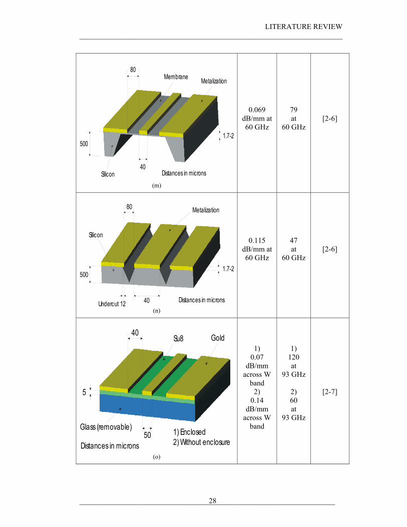
Distances in microns
Metalization
Silicon
Membrane80
40
5001.7-2
(m)
0.069
dB/mm at 60 GHz
79 at
60 GHz
[2-6]
80
40
1.7-2
Distances in micronsUndercut 12
500
Metalization
Silicon
(n)
0.115 dB/mm at 60 GHz
47 at
60 GHz
[2-6]
40
50
5
Su8
Glass (removable) 1) Enclosed2) Without enclosure
Gold
Distances in microns (o)
1) 0.07
dB/mm across W
band 2)
0.14 dB/mm
across W band
1) 120 at
93 GHz
2) 60 at
93 GHz
[2-7]
LITERATURE REVIEW ______________________________________________________________________
____________________________________________________________________ 29
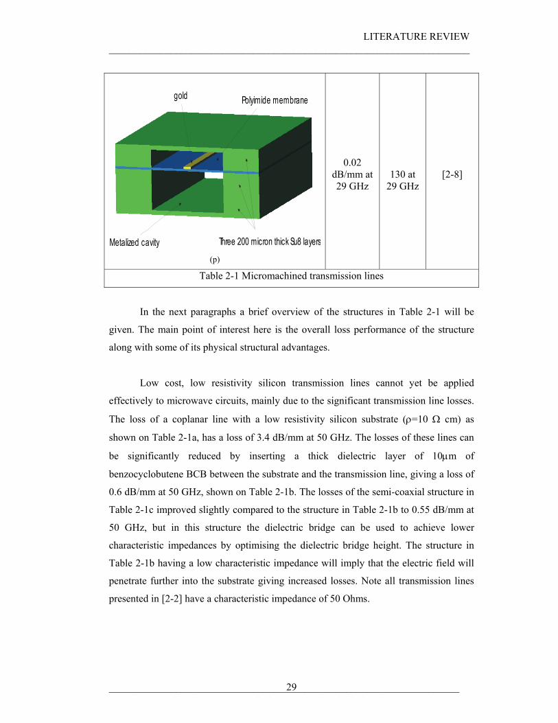
Three 200 micron thick Su8 layers
Polyimide membranegold
Metalized cavity(p)
0.02 dB/mm at 29 GHz
130 at 29 GHz
[2-8]
Table 2-1 Micromachined transmission lines
In the next paragraphs a brief overview of the structures in Table 2-1 will be
given. The main point of interest here is the overall loss performance of the structure
along with some of its physical structural advantages.
Low cost, low resistivity silicon transmission lines cannot yet be applied
effectively to microwave circuits, mainly due to the significant transmission line losses.
The loss of a coplanar line with a low resistivity silicon substrate (ρ=10 Ω cm) as
shown on Table 2-1a, has a loss of 3.4 dB/mm at 50 GHz. The losses of these lines can
be significantly reduced by inserting a thick dielectric layer of 10µm of
benzocyclobutene BCB between the substrate and the transmission line, giving a loss of
0.6 dB/mm at 50 GHz, shown on Table 2-1b. The losses of the semi-coaxial structure in
Table 2-1c improved slightly compared to the structure in Table 2-1b to 0.55 dB/mm at
50 GHz, but in this structure the dielectric bridge can be used to achieve lower
characteristic impedances by optimising the dielectric bridge height. The structure in
Table 2-1b having a low characteristic impedance will imply that the electric field will
penetrate further into the substrate giving increased losses. Note all transmission lines
presented in [2-2] have a characteristic impedance of 50 Ohms.
LITERATURE REVIEW ______________________________________________________________________
____________________________________________________________________ 30
The microstrip structure in Table 2-1d, is compared to the inverted microstrip
line (IMSL) of Table 2-1e in [2-3], where the simulated results gave a loss of 0.15
dB/mm at 40 GHz for the microstrip structure. By reducing the loss using the IMSL
which consists of two substrates bonded together and using the air gap formed between
the line and cavity to obtain a low loss transmission, the simulated result gave 0.12
dB/mm at 40 GHz. Finally the IMSL was modified to give additional low loss
characteristics by incorporating a membrane layer of BCB as shown on Table 2-1f.
Here the results gave a loss of 0.06 dB/mm at 40 GHz when using a 100 micron thick
silicon substrate below the membrane, and a loss of 0.033 dB/mm at 40 GHz when
using BCB only as a substrate.
The structures in reference [2-4] are all coplanar transmission lines on a glass
substrate. The first one, which is a conventional coplanar transmission line shown in
Table 2-1g, has a loss of 0.265 dB/mm at 50 GHz. The transmission line in Table 2-1h
is introduced as the elevated coplanar transmission line ECPW, this structure has a loss
of 0.19 dB/mm at 50 GHz, and finally the figure in Table 2-1i is introduced as the
overlay coplanar transmission line OCPW and has a loss of 0.125 dB/mm at 50 GHz.
These transmission lines use micromachining technology to elevate the metal lines from
the substrate reducing conductor and dielectric loss. The transmission lines compared
here have a characteristic impedance of 40 Ohms.
The use of membrane technology as in [2-5] allows a significant reduction of
loss. These circuits have a very good overall performance due to the thin membrane that
permits an air propagation media in a completely shielded structure. This structure also
allows the reduction of ohmic losses in the circuit, since it is possible to use wide
microstrips. A half wavelength resonator at 37 GHz made out of the structure in Table
2-1j has a loss of 0.008 dB/mm at 37 GHz, and a loss of 0.012 dB/mm at 60 GHz as
shown in Table 2-1k.
In the coplanar transmission lines exposed in [2-6] (Table 2-1m), the idea is to
use silicon micromachining to remove the dielectric material from the gap regions to
reduce dispersion and minimize the propagation loss. In coplanar lines, the field is
LITERATURE REVIEW ______________________________________________________________________
____________________________________________________________________ 31
tightly concentrated in the gaps between the conductors. When the material in this area
is removed, the line capacitance is reduced, leading to less current flow in the
conductors [2-6]. As a result, the line exhibits lower ohmic and dielectric loss. Here
three types of coplanar lines are compared: the first one on Table 2-1l shows a
conventional coplanar line on a high resistivity silicon wafer that has a loss of 0.162
dB/mm at 60 GHz, the next coplanar line is suspended by membrane technology and
has a loss of 0.069 dB/mm at 60 GHz, shown in Table 2-1m. Finally, the coplanar line
in Table 2-1n which has the material removed between conductors, with an undercut
below them, in this case 12 µm, has a loss of 0.115 dB/mm at 60 GHz.
A low cost membrane supported structure to realize planar printed circuits
compared to the membrane technology in [2-5] is demonstrated in [2-7]. Here the
membrane is made from a thin organic photosensitive resin SU8, this structure is
illustrated in Table 2-1o. This process allows active devices to be mounted on a
membrane of controllable thickness before removing the glass membrane backing. The
mechanical strength provided by the glass substrate minimizes mechanical damage to
the membrane when the active device is mounted. The coplanar structure has a loss of
0.07 dB/mm across W band under an enclosed environment, and a loss of 0.14 dB/mm
across W band without the enclosure, here a ≈500 nm gold metalization is used. On [2-
9], a method is reported that allows the use of higher conductivity metals like copper or
silver; with this technique a finline resonator was realized, having a loss of 0.074
dB/mm at 81.5 Ghz.
The structure in Table 2-1p has a similar form as the one in Table 2-1j or k. The
difference here is that SU8 is employed instead of silicon, the metalization is gold with
a thickness of 2-3 µm, and the polyimide membrane is 2-3 mil thick, and the entire
cavity walls are coated with gold. SU8 is very attractive for micromachining structures
with significant thickness and with high aspect ratios [2-8]. A half wavelength resonator
at 29 GHz has a loss of 0.02 dB/mm. The Qo value can be increased by having a higher
cavity. The process used to make this structure is considerably simpler than silicon
processing and presents a creative way to form more complicated shapes than those
achievable in silicon.
LITERATURE REVIEW ______________________________________________________________________
____________________________________________________________________ 32
The structure proposed in reference [2-5], is the one that presents the best
overall loss performance, regardless of its complex processing compared to other
structures like the ones presented in references [2-7], [2-8] and [2-9]. Transmission lines
with the lowest dispersion are the ones that have a uniform air propagation media,
compared to those that have one or more propagation medias, the dispersion of a
particular transmission line will depend on the field distribution of the particular line
and the propagation media used, the transmission lines with most dispersion are the
ones that have their fields confined through different materials with different dielectric
constants.
2.4. MICROMACHINED MIRCOWAVE FILTERS
2.4.1 INTRODUCTION
In this section there is a review of micromachined filters, with the objective of
showing different micromachined microwave filters designed by different technologies.
2.4.2 MICROMACHINED CAVITY RESONATORS AND FILTERS
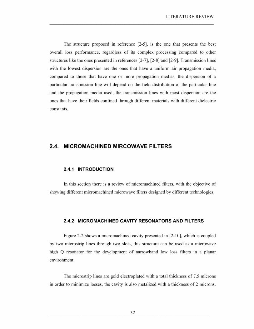
Figure 2-2 shows a micromachined cavity presented in [2-10], which is coupled
by two microstrip lines through two slots, this structure can be used as a microwave
high Q resonator for the development of narrowband low loss filters in a planar
environment.
The microstrip lines are gold electroplated with a total thickness of 7.5 microns
in order to minimize losses, the cavity is also metalized with a thickness of 2 microns.
LITERATURE REVIEW ______________________________________________________________________
____________________________________________________________________ 33
The cavity had a measured Q of 506 ± 55, which is very close to the theoretical value of
526 for a metallic cavity with the same dimensions.
32.354
0.5
0.465
Micromachined cavity
Microstrip feeds
Coupling slots
Dimensions in mm
Figure 2-2 Side view of the X band micromachined resonator, taken from [2-10]
A 10 GHz filter constructed of slot coupled micromachined cavities in silicon is
presented in [2-11]. The simulated model has a bandwidth of 4% with an insertion loss
of 0.9 dB at 10.02 GHz. The measured filter yields a 3.7% bandwidth with a
deembedded insertion loss of 2 dB at 10.01 GHz. The difference of loss is due to in part
to the CPW-microstrip transition and line lengths; also an equipment malfunction
during the bonding process caused an unexpected rapid raise in temperature, which
created a gold-silicon eutectic, which resulted in a reduction in conductivity of the gold.
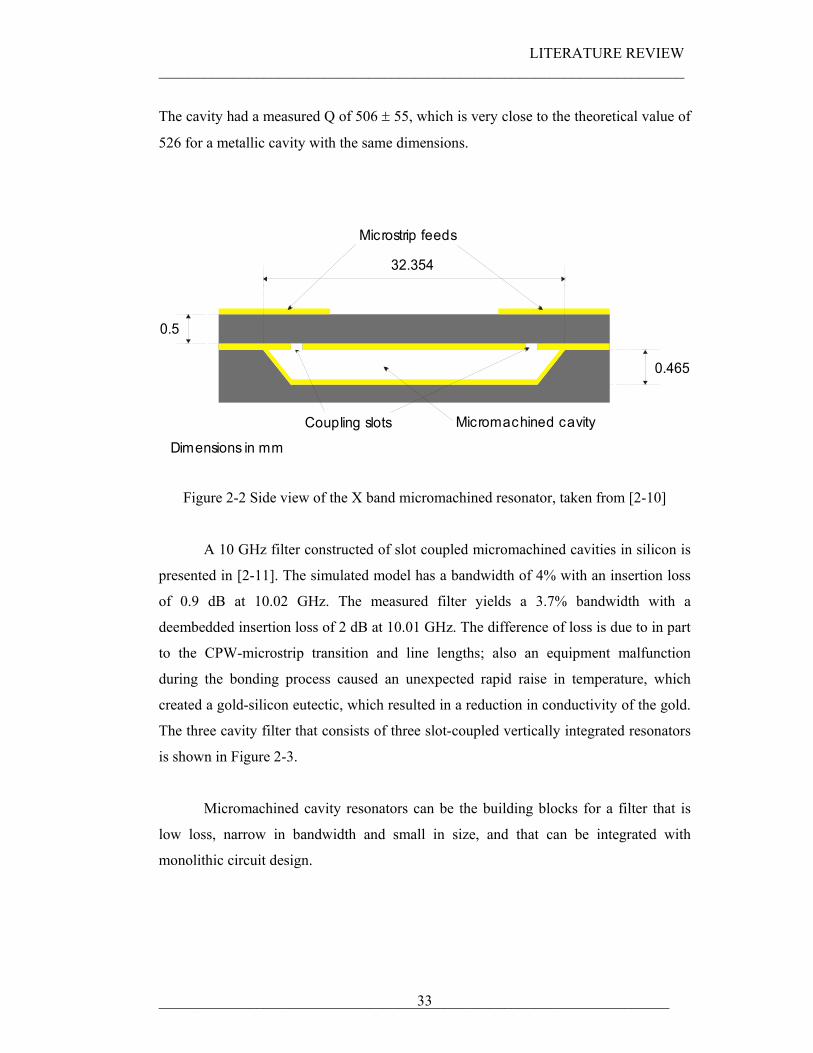
The three cavity filter that consists of three slot-coupled vertically integrated resonators
is shown in Figure 2-3.
Micromachined cavity resonators can be the building blocks for a filter that is
low loss, narrow in bandwidth and small in size, and that can be integrated with
monolithic circuit design.
LITERATURE REVIEW ______________________________________________________________________
____________________________________________________________________ 34
Microstrip feed
Microstrip feed
Probe
Probe
500 micron cavity wafers
100 micron slot wafers
500 micron wafer
400 micron wafer
CPW-slotline-microstrip transition
Slot/ground plane
Figure 2-3 Side view of the three-cavity filter, taken from [2-11]
A high Q filter constructed of these resonators yields high power handling
capabilities as the surface currents are distributed over a large conductor area. The
microstrip lines, CPW lines, and top and bottom wafer ground/slot planes are gold
electroplated to approximately 3 microns, and all surfaces of the etched slot and cavity
wafers are gold electroplated to a similar depth. The overall dimensions of the finished
filter are approximately 5 cm long x 3cm wide x 2600 micron high. The deembedded
measured and simulated response for the filter is shown in Figure 2-4.
10
0
-10
-20
-30
-40
-50
-609.00 9.25 9.50 9.75 10.00 10.25 10.50 10.75 11.00
S-Pa
ram
eter
s, dB
Frequency, Ghz
HFSS, S21
HFSS, S11
Measured, S11
De-embedded measured, S21
Figure 2-4 Measured and simulated response for the three cavity filter, taken from [2-11]
LITERATURE REVIEW ______________________________________________________________________
____________________________________________________________________ 35
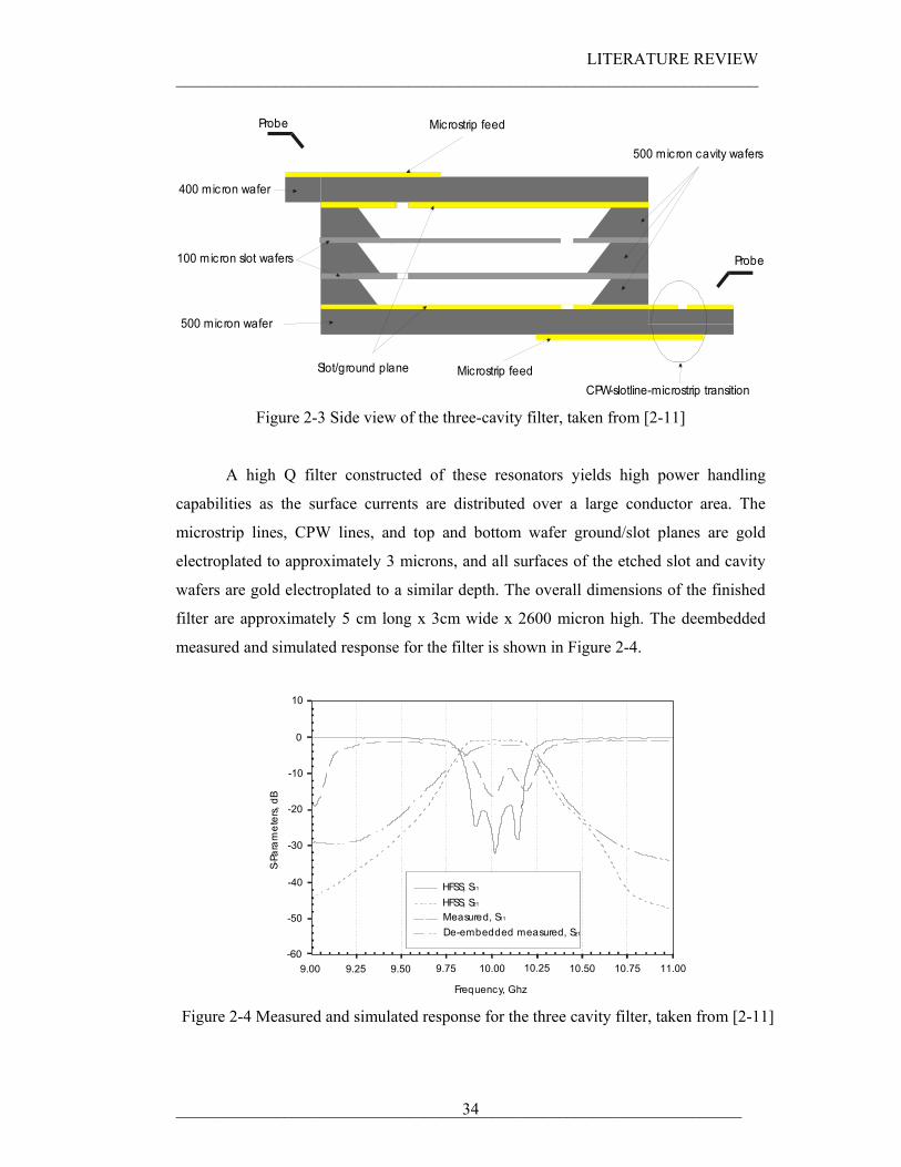
2.4.3 LIGA PLANAR TRANSMISSION LINES AND FILTERS
The LIGA fabrication process (a German acronym with an English translation of
lithography, electroforming, and molding), allows the production of tall metal structures
(10 microns – 1mm) with steep sidewalls, which can be precisely formed on an arbitrary
substrate material using deep X-ray lithography and plated metal.
To exemplify the fabrication capabilities of LIGA, X band microstrip stepped
impedance lowpass and broadband bandpass filters were designed in [2-12]. The
microstrip structure used in the filter designs is shown in Figure 2-5.
Plated metalFused quartz
Ground plane Figure 2-5 Two coupled LIGA microstrip lines
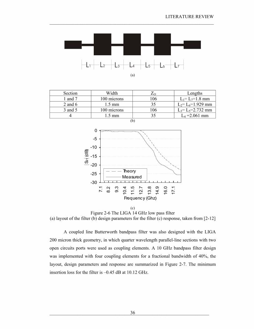
Lowpass and bandpass LIGA microstrip filters with design frequencies of 10
and 14 GHz, were fabricated and the results are summarized as follows. A 14 GHz
stepped impedance low pass filter with 200 micron thick conductors was designed with
a 3 dB cutoff frequency of 13.4 GHz, and an attenuation of 20 dB at 17.1 GHz, the
layout, design parameters and response are summarized in Figure 2-6. The minimum
insertion loss for the filter is –0.15 dB at 8.07 GHz, the filter has a flat response from
7.1 to its corner frequency.
LITERATURE REVIEW ______________________________________________________________________
____________________________________________________________________ 36
(a)
Section Width ZO Lengths 1 and 7 100 microns 106 L1= L7=1.8 mm 2 and 6 1.5 mm 35 L2= L6=1.929 mm 3 and 5 100 microns 106 L3= L5=2.732 mm
4 1.5 mm 35 L4 =2.061 mm (b)
0
-5
-10
-15
-20
-25
-30
7.1
8.2
9.3
10.4
11.5
12.7
13.8
14.9
16.0
17.1
Frequency (Ghz)
S (d
B) 2
1
TheoryMeasured
(c) Figure 2-6 The LIGA 14 GHz low pass filter
(a) layout of the filter (b) design parameters for the filter (c) response, taken from [2-12]
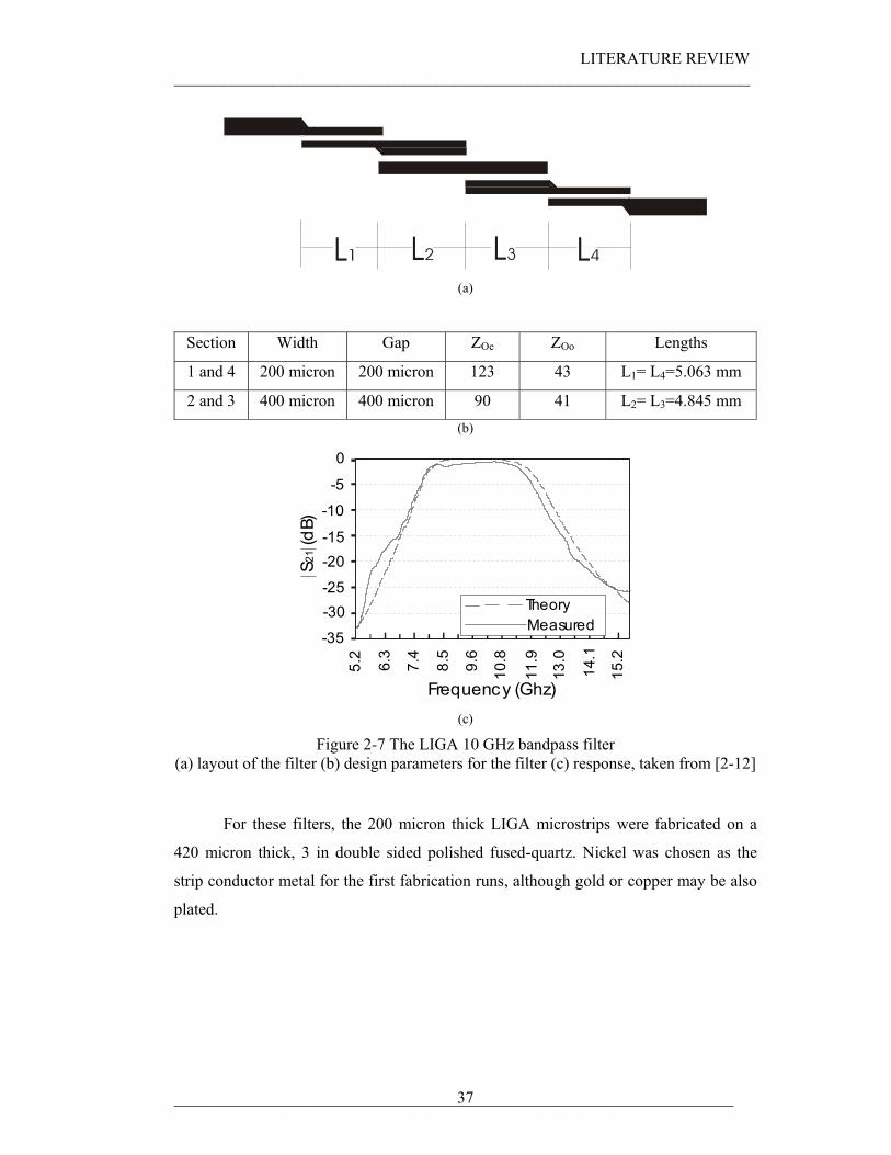
A coupled line Butterworth bandpass filter was also designed with the LIGA
200 micron thick geometry, in which quarter wavelength parallel-line sections with two
open circuits ports were used as coupling elements. A 10 GHz bandpass filter design
was implemented with four coupling elements for a fractional bandwidth of 40%, the
layout, design parameters and response are summarized in Figure 2-7. The minimum
insertion loss for the filter is –0.45 dB at 10.12 GHz.
LITERATURE REVIEW ______________________________________________________________________
____________________________________________________________________ 37
(a)
Section Width Gap ZOe ZOo Lengths
1 and 4 200 micron 200 micron 123 43 L1= L4=5.063 mm
2 and 3 400 micron 400 micron 90 41 L2= L3=4.845 mm (b)
0
-5
-10
-15-20
-25
-35
5.2
Frequency (Ghz)
S (d
B) 2
1
-30
6.3
7.4
8.5
9.6
10.8
11.9
13.0
14.1
15.2
MeasuredTheory
(c)
Figure 2-7 The LIGA 10 GHz bandpass filter (a) layout of the filter (b) design parameters for the filter (c) response, taken from [2-12]
For these filters, the 200 micron thick LIGA microstrips were fabricated on a
420 micron thick, 3 in double sided polished fused-quartz. Nickel was chosen as the
strip conductor metal for the first fabrication runs, although gold or copper may be also
plated.
LITERATURE REVIEW ______________________________________________________________________
____________________________________________________________________ 38
2.4.4 MEMBRANE SUPPORTED FILTERS
Membrane supported striplines [2-13] and microstrips [2-14],[2-15] have
become a way of producing high performance millimetre wave circuits. High
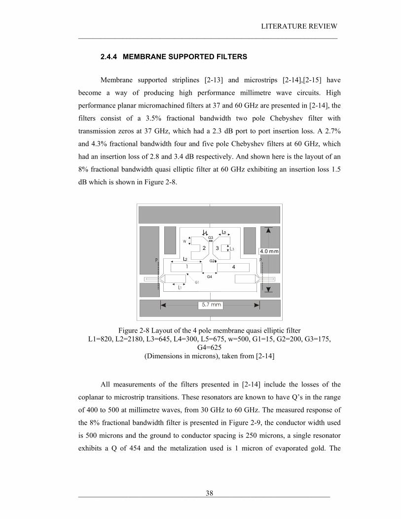
performance planar micromachined filters at 37 and 60 GHz are presented in [2-14], the
filters consist of a 3.5% fractional bandwidth two pole Chebyshev filter with
transmission zeros at 37 GHz, which had a 2.3 dB port to port insertion loss. A 2.7%
and 4.3% fractional bandwidth four and five pole Chebyshev filters at 60 GHz, which
had an insertion loss of 2.8 and 3.4 dB respectively. And shown here is the layout of an
8% fractional bandwidth quasi elliptic filter at 60 GHz exhibiting an insertion loss 1.5
dB which is shown in Figure 2-8.
4.0 mm
4
G4
G2L2
2 3
G3L4 L5
Figure 2-8 Layout of the 4 pole membrane quasi elliptic filter
L1=820, L2=2180, L3=645, L4=300, L5=675, w=500, G1=15, G2=200, G3=175, G4=625
(Dimensions in microns), taken from [2-14]
All measurements of the filters presented in [2-14] include the losses of the
coplanar to microstrip transitions. These resonators are known to have Q’s in the range
of 400 to 500 at millimetre waves, from 30 GHz to 60 GHz. The measured response of
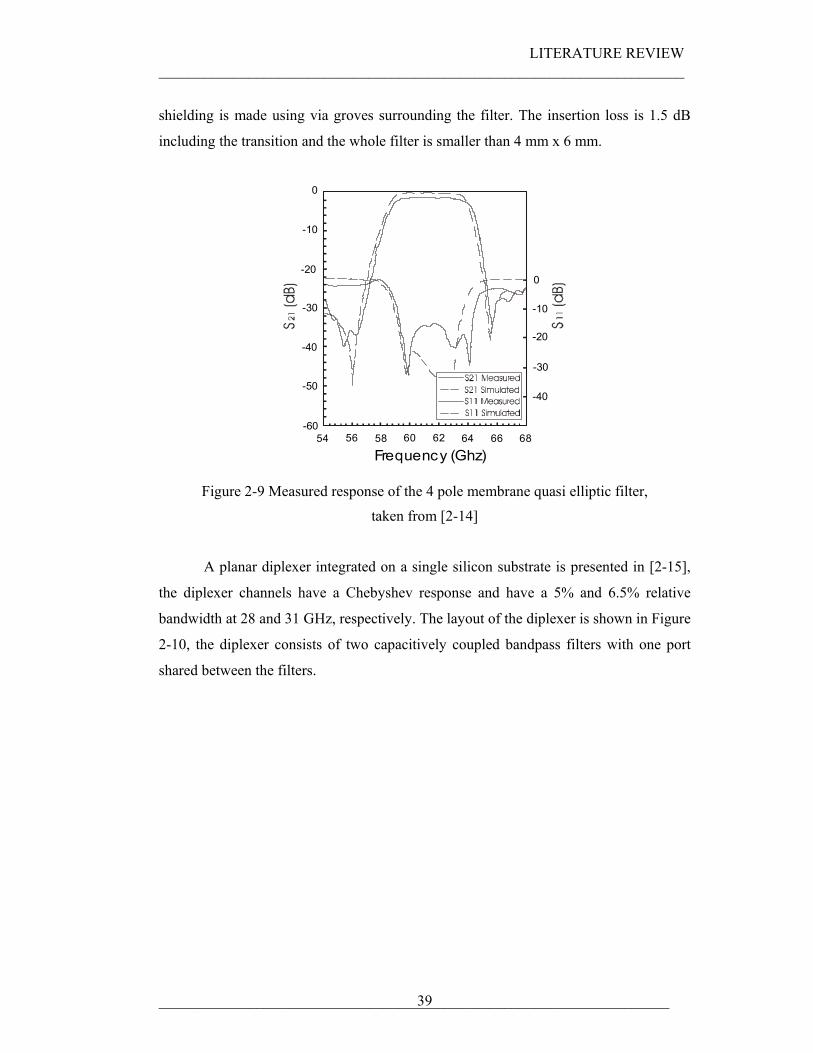
the 8% fractional bandwidth filter is presented in Figure 2-9, the conductor width used
is 500 microns and the ground to conductor spacing is 250 microns, a single resonator
exhibits a Q of 454 and the metalization used is 1 micron of evaporated gold. The
LITERATURE REVIEW ______________________________________________________________________
____________________________________________________________________ 39
shielding is made using via groves surrounding the filter. The insertion loss is 1.5 dB
including the transition and the whole filter is smaller than 4 mm x 6 mm.
Frequency (Ghz)
-60
-50
-40
-30
-20
-10
0
-40
-30
-20
-10
0
54 56 58 60 62 64 66 68
Figure 2-9 Measured response of the 4 pole membrane quasi elliptic filter,
taken from [2-14]
A planar diplexer integrated on a single silicon substrate is presented in [2-15],
the diplexer channels have a Chebyshev response and have a 5% and 6.5% relative
bandwidth at 28 and 31 GHz, respectively. The layout of the diplexer is shown in Figure
2-10, the diplexer consists of two capacitively coupled bandpass filters with one port
shared between the filters.
LITERATURE REVIEW ______________________________________________________________________
____________________________________________________________________ 40
Common Port
TransmitPort
Receive PortResonators
Silicon
Membrane
Via groves
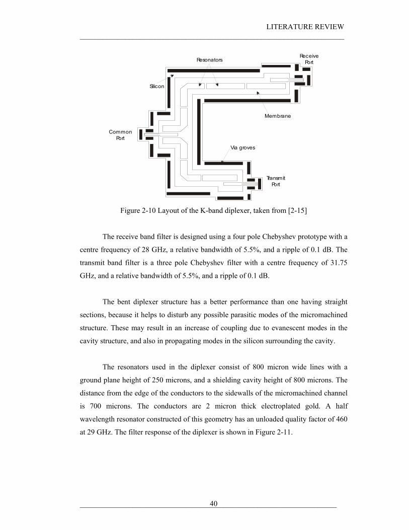
Figure 2-10 Layout of the K-band diplexer, taken from [2-15]
The receive band filter is designed using a four pole Chebyshev prototype with a
centre frequency of 28 GHz, a relative bandwidth of 5.5%, and a ripple of 0.1 dB. The
transmit band filter is a three pole Chebyshev filter with a centre frequency of 31.75
GHz, and a relative bandwidth of 5.5%, and a ripple of 0.1 dB.
The bent diplexer structure has a better performance than one having straight
sections, because it helps to disturb any possible parasitic modes of the micromachined
structure. These may result in an increase of coupling due to evanescent modes in the
cavity structure, and also in propagating modes in the silicon surrounding the cavity.
The resonators used in the diplexer consist of 800 micron wide lines with a
ground plane height of 250 microns, and a shielding cavity height of 800 microns. The
distance from the edge of the conductors to the sidewalls of the micromachined channel
is 700 microns. The conductors are 2 micron thick electroplated gold. A half
wavelength resonator constructed of this geometry has an unloaded quality factor of 460
at 29 GHz. The filter response of the diplexer is shown in Figure 2-11.
LITERATURE REVIEW ______________________________________________________________________
____________________________________________________________________ 41
0
-10
-20
-30
Frequency (Ghz)
Resp
onse
(dB)
-40
-50
-70
-60
22 24 26 28 343230
Transmit PathReceive Path
Filter to Filter IsolationReturn Loss
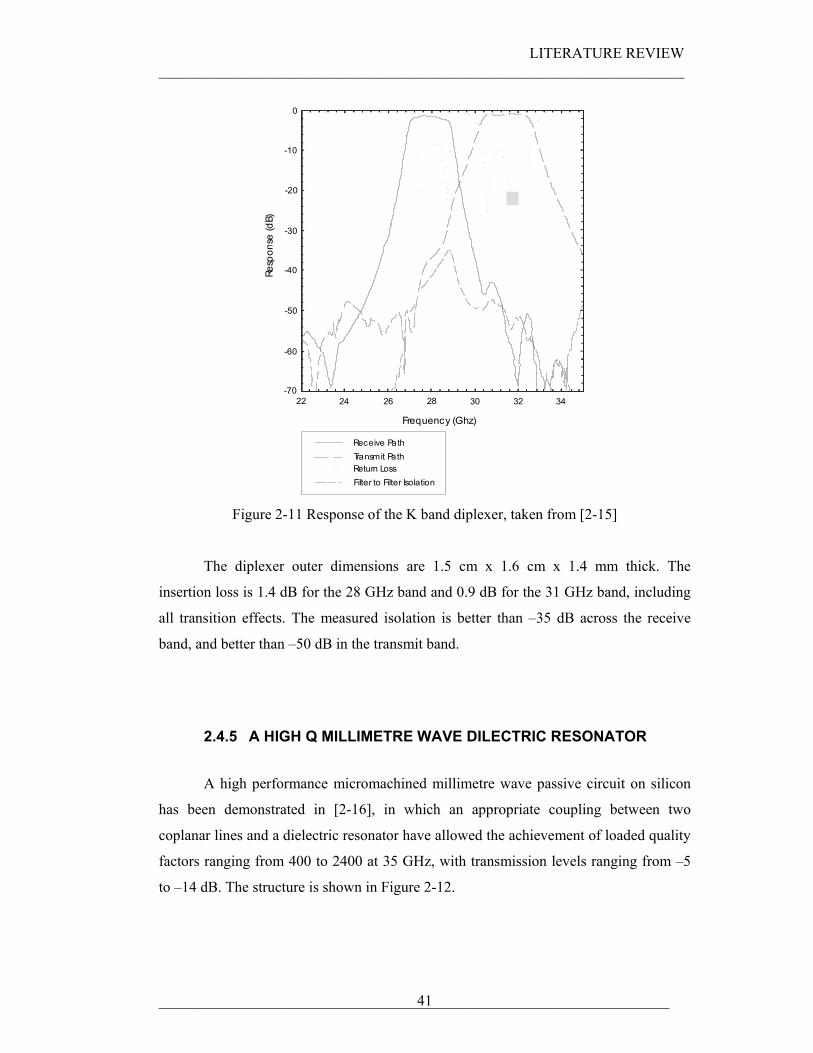
Figure 2-11 Response of the K band diplexer, taken from [2-15]
The diplexer outer dimensions are 1.5 cm x 1.6 cm x 1.4 mm thick. The
insertion loss is 1.4 dB for the 28 GHz band and 0.9 dB for the 31 GHz band, including
all transition effects. The measured isolation is better than –35 dB across the receive
band, and better than –50 dB in the transmit band.
2.4.5 A HIGH Q MILLIMETRE WAVE DILECTRIC RESONATOR
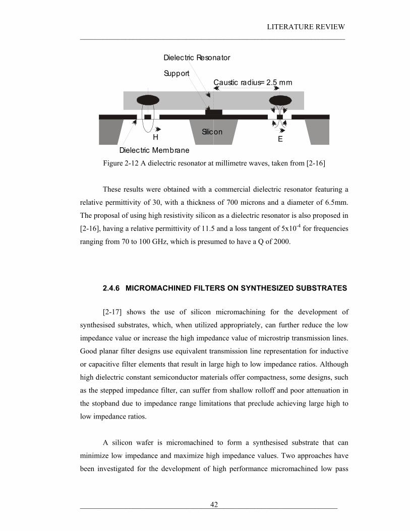
A high performance micromachined millimetre wave passive circuit on silicon
has been demonstrated in [2-16], in which an appropriate coupling between two
coplanar lines and a dielectric resonator have allowed the achievement of loaded quality
factors ranging from 400 to 2400 at 35 GHz, with transmission levels ranging from –5
to –14 dB. The structure is shown in Figure 2-12.
LITERATURE REVIEW ______________________________________________________________________
____________________________________________________________________ 42
Caustic radius= 2.5 mmSupport
Dielectric Resonator
H
Dielectric MembraneE
Silicon
Figure 2-12 A dielectric resonator at millimetre waves, taken from [2-16]
These results were obtained with a commercial dielectric resonator featuring a
relative permittivity of 30, with a thickness of 700 microns and a diameter of 6.5mm.
The proposal of using high resistivity silicon as a dielectric resonator is also proposed in
[2-16], having a relative permittivity of 11.5 and a loss tangent of 5x10⁻⁴ for frequencies
ranging from 70 to 100 GHz, which is presumed to have a Q of 2000.
2.4.6 MICROMACHINED FILTERS ON SYNTHESIZED SUBSTRATES
[2-17] shows the use of silicon micromachining for the development of
synthesised substrates, which, when utilized appropriately, can further reduce the low
impedance value or increase the high impedance value of microstrip transmission lines.
Good planar filter designs use equivalent transmission line representation for inductive
or capacitive filter elements that result in large high to low impedance ratios. Although
high dielectric constant semiconductor materials offer compactness, some designs, such
as the stepped impedance filter, can suffer from shallow rolloff and poor attenuation in
the stopband due to impedance range limitations that preclude achieving large high to
low impedance ratios.
A silicon wafer is micromachined to form a synthesised substrate that can
minimize low impedance and maximize high impedance values. Two approaches have
been investigated for the development of high performance micromachined low pass
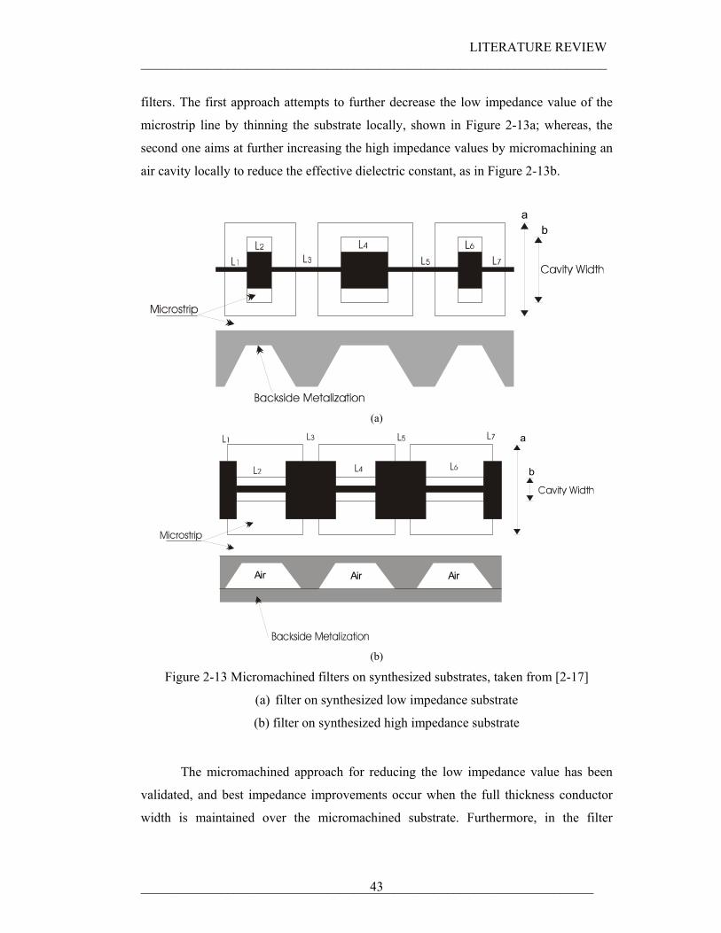
LITERATURE REVIEW ______________________________________________________________________
____________________________________________________________________ 43
filters. The first approach attempts to further decrease the low impedance value of the
microstrip line by thinning the substrate locally, shown in Figure 2-13a; whereas, the
second one aims at further increasing the high impedance values by micromachining an
air cavity locally to reduce the effective dielectric constant, as in Figure 2-13b.
aA
Ab
(a)
aA
Ab
AirAir Air
(b)
Figure 2-13 Micromachined filters on synthesized substrates, taken from [2-17]
(a) filter on synthesized low impedance substrate
(b) filter on synthesized high impedance substrate
The micromachined approach for reducing the low impedance value has been
validated, and best impedance improvements occur when the full thickness conductor
width is maintained over the micromachined substrate. Furthermore, in the filter
LITERATURE REVIEW ______________________________________________________________________
____________________________________________________________________ 44
response, sharper rejection band edges have been achieved for increased high to low
impedance ratios by a factor of 1.5. In the micromachined approach for increasing the
high impedance value, two primary advantages are observed: 1) a reduction in
fabrication and design tolerances, which allow for practical realization, and 2) a
reduction of ohmic losses as a result of wider conducting lines. The measured response
for a seven section Chebyshev synthesized high impedance filter on a 250 micron thick
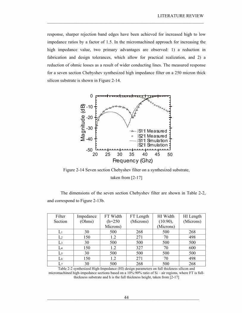
silicon substrate is shown in Figure 2-14.
0
20
-10
-50
-20
-40
-30
Frequency (Ghz)
Mag
nitu
de (d
B)
25 30 35 40 45 50
S11 MeasuredS21 MeasuredS11 Simula tionS21 Simulation
Figure 2-14 Seven section Chebyshev filter on a synthesized substrate,
taken from [2-17]
The dimensions of the seven section Chebyshev filter are shown in Table 2-2,
and correspond to Figure 2-13b.
Filter Section
Impedance (Ohms)
FT Width (h=250
Microns)
FT Length (Microns)
HI Width (10:90),
(Microns)
HI Length (Microns)
L1 30 500 268 500 268 L2 150 1.2 271 70 498 L3 30 500 500 500 500 L4 150 1.2 327 70 600 L5 30 500 500 500 500 L6 150 1.2 271 70 498 L7 30 500 268 500 268 Table 2-2 synthesized High-Impedance (HI) design parameters on full thickness silicon and
micromachined high-impedance sections based on a 10%:90% ratio of Si – air regions, where FT is full-thickness substrate and h is the full thickness height, taken from [2-17]
LITERATURE REVIEW ______________________________________________________________________
____________________________________________________________________ 45
2.4.7 MICROMACHINED TUNABLE FILTERS
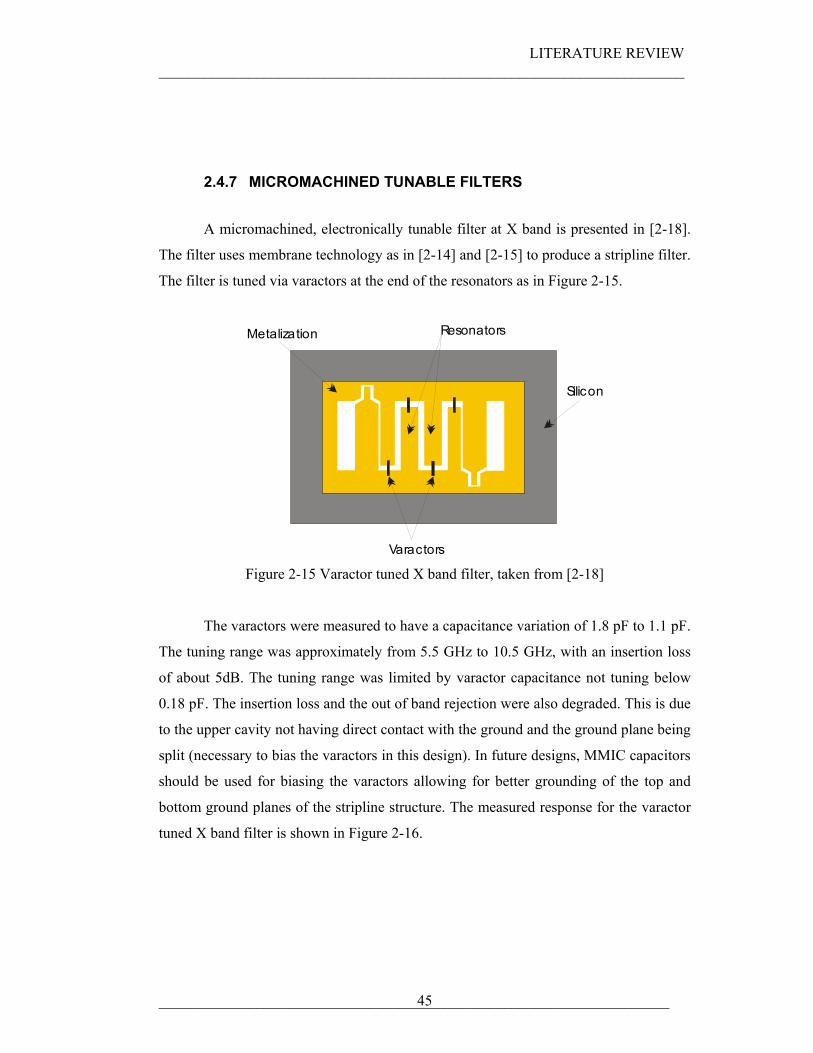
A micromachined, electronically tunable filter at X band is presented in [2-18].
The filter uses membrane technology as in [2-14] and [2-15] to produce a stripline filter.
The filter is tuned via varactors at the end of the resonators as in Figure 2-15.
Resonators
Silicon
Metalization
Varactors Figure 2-15 Varactor tuned X band filter, taken from [2-18]
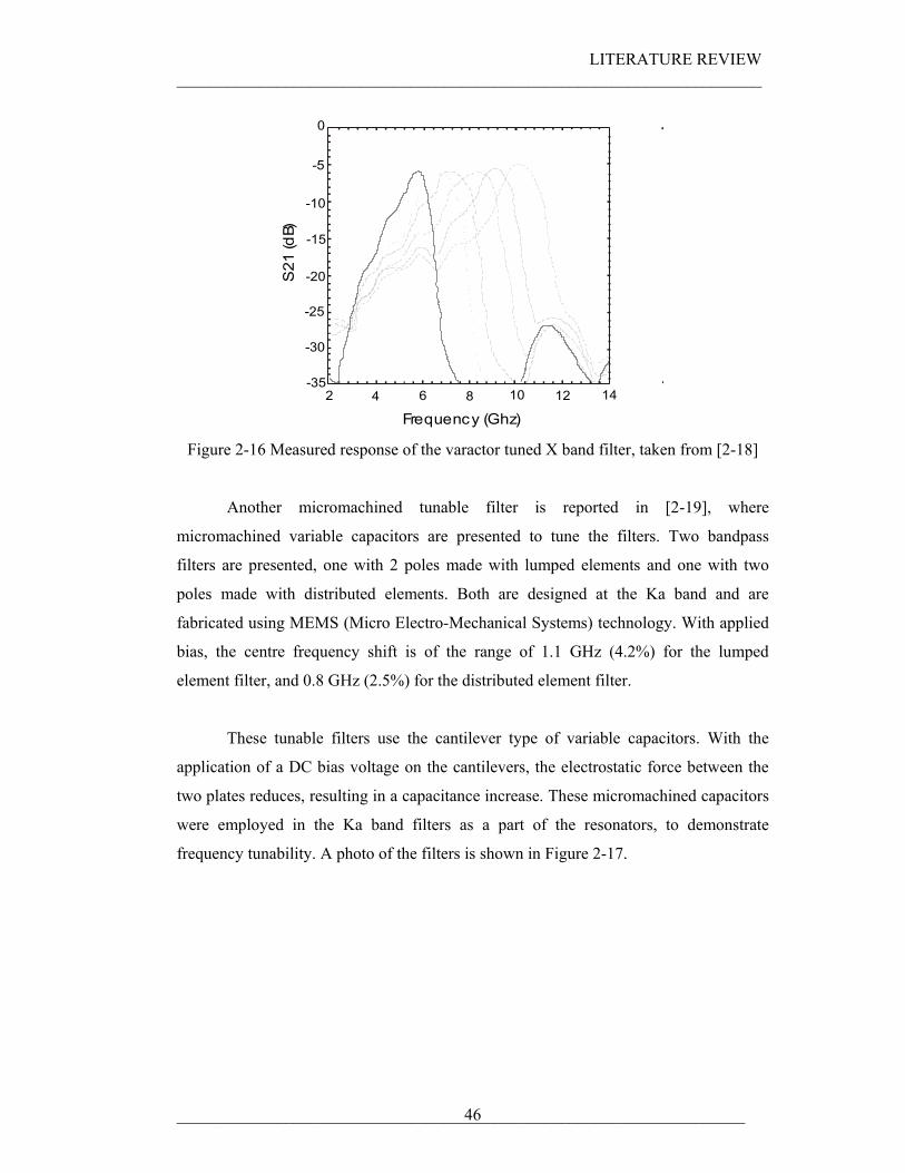
The varactors were measured to have a capacitance variation of 1.8 pF to 1.1 pF.
The tuning range was approximately from 5.5 GHz to 10.5 GHz, with an insertion loss
of about 5dB. The tuning range was limited by varactor capacitance not tuning below
0.18 pF. The insertion loss and the out of band rejection were also degraded. This is due
to the upper cavity not having direct contact with the ground and the ground plane being
split (necessary to bias the varactors in this design). In future designs, MMIC capacitors
should be used for biasing the varactors allowing for better grounding of the top and
bottom ground planes of the stripline structure. The measured response for the varactor
tuned X band filter is shown in Figure 2-16.
LITERATURE REVIEW ______________________________________________________________________
____________________________________________________________________ 46
0
-5
-10
-15
-20
-25
-30
S 21
(dB)
Frequency (Ghz)
-352 6 8 10 12 144
Figure 2-16 Measured response of the varactor tuned X band filter, taken from [2-18]
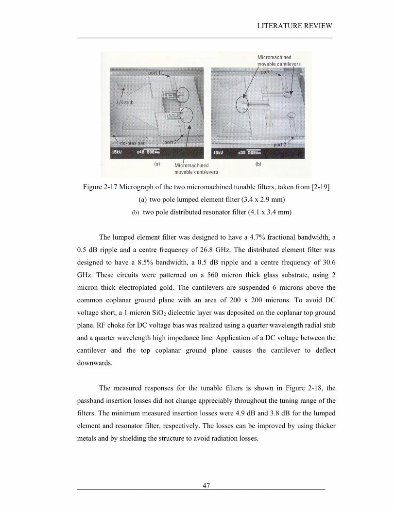
Another micromachined tunable filter is reported in [2-19], where
micromachined variable capacitors are presented to tune the filters. Two bandpass
filters are presented, one with 2 poles made with lumped elements and one with two
poles made with distributed elements. Both are designed at the Ka band and are
fabricated using MEMS (Micro Electro-Mechanical Systems) technology. With applied
bias, the centre frequency shift is of the range of 1.1 GHz (4.2%) for the lumped
element filter, and 0.8 GHz (2.5%) for the distributed element filter.
These tunable filters use the cantilever type of variable capacitors. With the
application of a DC bias voltage on the cantilevers, the electrostatic force between the
two plates reduces, resulting in a capacitance increase. These micromachined capacitors
were employed in the Ka band filters as a part of the resonators, to demonstrate
frequency tunability. A photo of the filters is shown in Figure 2-17.
LITERATURE REVIEW ______________________________________________________________________
____________________________________________________________________ 47
Figure 2-17 Micrograph of the two micromachined tunable filters, taken from [2-19]
(a) two pole lumped element filter (3.4 x 2.9 mm)
(b) two pole distributed resonator filter (4.1 x 3.4 mm)
The lumped element filter was designed to have a 4.7% fractional bandwidth, a
0.5 dB ripple and a centre frequency of 26.8 GHz. The distributed element filter was
designed to have a 8.5% bandwidth, a 0.5 dB ripple and a centre frequency of 30.6
GHz. These circuits were patterned on a 560 micron thick glass substrate, using 2
micron thick electroplated gold. The cantilevers are suspended 6 microns above the
common coplanar ground plane with an area of 200 x 200 microns. To avoid DC
voltage short, a 1 micron SiO2 dielectric layer was deposited on the coplanar top ground
plane. RF choke for DC voltage bias was realized using a quarter wavelength radial stub
and a quarter wavelength high impedance line. Application of a DC voltage between the
cantilever and the top coplanar ground plane causes the cantilever to deflect
downwards.
The measured responses for the tunable filters is shown in Figure 2-18, the
passband insertion losses did not change appreciably throughout the tuning range of the
filters. The minimum measured insertion losses were 4.9 dB and 3.8 dB for the lumped
element and resonator filter, respectively. The losses can be improved by using thicker
metals and by shielding the structure to avoid radiation losses.
LITERATURE REVIEW ______________________________________________________________________
____________________________________________________________________ 48
32
-30
-20
-10
0
Frequency (Ghz)22 24 26 3028
-40
0 V
10
0
-10
-15
5
-5
65 V50 V
(a)
Frequency (Ghz)
-30
-20
-10
0
-40
4015 20 25 30 35 45-50
20
-20
10
-10
0
-30
0 V
50 V
(b)
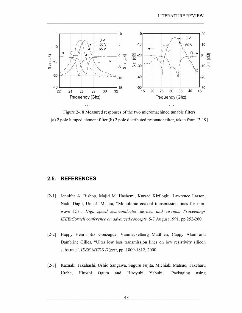
Figure 2-18 Measured responses of the two micromachined tunable filters
(a) 2 pole lumped element filter (b) 2 pole distributed resonator filter, taken from [2-19]
2.5. REFERENCES
[2-1] Jennifer A. Bishop, Majid M. Hashemi, Kursad Kiziloglu, Lawrence Larson,
Nadir Dagli, Umesh Mishra, “Monolithic coaxial transmission lines for mm-
wave ICs”, High speed semiconductor devices and circuits, Proceedings
IEEE/Cornell conference on advanced concepts, 5-7 August 1991, pp 252-260.
[2-2] Happy Henri, Six Gonzague, Vanmackelberg Matthieu, Cappy Alain and
Dambrine Gilles, “Ultra low loss transmission lines on low resistivity silicon
substrate”, IEEE MTT-S Digest, pp. 1809-1812, 2000.
[2-3] Kazuaki Takahashi, Ushio Sangawa, Suguru Fujita, Michiaki Matsuo, Takeharu
Urabe, Hiroshi Ogura and Hiroyuki Yabuki, “Packaging using
LITERATURE REVIEW ______________________________________________________________________
____________________________________________________________________ 49
microelectromechanical technologies and planar components” IEEE
Transactions on microwave theory and techniques, Vol. 49, No. 11, pp. 2099-
2104, November 2001.
[2-4] Jae-Hyoung Park, Chang-Wook Baek, Sanghwa Jung, Hong-Teuk Kim,
Youngwoo Kwon and Yong-Kweon Kim, “Novel micromachined coplanar
waveguide transmission lines for application in millimetre-wave circuits” Jpn. J.
Appl. Phys. Vol. 39, Part 1, No. 12B, pp. 7120-7124, December 2000.
[2-5] Pierre Blondy, Andrew R. Brown, Dominique Cross and Gabriel M. Rebeiz,
“Low loss micromachined filters for millimetre-wave telecommunication
systems” IEEE MTT-S Digest, pp. 1181-1184, 1998.
[2-6] Katherine Juliet Herrick, Thomas A. Schwartz and Linda P. B. Katehi, “Si-
micromachined coplanar waveguides for use in high-frequency circuits” IEEE
Transactions on microwave theory and techniques, Vol. 46, No. 6, pp 762-768,
June 1998.
[2-7] Wai Y. Liu, D. Paul Steenson and Michael B. Steer, “Membrane-supported
CPW with mounted active devices” IEEE Microwave and wireless components
letters, Vol. 11, No. 4, April 2001.
[2-8] J.E. Harriss, L.W. Pearson, X. Wang, C.H. Barron and A.V. Pham, “Membrane-
supported Ka band resonator employing organic micromachined packaging”
IEEE MTT-S Digest, pp. 1225-1228, 2000.
[2-9] W.Y. Liu, D.P. Steenson, M.B. Steer, “Membrane-supported e-plane circuits”,
IEEE MTT-S Digest, pp. 539-542, 2001
[2-10] John Papapolymerou, Jui-Ching Cheng, Jack East and Linda P.B. Katehi, “A
Micromachined High-Q X-band resonator”, IEEE Microwave and guided
letters, Vol 7, No 6, June 1997.
LITERATURE REVIEW ______________________________________________________________________
____________________________________________________________________ 50
[2-11] Lee Harle and Linda P.B. Katehi, “A vertically integrated micromachined
filter”, IEEE transactions on theory and techniques, Vol 50, No 9, September
2002.
[2-12] Theodore L. Willke and Steven S. Gearhart, “LIGA micromachined planar
transmission lines and filters”, IEEE transactions on microwave theory and
techniques, Vol 45, No 10, October 1997.
[2-13] Chen-Yu Chi and Gabriel Rebeiz, “Conductor loss limited stripline resonator
and filters”, IEEE transactions on microwave theory and techniques, Vol 44, No
4, April 1996.
[2-14] Pierre Blondy, Andrew R. Brown, Dominique Cros and Gabriel M. Rebeiz,
“Low loss micromachined filters for millimetre wave communication systems”,
IEEE transactions on microwave theory and techniques, Vol 46, No 12,
December 1998.
[2-15] Andrew R. Brown and Gabriel M. Rebeiz, “A high performance integrated K-
band diplexer”, IEEE transactions on microwave theory and techniques, Vol 47,
No 8, August 1999.
[2-16] B. Guillon, D. Cros, P. Pons, K.Grenier, T. Parra, J.L. Cazaux, J.C. Lalaurie, J.
Graffeuil and R. Plana, “Design and realization of high Q millimetre wave
structures through micromachining techniques”, IEEE MTT-S Digest, pp. 1519-
1522, 1999.
[2-17] Rhonda Franklin Drayton, Sergio Palma Pacheco, Jianei Wang, Jong-Gwan
Yook, Linda P.B. Katehi, “Micromachined filters on synthesized substrates”,
IEEE transactions on microwave theory and techniques, Vol 49, No 2, February
2001.
LITERATURE REVIEW ______________________________________________________________________
____________________________________________________________________ 51
[2-18] Andrew R. Brown and Gabriel M. Rebeiz, “Micromachined micropackaged
filter banks and tunable bandpass filters”, IEEE wireless communications
conference, Proceedings 11-13, August 1997, pp 193-197.
[2-19] Hong-Teuk Kim, Jae-Hyoung Park, Yong-Kweon Kim and Youngwoo Kwon,
“Millimeter wave micromachined tunable filters”, IEEE MTT-S Digest, pp.
1235-1238, 1999.
I.Llamas-Garro, PhD thesis (2003), The University of Birmingham, UK
3. CHAPTER THREE
TRANSMISSION LINE THEORY
3.1 INTRODUCTION
In this Chapter a review of basic transmission line theory will be presented, the
theory used in this Chapter can be found in [3-1] to [3-9]. The first section deals with
the lumped element model of a transmission line, out of which the telegrapher’s
equations will be derived. These equations are general and relate voltages and currents
on the transmission line to any point in time and space.
In section 3.3, standing waves will be introduced by the example of a lossless
transmission line terminated in a mismatched load, which will produce reflected waves
on the transmission line that combine with the generated wave leading to standing
waves. The input impedance of a low loss, half wavelength transmission line terminated
TRANSMISSION LINE THEORY ______________________________________________________________________
____________________________________________________________________ 53
in an open circuit will also be reviewed in this section, this result will be used later in
Chapter 4, section 4.3.
In Section 3.4 wave propagation will be introduced and the wave equations
derived, followed by the definition of the TEM (Transverse Electromagnetic Mode)
mode, also in this section dispersion problems in transmission lines will be addressed.
Finally at the end of the chapter, basic transmission lines used in microwave
engineering will be presented.
3.2 THE TELEGRAPHER EQUATIONS
Microwave transmission lines may differ significantly in physical form, which
leads to different electromagnetic field patterns. The objective of this section will be to
describe the impedance and propagation characteristics of a transmission line; the
method is general, based on ac circuit theory, and it is valid regardless of the
electromagnetic field pattern of the transmission line.
In 1855 the studies made by William Thomson (Lord Kevin) led to the first
distributed circuit analysis of a transmission line. His model consisted of uniformly
distributed series resistances and shunt capacitances. This was the beginning of
transmission line theory. Later on, after the telephone was invented by Bell and Gray in
1876, a more detailed study of transmission lines was carried out by Oliver Heaviside,
his analysis appears practically unaltered in today’s text books.
A transmission line is often schematically represented as a two wire line, since
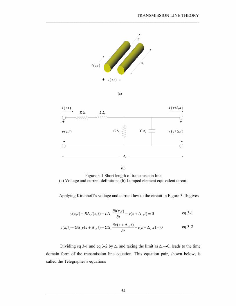
transmission lines for TEM wave propagation always have at least two conductors.
Figure 3-1 represents a short piece of transmission line, where ∆z can always be chosen
to be small compared to the operating wavelength, in the derivation ∆z → 0, and hence
the results are valid at all frequencies.
TRANSMISSION LINE THEORY ______________________________________________________________________
____________________________________________________________________ 54
∆z
z
v ( z,t )
i ( z,t )
+ - (a)
R ∆z L ∆z
C ∆z G ∆z
i ( z,t )
v ( z,t )
i ( z+∆z,t )
v ( z+∆z,t )
∆z
+
-
+
-
(b)
Figure 3-1 Short length of transmission line (a) Voltage and current definitions (b) Lumped element equivalent circuit
Applying Kirchhoff’s voltage and current law to the circuit in Figure 3-1b gives
0),(),(),(),( =∆+−∂
∂∆−∆− tzv
ttziLtziRtzv zzz eq 3-1
0),(),(),(),( =∆+−∂∆+∂
∆−∆+∆− tzit
tzvCtzvGtzi zz
zzz eq 3-2
Dividing eq 3-1 and eq 3-2 by ∆z and taking the limit as ∆z→0, leads to the time
domain form of the transmission line equation. This equation pair, shown below, is
called the Telegrapher’s equations
TRANSMISSION LINE THEORY ______________________________________________________________________
____________________________________________________________________ 55
ttziLtzRi
ztzv
∂∂
−−=∂
∂ ),(),(),( eq 3-3
ttzvCtzGv
ztzi
∂∂
−−=∂
∂ ),(),(),( eq 3-4
The Telegrapher’s equations are general, relating voltages and currents on the
transmission line to any point in time and space, via the line parameters R, L, G and C.
The negative signs indicate that the voltage and current will decrease with an increasing
distance z.
Frequently we are concerned with a single frequency steady state sinusoidal
voltage or current that can be represented by the phasors
tj
oevtv ω=)( eq 3-5
tjoeiti ω=)( eq 3-6
Differentiating these equations results in
)(tvjevjtv tj
o ωω ω ==∂∂
eq 3-7
)(tijeijti tj
o ωω ω ==∂∂ eq 3-8
In this case eq 3-3 and eq 3-4 simplify to
)()()( ziLjRzzv ω+−=
∂∂
eq 3-9
)()()( zvCjGzzi ω+−=
∂∂ eq 3-10
TRANSMISSION LINE THEORY ______________________________________________________________________
____________________________________________________________________ 56
Eliminating i(z) and v(z) from eq 3-9 and eq 3-10 respectively by cross
substitution yields
)()())(()( 22
2
zvzvCjGLjRz
zv γωω =++=∂
∂
eq 3-11
)()())(()( 22
2
ziziCjGLjRz
zi γωω =++=∂∂
eq 3-12
Where
))(( CjGLjRj ωωβαγ ++=+= eq 3-13
In eq 3-13, γ is called the Propagation constant, the real part of γ is called the
attenuation constant represented by α, the units of α are in Np per unit length. The
imaginary part of γ is called the phase constant represented by β, which describes the
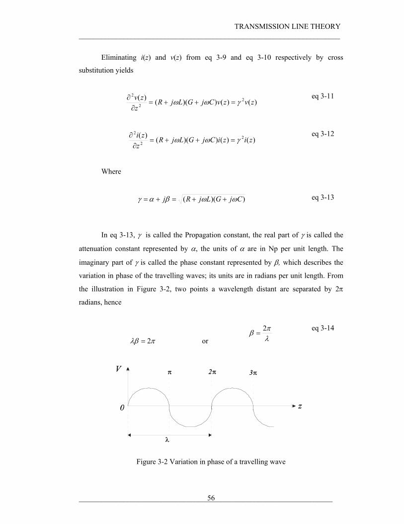
variation in phase of the travelling waves; its units are in radians per unit length. From
the illustration in Figure 3-2, two points a wavelength distant are separated by 2π
radians, hence
πλβ 2= or λπβ 2
= eq 3-14
z 0
V π 2π 3π
λ
Figure 3-2 Variation in phase of a travelling wave
TRANSMISSION LINE THEORY ______________________________________________________________________
____________________________________________________________________ 57
The second order differential equations, eq 3-11 and eq 3-12, are of standard
form and by differentiation and back substitution, the solutions are readily shown to be
zz eVeVzv γγ −−+ += 21)( eq 3-15
zz eIeIzi γγ −−+ += 21)( eq 3-16
Where V1+, V2
-, I1+, I2
- are arbitrary amplitude constants, and the terms with e-γz
represent wave propagation in the +z direction, and the terms with eγz represent wave
propagation in the –z direction. By substitution of eq 3-9 in the voltage of eq 3-15 gives
the current of the line
)()( 21zz eVeV
LjRzi γγ
ωγ −−+ −+
= eq 3-17
Knowing that the characteristic impedance of the line is equal to the ratio of the
voltage to current of the line, when the line is matched, and comparing eq 3-17 with eq
3-16, show that the characteristic impedance of the transmission line is
CjGLjRLjRZo
ωω
γω
++
=+
= eq 3-18
The current on the line is related to the voltage and the characteristic impedance
of the transmission line in the following ways
OZVI
++ = 1
1 eq 3-19
OZVI
−− −= 2
2 eq 3-20
TRANSMISSION LINE THEORY ______________________________________________________________________
____________________________________________________________________ 58
The negative sign in eq 3-20 derives from the fact that the current I2- is travelling
in the negative z direction.
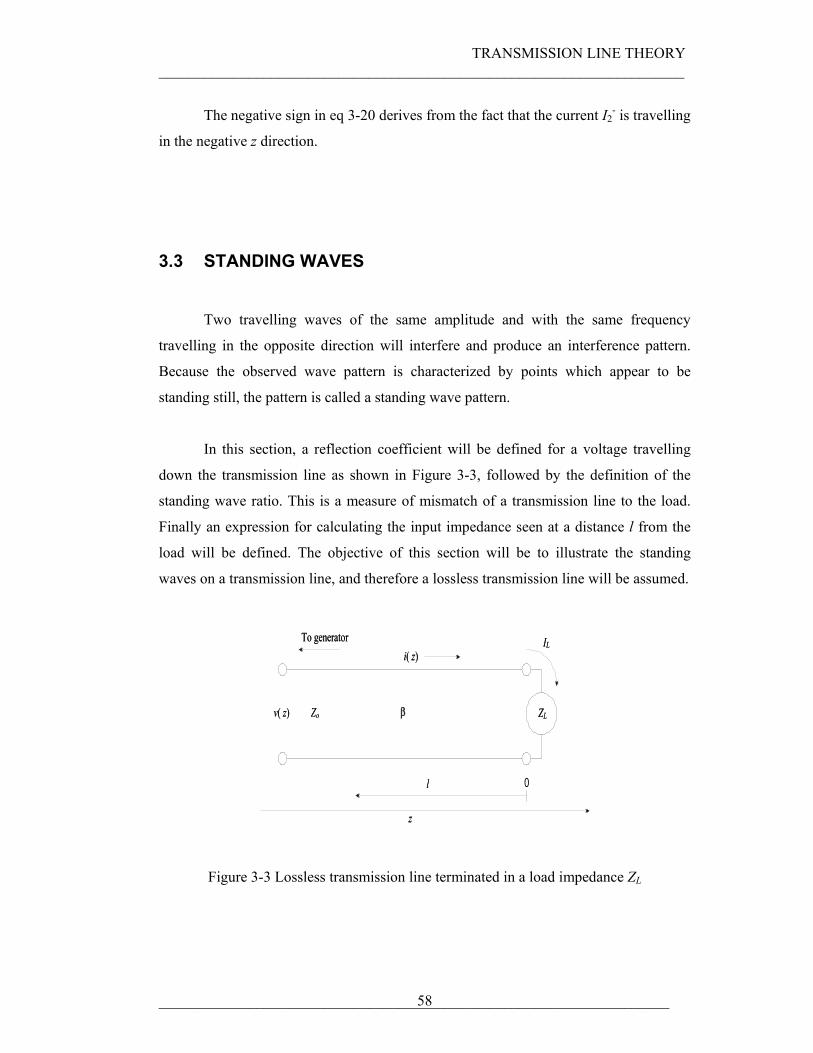
3.3 STANDING WAVES
Two travelling waves of the same amplitude and with the same frequency
travelling in the opposite direction will interfere and produce an interference pattern.
Because the observed wave pattern is characterized by points which appear to be
standing still, the pattern is called a standing wave pattern.
In this section, a reflection coefficient will be defined for a voltage travelling
down the transmission line as shown in Figure 3-3, followed by the definition of the
standing wave ratio. This is a measure of mismatch of a transmission line to the load.
Finally an expression for calculating the input impedance seen at a distance l from the
load will be defined. The objective of this section will be to illustrate the standing
waves on a transmission line, and therefore a lossless transmission line will be assumed.
z
To generator i( z)
v( z)
l
Zo ZL
IL
β
0
Figure 3-3 Lossless transmission line terminated in a load impedance ZL
TRANSMISSION LINE THEORY ______________________________________________________________________
____________________________________________________________________ 59
A travelling wave is generated from a source at z<0, as shown on Figure 3-3.
The wave has the following form
zjeVzv β−+= 1)( eq 3-21
As seen previously, the ratio of the voltage to current for the travelling wave is
the characteristic impedance ZO. If the transmission line is terminated in an arbitrary
load ZL ≠ ZO the ratio of voltage to current at the load must be equal to ZL. Therefore a
reflected wave must be generated at the load with the appropriate amplitude to satisfy
this condition.
The load impedance is related to the total voltage and current in the following
way, using eq 3-19 and eq 3-20, at the load, we find
OL ZVVVV
lilvZ −+
−+
−+
===
=21
21
)0()0(
eq 3-22
Solving for the ratio V2-/V1
+, that is the amplitude of the reflected wave
normalized to the amplitude of the incident wave, defined as the voltage reflection
coefficient Γ
OL
OL
ZZZZ
VV
+−
==Γ +
−
1
2 eq 3-23
A current reflection coefficient can also be defined as the ratio of the reflected
current to the incident current. From eq 3-19 and eq 3-20 we can observe that it will be
equal to the negative of the voltage reflection coefficient. The rest of the section will
deal only with the voltage reflection coefficient.
When a load is mismatched, not all the available power from the generator is
delivered to the load. This loss is referred as the return loss RL in dB, and is defined as
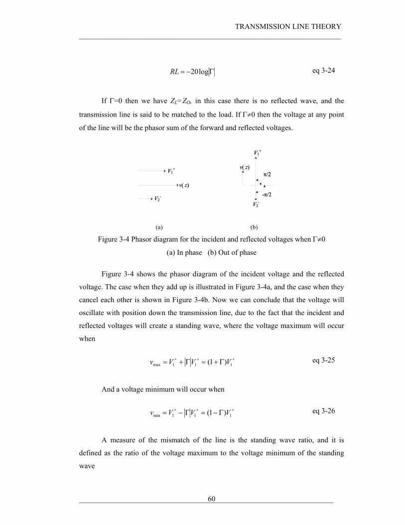
TRANSMISSION LINE THEORY ______________________________________________________________________
____________________________________________________________________ 60
Γ−= log20RL eq 3-24
If Γ=0 then we have ZL=ZO, in this case there is no reflected wave, and the
transmission line is said to be matched to the load. If Γ≠0 then the voltage at any point
of the line will be the phasor sum of the forward and reflected voltages.
v( z)
v( z)V1
+
V1+
V2-
V2-
π/2
-π/2
(a) (b)
Figure 3-4 Phasor diagram for the incident and reflected voltages when Γ≠0
(a) In phase (b) Out of phase
Figure 3-4 shows the phasor diagram of the incident voltage and the reflected
voltage. The case when they add up is illustrated in Figure 3-4a, and the case when they
cancel each other is shown in Figure 3-4b. Now we can conclude that the voltage will
oscillate with position down the transmission line, due to the fact that the incident and
reflected voltages will create a standing wave, where the voltage maximum will occur
when
+++ Γ+=Γ+= 111max )1( VVVv eq 3-25
And a voltage minimum will occur when
+++ Γ−=Γ−= 111min )1( VVVv eq 3-26
A measure of the mismatch of the line is the standing wave ratio, and it is
defined as the ratio of the voltage maximum to the voltage minimum of the standing
wave
TRANSMISSION LINE THEORY ______________________________________________________________________
____________________________________________________________________ 61
Γ−Γ+
==11
min
max
vvSWR
eq 3-27
SWR can take values from 1 to ∞, a SWR=1 implies that the line is matched to
the load.
Taking eq 3-23, that is the refection coefficient at the load, and solving for the
load impedance results in
OL ZZ)1()1(
Γ−Γ+
= eq 3-28
The reflection coefficient can be generalized to any point on the line, with z=-l,
the ratio of the reflected voltage to the incident voltage is
ljlj
lj
eeVeVl β
β
β2
1
2 )0()( −+
−−
Γ==Γ eq 3-29
Where Γ(0) is the reflection coefficient at l=0, now from eq 3-28 and eq 3-29,
the input impedance seen looking toward the load at a distance l=-z from the load is
lj
lj
Oin eeZZ β
β
2
2
11
−
−
Γ−Γ+
= eq 3-30
By using eq 3-23 in eq 3-30 gives
ljOL
ljOL
ljOL
ljOL
Oin eZZeZZeZZeZZZZ ββ
ββ
−
−
−−+−++
=)()()()(
eq 3-31
Using the following Euler’s identities relating trigonometric and exponential
functions
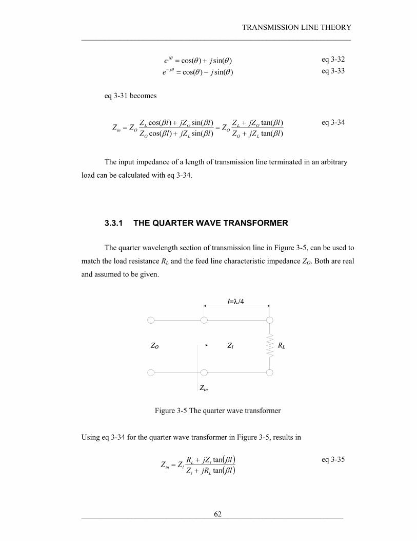
TRANSMISSION LINE THEORY ______________________________________________________________________
____________________________________________________________________ 62
)sin()cos( θθθ je j += eq 3-32
)sin()cos( θθθ je j −=− eq 3-33
eq 3-31 becomes
)tan()tan(
)sin()cos()sin()cos(
ljZZljZZZ
ljZlZljZlZZZ
LO
OLO
LO
OLOin β
βββββ
++
=++
= eq 3-34
The input impedance of a length of transmission line terminated in an arbitrary
load can be calculated with eq 3-34.
3.3.1 THE QUARTER WAVE TRANSFORMER
The quarter wavelength section of transmission line in Figure 3-5, can be used to
match the load resistance RL and the feed line characteristic impedance ZO. Both are real
and assumed to be given.
ZO Zl
Zin
RL
l=λ/4
Figure 3-5 The quarter wave transformer
Using eq 3-34 for the quarter wave transformer in Figure 3-5, results in
( )( )ljRZ
ljZRZZLl
lLlin β
βtantan
++
= eq 3-35
TRANSMISSION LINE THEORY ______________________________________________________________________
____________________________________________________________________ 63
Now by using eq 3-14, we can see that for a quarter wavelength section of
transmission line
2πβ =l eq 3-36
By dividing the numerator and denominator in eq 3-35 by tan(βl), and taking the
limit as βl→π/2, results in
L
lin R
ZZ2
= eq 3-37
From eq 3-37 we can see that a quarter wavelength section of a transmission line
has the effect of transforming the load impedance in an inverse manner. In order to have
no reflections, we must have Zin=ZO, so the characteristic impedance of the quarter
wavelength section of transmission line is given by
LOl RZZ = eq 3-38
This condition applies only when the length of the matching line is λ/4 long, or
an odd multiple (2n+1) of λ/4. Note that this condition can be reached at one frequency,
and a mismatch will occur at other frequencies.
3.3.2 A HALFWAVELENGTH TRANSMISSION LINE TERMINATED IN AN OPEN CIRCUIT
For a transmission line, the voltage and current on the transmission line, can be
written as
TRANSMISSION LINE THEORY ______________________________________________________________________
____________________________________________________________________ 64
( ) [ ]zzo eeVzv γγ Γ+= −+ eq 3-39
( ) [ ]zz
O
o eeZVzi γγ Γ−= −
+
eq 3-40
Where Vo+ is the amplitude of the voltage of an incident wave generated from a
source, similar to eq 3-21. If the transmission line is terminated in an open circuit, such
that ZL=∞, from eq 3-23, we find that the reflection coefficient for this case is Γ=1, and
from eq 3-27 we find that the standing wave ratio is SWR=∞, and the input impedance
of the line is given by
( )( )li
lvZin −−
= eq 3-41
Now by substituting eq 3-39 and eq 3-40 into eq 3-41, results in
[ ]ll
llO
in eeeeZZ γγ
γγ
−
−
Γ−Γ+
= eq 3-42
Using the following identity
( ) θθ
θθ
θ −
−
−+
=eeeecoth
eq 3-43
The input impedance in eq 3-42, for Γ=1, reduces to
lZZ Oin γcoth= eq 3-44
Note that eq 3-44 includes losses in the transmission line, since it contains the
propagation constant γ, while eq 3-34 is valid for a lossless case.
TRANSMISSION LINE THEORY ______________________________________________________________________
____________________________________________________________________ 65
3.4 WAVE PROPAGATION
This section deals with important characteristics of plane wave propagation; the
result will be used later in Chapter 4, section 4.4.1, where conductor loss is discussed.
The first section deals with the wave equations; in the second section the transverse
electromagnetic wave propagation will be discussed, followed by a description of
dispersion. Related to this are the phase and group velocities of the signals that travel
through a transmission line, which concludes the section.
3.4.1 THE WAVE EQUATION
In this section the wave equation that governs the propagation of
electromagnetic waves will be derived, the objective will be to derive the propagation
constant and the general formulation for a wave from an electromagnetic point of view.
This contrasts with the propagation constant in eq 3-13, which was derived from a
lumped element model. For this purpose we will consider a linear, isotropic and
homogeneous medium, where we will assume that the net free charge in the region is
zero, so ρ=0. Any currents in the region are conduction currents σE, in the medium
ED ε= eq 3-45
HB µ= eq 3-46
EJ σ= eq 3-47
Where D is the electric flux density, E is the electric field intensity, B is the
magnetic flux density, H is the magnetic field intensity, ε is the permittivity and µ is
the permeability. Maxwell’s equations in point form for this region become
tHE∂∂
−=×∇ µ eq 3-48
TRANSMISSION LINE THEORY ______________________________________________________________________
____________________________________________________________________ 66
tEEH∂∂
+=×∇ εσ eq 3-49
0=⋅∇ E eq 3-50
0=⋅∇ H eq 3-51
Taking the curl of eq 3-48 and substituting into eq 3-49, results in
2
2
tE
tEE
∂∂
−∂∂
−=×∇×∇ µεµσ eq 3-52
Similarly, by taking the curl of eq 3-49 and substituting into eq 3-48, results in
2
2
tH
tHH
∂∂
−∂∂
−=×∇×∇ µεµσ eq 3-53
In order to interpret these results the following vector identity will be used
( ) AAA 2∇−⋅∇∇=×∇×∇ eq 3-54
Now, substituting eq 3-54 into eq 3-52 and eq 3-53 gives the wave equations,
namely
2
22
tE
tEE
∂∂
+∂∂
=∇ µεµσ eq 3-55
2
22
tH
tHH
∂∂
+∂∂
=∇ µεµσ eq 3-56
Now considering a sinusoidal steady state variation of the field vectors, the wave
equations become
( ) ( ) EjEjE ˆˆˆ 22 ωµεωµσ +=∇ eq 3-57
TRANSMISSION LINE THEORY ______________________________________________________________________
____________________________________________________________________ 67
( ) ( ) HjHjH ˆˆˆ 22 ωµεωµσ +=∇ eq 3-58
Rearranging terms
( )EjjE ˆˆ2 ωεσωµ +=∇ eq 3-59
( )HjjH ˆˆ2 ωεσωµ +=∇ eq 3-60
Where
( )ωεσωµγ jj +=2 eq 3-61
The positive square root of γ 2 is referred as the propagation constant of the
medium given by
βαγ j+= eq 3-62
( )ωεσωµγ jj += eq 3-63
The propagation constant in eq 3-63 describes the propagation characteristics of
an electromagnetic field, in contrast to the propagation constant in eq 3-13, which
describes the propagation characteristics of a voltage or a current.
The general equations of a wave in terms of the phasor field vectors eq 3-59 and
eq 3-60, can be expanded in terms of components. These will be useful for the
derivation of the surface resistance in chapter 4 section 4.4.1, since
2
2
2
2
2
22
ˆˆˆˆzE
yE
xEE xxx
x ∂∂
+∂∂
+∂∂
=∇ eq 3-64
Resulting in
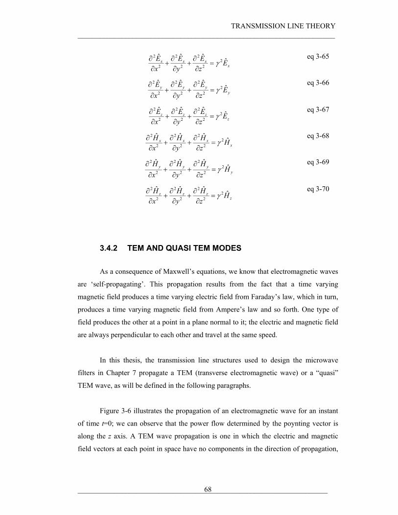
TRANSMISSION LINE THEORY ______________________________________________________________________
____________________________________________________________________ 68
xxxx E
zE
yE
xE ˆˆˆˆ
22
2
2
2
2
2
γ=∂∂
+∂∂
+∂∂
eq 3-65
yyyy E
zE
yE
xE ˆ
ˆˆˆ2
2
2
2
2
2
2
γ=∂∂
+∂∂
+∂∂
eq 3-66
zzzz E
zE
yE
xE ˆˆˆˆ
22
2
2
2
2
2
γ=∂∂
+∂∂
+∂∂
eq 3-67
xxxx H
zH
yH
xH ˆˆˆˆ
22
2
2
2
2
2
γ=∂∂
+∂∂
+∂∂
eq 3-68
yyyy H
zH
yH
xH ˆ
ˆˆˆ2
2
2
2
2
2
2
γ=∂∂
+∂∂
+∂∂
eq 3-69
zzzz H
zH
yH
xH ˆˆˆˆ
22
2
2
2
2
2
γ=∂∂
+∂∂
+∂∂
eq 3-70
3.4.2 TEM AND QUASI TEM MODES
As a consequence of Maxwell’s equations, we know that electromagnetic waves
are ‘self-propagating’. This propagation results from the fact that a time varying
magnetic field produces a time varying electric field from Faraday’s law, which in turn,
produces a time varying magnetic field from Ampere’s law and so forth. One type of
field produces the other at a point in a plane normal to it; the electric and magnetic field
are always perpendicular to each other and travel at the same speed.
In this thesis, the transmission line structures used to design the microwave
filters in Chapter 7 propagate a TEM (transverse electromagnetic wave) or a “quasi”
TEM wave, as will be defined in the following paragraphs.
Figure 3-6 illustrates the propagation of an electromagnetic wave for an instant
of time t=0; we can observe that the power flow determined by the poynting vector is
along the z axis. A TEM wave propagation is one in which the electric and magnetic
field vectors at each point in space have no components in the direction of propagation,
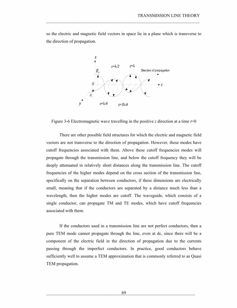
TRANSMISSION LINE THEORY ______________________________________________________________________
____________________________________________________________________ 69
so the electric and magnetic field vectors in space lie in a plane which is transverse to
the direction of propagation.
z
x
y
0
z=λ/4
z=λ/2
z=3λ/4
z=λ Ex
H y
Direction of propagation
Figure 3-6 Electromagnetic wave travelling in the positive z direction at a time t=0
There are other possible field structures for which the electric and magnetic field
vectors are not transverse to the direction of propagation. However, these modes have
cutoff frequencies associated with them. Above these cutoff frequencies modes will
propagate through the transmission line, and below the cutoff frequency they will be
deeply attenuated in relatively short distances along the transmission line. The cutoff
frequencies of the higher modes depend on the cross section of the transmission line,
specifically on the separation between conductors, if these dimensions are electrically
small, meaning that if the conductors are separated by a distance much less than a
wavelength, then the higher modes are cutoff. The waveguide, which consists of a
single conductor, can propagate TM and TE modes, which have cutoff frequencies
associated with them.
If the conductors used in a transmission line are not perfect conductors, then a
pure TEM mode cannot propagate through the line, even at dc, since there will be a
component of the electric field in the direction of propagation due to the currents
passing through the imperfect conductors. In practice, good conductors behave
sufficiently well to assume a TEM approximation that is commonly referred to as Quasi
TEM propagation.
TRANSMISSION LINE THEORY ______________________________________________________________________
____________________________________________________________________ 70
The phase velocity Vp, that is the velocity at which a fixed phase point on the
wave in Figure 3-6 travels, is related to the propagation constant by
βω
=pV eq 3-71
3.4.3 DISPERSION
Phase velocity is defined as the velocity of a point of constant phase down the
transmission line, while group velocity is defined as the velocity at which a group of
frequencies travels down the transmission line. Group velocity can be defined as
βω
ddVg =
eq 3-72
Since most communication systems carry information in groups of frequencies,
in base band or radio frequency, it will be of extreme importance that all the frequencies
arrive at the receiving point as a delayed version of the input signal. This implies that all
components of the signal spectrum must be transmitted with the same phase velocity.
This is not always the case; when the phase and group velocities are a function of
frequency, the transmission line is said to be dispersive, as it will disperse or spread a
signal in time. How severe this effect is will depend on the range of velocities, and the
length of the transmission line.
An example of a dispersive transmission line is the rectangular waveguide. The
square coaxial transmission lines used in Chapter 7 are designed to operate in the pure
TEM mode, so they are dispersionless, which is one advantage over the waveguide.
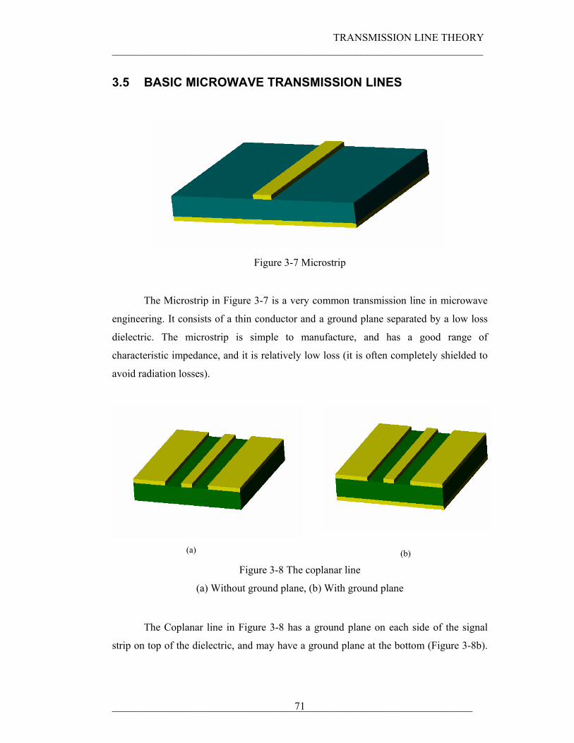
TRANSMISSION LINE THEORY ______________________________________________________________________
____________________________________________________________________ 71
3.5 BASIC MICROWAVE TRANSMISSION LINES
Figure 3-7 Microstrip
The Microstrip in Figure 3-7 is a very common transmission line in microwave
engineering. It consists of a thin conductor and a ground plane separated by a low loss
dielectric. The microstrip is simple to manufacture, and has a good range of
characteristic impedance, and it is relatively low loss (it is often completely shielded to
avoid radiation losses).
(a)
(b)
Figure 3-8 The coplanar line
(a) Without ground plane, (b) With ground plane
The Coplanar line in Figure 3-8 has a ground plane on each side of the signal
strip on top of the dielectric, and may have a ground plane at the bottom (Figure 3-8b).
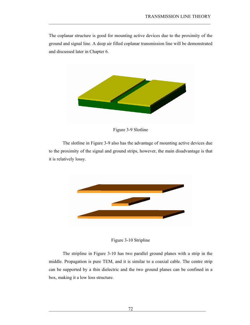
TRANSMISSION LINE THEORY ______________________________________________________________________
____________________________________________________________________ 72
The coplanar structure is good for mounting active devices due to the proximity of the
ground and signal line. A deep air filled coplanar transmission line will be demonstrated
and discussed later in Chapter 6.
Figure 3-9 Slotline
The slotline in Figure 3-9 also has the advantage of mounting active devices due
to the proximity of the signal and ground strips, however, the main disadvantage is that
it is relatively lossy.
Figure 3-10 Stripline
The stripline in Figure 3-10 has two parallel ground planes with a strip in the
middle. Propagation is pure TEM, and it is similar to a coaxial cable. The centre strip
can be supported by a thin dielectric and the two ground planes can be confined in a
box, making it a low loss structure.
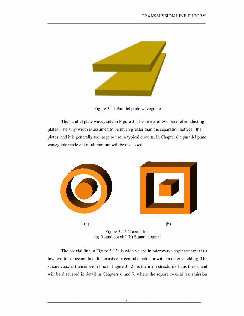
TRANSMISSION LINE THEORY ______________________________________________________________________
____________________________________________________________________ 73
Figure 3-11 Parallel plate waveguide
The parallel plate waveguide in Figure 3-11 consists of two parallel conducting
plates. The strip width is assumed to be much greater than the separation between the
plates, and it is generally too large to use in typical circuits. In Chapter 6 a parallel plate
waveguide made out of aluminium will be discussed.
(a)
(b)
Figure 3-12 Coaxial line (a) Round coaxial (b) Square coaxial
The coaxial line in Figure 3-12a is widely used in microwave engineering; it is a
low loss transmission line. It consists of a central conductor with an outer shielding. The
square coaxial transmission line in Figure 3-12b is the main structure of this thesis, and
will be discussed in detail in Chapters 6 and 7, where the square coaxial transmission
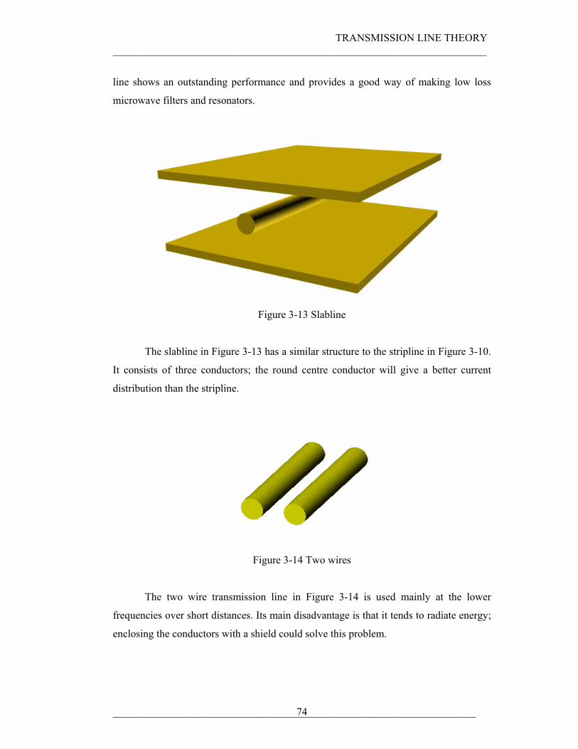
TRANSMISSION LINE THEORY ______________________________________________________________________
____________________________________________________________________ 74
line shows an outstanding performance and provides a good way of making low loss
microwave filters and resonators.
Figure 3-13 Slabline
The slabline in Figure 3-13 has a similar structure to the stripline in Figure 3-10.
It consists of three conductors; the round centre conductor will give a better current
distribution than the stripline.
Figure 3-14 Two wires
The two wire transmission line in Figure 3-14 is used mainly at the lower
frequencies over short distances. Its main disadvantage is that it tends to radiate energy;
enclosing the conductors with a shield could solve this problem.
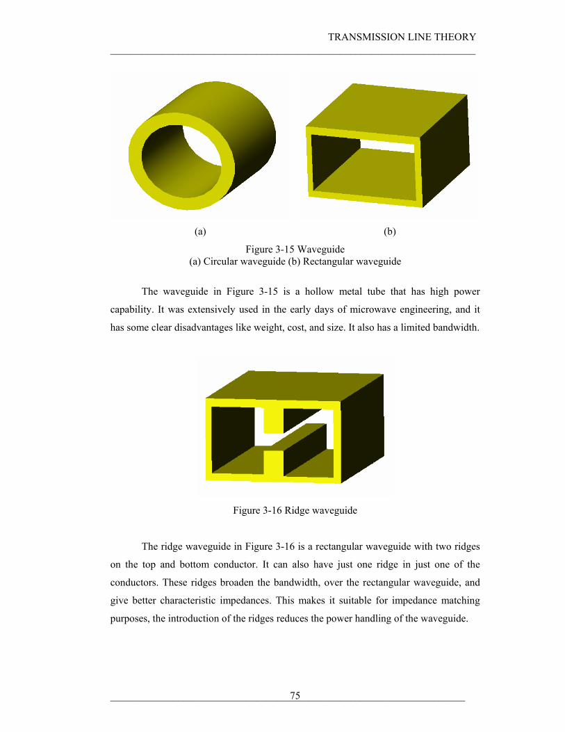
TRANSMISSION LINE THEORY ______________________________________________________________________
____________________________________________________________________ 75
(a)
(b)
Figure 3-15 Waveguide (a) Circular waveguide (b) Rectangular waveguide
The waveguide in Figure 3-15 is a hollow metal tube that has high power
capability. It was extensively used in the early days of microwave engineering, and it
has some clear disadvantages like weight, cost, and size. It also has a limited bandwidth.
Figure 3-16 Ridge waveguide
The ridge waveguide in Figure 3-16 is a rectangular waveguide with two ridges
on the top and bottom conductor. It can also have just one ridge in just one of the
conductors. These ridges broaden the bandwidth, over the rectangular waveguide, and
give better characteristic impedances. This makes it suitable for impedance matching
purposes, the introduction of the ridges reduces the power handling of the waveguide.
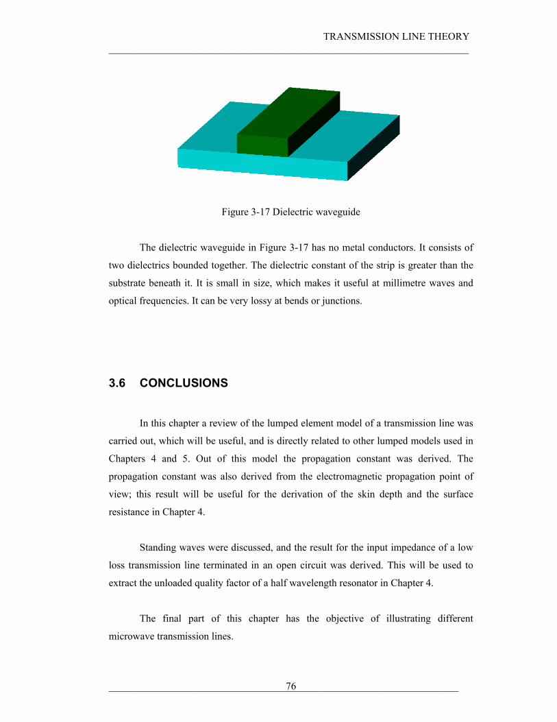
TRANSMISSION LINE THEORY ______________________________________________________________________
____________________________________________________________________ 76
Figure 3-17 Dielectric waveguide
The dielectric waveguide in Figure 3-17 has no metal conductors. It consists of
two dielectrics bounded together. The dielectric constant of the strip is greater than the
substrate beneath it. It is small in size, which makes it useful at millimetre waves and
optical frequencies. It can be very lossy at bends or junctions.
3.6 CONCLUSIONS
In this chapter a review of the lumped element model of a transmission line was
carried out, which will be useful, and is directly related to other lumped models used in
Chapters 4 and 5. Out of this model the propagation constant was derived. The
propagation constant was also derived from the electromagnetic propagation point of
view; this result will be useful for the derivation of the skin depth and the surface
resistance in Chapter 4.
Standing waves were discussed, and the result for the input impedance of a low
loss transmission line terminated in an open circuit was derived. This will be used to
extract the unloaded quality factor of a half wavelength resonator in Chapter 4.
The final part of this chapter has the objective of illustrating different
microwave transmission lines.
TRANSMISSION LINE THEORY ______________________________________________________________________
____________________________________________________________________ 77
3.7 REFERENCES
[3-1] C.W. Davidson, “Transmission lines for communications”, MacMillan
Education Ltd, 1992
[3-2] D.M. Pozar, “Microwave engineering”, John Wiley and Sons Inc., 1998
[3-3] D.M.Pozar, “Microwave and RF design of wireless systems”, John Wiley and
Sons Inc., 2001
[3-4] C.R. Paul et al. “Introduction to electromagnetic fields”, McGraw Hill Co.1998
[3-5] P.A. Rizzi, “Microwave engineering passive circuits”, Prentice Hall Inc. 1988
[3-6] K.F. Sander & G.A.L. Reed, “Transmission and propagation of electromagnetic
waves”, Cambridge University Press, 1986
[3-7] J.C. Slater, “Microwave transmission”, McGraw Hill Co., 1942
[3-8] S.R. Pennock & P.R. Shepherd, “Microwave engineering with wireless
applications”, MacMillan Press Ltd, 1998
[3-9] F.R. Connor, “Waves”, Edward Arnold, 1992
I.Llamas-Garro, PhD thesis (2003), The University of Birmingham, UK
4. CHAPTER FOUR
MICROWAVE RESONATORS
4.1. INTRODUCTION
In this chapter, resonator theory is reviewed; the theory used in this chapter can
be found in references [3-2] to [3-5], [3-8] and from [4-1] to [4-9]. In section 4.2
lumped element resonant circuits are analysed, since the operation of microwave
distributed element resonators can be explained with the help of these circuits. In
section 4.3 the unloaded quality factor for a half wavelength distributed element
resonator will be derived. In section 4.4 material losses will be considered, especially
the conductor loss, since the main structures of this thesis are conductor loss limited
transmission lines. In section 4.5 a practical way of extracting the unloaded quality
factor directly from experimental measurements is presented. Finally, in section 4.6 the
unloaded quality factor for different square coaxial cross sections will be presented, as
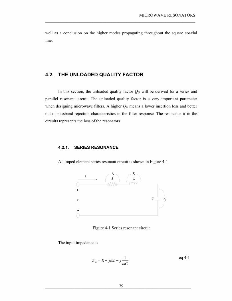
MICROWAVE RESONATORS ______________________________________________________________________
____________________________________________________________________ 79
well as a conclusion on the higher modes propagating throughout the square coaxial
line.
4.2. THE UNLOADED QUALITY FACTOR
In this section, the unloaded quality factor QO will be derived for a series and
parallel resonant circuit. The unloaded quality factor is a very important parameter
when designing microwave filters. A higher QO means a lower insertion loss and better
out of passband rejection characteristics in the filter response. The resistance R in the
circuits represents the loss of the resonators.
4.2.1. SERIES RESONANCE
A lumped element series resonant circuit is shown in Figure 4-1
V
R L
C
I
VC
VR VL
+
-
Figure 4-1 Series resonant circuit
The input impedance is
CjLjRZin ω
ω 1−+= eq 4-1
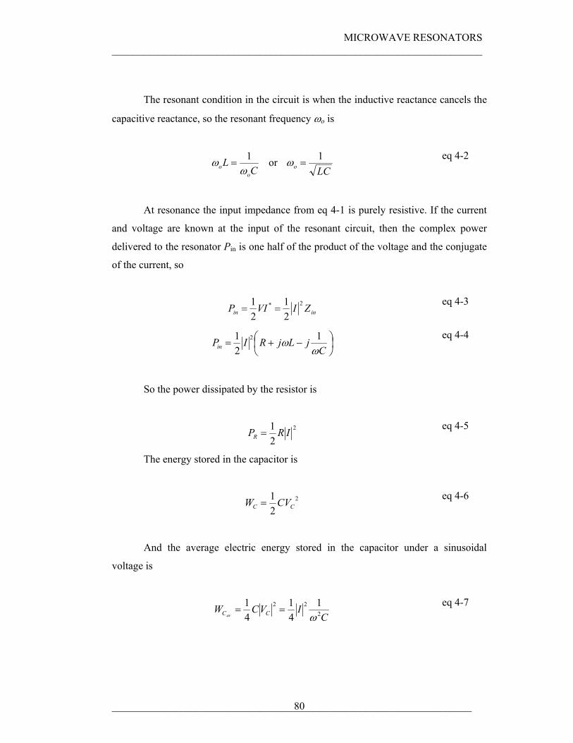
MICROWAVE RESONATORS ______________________________________________________________________
____________________________________________________________________ 80
The resonant condition in the circuit is when the inductive reactance cancels the
capacitive reactance, so the resonant frequency ωo is
CL
oo ω
ω 1= or
LCo1
=ω eq 4-2
At resonance the input impedance from eq 4-1 is purely resistive. If the current
and voltage are known at the input of the resonant circuit, then the complex power
delivered to the resonator Pin is one half of the product of the voltage and the conjugate
of the current, so
inin ZIVIP 2*
21
21
== eq 4-3
⎟⎠⎞
⎜⎝⎛ −+=
CjLjRIPin ω
ω 121 2
eq 4-4
So the power dissipated by the resistor is
2
21 IRPR =
eq 4-5
The energy stored in the capacitor is
2
21
CC CVW = eq 4-6
And the average electric energy stored in the capacitor under a sinusoidal
voltage is
CIVCW CCav 2
22 141
41
ω==
eq 4-7
MICROWAVE RESONATORS ______________________________________________________________________
____________________________________________________________________ 81
The energy stored in the inductor is
2
21 LIWL =
eq 4-8
And the average magnetic energy stored in the inductor under a sinusoidal
current is
2
41 ILW
avL = eq 4-9
The unloaded quality factor for the resonant circuit, is defined as the ratio of the
energy stored in the resonant circuit to the power loss in the resonant circuit at the
resonant frequency, such that
R
LcoO P
WWQ avav
+=ω
eq 4-10
We can obtain the unloaded quality factor for the series resonant circuit, and as
WC=WL at resonance eq 4-10 becomes
RCRLQ
o
oO ω
ω 1== eq 4-11
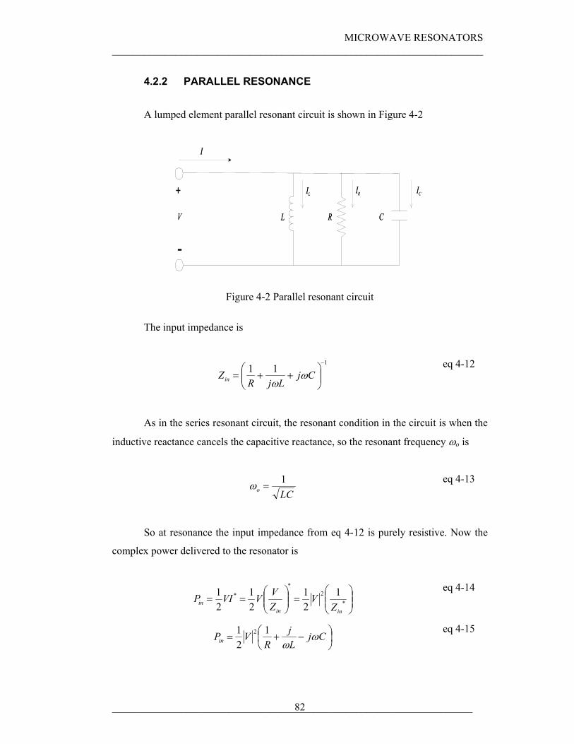
MICROWAVE RESONATORS ______________________________________________________________________
____________________________________________________________________ 82
4.2.2 PARALLEL RESONANCE
A lumped element parallel resonant circuit is shown in Figure 4-2
V R L C
I
IL IR IC +
-
Figure 4-2 Parallel resonant circuit
The input impedance is
1
11−
⎟⎟⎠
⎞⎜⎜⎝
⎛++= Cj
LjRZin ω
ω
eq 4-12
As in the series resonant circuit, the resonant condition in the circuit is when the
inductive reactance cancels the capacitive reactance, so the resonant frequency ωo is
LCo1
=ω eq 4-13
So at resonance the input impedance from eq 4-12 is purely resistive. Now the
complex power delivered to the resonator is
⎟⎟⎠
⎞⎜⎜⎝
⎛=⎟⎟
⎠
⎞⎜⎜⎝
⎛== *
2*
* 121
21
21
ininin Z
VZVVVIP
eq 4-14
⎟⎠⎞
⎜⎝⎛ −+= Cj
Lj
RVPin ω
ω1
21 2
eq 4-15
MICROWAVE RESONATORS ______________________________________________________________________
____________________________________________________________________ 83
So the power dissipated by the resistor is
RV
PR
2
21
= eq 4-16
The average electric energy stored in the capacitor is
CVWavC
2
41
= eq 4-17
And the average magnetic energy stored in the inductor is
LVLIW LLav 2
22 141
41
ω==
eq 4-18
From eq 4-10 we can find the unloaded quality factor for the parallel resonant
circuit, remembering that WC=WL at resonance yields
RCL
RQ oo
O ωω
== eq 4-19
4.3. UNLOADED QUALITY FACTOR OF A HALF WAVELENGTH TRANSMSISSION LINE RESONATOR
By using the input impedance for an open circuited line eq 3-44, and the
following identity
( )θφφθφθ
tanhtan1tantanhtanh
jjj
++
=+ eq 4-20
MICROWAVE RESONATORS ______________________________________________________________________
____________________________________________________________________ 84
The input impedance for an open circuited line of length l can be written as
ljllljZZ Oin βα
αβtantanh
tanhtan1+
+= eq 4-21
Considering ω near resonance
ωωω ∆+= o eq 4-22
Where ∆ω is small. Using eq 3-70 and eq 4-22, results in
pp
o
Vl
Vll ωωβ ∆+= eq 4-23
The length of a half wavelength transmission line resonator for ω=ωo can be
written as
o
pVl
ωπλ
==2
eq 4-24
This result can be verified by substituting eq 3-14 and eq 3-70 into eq 4-24.
Substituting eq 4-24 into eq 4-23, results in
o
lωωππβ ∆
+= eq 4-25
Now
ooo
lωωπ
ωωπ
ωωππβ ∆
≈∆
=⎟⎟⎠
⎞⎜⎜⎝
⎛ ∆+= tantantan
eq 4-26
MICROWAVE RESONATORS ______________________________________________________________________
____________________________________________________________________ 85
The transmission line is assumed to have a small loss such that αl<<1, so
ll αα ≈tanh eq 4-27
By substituting eq 4-26 and eq 4-27 into eq 4-21 results in
o
oOin
jl
ljZZ
ωωπα
αωωπ
∆+
∆+
=1
eq 4-28
The second term in the numerator is small, namely
lo
αωωπ∆
<<1 eq 4-29
So the input impedance can be found by
o
Oin
jl
ZZ
ωωπα ∆
+≈ eq 4-30
Now the input impedance for a parallel resonant circuit eq 4-12 will be
compared to the input impedance of a half wavelength transmission line resonator eq
4-30, for this, near resonance eq 4-12 can be rewritten using the result that [3-2]
...11
1+−≈
+x
x eq 4-31
Now using eq 4-22 and eq 4-13, the input impedance for the parallel resonant
circuit eq 4-12 results in [4-5]
MICROWAVE RESONATORS ______________________________________________________________________
____________________________________________________________________ 86
1
11
−
⎟⎟⎟⎟
⎠
⎞
⎜⎜⎜⎜
⎝
⎛
∆++
∆−
+≈ CjCjLjR
Z oo
oin ωω
ωωω
eq 4-32
1
21
−
⎟⎟⎠
⎞⎜⎜⎝
⎛∆+
∆+≈ Cj
Lj
RZ
oin ω
ωω
eq 4-33
1
21 −
⎟⎠⎞
⎜⎝⎛ ∆+≈ Cj
RZin ω
eq 4-34
RCjRZin ω∆+
≈21
eq 4-35
By comparing eq 4-30 and eq 4-35, the resistance of the equivalent RLC circuit
for the half wavelength resonator is given by
lZR O
α= eq 4-36
Similarly the capacitance of the equivalent RLC circuit for the half wavelength
resonator is
OoZC
ωπ
2= eq 4-37
And the inductance of the equivalent RLC circuit for the half wavelength
resonator is
CL
o21
ω= eq 4-38
Finally the unloaded quality factor for the half wavelength transmission line
resonator can be calculated by using eq 4-19 and eq 4-37
MICROWAVE RESONATORS ______________________________________________________________________
____________________________________________________________________ 87
αβ
απω
22===
lRCQ oO eq 4-39
4.4. MATERIAL LOSSES
In this section, the losses due to the materials used to form transmission line
resonators will be presented.
Ampere’s law for sinusoidal signals in the lossless dielectric case (σ =0), can be
written as
EjH ˆˆ ωε=×∇ eq 4-40
If we include losses, σ≠ 0, the expression can be written as
( )EjH ˆˆ ωεσ +=×∇ eq 4-41
EjjH ˆ1ˆ ⎟⎠⎞
⎜⎝⎛ −=×∇
ωεσωε
eq 4-42
Comparing Ampere’s law for both cases, we can see that the losses can be
included into the lossless case by replacing ε with a complex permittivity given by
⎟⎠⎞
⎜⎝⎛ −=
ωεσεε j1ˆ
eq 4-43
Where the term in the right hand side of the parenthesis is referred as the loss
tangent of the material, namely
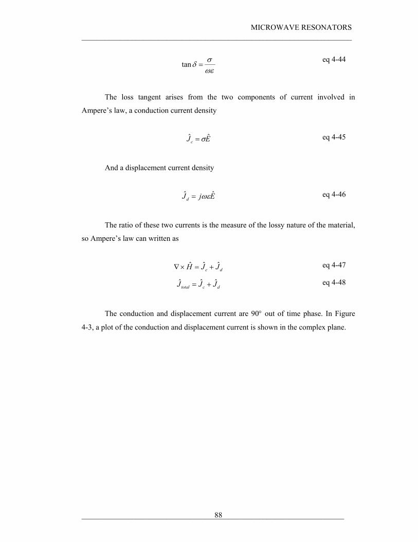
MICROWAVE RESONATORS ______________________________________________________________________
____________________________________________________________________ 88
ωεσδ =tan eq 4-44
The loss tangent arises from the two components of current involved in
Ampere’s law, a conduction current density
EJcˆˆ σ= eq 4-45
And a displacement current density
EjJdˆˆ ωε= eq 4-46
The ratio of these two currents is the measure of the lossy nature of the material,
so Ampere’s law can written as
dc JJH ˆˆˆ +=×∇ eq 4-47
dctotal JJJ ˆˆˆ += eq 4-48
The conduction and displacement current are 90° out of time phase. In Figure
4-3, a plot of the conduction and displacement current is shown in the complex plane.
MICROWAVE RESONATORS ______________________________________________________________________
____________________________________________________________________ 89
totalJ
EJcˆˆ σ=
EJ dˆˆ ωε=
δ
totalJ
EJcˆˆ σ=
EJ dˆˆ ωε=
Figure 4-3 Loss tangent
The loss tangent is related to the conduction current density and the
displacement current density from Figure 4-3 as
ωεσδ ==
d
c
J
Jˆ
ˆtan
eq 4-49
Materials can be classified according to whether the conduction current is much
larger than the displacement current, which corresponds to a good conductor eq 4-50, or
whether the displacement current is much larger than the conduction current, which
corresponds to a good dielectric eq 4-51.
ωεσ
>>1 good conductor eq 4-50
ωεσ
<<1 good dielectric eq 4-51
The expressions of the attenuation constant due to dielectrics are a function of
the loss tangent of the material.
MICROWAVE RESONATORS ______________________________________________________________________
____________________________________________________________________ 90
4.4.1 CONDUCTOR LOSS
Rearranging terms from the propagation constant eq 3-62, we obtain
⎟⎠⎞
⎜⎝⎛ +=
σωεωµσγ jj 1
eq 4-52
Since for a good conductor we have the condition stated in eq 4-50, the
propagation constant for a good conductor becomes
o45∠=≈ ωµσωµσγ j eq 4-53
So that
2ωµσβα ≈=
eq 4-54
The electric field for a forward travelling wave can be written as
( ) xz
m azteEE βωα −= − cos eq 4-55
Where Em is the magnitude of the field, and ax. is the unit vector in the x
direction in Figure 4-4. As the wave travels through the material, its amplitude will be
attenuated by the factor e-αz, now the skin depth δ is the distance over which the current
density falls to 1/e or 37% of its initial value, so
αδ 1
=s eq 4-56
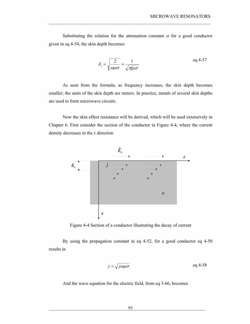
MICROWAVE RESONATORS ______________________________________________________________________
____________________________________________________________________ 91
Substituting the relation for the attenuation constant α for a good conductor
given in eq 4-54, the skin depth becomes
µσπωµσδ
fs12
== eq 4-57
As seen from the formula, as frequency increases, the skin depth becomes
smaller; the units of the skin depth are meters. In practice, metals of several skin depths
are used to form microwave circuits.
Now the skin effect resistance will be derived, which will be used extensively in
Chapter 6. First consider the section of the conductor in Figure 4-4, where the current
density decreases in the x direction
oE
J
σ
x
z
sδ
oE
Js
Figure 4-4 Section of a conductor illustrating the decay of current
By using the propagation constant in eq 4-52, for a good conductor eq 4-50
results in
ωµσγ j= eq 4-58
And the wave equation for the electric field, from eq 3-66, becomes
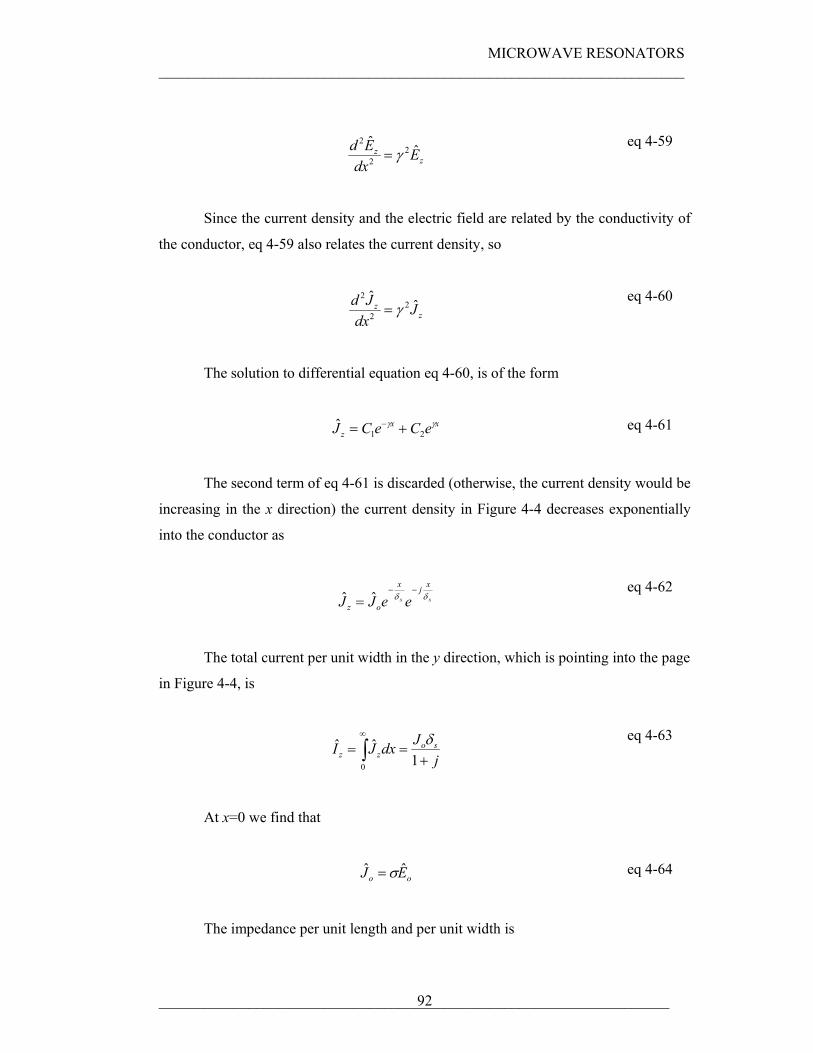
MICROWAVE RESONATORS ______________________________________________________________________
____________________________________________________________________ 92
zz E
dxEd ˆˆ
22
2
γ= eq 4-59
Since the current density and the electric field are related by the conductivity of
the conductor, eq 4-59 also relates the current density, so
zz J
dxJd ˆˆ
22
2
γ= eq 4-60
The solution to differential equation eq 4-60, is of the form
xx
z eCeCJ γγ21
ˆ += − eq 4-61
The second term of eq 4-61 is discarded (otherwise, the current density would be
increasing in the x direction) the current density in Figure 4-4 decreases exponentially
into the conductor as
ss
xjx
oz eeJJ δδ−−
= ˆˆ eq 4-62
The total current per unit width in the y direction, which is pointing into the page
in Figure 4-4, is
∫∞
+==
0 1ˆˆ
jJdxJI so
zzδ
eq 4-63
At x=0 we find that
oo EJ ˆˆ σ= eq 4-64
The impedance per unit length and per unit width is
MICROWAVE RESONATORS ______________________________________________________________________
____________________________________________________________________ 93
z
os I
EZ ˆˆˆ =
eq 4-65
By substituting eq 4-63 and eq 4-64 into eq 4-65, we obtain
ss
jZσδ+
=1ˆ eq 4-66
Where the units of Zs are in Ohms, now we define the impedance as
iss LjRZ ω+=ˆ eq 4-67
From eq 4-66 and eq 4-67, it is possible to identify the slab’s resistance and its
internal inductance per unit width and length as
ssR
σδ1
= eq 4-68
siL
σδω 1
= eq 4-69
So the block of conducting material in Figure 4-4, that has infinite depth in the x
direction and a surface area of 1m2, will have the impedance of eq 4-68 and eq 4-69,
with units of Ohms per square.
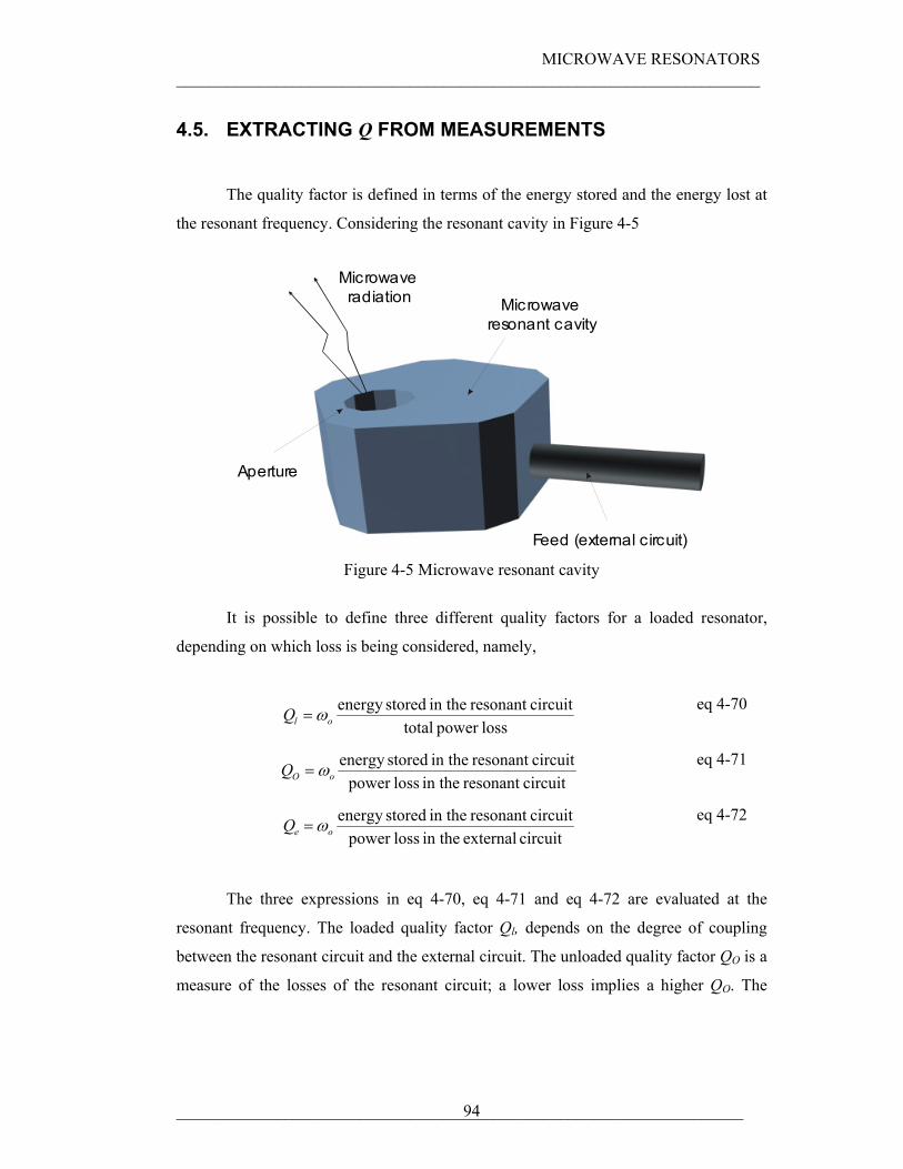
MICROWAVE RESONATORS ______________________________________________________________________
____________________________________________________________________ 94
4.5. EXTRACTING Q FROM MEASUREMENTS
The quality factor is defined in terms of the energy stored and the energy lost at
the resonant frequency. Considering the resonant cavity in Figure 4-5
Microwaveresonant cavity
Feed (external circuit)
Aperture
Microwave radiation
Figure 4-5 Microwave resonant cavity
It is possible to define three different quality factors for a loaded resonator,
depending on which loss is being considered, namely,
losspower totalcircuitresonant in the storedenergy
olQ ω= eq 4-70
circuitresonant in the losspower circuitresonant in the storedenergy
oOQ ω= eq 4-71
circuit external in the losspower circuitresonant in the storedenergy
oeQ ω= eq 4-72
The three expressions in eq 4-70, eq 4-71 and eq 4-72 are evaluated at the
resonant frequency. The loaded quality factor Ql, depends on the degree of coupling
between the resonant circuit and the external circuit. The unloaded quality factor QO is a
measure of the losses of the resonant circuit; a lower loss implies a higher QO. The
MICROWAVE RESONATORS ______________________________________________________________________
____________________________________________________________________ 95
external quality factor Qe is related to the degree to which the resonant circuit is coupled
to the external circuits. The three quality factors are related in the following way
Oel QQQ111
+= eq 4-73
When designing a transmission line resonator, some power may not be available
in the load, which was not caused by material losses, or an impedance mismatch at the
ports of the device. This power may be lost as a result of radiation losses. These losses
mainly depend on the physical structure of the transmission line. When the transmission
line uses semiconductors, leakage losses must be taken into account. Leakage losses are
normally present in dielectrics having finite resistivity, such as the case of
semiconductors.
The losses present in the resonant circuit can be conductor losses Qc, dielectric
losses Qd, radiation losses Qr, or leakage losses Qk. The unloaded quality factor for a
resonant circuit can be calculated by adding these losses, resulting in
krdcO QQQQQ11111
+++= eq 4-74
Next, a practical method to extract the unloaded quality factor from the
measurements of a loaded resonator will be described [4-6] [4-7]. First, consider a
symmetrically loaded resonator. The resonator’s typical transmission response is shown
in Figure 4-6
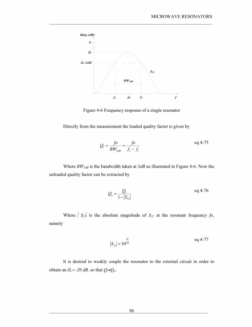
MICROWAVE RESONATORS ______________________________________________________________________
____________________________________________________________________ 96
IL-3dB
IL
Mag (dB)
0
S21
f1 fo f2 f
BW3dB
Figure 4-6 Frequency response of a single resonator
Directly from the measurement the loaded quality factor is given by
123 fffo
BWfoQ
dBl −
== eq 4-75
Where BW3dB is the bandwidth taken at 3dB as illustrated in Figure 4-6. Now the
unloaded quality factor can be extracted by
211 SQQ l
o −= eq 4-76
Where S21is the absolute magnitude of S21 at the resonant frequency fo,
namely
2021 10
IL
S = eq 4-77
It is desired to weakly couple the resonator to the external circuit in order to
obtain an IL> -20 dB, so that Ql≈Qo.
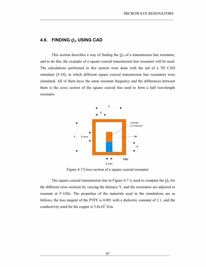
MICROWAVE RESONATORS ______________________________________________________________________
____________________________________________________________________ 97
4.6. FINDING QO USING CAD
This section describes a way of finding the QO of a transmission line resonator,
and to do this, the example of a square coaxial transmission line resonator will be used.
The calculations performed in this section were done with the aid of a 3D CAD
simulator [4-10], in which different square coaxial transmission line resonators were
simulated. All of them have the same resonant frequency and the differences between
them is the cross section of the square coaxial line used to form a half wavelength
resonator.
Air
2 mm
5 mm
PTFE
X
X
Y
Y
Figure 4-7 Cross section of a square coaxial resonator
The square coaxial transmission line in Figure 4-7 is used to compute the QO for
the different cross sections by varying the distance Y, and the resonators are adjusted to
resonate at 9 GHz. The properties of the materials used in the simulations are as
follows, the loss tangent of the PTFE is 0.001 with a dielectric constant of 2.1, and the
conductivity used for the copper is 5.8x10⁷ S/m.
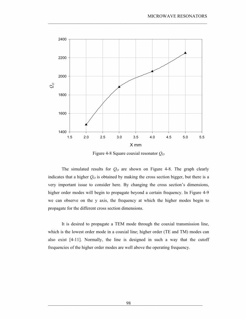
MICROWAVE RESONATORS ______________________________________________________________________
____________________________________________________________________ 98
X mm
1.5 2.0 2.5 3.0 3.5 4.0 4.5 5.0 5.5
QO
1400
1600
1800
2000
2200
2400
Figure 4-8 Square coaxial resonator QO
The simulated results for QO are shown on Figure 4-8. The graph clearly
indicates that a higher QO is obtained by making the cross section bigger, but there is a
very important issue to consider here. By changing the cross section’s dimensions,
higher order modes will begin to propagate beyond a certain frequency. In Figure 4-9
we can observe on the y axis, the frequency at which the higher modes begin to
propagate for the different cross section dimensions.
It is desired to propagate a TEM mode through the coaxial transmission line,
which is the lowest order mode in a coaxial line; higher order (TE and TM) modes can
also exist [4-11]. Normally, the line is designed in such a way that the cutoff
frequencies of the higher order modes are well above the operating frequency.
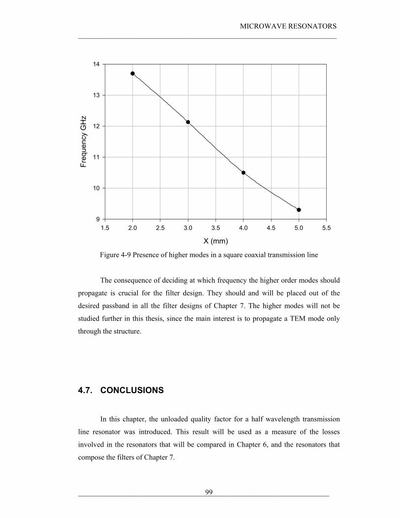
MICROWAVE RESONATORS ______________________________________________________________________
____________________________________________________________________ 99
X (mm)
1.5 2.0 2.5 3.0 3.5 4.0 4.5 5.0 5.5
Freq
uenc
y G
Hz
9
10
11
12
13
14
Figure 4-9 Presence of higher modes in a square coaxial transmission line
The consequence of deciding at which frequency the higher order modes should
propagate is crucial for the filter design. They should and will be placed out of the
desired passband in all the filter designs of Chapter 7. The higher modes will not be
studied further in this thesis, since the main interest is to propagate a TEM mode only
through the structure.
4.7. CONCLUSIONS
In this chapter, the unloaded quality factor for a half wavelength transmission
line resonator was introduced. This result will be used as a measure of the losses
involved in the resonators that will be compared in Chapter 6, and the resonators that
compose the filters of Chapter 7.
MICROWAVE RESONATORS ______________________________________________________________________
____________________________________________________________________ 100
The lumped element resonant circuits presented in this chapter will be
extensively used in the filter theory of Chapter 5, as well as to make calculations of the
losses directly from the measured responses of the filters of Chapter 7, although this
procedure will be further explained in Chapter 5.
Material losses were also introduced in this chapter. The surface resistance will
be used to make the analytical calculations of the attenuation constant due to conductor
loss, and the unloaded quality factor for different half wavelength resonators will be
described and compared in Chapter 6.
The way of extracting the unloaded quality factor from measurements, will be
the method used to make calculations of the different fabricated resonators presented in
Chapter 6.
Finally the unloaded quality factor for a square coaxial transmission line was
presented, including a discussion on higher modes in coaxial lines.
4.8. REFERENCES
[4-1] M.J. Lancaster, “Passive microwave device applications of high temperature
superconductors”, Cambridge University press, 1996
[4-2] S. Ramo, J.R. Whinnery and T.Van Duzer, “Fields and waves in communication
electronics”, John Wiley and Sons Inc, 1984
[4-3] J.W. Nilsson, “Electric circuits”, Addison-Wesley publishing company, 1990
MICROWAVE RESONATORS ______________________________________________________________________
____________________________________________________________________ 101
[4-4] J. Carr and J. Davies “Radio and RF engineer’s pocket handbook”, Newnes an
imprint of Butterworth-Heinemann, 2000
[4-5] R.E. Collin, “Foundations for microwave engineering”, Mc Graw Hill, 1992
[4-6] G. Matthaei, L. Young and E.M.T. Jones, “Microwave filters, impedance
matching networks and coupling structures”, Artech house Inc, 1964
[4-7] Jia-Sheng Hong and M.J. Lancaster, “Microstrip filters for RF/Microwave
applications”, John Wiley and Sons Inc, 2001
[4-8] M. Makimoto and S. Yamashita, “Microwave resonators and filters for wireless
communication”, Springer-Verlag Berlin Heidelberg, 2001
[4-9] H.A. Wheeler, “Formulas for the skin effect”, Proc. IRE., Vol. 30, pp. 412-424,
September 1942
[4-10] Agilent HFSS V 5.5
[3-2] Pozar
[4-11] L. Gruner, “Higher order modes in square coaxial lines”, IEEE transactions on
microwave theory and techniques, Vol. 31, No 9, September 1983.

I.Llamas-Garro, PhD thesis (2003), The University of Birmingham, UK
5. CHAPTER FIVE
GENERAL FILTER DESIGN
5.1. INTRODUCTION
This chapter contains the theory used to design the filters presented in Chapter 7.
These filters have a Chebyshev response. The design procedure for each filter will be
shown individually in Chapter 7. The theory used in this Chapter can be found in [4-6]
to [4-8].
Section 5.2 contains a discussion of the low pass filter prototype, which will be
converted to give a bandpass response in section 5.3; where narrowband coupled
resonator filters will be addressed. The rest of section 5.3 contains the theory on how to
develop a Chebyschev bandpass filter, touching important issues like the use of
impedance and admittance inverters, and a general procedure of calculating the design
parameters with the aid of a CAD simulator.
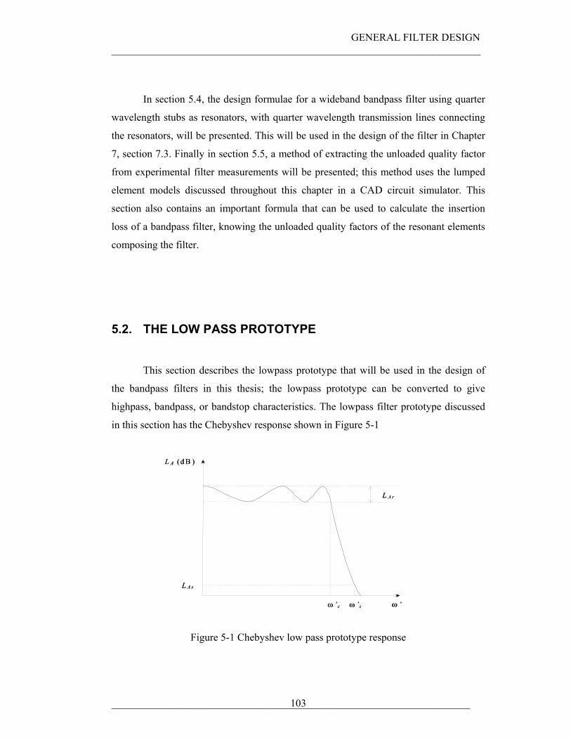
GENERAL FILTER DESIGN ______________________________________________________________________
____________________________________________________________________ 103
In section 5.4, the design formulae for a wideband bandpass filter using quarter
wavelength stubs as resonators, with quarter wavelength transmission lines connecting
the resonators, will be presented. This will be used in the design of the filter in Chapter
7, section 7.3. Finally in section 5.5, a method of extracting the unloaded quality factor
from experimental filter measurements will be presented; this method uses the lumped
element models discussed throughout this chapter in a CAD circuit simulator. This
section also contains an important formula that can be used to calculate the insertion
loss of a bandpass filter, knowing the unloaded quality factors of the resonant elements
composing the filter.
5.2. THE LOW PASS PROTOTYPE
This section describes the lowpass prototype that will be used in the design of
the bandpass filters in this thesis; the lowpass prototype can be converted to give
highpass, bandpass, or bandstop characteristics. The lowpass filter prototype discussed
in this section has the Chebyshev response shown in Figure 5-1
L A r
L A (d B )
ω ’s ω ’c
L A s
ω ’
Figure 5-1 Chebyshev low pass prototype response
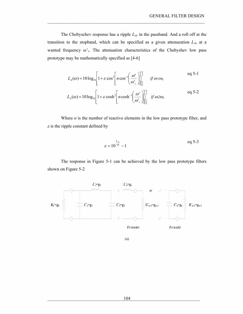
GENERAL FILTER DESIGN ______________________________________________________________________
____________________________________________________________________ 104
The Chebyschev response has a ripple LAr in the passband. And a roll off at the
transition to the stopband, which can be specified as a given attenueation LAs at a
wanted frequency ω’s. The attenuation characteristics of the Chebyshev low pass
prototype may be mathematically specified as [4-6]
⎥⎥⎦
⎤
⎢⎢⎣
⎡
⎥⎥⎦
⎤
⎢⎢⎣
⎡⎟⎟⎠
⎞⎜⎜⎝
⎛+= −
cA nL
''coscos1log10)( 12
10 ωωεω if ω<ωc
eq 5-1
⎥⎥⎦
⎤
⎢⎢⎣
⎡
⎥⎥⎦
⎤
⎢⎢⎣
⎡⎟⎟⎠
⎞⎜⎜⎝
⎛+= −
cA nL
''coshcosh1log10)( 12
10 ωωεω if ω≥ωc
eq 5-2
Where n is the number of reactive elements in the low pass prototype filter, and
ε is the ripple constant defined by
110 10 −=ArL
ε eq 5-3
The response in Figure 5-1 can be achieved by the low pass prototype filters
shown on Figure 5-2
R0’=g0 C’1=g1
L’2=g2
C’3=g3
L’n=gn
G’n+1=gn+1 C’n=gn R’n+1=gn+1
or
If n is even If n is odd
(a)
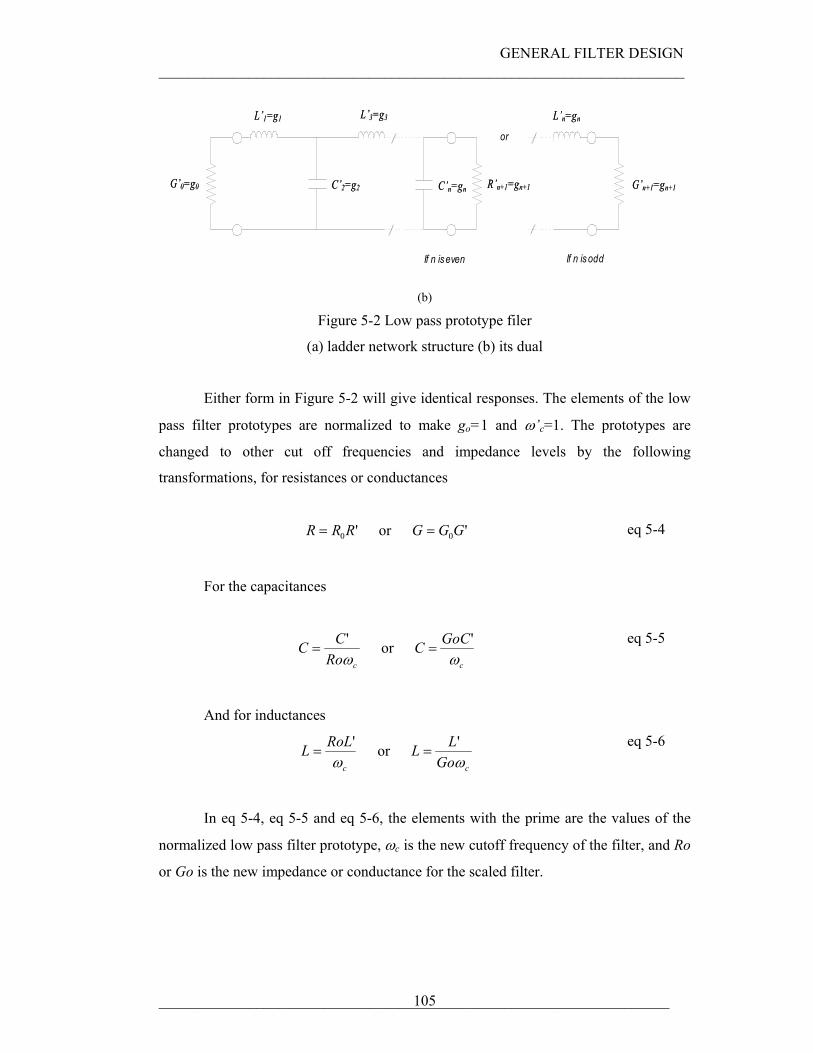
GENERAL FILTER DESIGN ______________________________________________________________________
____________________________________________________________________ 105
G’0=g0 C’2=g2 C’n=gn R’n+1=gn+1 G’n+1=gn+1
L’1=g1 L’3=g3 L’n=gn
or
If n is even If n is odd
(b)
Figure 5-2 Low pass prototype filer
(a) ladder network structure (b) its dual
Either form in Figure 5-2 will give identical responses. The elements of the low
pass filter prototypes are normalized to make go=1 and ω’c=1. The prototypes are
changed to other cut off frequencies and impedance levels by the following
transformations, for resistances or conductances
'0RRR = or '0GGG = eq 5-4
For the capacitances
cRoCCω'
= or c
GoCCω
'= eq 5-5
And for inductances
c
RoLLω
'= or
cGoLLω'
= eq 5-6
In eq 5-4, eq 5-5 and eq 5-6, the elements with the prime are the values of the
normalized low pass filter prototype, ωc is the new cutoff frequency of the filter, and Ro
or Go is the new impedance or conductance for the scaled filter.
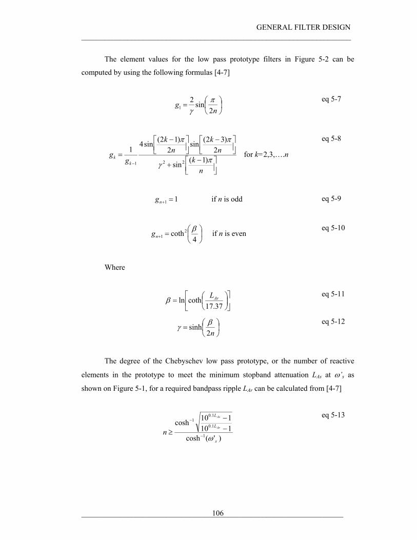
GENERAL FILTER DESIGN ______________________________________________________________________
____________________________________________________________________ 106
The element values for the low pass prototype filters in Figure 5-2 can be
computed by using the following formulas [4-7]
⎟⎠⎞
⎜⎝⎛=
ng
2sin2
1π
γ
eq 5-7
⎥⎦⎤
⎢⎣⎡ −
+
⎥⎦⎤
⎢⎣⎡ −
⎥⎦⎤
⎢⎣⎡ −
=−
nk
nk
nk
gg
kk πγ
ππ
)1(sin
2)32(sin
2)12(sin4
1221
for k=2,3,….n
eq 5-8
11 =+ng if n is odd
eq 5-9
⎟⎠⎞
⎜⎝⎛=+ 4
coth21
βng if n is even
eq 5-10
Where
⎥⎦
⎤⎢⎣
⎡⎟⎠⎞
⎜⎝⎛=
37.17cothln ArLβ
eq 5-11
⎟⎠⎞
⎜⎝⎛=
n2sinh βγ
eq 5-12
The degree of the Chebyschev low pass prototype, or the number of reactive
elements in the prototype to meet the minimum stopband attenuation LAs at ω’s as
shown on Figure 5-1, for a required bandpass ripple LAr can be calculated from [4-7]
)'(cosh110110cosh
1
1.0
1.01
s
L
L
Ar
As
nω−
−
−−
≥
eq 5-13
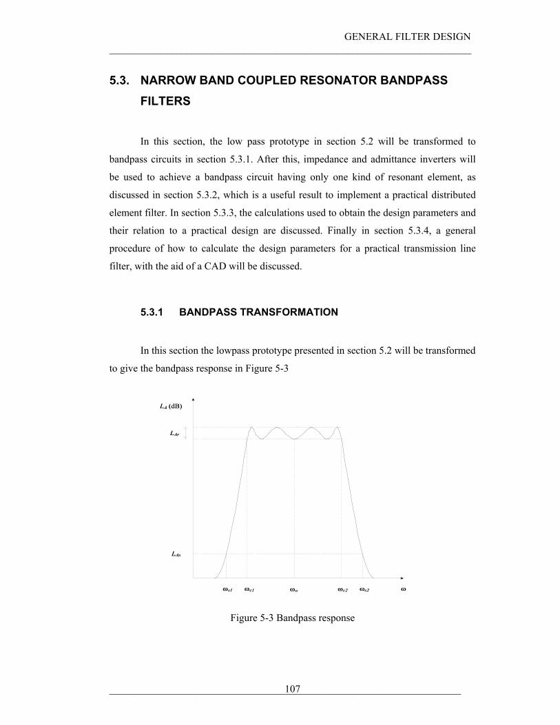
GENERAL FILTER DESIGN ______________________________________________________________________
____________________________________________________________________ 107
5.3. NARROW BAND COUPLED RESONATOR BANDPASS FILTERS
In this section, the low pass prototype in section 5.2 will be transformed to
bandpass circuits in section 5.3.1. After this, impedance and admittance inverters will
be used to achieve a bandpass circuit having only one kind of resonant element, as
discussed in section 5.3.2, which is a useful result to implement a practical distributed
element filter. In section 5.3.3, the calculations used to obtain the design parameters and
their relation to a practical design are discussed. Finally in section 5.3.4, a general
procedure of how to calculate the design parameters for a practical transmission line
filter, with the aid of a CAD will be discussed.
5.3.1 BANDPASS TRANSFORMATION
In this section the lowpass prototype presented in section 5.2 will be transformed
to give the bandpass response in Figure 5-3
LAr
LAs
LA (dB)
ωc1 ωc2 ωo ωs1 ωs2 ω
Figure 5-3 Bandpass response
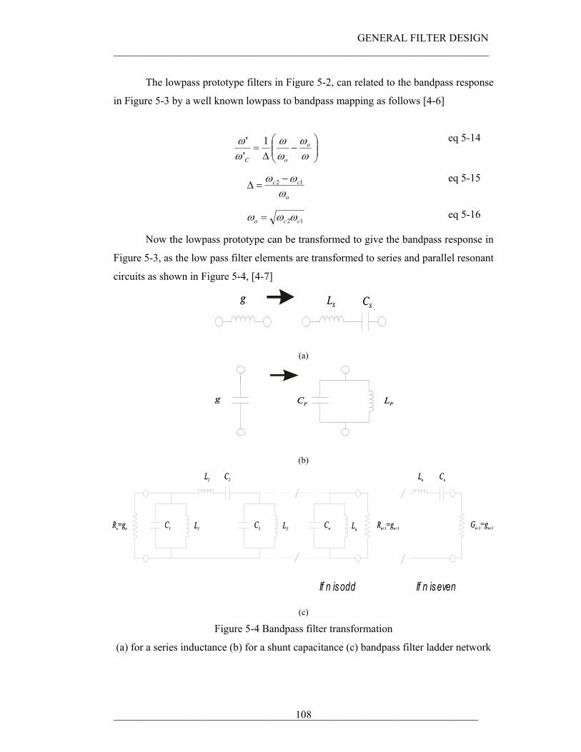
GENERAL FILTER DESIGN ______________________________________________________________________
____________________________________________________________________ 108
The lowpass prototype filters in Figure 5-2, can related to the bandpass response
in Figure 5-3 by a well known lowpass to bandpass mapping as follows [4-6]
⎟⎟⎠
⎞⎜⎜⎝
⎛−
∆=
ωω
ωω
ωω o
oC
1''
eq 5-14
o
cc
ωωω 12 −=∆ eq 5-15
12 cco ωωω = eq 5-16
Now the lowpass prototype can be transformed to give the bandpass response in
Figure 5-3, as the low pass filter elements are transformed to series and parallel resonant
circuits as shown in Figure 5-4, [4-7]
g LS CS
(a)
LPg CP
(b)
Ro=go Rn+1=gn+1 Gn+1=gn+1 L1 C1
C2 L2
L3 C3 Cn Ln
Ln Cn
If n is odd If n is even
(c)
Figure 5-4 Bandpass filter transformation
(a) for a series inductance (b) for a shunt capacitance (c) bandpass filter ladder network
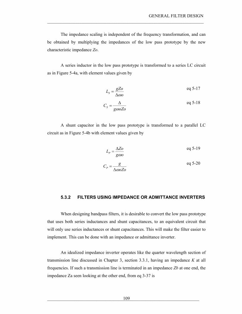
GENERAL FILTER DESIGN ______________________________________________________________________
____________________________________________________________________ 109
The impedance scaling is independent of the frequency transformation, and can
be obtained by multiplying the impedances of the low pass prototype by the new
characteristic impedance Zo.
A series inductor in the low pass prototype is transformed to a series LC circuit
as in Figure 5-4a, with element values given by
ogZoLS ω∆
= eq 5-17
oZogCS ω
∆= eq 5-18
A shunt capacitor in the low pass prototype is transformed to a parallel LC
circuit as in Figure 5-4b with element values given by
ogZoLP ω
∆= eq 5-19
oZogCP ω∆
= eq 5-20
5.3.2 FILTERS USING IMPEDANCE OR ADMITTANCE INVERTERS
When designing bandpass filters, it is desirable to convert the low pass prototype
that uses both series inductances and shunt capacitances, to an equivalent circuit that
will only use series inductances or shunt capacitances. This will make the filter easier to
implement. This can be done with an impedance or admittance inverter.
An idealized impedance inverter operates like the quarter wavelength section of
transmission line discussed in Chapter 3, section 3.3.1, having an impedance K at all
frequencies. If such a transmission line is terminated in an impedance Zb at one end, the
impedance Za seen looking at the other end, from eq 3-37 is
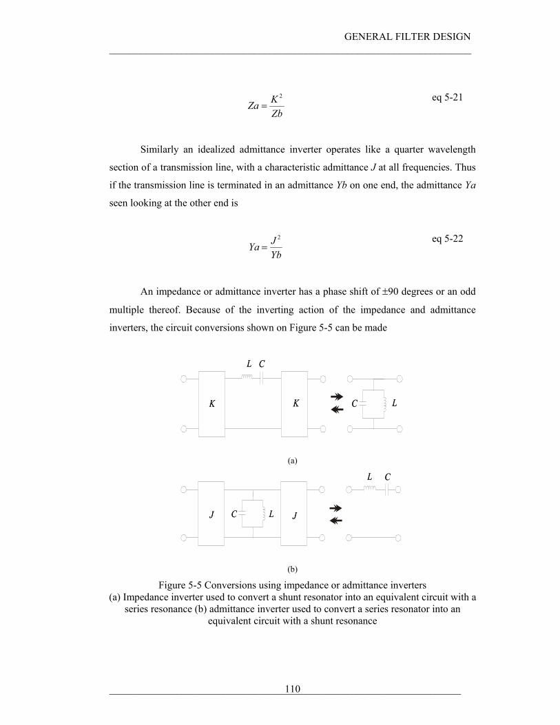
GENERAL FILTER DESIGN ______________________________________________________________________
____________________________________________________________________ 110
ZbKZa
2
= eq 5-21
Similarly an idealized admittance inverter operates like a quarter wavelength
section of a transmission line, with a characteristic admittance J at all frequencies. Thus
if the transmission line is terminated in an admittance Yb on one end, the admittance Ya
seen looking at the other end is
YbJYa
2
= eq 5-22
An impedance or admittance inverter has a phase shift of ±90 degrees or an odd
multiple thereof. Because of the inverting action of the impedance and admittance
inverters, the circuit conversions shown on Figure 5-5 can be made
L K
C
K C
L
(a)
C
J JC L
L
(b)
Figure 5-5 Conversions using impedance or admittance inverters (a) Impedance inverter used to convert a shunt resonator into an equivalent circuit with a
series resonance (b) admittance inverter used to convert a series resonator into an equivalent circuit with a shunt resonance
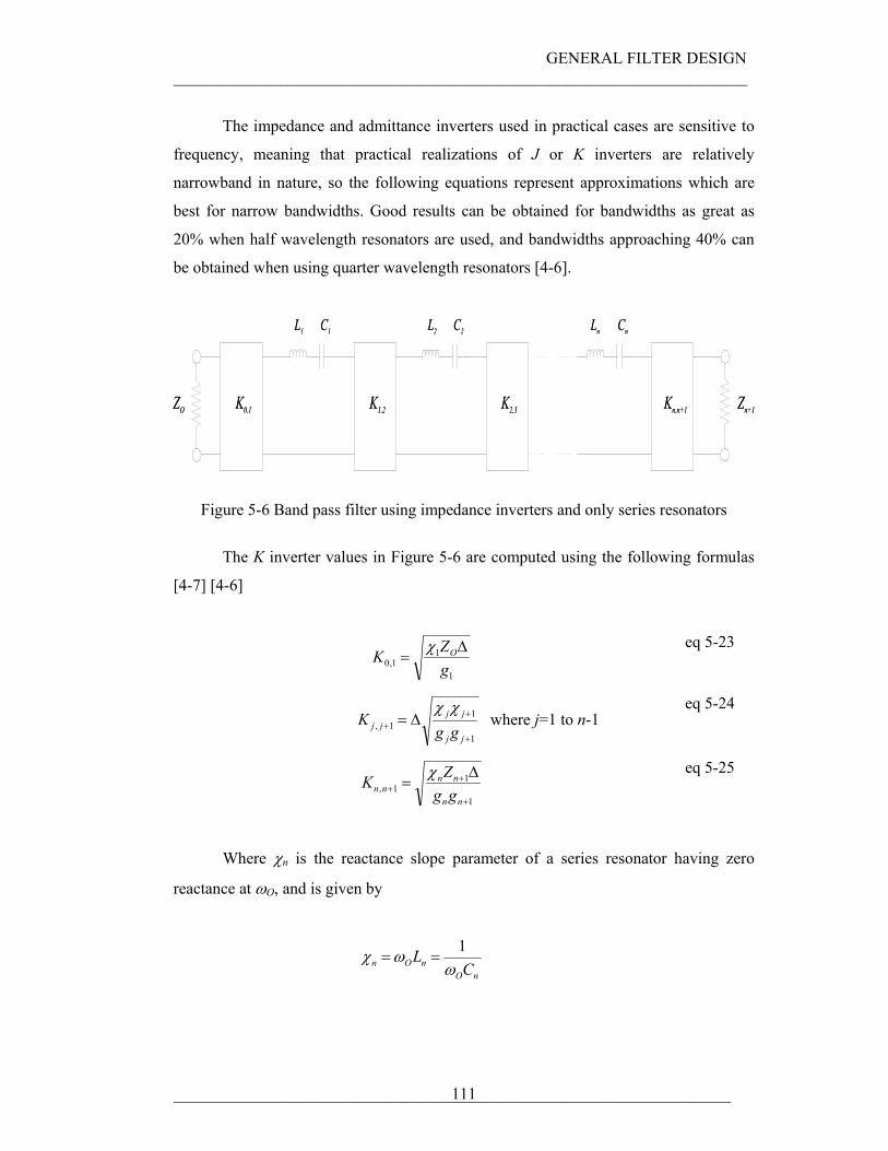
GENERAL FILTER DESIGN ______________________________________________________________________
____________________________________________________________________ 111
The impedance and admittance inverters used in practical cases are sensitive to
frequency, meaning that practical realizations of J or K inverters are relatively
narrowband in nature, so the following equations represent approximations which are
best for narrow bandwidths. Good results can be obtained for bandwidths as great as
20% when half wavelength resonators are used, and bandwidths approaching 40% can
be obtained when using quarter wavelength resonators [4-6].
C1 L1 L2 C2 Ln Cn
K0,1 K1,2 K2,3 Kn,n+1 ZO Zn+1
Figure 5-6 Band pass filter using impedance inverters and only series resonators
The K inverter values in Figure 5-6 are computed using the following formulas
[4-7] [4-6]
1
11,0 g
ZK O∆=χ
eq 5-23
1
11,
+
++ ∆=
jj
jjjj gg
Kχχ
where j=1 to n-1 eq 5-24
1
11,
+
++
∆=
nn
nnnn gg
ZK χ eq 5-25
Where χn is the reactance slope parameter of a series resonator having zero
reactance at ωO, and is given by
nOnOn C
Lω
ωχ 1==
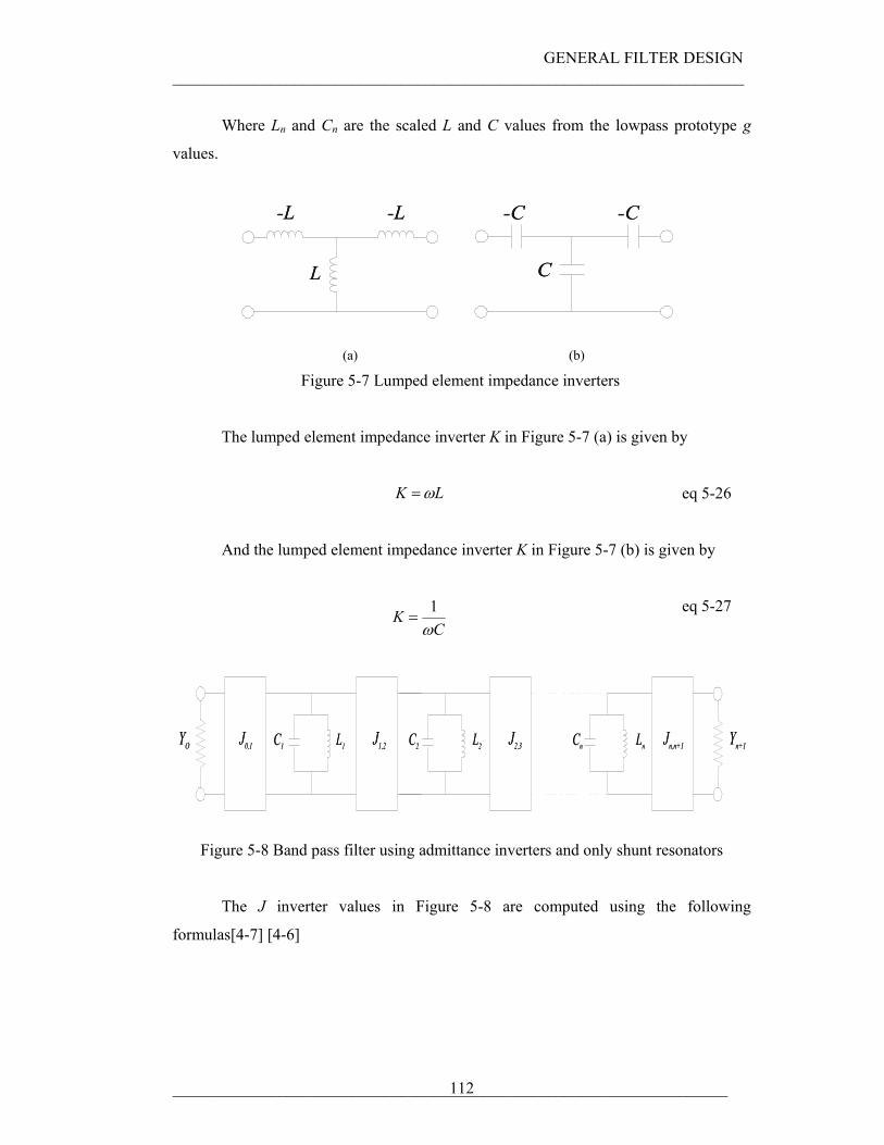
GENERAL FILTER DESIGN ______________________________________________________________________
____________________________________________________________________ 112
Where Ln and Cn are the scaled L and C values from the lowpass prototype g
values.
L
-L -L
-C -C
C
(a) (b)
Figure 5-7 Lumped element impedance inverters
The lumped element impedance inverter K in Figure 5-7 (a) is given by
LK ω= eq 5-26
And the lumped element impedance inverter K in Figure 5-7 (b) is given by
CK
ω1
= eq 5-27
L1 C1 L2C2 Ln Cn Jn,n+1 J0,1 J1,2 J2,3 Yn+1 YO
Figure 5-8 Band pass filter using admittance inverters and only shunt resonators
The J inverter values in Figure 5-8 are computed using the following
formulas[4-7] [4-6]
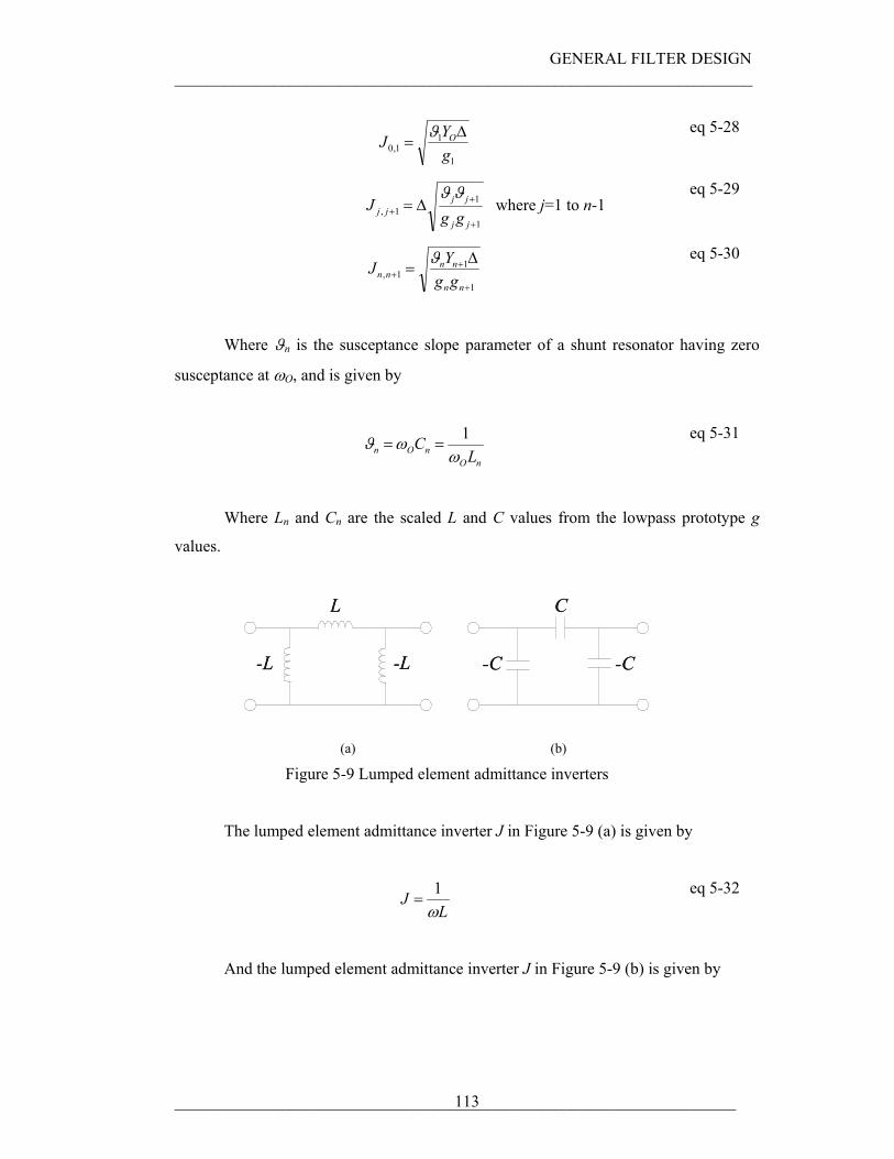
GENERAL FILTER DESIGN ______________________________________________________________________
____________________________________________________________________ 113
1
11,0 g
YJ O∆=ϑ
eq 5-28
1
11,
+
++ ∆=
jj
jjjj gg
Jϑϑ
where j=1 to n-1 eq 5-29
1
11,
+
++
∆=
nn
nnnn gg
YJ ϑ eq 5-30
Where ϑn is the susceptance slope parameter of a shunt resonator having zero
susceptance at ωO, and is given by
nOnOn L
Cω
ωϑ 1== eq 5-31
Where Ln and Cn are the scaled L and C values from the lowpass prototype g
values.
L
-L -L
-C -C
C
(a) (b)
Figure 5-9 Lumped element admittance inverters
The lumped element admittance inverter J in Figure 5-9 (a) is given by
LJ
ω1
= eq 5-32
And the lumped element admittance inverter J in Figure 5-9 (b) is given by
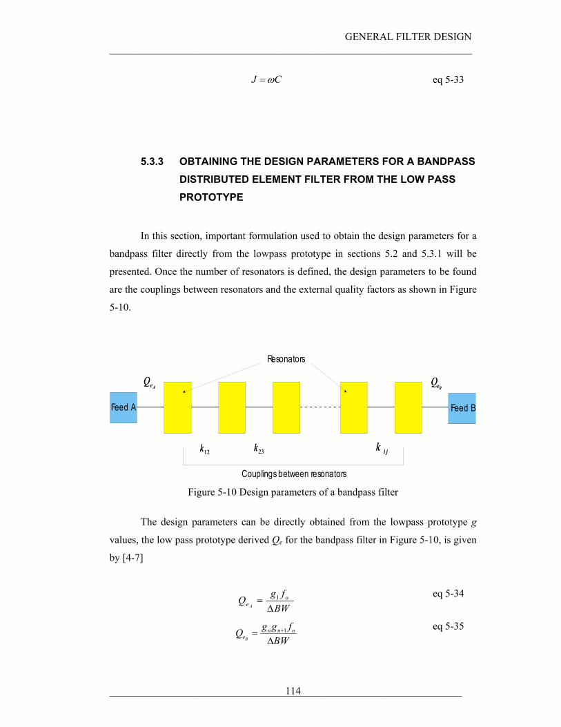
GENERAL FILTER DESIGN ______________________________________________________________________
____________________________________________________________________ 114
CJ ω= eq 5-33
5.3.3 OBTAINING THE DESIGN PARAMETERS FOR A BANDPASS DISTRIBUTED ELEMENT FILTER FROM THE LOW PASS PROTOTYPE
In this section, important formulation used to obtain the design parameters for a
bandpass filter directly from the lowpass prototype in sections 5.2 and 5.3.1 will be
presented. Once the number of resonators is defined, the design parameters to be found
are the couplings between resonators and the external quality factors as shown in Figure
5-10.
AeQBeQ
12k 23k i jk
AeQBeQ
12k 23k i jk
Couplings between resonators
Feed A Feed B
Resonators
Figure 5-10 Design parameters of a bandpass filter
The design parameters can be directly obtained from the lowpass prototype g
values, the low pass prototype derived Qe for the bandpass filter in Figure 5-10, is given
by [4-7]
BWfgQ o
e A ∆= 1 eq 5-34
BWfggQ onn
eB ∆= +1
eq 5-35
GENERAL FILTER DESIGN ______________________________________________________________________
____________________________________________________________________ 115
Where fo in eq 5-34 and eq 5-35 is the desired centre frequency for the bandpass
filter response, the g’s are the low pass element values, and ∆BW is the desired
bandpass bandwidth for the filter as in Figure 5-3 given by
12 CCBW ωω −=∆ eq 5-36
Next, the coupling coefficients derived from the low pass prototype are given by
[4-7]
jioij ggf
BWk ∆= eq 5-37
Where fo in eq 5-37 is the desired centre frequency for the bandpass filter
response, ∆BW is the desired bandpass bandwidth for the filter as in Figure 5-3, given
by eq 5-36, and the g’s are the low pass element values.
5.3.4 DETERMINATION OF COUPLINGS WITH THE AID OF A CAD SIMULATOR
In this section, important formulation will be presented to calculate the
couplings within a practical filter. The couplings will be computed with the aid of an
electromagnetic CAD simulator, to match the ones obtained directly from the low pass
element g values, described in section 5.3.3. The details of how the parameters were
calculated for each filter of this thesis will be discussed in Chapter 7. Here only the
main procedure will be addressed, with the example of coupled microstrip resonators.
The parameters involved in filter design are the couplings between the
resonators, and the external quality factors. By determining these parameters, the
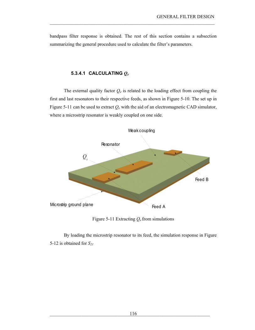
GENERAL FILTER DESIGN ______________________________________________________________________
____________________________________________________________________ 116
bandpass filter response is obtained. The rest of this section contains a subsection
summarizing the general procedure used to calculate the filter’s parameters.
5.3.4.1 CALCULATING Qe
The external quality factor Qe is related to the loading effect from coupling the
first and last resonators to their respective feeds, as shown in Figure 5-10. The set up in
Figure 5-11 can be used to extract Qe with the aid of an electromagnetic CAD simulator,
where a microstrip resonator is weakly coupled on one side.
Microstrip ground plane
Resonator
Weak coupling
Feed A
Feed B
Figure 5-11 Extracting Qe from simulations
By loading the microstrip resonator to its feed, the simulation response in Figure
5-12 is obtained for S21
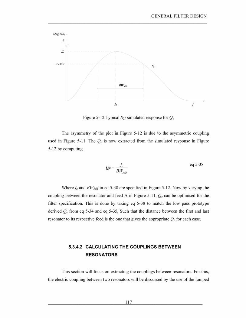
GENERAL FILTER DESIGN ______________________________________________________________________
____________________________________________________________________ 117
BW3dB
S21
f fo
IL-3dB
IL
Mag (dB)
0
Figure 5-12 Typical S21 simulated response for Qe
The asymmetry of the plot in Figure 5-12 is due to the asymmetric coupling
used in Figure 5-11. The Qe is now extracted from the simulated response in Figure
5-12 by computing
dB
o
BWfQe
3
= eq 5-38
Where fo and BW3dB in eq 5-38 are specified in Figure 5-12. Now by varying the
coupling between the resonator and feed A in Figure 5-11, Qe can be optimised for the
filter specification. This is done by taking eq 5-38 to match the low pass prototype
derived Qe from eq 5-34 and eq 5-35, Such that the distance between the first and last
resonator to its respective feed is the one that gives the appropriate Qe for each case.
5.3.4.2 CALCULATING THE COUPLINGS BETWEEN RESONATORS
This section will focus on extracting the couplings between resonators. For this,
the electric coupling between two resonators will be discussed by the use of the lumped
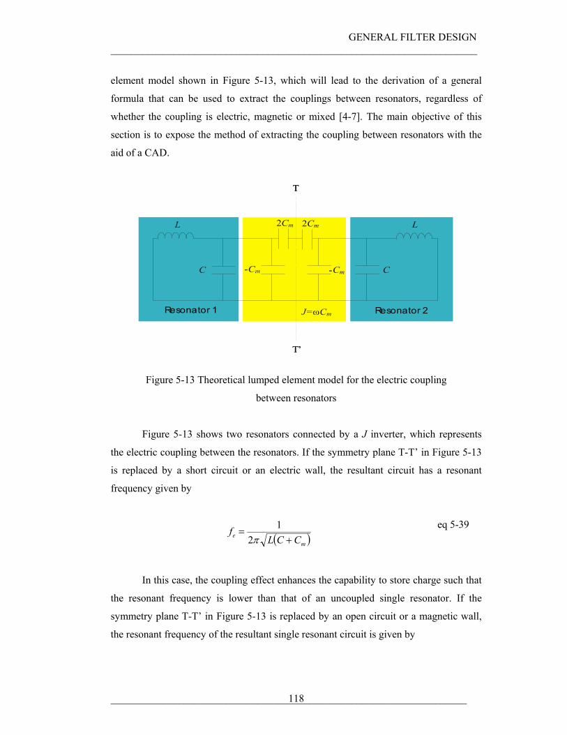
GENERAL FILTER DESIGN ______________________________________________________________________
____________________________________________________________________ 118
element model shown in Figure 5-13, which will lead to the derivation of a general
formula that can be used to extract the couplings between resonators, regardless of
whether the coupling is electric, magnetic or mixed [4-7]. The main objective of this
section is to expose the method of extracting the coupling between resonators with the
aid of a CAD.
T
T’
2Cm 2Cm
-Cm -Cm C C
L L
J=ωCm Resonator 1 Resonator 2
Figure 5-13 Theoretical lumped element model for the electric coupling
between resonators
Figure 5-13 shows two resonators connected by a J inverter, which represents
the electric coupling between the resonators. If the symmetry plane T-T’ in Figure 5-13
is replaced by a short circuit or an electric wall, the resultant circuit has a resonant
frequency given by
( )me CCL
f+
=π2
1 eq 5-39
In this case, the coupling effect enhances the capability to store charge such that
the resonant frequency is lower than that of an uncoupled single resonator. If the
symmetry plane T-T’ in Figure 5-13 is replaced by an open circuit or a magnetic wall,
the resonant frequency of the resultant single resonant circuit is given by
GENERAL FILTER DESIGN ______________________________________________________________________
____________________________________________________________________ 119
( )mm CCL
f−
=π2
1 eq 5-40
In this case, the coupling effect reduces the capability to store charge, such that
the resonant frequency with respect of an uncoupled single resonator is increased. Now
by using eq 5-39 and eq 5-40, the electric coupling coefficient between the resonators of
Figure 5-13 can be found by
CC
ffffk m
em
emE =
+−
= 22
22
eq 5-41
As mentioned at the beginning of this section, a magnetic and a mixed coupling
between resonators can also be defined; these models all converge in a general
expression for the coupling between resonators eq 5-42, which will be treated in the rest
of this section with the example of coupled microstrip resonators.
The set up in Figure 5-14 can be used to extract the couplings between the two
microstrip resonators, with the aid of an electromagnetic CAD simulator. The resonators
should be weakly coupled to their feeds in order to extract the coupling between the
resonators.
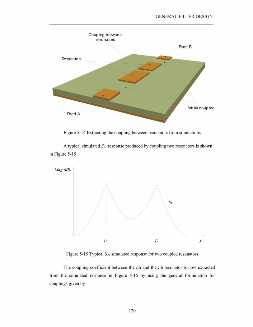
GENERAL FILTER DESIGN ______________________________________________________________________
____________________________________________________________________ 120
Resonators
Feed A
Feed B
Weak coupling
Coupling between resonators
Figure 5-14 Extracting the coupling between resonators from simulations
A typical simulated S21 response produced by coupling two resonators is shown
in Figure 5-15
Mag (dB)
f f2 f1
S21
Figure 5-15 Typical S21 simulated response for two coupled resonators
The coupling coefficient between the ith and the jth resonator is now extracted
from the simulated response in Figure 5-15 by using the general formulation for
couplings given by
GENERAL FILTER DESIGN ______________________________________________________________________
____________________________________________________________________ 121
21
22
21
22
ffffkij +
−=
eq 5-42
Where f1 and f2 are the frequencies of the two coupled peaks generated by the
electromagnetic interaction between the resonators as shown in Figure 5-15. Now by
varying the coupling between resonators, the value of the couplings is optimised to the
filter specification by making the coupling of eq 5-42 match the coupling coefficients
derived from the low pass prototype, which are given by eq 5-37. With this data, the
appropriate distances between resonators can be calculated.
5.4. WIDEBAND FILTER USING QUARTER WAVELENGTH STUBS
In this section, the design formulae for a wideband bandpass filter using quarter
wavelength short circuited stubs as resonators, and quarter wavelength transmission
lines connecting the resonators as admittance inverters will be introduced.
The filter in this section has an identical bandpass ladder network to the one
shown on Figure 5-8. Here the shunt resonators are implemented by quarter wavelength
long transmission lines. The resonators are connected by quarter wavelength long
sections of transmission line, as admittance inverters.
This filter structure is not good for narrow band filters, as the stubs will have
unreasonably low impedance levels, as the bandwidth becomes narrower. The filter
structure defined in this section is shown on Figure 5-16.
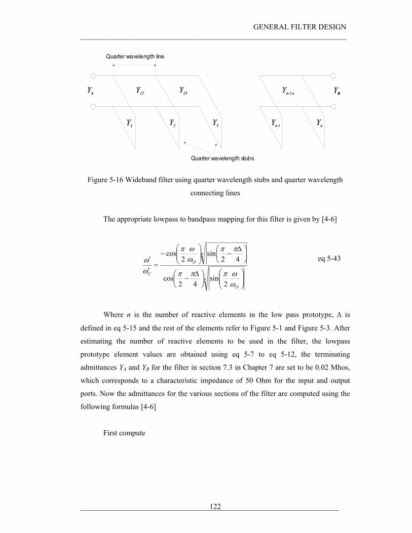
GENERAL FILTER DESIGN ______________________________________________________________________
____________________________________________________________________ 122
YA YB
Y1 Y2 Y3 Yn
Y12 Y23
Yn-1
Yn-1,n
Quarter wavelength line
Quarter wavelength stubs
Figure 5-16 Wideband filter using quarter wavelength stubs and quarter wavelength
connecting lines
The appropriate lowpass to bandpass mapping for this filter is given by [4-6]
n
O
n
O
C
⎟⎟⎠
⎞⎜⎜⎝
⎛⎟⎠⎞
⎜⎝⎛ ∆
−
⎟⎠⎞
⎜⎝⎛ ∆
−⎟⎟⎠
⎞⎜⎜⎝
⎛−
=′′
ωωπππ
ππωωπ
ωω
2sin
42cos
42sin
2cos
eq 5-43
Where n is the number of reactive elements in the low pass prototype, ∆ is
defined in eq 5-15 and the rest of the elements refer to Figure 5-1 and Figure 5-3. After
estimating the number of reactive elements to be used in the filter, the lowpass
prototype element values are obtained using eq 5-7 to eq 5-12, the terminating
admittances YA and YB for the filter in section 7.3 in Chapter 7 are set to be 0.02 Mhos,
which corresponds to a characteristic impedance of 50 Ohm for the input and output
ports. Now the admittances for the various sections of the filter are computed using the
following formulas [4-6]
First compute
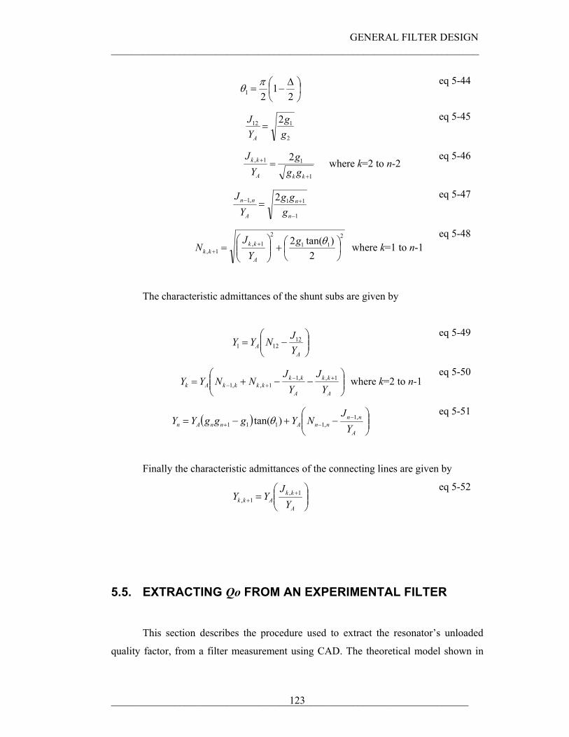
GENERAL FILTER DESIGN ______________________________________________________________________
____________________________________________________________________ 123
⎟⎠⎞
⎜⎝⎛ ∆−=
21
21πθ
eq 5-44
2
112 2gg
YJ
A
= eq 5-45
1
11, 2
+
+ =kkA
kk
ggg
YJ
where k=2 to n-2 eq 5-46
1
11,1 2
−
+− =n
n
A
nn
ggg
YJ
eq 5-47
2
11
21,
1, 2)tan(2⎟⎠⎞
⎜⎝⎛+⎟⎟
⎠
⎞⎜⎜⎝
⎛= +
+θg
YJ
NA
kkkk where k=1 to n-1
eq 5-48
The characteristic admittances of the shunt subs are given by
⎟⎟⎠
⎞⎜⎜⎝
⎛−=
AA Y
JNYY 12121
eq 5-49
⎟⎟⎠
⎞⎜⎜⎝
⎛−−+= +−
+−A
kk
A
kkkkkkAk Y
JY
JNNYY 1,,1
1,,1 where k=2 to n-1 eq 5-50
( ) ⎟⎟⎠
⎞⎜⎜⎝
⎛−+−= −
−+A
nnnnAnnAn Y
JNYgggYY ,1
,1111 )tan(θ eq 5-51
Finally the characteristic admittances of the connecting lines are given by
⎟⎟⎠
⎞⎜⎜⎝
⎛= +
+A
kkAkk Y
JYY 1,
1, eq 5-52
5.5. EXTRACTING Qo FROM AN EXPERIMENTAL FILTER
This section describes the procedure used to extract the resonator’s unloaded
quality factor, from a filter measurement using CAD. The theoretical model shown in
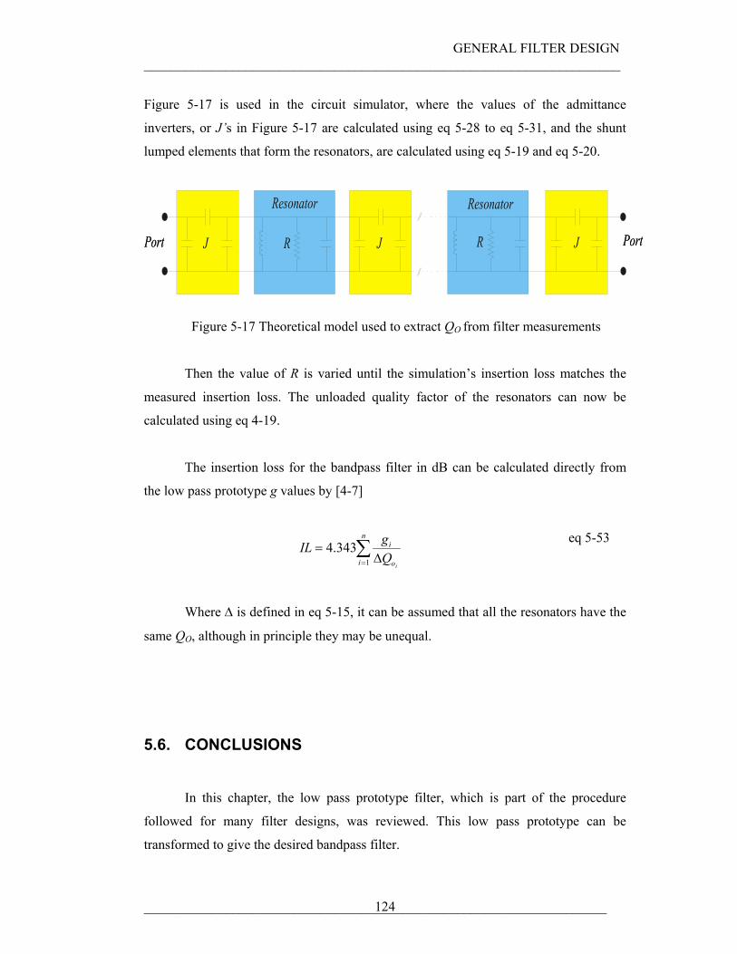
GENERAL FILTER DESIGN ______________________________________________________________________
____________________________________________________________________ 124
Figure 5-17 is used in the circuit simulator, where the values of the admittance
inverters, or J’s in Figure 5-17 are calculated using eq 5-28 to eq 5-31, and the shunt
lumped elements that form the resonators, are calculated using eq 5-19 and eq 5-20.
J J J
Resonator Resonator
Port Port R R
Figure 5-17 Theoretical model used to extract QO from filter measurements
Then the value of R is varied until the simulation’s insertion loss matches the
measured insertion loss. The unloaded quality factor of the resonators can now be
calculated using eq 4-19.
The insertion loss for the bandpass filter in dB can be calculated directly from
the low pass prototype g values by [4-7]
∑= ∆
=n
i o
i
iQgIL
1
343.4 eq 5-53
Where ∆ is defined in eq 5-15, it can be assumed that all the resonators have the
same QO, although in principle they may be unequal.
5.6. CONCLUSIONS
In this chapter, the low pass prototype filter, which is part of the procedure
followed for many filter designs, was reviewed. This low pass prototype can be
transformed to give the desired bandpass filter.
GENERAL FILTER DESIGN ______________________________________________________________________
____________________________________________________________________ 125
After this, the main focus was a discussion of the theory and the main procedure
used to design the filters, which will be described individually in Chapter 7. For this,
theoretical models were presented, as well as the general procedure to set the design
parameters in a simulator.
References [4-7] Jia-Sheng Hong and M.J. Lancaster, [4-6] G. Matthaei
I.Llamas-Garro, PhD thesis (2003), The University of Birmingham, UK
6. CHAPTER SIX
MICROMACHINED TRANSMISSION LINES AND RESONATORS
6.1. INTRODUCTION
In section 6.2 experiments were carried out in order to define a good
transmission line to make the filters described in Chapter 7 will be presented. This
section starts with a shielded microstrip line, followed by a parallel plate waveguide,
and a deep coplanar waveguide and finally the square coaxial transmission line.
In section 6.3 an analytical loss comparison of four transmission lines will be
presented, in which the attenuation constant and the unloaded quality factor for a half
wavelength resonator made out of its respective structure will be calculated and plotted
versus the area of the cross section of the transmission line.
MICROMACHINED TRANSMISSION LINES AND RESONATORS ______________________________________________________________________
____________________________________________________________________ 127
6.2. THE SEARCH FOR A HIGH Q TRANSMISSION LINE
In this section the steps that lead to the choice of the square coaxial transmission
line structure from which the filters in Chapter 7 are made of, will be addressed. A
number of transmission lines have been investigated experimentally. The objective was
to look at different low loss transmission lines at low frequencies with test materials,
with the aim to produce low loss transmission lines at higher frequencies later, made out
of silicon or SU8 for example.
6.2.1 THE SHELDED MICROSTRIP RESONATOR
The first experiment that was carried out, was a foam suspended microstrip half
wavelength transmission line resonator shown in Figure 6-1
Duroid
SMA connector
Shielding
Ground plane
Foam
(a)
MICROMACHINED TRANSMISSION LINES AND RESONATORS ______________________________________________________________________
____________________________________________________________________ 128
(1)
(2)
Resonator0.5
13.7
4.9
Duroid 5880thickness = 0.13 mm er = 2.2
Ground plane
Foam
Feeds
1
Distances in mm
(b)
Figure 6-1 Half wavelength resonator on a foam-duroid substrate
(a) the shielded microstrip resonator (b) dimensions
(1) for the resonator (2) side view of the structure
The fabricated resonator has a low loss propagation media which consists of a
1mm foam layer and a 0.13 mm duroid substrate, and the height of the cavity is 8mm
from the duroid substrate. The resonant frequency for the half wavelength resonator is
9.19 GHz and gave a measured Qo of 345. Some of the problems that occurred with this
experiment were that the duroid is so thin that it started to bend very easily and the foam
height was not strictly uniform. The characteristic impedance of a microstrip line can be
calculated using the following formulae [3-2]
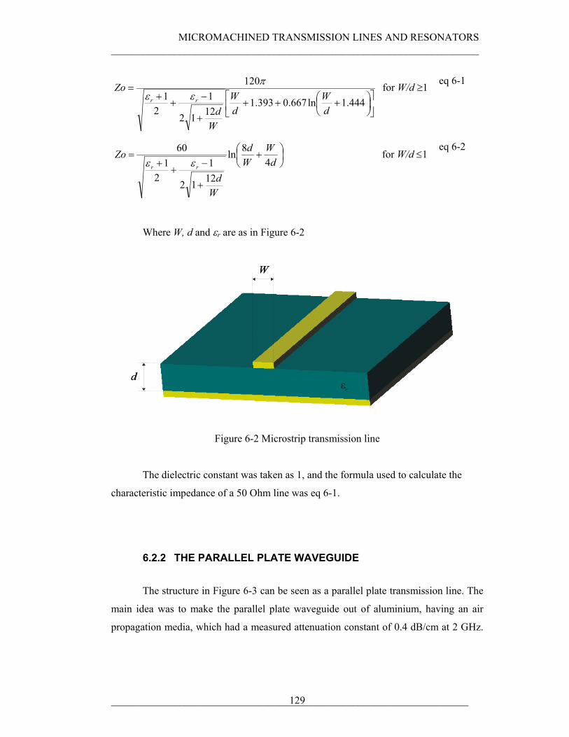
MICROMACHINED TRANSMISSION LINES AND RESONATORS ______________________________________________________________________
____________________________________________________________________ 129
⎥⎦
⎤⎢⎣
⎡⎟⎠⎞
⎜⎝⎛ +++
+
−+
+=
444.1ln667.0393.11212
12
1120
dW
dW
Wd
Zorr εε
π for W/d ≥1 eq 6-1
⎟⎠⎞
⎜⎝⎛ +
+
−+
+=
dW
Wd
Wd
Zorr 4
8ln
1212
12
160
εε for W/d ≤1
eq 6-2
Where W, d and εr are as in Figure 6-2
W
d εr
Figure 6-2 Microstrip transmission line
The dielectric constant was taken as 1, and the formula used to calculate the
characteristic impedance of a 50 Ohm line was eq 6-1.
6.2.2 THE PARALLEL PLATE WAVEGUIDE
The structure in Figure 6-3 can be seen as a parallel plate transmission line. The
main idea was to make the parallel plate waveguide out of aluminium, having an air
propagation media, which had a measured attenuation constant of 0.4 dB/cm at 2 GHz.
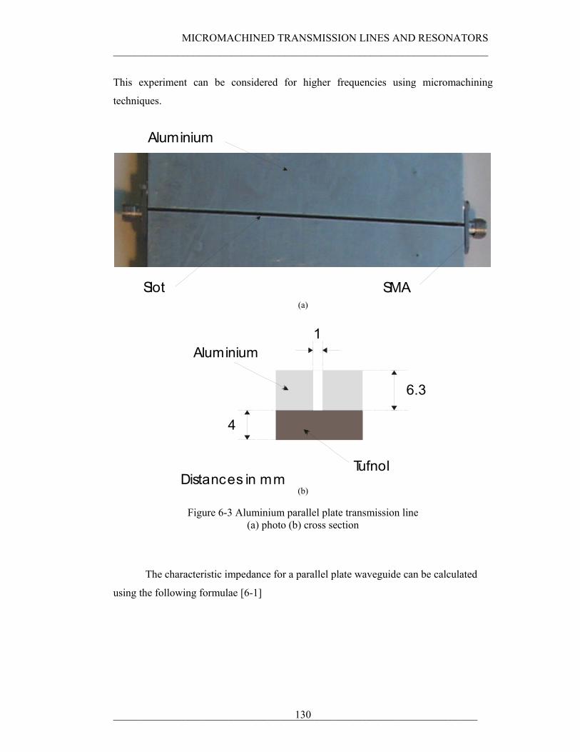
MICROMACHINED TRANSMISSION LINES AND RESONATORS ______________________________________________________________________
____________________________________________________________________ 130
This experiment can be considered for higher frequencies using micromachining
techniques.
Aluminium
SMASlot (a)
Aluminium1
4
6.3
TufnolDistances in mm
(b)
Figure 6-3 Aluminium parallel plate transmission line (a) photo (b) cross section
The characteristic impedance for a parallel plate waveguide can be calculated
using the following formulae [6-1]
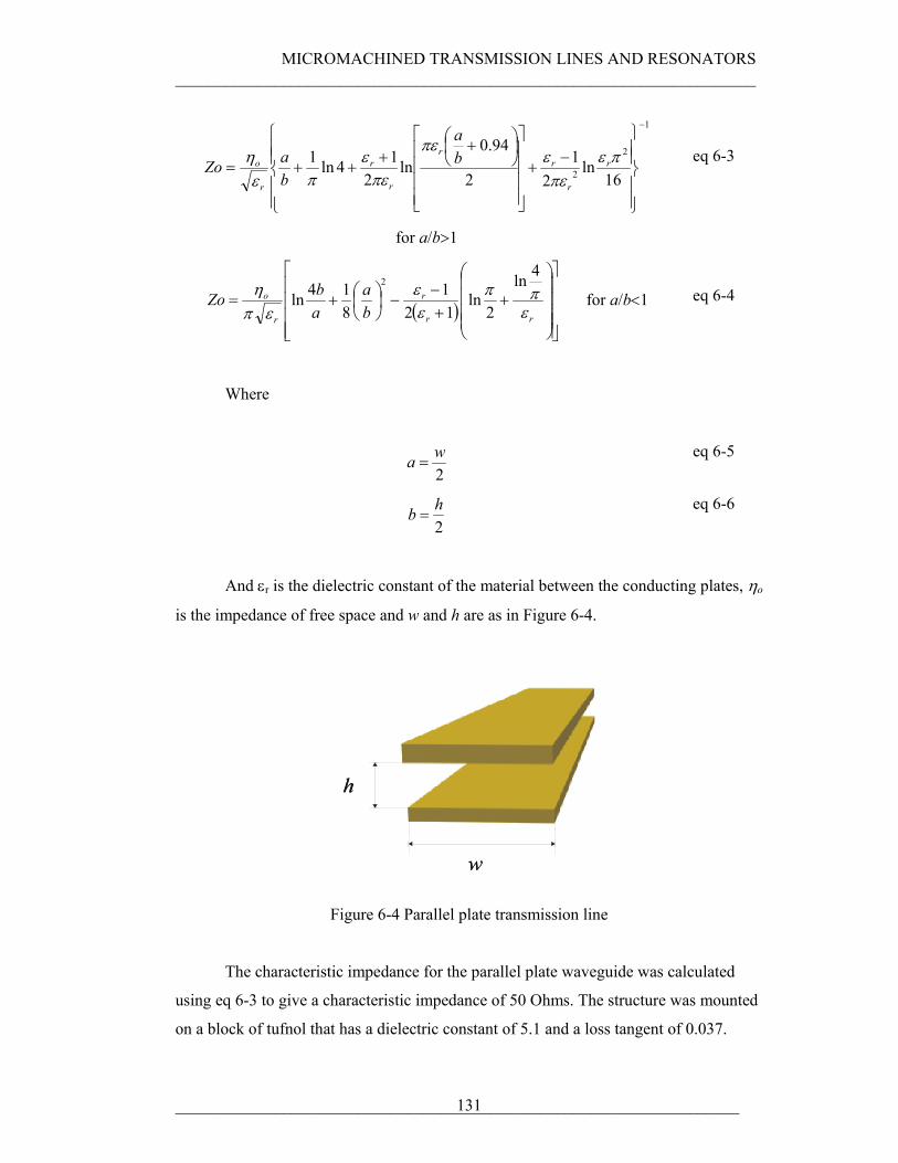
MICROMACHINED TRANSMISSION LINES AND RESONATORS ______________________________________________________________________
____________________________________________________________________ 131
1
2
2 16ln
21
2
94.0ln
214ln1
−
⎪⎪⎭
⎪⎪⎬
⎫
⎪⎪⎩
⎪⎪⎨
⎧−
+
⎥⎥⎥⎥
⎦
⎤
⎢⎢⎢⎢
⎣
⎡⎟⎠⎞
⎜⎝⎛ +
+++=
πεπεε
πε
πεε
πεη r
r
rr
r
r
r
o ba
baZo
for a/b>1
eq 6-3
( )⎥⎥⎥⎥
⎦
⎤
⎢⎢⎢⎢
⎣
⎡
⎟⎟⎟⎟
⎠
⎞
⎜⎜⎜⎜
⎝
⎛
++−
−⎟⎠⎞
⎜⎝⎛+=
rr
r
r
o
ba
abZo
εππ
εε
επη
4ln
2ln
121
814ln
2
for a/b<1
eq 6-4
Where
2wa = eq 6-5
2hb = eq 6-6
And εr is the dielectric constant of the material between the conducting plates, ηo
is the impedance of free space and w and h are as in Figure 6-4.
w
h
Figure 6-4 Parallel plate transmission line
The characteristic impedance for the parallel plate waveguide was calculated
using eq 6-3 to give a characteristic impedance of 50 Ohms. The structure was mounted
on a block of tufnol that has a dielectric constant of 5.1 and a loss tangent of 0.037.
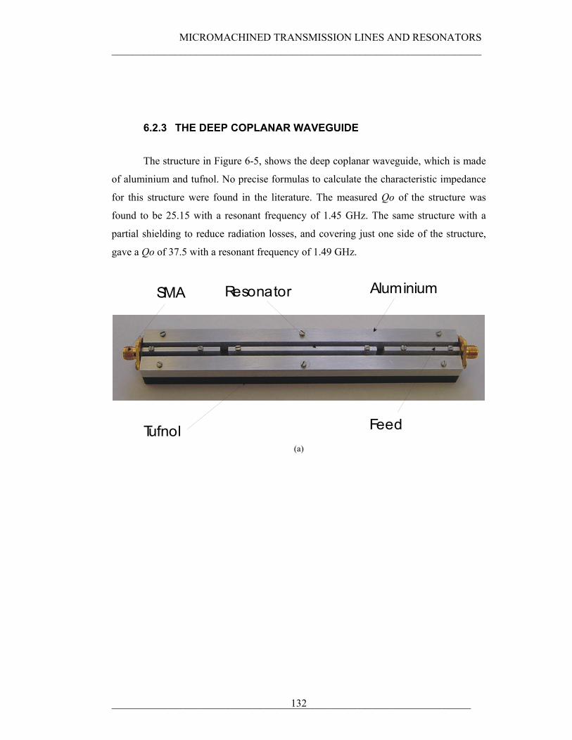
MICROMACHINED TRANSMISSION LINES AND RESONATORS ______________________________________________________________________
____________________________________________________________________ 132
6.2.3 THE DEEP COPLANAR WAVEGUIDE
The structure in Figure 6-5, shows the deep coplanar waveguide, which is made
of aluminium and tufnol. No precise formulas to calculate the characteristic impedance
for this structure were found in the literature. The measured Qo of the structure was
found to be 25.15 with a resonant frequency of 1.45 GHz. The same structure with a
partial shielding to reduce radiation losses, and covering just one side of the structure,
gave a Qo of 37.5 with a resonant frequency of 1.49 GHz.
SMA Resonator
Feed
Aluminium
Tufnol (a)
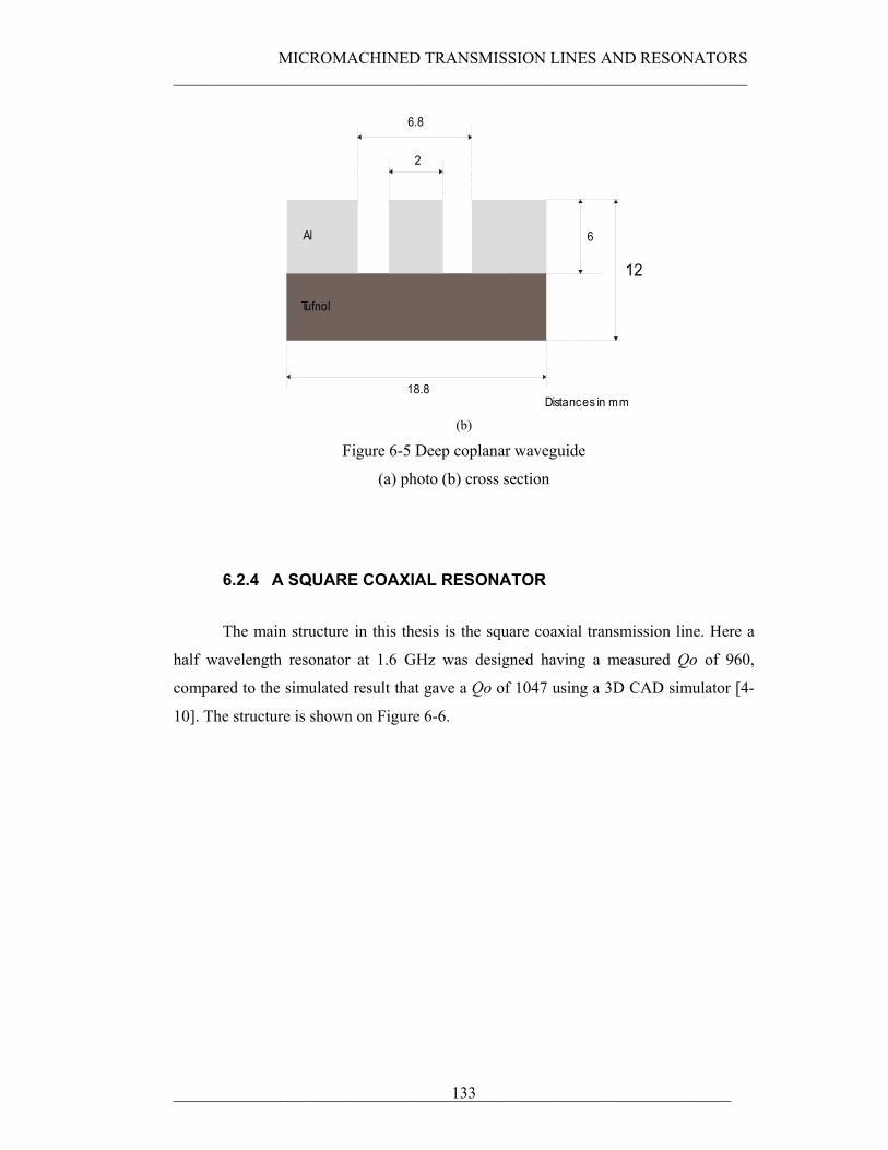
MICROMACHINED TRANSMISSION LINES AND RESONATORS ______________________________________________________________________
____________________________________________________________________ 133
Tufnol
Al
12
6
6.8
2
18.8
Tufnol
Distances in mm (b)
Figure 6-5 Deep coplanar waveguide
(a) photo (b) cross section
6.2.4 A SQUARE COAXIAL RESONATOR
The main structure in this thesis is the square coaxial transmission line. Here a
half wavelength resonator at 1.6 GHz was designed having a measured Qo of 960,
compared to the simulated result that gave a Qo of 1047 using a 3D CAD simulator [4-
10]. The structure is shown on Figure 6-6.
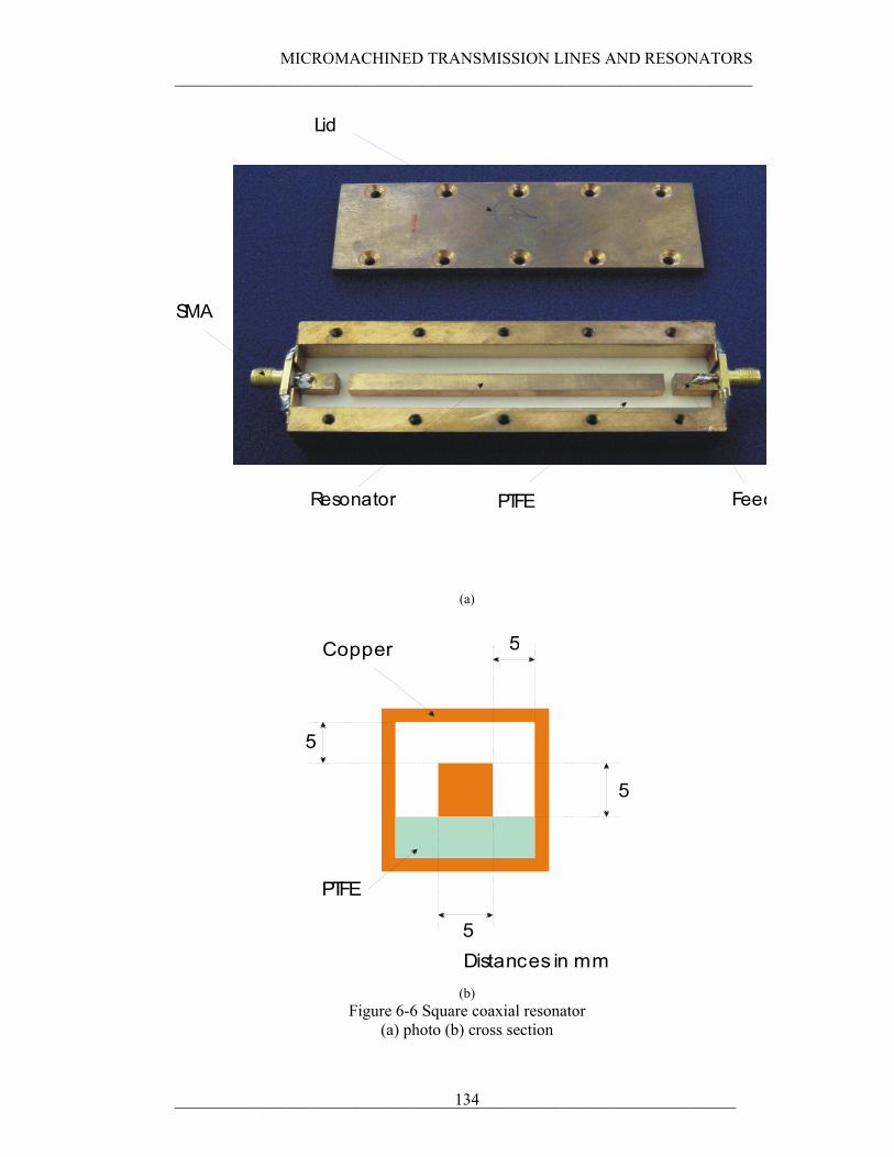
MICROMACHINED TRANSMISSION LINES AND RESONATORS ______________________________________________________________________
____________________________________________________________________ 134
SMA
Lid
Resonator FeedPTFE
(a)
PTFE
5
5
5
5
Copper
Distances in mm
(b) Figure 6-6 Square coaxial resonator
(a) photo (b) cross section
MICROMACHINED TRANSMISSION LINES AND RESONATORS ______________________________________________________________________
____________________________________________________________________ 135
The design equations for a square coaxial transmission line are given in section
6.4. The dielectric used to support the centre conductor is PTFE with a dielectric
constant of 2.1 and a loss tangent of 0.001.
6.3. ANALYTICAL LOSS COMPARISON OF LOW LOSS TRANSMISSION LINES
In this section, a loss comparison between a round coaxial, square coaxial,
microstrip and stripline transmission line resonators will be discussed. This section will
be divided into three sub-subsections. The first one contains the formulae that will be
used to calculate the attenuation constant for the different transmission line structures to
be compared. The second section contains the area of the transmission line’s cross
section that will be considered for comparison between structures in the calculations;
and the third subsection contains the results of the loss comparison between the exposed
structures.
6.3.1 LOW LOSS TRANSMISSION LINES
In this section the focus will be on comparing the conductor loss from the four
structures shown in Figure 6-7. The structures have been compared as if they were
suspended, having no dielectric or radiation loss.
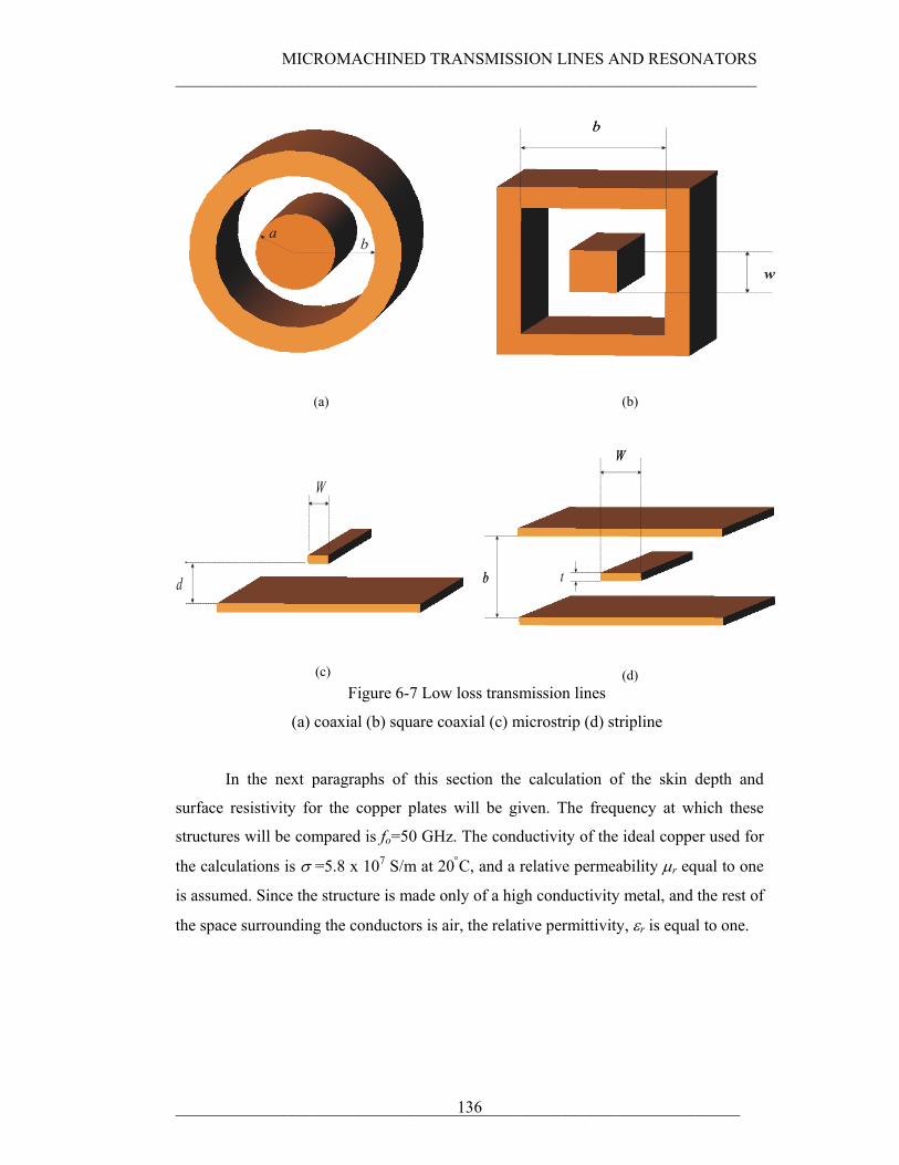
MICROMACHINED TRANSMISSION LINES AND RESONATORS ______________________________________________________________________
____________________________________________________________________ 136
a b
(a)
b
w
(b)
W
d
(c)
t
W
b
(d)
Figure 6-7 Low loss transmission lines
(a) coaxial (b) square coaxial (c) microstrip (d) stripline
In the next paragraphs of this section the calculation of the skin depth and
surface resistivity for the copper plates will be given. The frequency at which these
structures will be compared is fo=50 GHz. The conductivity of the ideal copper used for
the calculations is σ =5.8 x 10⁷ S/m at 20°C, and a relative permeability µr equal to one
is assumed. Since the structure is made only of a high conductivity metal, and the rest of
the space surrounding the conductors is air, the relative permittivity, εr is equal to one.
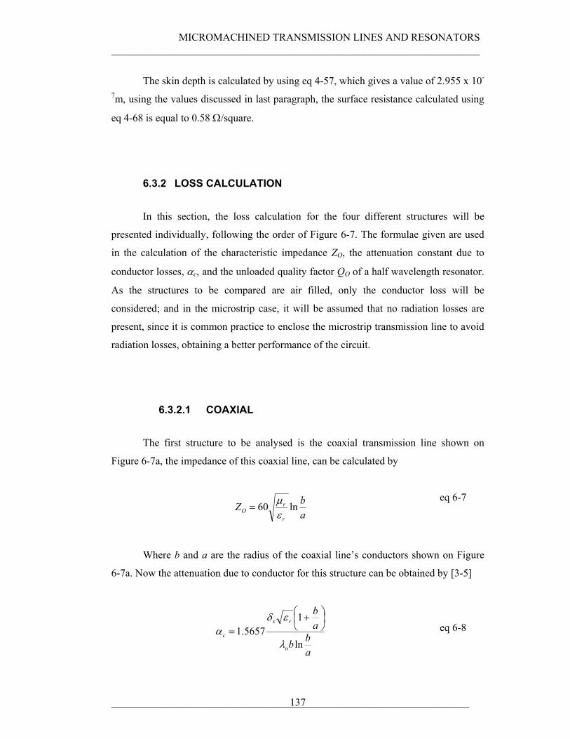
MICROMACHINED TRANSMISSION LINES AND RESONATORS ______________________________________________________________________
____________________________________________________________________ 137
The skin depth is calculated by using eq 4-57, which gives a value of 2.955 x 10-
7m, using the values discussed in last paragraph, the surface resistance calculated using
eq 4-68 is equal to 0.58 Ω/square.
6.3.2 LOSS CALCULATION
In this section, the loss calculation for the four different structures will be
presented individually, following the order of Figure 6-7. The formulae given are used
in the calculation of the characteristic impedance ZO, the attenuation constant due to
conductor losses, αc, and the unloaded quality factor QO of a half wavelength resonator.
As the structures to be compared are air filled, only the conductor loss will be
considered; and in the microstrip case, it will be assumed that no radiation losses are
present, since it is common practice to enclose the microstrip transmission line to avoid
radiation losses, obtaining a better performance of the circuit.
6.3.2.1 COAXIAL
The first structure to be analysed is the coaxial transmission line shown on
Figure 6-7a, the impedance of this coaxial line, can be calculated by
abZ
r
rO ln60
εµ
= eq 6-7
Where b and a are the radius of the coaxial line’s conductors shown on Figure
6-7a. Now the attenuation due to conductor for this structure can be obtained by [3-5]
abb
ab
o
rs
c
ln
15657.1
λ
εδα
⎟⎠⎞
⎜⎝⎛ +
=
eq 6-8
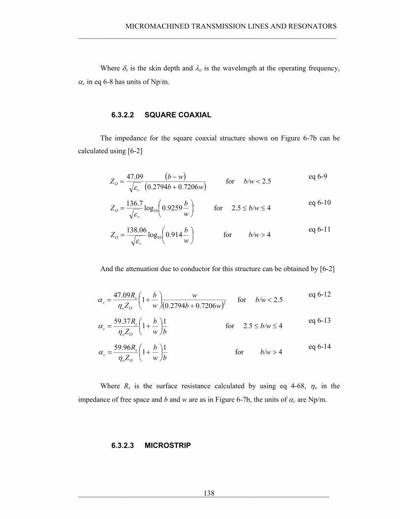
MICROMACHINED TRANSMISSION LINES AND RESONATORS ______________________________________________________________________
____________________________________________________________________ 138
Where δs is the skin depth and λo is the wavelength at the operating frequency,
αc in eq 6-8 has units of Np/m.
6.3.2.2 SQUARE COAXIAL
The impedance for the square coaxial structure shown on Figure 6-7b can be
calculated using [6-2]
( )( )wb
wbZr
O 7206.02794.009.47
+−
=ε
for b/w < 2.5 eq 6-9
⎟⎠⎞
⎜⎝⎛=
wbZ
rO 9259.0log7.136
10ε for 2.5 ≤ b/w ≤ 4
eq 6-10
⎟⎠⎞
⎜⎝⎛=
wbZ
rO 914.0log06.138
10ε for b/w > 4
eq 6-11
And the attenuation due to conductor for this structure can be obtained by [6-2]
( )27206.02794.0109.47
wbw
wb
ZR
Oo
sc +
⎟⎠⎞
⎜⎝⎛ +=
ηα for b/w < 2.5
eq 6-12
bwb
ZR
Oo
sc
1137.59⎟⎠⎞
⎜⎝⎛ +=
ηα for 2.5 ≤ b/w ≤ 4
eq 6-13
bwb
ZR
Oo
sc
1196.59⎟⎠⎞
⎜⎝⎛ +=
ηα for b/w > 4
eq 6-14
Where Rs is the surface resistance calculated by using eq 4-68, ηo in the
impedance of free space and b and w are as in Figure 6-7b, the units of αc are Np/m.
6.3.2.3 MICROSTRIP
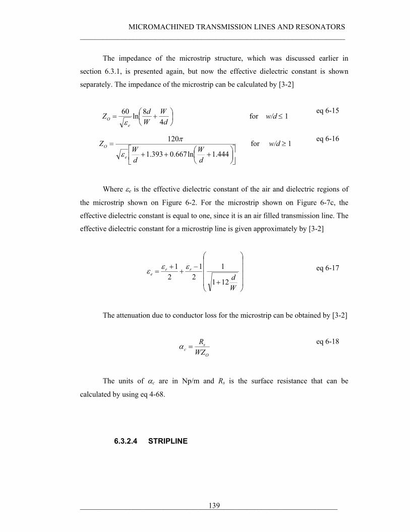
MICROMACHINED TRANSMISSION LINES AND RESONATORS ______________________________________________________________________
____________________________________________________________________ 139
The impedance of the microstrip structure, which was discussed earlier in
section 6.3.1, is presented again, but now the effective dielectric constant is shown
separately. The impedance of the microstrip can be calculated by [3-2]
⎟⎠⎞
⎜⎝⎛ +=
dW
WdZ
eO 4
8ln60ε
for w/d ≤ 1 eq 6-15
⎥⎦
⎤⎢⎣
⎡⎟⎠⎞
⎜⎝⎛ +++
=444.1ln667.0393.1
120
dW
dW
Z
e
O
ε
π for w/d ≥ 1 eq 6-16
Where εe is the effective dielectric constant of the air and dielectric regions of
the microstrip shown on Figure 6-2. For the microstrip shown on Figure 6-7c, the
effective dielectric constant is equal to one, since it is an air filled transmission line. The
effective dielectric constant for a microstrip line is given approximately by [3-2]
⎟⎟⎟⎟
⎠
⎞
⎜⎜⎜⎜
⎝
⎛
+
−+
+=
Wd
rre
121
12
12
1 εεε
eq 6-17
The attenuation due to conductor loss for the microstrip can be obtained by [3-2]
O
sc WZ
R=α
eq 6-18
The units of αc are in Np/m and Rs is the surface resistance that can be
calculated by using eq 4-68.
6.3.2.4 STRIPLINE
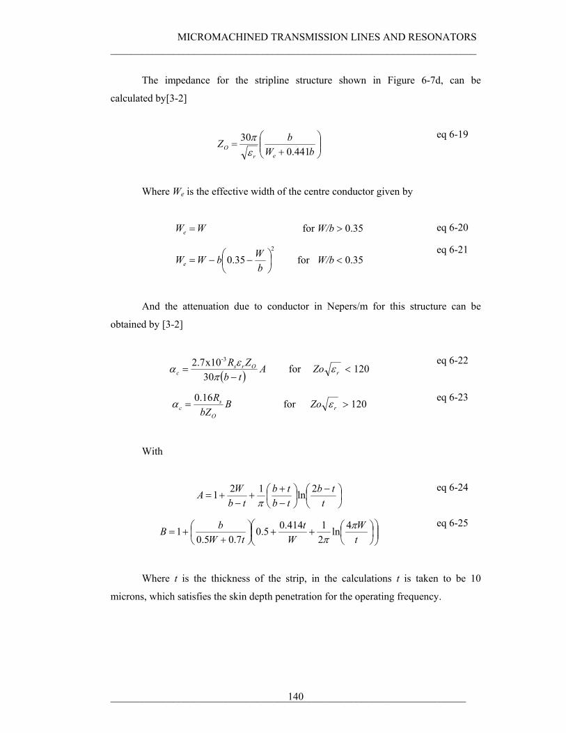
MICROMACHINED TRANSMISSION LINES AND RESONATORS ______________________________________________________________________
____________________________________________________________________ 140
The impedance for the stripline structure shown in Figure 6-7d, can be
calculated by[3-2]
⎟⎟⎠
⎞⎜⎜⎝
⎛+
=bW
bZer
O 441.030επ
eq 6-19
Where We is the effective width of the centre conductor given by
WWe = for W/b > 0.35 eq 6-20
2
35.0 ⎟⎠⎞
⎜⎝⎛ −−=
bWbWWe for W/b < 0.35
eq 6-21
And the attenuation due to conductor in Nepers/m for this structure can be
obtained by [3-2]
( ) Atb
ZR Orsc −=
πεα
30x107.2 -3
for rZo ε < 120 eq 6-22
BbZ
RO
sc
16.0=α for rZo ε > 120
eq 6-23
With
⎟⎠⎞
⎜⎝⎛ −
⎟⎠⎞
⎜⎝⎛
−+
+−
+=t
tbtbtb
tbWA 2ln121
π
eq 6-24
⎟⎟⎠
⎞⎜⎜⎝
⎛⎟⎠⎞
⎜⎝⎛++⎟
⎠⎞
⎜⎝⎛
++=
tW
Wt
tWbB π
π4ln
21414.05.0
7.05.01
eq 6-25
Where t is the thickness of the strip, in the calculations t is taken to be 10
microns, which satisfies the skin depth penetration for the operating frequency.
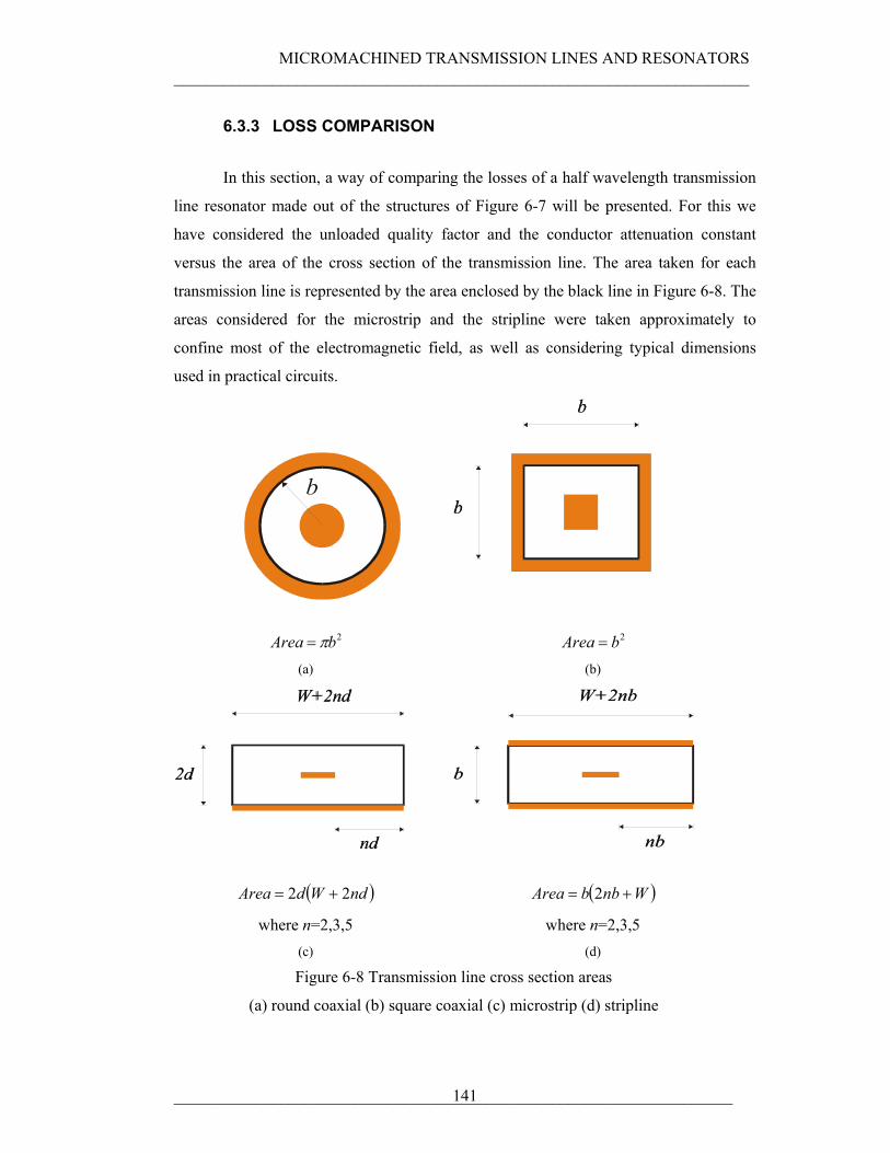
MICROMACHINED TRANSMISSION LINES AND RESONATORS ______________________________________________________________________
____________________________________________________________________ 141
6.3.3 LOSS COMPARISON
In this section, a way of comparing the losses of a half wavelength transmission
line resonator made out of the structures of Figure 6-7 will be presented. For this we
have considered the unloaded quality factor and the conductor attenuation constant
versus the area of the cross section of the transmission line. The area taken for each
transmission line is represented by the area enclosed by the black line in Figure 6-8. The
areas considered for the microstrip and the stripline were taken approximately to
confine most of the electromagnetic field, as well as considering typical dimensions
used in practical circuits.
b
b
b
2bArea π= (a)
2bArea = (b)
nd
2d
W+2nd
b
W+2nb
nb
( )ndWdArea 22 +=
where n=2,3,5 (c)
( )WnbbArea += 2
where n=2,3,5 (d)
Figure 6-8 Transmission line cross section areas
(a) round coaxial (b) square coaxial (c) microstrip (d) stripline
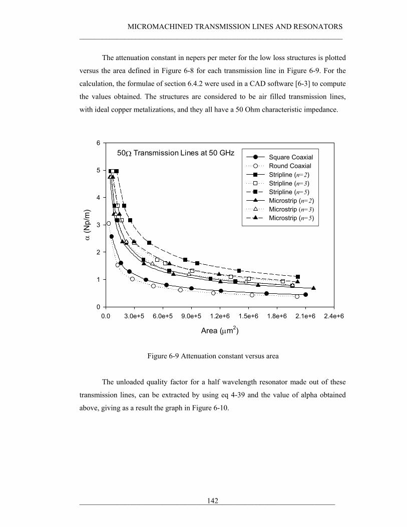
MICROMACHINED TRANSMISSION LINES AND RESONATORS ______________________________________________________________________
____________________________________________________________________ 142
The attenuation constant in nepers per meter for the low loss structures is plotted
versus the area defined in Figure 6-8 for each transmission line in Figure 6-9. For the
calculation, the formulae of section 6.4.2 were used in a CAD software [6-3] to compute
the values obtained. The structures are considered to be air filled transmission lines,
with ideal copper metalizations, and they all have a 50 Ohm characteristic impedance.
Area (µm2)
0.0 3.0e+5 6.0e+5 9.0e+5 1.2e+6 1.5e+6 1.8e+6 2.1e+6 2.4e+6
α (N
p/m
)
0
1
2
3
4
5
6
Square CoaxialRound CoaxialStripline (n=2)Stripline (n=3)Stripline (n=5)Microstrip (n=2)Microstrip (n=3)Microstrip (n=5)
50Ω Transmission Lines at 50 GHz
Figure 6-9 Attenuation constant versus area
The unloaded quality factor for a half wavelength resonator made out of these
transmission lines, can be extracted by using eq 4-39 and the value of alpha obtained
above, giving as a result the graph in Figure 6-10.
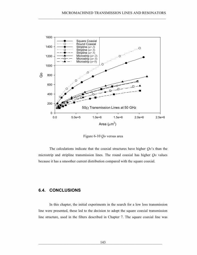
MICROMACHINED TRANSMISSION LINES AND RESONATORS ______________________________________________________________________
____________________________________________________________________ 143
Area (µm2)
0.0 5.0e+5 1.0e+6 1.5e+6 2.0e+6 2.5e+6
Qo
0
200
400
600
800
1000
1200
1400
1600Square CoaxialRound CoaxialStripline (n=2)Stripline (n=3)Stripline (n=5)Microstrip (n=2)Microstrip (n=3)Microstrip (n=5)
50Ω Transmission Lines at 50 GHz
Figure 6-10 Qo versus area
The calculations indicate that the coaxial structures have higher Qo’s than the
microstrip and stripline transmission lines. The round coaxial has higher Qo values
because it has a smoother current distribution compared with the square coaxial.
6.4. CONCLUSIONS
In this chapter, the initial experiments in the search for a low loss transmission
line were presented, these led to the decision to adopt the square coaxial transmission
line structure, used in the filters described in Chapter 7. The square coaxial line was
MICROMACHINED TRANSMISSION LINES AND RESONATORS ______________________________________________________________________
____________________________________________________________________ 144
chosen over the round coaxial line, because stacking thick planar layers of material
allow an easier manufacturing process compared to the round coaxial.
Finally a conductor loss comparison of different low loss transmission lines was
done analytically, with the objective of showing the advantages of using a square
coaxial transmission line.
6.5. REFERENCES
[3-2] D.M. Pozar
[6-1] Brian C. Wadell, “Transmission line design handbook” Artech House, Inc., 1991
[4-10] HFSS [3-5] P.A. Rizzi,
[6-2] K.H.Lau, “Loss calculations for rectangular coaxial lines” IEE proceedings,
Vol. 135, pt. H, No. 3, pp. 207-209, June 1988
[6-3] Mathcad 8 professional by Mathsoft Inc.
I.Llamas-Garro, PhD thesis (2003), The University of Birmingham, UK
7. CHAPTER SEVEN
SQUARE COAXIAL MICROWAVE BANDPASS FILTERS
7.1. INTRODUCTION
This chapter will be divided into two parts. Part I contains a description of
filters, which were designed using a coaxial structure, which has its centre conductor
supported with a bar of dielectric. Part II describes filters, which were designed out of
all-metal structures that have an air propagation media, enhancing filter performance by
avoiding substrate losses.
Each section details how the design parameters were calculated, and also
includes the technical drawings of the pieces that compose the filter. All the filters
presented in this chapter have a Chebycheff response, and all simulated results
presented are assumed to have perfect conductors.
SQUARE COAXIAL MICROWAVE FILTERS ______________________________________________________________________
____________________________________________________________________ 146
PART I. DIELECTRIC SUPPORTED FILTERS
7.2. X BAND NARROW BAND FILTER
The filter discussed in this section is a three pole, 1% fractional bandwidth band
pass filter with a centre frequency of 9 GHz, with a pass band ripple of 0.01 dB. The
filter is formed by using a square coaxial transmission line with its centre conductor
supported on a bar of dielectric. The dielectric used is PTFE with the same properties as
the one used in the square coaxial resonator discussed in Chapter 6, section 6.2.4. The
filter uses half wavelength resonators, and the filter design parameters are shown in
Table 7-1.
g1= 0.6291 g2= 0.9702
Qe= 62.91 kc= 0.013
Table 7-1 Design parameters for the narrow band X band filter
7.2.1. DESIGN PARAMETERS
In this section, the method of finding the external quality factor and the coupling
coefficients will be addressed; this section uses the techniques discussed in Chapter 5,
section 5.3.3 to extract the values of the external quality factor, and the coupling
coefficients involved with this particular design. To find the external quality factor, the
set up illustrated in Figure 7-1 is used in a 3D electromagnetic CAD simulator [4-10].
SQUARE COAXIAL MICROWAVE FILTERS ______________________________________________________________________
____________________________________________________________________ 147
Weak coupling
X
port
PTFE
Port
Resonator
Feed Feed
(a)
Air
PTFE (b)
Figure 7-1 Extracting Qe for the narrowband X-band filter (a) side view, (b) end view
The distance X in Figure 7-1a is varied, and the external quality factor is
calculated for each distance. The external quality factor for various values of X is
plotted in Figure 7-2.
SQUARE COAXIAL MICROWAVE FILTERS ______________________________________________________________________
____________________________________________________________________ 148
X (mm)
0.5 1.0 1.5 2.0 2.5 3.0 3.5 4.0 4.5
Qe
0
20
40
60
80
100
120
140
160
180
Figure 7-2 Qe for the narrowband X-band filter
To calculate the couplings between resonators, the set up in Figure 7-3 is used in
a 3D electromagnetic CAD simulator [4-10]
YPort
Port
PTFE
Resonator 2
Wall
Resonator 1Gap
Feed
Weak coupling
Feed
Air
Figure 7-3 Extracting kc for the narrowband X-band filter (top view)
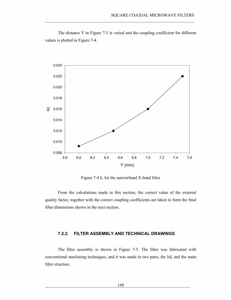
SQUARE COAXIAL MICROWAVE FILTERS ______________________________________________________________________
____________________________________________________________________ 149
The distance Y in Figure 7-3 is varied and the coupling coefficient for different
values is plotted in Figure 7-4.
Y (mm)
5.8 6.0 6.2 6.4 6.6 6.8 7.0 7.2 7.4 7.6
kc
0.008
0.010
0.012
0.014
0.016
0.018
0.020
0.022
0.024
Figure 7-4 kc for the narrowband X-band filter
From the calculations made in this section, the correct value of the external
quality factor, together with the correct coupling coefficients are taken to form the final
filter dimensions shown in the next section.
7.2.2. FILTER ASSEMBLY AND TECHNICAL DRAWINGS
The filter assembly is shown in Figure 7-5. The filter was fabricated with
conventional machining techniques, and it was made in two parts, the lid, and the main
filter structure.
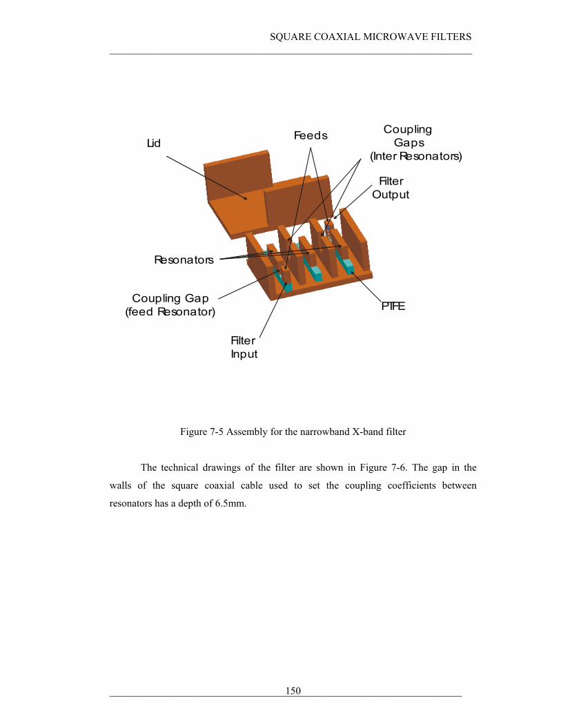
SQUARE COAXIAL MICROWAVE FILTERS ______________________________________________________________________
____________________________________________________________________ 150
FilterOutput
FilterInput
PTFE
Feeds
Resonators
Lid Coupling Gaps (Inter Resonators)
Coupling Gap(feed Resonator)
Figure 7-5 Assembly for the narrowband X-band filter
The technical drawings of the filter are shown in Figure 7-6. The gap in the
walls of the square coaxial cable used to set the coupling coefficients between
resonators has a depth of 6.5mm.
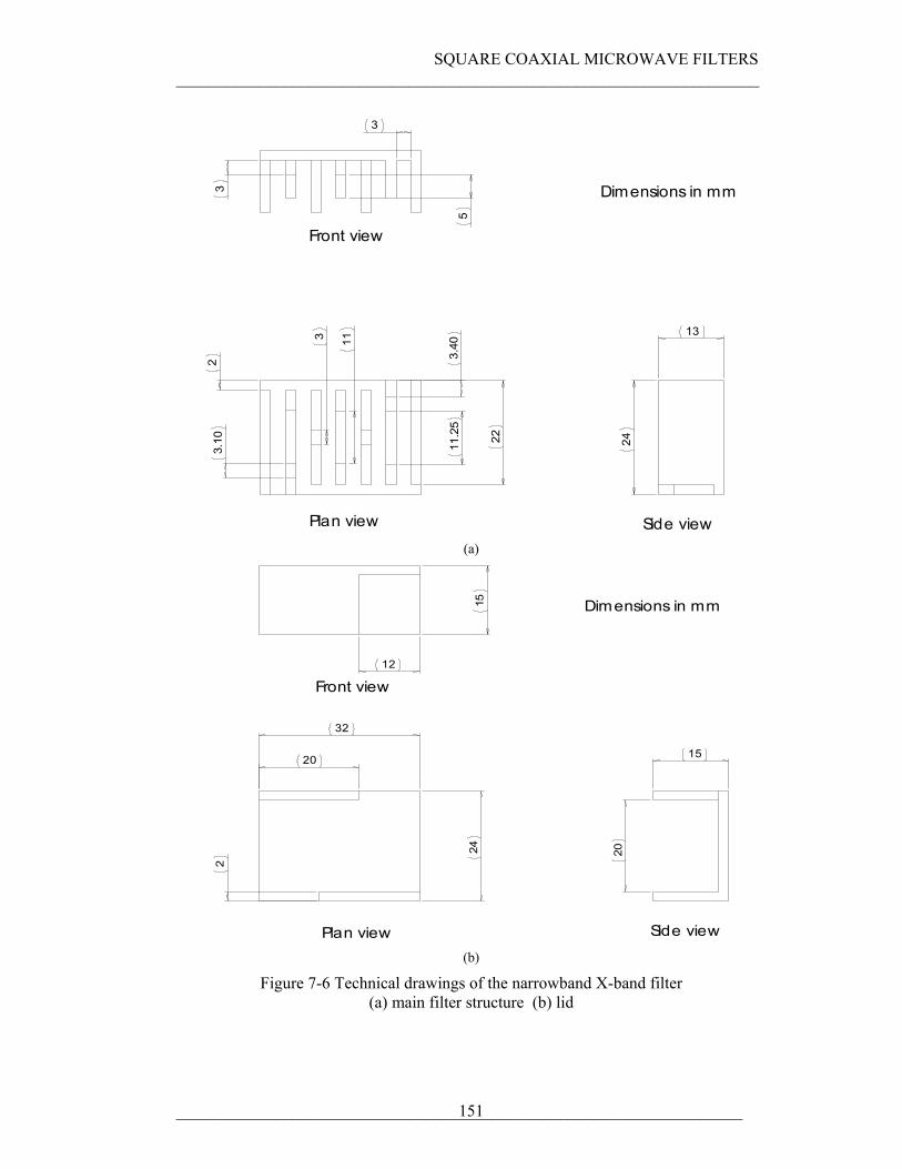
SQUARE COAXIAL MICROWAVE FILTERS ______________________________________________________________________
____________________________________________________________________ 151
2211.2
53.
40
3.10
113
2
5
3
3
13
24
Dimensions in mm
Plan view
Front view
Side view (a)
32
20
24
2
12
15
20
15
Dimensions in mm
Plan view
Front view
Side view (b)
Figure 7-6 Technical drawings of the narrowband X-band filter (a) main filter structure (b) lid
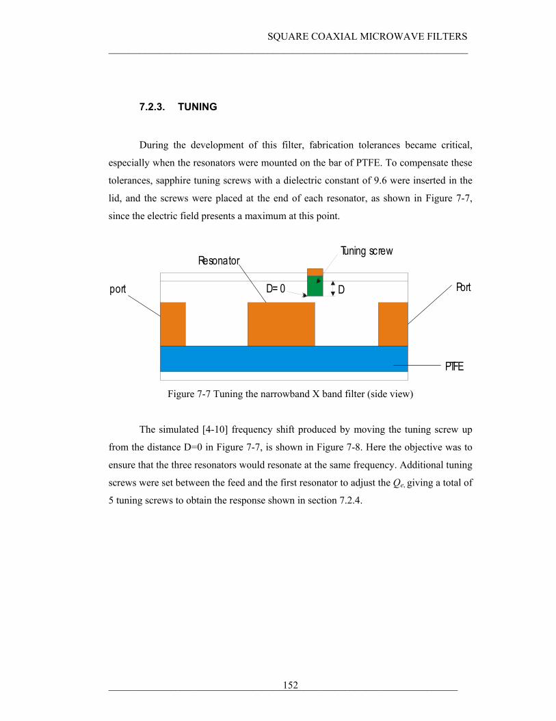
SQUARE COAXIAL MICROWAVE FILTERS ______________________________________________________________________
____________________________________________________________________ 152
7.2.3. TUNING
During the development of this filter, fabrication tolerances became critical,
especially when the resonators were mounted on the bar of PTFE. To compensate these
tolerances, sapphire tuning screws with a dielectric constant of 9.6 were inserted in the
lid, and the screws were placed at the end of each resonator, as shown in Figure 7-7,
since the electric field presents a maximum at this point.
port
PTFE
Port
Resonator
DD= 0
Tuning screw
Figure 7-7 Tuning the narrowband X band filter (side view)
The simulated [4-10] frequency shift produced by moving the tuning screw up
from the distance D=0 in Figure 7-7, is shown in Figure 7-8. Here the objective was to
ensure that the three resonators would resonate at the same frequency. Additional tuning
screws were set between the feed and the first resonator to adjust the Qe, giving a total of
5 tuning screws to obtain the response shown in section 7.2.4.
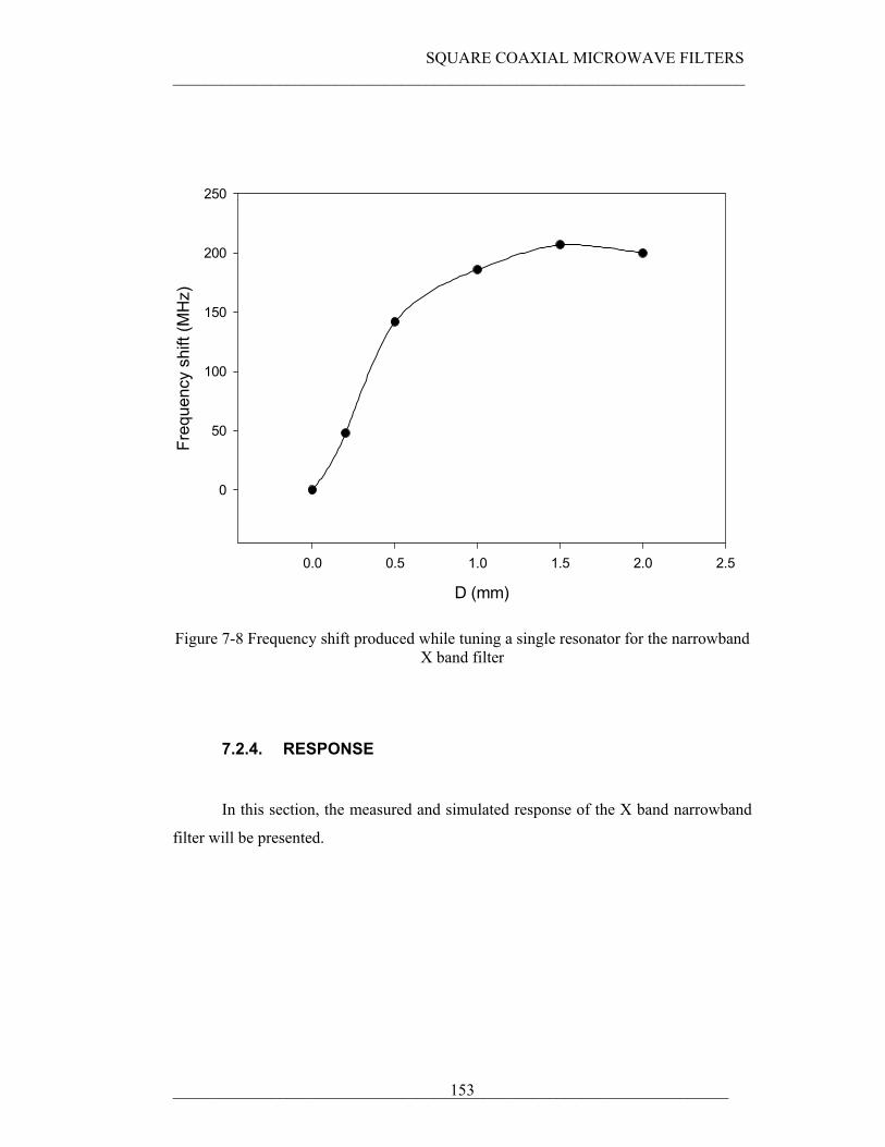
SQUARE COAXIAL MICROWAVE FILTERS ______________________________________________________________________
____________________________________________________________________ 153
D (mm)
0.0 0.5 1.0 1.5 2.0 2.5
Freq
uenc
y sh
ift (M
Hz)
0
50
100
150
200
250
Figure 7-8 Frequency shift produced while tuning a single resonator for the narrowband X band filter
7.2.4. RESPONSE
In this section, the measured and simulated response of the X band narrowband
filter will be presented.
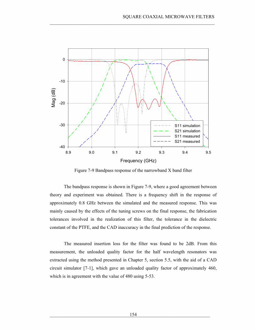
SQUARE COAXIAL MICROWAVE FILTERS ______________________________________________________________________
____________________________________________________________________ 154
Frequency (GHz)
8.9 9.0 9.1 9.2 9.3 9.4 9.5
Mag
(dB)
-40
-30
-20
-10
0
S11 simulationS21 simulationS11 measuredS21 measured
Figure 7-9 Bandpass response of the narrowband X band filter
The bandpass response is shown in Figure 7-9, where a good agreement between
theory and experiment was obtained. There is a frequency shift in the response of
approximately 0.8 GHz between the simulated and the measured response. This was
mainly caused by the effects of the tuning screws on the final response, the fabrication
tolerances involved in the realization of this filter, the tolerance in the dielectric
constant of the PTFE, and the CAD inaccuracy in the final prediction of the response.
The measured insertion loss for the filter was found to be 2dB. From this
measurement, the unloaded quality factor for the half wavelength resonators was
extracted using the method presented in Chapter 5, section 5.5, with the aid of a CAD
circuit simulator [7-1], which gave an unloaded quality factor of approximately 460,
which is in agreement with the value of 480 using 5-53.
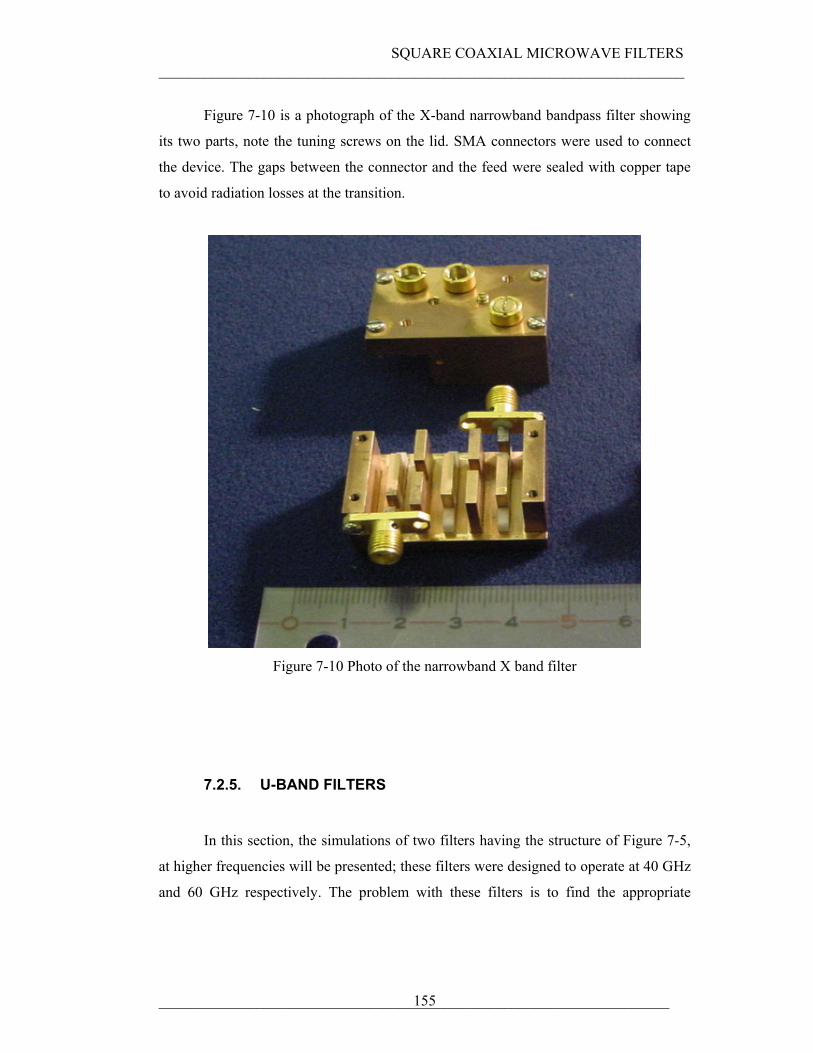
SQUARE COAXIAL MICROWAVE FILTERS ______________________________________________________________________
____________________________________________________________________ 155
Figure 7-10 is a photograph of the X-band narrowband bandpass filter showing
its two parts, note the tuning screws on the lid. SMA connectors were used to connect
the device. The gaps between the connector and the feed were sealed with copper tape
to avoid radiation losses at the transition.
Figure 7-10 Photo of the narrowband X band filter
7.2.5. U-BAND FILTERS
In this section, the simulations of two filters having the structure of Figure 7-5,
at higher frequencies will be presented; these filters were designed to operate at 40 GHz
and 60 GHz respectively. The problem with these filters is to find the appropriate
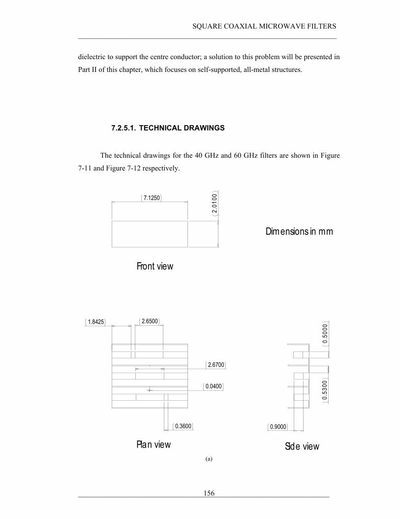
SQUARE COAXIAL MICROWAVE FILTERS ______________________________________________________________________
____________________________________________________________________ 156
dielectric to support the centre conductor; a solution to this problem will be presented in
Part II of this chapter, which focuses on self-supported, all-metal structures.
7.2.5.1. TECHNICAL DRAWINGS
The technical drawings for the 40 GHz and 60 GHz filters are shown in Figure
7-11 and Figure 7-12 respectively.
2.65001.8425
0.3600
0.0400
2.6700
7.1250
2.01
00
0.50
00
0.9000
0.53
00
Dimensions in mm
Plan view Side view
Front view
(a)
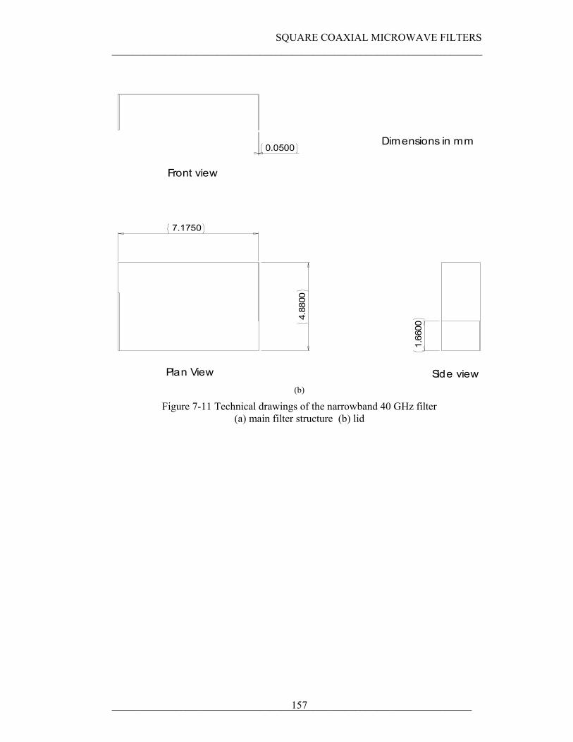
SQUARE COAXIAL MICROWAVE FILTERS ______________________________________________________________________
____________________________________________________________________ 157
7.1750
4.88
00
0.0500
1.66
00
Dimensions in mm
Plan View Side view
Front view
(b)
Figure 7-11 Technical drawings of the narrowband 40 GHz filter (a) main filter structure (b) lid
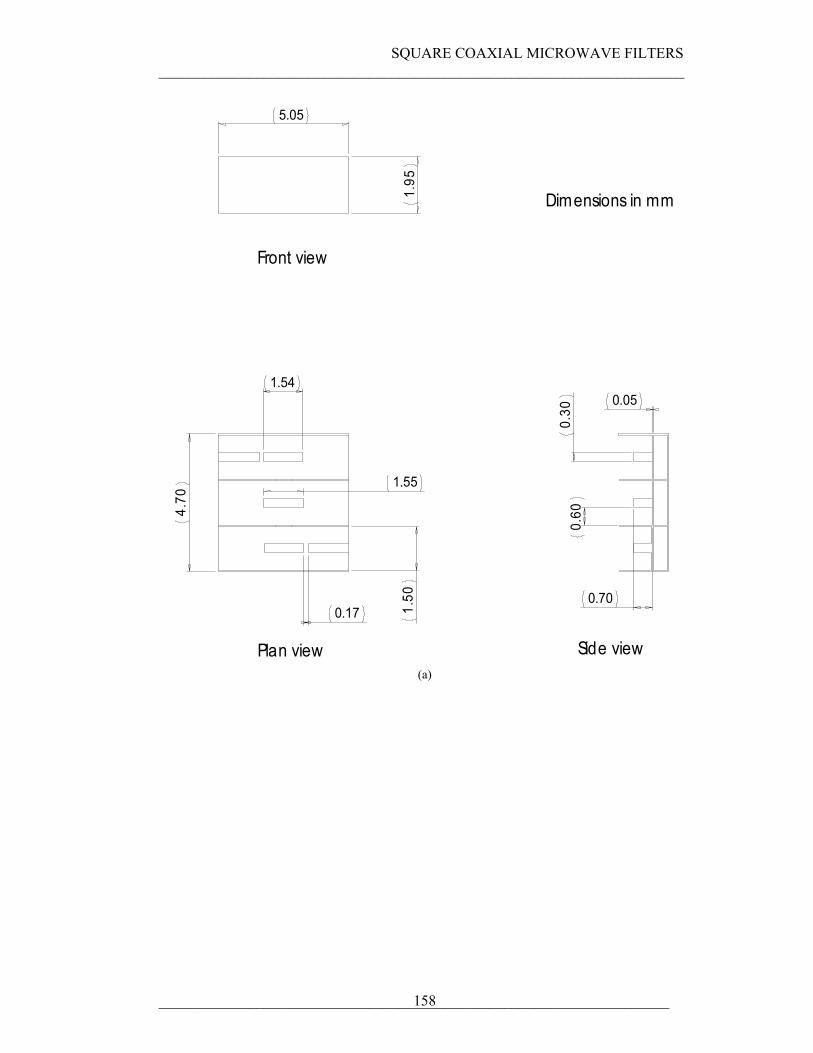
SQUARE COAXIAL MICROWAVE FILTERS ______________________________________________________________________
____________________________________________________________________ 158
1.54
0.17
1.55
4.70
1.50
5.05
1.95
0.30
0.05
0.60
0.70
Dimensions in mm
Plan view Side view
Front view
(a)
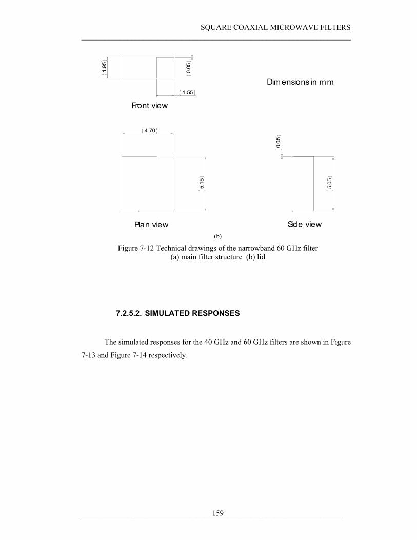
SQUARE COAXIAL MICROWAVE FILTERS ______________________________________________________________________
____________________________________________________________________ 159
5.15
4.70
1.55
0.05
1.95
0.05
5.05
Dimensions in mm
Plan view Side view
Front view
(b)
Figure 7-12 Technical drawings of the narrowband 60 GHz filter (a) main filter structure (b) lid
7.2.5.2. SIMULATED RESPONSES
The simulated responses for the 40 GHz and 60 GHz filters are shown in Figure
7-13 and Figure 7-14 respectively.
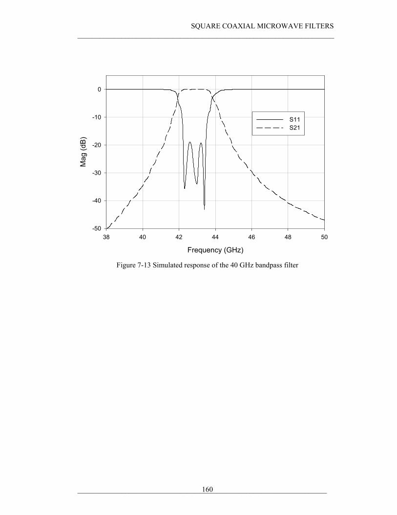
SQUARE COAXIAL MICROWAVE FILTERS ______________________________________________________________________
____________________________________________________________________ 160
Frequency (GHz)
38 40 42 44 46 48 50
Mag
(dB)
-50
-40
-30
-20
-10
0
S11S21
Figure 7-13 Simulated response of the 40 GHz bandpass filter
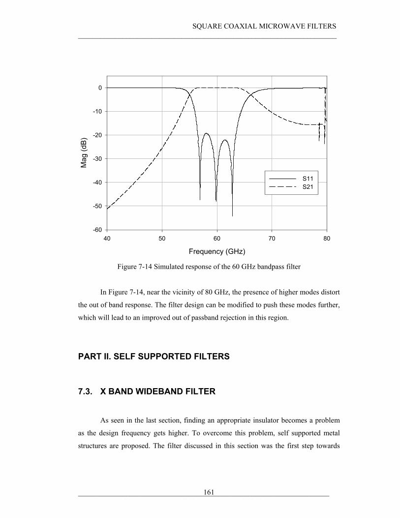
SQUARE COAXIAL MICROWAVE FILTERS ______________________________________________________________________
____________________________________________________________________ 161
Frequency (GHz)
40 50 60 70 80
Mag
(dB)
-60
-50
-40
-30
-20
-10
0
S11S21
Figure 7-14 Simulated response of the 60 GHz bandpass filter
In Figure 7-14, near the vicinity of 80 GHz, the presence of higher modes distort
the out of band response. The filter design can be modified to push these modes further,
which will lead to an improved out of passband rejection in this region.
PART II. SELF SUPPORTED FILTERS
7.3. X BAND WIDEBAND FILTER
As seen in the last section, finding an appropriate insulator becomes a problem
as the design frequency gets higher. To overcome this problem, self supported metal
structures are proposed. The filter discussed in this section was the first step towards
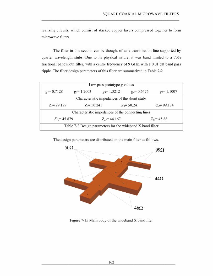
SQUARE COAXIAL MICROWAVE FILTERS ______________________________________________________________________
____________________________________________________________________ 162
realizing circuits, which consist of stacked copper layers compressed together to form
microwave filters.
The filter in this section can be thought of as a transmission line supported by
quarter wavelength stubs. Due to its physical nature, it was band limited to a 70%
fractional bandwidth filter, with a centre frequency of 9 GHz, with a 0.01 dB band pass
ripple. The filter design parameters of this filter are summarized in Table 7-2.
Low pass prototype g values
g1= 0.7128 g2= 1.2003 g3= 1.3212 g4= 0.6476 g5= 1.1007
Characteristic impedances of the shunt stubs
Z1= 99.179 Z2= 50.241 Z3= 50.24 Z4= 99.174
Characteristic impedances of the connecting lines
Z12= 45.879 Z23= 44.167 Z34= 45.88
Table 7-2 Design parameters for the wideband X band filter
The design parameters are distributed on the main filter as follows.
50Ω 99Ω
46Ω
44Ω
Figure 7-15 Main body of the wideband X band fiter
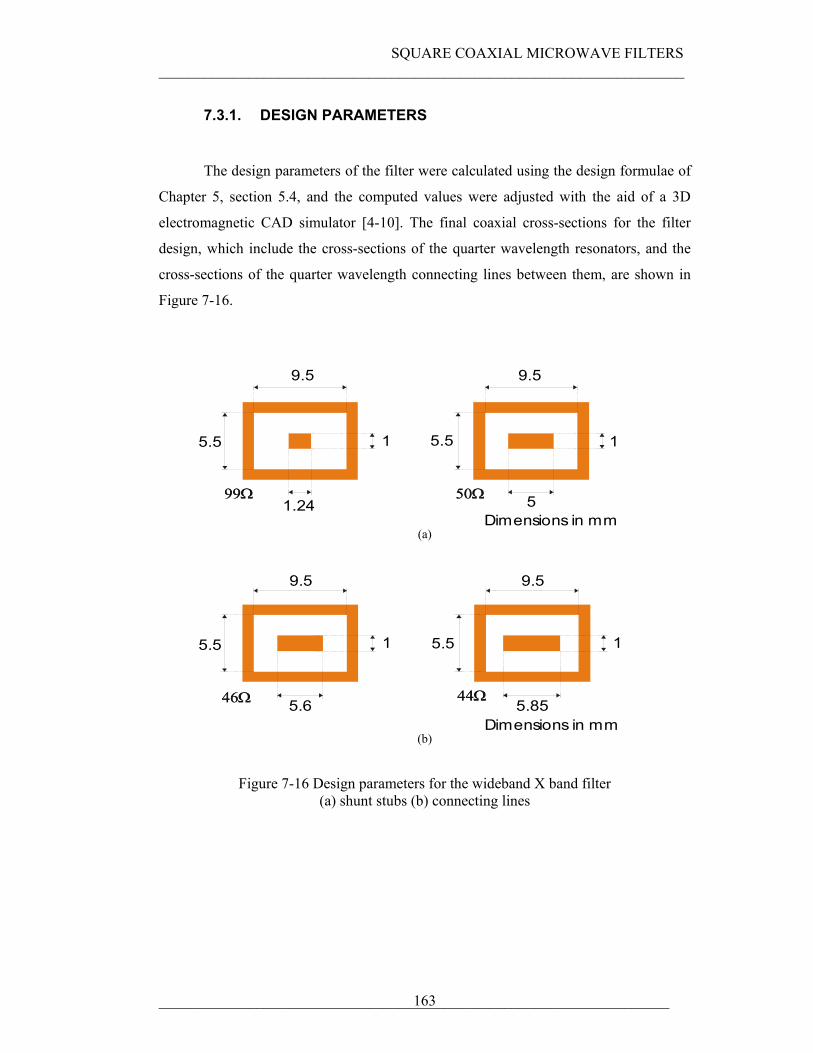
SQUARE COAXIAL MICROWAVE FILTERS ______________________________________________________________________
____________________________________________________________________ 163
7.3.1. DESIGN PARAMETERS
The design parameters of the filter were calculated using the design formulae of
Chapter 5, section 5.4, and the computed values were adjusted with the aid of a 3D
electromagnetic CAD simulator [4-10]. The final coaxial cross-sections for the filter
design, which include the cross-sections of the quarter wavelength resonators, and the
cross-sections of the quarter wavelength connecting lines between them, are shown in
Figure 7-16.
99Ω 50Ω 1.24
9.5
5.5 1
5
1
9.5
5.5
Dimensions in mm(a)
46Ω 44Ω
1
5.6
9.5
5.5 1
5.85
9.5
5.5
Dimensions in mm(b)
Figure 7-16 Design parameters for the wideband X band filter (a) shunt stubs (b) connecting lines
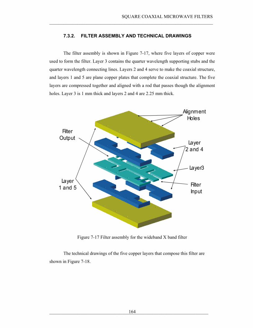
SQUARE COAXIAL MICROWAVE FILTERS ______________________________________________________________________
____________________________________________________________________ 164
7.3.2. FILTER ASSEMBLY AND TECHNICAL DRAWINGS
The filter assembly is shown in Figure 7-17, where five layers of copper were
used to form the filter. Layer 3 contains the quarter wavelength supporting stubs and the
quarter wavelength connecting lines. Layers 2 and 4 serve to make the coaxial structure,
and layers 1 and 5 are plane copper plates that complete the coaxial structure. The five
layers are compressed together and aligned with a rod that passes though the alignment
holes. Layer 3 is 1 mm thick and layers 2 and 4 are 2.25 mm thick.
FilterInput
FilterOutput
Layer3
Layer2 and 4
Layer1 and 5
Alignment Holes
Figure 7-17 Filter assembly for the wideband X band filter
The technical drawings of the five copper layers that compose this filter are
shown in Figure 7-18.
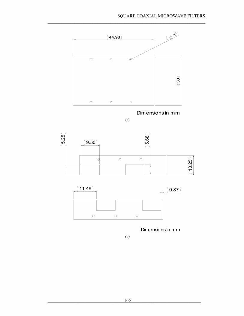
SQUARE COAXIAL MICROWAVE FILTERS ______________________________________________________________________
____________________________________________________________________ 165
44.98
30
1
Dimensions in mm (a)
10.2
5
5.25
9.50 5.68
0.8711.49
Dimensions in mm (b)
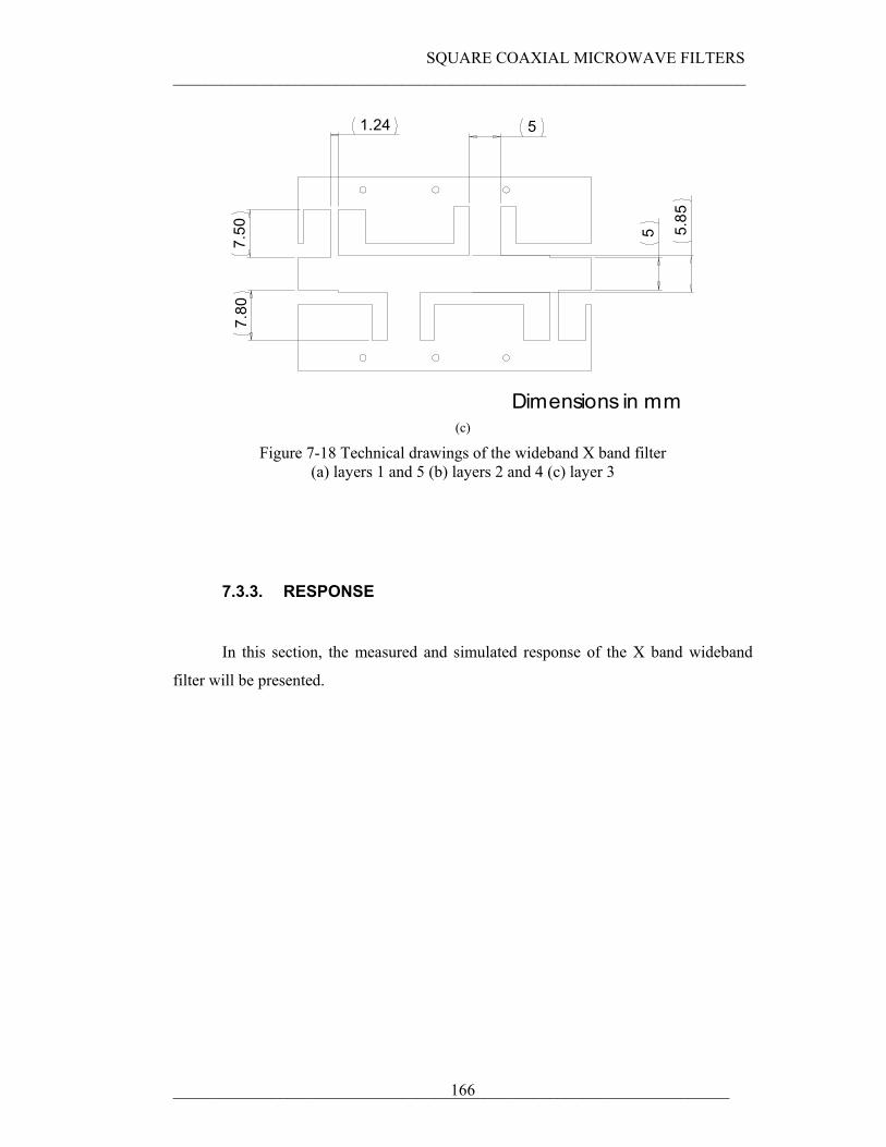
SQUARE COAXIAL MICROWAVE FILTERS ______________________________________________________________________
____________________________________________________________________ 166
51.24
5 5.85
7.50
7.80
Dimensions in mm (c)
Figure 7-18 Technical drawings of the wideband X band filter (a) layers 1 and 5 (b) layers 2 and 4 (c) layer 3
7.3.3. RESPONSE
In this section, the measured and simulated response of the X band wideband
filter will be presented.
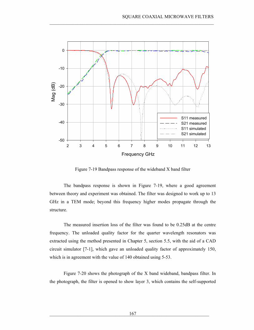
SQUARE COAXIAL MICROWAVE FILTERS ______________________________________________________________________
____________________________________________________________________ 167
Frequency GHz
2 3 4 5 6 7 8 9 10 11 12 13
Mag
(dB
)
-50
-40
-30
-20
-10
0
S11 measuredS21 measuredS11 simulatedS21 simulated
Figure 7-19 Bandpass response of the wideband X band filter
The bandpass response is shown in Figure 7-19, where a good agreement
between theory and experiment was obtained. The filter was designed to work up to 13
GHz in a TEM mode; beyond this frequency higher modes propagate through the
structure.
The measured insertion loss of the filter was found to be 0.25dB at the centre
frequency. The unloaded quality factor for the quarter wavelength resonators was
extracted using the method presented in Chapter 5, section 5.5, with the aid of a CAD
circuit simulator [7-1], which gave an unloaded quality factor of approximately 150,
which is in agreement with the value of 140 obtained using 5-53.
Figure 7-20 shows the photograph of the X band wideband, bandpass filter. In
the photograph, the filter is opened to show layer 3, which contains the self-supported
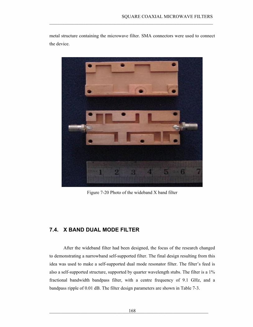
SQUARE COAXIAL MICROWAVE FILTERS ______________________________________________________________________
____________________________________________________________________ 168
metal structure containing the microwave filter. SMA connectors were used to connect
the device.
Figure 7-20 Photo of the wideband X band filter
7.4. X BAND DUAL MODE FILTER
After the wideband filter had been designed, the focus of the research changed
to demonstrating a narrowband self-supported filter. The final design resulting from this
idea was used to make a self-supported dual mode resonator filter. The filter’s feed is
also a self-supported structure, supported by quarter wavelength stubs. The filter is a 1%
fractional bandwidth bandpass filter, with a centre frequency of 9.1 GHz, and a
bandpass ripple of 0.01 dB. The filter design parameters are shown in Table 7-3.
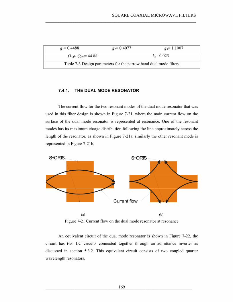
SQUARE COAXIAL MICROWAVE FILTERS ______________________________________________________________________
____________________________________________________________________ 169
g1= 0.4488 g2= 0.4077 g3= 1.1007
QeA≈ QeB = 44.88 kc= 0.023
Table 7-3 Design parameters for the narrow band dual mode filters
7.4.1. THE DUAL MODE RESONATOR
The current flow for the two resonant modes of the dual mode resonator that was
used in this filter design is shown in Figure 7-21, where the main current flow on the
surface of the dual mode resonator is represented at resonance. One of the resonant
modes has its maximum charge distribution following the line approximately across the
length of the resonator, as shown in Figure 7-21a, similarly the other resonant mode is
represented in Figure 7-21b.
SHORTSSHORTS
Current flow
(a) (b)
Figure 7-21 Current flow on the dual mode resonator at resonance
An equivalent circuit of the dual mode resonator is shown in Figure 7-22, the
circuit has two LC circuits connected together through an admittance inverter as
discussed in section 5.3.2. This equivalent circuit consists of two coupled quarter
wavelength resonators.
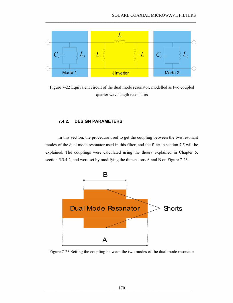
SQUARE COAXIAL MICROWAVE FILTERS ______________________________________________________________________
____________________________________________________________________ 170
L
-L -L L1 L2C2C1
Mode 1 Mode 2J inverter
Figure 7-22 Equivalent circuit of the dual mode resonator, modelled as two coupled
quarter wavelength resonators
7.4.2. DESIGN PARAMETERS
In this section, the procedure used to get the coupling between the two resonant
modes of the dual mode resonator used in this filter, and the filter in section 7.5 will be
explained. The couplings were calculated using the theory explained in Chapter 5,
section 5.3.4.2, and were set by modifying the dimensions A and B on Figure 7-23.
Dual Mode Resonator Shorts
A
B
Figure 7-23 Setting the coupling between the two modes of the dual mode resonator
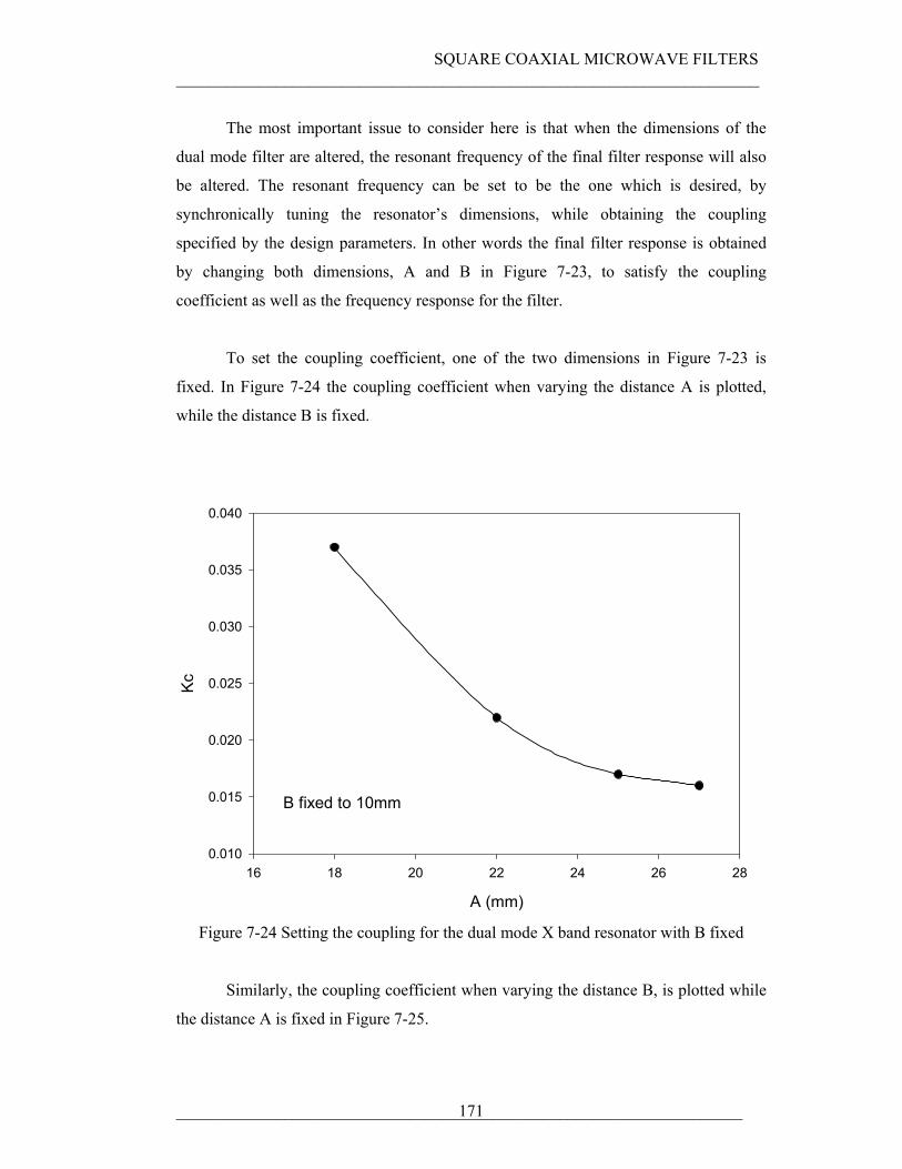
SQUARE COAXIAL MICROWAVE FILTERS ______________________________________________________________________
____________________________________________________________________ 171
The most important issue to consider here is that when the dimensions of the
dual mode filter are altered, the resonant frequency of the final filter response will also
be altered. The resonant frequency can be set to be the one which is desired, by
synchronically tuning the resonator’s dimensions, while obtaining the coupling
specified by the design parameters. In other words the final filter response is obtained
by changing both dimensions, A and B in Figure 7-23, to satisfy the coupling
coefficient as well as the frequency response for the filter.
To set the coupling coefficient, one of the two dimensions in Figure 7-23 is
fixed. In Figure 7-24 the coupling coefficient when varying the distance A is plotted,
while the distance B is fixed.
A (mm)
16 18 20 22 24 26 28
Kc
0.010
0.015
0.020
0.025
0.030
0.035
0.040
B fixed to 10mm
Figure 7-24 Setting the coupling for the dual mode X band resonator with B fixed
Similarly, the coupling coefficient when varying the distance B, is plotted while
the distance A is fixed in Figure 7-25.
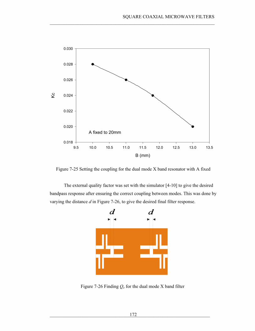
SQUARE COAXIAL MICROWAVE FILTERS ______________________________________________________________________
____________________________________________________________________ 172
A fixed to 20mm
B (mm)
9.5 10.0 10.5 11.0 11.5 12.0 12.5 13.0 13.5
Kc
0.018
0.020
0.022
0.024
0.026
0.028
0.030
Figure 7-25 Setting the coupling for the dual mode X band resonator with A fixed
The external quality factor was set with the simulator [4-10] to give the desired
bandpass response after ensuring the correct coupling between modes. This was done by
varying the distance d in Figure 7-26, to give the desired final filter response.
d d
Figure 7-26 Finding Qe for the dual mode X band filter
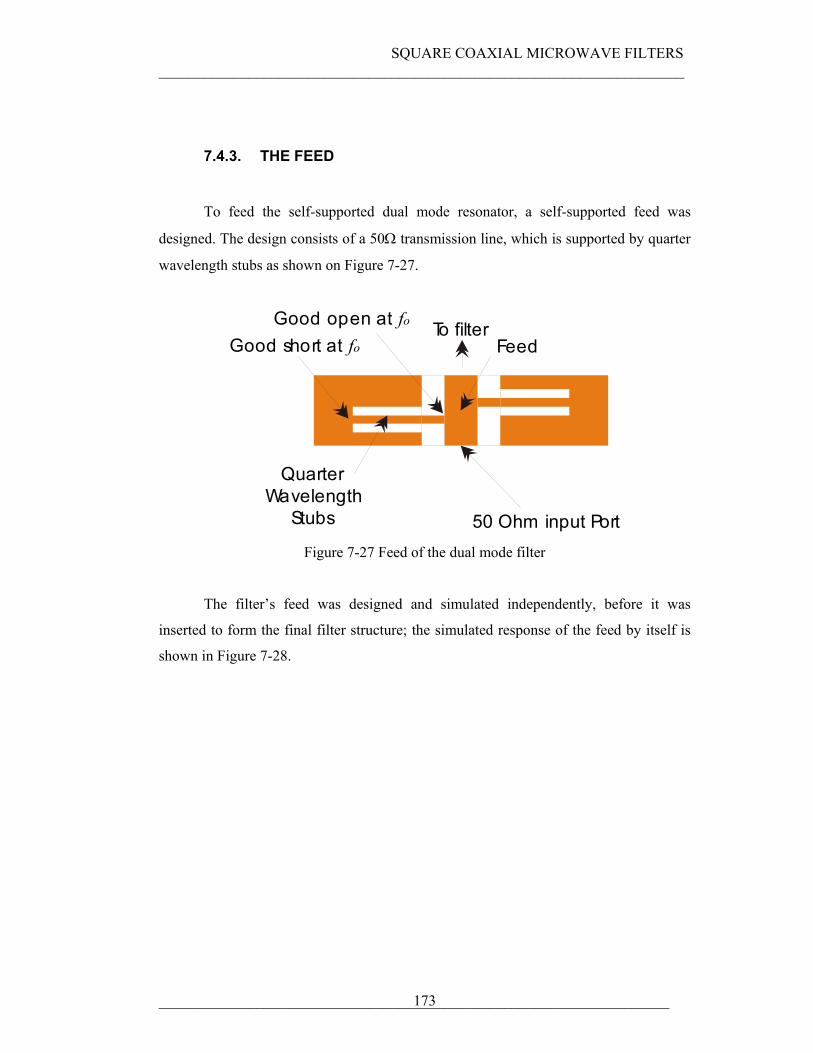
SQUARE COAXIAL MICROWAVE FILTERS ______________________________________________________________________
____________________________________________________________________ 173
7.4.3. THE FEED
To feed the self-supported dual mode resonator, a self-supported feed was
designed. The design consists of a 50Ω transmission line, which is supported by quarter
wavelength stubs as shown on Figure 7-27.
Quarter Wavelength Stubs
Feed
50 Ohm input Port
Good open at foGood short at fo
To filter
Figure 7-27 Feed of the dual mode filter
The filter’s feed was designed and simulated independently, before it was
inserted to form the final filter structure; the simulated response of the feed by itself is
shown in Figure 7-28.
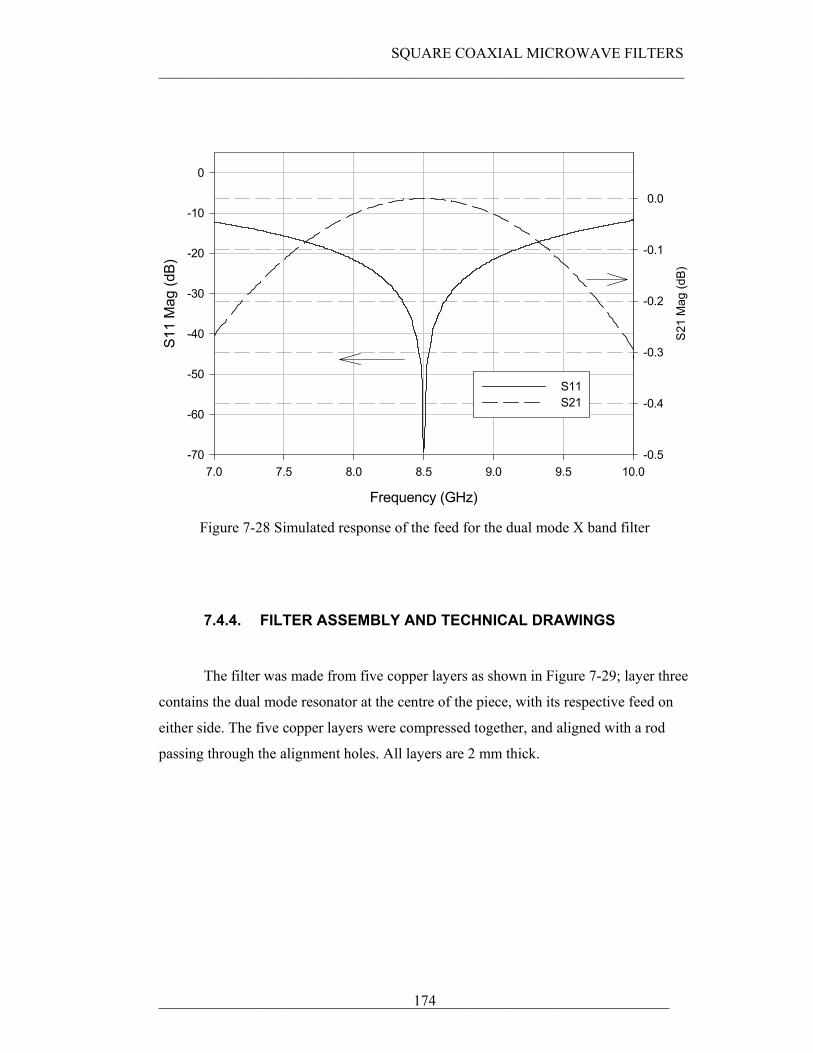
SQUARE COAXIAL MICROWAVE FILTERS ______________________________________________________________________
____________________________________________________________________ 174
Frequency (GHz)
7.0 7.5 8.0 8.5 9.0 9.5 10.0
S11
Mag
(dB)
-70
-60
-50
-40
-30
-20
-10
0
S21
Mag
(dB)
-0.5
-0.4
-0.3
-0.2
-0.1
0.0
S11S21
Figure 7-28 Simulated response of the feed for the dual mode X band filter
7.4.4. FILTER ASSEMBLY AND TECHNICAL DRAWINGS
The filter was made from five copper layers as shown in Figure 7-29; layer three
contains the dual mode resonator at the centre of the piece, with its respective feed on
either side. The five copper layers were compressed together, and aligned with a rod
passing through the alignment holes. All layers are 2 mm thick.
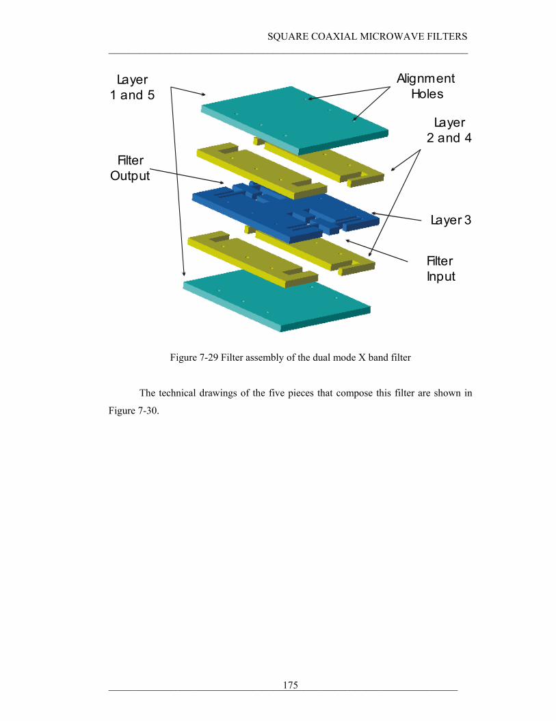
SQUARE COAXIAL MICROWAVE FILTERS ______________________________________________________________________
____________________________________________________________________ 175
Layer 3
Layer1 and 5
Layer2 and 4
FilterInput
FilterOutput
Alignment Holes
Figure 7-29 Filter assembly of the dual mode X band filter
The technical drawings of the five pieces that compose this filter are shown in
Figure 7-30.
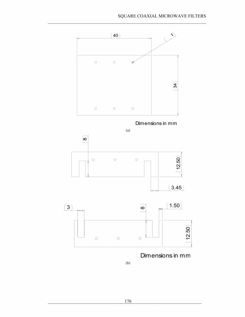
SQUARE COAXIAL MICROWAVE FILTERS ______________________________________________________________________
____________________________________________________________________ 176
40
34
1
Dimensions in mm (a)
3.45
8
12.5
0
1.503
12.5
0
8
Dimensions in mm (b)
SQUARE COAXIAL MICROWAVE FILTERS ______________________________________________________________________
____________________________________________________________________ 177
9.50
20
1
3.75
9
1.85 8.15
Dimensions in mm (c)
Figure 7-30 Technical drawings of the dual mode X band filter (a) layers 1 and 5 (b) layers 2 and 4 (c) layer 3
7.4.5. RESPONSE
In this section, the measured and simulated response of the X band dual mode
filter will be presented.
SQUARE COAXIAL MICROWAVE FILTERS ______________________________________________________________________
____________________________________________________________________ 178
Frequency (GHz)
8.2 8.4 8.6 8.8 9.0 9.2 9.4 9.6 9.8 10.0
Mag
(dB)
-40
-30
-20
-10
0
S11 measuredS21 measuredS11 simulatedS21 simulated
Figure 7-31 Bandpass response of the dual mode X band filter
The bandpass response of the dual mode X-band filter is shown in Figure 7-31,
where a good agreement between theory and experiment was obtained. The measured
insertion loss of the filter was found to be 2.2dB. From this measurement, the unloaded
quality factor for the dual mode resonator was extracted, using the method presented in
Chapter 5, section 5.5, with the aid of a CAD circuit simulator [7-1], which gave an
unloaded quality factor of approximately 190, which is in agreement with the value of
170 obtained using 5-53. The measured bandwidth increased due to layer misalignment,
which changed the coupling between the two modes.
Figure 7-32 shows the photograph of the dual mode X-band bandpass filter; in
the photograph, the filter was opened to show layer 3, which contains the self-supported
metal structure containing the microwave dual mode resonator, with its self-supported
feeds. SMA connectors were used to connect the device.
SQUARE COAXIAL MICROWAVE FILTERS ______________________________________________________________________
____________________________________________________________________ 179
Figure 7-32 Photo of the dual mode X band filter
7.5. KA BAND DUAL MODE MICROMACHINED FILTER
This filter has the same structure as the filter discussed in section 7.4. Here the
filter was designed to satisfy the LMDS specification shown in Table 1-2. The filter
design parameters are summarized in Table 7-3. The filter is a 1% fractional bandwidth
filter, with a centre frequency of 29.75 GHz, and a 0.01dB passband ripple.
SQUARE COAXIAL MICROWAVE FILTERS ______________________________________________________________________
____________________________________________________________________ 180
7.5.1. DESIGN PARAMETERS
The procedure to obtain the coupling coefficient for this filter was explained in
section 7.4.2, referring to Figure 7-23 and the theory described in Chapter 5, section
5.3.3.2. The coupling coefficient when varying the distance A is plotted in Figure 7-33,
while the distance B is fixed.
B is fixed to 3000 microns
A (microns)
6000 6200 6400 6600 6800 7000 7200
Kc
0.016
0.017
0.018
0.019
0.020
0.021
0.022
0.023
0.024
Figure 7-33 Setting the coupling for the dual mode Ka band resonator with B fixed
Similarly, referring to Figure 7-23, the coupling coefficient when varying the
distance B is plotted, while the distance A is fixed in Figure 7-34.
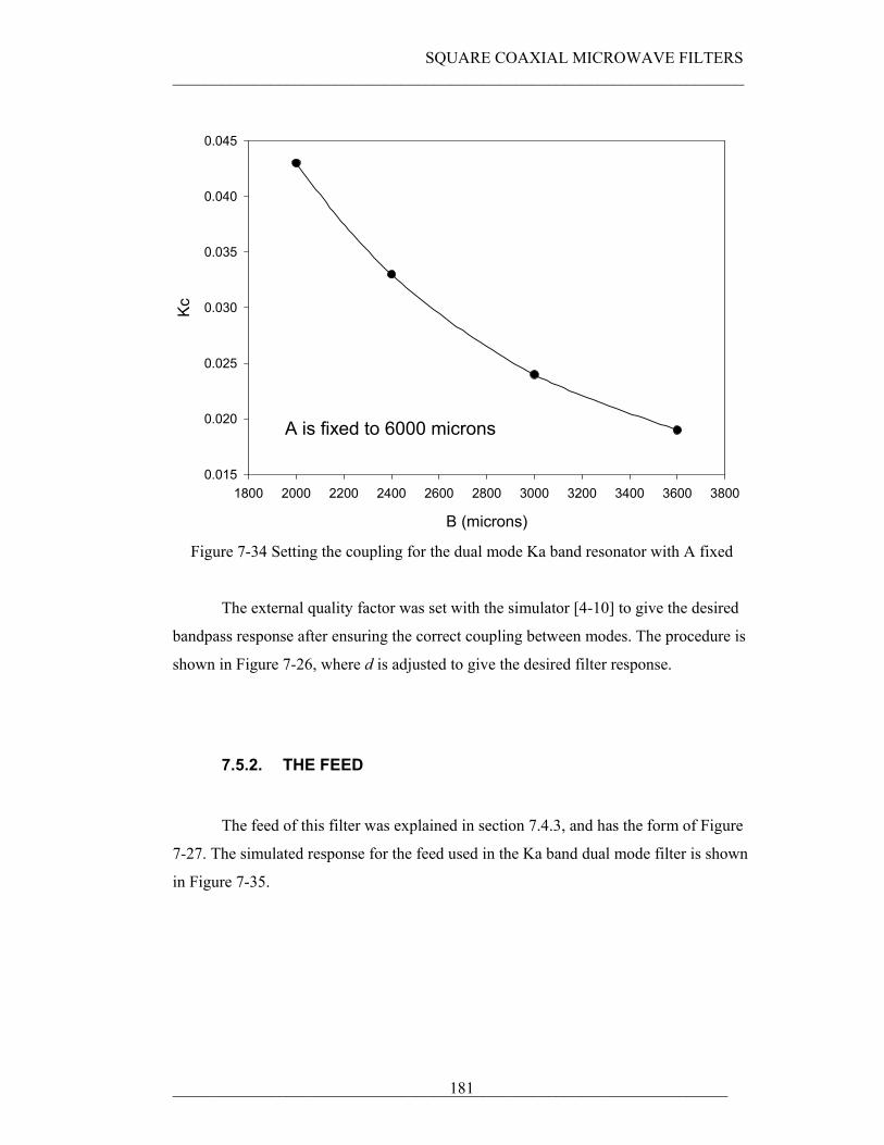
SQUARE COAXIAL MICROWAVE FILTERS ______________________________________________________________________
____________________________________________________________________ 181
A is fixed to 6000 microns
B (microns)
1800 2000 2200 2400 2600 2800 3000 3200 3400 3600 3800
Kc
0.015
0.020
0.025
0.030
0.035
0.040
0.045
Figure 7-34 Setting the coupling for the dual mode Ka band resonator with A fixed
The external quality factor was set with the simulator [4-10] to give the desired
bandpass response after ensuring the correct coupling between modes. The procedure is
shown in Figure 7-26, where d is adjusted to give the desired filter response.
7.5.2. THE FEED
The feed of this filter was explained in section 7.4.3, and has the form of Figure
7-27. The simulated response for the feed used in the Ka band dual mode filter is shown
in Figure 7-35.
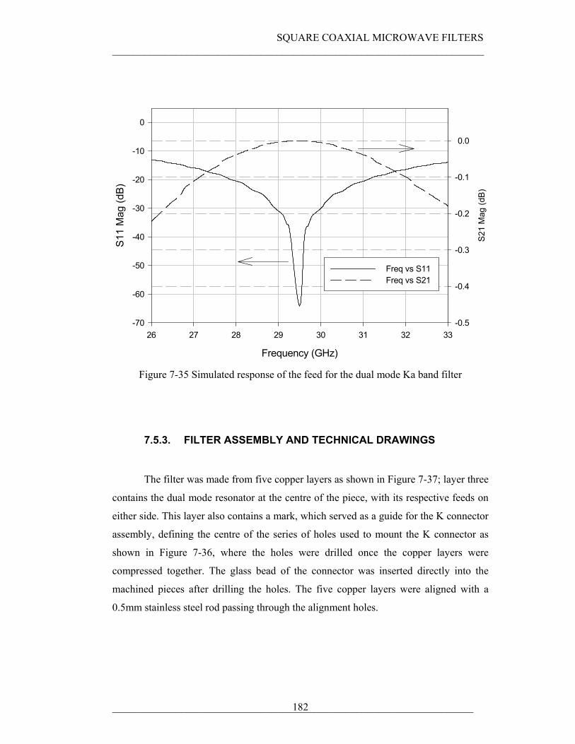
SQUARE COAXIAL MICROWAVE FILTERS ______________________________________________________________________
____________________________________________________________________ 182
Frequency (GHz)
26 27 28 29 30 31 32 33
S11
Mag
(dB)
-70
-60
-50
-40
-30
-20
-10
0
S21
Mag
(dB
)
-0.5
-0.4
-0.3
-0.2
-0.1
0.0
Freq vs S11 Freq vs S21
Figure 7-35 Simulated response of the feed for the dual mode Ka band filter
7.5.3. FILTER ASSEMBLY AND TECHNICAL DRAWINGS
The filter was made from five copper layers as shown in Figure 7-37; layer three
contains the dual mode resonator at the centre of the piece, with its respective feeds on
either side. This layer also contains a mark, which served as a guide for the K connector
assembly, defining the centre of the series of holes used to mount the K connector as
shown in Figure 7-36, where the holes were drilled once the copper layers were
compressed together. The glass bead of the connector was inserted directly into the
machined pieces after drilling the holes. The five copper layers were aligned with a
0.5mm stainless steel rod passing through the alignment holes.
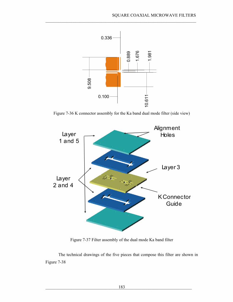
SQUARE COAXIAL MICROWAVE FILTERS ______________________________________________________________________
____________________________________________________________________ 183
1.98
1
1.67
6
0.88
9
10.6
11
9.50
8
0.336
0.100
Figure 7-36 K connector assembly for the Ka band dual mode filter (side view)
K Connector Guide
Alignment Holes
Layer 3
Layer1 and 5
Layer2 and 4
Figure 7-37 Filter assembly of the dual mode Ka band filter
The technical drawings of the five pieces that compose this filter are shown in
Figure 7-38
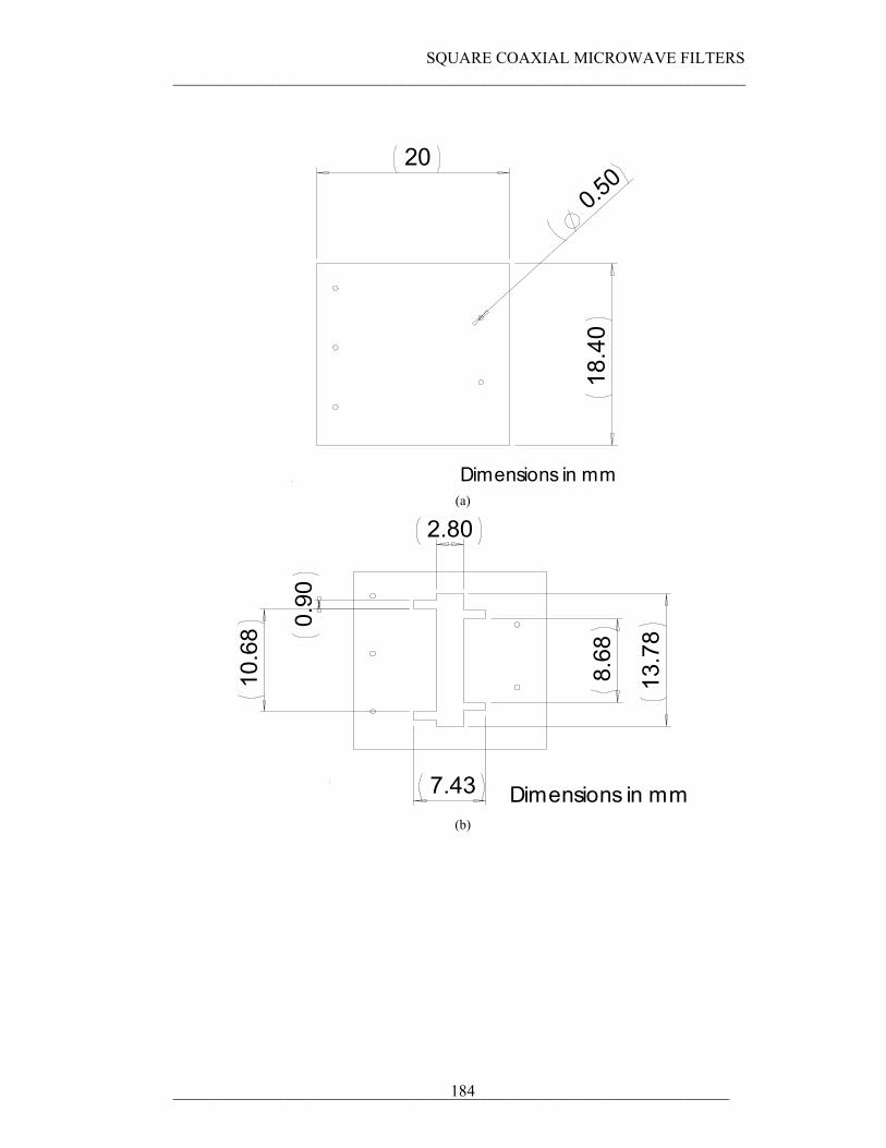
SQUARE COAXIAL MICROWAVE FILTERS ______________________________________________________________________
____________________________________________________________________ 184
20
18.4
0
0.50
Dimensions in mm (a)
8.68
13.7
8
0.90
10.6
8
2.80
7.43 Dimensions in mm (b)
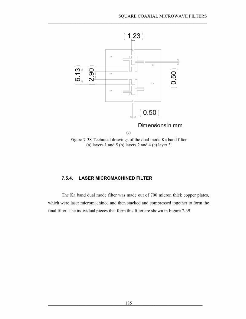
SQUARE COAXIAL MICROWAVE FILTERS ______________________________________________________________________
____________________________________________________________________ 185
1.23
2.90
6.13
0.50
0.50
Dimensions in mm (c)
Figure 7-38 Technical drawings of the dual mode Ka band filter (a) layers 1 and 5 (b) layers 2 and 4 (c) layer 3
7.5.4. LASER MICROMACHINED FILTER
The Ka band dual mode filter was made out of 700 micron thick copper plates,
which were laser micromachined and then stacked and compressed together to form the
final filter. The individual pieces that form this filter are shown in Figure 7-39.
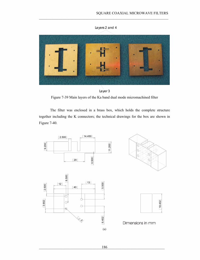
SQUARE COAXIAL MICROWAVE FILTERS ______________________________________________________________________
____________________________________________________________________ 186
Layers 2 and 4
Layer 3
Figure 7-39 Main layers of the Ka band dual mode micromachined filter
The filter was enclosed in a brass box, which holds the complete structure
together including the K connectors; the technical drawings for the box are shown in
Figure 7-40.
5.50
06.
402
2.50
0
8.50
0
4012 13
2
3.90
2
20
11.2
00
0.50
0
2.500
9.20
0
14.450
18.4
02
(a)
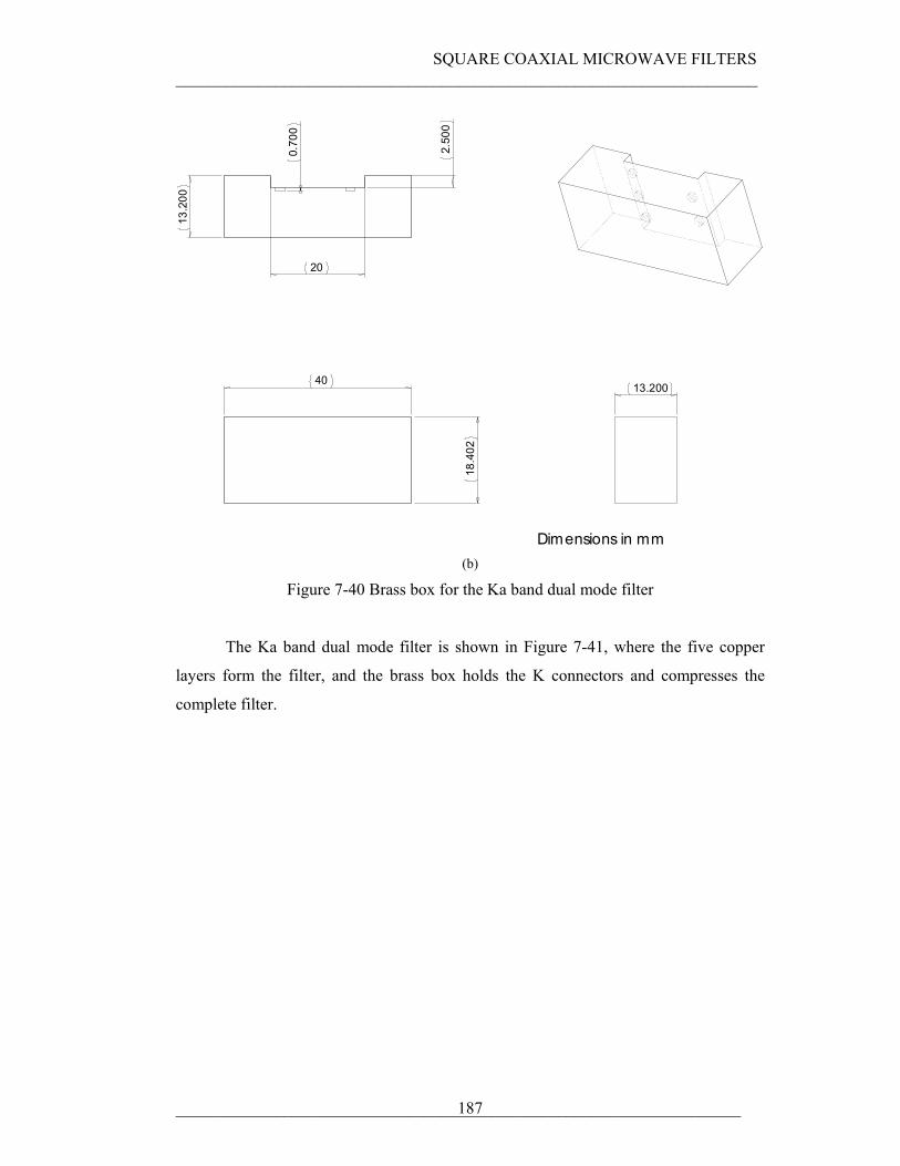
SQUARE COAXIAL MICROWAVE FILTERS ______________________________________________________________________
____________________________________________________________________ 187
Dimensions in mm
40
18.4
02
2.50
0
13.2
00
0.70
0
20
13.200
(b)
Figure 7-40 Brass box for the Ka band dual mode filter
The Ka band dual mode filter is shown in Figure 7-41, where the five copper
layers form the filter, and the brass box holds the K connectors and compresses the
complete filter.
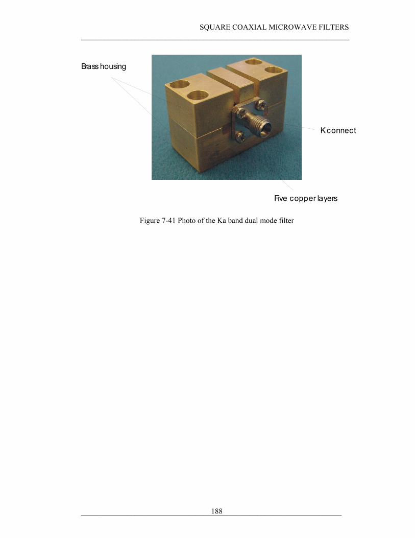
SQUARE COAXIAL MICROWAVE FILTERS ______________________________________________________________________
____________________________________________________________________ 188
Brass housing
Five copper layers
K connect
Figure 7-41 Photo of the Ka band dual mode filter
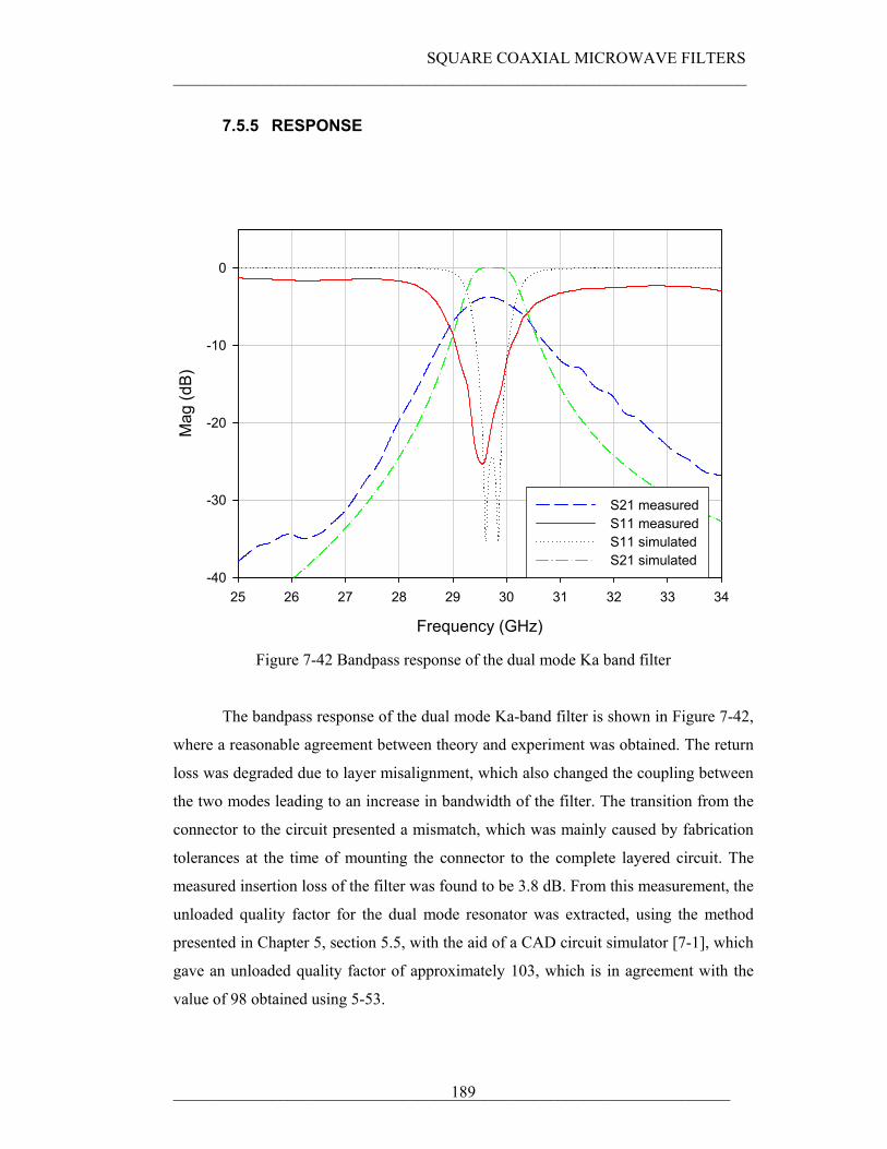
SQUARE COAXIAL MICROWAVE FILTERS ______________________________________________________________________
____________________________________________________________________ 189
7.5.5 RESPONSE
Frequency (GHz)
25 26 27 28 29 30 31 32 33 34
Mag
(dB
)
-40
-30
-20
-10
0
S21 measuredS11 measuredS11 simulatedS21 simulated
Figure 7-42 Bandpass response of the dual mode Ka band filter
The bandpass response of the dual mode Ka-band filter is shown in Figure 7-42,
where a reasonable agreement between theory and experiment was obtained. The return
loss was degraded due to layer misalignment, which also changed the coupling between
the two modes leading to an increase in bandwidth of the filter. The transition from the
connector to the circuit presented a mismatch, which was mainly caused by fabrication
tolerances at the time of mounting the connector to the complete layered circuit. The
measured insertion loss of the filter was found to be 3.8 dB. From this measurement, the
unloaded quality factor for the dual mode resonator was extracted, using the method
presented in Chapter 5, section 5.5, with the aid of a CAD circuit simulator [7-1], which
gave an unloaded quality factor of approximately 103, which is in agreement with the
value of 98 obtained using 5-53.
SQUARE COAXIAL MICROWAVE FILTERS ______________________________________________________________________
____________________________________________________________________ 190
The simulated loss for this Ka-band filter using [4-10] gave an estimated pass
band insertion loss of approximately –0.5 dB, giving a simulated unloaded quality
factor of 750, while the X-band dual mode filter presented in section 7.4 presented a
simulated insertion loss of -0.3 dB giving a simulated unloaded quality factor of 1200.
The increase in the losses in the measured response are believed to be caused by the
surface roughness of the copper plates, combined with the trace of the laser cut, which
may have changed the conductivity of the copper in the case of the Ka-band filter, and
any imperfection in the copper used. These passband simulations do not include
connectors and the transitions from these to the circuit, which also contribute to overall
measured losses.
7.6. CONCLUSIONS
Dielectric supported coaxial filters were presented at the beginning of this
chapter. These presented two challenges, the difficulty to manufacture them, and, as the
design frequency gets higher, finding a good dielectric material to support the centre
conductor of the coaxial structure became an important issue. Then, the idea of making
self-supported coaxial structures was developed and executed with three self-supported
square coaxial filters, which presents an interesting and new way of making low loss
transmission line structures, which consist only of metal, providing low losses which
have the potential for the development of millimetre wave devices.
7.7. REFERENCES
[4-10] HFSS
[7-1] Applied wave research, Microwave office 2001 V 4.0
I.Llamas-Garro, PhD thesis (2003), The University of Birmingham, UK
8. CHAPTER EIGHT
CONCLUSIONS AND FURTHER WORK
8.1. CONCLUSIONS
The first main objective of this research was to find a low loss transmission line for
application in the millimetre wave region. The attempt to do this began with the analysis
of the transmission lines and resonators shown in Chapter 6, in which we concluded that
the square coaxial transmission line was a compact low loss transmission line suitable to
achieve our first main objective.
The second main objective of this research was to find a way of supporting the
centre conductor of the square coaxial structure. At low frequencies, the idea of using
PTFE to support the centre conductor provided the desired low loss. As frequency got
higher, new challenges were presented. The need to find a way of manufacturing a
dielectric supported structure like the ones used in the lower frequency range present the
problem on which material to use, and the method needed to manufacture the whole
CONCLUSIONS AND FURTHER WORK ______________________________________________________________________
____________________________________________________________________ 192
structure. To overcome these challenges, a self-supported layered metal structure was
proposed which consists of suspended metal structures having no dielectric, which
meets the low loss target necessary at the millimetre wave region.
The third main objective of this research was to develop a way to ensemble a square
coaxial transmission line, and the solution found was to stack layers of material which
can be coated in metal. For the Ka band dual mode filter, the structure was directly
machined in copper layers. In this method, layer alignment can be critical, depending on
the overall shape of the microwave circuit.
Despite the fact that the round coaxial transmission line presents better loss
characteristics than the square coaxial transmission line, as shown in Figure 6-9 and
Figure 6-7. The square coaxial was chosen because it presented the possibility to
ensemble the coaxial structure in layers, which allows forming rigid microwave passive
devices.
8.2. FURTHER WORK
The parallel plate waveguide and the deep coplanar waveguide presented in Chapter
6 can be refined, considering that they were the first experiments in this thesis, and
considering that at the time they were designed, we changed structures, which led to the
square coaxial transmission line without giving them more attention. They present
possible construction in the millimetre wave region by using LIGA or SU8
micromachining techniques, since these techniques provide the possibility to produce
high aspect ratio structures.
In the following paragraphs, proposed further work on the square coaxial all metal
structure will be presented. The Ka band, dual mode filter can be fabricated using
different micromachining techniques. The technique used for the filter presented in
Chapter 7 section 7.5.4 will be addressed here. This filter was fabricated using a 45
Watt copper vapour laser at Oxford Lasers Ltd., with a repetition rate of 10 to 12 KHz,
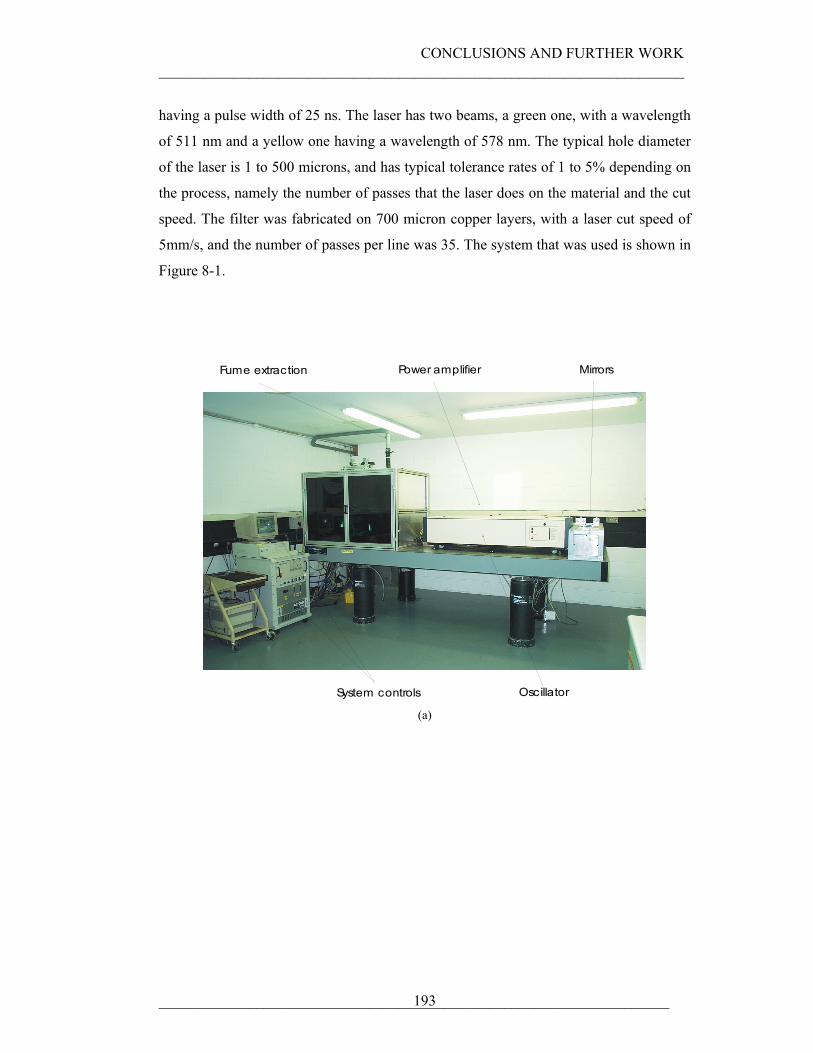
CONCLUSIONS AND FURTHER WORK ______________________________________________________________________
____________________________________________________________________ 193
having a pulse width of 25 ns. The laser has two beams, a green one, with a wavelength
of 511 nm and a yellow one having a wavelength of 578 nm. The typical hole diameter
of the laser is 1 to 500 microns, and has typical tolerance rates of 1 to 5% depending on
the process, namely the number of passes that the laser does on the material and the cut
speed. The filter was fabricated on 700 micron copper layers, with a laser cut speed of
5mm/s, and the number of passes per line was 35. The system that was used is shown in
Figure 8-1.
Fume extraction Power amplifier
Oscillator
Mirrors
System controls (a)
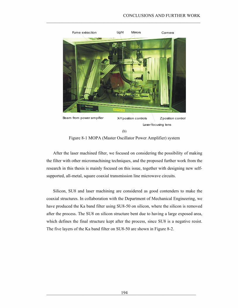
CONCLUSIONS AND FURTHER WORK ______________________________________________________________________
____________________________________________________________________ 194
Camera
Laser focusing lens
Fume extraction
Beam from power ampifier X-Y position controls Z position control
MirrorsLight
(b)
Figure 8-1 MOPA (Master Oscillator Power Amplifier) system
After the laser machined filter, we focused on considering the possibility of making
the filter with other micromachining techniques, and the proposed further work from the
research in this thesis is mainly focused on this issue, together with designing new self-
supported, all-metal, square coaxial transmission line microwave circuits.
Silicon, SU8 and laser machining are considered as good contenders to make the
coaxial structures. In collaboration with the Department of Mechanical Engineering, we
have produced the Ka band filter using SU8-50 on silicon, where the silicon is removed
after the process. The SU8 on silicon structure bent due to having a large exposed area,
which defines the final structure kept after the process, since SU8 is a negative resist.
The five layers of the Ka band filter on SU8-50 are shown in Figure 8-2.
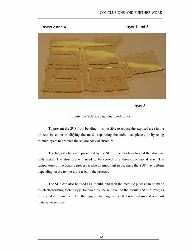
CONCLUSIONS AND FURTHER WORK ______________________________________________________________________
____________________________________________________________________ 195
Layer 1 and 5Layers 2 and 4
Layer 3
Figure 8-2 SU8 Ka band dual mode filter
To prevent the SU8 from bending, it is possible to reduce the exposed area in the
process by either modifying the mask, separating the individual pieces, or by using
thinner layers to produce the square coaxial structure.
The biggest challenge presented by the SU8 filter was how to coat the structure
with metal. The structure will need to be coated in a three-dimensional way. The
temperature of the coating process is also an important issue, since the SU8 may deform
depending on the temperature used in the process.
The SU8 can also be used as a mould, and then the metallic pieces can be made
by electroforming technology, followed by the removal of the mould and substrate, as
illustrated in Figure 8-3. Here the biggest challenge is the SU8 removal since it is a hard
material to remove.
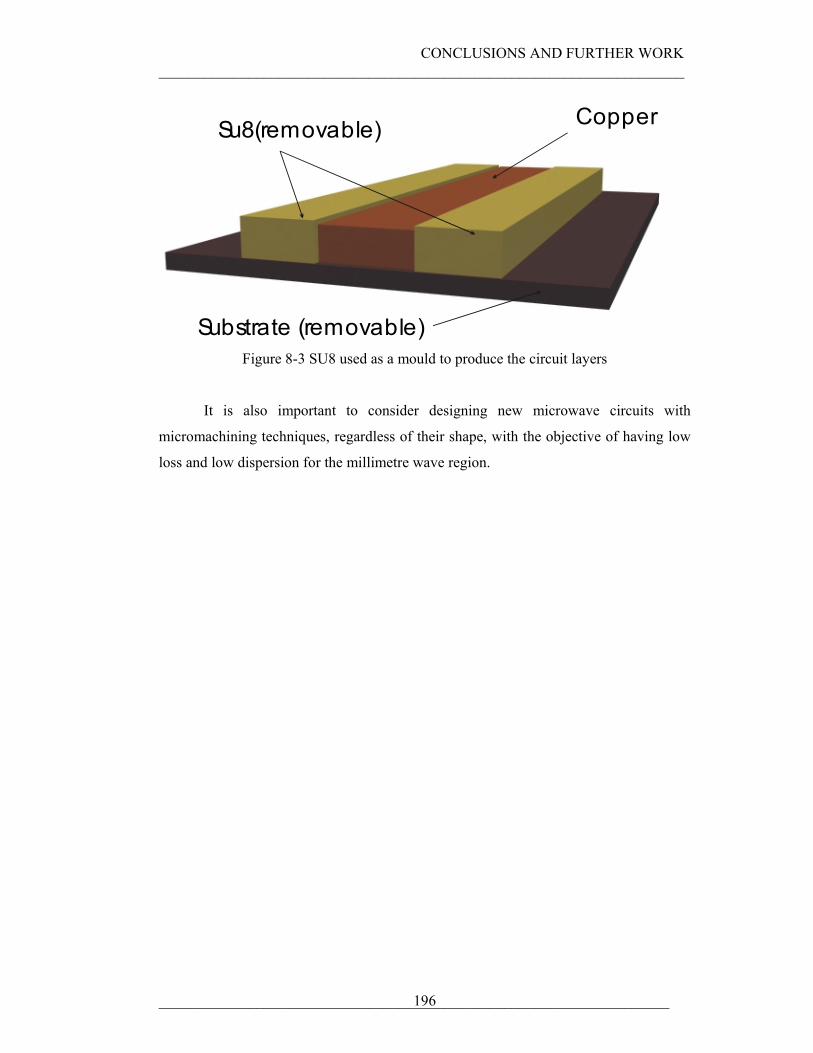
CONCLUSIONS AND FURTHER WORK ______________________________________________________________________
____________________________________________________________________ 196
Su8(removable) Copper
Substrate (removable) Figure 8-3 SU8 used as a mould to produce the circuit layers
It is also important to consider designing new microwave circuits with
micromachining techniques, regardless of their shape, with the objective of having low
loss and low dispersion for the millimetre wave region.
I.Llamas-Garro, PhD thesis (2003), The University of Birmingham, UK
197
1. APENDIX
PUBLICATION LIST
Journal papers
• K. Jiang, M.J Lancaster, I. Llamas-Garro and P. Jin, “SU-8 Ka-band filter and its microfabrication”, Journal of Micromechanics and Microengineering, Vol 15, No. 8, August 2005, pp 1522-1526.
• I.Llamas-Garro, M.J.Lancaster, and P.S.Hall, “Air filled square coaxial transmission line and its use in microwave filters”, IEE proc. on microwaves antennas and propagation, Vol. 152, No. 3, June 2005, pp. 155-159.
• I.Llamas-Garro, M.J.Lancaster, and P.S.Hall, “Erratum to: A low loss wideband suspended coaxial transmission line”, Microwave and optical technology letters, Vol. 43, No. 6, 2004, pp 543.
• I.Llamas-Garro, M.J.Lancaster, and P.S.Hall, “A low loss wideband suspended coaxial transmission line”, Microwave and optical technology letters, Vol. 43, No. 2, 2004, pp 93-95.
Conference papers
• I.Llamas-Garro, K.Jiang, P.Jin, and M.J.Lancaster, “SU-8 Microfabrication for a Ka-Band filter” MEMSWAVE, 4th Workshop on MEMS for millimeter wave communications, LAAS-CNRS, Toulouse, France, 2nd – 4th of July 2003. pp F55-F58.
• I.Llamas-Garro, M.J.Lancaster, and P.S.Hall, “A high Q, X-band square coaxial resonator and filter design”, EPSRC PREP 2002 conference, University of Nottingham, United Kingdom, 17th-19th April 2002, pp 1-2.