Embed Size (px)
Citation preview
Micromax30 Watt Solid-State
FM Exciter
Operation Manual

WARNING: Disconnect primary power prior to servicing
Harris Micromax FM Exciter REV 2 01/7/2008

Harris Micromax FM Exciter REV 2 01/7/2008
WARNING: Disconnect primary power prior to servicing
1. Preliminary Instructions
This manual is written as a general guide for those having previous knowledge and experience
with this kind of equipment.
It is not intended to contain a complete statement of all safety rules which should be observed by
personnel in using this or other electronic equipment.
The installation, use and maintenance of this piece of equipment involve risks both for the personnel
performing them and for the device itself, that shall be used only by trained personnel.
Harris does not assume responsibility for injury or damage resulting from improper procedures
or practices by untrained/unqualified personnel in the handling of this unit.
Please observe all local codes and fire protection standards in the operation of this unit.
WARNING: Always disconnect power before opening covers or removing any part of this unit.
Use appropriate grounding procedures to short out capacitors and high voltage points before
servicing.
Harris Corporation reserves the right to modify the design and/or the technical specifications of
the product and this manual without notice.
WARNING: Disconnect primary power prior to servicing
Harris Micromax FM Exciter REV 2 01/7/2008
2. First Aid
The personnel employed in the installation, use and maintenance of the device, shall be familiar
with theory and practice of first aid..
2.1 Treatment of electrical shocks
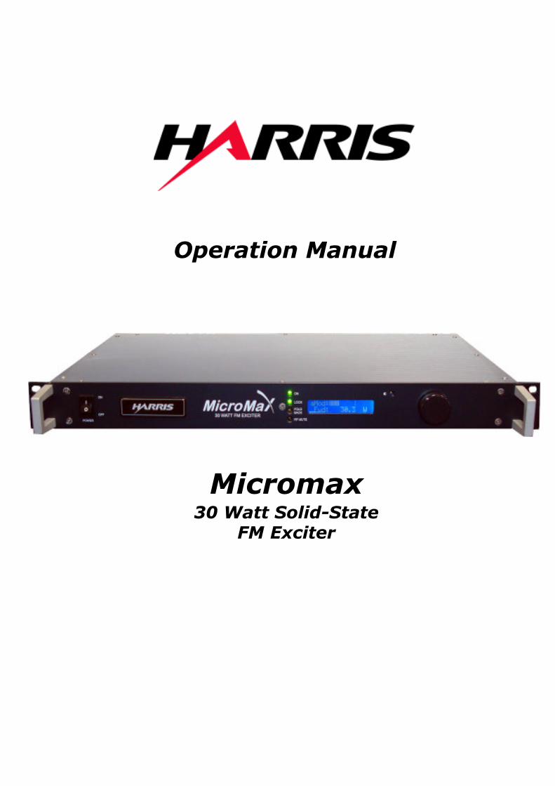
2.1.1 If the victim is not responsive
Follow the A-B-C's of basic life support
• Place victim flat on his back on a hard surface.
• Open airway: lift up neck, push forehead back (Fig. 3-1).
• Clear out mouth if necessary and observe for breathing
• If not breathing, begin artificial breathing (Figure 3-2): tilt head, pinch nostrils, make airtight
seal, four quick full breaths. Remember mouth to mouth resuscitation must be commenced as
soon as possible
Figure 3-1 Figure 3-2
• Check for pulse (Fig 3-3); if pulse is absent, begin artificial circulation
(Fig. 3-4) depressing sternum (Fig. 3-5)
Figure 3-3 Figure 3-4 Figure 3-5
• In case of only one rescuer, 15 compressions alternated to two breaths.
• If there are two rescuers, the rhythm shall be of one breath each 5 compressions.
• Do not interrupt the rhythm of compressions when the second person is giving breath.
• Call for medical assistance as soon as possible.
Harris Micromax FM Exciter REV 2 01/7/2008
WARNING: Disconnect primary power prior to servicing
2.1.2 If victim is responsive
• Keep them warm
• Keep them as quiet as possible
• Loosen their clothing (a reclining position is recommended)
• Call for medical help as soon as possible
2.2 Treatment of electrical Burns
2.2.1 Extensive burned and broken skin
• Cover area with clean sheet or cloth
• Do not break blisters, remove tissue, remove adhered particles of clothing, or apply any
salve or ointment.
• Treat victim for shock as required.
• Arrange transportation to a hospital as quickly as possible.
• If arms or legs are affected keep them elevated
If medical help will not be available within an hour and the victim is conscious and not vomiting,
give him a weak solution of salt and soda: 1 level teaspoonful of salt and 1/2 level teaspoonful of
baking soda to each quart of water (neither hot or cold). Allow victim to sip slowly about 4
ounces (half a glass) over a period of 15 minutes. Discontinue fluid if vomiting occurs
DO NOT give alcohol
2.2.2 Less severe burns
• Apply cool (not ice cold) compresses using the cleansed available cloth article.
• Do not break blisters, remove tissue, remove adhered particles of clothing, or apply salve or
ointment.
• Apply clean dry dressing if necessary.
• Treat victim for shock as required.
• Arrange transportation to a hospital as quickly as possible
• If arms or legs are affected keep them elevated.

WARNING: Disconnect primary power prior to servicing
Harris Micromax FM Exciter REV 2 01/7/2008
Harris Micromax FM Exciter REV 2 01/7/2008
WARNING: Disconnect primary power prior to servicing
TABLE OF CONTENTSPage
SECTION 1 General Description
1.1 Introduction 1-1
1.2 Equipment function 1-1
1.3 Physical description 1-1
1.4 Electrical description 1-2
1.5 Simplified block diagrams 1-2
1.6 List of subsystems 1-2
SECTION 2 Installation
2.1 Introduction 2-1
2.2 Unpacking 2-1
2.3 Returns and exchanges 2-1
2.4 Installation 2-1
2.4.1 A/C power connection 2-1
2.4.2 RF output connection 2-2
2.4.3 Audio input connections 2-2
2.4.3.1 MPX (composite) audio input connection 2-3
2.4.3.2 Mono audio input connection 2-3
2.4.3.3 Left and right channel audio inputs 2-4
2.4.3.4 AES/EBU audio inputs 2-4
2.4.4 Remote I/O connector 2-5
2.4.5 Service connector 2-6
SECTION 3 Operation
3.1 Introduction 3-1
3.2 Turning on the exciter 3-1
3.3 Adjusting RF power output 3-2
3.4 Operating frequency selection 3-3
3.5 Adjusting modulation deviation level 3-4
3.6 Front panel LCD display menu description 3-5
3.6.1 Operations menu 3-5
3.6.2 Power menu 3-6
3.6.3 Power amplifier menu 3-6
3.6.4 Settings menu 3-6
3.6.5 Miscellaneous menu 3-6
3.6.6 Versions menu 3-6
3.6.7 Channels menu 3-6
Harris Micromax FM Exciter System Overview REV2 01/7/2008
1-1 WARNING: Disconnect primary power prior to servicing
SECTION 1System Overview
1.1 Introduction
This section contains system overview information and covers the following topics:
• Equipment Function (1.2)• Physical Description (1.3)• System Front and Rear Views (1.4)• Simplified Block Diagrams (1.5)• List of Subsystems (1.6)• Technical and Mechanical Specifications (Tables 1.1)
1.2 Equipment function
The Harris Micromax is a 30 Watt FM exciter designed to operate in the 88-108 MHz range in 10kHz steps. The RF power is adjustable continuously from 0-100% of rated power. It is designed to handleMPX (composite), mono and left/right audio inputs with the built-in stereo generator. The internal stereogenerator can be turned on or off in the field.
In addition, an optional AES/EBU module is available for digital audio input capability.
In keeping with the design philosophy of modularity and maintainability, Micromax uses easily removableand serviceable subsystems. List of subsystems is outlined in section 1.6.
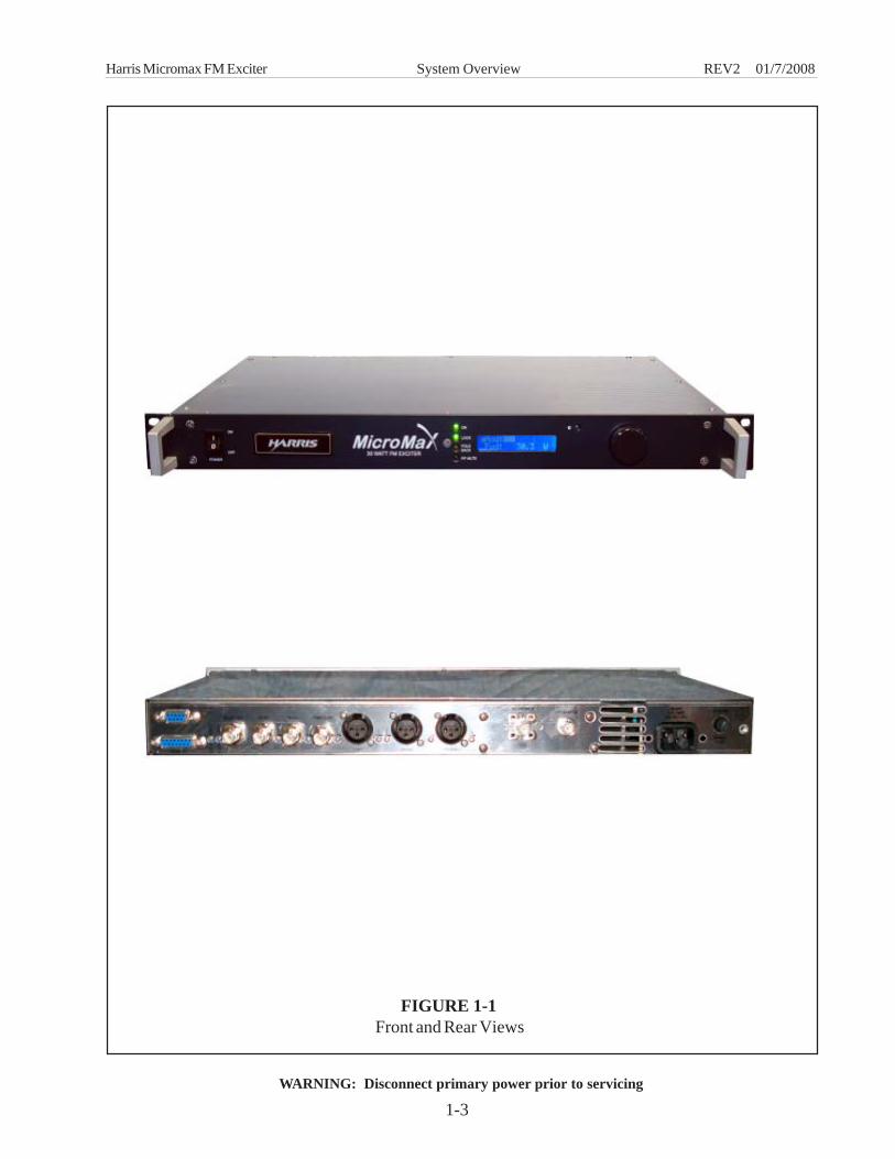
1.3 Physical description
Micromax is electrically and mechanically modular in design. The entire system is contained in a 19”rack that is 1.75” high. All subsystems are assembled with removable connectors to allow for easy servicingand replacement.
The front panel contains an LCD display for metering and control, a menu navigation and selectionknob, on/off switch and status LEDs.
Rear panel contains AC input block, RF connectors, audio connectors, remote control and monitoringconnectors.
See Figure 1-1 for front and rear views of the Micromax FM exciter.
1-2 WARNING: Disconnect primary power prior to servicing
Harris Micromax FM Exciter System Overview REV2 01/7/2008
1.4 Electrical description
Micromax is a self contained broadband FM exciter. The frequency of operation and RF power levelare selectable from the front panel. A microprocessor controller monitors all operating parameters andautomatically lowers RF output in case of high VSWR or temperature.
Unit is powered by a high efficiency, universal AC input (80-260VAC) switching power supply. TheRF output module is totally broadband across the FM band and is capable of delivering RF output power ofup to 30 Watts.
Technical specifications of the Micromax is shown in Table 1-1.
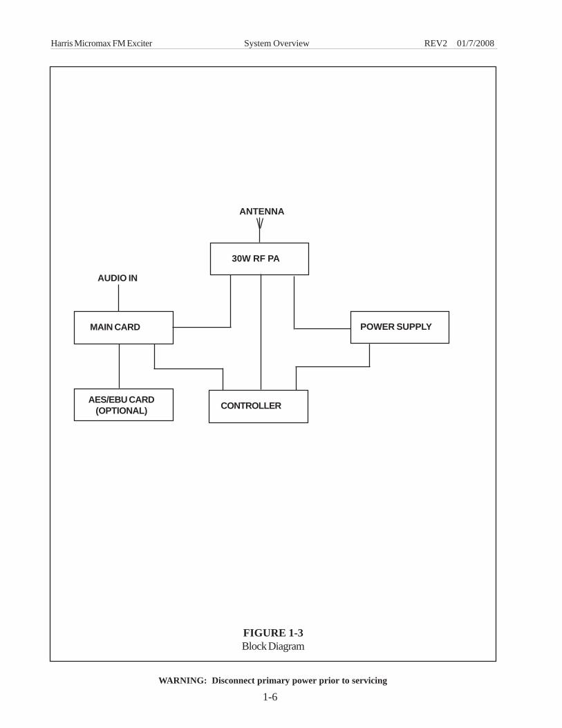
1.5 Simplified block diagrams
Micromax is composed of modular subsystems that are easily removable and serviceable.
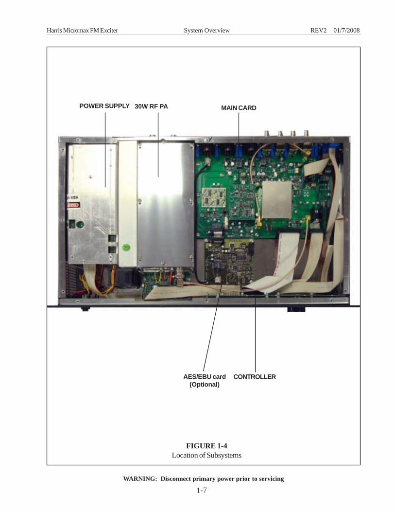
A simplified block diagram of how all the subsystems are interconnected is shown in Figure 1-3.Location of subsystems is shown in Figure 1-4.
1.6 List of subsystems
Micromax is composed of the following subsystems:
1. Power supply2. Main card3. Controller card4. RF Power amplifier
5. AES/EBU card (optional)
Harris Micromax FM Exciter System Overview REV2 01/7/2008
1-3 WARNING: Disconnect primary power prior to servicing
FIGURE 1-1 Front and Rear Views
1-4 WARNING: Disconnect primary power prior to servicing
Harris Micromax FM Exciter System Overview REV2 01/7/2008
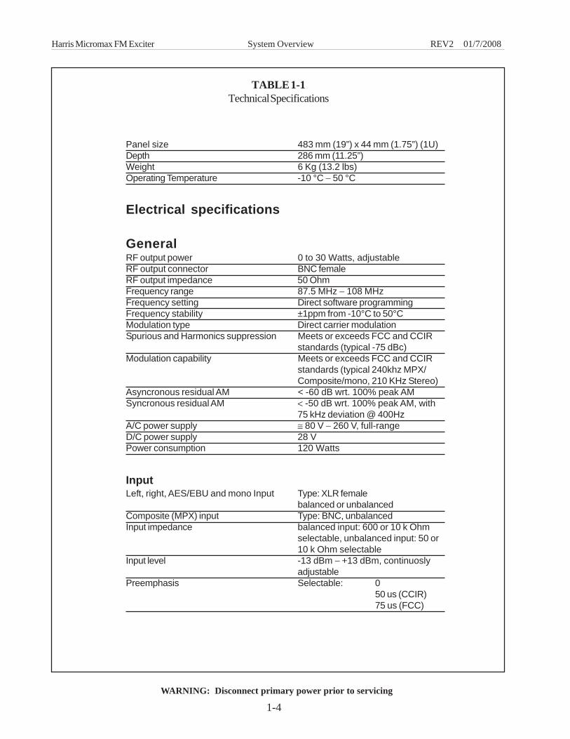
TABLE 1-1Technical Specifications
Panel size 483 mm (19”) x 44 mm (1.75”) (1U)Depth 286 mm (11.25”)Weight 6 Kg (13.2 lbs)Operating Temperature -10 °C − 50 °C
Electrical specifications
GeneralRF output power 0 to 30 Watts, adjustableRF output connector BNC femaleRF output impedance 50 OhmFrequency range 87.5 MHz − 108 MHzFrequency setting Direct software programmingFrequency stability ±1ppm from -10°C to 50°CModulation type Direct carrier modulationSpurious and Harmonics suppression Meets or exceeds FCC and CCIR
standards (typical -75 dBc)Modulation capability Meets or exceeds FCC and CCIR
standards (typical 240khz MPX/Composite/mono, 210 KHz Stereo)
Asyncronous residual AM < -60 dB wrt. 100% peak AMSyncronous residual AM < -50 dB wrt. 100% peak AM, with
75 kHz deviation @ 400HzA/C power supply ≅ 80 V − 260 V, full-rangeD/C power supply 28 VPower consumption 120 Watts
InputLeft, right, AES/EBU and mono Input Type: XLR female
balanced or unbalancedComposite (MPX) input Type: BNC, unbalancedInput impedance balanced input: 600 or 10 k Ohm
selectable, unbalanced input: 50 or10 k Ohm selectable
Input level -13 dBm − +13 dBm, continuoslyadjustable
Preemphasis Selectable: 050 us (CCIR)75 us (FCC)
Harris Micromax FM Exciter System Overview REV2 01/7/2008
1-5 WARNING: Disconnect primary power prior to servicing
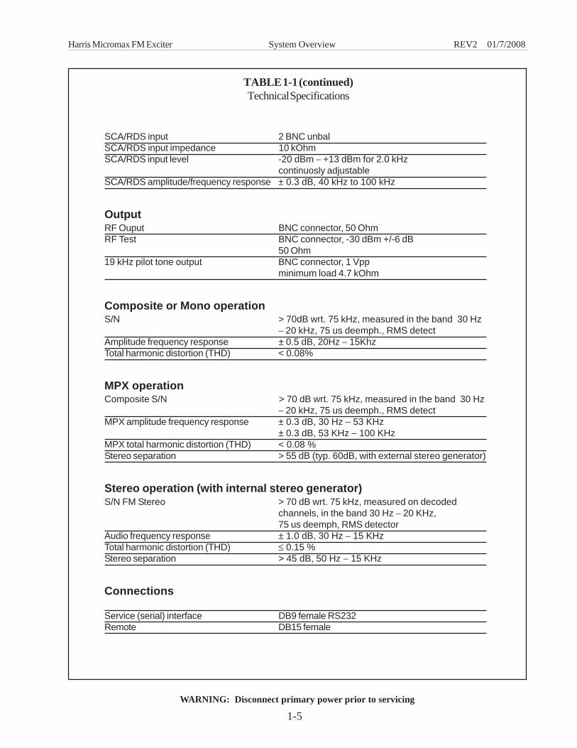
SCA/RDS input 2 BNC unbalSCA/RDS input impedance 10 kOhmSCA/RDS input level -20 dBm − +13 dBm for 2.0 kHz
continuosly adjustableSCA/RDS amplitude/frequency response ± 0.3 dB, 40 kHz to 100 kHz
OutputRF Ouput BNC connector, 50 OhmRF Test BNC connector, -30 dBm +/-6 dB
50 Ohm19 kHz pilot tone output BNC connector, 1 Vpp
minimum load 4.7 kOhm
Composite or Mono operationS/N > 70dB wrt. 75 kHz, measured in the band 30 Hz
− 20 kHz, 75 us deemph., RMS detectAmplitude frequency response ± 0.5 dB, 20Hz − 15KhzTotal harmonic distortion (THD) < 0.08%
MPX operationComposite S/N > 70 dB wrt. 75 kHz, measured in the band 30 Hz
− 20 kHz, 75 us deemph., RMS detectMPX amplitude frequency response ± 0.3 dB, 30 Hz − 53 KHz
± 0.3 dB, 53 KHz − 100 KHzMPX total harmonic distortion (THD) < 0.08 %Stereo separation > 55 dB (typ. 60dB, with external stereo generator)
Stereo operation (with internal stereo generator)S/N FM Stereo > 70 dB wrt. 75 kHz, measured on decoded
channels, in the band 30 Hz − 20 KHz,75 us deemph, RMS detector
Audio frequency response ± 1.0 dB, 30 Hz − 15 KHzTotal harmonic distortion (THD) ≤ 0.15 %Stereo separation > 45 dB, 50 Hz − 15 KHz
Connections
Service (serial) interface DB9 female RS232Remote DB15 female
TABLE 1-1 (continued)Technical Specifications
1-6 WARNING: Disconnect primary power prior to servicing
Harris Micromax FM Exciter System Overview REV2 01/7/2008
FIGURE 1-3Block Diagram
ANTENNA
MAIN CARD
CONTROLLERAES/EBU CARD(OPTIONAL)
30W RF PA
POWER SUPPLY
AUDIO IN
Harris Micromax FM Exciter System Overview REV2 01/7/2008
1-7 WARNING: Disconnect primary power prior to servicing
MAIN CARD
CONTROLLER
30W RF PAPOWER SUPPLY
FIGURE 1-4Location of Subsystems
AES/EBU card(Optional)
Harris Micromax FM Exciter Installation REV2 01/7/2008
2-1
WARNING: Disconnect primary power prior to servicing
SECTION 2
Installation
2.1 Introduction
This section contains information on how to install the exciter and covers the following topics:
• Unpacking (2.2)
• Returns and Exchanges (2.3)
• Installation (2.4)
• A/C power connection (2.4.1)
• RF output connection (2.4.2)
• Audio input connections (2.4.3)
• Remote I/O connector (2.4.5)
• Service connector (2.4.5)
2.2 Unpacking
The unit is shipped in a cardboard box. The shipping box also contains the manual and the A/C power
cord. Open the box and perform a visual check to determine that there was no physical damage during
shipment. Note any damage on the bill of lading and retain shipping documents.
If the contents are incomplete or if the unit is damaged, contact the carrier and factory immediately.
Time limit to file damage claims with the carrier is 14 days.
2.3 Returns and exchanges
Damaged or undamaged equipment should not be returned without first obtaining return authorization
from factory. Factory will provide special shipping instructions and provide a RMA number to insure proper
handling. If you need to return the unit, contact the customer service department at factory and have your
model number and serial number available. Serial number is located on the rear panel.
2.4 Installation
Prior to installation, the manual should be carefully studied to get an overall understanding of the
system. This will facilitate proper installation and initial checkout.
2-2
WARNING: Disconnect primary power prior to servicing
Harris Micromax FM Exciter Installation REV2 01/7/2008
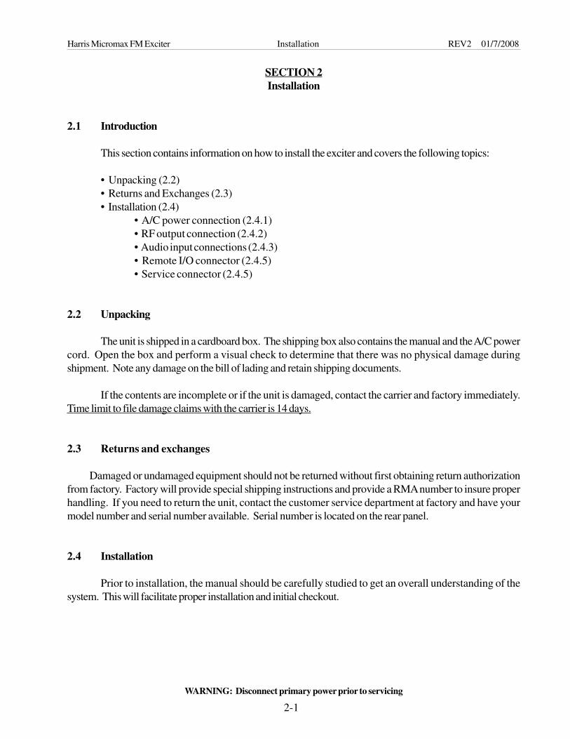
2.4.1 A/C Power connection
The Micromax operates on 80-260 Volts AC (50 or 60 Hz single phase)
Connect the AC power on rear panel.
2.4.2 RF output connection
Connect an antenna or an RF load to the type BNC female RF output connector on the rear panel.
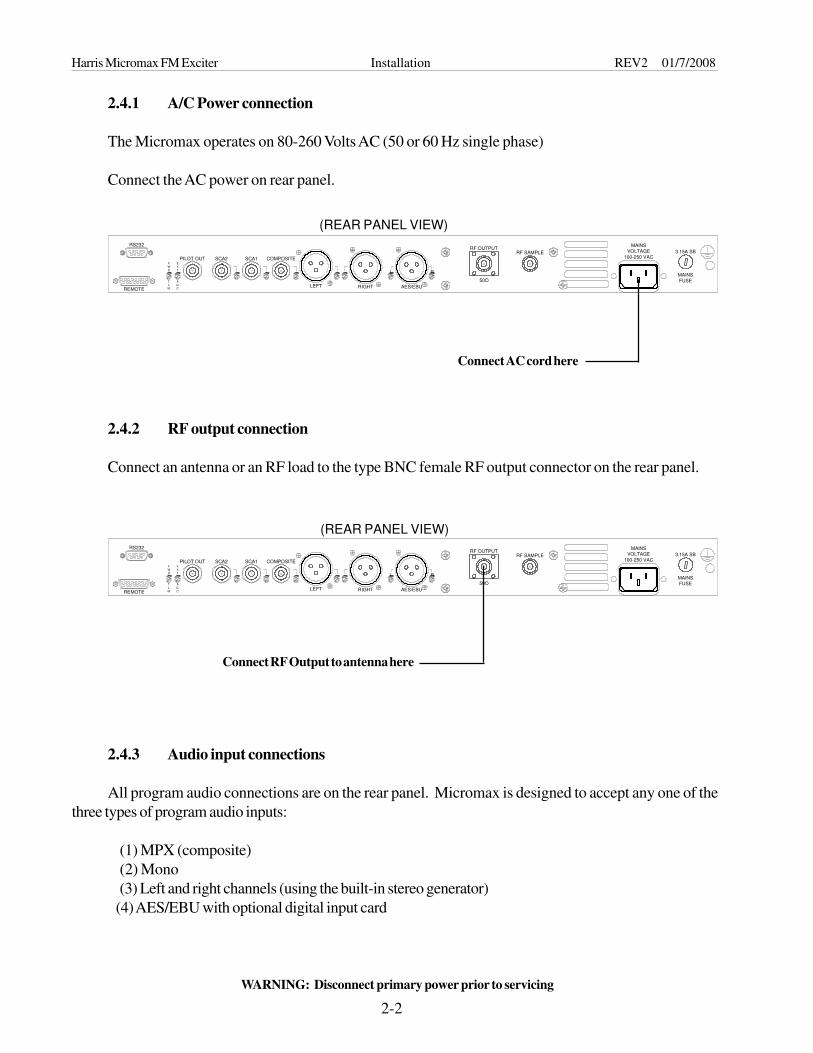
2.4.3 Audio input connections
All program audio connections are on the rear panel. Micromax is designed to accept any one of the
three types of program audio inputs:
(1) MPX (composite)
(2) Mono
(3) Left and right channels (using the built-in stereo generator)
(4) AES/EBU with optional digital input card
PILOT OUT SCA2 SCA1 COMPOSITEF
W
D
T
LM
E
X
T
A
GC
RS232
REMOTELEFT RIGHT AES/EBU
50O
RF OUTPUTRF SAMPLE
MAINS VOLTAGE
100-250 VAC3.15A SB
MAINS FUSE
L R
PILOT OUT SCA2 SCA1 COMPOSITEF
W
D
T
LM
E
X
T
A
GC
RS232
REMOTELEFT RIGHT AES/EBU
50O
RF OUTPUTRF SAMPLE
MAINS VOLTAGE
100-250 VAC3.15A SB
MAINS FUSE
L R
Connect AC cord here
Connect RF Output to antenna here
(REAR PANEL VIEW)
(REAR PANEL VIEW)
Harris Micromax FM Exciter Installation REV2 01/7/2008
2-3
WARNING: Disconnect primary power prior to servicing
PILOT OUT SCA2 SCA1 COMPOSITEF
W
D
T
LM
E
X
T
A
GC
RS232
REMOTELEFT RIGHT AES/EBU
50O
RF OUTPUTRF SAMPLE
MAINS VOLTAGE
100-250 VAC3.15A SB
MAINS FUSE
L R
PILOT OUT SCA2 SCA1 COMPOSITEF
WD
T
LM
E
XT
A
GC
RS232
REMOTELEFT RIGHT AES/EBU
50O
RF OUTPUTRF SAMPLE
MAINS VOLTAGE
100-250 VAC3.15A SB
MAINS FUSE
L R
2.4.3.1 MPX (composite) audio input connection
Connect MPX (composite) audio input to BNC connector on rear panel. On the front panel LCD
display, go to SET menu and select mono (composite) from the audio mono/stereo selection (see section 3 of
manual on how to navigate the LCD display).
2.4.3.2 Mono audio input connection
Connect Mono audio input to XLR connector on rear panel. On the front panel LCD display, go to SET
menu and select mono (composite) from the audio mono/stereo selection (see section 3 of manual on how to
navigate the LCD display).
Connect mono audio input here
Connect MPX (composite) audio input here
(REAR PANEL VIEW)
(REAR PANEL VIEW)
2-4
WARNING: Disconnect primary power prior to servicing
Harris Micromax FM Exciter Installation REV2 01/7/2008
PILOT OUT SCA2 SCA1 COMPOSITEF
W
D
T
LM
E
X
T
A
GC
RS232
REMOTELEFT RIGHT AES/EBU
50O
RF OUTPUTRF SAMPLE
MAINS VOLTAGE
100-250 VAC3.15A SB
MAINS FUSE
L R
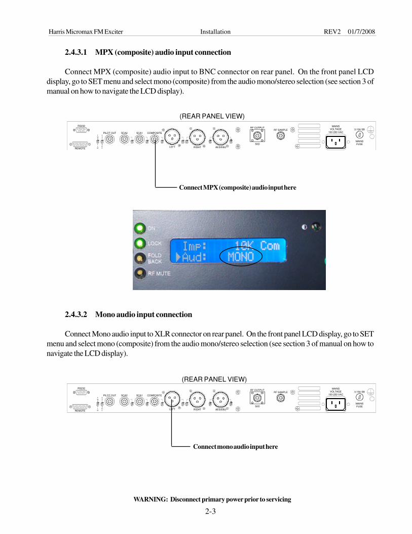
2.4.3.3 Left and right channel audio inputs (using the built-in stereo generator)
Connect left and right channel audio inputs to XLR connectors on rear panel. On the front panel LCD
display, go to SET menu and select stereo from the audio mono/stereo selection (see section 3 of manual on
how to navigate the LCD display). This will activate the built-in stereo generator and turn on the 19 kHz stereo
pilot tone at 10% injection.
Connect left audio input here Connect right audio input here
(REAR PANEL VIEW)
2.4.3.4 AES/EBU Input (using the built-in OPTIONAL AES/EBU card)
Connect AES/EBU input to XLR connector on rear panel. On the front panel LCD display, go to SET
menu and select stereo from the audio mono/stereo selection as shown above (sec 2.4.3.3) (see section 3 of
manual on how to navigate the LCD display). When an audio is applied to AES/EBU input, the main display
will indicate “dMod” (digital modulation) as shown below.
PILOT OUT SCA2 SCA1 COMPOSITEF
WD
T
LM
E
XT
A
GC
RS232
REMOTELEFT RIGHT AES/EBU
50O
RF OUTPUTRF SAMPLE
MAINS VOLTAGE
100-250 VAC3.15A SB
MAINS FUSE
L R
Connect AES/EBU input here
Harris Micromax FM Exciter Installation REV2 01/7/2008
2-5
WARNING: Disconnect primary power prior to servicing
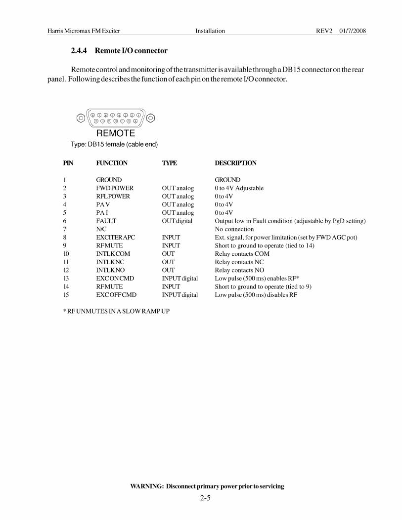
2.4.4 Remote I/O connector
Remote control and monitoring of the transmitter is available through a DB15 connector on the rear
panel. Following describes the function of each pin on the remote I/O connector.
Type: DB15 female (cable end)
PIN FUNCTION TYPE DESCRIPTION
1 GROUND GROUND
2 FWD POWER OUT analog 0 to 4V Adjustable
3 RFL POWER OUT analog 0 to 4V
4 PA V OUT analog 0 to 4V
5 PA I OUT analog 0 to 4V
6 FAULT OUT digital Output low in Fault condition (adjustable by PgD setting)
7 N/C No connection
8 EXCITER APC INPUT Ext. signal, for power limitation (set by FWD AGC pot)
9 RF MUTE INPUT Short to ground to operate (tied to 14)
10 INTLK COM OUT Relay contacts COM
11 INTLK NC OUT Relay contacts NC
12 INTLK NO OUT Relay contacts NO
13 EXC ON CMD INPUT digital Low pulse (500 ms) enables RF*
14 RF MUTE INPUT Short to ground to operate (tied to 9)
15 EXC OFF CMD INPUT digital Low pulse (500 ms) disables RF
* RF UNMUTES IN A SLOW RAMP UP
1
9
2
10
3
11
4
12
5
13
6
14
7
15
8
REMOTE
2-6
WARNING: Disconnect primary power prior to servicing
Harris Micromax FM Exciter Installation REV2 01/7/2008
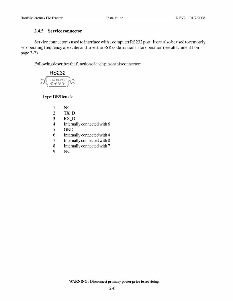
2.4.5 Service connector
Service connector is used to interface with a computer RS232 port. It can also be used to remotely
set operating frequency of exciter and to set the FSK code for translator operation (see attachment 1 on
page 3-7).
Following describes the function of each pin on this connector:
Type: DB9 female
1 NC
2 TX_D
3 RX_D
4 Internally connected with 6
5 GND
6 Internally connected with 4
7 Internally connected with 8
8 Internally connected with 7
9 NC
1
6
2
7
3
8
4
9
5
RS232
Harris Micromax FM Exciter Operation REV2 01/7/2008
3-1
WARNING: Disconnect primary power prior to servicing
SECTION 3
Operation
3.1 Introduction
This section of the manual contains information on how to operate the exciter and covers the following
topics:
• Turning on the transmitter (3.2)
• Adjusting RF power output (3.3)
• Operating frequency selection (3.4)
• Adjusting modulation deviation level (3.5)
• Front panel LCD display menu description (3.6)
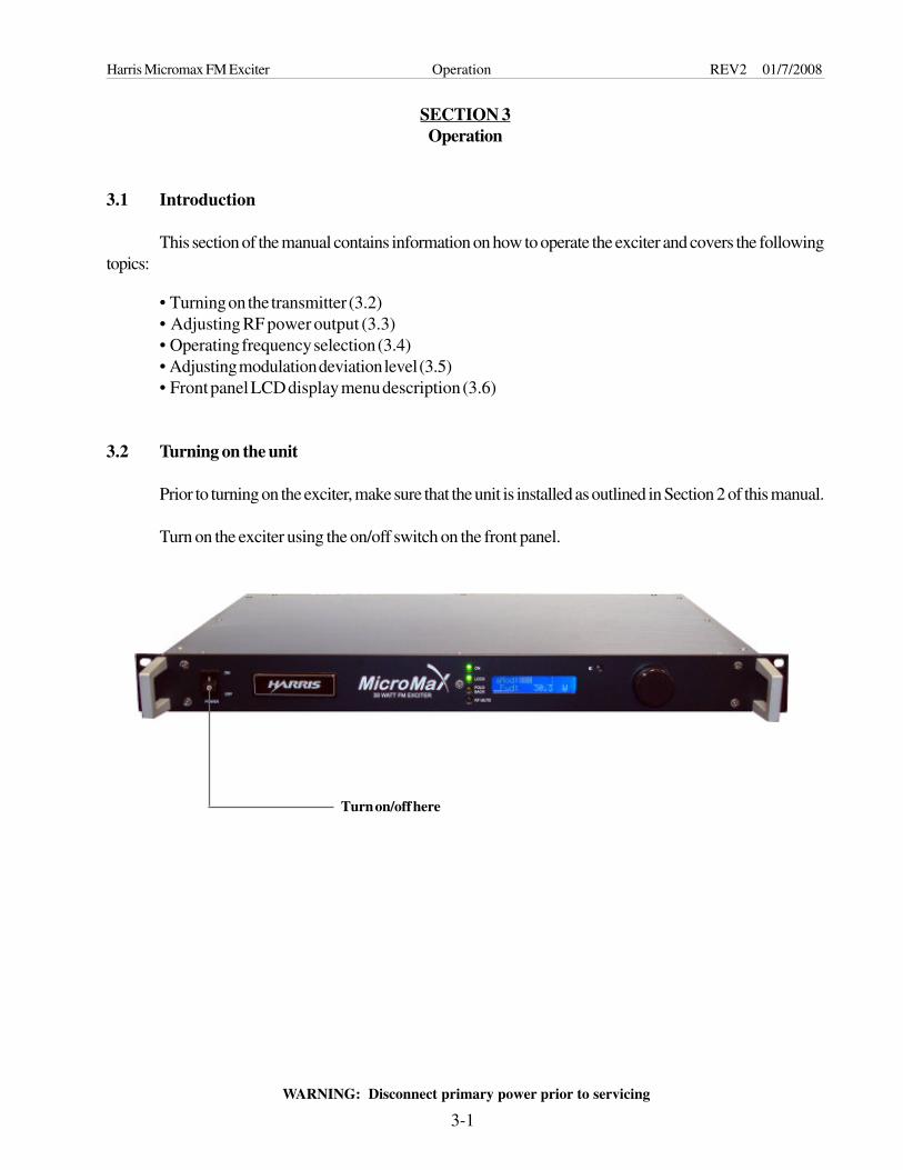
3.2 Turning on the unit
Prior to turning on the exciter, make sure that the unit is installed as outlined in Section 2 of this manual.
Turn on the exciter using the on/off switch on the front panel.
Turn on/off here
3-2
WARNING: Disconnect primary power prior to servicing
Harris Micromax FM Exciter Operation REV2 01/7/2008
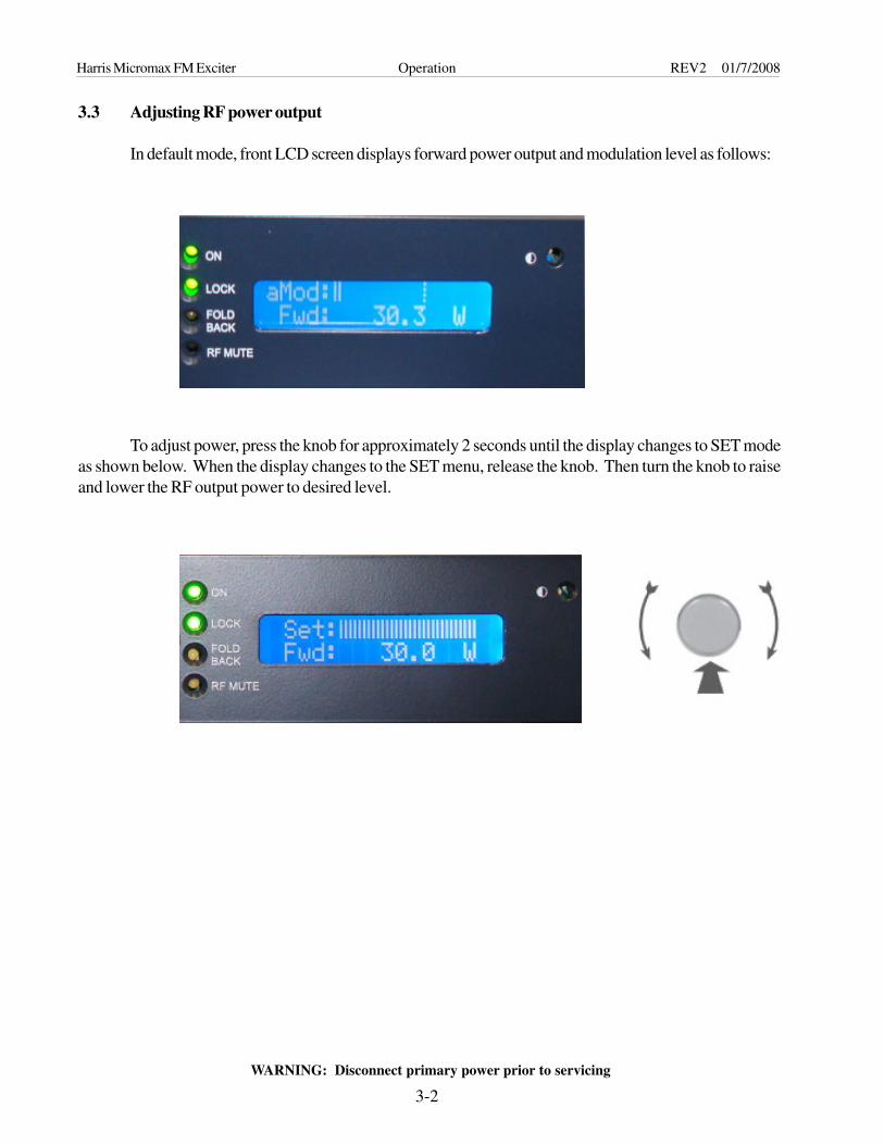
3.3 Adjusting RF power output
In default mode, front LCD screen displays forward power output and modulation level as follows:
To adjust power, press the knob for approximately 2 seconds until the display changes to SET mode
as shown below. When the display changes to the SET menu, release the knob. Then turn the knob to raise
and lower the RF output power to desired level.
Harris Micromax FM Exciter Operation REV2 01/7/2008
3-3
WARNING: Disconnect primary power prior to servicing
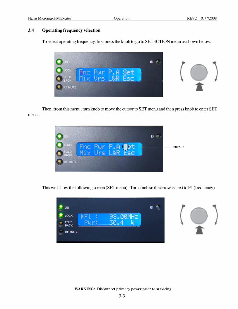
3.4 Operating frequency selection
To select operating frequency, first press the knob to go to SELECTION menu as shown below.
Then, from this menu, turn knob to move the cursor to SET menu and then press knob to enter SET
menu.
This will show the following screen (SET menu). Turn knob so the arrow is next to F1 (frequency).
cursor
3-4
WARNING: Disconnect primary power prior to servicing
Harris Micromax FM Exciter Operation REV2 01/7/2008
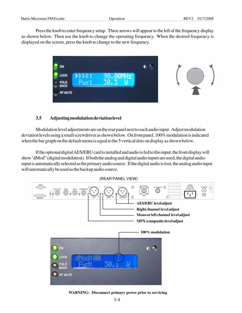
Press the knob to enter frequency setup. Three arrows will appear to the left of the frequency display
as shown below. Then use the knob to change the operating frequency. When the desired frequency is
displayed on the screen, press the knob to change to the new frequency.
3.5 Adjusting modulation deviation level
Modulation level adjustments are on the rear panel next to each audio input. Adjust modulation
deviation levels using a small screwdriver as shown below. On front panel, 100% modulation is indicated
when the bar graph on the default menu is equal to the 5 vertical dots on display as shown below.
If the optional digital AES/EBU card is installed and audio is fed to this input, the front display will
show ‘dMod” (digital modulation). If both the analog and digital audio inputs are used, the digital audio
input is automatically selected as the primary audio source. If the digital audio is lost, the analog audio input
will automatically be used as the backup audio source.
PILOT OUT SCA2 SCA1 COMPOSITEF
W
D
T
LM
E
X
T
A
GC
RS232
REMOTELEFT RIGHT AES/EBU
50O
RF OUTPUTRF SAMPLE
MAINS VOLTAGE
100-250 VAC3.15A SB
MAINS FUSE
L R
MPX (composite) level adjust
Mono or left channel level adjust
Right channel level adjust
(REAR PANEL VIEW)
AES/EBU level adjust
100% modulation
Harris Micromax FM Exciter Operation REV2 01/7/2008
3-5
WARNING: Disconnect primary power prior to servicing
3.6 Front panel LCD display menu description
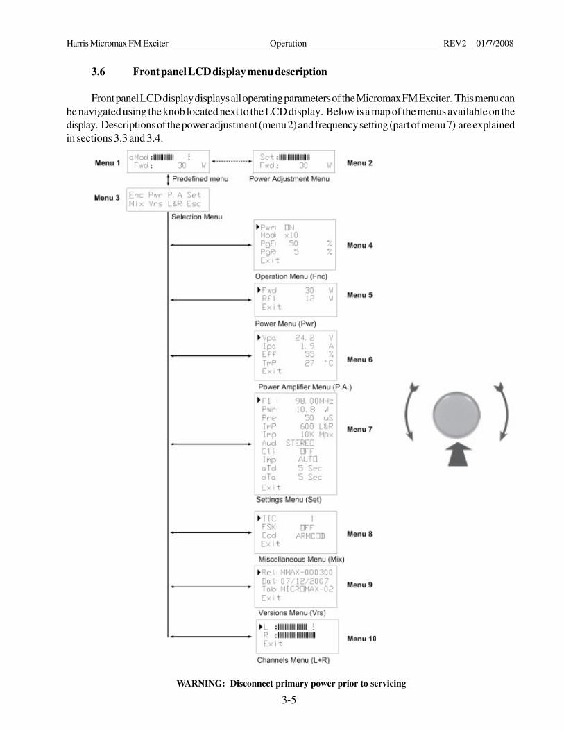
Front panel LCD display displays all operating parameters of the Micromax FM Exciter. This menu can
be navigated using the knob located next to the LCD display. Below is a map of the menus available on the
display. Descriptions of the power adjustment (menu 2) and frequency setting (part of menu 7) are explained
in sections 3.3 and 3.4.
3-6
WARNING: Disconnect primary power prior to servicing
Harris Micromax FM Exciter Operation REV2 01/7/2008
3.6.1 Operations menu (menu 4 - Fnc)
This menu contains the control function to turn on and off the exciter, ability to change the
modulation meter on the LCD display to 10X modulation level and the ability to set PgF and PgR levels.
PgD and PgR are threshold levels that provide a logic high or low state on the telemetry connector. PgD is
a threshold level for the forward power level and PgR is a threshold level for reflected power. For example
if PgD is set at 50%, logic level on pin 7 will change state (high or low depending on jumper settings on the
telemetry board) when forward power is above 15 Watts.
3.6.2 Power menu (menu 5 - Pwr)
This menu indicates forward and reflected power of the exciter.
3.6.3 Power amplifier (menu 6 - P.A)
This menu indicates the PA voltage, PA current, PA efficiency and PA temperature.
3.6.4 Settings menu (menu 7 - Set)
This menu is used to set the operating frequency of the exciter (see section 3.4), turn the audio
clipper on/off, set impedance of audio input (10K or 600 ohms) and turn on/off internal stereo generator
(Aud: STEREO/MONO).
If the optional AES/EBU card is installed, this menu is also used to select the audio input (Inp:
ANALOG/DIGITAL/AUTO). In auto mode, the digital audio input has priority. If the digital audio input is
lost, the analog input is automatically used as the alternate audio source. In the AUTO mode, there are 2
selectable time delays (aTd - analog to digital and dTa - digital to analog). These are the time delays the
exciter will wait until it switches to the alternate audio source.
3.6.5 Miscellaneous menu (menu 8 - Mix)
This menu allows to change the address of the exciter’s IIC bus address, turn on/off FSK and
displays the FSK code.
3.6.6 Versions menu (menu 9 - Vrs)
This menu indicates the version and the release of the software used in the exciter.
3.6.7 Channels menu (menu 10 L&R)
This menu indicates the modulation level of the left and right channel audio levels when the exciter is
operated in the stereo mode using the internal stereo generator.
Harris Micromax FM Exciter Operation REV2 01/7/2008
3-7
WARNING: Disconnect primary power prior to servicing
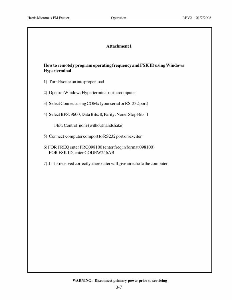
How to remotely program operating frequency and FSK ID using Windows
Hyperterminal
1) Turn Exciter on into proper load
2) Open up Windows Hyperterminal on the computer
3) Select Connect using COMx (your serial or RS-232 port)
4) Select BPS: 9600, Data Bits: 8, Parity: None, Stop Bits: 1
Flow Control: none (without handshake)
5) Connect computer comport to RS232 port on exciter
6) FOR FREQ enter FRQ098100 (enter freq in format 098100)
FOR FSK ID, enter CODEW246AB
7) If it is received correctly, the exciter will give an echo to the computer.
Attachment 1
1
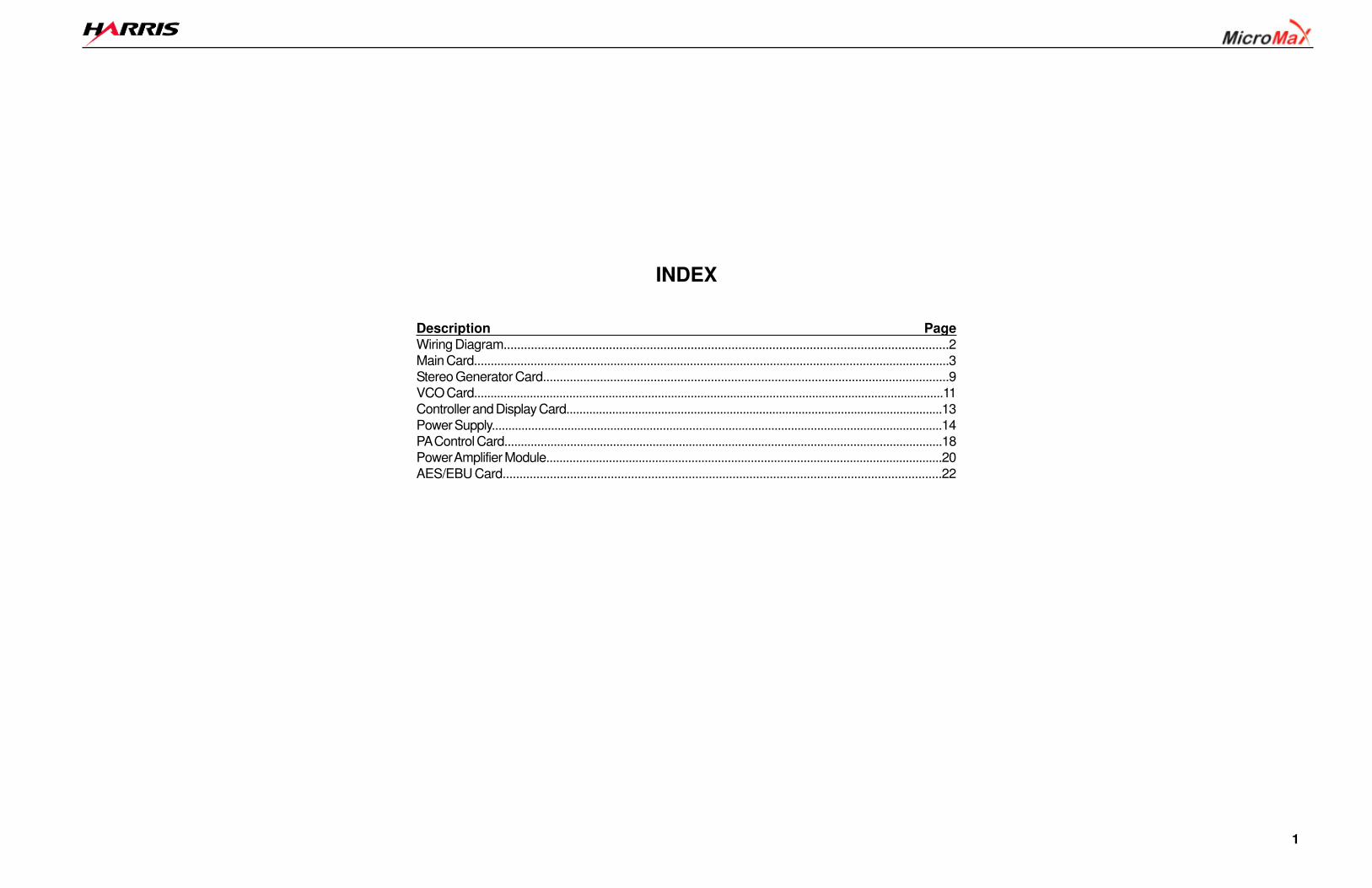
INDEX
Description Page
Wiring Diagram...................................................................................................................................2
Main Card...............................................................................................................................................3
Stereo Generator Card.........................................................................................................................9
VCO Card...............................................................................................................................................11
Controller and Display Card...................................................................................................................13
Power Supply.........................................................................................................................................14
PA Control Card.....................................................................................................................................18
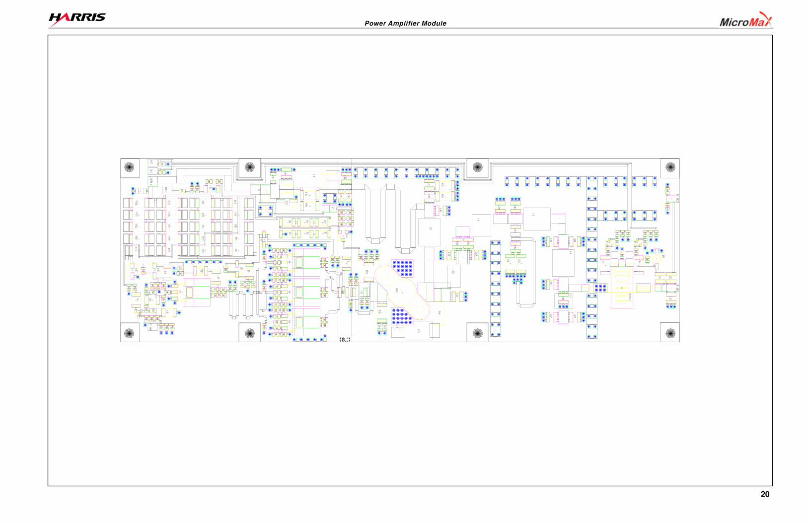
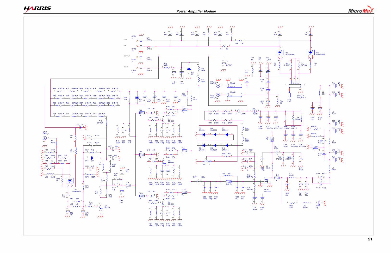
Power Amplifier Module........................................................................................................................20
AES/EBU Card..................................................................................................................................22
2
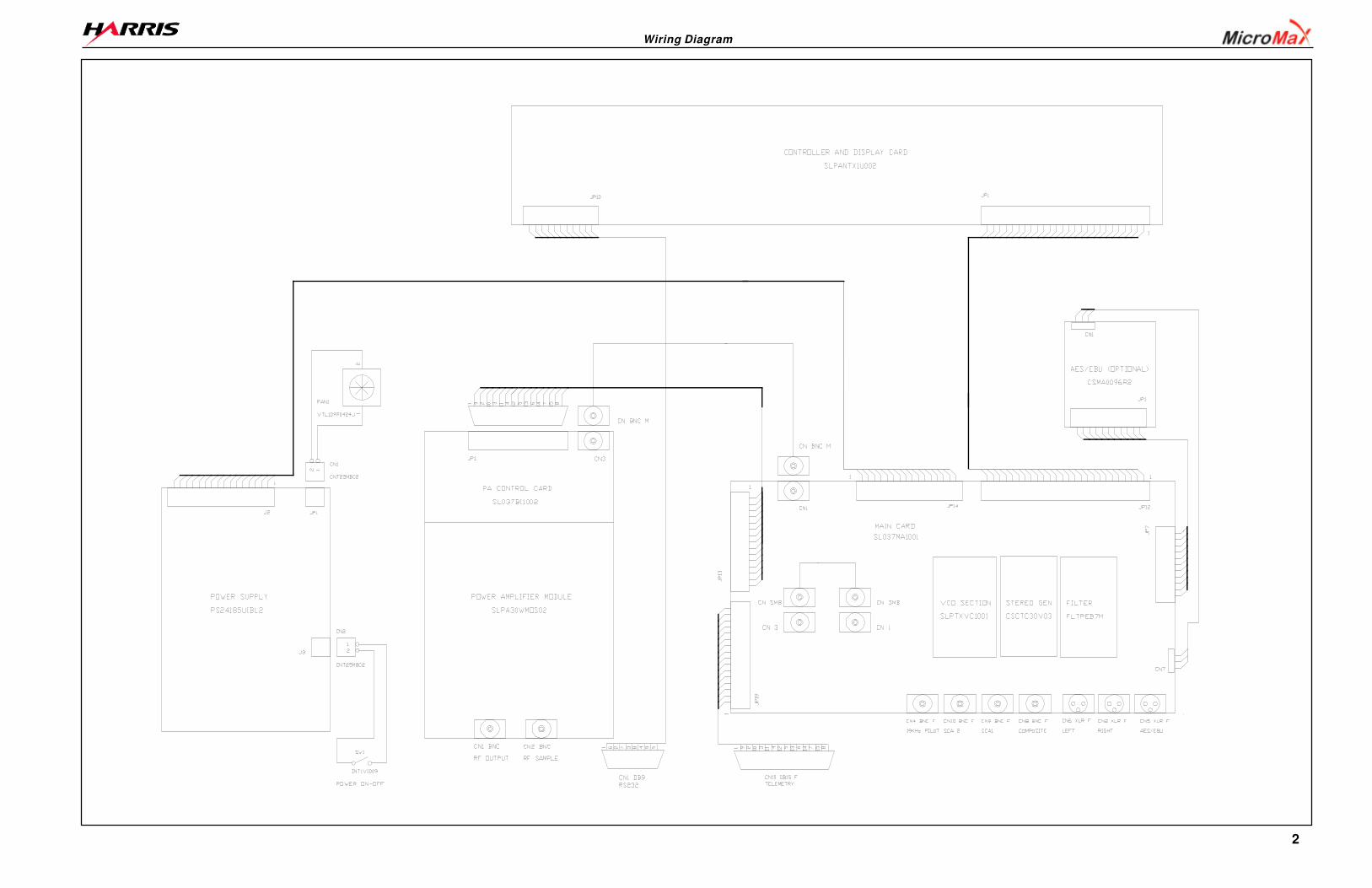
Wiring Diagram
3
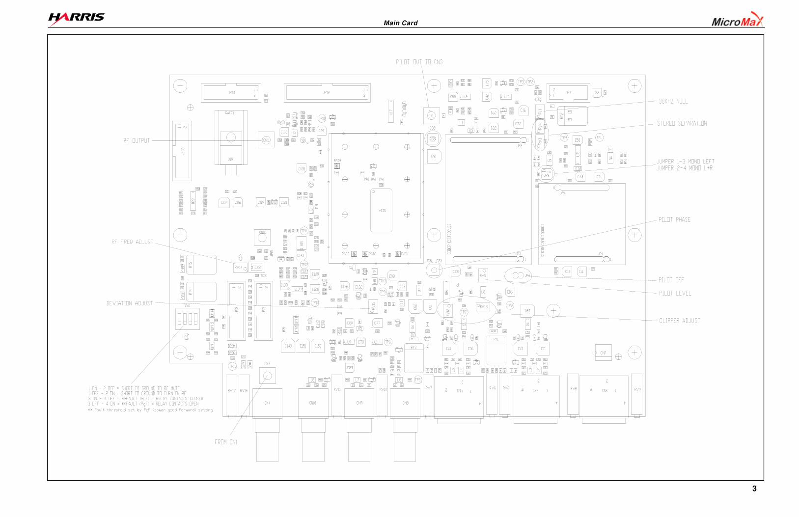
Main Card
4
V5V15
50US
ONRLEV
OFF
75US
PGOOD
INTLK
CLIPP
EXTAGC
GNDH
FWD
STEREO
RFL
IPA
V15
VPA
ON
SDA
OFF
SCL
V5
PGOOD
VSS
V5
V15
INTLK
GND
GND_A
EXTAGC
GND_T
1
FIX18FIX35
FWD
V18
IPA
VPA
RFL
EXTAGC
IPA
CPULK
GND
INTLK
600CMD
DATA
EN2
SDA
IN1
GN
D2
FX
4
OUT3
U19 LM7815
CLK
50CMD
V18
1
FIX16FIX35
1
FIX15FIX35
1
FIX14FIX35
1
FIX13FIX35
1
FIX12FIX35
1
FIX11FIX35
MODx10
SDA PGOOD
FWD
VPA
SCLOFF 1 23 45 67 89 1011 1213 1415 1617 1819 2021 2223 2425 26
JP12CN26PD
REMOFF
SCL
V5
RIGHTRFL
ON
MOD
LE
CPUOFF PWALOCK
EN1CLOCK
LEFT
50US
DATA-P
RAFF1RAFF220A
CPUOFF
75USCLIPP
TEMP
1
FIX17FIX35
1
FIX19FIX35
VPA
12
+
C11410uF/35V
1 23 45 67 89 1011 1213 1415 16
JP14
CN16PD
Power Supply
12
C1180.1uF
GND
1 23 45 67 89 1011 1213 1415 16
JP13
CN16PDTo PA
VA
V5STEREO
LIM
QUICK
12
+
C11610uF/16V
12 C115
0.1uF
12
C1170.1uF
DIGI-ON QUICKDIGI-ON
To Panel
V15
DIGI-OK
1 2R141 10K2
1 2
R142 NC
600CMD
12
R1431K13
V5
STR1
D2
CLK3
OE15
Q14
Q25
Q36
Q47
Q514
Q613
Q712
Q811
QS9
QS10
U17
CD4094SMDLLEV
50CMD
MODx10
VDD2
V18
MODLEV
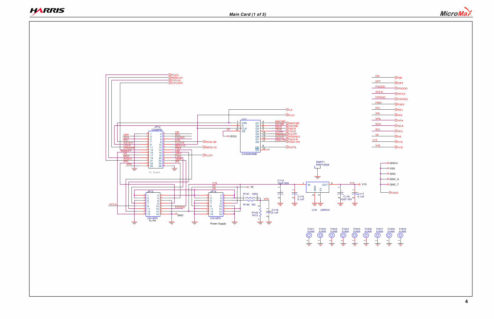
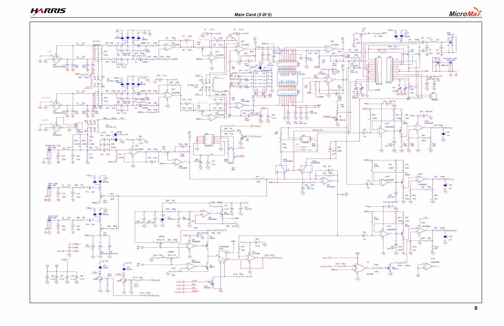
Main Card (1 of 5)
5
GND
VTUNE
12
R123
4K70
12
R131NC
1 2
C105 NC
1 2R137 27H0
12
+ C10310uF/16V
1
2 345
CN11
SMB_CS
FIX10
FIX22
12
C104 NC
12
C112
10pF
TP10NC
L10
18uH
1 2R1191K20
1 2R1211K20
12
R124
NC
1 2R127 27H0
FIX7
FIX22
FIX8
FIX22
1 2R126 82H0
1 2
C110 27pF
12
R118
NC
3
21
D Q15
NC
12
R134
330H0
1 2
C111 27pF
12
R135
330H0
FIX2
FIX22
V1
G3
G5
MOD7
VT8
G6
G4
RF2
VCO1 NC
1 2R128 8H2
1 2R1171K20
12
C101
10nF
12
R122
2K0
1 2R129 8H2
21
DL1
LED-G0805
FIX9
FIX22
FIX4
FIX22
12
+C10210uF/16V
L12
2u2
12
+ C10810uF/16V
12
R133
120H0
FIX5
FIX22
1PAD
PAD1
1PAD
PAD2
1 2R115 NC
12
+ C9810uF/16V
1PAD
PAD3
FIX1
FIX22
1PAD
PAD4
FIX6
FIX22
12
R120
6K80
12
C970.1uF
L11 2u2
3
2
1
4
Y2
MAR6SM1
2 3
Q13BC847
L9
18uH
12
+ C9910uF/16V
12
C96
NC
FIX3
FIX22
L13 47nH
12
C107
1nF
1
2 3
Q14BC847
TP9NC
1 2
R125 NC3
2
1
4
Y1ERA3SM
12
C109
1nF
1 2
C1061nF
1 2R116 1K20
12C100
10nF
1 2R138 22H0
1 2R136 82H0
12
C113
10pF
12
R130
NC
12
R139
27H01
2
R132
22H0
GND
V15
V15
A
A
A
A A
A
A
A
A
A
A
A
A
A
A
A
A
A
A
A
A
AA
AAA
A
AAAAAA A
V15
RFOFF
AFGND
AFTUNE
A
RFPLL
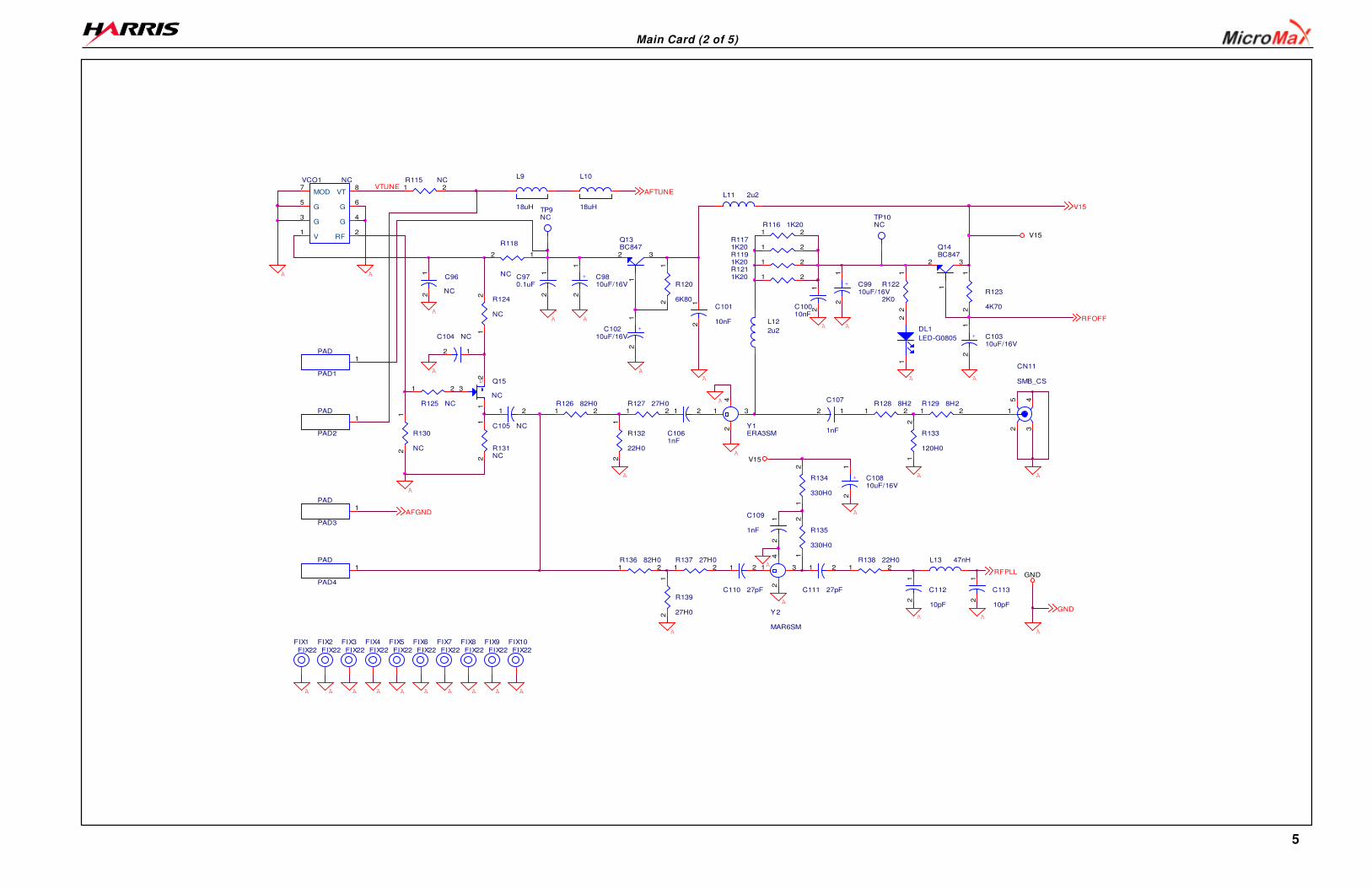
Main Card (2 of 5)
6
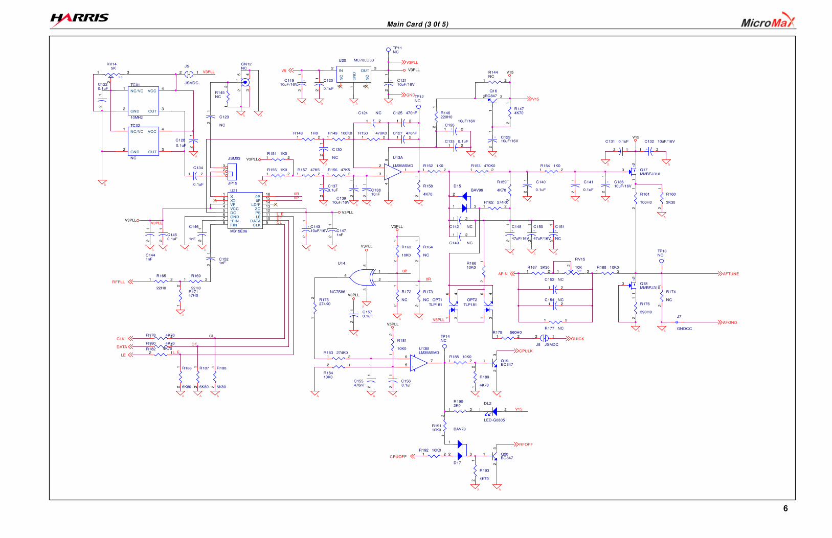
Main Card (3 0f 5)
DTL_E
CL
L_E
CL
V5PLL
V15
0P0R
0P1
24
53
U14
NC7S86
12
J8 JSMDC
CPUOFF
1 3
2
cw
RV145K
DT
V3PLL
1 2
R1902K0
V3PLL
12
R186
6K80
5
67
+
-
U13BLM358SMD
12
R188
6K80
12
R163
10K0
12
R1474K70
1 2R157 47K5
12
R175274K0
12
R145NC
1 2R156 47K5
NC/VC1
GND2
OUT3
VCC4
TCX1
10MHz
12
R161
100H0
1 2R183 274K0
12
+C11910uF/16V
12
C1471nF
1 3
2
D15BAV99
12
C1370.1uF
1 2R165
22H0
12
R164
NC
12
C120
0.1uF
1
23
Q20BC847
1 2C133 0.1uF
12
C1441nF
1 2R179 560H0
12
R17147H0
TP11NC
12
C1560.1uF
2 3
1
D17
BAV70
123
JP15
JSM03
1 2+
C12610uF/16V
12
+
C13910uF/16V
1 2R169
22H0
12
C155470nF
TP12NC
1 2R167 3K30
1 2R192 10K0
XI1
XO2
VP3
VCC4
DO5
GND6
*FIN7
FIN8
CLK9DATA10LE11PS12ZC13LD/F140P150R16
U21
MB15E06
12
+ C14310uF/16V
12
C13810nF
12
+C150
47uF/16V
TP14NC
1 3
2
cw
RV15
10K
12
R19110K0
1 2
C125 470nF
12
C128
0.1uF
12
R146220H0
GND
12
C1570.1uF 1 3
46
OPT1
TLP181
12
C123
NC
1 2
C153 NC
12
C1220.1uF
1 2
R177 NC
12
R193
4K70
1 2C127 470nF
12
C1521nF
J7
GNDCC
1 2R148 1H0
1 2R152 1K0
12
J5
JSMDC
12
+C151
NC
12
R181
10K0
1 2C154 NC
1 346
OPT2
TLP181
1 2
C142 NC
NC/VC1
GND2
OUT3
VCC4
TCX2
NC
12
C146
1nF
12
R172
NC
1 2R153 470K0
1
2 3
Q16
BC847
12
R18410K0
1
2 345
CN12NC
12
R16610K0
1 2R149 100K0
1 2R154 1K0
12
C1450.1uF
1 2R155 1K0
IN2
NC
4
NC
5
GN
D1
OUT3
U20 MC78LC33
1 2R150 470K0
1 2R151 1K0
12
C140
0.1uF
1 2R185 10K0
1 2R168 10K0
21
DL2
LED-G0805
1 2
C149 NC
12
R159
4K70
3
21
D
Q17MMBFJ310
12
+ C12110uF/16V
12
R189
4K70
12
R160
3K30
1
23
Q19BC847
1 2
C134
0.1uF
1 2R162 274K0
TP13NC
3
21
D
Q18MMBFJ310
12
R158
4K70
1 2
R144NC
12R182 4K70
12
+ C12910uF/16V
1 2
C124 NC
12
R176
390H0
12
R173
NC
12
C141
0.1uF
1 2R180 4K70
1 2+
C132 10uF/16V
3
21
48
+
-
U13A
LM358SMD
12
C131 0.1uF
12
+ C13610uF/16V
1 2R178 4K70
12
C130
NC
12
+C148
47uF/16V
12
R174
NC
12
R187
6K80
V15
V5PLL
V15
V3PLL
V3PLL
V3PLL
V3PLL
V3PLL
V3PLL
V3PLL
AA
A
A
AAA A
AAA
A
A
AA
AA AA
A
A
A
A
AA
AA
AA A A
A
A A
A
A
A
A
A
AA
AA
A
AA
A
V5
A
A
V3PLL
V15
CLK
RFPLL
LE
DATA
AFTUNEAFIN
QUICK
AFGND
RFOFF
CPULK
0R
7
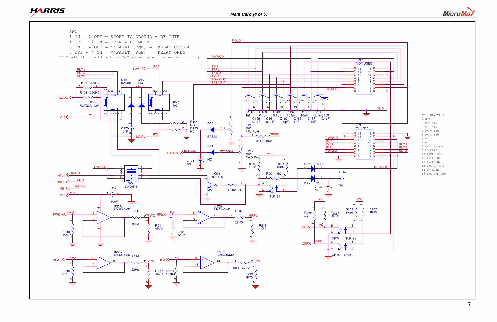
Main Card (4 of 5)
PWRGD
FWD
1234
8765
SW1SWDIP4
RFL
IPA
V18
PWRGD
TRFL
TIPATVPATRFL
VPATIPA
FWADJ
TVPA
RLY3
V18 DB15 REMOTE 2
1 GND
2 FWD Tlm
3 RFL Tlm
4 PA V Tlm
5 PA I Tlm
6 FAULT
7 NC
8 EXCITER APC
9 RF MUTE
10 INTLK COM
11 INTLK NC
12 INTLK NO
13 EXC ON CMD
14 RF MUTE
15 EXC OFF CMD
RLY2
EXTAGC
TVPA
RLY1
12
R2091K80
12
R2174K70
12
C17010nF
12
R216NC
21
D19NC
12
C1690.1uF
3
21
411
+
-
U22ALM324SMD
12
R2001K80
21
D21
NC
13
2
cw
RV1620KRFL Fold
12
C1711nF
2 1D22 BAS32
21
D20
BAS32
SDA
12
C1600.1uF
12
R2044K70
12
C16610nF
12
R210100K0
1 2R198 330H0
12
C1581nF
12
R2114K70
13
2
cw
RV1720KFWD Fold
12
C1610.1uF
12
C172NC
1 2
R206
22H0
12
C164100pF
1
34
6
OPT4 TLP181
1 2 3 4 56789
10
+
-
RY5NC
12
R2084K70
12
C1680.1uF
1 2 R195NC
1 23 45 67 89 1011 1213 1415 16
JP19CN16PD
1 2 3 4 5678910
+
-
RY4RLTQ2A_12V
1 2
R207
22H0
12
R2051K80
12
1314
+
-
U22DLM324SMD
1 2
C173
10nF
12
R1991K80
1 2
R215 22H0
1 2
R196 0H0
10
98
+
-
U22CLM324SMD
12
R2134K70
1
34
6
OPT5 TLP181
12
C163100pF
TP15
NC
12
R2194K70
2 1
D23 NC
12
C1620.1uF
1 2R197 330H0
12 R212
100K0
21
D18BAS32
1 2R201 NC
1 23 45 67 89 1011 1213 1415 16
JP18NOT USED
12
C1590.1uF
12
R218100K0
1
32
Q21BCR135
12
C1670.1uF
12
C1651nF1 2 R194
NC
5
67
+
-
U22BLM324SMD
1
34
6
OPT3TLP181
1 2
R214
22H0
1 2
R202 0H0
PGOOD
V18
SCL
SDA
GND
V15
V5
GND
EXTAGC
INTLK
VPA
FWD RFL
IPA
ON
OFF
INTLK
OFF
GND
TIPA
V5
TRFL
TFWD
V18
FOLD1
ON
RF-MUTE
SCL-OUT
FWADJ
V5
TFWD
PWRGD
RF-MUTE
SW1
1 ON - 2 OFF = SHORT TO GROUND = RF MUTE
1 OFF - 2 ON = OPEN = RF MUTE
3 ON - 4 OFF = **FAULT (PgF) = RELAY CLOSED
3 OFF - 4 ON = **FAULT (PgF) = RELAY OPEN
SDA-OUT
SCLSCL
** Fault threshold set by PgF (power good forward) setting
V15
RLY1RLY3
TFWD
RLY2V18
8
Main Card (5 0f 5)
Left/Mono
Right
50H
V15
MODX10
STEREO
CLIPP A
12
+
C82220uF/16V
VREF
75U
GND
50U
PRE-R
V5INT
PRE-L
75U
1 2R89 1K0
12
R109
1M0
1 2R86 1K0
3
21
48
+
-
U7ATL072SMD
5
67
+
-
U12B
LM358SMD
123456 7 8 9
10
+
RY2
RLTQ2A_12V
12
R50
100K0
1234567891
0
JP1NC
1
23
Q5BC847
12
+ C4810uF/16V
9
4
53
1 0
U16CCD4053SMD
12
R113
4K70
1 2
C71 10nF
12
C74
27pF
12
C58
0.1uF
12
C4527pF
1
23
Q6BC857
1 2R69 2K49
12
C1 0.1uF
TP7NC
V15
12
+C50
10uF/16V
1 2
R108
10K0
1234567891011121314
JP2
STF14S
1
23
Q10BC847
12
R61
150H0
13
2
cw
RV310K
1 2R105 47H0
TP4NC
1
23
Q4BC857
12R53 150H0
13
2
cw
RV12 5K
UPPER
1 2
R1 100K0
1 2R83
49K9
12
R85
2K0
12
R91100K01 2
C79 10nF
12C271nF
12
R71
10K0
13
2
cw
RV11
10K
1 2
R56 0H0
12
+
C8910uF/16V
1
32Q12
BCR135
12
C1727pF
12
C94
0.1uF
1 2R77
10K0
1 2R110 10K0
1 2+
C78 10uF/16V
1 2
R28 150H0
STEREO_INT
5
67
+
-
U8BLM358SMD
1 2
C14100pF
12
R64
10K0
L1 2u2
STEREO
21
D14
BAS32
L6 2u2
L5 2u2
1 2
R702K49
1 2+
C42 10uF/16V
1 23 45 67 89 10
JP7
CN10PD
1 2
C39 47pF1
2
R14
10K0
12
+C68
10uF/16V
1 2 R1030K9
TP6NC
1 2
C88
0.1uF
L3 2u2
V15
1 2
C85
1uF
12
C1827pF
12
C52
0.1uF
1 2R79 100H0
L4 2u2
12
C95
0.1uF
12
C25 0.1uF
1
32
Q3NC
21
D12
5V1
12
+
C2810uF/16V
12
C67
0.1uF
12
R5710K0
1 2R13 NC
12
R25
NC
13
2D7 BAV99
12
R74
100K0
3
1 2
4
CN5
XLRFNC3H
13
2
cw
RV7
10K
1
23
Q8BC847
12
R44
10K0
5
67
+
-
U5BTL072SMD
12
R1032K0
1 2+
C55 10uF/16V
600H
12
+ C8010uF/16V
13
2
D11
BAV99
1 2
R30 150H0
A11
A24
A38
A411
C1
13
C2
5
C3
6
C4
12
VDD14
VSS7
B12
B23
B39
B410
U15 CD4066XSMD
12
C83
27pF
1 2R7 20K0
12
C240.1uF
1 2R41 30K9
12C35 0.1uF
TP1NC
TP2NC
1 2R20 10K0
21 3
C326-30pF
5
67
+
-
U6BTL072SMD
1 2
C15150pF
1 2
C49100pF
1 2
C69 NC
12C9
27pF
1 3
2
cw
RV1
5K
12
+
C41 100uF/16V
1 2+
C1610uF/16V
1 2 3 4 5 6 7 8 9 10
JP4NC
12
C19 0.1uF
1 2R66 1K0
1 2C4 15pF
12
R67
28K0
12
C64
27pF
1 2R29 10K0
SCA2 - CN10BNC_IS90
1 2 C59
470nF
3
21
48
+
-
U8ALM358SMD
123456789
10111213
JP3
STF13S
13
2
D1BAV99
3
21
48
+
-
U12A
LM358SMD
RLEV
12 C8
27pF
12
+
C13 100uF/16V
12
+
C7 100uF/16V
1
23
Q11BC847
21D4 5V1
1 2R43 20K0
12
R102
12K1
1 2R17 10K0
1 2
R94 1K0
12
R1114K70
1 2
C61 10nF
10
15
2 1
10
U16BCD4053SMD
13
2
D3
BAV99
12C231nF
1 2R99 4K99
12
C4627pF
12
R39
10K0
12
C290.1uF
12
R6520K0
12
R73100K0
5
67
+
-
U1BTL072SMD
1 2
R15 10K0
12
R371K20
11 22 33
CN7CN03PS
21
D8
5V1
DIG-L
12
C5 0.1uF
1 2
R106 576H0
1 2R80 1K0
1 2 3 4 567891
0+
RY1
RLTQ2A_12V
1 2R33 20K0
12
R381K20
12
+
C91220uF/16V
12 C261.5nF
123456 7 8 9 1
0
+
RY3RLTQ2A_12V
1
2 345
CN1SMB_CS
L8 2u2
12
C4427pF
12
+
C7510uF/16V
12
+
C36 100uF/16V
L7 2u2
1 2R107 10K0
AFIN
TP8NC
12
R401K0
PILOT OUT - CN4BNC_IS90
12
C93
0.1uF
21
D13
BAS32
1 2
C370.1uF
12R23 10K0
12
C4327pF
21 3
DZ1LM4040-10
1 2C63 15pF
12
R75
10K0
1 2R58
10K0
12
R60
150H0
1 2R16 NC
V15
1 2
R48 48K7
21
D10
5V1
1 2
R54 NC
INA
1
GN
D2
GN
D3
-V4
GN
D5
GN
D6
OU
TA
7
GN
D8
GN
D9
+V
10
INB
11
GN
D1
2G
ND
13
-V1
4G
ND
15
GN
D1
6O
UT
B1
7G
ND
18
GN
D1
9+
V2
0
HY1
FIL19KS
5
67
+
-
U11B
LM393SMD
12
C76
0.1uF
12
R84
12K1
1 2
R3110K0
12
R101
10K0
5
67
+
-
U2BTL072SMD
12
R82
10K0
12
R72
470K0
13
2
D9
BAV99
LLEV
21 3
C31
6-30pF
13
2
cw
RV2
10K
50H
1
234 5
CN3
SMB_CS
12
C2 0.1uF
12
C2127pF
13
2
cw
RV5
50K
12
C84
27pF
A
600H
12
R93
10K0
13
2
cw
RV13 5K
LOWER
5
67
+
-
U4B
TL072SMD1
2
C92
0.1uF
12
C900.1uF
12
C33NC
12
+ C7210uF/16V
13
2
D6BAV99
1 2
R42 10H0
V15
12
C34NC
1 2R18 30K9
1 2
R96 1M0
1 2
C38150pF
1 2R97 100H0
5
67
+
-
U7BTL072SMD
5
67
+
-
U9BLM358SMD
1 2R104 15K0
1 2
R19 10H0
DIG-R
12
R59
150H0
1 2
C3 47pF
12
R6210K0
1 2R21
48K7
12
R52
10K0
5
67
+
-
U10B
LM393SMD
13
2
cw
RV10
10K
12
R12
1K20
12
R11
1K20
116
14
12
1310
U16A
CD4053SMD
COMPOSITE - CN8
BNC_IS90
1 2R81 10K0
1 2R114 10K0
1 2R6 10H0
12J3 JSMDC
1 2R5 100H0
1 2R112 10K0
PRE-L
1 2+
C2210uF/16V
12
R45NC
1 2R47 2K0
1
23
Q2BC857
12
+
C1110uF/16V
12
R632K0
3
21
48
+
-
U5ATL072SMD
12
R51
100K0
1 2R95 49K9
1 2
C70
1uF
1 2
C40 15pF
12C6 0.1uF
1
23
Q7BC857
1
32
D
Q92N7002
1 2R9 2K0
3
21
48
+
-
U4A
TL072SMD
1 23 4
JP8
STM04D
12
J4 JSMDC
1 2
C57 470nF
12
R261K0
13
2
cw
RV920K
JP
1-3 MONO L
2-4 MONO L+R
3
1 2
4
CN2
XLRFNC3H
SCA1 - CN9BNC_IS90
12 C60
NC
1 2R88 4K99
1 2R27 1K0
12
R100
10K0
1 2
C56
1uF
MODLEV
13
2
cw
RV6
10K
1 2R46 4K12
1 2
C66 47pF
12
+
C6210uF/16V
3
21
48
+
-
U1A
TL072SMD
1 2R24 20K0
1 2
R8 4K12
12
R3510K0
12
C2027pF
13
2
D2BAV99
3
21
48
+
-
U11A
LM393SMD
12
+
C5110uF/16V
12
R92
100K0
1 2R22
10K0
13
2
cw
RV410K
12
R34NC
1 2R98 10K0
1 2+
C86 10uF/16V
1 2R32 10H0
1 2 R3630K9
12
C73
27pF
TP3NC
3
1 2
4
CN6
XLRFNC3H
12
C47 0.1uF
1 2
R78 10K0
TP5NC
1 2R2 10K0
DIGI-OK1
3
2
D5BAV99
12
JP6
STM02S
12
R3
100K0
3
21
48
+
-
U10A
LM393SMD
3
21
48
+
-
U2A
TL072SMD
12
+ C7710uF/16V
1 2R55 100H0
12
+
C1210uF/16V
12
R90
15K0
12
+
C81220uF/16V
12
C530.1uF
12
C100.1uF
1
24
53
U3
NC7S86
1 2
R87 100H0
12J1 JSMDC
3
21
48
+
-
U6A
TL072SMD
12
C540.1uF
12
R6812K1
13
2
cw
RV820K
1
32
Q1
BCR135
3
21
48
+
-
U9A
LM358SMD
1 2R76 10K0
12
J2 JSMDC
1 2R4 NC
L2 2u2
1 2R49 10K0
12 C301.5nF
12
C65
27pF
VREF
V15
VREF
VREF
VREF
VREF
V15
VREF
VREF
V15
VREF
V15
ADJ -14/+14
ADJ -14/+14
V15
VREF
V15
VREF
VREF
VREF
V15
VREF
V15
V15
V15
V15
V15
VREF
V15
V15
V15VREF
V15
VREF
V15
V15
V15
V15
V15
V15A
A
A
A
A
A
A
A A
A
A A
A
A
A
A
A
A
A
A
A
A
A
A
A
A
AA
A
A
A
AAA
A A A
A
A
A
A
A
A A
A A
A
A
A
A
A
A
A
A
A
A
AA
A
A
A
A
A
A
A
A
AA
A
A
A
A
AA
VSS
A
A
A
A
VDD
A
A
VEE
DIGI-ON
V3PLL
A
A
A
V3PLL
AA
V15
V15
A
V15
A
AA
AES/EBU
V15
A
A
V15
A A
VREF
A
A
A
VREF
VREF
A
V15
A A
A
A
AA
A
PRE-R
600CMD
V15
CLIPP
50CMD
75US
50US
STEREO
V3PLL
VREF
V15
DIGI
50UDIG-L
V5INT
12
+
C87220uF/16V
GND_T
DIGI
DIG-R
V15
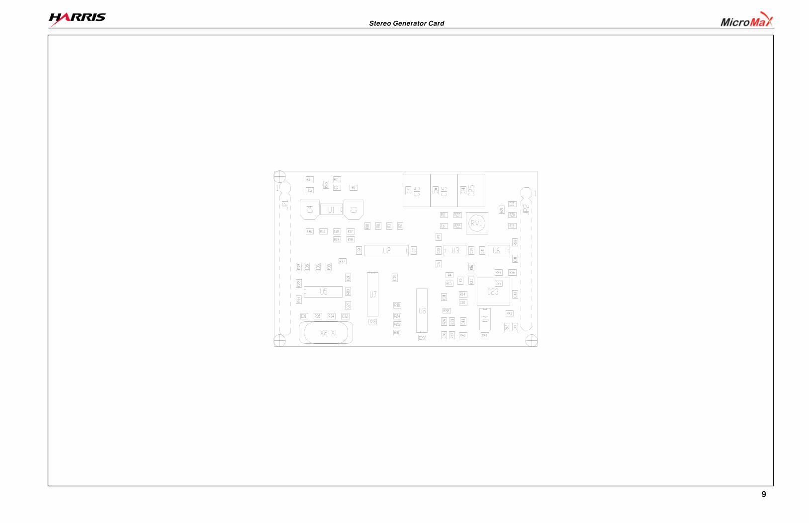
9
Stereo Generator Card
10
123456789
1011121314
JP1
STM14S
5
67
+
-
U4BTL072SMD
1 2R7 4K75
1 2R13 4K75
1 2
R43
22H0
12
R302K10
12
R311K0
1 2
R12
2K74
1 2
R62K74
12
R32825H0
12
R241K33
12
R252K49
12
R263K30
12
R331K74
12
C340.1uF
12
C330.1uF
12C26
NC
+
C1
10uF 16V
+
C4
10uF 16V
VDD
VSS
VSS
VDD
12
R22
2K15
1 2
C50.1uF
12
R271K69
3
21
48
+
-
U6A
LM833/SO
12 C20
2.2nF 1%
VSS
12
R1
100H0
1 2
R17
100H0
1 2
R18
1K07
1 2
R21K07
12
R3
1K50
12
C24220pF 1%
12
R8
2K10
12
R101K50
12
C290.1uF
VDD
12
C300.1uF
12
C70.1uF
12
C80.1uF
5
67
+
-
U6BLM833/SO
VDD
1 2
R28
1K20 1 2R291K33
VSS
1 2C22 1nF 1%
12
R44100K0
VDD
12
R451M0
1 2
R46 1M0
12345678910111213
JP2
STM13S
12
R2139K0
1 2
C180.1uF
12
C270.1uF
12
C280.1uF
VSSVDD
1 2C104.7pF
1 2
14
7
U5ACD4069/SO
1 2C3
4.7pF
3 4
14
7
U5BCD4069/SO
11 10
14
7
U5ECD4069/SO
5 6
14
7
U5CCD4069/SO
9 8
14
7
U5DCD4069/SO
1312
14
7U5FCD4069/SO
12
C361nF 1%
3
21
48
+
-
U1ALM833/SO
CLK1
CKE2
RST7
Q03
Q14
Q25
Q36
VCC16
GND8
U7A
CD4520/SO
5
67
+
-
U1B LM833/SO
CLK9
CKE10
RST15
Q011
Q112
Q213
Q314
VCC16
GND8
U7B
CD4520/SO
3
21
48
+
-
U4ATL072SMD
12
C16100pF
1 2
R15
6K80
12
R20715K0
12
R3622H0
12
R19715K0
1 2R14 6K80
1 2
C12 10pF
EN6
GND8
A11B10C9
VDD16VEE7
X3
X013 X114 X215 X312 X4
1 X55 X62 X74
U2
CD4051/SO
EN6
GND8
A11 B10 C9
VDD16 VEE7
X3
X013X114X215X312X41X55X62X74
U8
CD4051/SO
VDD
VSS
1 2
R23
3K30
12
C21
56pF
12
C38
0.1uF
1 2
C39
0.1uF
1 2
C40
0.1uF
1 2
C111nF 1%
1 2
C41
0.1uF
1 2
R16
1K07
13
2
cw
RV1500H
12
R34330H0
3
21
48
+
-
U3ALM833/SO
1 2R35
2M20
12
R470H0
VDD
VSS
12
R5
5K60
VDD
1 2
C23
NC12
C25
NC
12
C19NC
VSS
12
C15NC
1 2
R4
5K60
1 2
R9
1K58
1 2
R11 1K50
12
C42
0.1uF
1 2C6 1nF 1%
VDD
X1
4M864X2
NC
12
C3227pF
12
C3127pF
12
C14680pF 1%
VSS
VDD
5
67
+
-
U3BLM833/SO
1 2
R40 22K0
1 2
R41 22K0
12
C43150pF
12
C4415pF1
2
C3510nF
1 2
R38
3K30
12
R39
330H0
12
R3715K0
12
R4222K0
Stereo Generator Card
11
VCO Card
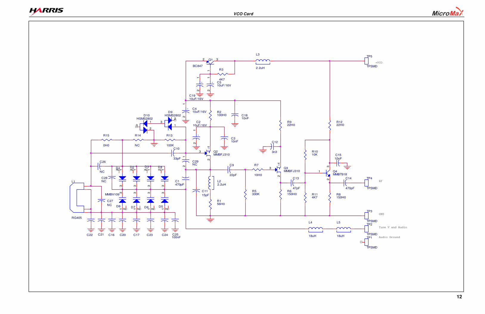
12
Audio Ground
GND
RF
+VCO
Tune V and Audio
TP5
TPSMD
TP4
TPSMD
TP3
TPSMDTP2
TPSMDTP1
TPSMD
C21 C20 C24C23 C25100nF
C22
C1470pF
C26
NC
C27
NC
3
12
D
Q3MMBFJ310
R14
NC
R922H0
R2100H0
C310nF
3
12
D
Q2MMBFJ310
R156H0
C9
22pF
R13
100KC10
33pF
R7
10H0C13
47pF
C15
10nF
C14
470pF
1
23
Q4MMBT918
R8150H0
R1010K
R114K7
R1222H0
R15
0H0
C11
15pF1
2
+
C1910uF/16V
12
+ C510uF/16V
12
+ C410uF/16V
12
+
C210uF/16V
L22.2uH
C28NC
L3
2.2uH
L4
18uH
L5
18uH
1
23
D9HSMS2802
1
23
D10HSMS2802
1
2 3Q1
BC847
R6150H0
C12
3n3
R5330K
R3
4K7
312
D4
312
D3
312
D2
312
D1
MMBV109
31 2
D5
31 2
D6
31 2
D7
31 2
D8
L1
RG405
C1810nF
C16 C17
12
C29NC
VCO Card
13
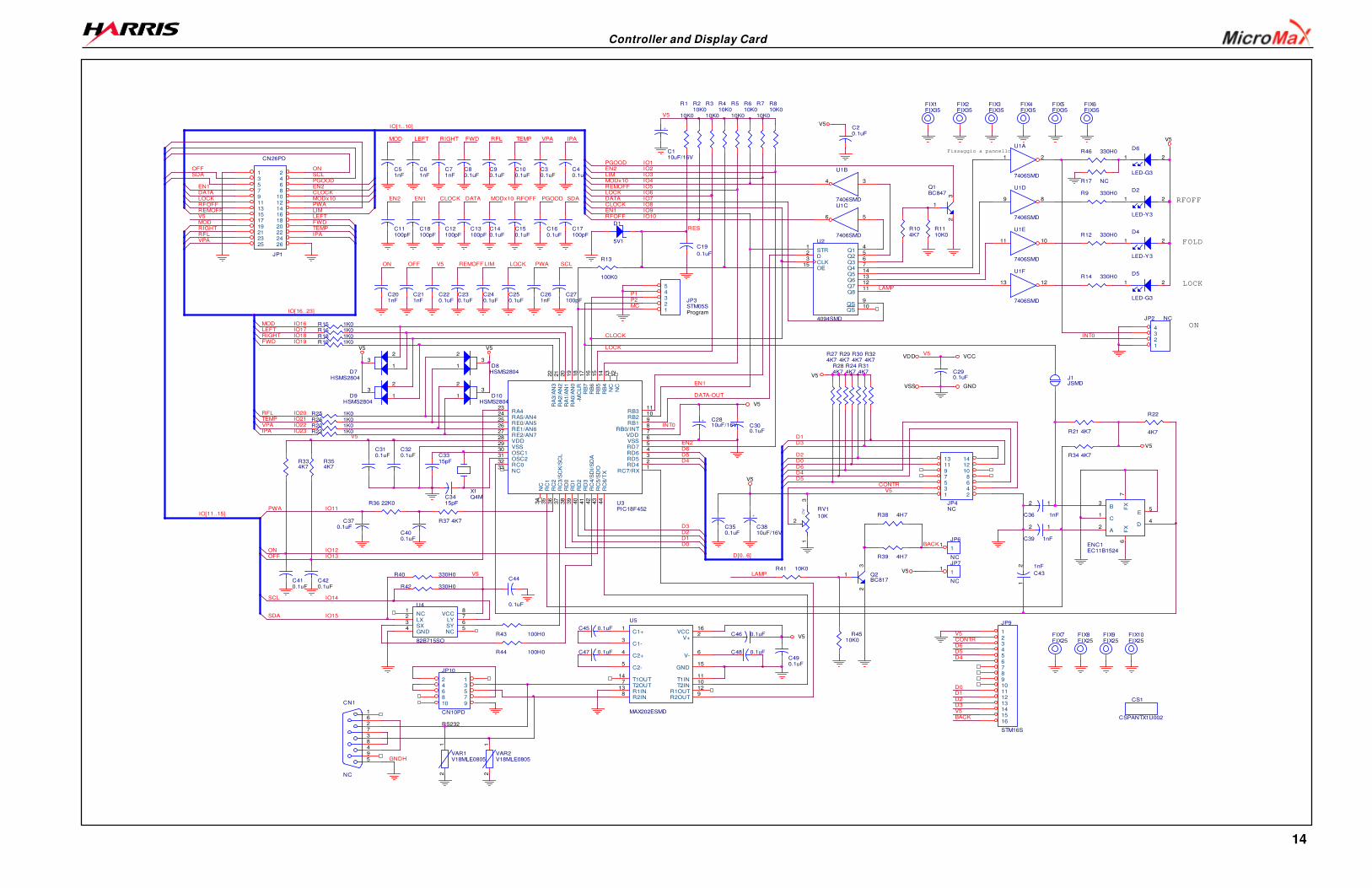
Controller and Display Card
14
SDA
MODx10
IPA
FIX8FIX25
12345678910
JP10
CN10PD
RS232
R36 22K0
C370.1uF
C400.1uF
R334K7
R354K7
PGOOD
OFF
BACK
CONTR
C45 0.1uF
R810K0
FIX9FIX25
IO[16..23]
PWA
C261nF
12345
JP3STM05SProgram
P2
SCL
P1
VPA
MODx10 IO4
C47 0.1uF
FWD
D6
V5
FIX10FIX25
V5
VSS
VDD
V5
V5
V5
V5
GND
VCC
V5
V5
V5
V5
V5
1234
JP2 NC
EN1 IO9
C30.1uF
C100.1uF
C90.1uF
C80.1uF
1
23
D7HSMS2804
C490.1uF
C290.1uF
C40.1uF
C51nF
C71nF
C61nF
C350.1uF
C19
0.1uF
C20.1uF
C310.1uF
C44
0.1uF
RIGHTLEFT TEMPRFLFWD
STR1
D2
CLK3
OE15
Q14
Q25
Q36
Q47
Q514
Q613
Q712
Q811
QS9
QS10
U2
4094SMD
34
U1B
7406SMD
56
U1C
7406SMD
13 12
U1F
7406SMD
11 10
U1E
7406SMD
9 8
U1D
7406SMD
C3315pF
C3415pF
RES
MOD
R43 100H0
R42 330H0
R40 330H0
R23 1K0R20 1K0R26 1K0R25 1K0
R19 1K0R18 1K0R16 1K0R15 1K0
R17 NC
R14 330H0
R12 330H0
R9 330H0
R39 4H7
R41 10K0
LIM IO3
MC
LAMP
MOD IO16
LOCK
LEFT IO17RIGHT IO18FWD IO19
EN1
DATA-OUT
RFL IO20
VPA IO22TEMP IO21
A2
C1
B3
FX
6F
X7
E5
D4
ENC1EC11B1524
IPA IO23D1
D6EN2
D5D4
CONTR
OFF
D2D3
D1
LAMP
D0
IO13
C48 0.1uF
SDA
C17100pF
D[0..6]ON
V5
12
VAR1V18MLE0805
D3
C46 0.1uF
D5
DATA IO7
D2
IO12
V5
VPA
CLOCK
1 23 45 67 89 1011 1213 1415 1617 1819 2021 2223 2425 26
JP1
CN26PD
CLOCK IO8
V5
GNDH
CS1
CSPANTX1U002
12
VAR2V18MLE0805
TEMP
D4
C220.1uF
R46 330H0
IO[11..15]
D0
REMOFF
R38 4H7
SCL
V5
C27100pF
V5
REMOFF IO5
C320.1uF
C300.1uF
C1+1
V+2
C1-3
C2+4
C2-5
V-6
T2OUT7
R2IN8
T1OUT14
R1IN13
R1OUT12
T1IN11
T2IN10
R2OUT9
GND15
VCC16
U5
MAX202ESMD
D0
11
JP6
NC
11
JP7
NC
D1
V5
LOCK IO6
D1
5V1
R13
100K0
IPA
1
23
Q1BC847
D2
R104K7
R1110K0
C11100pF
EN2
RFOFF IO10
RFL
D3
C230.1uF
REMOFF
1
23
Q2BC817
FIX4FIX35
FIX3FIX35
FIX2FIX35
FIX1FIX35
R21 4K7
R22
4K7
R34 4K7
1 23 45 67 89 1011 1213 14
JP4NC
RIGHT
12345678910111213141516
JP9
STM16S
V5
C240.1uF
LIMON
C201nF
C211nF
OFF
SDA IO15 VCC8
LY7
SY6
NC5
GND4 SX3 LX2 NC1
U4
82B715SO
RFOFF
FOLD
LOCK
ON
MOD
ON
BACK
Fissaggio a pannello
C250.1uF
LOCK
R44 100H0
PGOOD
C140.1uF
1
23
D9HSMS2804
C150.1uF
MODx10
C160.1uF
RFOFFLOCK
+ C2810uF/16V
+
C3810uF/16V
+
C110uF/16V
PWA
J1JSMD
INT0
21
D2
LED-Y3
IO[1..10]
R4510K0
13
2
cw RV1
10K
1
23
D8HSMS2804
R37 4K7
12
C36 1nF
1 2
U1A
7406SMD
PGOOD IO1
RFOFF
12
C39 1nF
12
C43
1nF
RC7/RX1RD42RD53RD64RD75VSS6VDD7RB0/INT8RB19RB210RB311
NC
12
NC
13
RB
414
RB
515
RB
616
RB
717
-MC
LR
18
RA
0/A
N0
19
RA
1/A
N1
20
RA
2/A
N2
21
RA
3/A
N3
22
RA423
RA5/AN424
RE0/AN525
RE1/AN626
RE2/AN727
VDD28
VSS29
OSC130
OSC231
RC032
NC33
RC
6/T
X44
RC
5/S
DO
43
RC
4/S
DI/
SD
A42
RD
341
RD
240
RD
139
RD
038
RC
3/S
CK
/SC
L37
RC
236
RC
135
NC
34
U3PIC18F452
LIM
SCL IO14
PWA IO11
21
D4
LED-Y3
1
23
D10HSMS2804
INT0
EN1
FIX5FIX35
X1Q4M
C420.1uF
21
D5
LED-G3
R324K7
R304K7
R314K7
R284K7
R274K7
R294K7
R1
10K0
R7
10K0
R610K0
R210K0
R3
10K0
R410K0
R5
10K0
R244K7
D4
EN2
LEFT
FIX6FIX35
594837261
CN1
NC
C410.1uF
21
D6
LED-G3
CLOCK
C18100pF
C12100pF
C13100pF
D6
EN1 DATA
EN2 IO2
CLOCKDATA
V5 FIX7FIX25
D5
Controller and Display Card
15
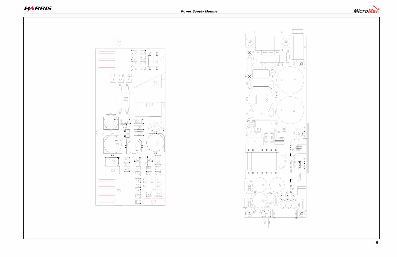
Power Supply Module
16
DZ4
1N4148
R15
3K9
R18
5K49
2
13
Q4
2N5064
1 2
C3
XX
R12
1K
R8
XX
12C4
CP.22KuF
Q2
BC237
12
C11
CD1K5PF-5%
R1310K
12
C6CD330pF-X7R
12
C8
CD.1uF
COMP1
V/FB2
ISENS3
RT/CT4
VREF8
VCC7
OUT6
GND5
U1
UC3843AD1-SO8
D3
BYM13-40
+C7
CE10/25
R3
5K6
R9
50R
R10
470K
R6
100R
1 2
C2
CD.1UF
12
C9CD.1uF
21
8
3 6 7
DZ3TL431CDSO8
12
C12
CD.1uF-X7RR14
47K5
R1920K
R7
2K47
12C10
CD3K3-5%-NPO
12
43
IS1
K10102A
R1
22R
R16
X22R
1 3
2
TR2
10K
D1
BAS83
13
2
TR1X50K
I_SENS
+C16
CE22/25
R21
22K
12
C17
CD.1uF X7R
VOUT=2495*(1+R5/R4)
1
3 2
Q1NDS352AP
+C19
CE2.2/25
R20 100K
D2
1N4148
1 2 3
JP2
STRIP-M90-6mm
DZ15V1-0.5W
GND_E EN
1234
JP1
STRIP-M90-6mm
OUT_G
VDD
DZ2
15V-1W
Q3
X2N7002
GND
+C18
CE100/25
VR
GND
R4
22R
1 2
C1
CD.1uF-X7R
1 2
C13
CD.33uF-X7R
R17
10K
12
C15CD1KPF-X7R
1 2C14
CD0.1uF-X7R
12
C5CD10KpF-X7R
R1156K
R51K
R2
560R
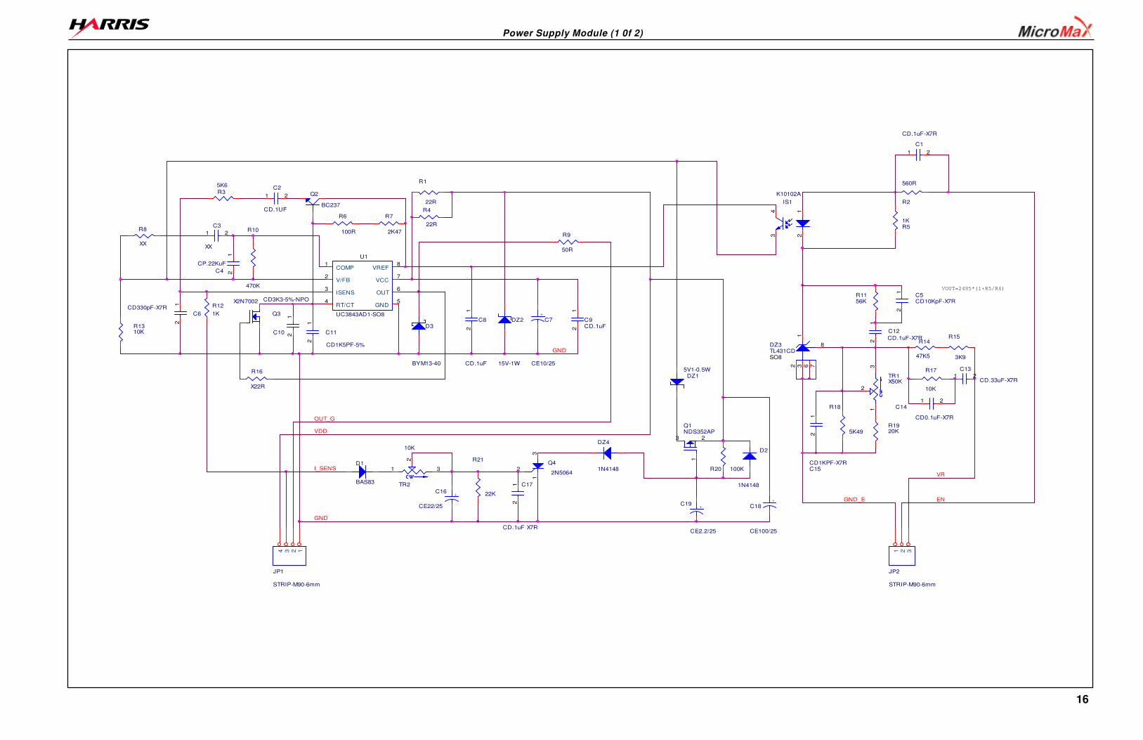
Power Supply Module (1 0f 2)
17
FAN
+BAT
24VDC
5VDC
1234
JP4
STRIP4-F
1 2 3
JP5
STRIF3-F
GND_AC
18VDC
18VDC
5VDC
+ C1CE47/35
R1 1M-1W
R4
100K/2W
F4VK200
D7
ISL9R460P2
+
C24
47/35
+
C21
100/4
00
+
C22
100/4
00
-+
BR1KBL06
12
C28XCD1KPF-1KV1
2
JP3
2.5MSF
1 2 C27 0.1uF-X2
STDBY
PE
1
FIX2FIX35
PE
1FIX4FIX35
1FIX3FIX35
RV1
10N431K
1
FIX1FIX35
13
2
f
F6 BL02
DZ3
P6KE200
1 2C15
XCD2K2pF-Y2
12
C3
CP
.1uF
/400
D1UF4006
D5
XU1550
RT1NTC10R
1 2 C2 0.1uF-X2
1
32
D6
BYQ28E
R5100R
R7X10R/2W
D4
UF4006
R8
100K/2W
12
C11
CD100PF-1KV
+
C102200/35
+
C6
2200/35
+
C5
2200/35
1 2 C17
CD2K2pF-Y2
1 2 C16 CD2K2pF-Y2
FS13101-0050f use 90gr
DZ415V-1W
12
JP2
2.5MSF
R161K
R152K2
DL7
LEDV-3D
DL6
LEDV-3D
D3UF4006
DZ1P6KE200
6
1
8 1615
1413
2
4
7
9101112
T1
TSWTCH6
R21OK-A.F.
R3 4R7-A.F.1
23
Q111N60C
R10
0.68R/2W
13579111315
2468
10121416
J2
FLAT-16A
12
C23
CD10KPF-1KV
R9
0.68R/2W
12
C13
CD
10K
pF
-1kV
+ C2647/35
13
2
f
F2 BL02
+ C2547/35
VI1
GN
D2
VO3
U3LM7818
D2P600G
1 2
3 4
F5CVO.1A8.10M-E2x10mH 1.8A
1 2 3
JP1
KP01-1112-11
13
2
f
F1 BL02
13
2
f
F3 BL02
+
C9
100/4
00
12
C8CD.1uF
12
C4CD4K7pF
J1FAST-ON
VI1
GN
D2
VO3
U1LM7805
R6
RUE300
R11
RUE300
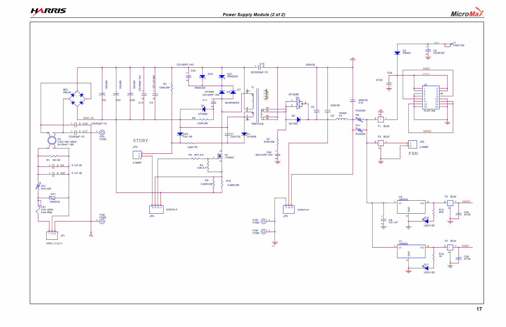
Power Supply Module (2 of 2)
18
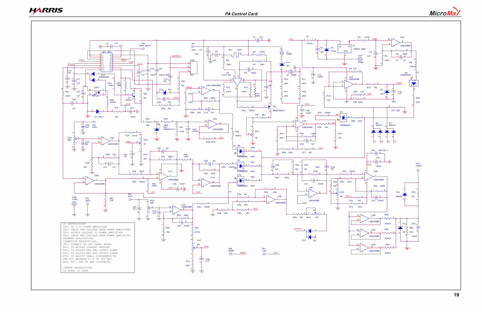
PA Control Card
19
1 23 45 67 89 1011 1213 1415 16
JP1 NC
12
R77 1M0
12
R87
NC
12
R19
10K0
12
+ C8
220uF/35V
12
R73
4K7
CNTFLY
VS
1
GND
3
V0
2
U7
LM50C_SMD
1
23
Q1BC847
EAGC
-VCC
FWD
1 2
R1
470H0
1
23
D9
HSMS2800
1
23
D5
HSMS2800
FIX1
FIX35
1
23
D10
HSMS2800
1
34
6OPT1
TLP181
21
D16
BAS32
12
C3
1uF
12
R52 10K0
TP8TEMP
1 2R49 100H0
TEMP
1 2
R43 100H0
1 2
R53 20K0
12
C451nF
13
2
cw
RV7
5K
VCC
12
R76
NC
1 2
C36 470nF
1 2
C19 1nF
RFD
5
67
+
-
U1B
LM324SMD
1 2
R30 1K0
ICC
3
21
411
+
-
U1A
LM324SMD
12
1314
+
-
U2D
LM324SMD
12
C421nF
12
1314
+
-
U1D
LM324SMD
FIX2FIX35
1 2
R37 51H0
ICC12C2 1nF
1 2
R68 NC
12
C43NC
10
98
+
-
U1CLM324SMD
21
D1
Z10V
RFD
EAGC
XI
1 2
R64 0H0
FWD
1 2
R71 NC
1
2
3
CN2
NC
1 2
R78 NC1 2
R79 0H0
12
C17
1nF
1 2
R60
220H0
1 2
R65
220H0
1 2R69
220H0
FOLD
12
R5
9K31
1 2
R3 20K0
TP5GND
12
R8
100H0
1 2
C7 1nF
12
3
D3HSMS2800
12
C4
4n7
1 2
C23 1nF
12
R32
100H0
TEMP
1 2
R26 1K0
TP2FWD
12
C11
1nF
TP4RFD
TP3CONT.
12
C6
1nF
TP1
VPA
XT
21D15 NC
12
R57
NC
12
C441nF
12
R85
NC
1 2R2 51H0
12
R66
1K8
1 2R62 24K3
21
D4
Z5V1
TEMP
1 2+
C20 NC
12
C35
100nF
10
98
+
-
U2C
LM324SMD
5
67
+
-
U2B
LM324SMD
13
2
D6BAV70
13
2
D7BAV70
12
R39
1K0
3
21
411
+
-
U2ALM324SMD
-VCC
12R38 1K0
10
98
+
-
U3C
LM324SMD5
67
+
- U3B
LM324SMD
3
21
411
+
-
U3A
LM324SMD
1 2R54 NC
12
1314
+
-
U3D LM324SMD
12
R58 0H0
1 2
R55 0H0
1 2
R59 NC
1
23
D8
HSMS2800
3
21
411
+
-
U4A
LM324SMD
5
67
+
-
U4B
LM324SMD
12
1314
+
-
U4D
LM324SMD
10
98
+
-
U4C
LM324SMD
1 2
C46 100nF
12C13
NC
12
C401nF
XI
12
R21
10K0
XR XE XT
CNTFLY
1 2
C21
100nF
XE
1 2R20 1K0
1 2
R22 10K0
1 2C1 4n7
1 2R28
1K0
JUMPER DESCRIPTION:
J2 OPEN, J1 OPEN
1 2
R56 100H0
1 2R29
18K0
12
R31
11K5
12
C22470nF
+3.9
21
D11
NC
12
R88 0H0
VCC
SH1 0H01
12
R611K0
12
R700H0
13
2
cw
RV220K
13
2
cw
RV320K
1 2
R80
0H0
+3.9
1 2
R82
0H0
2 1
D17 Z5V1
1 2
R81
0H0
12
R6
10K0
1 2
R25 100H0
TP DESCRIPTION:
TP1: PA V TO POWER AMPLIFIER
TP2: INPUT FWD VOLTAGE FROM POWER AMPLIFIER
TP3: OUTPUT VOLTAGE TO POWER AMPLIFIER
TP4: INPUT RFD VOLTAGE FROM POWER AMPLIFIER
TRIMMER DESCRIPTION
CONNECTOR DESCRIPTION:
JP1: CONNECT TO CPU PANEL BOARD
RV1: TO ADJUST CURRENT READING
RV2: TO ADJUST MAX FWD OUTPUT POWER
RV3: TO ADJUST MAX RFD OUTPUT POWER
RV5: TO ADJUST SMALL DIFFERENCE OF
PWR OUT BETWEEN 87.5 TO 108 MHz
RV6, RV7: SET AT MAX CLOCKWISE
1 2R27 4K7
12
R34
5K61 2
R36 10K0
21 3
DZ1LM4040-10 V
12
C27 1nF
VCC
1 3
2
cw
RV4 NC
1 2R40 10K0
1 2R9 NC
1 2
R12 1K0
3 26
71
45
-+
U5TL071/SO
1 2R41 20K0
12C25 NC
VCC
12
R5120K0
1 2
R50 100H0
12
C161nF
12
R7 10K0
FOLD
12R4 51H0
1 2
R63 NC
+3.9 XR
12
R33
1K0
12
R75
1K0
+3.9
12C28 NC
12
R67
51H0
12
R86
1K8
1 2R74 100H0
12
J1JSMD
-VCC
12
R2310K0
13
2
D13 NC
TP6PWR_INPUT
VCC
TP7+18V
12
R10
0H0
12
R17
0H0
VCC
12
R18
0H0
1 2
R46 10K0
12
R11
0H0
1 2
R83 0H0
12
R84
0H0
12
C141nF
12
R89220H0
1 2R24 20K0
1 2
C34
1uF
1 2
C32
100nF
12
R14
47K0
12
+
C15
NC
12
R13
47K0
12
C5
4n7
12
R1510K0
12
C18
1nF
1 2
R4210K0
13
2
cw
RV5
5K
VCC
12
J2 JSMD
1 2
C9 100pF
13
2
cw
RV6
1K1
2
C10
100nF
1
23
Q2
MMBT540LT1
1 2
R35 51H0
+3.9
12
R72
6K8
1 2
R48
47K0
12
R45
NC
1 2
R47 10K0
12
R44
NC
12
C30NC
12
C29
NC
1 2
C31 470nF
12
C26
100nF
13
2
D12HSMS2804
1 2+
C41 10uF/35 V
1 2
C33 470nF
12
C241nF
21
D14
NC
13
2
cw
RV1
5K
12
C12100nF
12
R16
1K0
PA Control Card
20
Power Amplifier Module
21
2
41 3
Q4BFG35
L7NC
L1147nH
12R57 1k5
12
R7710R
12 R78
10R1 2
C70 NC
2 1
D11 9V1
1 2
C58 470p
1 2
C55 470p
12
+
C39 10uF
12
R834R7
12
R7551R
12
R48180R
12
R47180R
12
C31470p
2
41 3
Q1BFG35
12
R49180R
12
R50180R
12
C32470p
12R30 2R2
12
R33 2R2
12R40 4R7
TL1
TLTL2
TL
12R59 4k7
TL4 TL
1 2
C5627p
1 2
3
D12HSMP3810
12
C38NC
12
R89100R
12
R45220R
12
C68NC
12R65 NC
12
R74NC
TL9
TL
1 2R35 51R1W
1 2R34 51R1W
12R61 51R
12R67 180R
12R66 51R
12
+
C37 10uF
1 2
R9022R
L15175nH
1 2
C784p7
12
+
C1810uF
L10 2uH2
TL8 TL
12
R7351R1W
12
R7651R1W
12
C12NC
12
C44NC
12
C71470p
12C51 470p
21
D49V1
12
R181k5
21
D39V1
TL7
TL
L875nH
12
C6022p
12
C6168p
12
C6256p
CPT41n
W4WIRE
BIAS 1 2
R922R
12
R54270R
1 2R16 22R1W
1 2R17 51R1W
12
J1 JSMD
1 2R15 51R1W
1 2R14 22R1W
1 2R13 51R1W
L968nH
1 2C48 68p
1 2C42 22p
1 2R51 NC
L585nH
1 2R53 NC
L235nH
1 2R23 51R1W
1 2R20 22R1W
1 2R19 51R1W
1 2R21 51R1W
1 2R22 22R1W
1 2R27 51R1W
1 2R28 22R1W
1 2R29 51R1W
1 2R25 51R1W
1 2R26 22R1W
12
C34470p
12
C23NC
12
C2222p
1 2R36 51R1W
1 2R37 22R1W
L4VK200
12
R3922R1W
12
R72 100R
1 2C45 4n7
12
C26470p
12
+
C25100uF 35V
12
C11100n
L62uH2
12
C97_50p
1 3
2
cw
RV1 1k
12J2
JSMD
12
R521k
1 2C29 4n7
1
23
4
765
DCPLR1DIR_CPLR
12
C63100p
1 2
C57 150p
PD1PAD
12
C64100p
12
C65NC
12
R651R1W
12
R111k
12
R751R1W
12
C8NC
12
C131p
12
C67NC
12
C66NC
12
C54n7
1 2C77 100n
L12 NC
12
C27100n50V
12
C14n7
12
R547
12
C24n7
12
R847
1 2
3
D2HSMS2800
1 2
3
D1HSMS2800
12
C34n7
12
R8822R
12
C44n7
W7WIRE
12
C64n7
1
2
CN3BNC_P
1
2
CN2BNC_P
12
C151p
12
C2147p
12
R2456
L395nH
12
C724n7
1 2C33 68p
1
2
CN1BNC_P
12
C694n7
1 2C16 NC
12C40 100n
12C49 4n7
12
R4351R1W
12 C20
4n7
12
R110k
12
R210k
12
R4 1k
12
R3 1k
L14 NC
L118nH
12 C74
NC
12 C73
NC
12R81 22R
TL3TL
12R60 390R
12 C19
100n
12R56 390R
CPT21n
CPT11n
W2WIRE
W1WIRE
12
C304n7
1 2C50 4n7
21
D5SM4004
12
C36100n50V
12
C354n7-50V
FWD
REF
21
D6SM4004
21
D7SM4004
21
D9SM4004
21
D8SM4004
21
D10SM4004
12
C104n7
1 2
C41470p
12
C47470p
COAX1
RG316
12
C7
4n7-50V
12
R622R21W
COAX2
NC
32
1
4
MOS1BLF245
12
R3822R1W
12
C54NC
12
R632R21W
12
+
C1710uF
12
R4651R
12
R85180R
2
41 3
Q3BFG35
12
R10180R
1 2
R42 270R
12
R44270R
12
C75470p
12
R12180R
12
R84180R
W3WIRECPT3
1n
SUPPLY
12
C76470p
12
R86180R
12
R87180R
12
C46470p
12R82 4R7
12R79 2R2
12
R80 2R2
1 2C14 NC
1 2C28 NC
1 2
C5927p
1 2
C24 NC
TL11
TL
TL10
TL
1 2
C43 NC
1 2
R31 270R
1 2
R32 270R
1 2
R41 270R
12
C52470p
12
R69180R
12
R70180R
12
R71180R
12
C53470p
12
R68180R
12R55 2R2
12
R58 2R2
12R64 4R7
24
1 3
Q2BFG35
TL5
TLTL6
TL
L1325nH
Power Amplifier Module
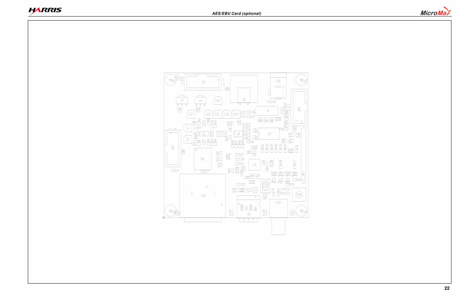
22
AES/EBU Card (optional)
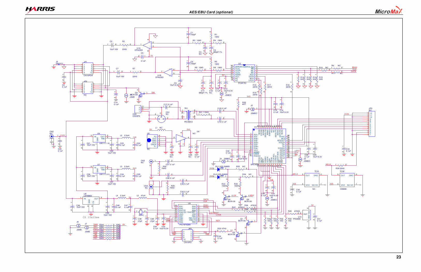
23
CN4NC
5V
13
2Q2
BCR135
1 2C17 0.1uF
1 2R21 110H0
12
C240.1uF
123456789101112
JP3NC1 2
C18 0.1uF
1 2
C19 0.1uF
1 2
R2
22H0
12
R2275H0
12
C460.1uF
LCK
1
32
Q3BCR135
SW
12
R331K0
1V8
12
+ C4410uF/16V
12
+
C4510uF/16V
ZEROL/NA1
MS2
MC3
MD4
SCK5
DATA6
BCK7
LRCK8
NC9 NC
10 VCC11 AGND12 Vcom13 VoutR14 VoutL15 ZEROR/A16
U2
PCM1781
12
R1822H0
1 2
C39 0.1uF
1 2C43 0.1uF
5V
1 2
R7
22H0
L1 NC
12
34 5
6
78
TR1
PE-65812
1 2R29 470H0
TXD
IN3
OUT2
TAB4
GN
D1
U4
LM1117-1.8
12
+
C1310uF/6.3V
12
C120.1uF
IN3
OUT2
TAB4
GN
D1
U7
LM1117-3.3
12
J1
JSMDC
12
+ C2110uF/16V
RA21
RA32
RA43
RA5/MCL4
VSS5
RB06
RB1/RX7
RB2/TX8
RB39
RB410 RB511 RB612 RB713 VDD14 RA6/QO15 RA7/QI16 RA017 RA118
U9
PIC16F628A
1
32
Q4BCR135
LCK
12
+
C2210uF/16V
12
+ C3610uF/16V
12
+
C3710uF/16V
12
C520.1uF
12
C350.1uF
3V3
1 2X1
4MHz
RXD1 2R40 10K01 2R41 10K0
1 2R6 NC
TXDRXD
12
C49
27pF
1 2R34 10K0
1 2R10 NC
1 2R11 NC
12
C470.1uF
5V
5V
RX1+1
RX1-2
RX2+3
RX2-4
RX3+5
RX3-6
RX4+7
RX4-8
VCC9
AGND10
LOCK11
RXCKO12
RX
CK
I13
MU
TE
14
RD
Y15
DG
ND
116
VD
D18
17
CP
M18
CS
/A0
19
CC
LK
/SC
L20
CD
IN/A
121
CD
OU
T/S
DA
22
INT
23
RS
T24
MCLK25GPO126GPO227GPO328GPO429DGND230TX-31TX+32VDD3333AESOUT34BLS35SYNC36
BC
KA
37
LR
CK
A38
SD
INA
39
SD
OU
TA
40
NC
41
VIO
42
DG
ND
343
BG
ND
44
SD
OU
TB
45
SD
INB
46
LR
CK
B47
BC
KB
48
U3
SRC4382
2 4
53 1
U6NC
12R35 47H0
1 23 45 67 89 10
JP2
NC J8
JSMD
12 C4
680pF/1%
1 23 45 67 89 10
JP1
CN10PDA
12
C3NC
12
C340.1uF
12
C500.1uF
1
32
Q5BCR135
LED2
1
2
CN3NC
12
R204H7
DATAOUT
1 2J4 JSMDC
ENA2
12
R45150H0 NC/VC
1
GND2
OUT3
VCC4
TCX2
12M288
12
+
C3310uF/6.3V
12
C48
27pF
IN1
GN
D2
FX
4
OUT3
U8LM78M05
1 2R36 10K0
CLK
12
C320.1uF
DATA
MCLK
1 2R37 10K0
V12V
NC/VC1
GND2
OUT3
VCC4
TCX1
NC
1 2R38 10K0
1
32
Q1BCR135
J9GNDCC
1
2 3
CN2NC
12
C26NC
12
C300.1uF
5V
12
+
C2910uF/6.3V
12
C280.1uF
12
R1
15K0
1 2
C38 0.1uF
12
C230.1uF
ENA2
12
J3
JSMDC
5V
12
C270.1uF
1 2
C31 0.1uF
ENA1
3V3
12
C80.1uF
12
C420.1uF
MCLK
SW0
L5 47uH
1 2R4 15K0
12
R321K0
12
R311K0
12
R301K0
3V3
12
+
C1610uF/6.3V
12
C150.1uF
3
21
48
+
-
U1AOPA2353
12
J2
JSMDC
CLK
SW1
1 2R8 12K0
L2 2.2uH
3V3
3V3
RDY
1 2R42 10K01 2R43 10K0RB7
RB6
2 1DL1 LED-G0805
1 2R9 15K0
5
67
+
-
U1BOPA2353
LOCK
LED2
12
R1622H0
DATA
12345678910
JP4
CN10PD
SW1
2 1DL2 LED-G0805
1 2R3 12K0
3
1 2
4CN1NC
1 2R24 NC
3V3
12
+
C4110uF/6.3V
12
C400.1uF
12
R44150H0
1V8
1 2
R39 22H0
SW0
12
C11680pF/1%
12
J5
JSMDC
1 2+
C2
10uF/16V
LOCK
12
R5
15K0
GN
D1
RST2 V
dd
3
U10TPS3809
12
C140.1uF
12
C200.1uF
12
C10NC
12
+
C910uF/6.3V
12
C6150pF
OUT1
GND2
VCC3
GNDA4
F15
F26
U5
NC
12
R1722H0
RB6
12
R2575H0
L3 2.2uH
RDYJ6
JSMD
12
R150H0
1 2R23 NC
L4 2.2uH
12
R140H0
12
C1150pF
RB7
J7
JSMD
12 C51
0.1uF
V12V
112233
CN5CN03PS
12
C25NC
12
R1922H0
1 2R26 470H0
1 2R27 470H0
1 2+
C7
10uF/16V
1 2R28 470H0
12
R130H0
CS 15x15mm
12
R120H0
12
C5
0.1uF
12
+
C5310uF/6.3V
5V
3V3
SW
AES/EBU Card (optional)