Embed Size (px)
Citation preview

Micron scale deformation: a coupled in-situ study of deformation strain burst
and acoustic emission
Adam Istvan Hegyi,∗ Peter Dusan Ispanovity, Zoltan Dankhazi, Gabor Varga, and Istvan Groma
Department of Materials Physics, Eotvos University Budapest, H-1517 Budapest POB 32, Hungary
Michal Knapek, Krisztian Mathis, and Frantisek Chmelik
Charles University in Prague, Faculty of Mathematics and Physics
Department of Physics of Materials, Ke Karlovu 5 121 16 Prague 2
(Dated: March 29, 2016)
Plastic deformation properties of micron scale crystalline materials differs considerable
from the bulk ones. It is characterized by random stress or stain burst. To obtain a detailed
picture about this stochastic nature, micron sized micro-pillars have been fabricated and
compressed in the chamber of a SEM. An improved FIB fabrication method is applied to get
non-tapered precise shaped micro-pillars. The in-situ compression device developed allows
high accuracy of sample positioning and fast data sampling. The collective avalanche like
motion of dislocations appears as stress drops on the stress-strain curve. To confirm that the
stress drops are directly related to dislocation avalanches, not from some other effects, an
acoustic emission transducer has been mounted under the sample to record acoustic signal.
Stain controlled compression tests have been performed on Al 5% Mg micro-pillars. The
correlation between the stress drops and the acoustic emission signals indicated that indeed
dislocation avalanches are responsible for the stochastic character of the deformation process.
PACS numbers: 64.70.Pf, 61.20.Lc, 81.05.Kf, 61.72.Bb
I. INTRODUCTION
During the past decades miniaturizing mechanical and electronic devices inspired research on
determining the mechanical properties of micron sized specimens1–5. The vast majority of micro-
electromechanical sensors contain micrometer size pieces, e.g.: accelerometer measures the buckling
of a micro-cantilever or chemical and biological sensors use cantilever transducers as a platform6,7.
In order to be able to design devices that are even smaller, the detailed physical properties of the
deformation processes should be studied.
The plastic deformation of crystalline material is caused by the evolution of the dislocations.
In macroscopic samples, due to the large number of dislocations, the stress-strain response of the
material is smooth allowing to predict the properties of the material with a high accuracy. In

2
contrast to this, in micrometer scale the inhomogeneity of the dislocation microstructure is in
the order of the sample size resulting non-deterministic response due to the stochastic motion of
dislocations8–12. So, in order to design new microscopic devices the mechanical properties of a
micron size piece of material has to be described by a statistical approach.
The first evidence of intermittent crystal plasticity was obtained on ice single crystals by detect-
ing strong acoustic emission signal during plastic deformation13,14. A decade ago by compressing
pure single crystalline Ni micro-pillars Dimiduk et. al. found that instabilities, resulting strain
jumps, dominate the micrometer scale crystal plasticity15–17 raising the questions, what is the
limit between microscopic and macroscopic deformation, and how one can define material strength
parameters, like flow stress, for micron scaled objects18,19.
Due to its statistical nature to determine the properties of micro-deformation a vast amount
of micrometer size samples are needed. One of the easiest way to fabricate them is FIB milling20.
Several advantages and disadvantages of this method have been published, but one of the main
advantage is that one can visually check the result of ion patterning. To shorten the fabrication
time of the micro-pillars several different growing (FIB-less) methods are developed21,22. These,
however, do not allow to produce pillars from any type of material, and to vary the initial dislocation
contents in the samples. Moreover, for pillars produced by growing the connecting force between
the substrate and the micro-pillar itself can be rather weak.23.
To fabricate micro-pillars by FIB milling two approaches are commonly applied: “lathe” and
“top-down” millings24. Lathe-milling uses ion beam perpendicular to the axis of the micro-pillar’,
and the pillar is rotated around to get the cylindrical shape. Usually this procedure is used on the
side of a thin layer of a crystal material. In the top-down technique the pillar axis is parallel to the
ion beam, the ions etch the surface of the sample prepared. In this case, however, the height of the
micro-pillar and its tapering are poorly controlled. The new method outlined below combines the
advantages of both fabrication techniques. With this procedure a non-tapered micro-pillar can be
obtained anywhere on the surface of a bulk material, and much less preparation time is required25.
Moreover, by this technique it is possible to investigate in-used parts in a quasi non-degradable
way.
In the studies presented our main goal was to get an insight into the fundamentals of plastic
deformation in micrometer scale. The new fast micro-pillar fabrication procedure developed gives
us the chance to perform a statistical analysis of the deformation processes. This is essential
because during an individual compression experiment the stress varies intermittently (see below),
meaning that the dislocation system give stochastic response to the acting force11,14,26,27. As a
3
result of this defining material parameters from a unique measurement is impossible. So, hardness,
or strain hardening can only be calculated from a statistical analysis28.
The compression tests were performed on Al 5% Mg alloy micro-pillars fabricated onto the
surface of a bulk material. The unique feature of this allow is that it shows the Portevin-Le
Chatelier (PLC) effect29–32 too. So, even for bulk samples intermittent stress-strain response is
observed which is related to the pile-up and break out of the dislocations from the solute atom
atmosphere acting as junctions for mobile dislocations31,32. This mechanism also generates acoustic
emission signal with energy that is slightly higher than the one caused by dislocation avalanches.
Since the stress drops caused by PLC and dislocation avalanches are clearly distinguishable the
tests on this material allowed us to determine the sensitivity of our acoustic emission detector
setup.
II. SAMPLE PREPARATION
Before the actual pillar fabrication the size of the micro-pillar has to be selected. Since in this
study we are interested in the collective dislocation motion, we have to have enough dislocations
in the system initially. On the same time the sample size should not be too large to hinder the
stress drops. Normally in fcc metals like Al the dislocation density varies between 1011− 1014m−2.
Therefore the average spacing between dislocations is about 3−0.1µm. Since the dislocations tend
to form a cell like structure with a characteristic size of about 10 time the dislocation spacing, the
pillar size should be selected in the order of the cell size to get statistically relevant results.
In-situ micro-pillar deformation test demand very careful and particular sample preparation.
To get the necessary surface properties, orientation, and initial dislocation density the following
steps were performed: after a short etching the Al 5% Mg sample was electropolished in struers
D2 solution with 60 mAmm2 current density. The lattice orientation was measured using electron back-
scattered diffraction (EBSD). The sample was cut by an electric discharge machining (EDM) to have
a surface orientation 〈1, 2, 3〉. After this, another electropolishing step was made, then the sample
was heat treated for 72 hours at 200C0. After the heat treatment, the surface was electropolished
again with 30 mAmm2 and the orientation was checked again by EBSD. The sample was pre-deformed
parallel to the 〈1, 2, 3〉 axis to 20MPa. The initial dislocation density was measure by TEM and
X-ray line profile analysis. It was found to be 2× 10¹³m−2. Taking this value into account, pillars
with rectangular cross section of 4 × 4µm2 was selected with high of 12µm corresponding to a
aspect ratio 3 commonly applied in earlier studies.
4
FIG. 1: A) The initial FIB milling step marked by the grid to fabricate the “raw ” pillar and the hole
around it necessary to carry out the compression test. At this milling step 30nA ion current is applied. B)
The second finalizing milling step with 45◦ ion direction angle (see Fig. 2 too). The area removed by this
step is marked by the grid. The ion current is 5nA. Both pictures are taken from the ion direction.
FIG. 2: The details of the second finalizing step of the micro-pillar fabrication process with ion current
5nA A) After the first step seen on Fig. 1 the sample is rotated by 45◦ resulting a tilted ion beam direction.
After this, two rectangular FIB patterns (marked by the red grid) are used to get the surface marked by red.
B) As a next step the sample is rotated by 180◦, and two rectangular FIB patterns are used again to get the
surface marked by yellow. With a rotation by 90◦, and repeating the two previous steps the surfaces marked
by green (C) and blue (D) are obtained. With these a square shaped pillar is achieved. In order to get a
pillar with smooth surface and minimal tapering the process is repeated with ion currents 1nA, and 100pA
too. The pillar obtained is seen in the inset.
After the above mentioned sample preparing processes a “surrounding hole” is milled by 30nA
ion current around the pillar. The FIB milling pattern used is marked by the grid in Fig. 1/a. The
5
sample was oriented so that the normal vector of the surface was parallel to ion beam direction.
Then a thin Pt layer is deposited onto the top surface of the micro-pillar. The cap helps the ion
beam to fabricate smooth side surface of the pillar and due to its amorphous structure it is very
hard which can help to eliminate effects related to the missalignment of the compressing head (see
below). To do the next step the stage is tilted by 7◦. Due to the 52◦ ion-electron beam angle
this result in a 45◦ ion beam direction compared to the surface normal. To avoid irregular sample
motions related to the random drift of the microscope stage a 2µm size cross was drawn to the
geometric center of the top surface of the micro-pillar. After this the milling steps explained in the
caption of Fig. 2 were performed. In order to further decrease tapering33 a final “polishing like”
step is performed with 30pA ion beam over-tilted by 1◦ compared to the pillar axis.
Apart from the first step explained above the fabrication works with high surface angle. This
increases the effectiveness of the milling by a factor of 2,5-3 compare to the perpendicular beam
setup commonly used34. The 45◦ milling direction applied in the second phase lets us to fabricate
micro-pillars anywhere on the sample chosen previously.
It has to be mentioned, that the Ga ion beam forms an irradiated skin onto the micro-pillar.
The slightly tilted final “polishing” step with the reduced 10pA ion current and the (20kV or10kV )
lowered acceleration voltage decrease the thickness of this layer resulting a negligible effect at the
size of the pillar used35.
To sum up the most important advantages of the milling procedure proposed are: pillars can
be fabricated at any position of the surface, and the preparation is touchless so the damage or the
deformation of the pillar can be avoided, effect related to tapering and Ga implantation can more or
less be eliminated too. It should be noted that in spite of our efforts to automatize the procedure,
due to the slow drift of the sample, have not been successful. The built in drift compensation of
the AutoFIB software is not accurate enough to get well shaped micro-pillars.
III. IN-SITU DEVICE
An in-situ micro-mechanical test requires that the testing device is place inside the chamber of
the microscope. We have developed a compression device suitable to place inside the chamber of a
FEI Quanta 3D scanning electron microscopes. The sketch of the device is shown in Fig. 3.
Two linear ultrasonic motors are used for the X and Y positioning of the sample (see Fig. 3).
The AE transducer is mounted onto the two stages. In Z direction two stages are used. One is a
linear step-motor stage used for the ”raw“ motion of the compressing tip to get it close enough to

6
FIG. 3: Sketch of the in-situ device NANOTEST.
the sample. The other one mounted on the linear step-motor stage is a piezoelectric positioning
(PEP) stage with about 0.1nm resolution. During the actual compression test only this stage is
moved. To measure the external force a standard spring mounted on the PEP stage is used with
strong transverse but very weak longitudinal stiffness. The displacement of the spring is measured
by a capacitive sensor with 0.1nm resolution. If the PEP stage is moved by the distance P , and
the force sensor having S spring stiffness measure the force F acting on the pillar the sample
deformation is D = P − F/S. The pillar compression is performed by a flattened diamond tip. It
should be mentioned that to avoid the charging of the compressing head in the SEM a tip doped
by boron has to be used.
For being able to measure instabilities related to PLC effect and dislocation avalanches it is
crucial to have a fast enough feedback controlling system and minimum of 1kHz data collection
rate. These are achieved by an analogous PID type feedback electronics and a fast 16bit AD
converter.
The range and the resolution parameters of the device are summarized in Table 1.
TABLE I: Parameters of the nanodeformation device
Part name Total range Resolution Accuracy
X and Y ±8µm 0.5µm 0.01µm
Z coarse 9mm 2µm 0.5µm
Z fine 35µm 1nm 0.1nm
Force sensor 20/50mN 1/2.5µN 1/2.5µN
To meet these resolutions the thermal and elastic elongation of the different parts have to be
negligible during the typically few minutes of the measuring time. In order to achieve this, several
different additional part are added to the compression device. One main problem is to reduce the
heat produced by the motors of the stages. The Quanta 3D has an environmental stage with a
7
Peltier sample holder to set the sample temperature. The cold point of this Peltier stage is mounted
to the bottom of the device. By this, the temperature is stabilized at 15◦C. Another important
issue is to eliminate the noise generated by the different vibrating parts of the microscope. Due
to the lack of air the spring in the force sensor is not damped. To avoid this rather disturbing
effects a strong permanent magnets are placed close to the lamellas of the force measuring spring
resulting the necessary damping due to the eddy current.
IV. ACOUSTIC EMISSION MEASUREMENT
An Acoustic Emission (AE) measuring system was also employed to study the dynamic processes
appearing during the plastic deformation of micropillars. Acoustic emissions are transient elastic
waves generated by the rapid release of energy from localized sources within the material. Thus, AE
signal is generated at the sudden localized structural changes, like dislocation motion or twinning.
So it provides information on the dynamic processes involved in plastic deformation36.
In bulk materials, a direct correlation of AE parameters with the stress-strain curves can reveal
the activation of different deformation mechanisms37–39. It is important to noted that the collective
motion (at least several tens or hundreds) of dislocations is necessary in order to obtain a detectable
AE signal40. So, in terms of AE, a motion of single dislocation is typically ”silent“ and, in turn, a
detectable AE signal reflects the cooperative character of dislocation motion.
At micro-scales, the ”crackling“ or avalanche-like type of plasticity39 is observed. Thus, the AE
technique, have a great potential to provide information on the dynamic processes behind the step-
like nature of deformation curves recorded during the micro-pillar testing. Up to the knowledge of
the authors, the study presented in the paper is the first attempt to record the AE signal during
the micro-pillar compression.
The acoustic emission (AE) signal measurement was performed by a Physical Acoustics PCI-2
acquisition board based on a continuous storage of AE signals with 2MHz sampling rate. The full
scale of the A/D converter was ±10V . The AE was amplified by 60dB in the frequency range of
100 − 1200kHz. The background noise during the tests did not exceed 24dB. Due to this small
noise level the detecting threshold level was set to 26dB. The AE was recorded simultaneously
during uni-axial compression of micro-pillars.
A rectangular piece of material (with pillar samples fabricated onto its surface) was attached
directly to the AE transducer using a metallic spring. In addition, the acoustic contact was
improved by means of a vacuum grease.
8
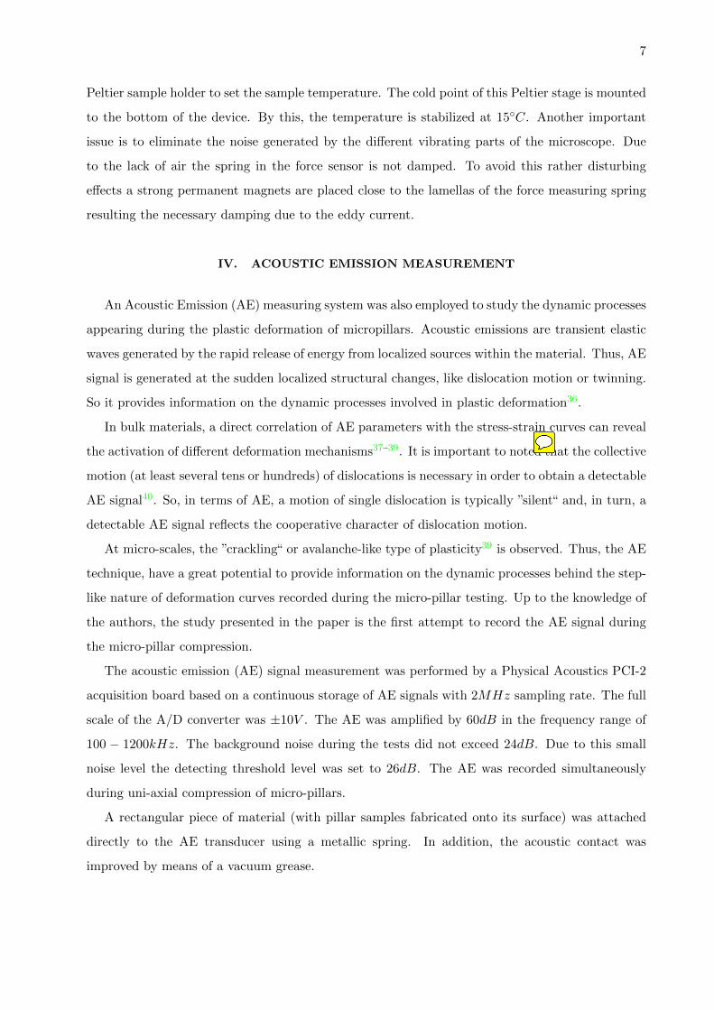
V. RESULTS
The load as a function of the time together with the acoustic emission signal obtained on a Al
5% Mg micro-pillar at a constant compression strain rate is plotted in Fig. 4. As it is expected the
sample show the well known PLC effect. The stress drops at the very begging of the deformation and
just before plastic yielding (enlarged in inset a)) can be attributed to the breakout of dislocations
from the surrounding solute atoms. As it is seen in inset a) just at the onset of the stress drop a
large acoustic emission signal is detected.
At the micro-pillar size (4x4x12 µm3) used in the test the PLC effect competes with the in-
termittent dislocation motion related to the small system size (dislocation avalanches). This dual
effect destroy the well known periodic stress drop structure of the deformation curve, and ran-
domly distributed avalanches can be found. In inset b) the waveform of the acoustic signal can be
seen. The large peaks on the acoustic emission signal are generated by collective motion of many
dislocations.
FIG. 4: Load versus time curve obtained by a micro-pillar compression with constant strain rate. In inset
a) a stress drop is enlarged. Inset b) shows the waveform of an acoustic signal.
VI. SUMMARY
In order to understand the detailed deformation properties of micron sized object many more
experiment are needed. The pillar fabrication method presented in the paper is faster considerably
9
than the ones applied earlier. This opens the possibility to carry out investigations that can reveal
the statistical properties of micron scale plasticity. The results obtained indicates that detecting
acoustic emission signal related to the cooperative motion of dislocations is feasible from the small
(about 100 µm2) volume corresponding to a micro-pillar is feasible.
Acknowledgments
Financial supports of the Hungarian Scientific Research Fund (OTKA) under contract numbers
K-105335 and PD-105256 and of the European Commission under grant agreement No. CIG-
321842 are also acknowledged. PDI is supported by the Janos Bolyai Scholarship of the Hungarian
Academy of Sciences.
∗ Electronic address: [email protected]
1 C. A. Volkert and E. T. Lilleodden, Philosophical Magazine 86, 5567 (2006).
2 K. Ng and A. Ngan, Acta Materialia 56, 1712 (2008).
3 C. Zhou, I. J. Beyerlein, and R. LeSar, Acta Materialia 59, 7673 (2011).
4 M. Zaiser, J. Schwerdtfeger, A. Schneider, C. Frick, B. G. Clark, P. Gruber, and E. Arzt, Philosophical
Magazine 88, 3861 (2008).
5 O. Kraft, P. A. Gruber, R. Monig, and D. Weygand, Annual review of materials research 40, 293 (2010).
6 N. Yazdi, F. Ayazi, and K. Najafi, Proceedings of the IEEE 86, 1640 (1998).
7 N. V. Lavrik, M. J. Sepaniak, and P. G. Datskos, Review of scientific instruments 75, 2229 (2004).
8 J. Weiss and D. Marsan, Science 299, 89 (2003).
9 M. Zaiser, F. M. Grasset, V. Koutsos, and E. C. Aifantis, Physical review letters 93, 195507 (2004).
10 M. Zaiser and P. Moretti, Journal of Statistical Mechanics: Theory and Experiment 2005, P08004 (2005).
11 M.-C. Miguel, A. Vespignani, M. Zaiser, and S. Zapperi, Physical review letters 89, 165501 (2002).
12 S. Zapperi, The European Physical Journal B 85, 1 (2012).
13 J. Weiss, F. Lahaie, and J. R. Grasso, Journal of geophysical research-solid earth 105, 433 (2000).
14 M.-C. Miguel, A. Vespignani, S. Zapperi, J. Weiss, and J.-R. Grasso, Nature 410, 667 (2001).
15 M. D. Uchic, D. M. Dimiduk, J. N. Florando, and W. D. Nix, Science 305, 986 (2004).
16 D. M. Dimiduk, C. Woodward, R. LeSar, and M. D. Uchic, Science 312, 1188 (2006).
17 M. D. Uchic, P. A. Shade, and D. M. Dimiduk, Annual Review of Materials Research 39, 361 (2009).
18 E. Arzt, Acta materialia 46, 5611 (1998).
19 J. R. Greer and J. T. M. De Hosson, Progress in Materials Science 56, 654 (2011).
20 S. Reyntjens and R. Puers, Journal of Micromechanics and Microengineering 11, 287 (2001).
10
21 A. T. Jennings, M. J. Burek, and J. R. Greer, Physical review letters 104, 135503 (2010).
22 M. J. Burek and J. R. Greer, Nano letters 10, 69 (2009).
23 G. Moser, H. Felber, B. Rashkova, P. Imrich, C. Kirchlechner, W. Grosinger, C. Motz, G. Dehm, and
D. Kiener, Practical Metallography 49, 343 (2012).
24 J. Hutsch and E. T. Lilleodden, Scripta Materialia 77, 49 (2014).
25 S. Wurster, R. Treml, R. Fritz, M. Kapp, E. Langs, M. Alfreider, C. Ruhs, P. Imrich, G. Felber, and
D. Kiener, Practical Metallography 52, 131 (2015).
26 M. Zaiser, Advances in physics 55, 185 (2006).
27 P. D. Ispanovity, I. Groma, G. Gyorgyi, F. F. Csikor, and D. Weygand, Physical review letters 105,
085503 (2010).
28 P. D. Ispanovity, A. Hegyi, I. Groma, G. Gyorgyi, K. Ratter, and D. Weygand, Acta Materialia 61, 6234
(2013).
29 T. Tabata, H. Fujtta, and Y. Nakajima, Acta Metallurgica 28, 795 (1980).
30 N. Chinh, F. Csikor, Z. Kovacs, and J. Lendvai, Journal of Materials Research 15, 1037 (2000).
31 J. Gubicza, N. Q. Chinh, Z. Horita, and T. Langdon, Materials Science and Engineering: A 387, 55
(2004).
32 A. Yilmaz, Science and Technology of Advanced Materials (2016).
33 J. Li, T. Malis, and S. Dionne, Materials characterization 57, 64 (2006).
34 T. Ishitani, K. Umemura, T. Ohnishi, T. Yaguchi, and T. Kamino, Journal of electron microscopy 53,
443 (2004).
35 J. R. Greer, H. Espinosa, K. Ramesh, and E. Nadgorny, Applied Physics Letters 92, Art (2008).
36 C. Heiple and S. Carpenter, Journal of Nuclear Materials 149, 168 (1987).
37 J. Bohlen, F. Chmelık, P. Dobron, D. Letzig, P. Lukac, and K. Kainer, Journal of alloys and compounds
378, 214 (2004).
38 P. Dobron, F. Chmelık, J. Bohlen, K. Hantzsche, D. Letzig, and K. Ulrich Kainer, International Journal
of Materials Research 100, 888 (2009).
39 J. Weiss, T. Richeton, F. Louchet, F. Chmelik, P. Dobron, D. Entemeyer, M. Lebyodkin, T. Lebedkina,
C. Fressengeas, and R. J. McDonald, Physical Review B 76, 224110 (2007).
40 C. Scruby, H. Wadley, K. Rusbridge, and D. Stockham-Jones, Metal Science 15, 599 (1981).