Embed Size (px)
Citation preview
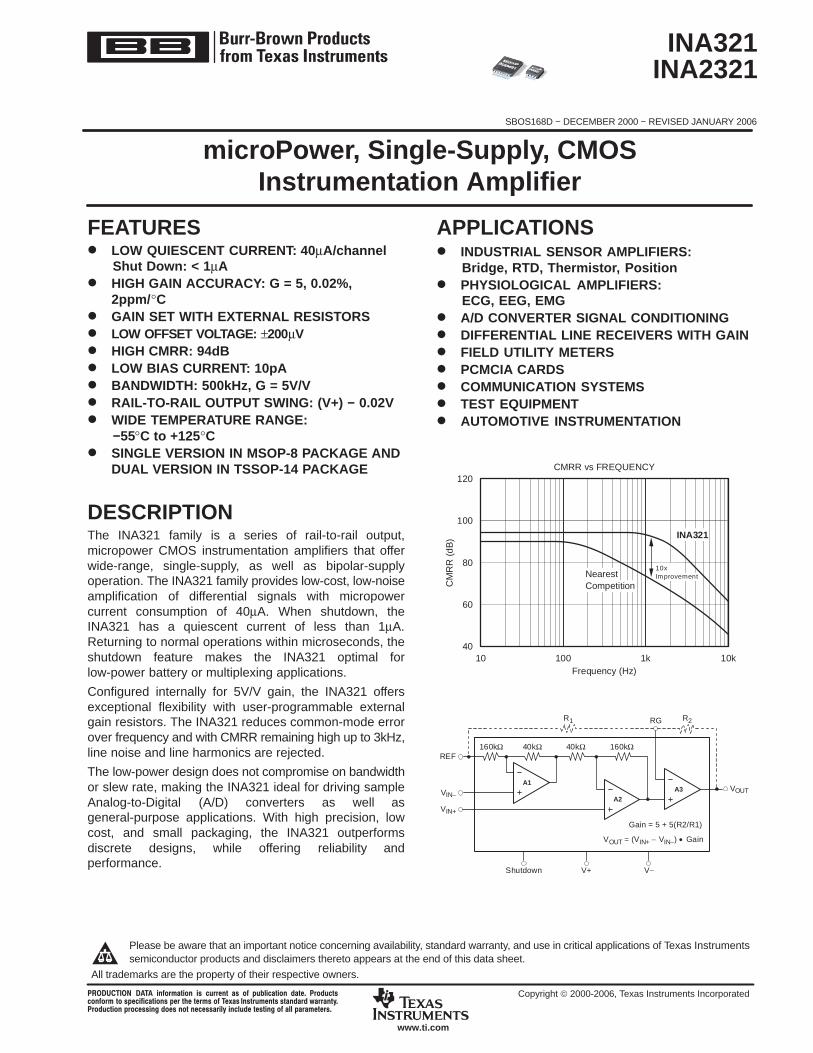
FEATURES LOW QUIESCENT CURRENT: 40µA/channel
Shut Down: < 1 µA HIGH GAIN ACCURACY: G = 5, 0.02%,
2ppm/ °C GAIN SET WITH EXTERNAL RESISTORS LOW OFFSET VOLTAGE: ±200µV HIGH CMRR: 94dB LOW BIAS CURRENT: 10pA BANDWIDTH: 500kHz, G = 5V/V RAIL-TO-RAIL OUTPUT SWING: (V+) − 0.02V WIDE TEMPERATURE RANGE:
−55°C to +125°C SINGLE VERSION IN MSOP-8 PACKAGE AND
DUAL VERSION IN TSSOP-14 PACKAGE
DESCRIPTIONThe INA321 family is a series of rail-to-rail output,micropower CMOS instrumentation amplifiers that offerwide-range, single-supply, as well as bipolar-supplyoperation. The INA321 family provides low-cost, low-noiseamplification of differential signals with micropowercurrent consumption of 40µA. When shutdown, theINA321 has a quiescent current of less than 1µA.Returning to normal operations within microseconds, theshutdown feature makes the INA321 optimal forlow-power battery or multiplexing applications.
Configured internally for 5V/V gain, the INA321 offersexceptional flexibility with user-programmable externalgain resistors. The INA321 reduces common-mode errorover frequency and with CMRR remaining high up to 3kHz,line noise and line harmonics are rejected.
The low-power design does not compromise on bandwidthor slew rate, making the INA321 ideal for driving sampleAnalog-to-Digital (A/D) converters as well asgeneral-purpose applications. With high precision, lowcost, and small packaging, the INA321 outperformsdiscrete designs, while offering reliability andperformance.
APPLICATIONS INDUSTRIAL SENSOR AMPLIFIERS:
Bridge, RTD, Thermistor, Position PHYSIOLOGICAL AMPLIFIERS:
ECG, EEG, EMG A/D CONVERTER SIGNAL CONDITIONING DIFFERENTIAL LINE RECEIVERS WITH GAIN FIELD UTILITY METERS PCMCIA CARDS COMMUNICATION SYSTEMS TEST EQUIPMENT AUTOMOTIVE INSTRUMENTATION
CMRR vs FREQUENCY
Frequency (Hz)
CM
RR
(dB
)
1k10 100 10k
120
100
80
60
40
INA321
NearestCompetition
10xImprovement
A2
A1A3
160kΩREF
VIN−
VIN+
40kΩ 40kΩ
Shutdown V+
VOUT
VOUT = (VIN+ − VIN−) • Gain
Gain = 5 + 5(R2/R1)
V−
R2R1 RG
160kΩ
INA321INA2321
SBOS168D − DECEMBER 2000 − REVISED JANUARY 2006
microPower, Single-Supply, CMOSInstrumentation Amplifier
www.ti.com
Copyright 2000-2006, Texas Instruments Incorporated
Please be aware that an important notice concerning availability, standard warranty, and use in critical applications of Texas Instrumentssemiconductor products and disclaimers thereto appears at the end of this data sheet.
All trademarks are the property of their respective owners.
! !

"#$#"#$
SBOS168D − DECEMBER 2000 − REVISED JANUARY 2006
www.ti.com
2
ABSOLUTE MAXIMUM RATINGS (1)
Supply Voltage, V+ to V− 7.5V. . . . . . . . . . . . . . . . . . . . . . . . . . . . . .
Signal Input Terminals Voltage(2) (V−) − (0.5V) to (V+) + (0.5V). . . Current(2) 10mA. . . . . . . . . . . . . . . . . . . . .
Output Short-Circuit(3) Continuous. . . . . . . . . . . . . . . . . . . . . . . . . . Operating Temperature −65°C to +150°C. . . . . . . . . . . . . . . . . . . . . . Storage Temperature −65°C to +150°C. . . . . . . . . . . . . . . . . . . . . . . . Junction Temperature +150°C. . . . . . . . . . . . . . . . . . . . . . . . . . . . . . .
(1) Stresses above these ratings may cause permanent damage.Exposure to absolute maximum conditions for extended periodsmay degrade device reliability. These are stress ratings only, andfunctional operation of the device at these or any other conditionsbeyond those specified is not supported.
(2) Input terminals are diode-clamped to the power-supply rails.Input signals that can swing more than 0.5V beyond the supplyrails should be current limited to 10mA or less.
(3) Short-circuit to ground, one amplifier per package.
ELECTROSTATICDISCHARGE SENSITIVITY
This integrated circuit can be damaged by ESD. Texas Instrumentsrecommends that all integrated circuits be handled with appropriateprecautions. Failure to observe proper handling and installationprocedures can cause damage.
ESD damage can range from subtle performance degradation tocomplete device failure. Precision integrated circuits may be moresusceptible to damage because very small parametric changes couldcause the device not to meet its published specifications.
PACKAGE/ORDERING INFORMATION (1)
PRODUCT PACKAGE-LEADPACKAGE
DESIGNATOR
SPECIFIEDTEMPERATURE
RANGE
PACKAGEMARKING
ORDERINGNUMBER
TRANSPORTMEDIA, QUANTITY
SINGLEINA321E MSOP-8 DGK −55°C to +125°C C21 INA321E/250 Tape and Reel, 250
″ ″ ″ ″ ″ INA321E/2K5 Tape and Reel, 2500
INA321EA MSOP-8 DGK −55°C to +125°C C21 INA321EA/250 Tape and Reel, 250″ ″ ″ ″ ″ INA321EA/2K5 Tape and Reel, 3000
DUALINA2321EA TSSOP-14 PW −55°C to +125°C INA2321EA INA2321EA/250 Tape and Reel, 250
″ ″ ″ ″ ″ INA2321EA/2K5 Tape and Reel, 2500
(1) For the most current package and ordering information, see the Package Option Addendum located at the end of this data sheet.
PIN CONFIGURATIONS
Top View
RG
VIN−
VIN+
V−
Shutdown
V+
VOUT
REF
INA321
MSOP−8 (E, EA)
1
2
3
4
8
7
6
5
1
2
3
4
5
6
7
14
13
12
11
10
9
8
Shutdown A
VOUTA
REFA
V+
REFB
VOUTB
Shutdown B
RGA
VIN−A
VIN+A
V−
VIN+B
VIN−B
RGB
INA2321
Dual, TSSOP−14 (EA)

"#$#"#$
SBOS168D − DECEMBER 2000 − REVISED JANUARY 2006
www.ti.com
3
ELECTRICAL CHARACTERISTICS: V S = +2.7V to +5.5V BOLDFACE limits apply over the specified temperature range, TA = −55C to +125C.At TA = +25°C, RL = 25kΩ, G = 25, and IA common = VS/2, unless otherwise noted.
INA321EINA321EAINA2321EA
PARAMETER CONDITIONS MIN TYP MAX MIN TYP MAX UNITINPUT
Input Offset Voltage, RTI VS = +5V ±0.2 ±0.5 ∗ 1 mV
Over Temperature VOS ±2.2 2.5 mV
vs Temperature dVOS/dT ±7 µV/°C
vs Power Supply PSRR VS = +2.7V to +5.5V ±50 ±200 ∗ ∗ µV/V
Over Temperature ±220 µV/V
Long-Term Stability ±0.4 ∗ µV/month
Input Impedance 1013 || 3 ∗ Ω || pF
Input Common-Mode Range VS = 2.7V 0.35 1.5 ∗ ∗ V
VS = 5V 0.55 3.8 ∗ ∗ V
Common-ModeRejection
CMRR VS = 5V, VCM = 0.55V to 3.8V 90 94 80 ∗ dB
Over Temperature VS = 5V, VCM = 0.55V to 3.8V 77 75 dB
VS = 2.7V, VCM = 0.35V to 1.5V 94 ∗ dB
Crosstalk, Dual 110 ∗ dB
INPUT BIAS CURRENT
Bias Current IB ±0.5 ±10 ∗ ∗ pA
Offset Current IOS ±0.5 ±10 ∗ ∗ pA
NOISE, RTI en RS = 0Ω
Voltage Noise: f = 10Hz 500 ∗ nV/√Hz
f = 100Hz 190 ∗ nV/√Hz
f = 1kHz 100 ∗ nV/√Hz
f = 0.1Hz to 10Hz 20 ∗ µVPPCurrent Noise: f = 1kHz 3 ∗ fA/√Hz
GAIN(1)
Gain Equation, Externally Set G > 5 G = 5 + 5 (R2/R1) ∗
Range of Gain 5 1000 ∗ ∗ V/V
Gain Error ±0.02 ±0.1 ∗ ∗ %
vs Temperature G = 5 ±2 ±10 ppm/°C
Nonlinearity G = 25, VS = 5V, VO = 0.05 to 4.95 ±0.001 ±0.010 ∗ ∗ % of FS
Over Temperature ±0.002 ±0.015 % of FS
OUTPUT
Output Voltage Swing from Rail(2, 5) G ≥ 10 50 25 ∗ ∗ mV
Over Temperature 50 mV
Capacitance Load Drive See Typical Characteristic(3) ∗ pF
Short-Circuit Current +ISC 8
−ISC 16 ∗ mA
NOTE: ∗ Specification is same as INA321E.(1) Does not include errors from external gain setting resistors.(2) Output voltage swings are measured between the output and power-supply rails.(3) See typical characteristic Percent Overshoot vs Load Capacitance.(4) See typical characteristic Shutdown Voltage vs Supply Voltage.(5) Output does not swing to positive rail if gain is less than 10.

"#$#"#$
SBOS168D − DECEMBER 2000 − REVISED JANUARY 2006
www.ti.com
4
ELECTRICAL CHARACTERISTICS: V S = +2.7V to +5.5V (continued)BOLDFACE limits apply over the specified temperature range, TA = −55C to +125C.At TA = +25°C, RL = 25kΩ, G = 25, and IA common = VS/2, unless otherwise noted.
INA321EAINA2321EAINA321E
PARAMETER UNITMAXTYPMINMAXTYPMINCONDITIONSFREQUENCY RESPONSE
Bandwidth, −3dB BW G = 5 500 ∗ kHz
Slew Rate SR VS = 5V, G = 25 0.4 ∗ V/µs
Settling Time, 0.1% tS G = 5, CL = 50pF, VO = 2V step 8 ∗ µs
0.01% 12 ∗ µs
Overload Recovery 50% Input Overload G = 25 2 ∗ µs
POWER SUPPLY
Specified Voltage Range +2.7 +5.5 ∗ ∗ V
Operating Voltage Range +2.5 to +5.5 ∗ V
Quiescent Current IQ per Channel, VSD > 2.5(4) 40 60 ∗ ∗ µA
Over Temperature 70 µA
Shutdown Quiescent Current ISD per Channel, VSD > 0.8(4) 0.01 1 ∗ ∗ µA
TEMPERATURE RANGE
Specified Range −55 +125 ∗ ∗ °C
Operating/Storage Range −65 +150 ∗ ∗ °C
Thermal Resistance JAMSOP-8, TSSOP-14
Surface-Mount150 ∗ °C/W
NOTE: ∗ Specification is same as INA321E.(1) Does not include errors from external gain setting resistors.(2) Output voltage swings are measured between the output and power-supply rails.(3) See typical characteristic Percent Overshoot vs Load Capacitance.(4) See typical characteristic Shutdown Voltage vs Supply Voltage.(5) Output does not swing to positive rail if gain is less than 10.

"#$#"#$
SBOS168D − DECEMBER 2000 − REVISED JANUARY 2006
www.ti.com
5
TYPICAL CHARACTERISTICS
At TA = +25°C, VS = 5V, VCM =1/2VS, RL = 25kΩ, and CL = 50pF, unless otherwise noted.
GAIN vs FREQUENCY
10
Gai
n(d
B)
Frequency (Hz)
100 1k 10k 100k 1M 10M
80
70
60
50
40
30
20
10
0
−10
−20
Gain = 500
Gain = 100
Gain = 25
Gain = 5
COMMON−MODE REJECTION RATIOvs FREQUENCY
10
CM
RR
(dB
)
Frequency (Hz)
100 1k 10k 100k
120
100
80
60
40
20
0
POWER−SUPPLY REJECTION RATIOvs FREQUENCY
1
PS
RR
(dB
)
Frequency (Hz)
10 100 1k 10k 100k
100
90
80
70
60
50
40
30
20
10
0
MAXIMUM OUTPUT VOLTAGE vs FREQUENCY
100
Max
imum
Out
put
Vo
ltage
(VP
P)
Frequency (Hz)
1k 10k 100k 1M 10M
6
5
4
3
2
1
0
VS = 5.5V
VS = 5.0V
VS = 2.7V
NOISE vs FREQUENCY
1
VN
OIS
E(n
V/√
Hz)
Frequency (Hz)
10 100 10k1k 100k
10k
1k
100
10
100
10
1
0.1
INoi
se(f
A/√
Hz)
0.1Hz TO 10Hz VOLTAGE NOISE
1s/div
10µ v
/div

"#$#"#$
SBOS168D − DECEMBER 2000 − REVISED JANUARY 2006
www.ti.com
6
TYPICAL CHARACTERISTICS (continued)
At TA = +25°C, VS = 5V, VCM =1/2VS, RL = 25kΩ, and CL = 50pF, unless otherwise noted.
To Positive Rail
To Negative Rail
OUTPUT SWING vs LOAD RESISTANCE
0
Sw
ing
−to
−R
ail(
mV
)
RLOAD (Ω)
20k 40k 60k 80k 100k
25
20
15
10
5
0
COMMON−MODE INPUT RANGEvs REFERENCE VOLTAGE
0
Out
put
Re
ferr
ed
toG
roun
d(V
)
Input Common−Mode Voltage (V)
1 2 3 4 5
6
5
4
3
2
1
0
Outside of Normal Operation
REFIncreasing
QUIESCENT CURRENT AND SHUTDOWN CURRENTvs POWER SUPPLY
I Q(µ
A)
I SD
(nA
)
Supply Voltage (V)
2.5 3 3.5 4 4.5 5 5.5
50
45
40
35
30
25
20
15
10
5
0
500
450
400
350
300
250
200
150
100
50
0
IQ
ISD
QUIESCENT CURRENT AND SHUTDOWN CURRENTvs TEMPERATURE
−75
I Q(µ
A)
600
500
400
300
200
100
0
I SD
(nA
)
Temperature (C)
−50 −25 0 25 50 75 100 125 150
605550454035302520151050
IQ
ISD
SHORT−CIRCUIT CURRENT vs POWER SUPPLY
I SC
(mA
)
Supply Voltage (V)
2.5 3 3.5 4 4.5 5 5.5
20
15
10
5
0
ISC+
ISC−
SHORT−CIRCUIT CURRENT vs TEMPERATURE
−75
I SC
(mA
)
Temperature (C)
−50 −25 0 25 50 75 100 125 150
30
25
20
15
10
5
0
ISC+
ISC−

"#$#"#$
SBOS168D − DECEMBER 2000 − REVISED JANUARY 2006
www.ti.com
7
TYPICAL CHARACTERISTICS (continued)
At TA = +25°C, VS = 5V, VCM =1/2VS, RL = 25kΩ, and CL = 50pF, unless otherwise noted.
SMALL−SIGNAL STEP RESPONSE (G = 5)
10µs/div
100
mV
/div
SMALL−SIGNAL STEP RESPONSE (G = 100)
50µs/div
50m
V/d
iv
SMALL−SIGNAL STEP RESPONSE(G = 5, CL = 1000pF)
10µs/div
100
mV
/div
SMALL−SIGNAL STEP RESPONSE(G = 100, CL = 1000pF)
50µs/div
50m
V/d
iv
SMALL−SIGNAL STEP RESPONSE(G = 100, CL = 5000pF)
50µs/div
50m
V/d
iv
50µs/div
1V
/div
LARGE−SIGNAL STEP RESPONSE(G = 25, CL = 50pF)

"#$#"#$
SBOS168D − DECEMBER 2000 − REVISED JANUARY 2006
www.ti.com
8
TYPICAL CHARACTERISTICS (continued)
At TA = +25°C, VS = 5V, VCM =1/2VS, RL = 25kΩ, and CL = 50pF, unless otherwise noted.
SETTLING TIME vs GAIN
1 10 100 1000
Gain (V/V)
Set
tling
Tim
e(µ
s)
100
90
80
70
60
50
40
30
20
10
0
Output 2VPPDifferentialInput Drive
0.01%
0.1%
PERCENT OVERSHOOT vs LOAD CAPACITANCE
10 100 1k 10k
Load Capacitance (pF)
Ove
rsh
oot
(%)
60
50
40
30
20
10
0
Output 100mVPPDifferentialInput Drive
G = 5
G = 25
SHUTDOWN VOLTAGE vs SUPPLY VOLTAGE
2.3
Shu
tdow
n(V
)
Supply Voltage (V)
3 3.5 4 4.5 5 5.5
3
2.5
2
1.5
1
0.5
0
Normal Operation Mode
Part Draws Below 1µA Quiescent Current
Operation in this Regionis not Recommended
Shutdown Mode
SHUTDOWN TRANSIENT BEHAVIOR
50µs/div
1V/d
iv
VSD
VOUT
25
20
15
10
5
0
−1
.0
−0
.9
−0
.8
−0
.7
−0
.6
−0
.5
−0
.4
−0
.3
−0
.2
−0
.1 0
0.1
0.2
0.3
0.4
0.5
0.6
0.7
0.8
0.9
1.0
Offset Voltage (mV)
Per
cent
age
ofA
mpl
ifier
s(%
)
OFFSET VOLTAGE PRODUCTION DISTRIBUTION20
18
16
14
12
10
8
6
4
2
0
− 20
− 18
− 16
− 14
− 12
− 10
−8
−6
−4
−2 0 2 4 6 8
10
12
14
16
18
20
Offset Voltage Drift (µV/C)
Per
cent
age
ofA
mp
lifie
rs(%
)
OFFSET VOLTAGE DRIFTPRODUCTION DISTRIBUTION

"#$#"#$
SBOS168D − DECEMBER 2000 − REVISED JANUARY 2006
www.ti.com
9
TYPICAL CHARACTERISTICS (continued)
At TA = +25°C, VS = 5V, VCM =1/2VS, RL = 25kΩ, and CL = 50pF, unless otherwise noted.
SLEW RATE vs TEMPERATURE
Sle
wR
ate
(V/µ
s)
Temperature (C)
−75 25−50 −25 0 50 75 100 125 150
1
0.8
0.6
0.4
0.2
0
INPUT BIAS CURRENT vs TEMPERATURE
−75 −50 −25 0 25 50 75 100 125 150
Temperature (C)
Inpu
tBia
sC
urre
nt(p
A)
10k
1k
100
10
0
0.1
CROSSTALK vs FREQUENCY
0.1 1 10 100 1k 10k 100k 1M
Frequency (Hz)
Cro
ssta
lk(d
B)
120
100
80
60
40
20
0
OUTPUT VOLTAGE SWING vs OUTPUT CURRENT
0 2 4 6 8 10 12 14 16 18 20 22 24
Output Current (mA)
Ou
tput
Vol
tage
(V)
5
4
3
2
1
0
−55C
− 55C
+125°C +25°C
+125°C +25°C

"#$#"#$
SBOS168D − DECEMBER 2000 − REVISED JANUARY 2006
www.ti.com
10
APPLICATIONS INFORMATIONThe INA321 is a modified version of the classic two op ampinstrumentation amplifier, with an additional gain amplifier.
Figure 1 shows the basic connections for the operation ofthe INA321 and INA2321. The power supply should becapacitively decoupled with 0.1µF capacitors as close tothe INA321 as possible for noisy or high-impedanceapplications.
The output is referred to the reference terminal, whichmust be at least 1.2V below the positive supply rail.
OPERATING VOLTAGE
The INA321 family is fully specified over a supply range of+2.7V to +5.5V, with key parameters assured over thetemperature range of −55°C to +125°C. Parameters thatvary significantly with operating conditions, such as loadconditions or temperature, are shown in the TypicalCharacteristics.
The INA321 may be operated on a single supply. Figure 2shows a bridge amplifier circuit operated from a single +5Vsupply. The bridge provides a small differential voltageriding on an input common-mode voltage.
160kΩ 40kΩ
40kΩ
160kΩ
3
2
5
1
78 4Also drawn in simplified form:
6
REF
0.1µF 0.1µF
RG
VIN−
VIN+
V−V+
A1A3
A2
VO = ((VIN+) − (VIN −)) • G
Short VOUT to RGfor G = 5
51050100
SHORT100kΩ90kΩ190kΩ
OPEN100kΩ10kΩ10kΩ
R2R1
Shutdown (For SingleSupply)
DESIRED GAIN(V/V) R1 R2
G = 5 + 5 (R2 / R1 )
INA3215
3
2
VOUT
8
7
6
4
1
V+Shutdown
RG
VIN−
V−
VIN+
REF
Figure 1. Basic Connections
BridgeSensor
+5V
NOTE: (1) REF should be adjusted for the desired output level,keeping in mind that the value of REF affects the common−modeinput range. See Typical Characteristics.
INA3215
3
2
VOUT
8
7
6
4
1
V+Shutdown
RG
VIN−
V−
VIN+
REF(1)
Figure 2. Bridge Amplifier of the INA321

"#$#"#$
SBOS168D − DECEMBER 2000 − REVISED JANUARY 2006
www.ti.com
11
SETTING THE GAIN
The ratio of R2 to R1, or the impedance between pins 1, 5,and 6, determines the gain of the INA321. With aninternally set gain of 5, the INA321 can be programmed forgains greater than 5 according to the following equation:
G = 5 + 5 (R2/R1)
The INA321 is designed to provide accurate gain, with gainerror assured to be less than 0.1%. Setting gain withmatching TC resistors will minimize gain drift. Errors fromexternal resistors will add directly to the gain error, andmay become dominant error sources.
INPUT COMMON-MODE RANGE
The upper limit of the common-mode input range is set bythe common-mode input range of the second amplifier, A2,to 1.2V below positive supply. Under most conditions, theamplifier operates beyond this point with reducedperformance. The lower limit of the input range is boundedby the output swing of amplifier A1, and is a function of thereference voltage according to the following equation:
VOA1 = 5/4 VCM — 1/4 VREF
(See Typical Characteristics for Input Common-ModeRange vs Reference Voltage).
REFERENCE
The reference terminal defines the zero output voltagelevel. In setting the reference voltage, the common-modeinput of A3 should be considered according to the followingequation:
VOA2 = VREF + 5 (VIN+ − VIN−)
For optimal operation, VOA2 should be less thanVDD − 1.2V.
The reference pin requires a low-impedance connection.As little as 160Ω in series with the reference pin willdegrade the CMRR to 80dB. The reference pin may beused to compensate for the offset voltage (see OffsetTrimming section). The reference voltage level alsoinfluences the common-mode input range (seeCommon-Mode Input Range section).
INPUT BIAS CURRENT RETURN
With a high input impedance of 1013Ω, the INA321 is idealfor use with high-impedance sources. The input biascurrent of less than 10pA makes the INA321 nearlyindependent of input impedance and ideal for low-powerapplications.
For proper operation, a path must be provided for inputbias currents for both inputs. Without input bias currentpaths, the inputs will float to a potential that exceedscommon-mode range and the input amplifier will saturate.
Figure 3 shows how bias current path can be provided inthe cases of microphone applications, thermistorapplications, ground returns, and dc-coupled resistivebridge applications.
47kΩ
Microphone,Hydrophone,etc.
Center−tapprovides biascurrent return
Bridge resistanceprovides biascurrent return
Transformer
BridgeAmplifier
BridgeSensor
VB(1)
VB(1)
VEX
NOTE: (1) VB is bias voltage withincommon−mode range, dependenton REF.
INA3215
3
2
8
7
6
4
1
V+Shutdown
VIN−
V−
VIN+
REF
INA3215
3
2
8
7
6
4
1
V+Shutdown
VIN−
V−
VIN+
REF
INA3215
3
2
8
7
6
4
1
V+Shutdown
VIN−
V−
VIN+
REF
VOUT
RG
VOUT
RG
VOUT
RG
Figure 3. Providing an Input Common-Mode Path
When differential source impedance is low, the biascurrent return path can be connected to one input. Withhigher source impedance, two equal resistors will providea balanced input. The advantages are lower input offsetvoltage due to bias current flowing through the sourceimpedance and better high-frequency gain.

"#$#"#$
SBOS168D − DECEMBER 2000 − REVISED JANUARY 2006
www.ti.com
12
OUTPUT BUFFERING
The INA321 is optimized for a load impedance of 10kΩ orgreater. For higher output current the INA321 can bebuffered using the OPA340, as shown in Figure 4. TheOPA340 can swing within 50mV of the supply rail, drivinga 600Ω load. The OPA340 is available in the tiny MSOP-8package.
OPA340 VOUT
+5V
0.1µF
0.1µF
INA3215
3
2
VOUT8
7
6
4
1
V+ Shutdown
RG
VIN−
V−
VIN+
REF
Figure 4. Output Buffering Circuit. Able to driveloads as low as 600 Ω.
SHUTDOWN MODE
The shutdown pin of the INA321 is nominally connected toV+. When the pin is pulled below 0.8V on a 5V supply, theINA321 goes into sleep mode within nanoseconds. Foractual shutdown threshold, see the Typical Characteristiccurve, Shutdown Voltage vs Supply Voltage. Drawing lessthan 1µA of current, and returning from sleep mode inmicroseconds, the shutdown feature is useful for portableapplications. Once in sleep-mode, the amplifier has highoutput impedance, making the INA321 suitable formultiplexing.
RAIL-TO-RAIL OUTPUT
A class AB output stage with common-source transistorsis used to achieve rail-to-rail output for gains of 10 orgreater. For resistive loads greater than 25kΩ, the outputvoltage can swing to within a few millivolts of the supply railwhile maintaining low gain error. For heavier loads andover temperature, see the Typical Characteristic curve,Output Voltage Swing vs Output Current. The INA321’s
low output impedance at high frequencies makes itsuitable for directly driving Capacitive Digital-to-Analog(CDAC) input A/D converters, as shown in Figure 5.
ADS7818or
ADS7822
12−Bits
+5V
INA3215
3
2
VOUT8
7
6
4
1
V+Shutdown
RG
VIN−
V−
VIN+
REF
fS < 100kHz
Figure 5. INA321 Directly Drives aCapacitive-Input, A/D Converter
OFFSET TRIMMING
The INA321 is laser-trimmed for low offset voltage. In theevent that external offset adjustment is required, the offsetcan be adjusted by applying a correction voltage to thereference terminal. Figure 6 shows an optional circuit fortrimming offset voltage. The voltage applied to the REFterminal is added to the output signal. The gain from REFto VOUT is +1. An op-amp buffer is used to provide lowimpedance at the REF terminal to preserve goodcommon-mode rejection.
OPA336AdjustableVoltage
INA3215
3
2
VOUT
8
7
6
4
1
V+Shutdown
RG
VIN−
V−
VIN+
REF(1)
NOTE: (1) REF should be adjusted for the desired output level.The value of REF affects the common−mode input range.
Figure 6. Optional Offset Trimming Voltage

"#$#"#$
SBOS168D − DECEMBER 2000 − REVISED JANUARY 2006
www.ti.com
13
INPUT PROTECTIONDevice inputs are protected by ESD diodes that willconduct if the input voltages exceed the power supplies bymore than 500mV. Momentary voltages greater than500mV beyond the power supply can be tolerated if thecurrent through the input pins is limited to 10mA. This iseasily accomplished with input resistor RLIM, as shown inFigure 7. Many input signals are inherently current-limitedto less than 10mA; therefore, a limiting resistor is notrequired.
RLIM
RLIM
IOVERLOAD10mA max
INA3215
3
2
VOUT
8
7
6
4
1
V+Shutdown
RG
VIN−
V−
VIN+
REF
Figure 7. Input Protection
OFFSET VOLTAGE ERROR CALCULATIONThe offset voltage (VOS) of the INA321E is specified at amaximum of 500µV with a +5V power supply and thecommon-mode voltage at VS/2. Additional specificationsfor power-supply rejection and common-mode rejectionare provided to allow the user to easily calculateworst-case expected offset under the conditions of a givenapplication.
Power-Supply Rejection Ratio (PSRR) is specified inµV/V. For the INA321, worst-case PSRR is 200µV/V,which means for each volt of change in power supply, theoffset may shift up to 200µV. Common-Mode RejectionRatio (CMRR) is specified in dB, which can be convertedto µV/V using the following equation:
CMRR (in µV/V) = 10[(CMRR in dB)/—20] • 106
For the INA321, the worst-case CMRR over the specifiedcommon-mode range is 90dB (at G = 25) or about 30µV/V.This means that for every volt of change in common-mode,the offset will shift less than 30µV.
These numbers can be used to calculate excursions fromthe specified offset voltage under different applicationconditions. For example, an application might configurethe amplifier with a 3.3V supply with 1V common-mode.This configuration varies from the specified configuration,representing a 1.7V variation in power supply (5V in theoffset specification versus 3.3V in the application) and a0.65V variation in common-mode voltage from thespecified VS/2.
Calculation of the worst-case expected offset would be asfollows:
Adjusted VOS = Maximum specified VOS +(power-supply variation) • PSRR +(common-mode variation) • CMRR
VOS = 0.5mV + (1.7V • 200µV) + (0.65V • 30µV)= ±0.860mV
However, the typical value will be smaller, as seen in theTypical Characteristics.
FEEDBACK CAPACITOR IMPROVES RESPONSE
For optimum settling time and stability withhigh-impedance feedback networks, it may be necessaryto add a feedback capacitor across the feedback resistor,RF, as shown in Figure 8. This capacitor compensates forthe zero created by the feedback network impedance andthe INA321’s RG-pin input capacitance (and any parasiticlayout capacitance). The effect becomes more significantwith higher impedance networks. Also, RX and CL can beadded to reduce high-frequency noise.
INA321
V+
VOUT
RIN
RIN • CIN = RF • CF
RF
RX
CL
CIN
Where CIN is equal to the INA321 input capacitance(approximately 3pF) plus any parastic layout capacitance.
5
3
2
8
7
6
4
1
Shutdown
RGVIN−
V−
VIN+
REF
CF
Figure 8. Feedback Capacitor Improves DynamicPerformance
It is suggested that a variable capacitor be used for thefeedback capacitor since input capacitance may varybetween instrumentation amplifiers, and layoutcapacitance is difficult to determine. For the circuit shownin Figure 8, the value of the variable feedback capacitorshould be chosen by the following equation:
RIN • CIN = RF • CF
where CIN is equal to the INA321’s RG-pin inputcapacitance (typically 3pF) plus the layout capacitance.The capacitor can be varied until optimum performance isobtained.

"#$#"#$
SBOS168D − DECEMBER 2000 − REVISED JANUARY 2006
www.ti.com
14
APPLICATION CIRCUITSMedical ECG Applications
Figure 9 shows the INA321 configured to serve as alow-cost ECG amplifier, suitable for moderate accuracyheart-rate applications such as fitness equipment. Theinput signals are obtained from the left and right arms of thepatient. The common-mode voltage is set by two 2MΩ resistors. This potential, through a buffer, provides an
optional right leg drive. Filtering can be modified to suitapplication needs by changing the capacitor value of theoutput filter.Low-Power, Single-Supply Data AcquisitionSystems
Refer to Figure 5 to see the INA321 configured to drive anADS7818. Functioning at frequencies of up to 500kHz, theINA321 is ideal for low-power data acquisition.
OPA336
OPA336
OPA336Right Arm
Left Arm
OPA336
1MΩ
REF
1MΩ
1MΩ
10kΩ
10kΩShieldDrive 390kΩ
10kΩ
2kΩ
2kΩ
1.6nF0.1µF
100kΩ
100kΩShield
+5V
VR
VR
VR = +2.5V
2MΩ 2MΩ
RightLeg
VR
INA3215
3
2
8
7
6
4
1
V+Shutdown
RG
VIN−
V−
VIN+
VOUT PUT
100kΩ
Figure 9. Simplified ECG Circuit for Medical Applications
PACKAGE OPTION ADDENDUM
www.ti.com 11-Apr-2013
Addendum-Page 1
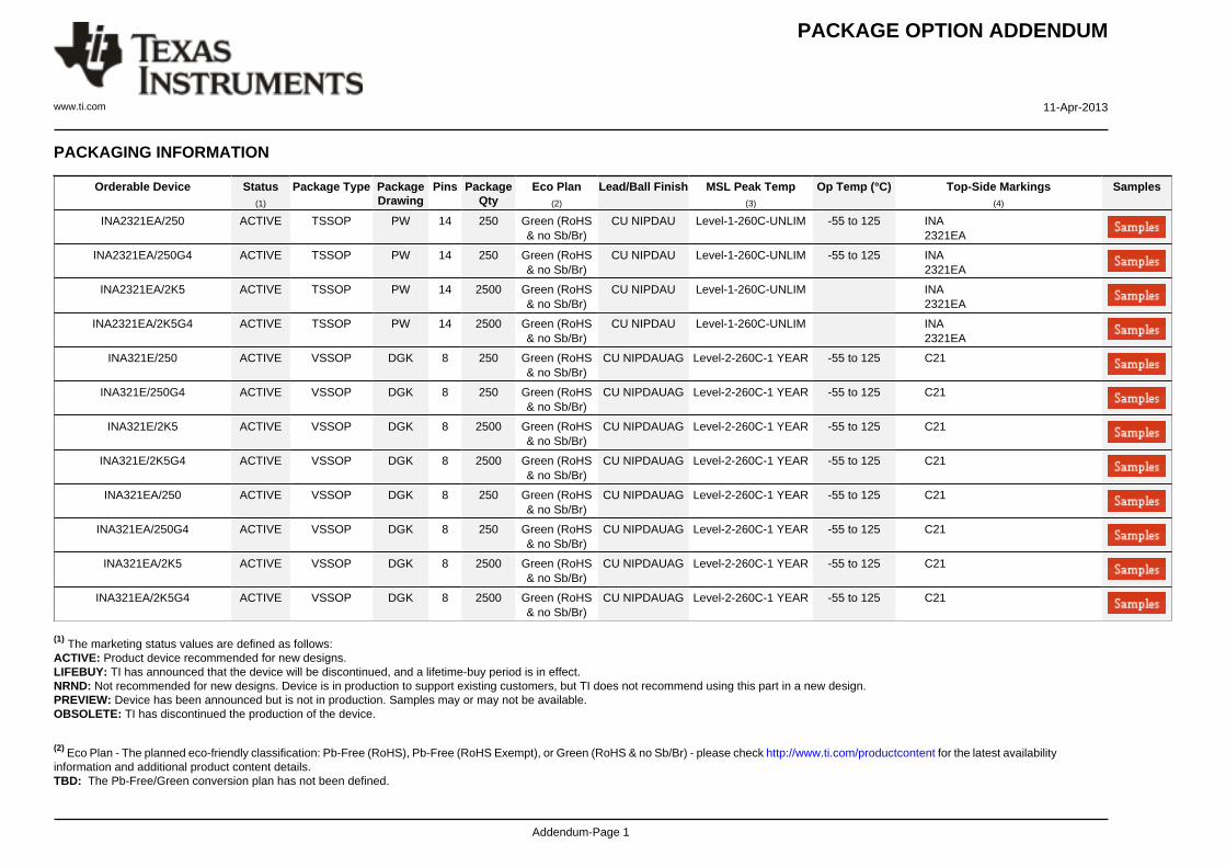
PACKAGING INFORMATION
Orderable Device Status(1)
Package Type PackageDrawing
Pins PackageQty
Eco Plan(2)
Lead/Ball Finish MSL Peak Temp(3)
Op Temp (°C) Top-Side Markings(4)
Samples
INA2321EA/250 ACTIVE TSSOP PW 14 250 Green (RoHS& no Sb/Br)
CU NIPDAU Level-1-260C-UNLIM -55 to 125 INA2321EA
INA2321EA/250G4 ACTIVE TSSOP PW 14 250 Green (RoHS& no Sb/Br)
CU NIPDAU Level-1-260C-UNLIM -55 to 125 INA2321EA
INA2321EA/2K5 ACTIVE TSSOP PW 14 2500 Green (RoHS& no Sb/Br)
CU NIPDAU Level-1-260C-UNLIM INA2321EA
INA2321EA/2K5G4 ACTIVE TSSOP PW 14 2500 Green (RoHS& no Sb/Br)
CU NIPDAU Level-1-260C-UNLIM INA2321EA
INA321E/250 ACTIVE VSSOP DGK 8 250 Green (RoHS& no Sb/Br)
CU NIPDAUAG Level-2-260C-1 YEAR -55 to 125 C21
INA321E/250G4 ACTIVE VSSOP DGK 8 250 Green (RoHS& no Sb/Br)
CU NIPDAUAG Level-2-260C-1 YEAR -55 to 125 C21
INA321E/2K5 ACTIVE VSSOP DGK 8 2500 Green (RoHS& no Sb/Br)
CU NIPDAUAG Level-2-260C-1 YEAR -55 to 125 C21
INA321E/2K5G4 ACTIVE VSSOP DGK 8 2500 Green (RoHS& no Sb/Br)
CU NIPDAUAG Level-2-260C-1 YEAR -55 to 125 C21
INA321EA/250 ACTIVE VSSOP DGK 8 250 Green (RoHS& no Sb/Br)
CU NIPDAUAG Level-2-260C-1 YEAR -55 to 125 C21
INA321EA/250G4 ACTIVE VSSOP DGK 8 250 Green (RoHS& no Sb/Br)
CU NIPDAUAG Level-2-260C-1 YEAR -55 to 125 C21
INA321EA/2K5 ACTIVE VSSOP DGK 8 2500 Green (RoHS& no Sb/Br)
CU NIPDAUAG Level-2-260C-1 YEAR -55 to 125 C21
INA321EA/2K5G4 ACTIVE VSSOP DGK 8 2500 Green (RoHS& no Sb/Br)
CU NIPDAUAG Level-2-260C-1 YEAR -55 to 125 C21
(1) The marketing status values are defined as follows:ACTIVE: Product device recommended for new designs.LIFEBUY: TI has announced that the device will be discontinued, and a lifetime-buy period is in effect.NRND: Not recommended for new designs. Device is in production to support existing customers, but TI does not recommend using this part in a new design.PREVIEW: Device has been announced but is not in production. Samples may or may not be available.OBSOLETE: TI has discontinued the production of the device.
(2) Eco Plan - The planned eco-friendly classification: Pb-Free (RoHS), Pb-Free (RoHS Exempt), or Green (RoHS & no Sb/Br) - please check http://www.ti.com/productcontent for the latest availabilityinformation and additional product content details.TBD: The Pb-Free/Green conversion plan has not been defined.

PACKAGE OPTION ADDENDUM
www.ti.com 11-Apr-2013
Addendum-Page 2
Pb-Free (RoHS): TI's terms "Lead-Free" or "Pb-Free" mean semiconductor products that are compatible with the current RoHS requirements for all 6 substances, including the requirement thatlead not exceed 0.1% by weight in homogeneous materials. Where designed to be soldered at high temperatures, TI Pb-Free products are suitable for use in specified lead-free processes.Pb-Free (RoHS Exempt): This component has a RoHS exemption for either 1) lead-based flip-chip solder bumps used between the die and package, or 2) lead-based die adhesive used betweenthe die and leadframe. The component is otherwise considered Pb-Free (RoHS compatible) as defined above.Green (RoHS & no Sb/Br): TI defines "Green" to mean Pb-Free (RoHS compatible), and free of Bromine (Br) and Antimony (Sb) based flame retardants (Br or Sb do not exceed 0.1% by weightin homogeneous material)
(3) MSL, Peak Temp. -- The Moisture Sensitivity Level rating according to the JEDEC industry standard classifications, and peak solder temperature.
(4) Multiple Top-Side Markings will be inside parentheses. Only one Top-Side Marking contained in parentheses and separated by a "~" will appear on a device. If a line is indented then it is acontinuation of the previous line and the two combined represent the entire Top-Side Marking for that device.
Important Information and Disclaimer:The information provided on this page represents TI's knowledge and belief as of the date that it is provided. TI bases its knowledge and belief on informationprovided by third parties, and makes no representation or warranty as to the accuracy of such information. Efforts are underway to better integrate information from third parties. TI has taken andcontinues to take reasonable steps to provide representative and accurate information but may not have conducted destructive testing or chemical analysis on incoming materials and chemicals.TI and TI suppliers consider certain information to be proprietary, and thus CAS numbers and other limited information may not be available for release.
In no event shall TI's liability arising out of such information exceed the total purchase price of the TI part(s) at issue in this document sold by TI to Customer on an annual basis.

TAPE AND REEL INFORMATION
*All dimensions are nominal
Device PackageType
PackageDrawing
Pins SPQ ReelDiameter
(mm)
ReelWidth
W1 (mm)
A0(mm)
B0(mm)
K0(mm)
P1(mm)
W(mm)
Pin1Quadrant
INA2321EA/250 TSSOP PW 14 250 180.0 12.4 6.9 5.6 1.6 8.0 12.0 Q1
INA321E/250 VSSOP DGK 8 250 180.0 12.4 5.3 3.4 1.4 8.0 12.0 Q1
INA321E/2K5 VSSOP DGK 8 2500 330.0 12.4 5.3 3.4 1.4 8.0 12.0 Q1
INA321EA/250 VSSOP DGK 8 250 180.0 12.4 5.3 3.4 1.4 8.0 12.0 Q1
INA321EA/2K5 VSSOP DGK 8 2500 330.0 12.4 5.3 3.4 1.4 8.0 12.0 Q1
PACKAGE MATERIALS INFORMATION
www.ti.com 8-Apr-2013
Pack Materials-Page 1

*All dimensions are nominal
Device Package Type Package Drawing Pins SPQ Length (mm) Width (mm) Height (mm)
INA2321EA/250 TSSOP PW 14 250 210.0 185.0 35.0
INA321E/250 VSSOP DGK 8 250 210.0 185.0 35.0
INA321E/2K5 VSSOP DGK 8 2500 367.0 367.0 35.0
INA321EA/250 VSSOP DGK 8 250 210.0 185.0 35.0
INA321EA/2K5 VSSOP DGK 8 2500 367.0 367.0 35.0
PACKAGE MATERIALS INFORMATION
www.ti.com 8-Apr-2013
Pack Materials-Page 2


IMPORTANT NOTICE
Texas Instruments Incorporated and its subsidiaries (TI) reserve the right to make corrections, enhancements, improvements and otherchanges to its semiconductor products and services per JESD46, latest issue, and to discontinue any product or service per JESD48, latestissue. Buyers should obtain the latest relevant information before placing orders and should verify that such information is current andcomplete. All semiconductor products (also referred to herein as “components”) are sold subject to TI’s terms and conditions of salesupplied at the time of order acknowledgment.TI warrants performance of its components to the specifications applicable at the time of sale, in accordance with the warranty in TI’s termsand conditions of sale of semiconductor products. Testing and other quality control techniques are used to the extent TI deems necessaryto support this warranty. Except where mandated by applicable law, testing of all parameters of each component is not necessarilyperformed.TI assumes no liability for applications assistance or the design of Buyers’ products. Buyers are responsible for their products andapplications using TI components. To minimize the risks associated with Buyers’ products and applications, Buyers should provideadequate design and operating safeguards.TI does not warrant or represent that any license, either express or implied, is granted under any patent right, copyright, mask work right, orother intellectual property right relating to any combination, machine, or process in which TI components or services are used. Informationpublished by TI regarding third-party products or services does not constitute a license to use such products or services or a warranty orendorsement thereof. Use of such information may require a license from a third party under the patents or other intellectual property of thethird party, or a license from TI under the patents or other intellectual property of TI.Reproduction of significant portions of TI information in TI data books or data sheets is permissible only if reproduction is without alterationand is accompanied by all associated warranties, conditions, limitations, and notices. TI is not responsible or liable for such altereddocumentation. Information of third parties may be subject to additional restrictions.Resale of TI components or services with statements different from or beyond the parameters stated by TI for that component or servicevoids all express and any implied warranties for the associated TI component or service and is an unfair and deceptive business practice.TI is not responsible or liable for any such statements.Buyer acknowledges and agrees that it is solely responsible for compliance with all legal, regulatory and safety-related requirementsconcerning its products, and any use of TI components in its applications, notwithstanding any applications-related information or supportthat may be provided by TI. Buyer represents and agrees that it has all the necessary expertise to create and implement safeguards whichanticipate dangerous consequences of failures, monitor failures and their consequences, lessen the likelihood of failures that might causeharm and take appropriate remedial actions. Buyer will fully indemnify TI and its representatives against any damages arising out of the useof any TI components in safety-critical applications.In some cases, TI components may be promoted specifically to facilitate safety-related applications. With such components, TI’s goal is tohelp enable customers to design and create their own end-product solutions that meet applicable functional safety standards andrequirements. Nonetheless, such components are subject to these terms.No TI components are authorized for use in FDA Class III (or similar life-critical medical equipment) unless authorized officers of the partieshave executed a special agreement specifically governing such use.Only those TI components which TI has specifically designated as military grade or “enhanced plastic” are designed and intended for use inmilitary/aerospace applications or environments. Buyer acknowledges and agrees that any military or aerospace use of TI componentswhich have not been so designated is solely at the Buyer's risk, and that Buyer is solely responsible for compliance with all legal andregulatory requirements in connection with such use.TI has specifically designated certain components as meeting ISO/TS16949 requirements, mainly for automotive use. In any case of use ofnon-designated products, TI will not be responsible for any failure to meet ISO/TS16949.
Products ApplicationsAudio www.ti.com/audio Automotive and Transportation www.ti.com/automotiveAmplifiers amplifier.ti.com Communications and Telecom www.ti.com/communicationsData Converters dataconverter.ti.com Computers and Peripherals www.ti.com/computersDLP® Products www.dlp.com Consumer Electronics www.ti.com/consumer-appsDSP dsp.ti.com Energy and Lighting www.ti.com/energyClocks and Timers www.ti.com/clocks Industrial www.ti.com/industrialInterface interface.ti.com Medical www.ti.com/medicalLogic logic.ti.com Security www.ti.com/securityPower Mgmt power.ti.com Space, Avionics and Defense www.ti.com/space-avionics-defenseMicrocontrollers microcontroller.ti.com Video and Imaging www.ti.com/videoRFID www.ti-rfid.comOMAP Applications Processors www.ti.com/omap TI E2E Community e2e.ti.comWireless Connectivity www.ti.com/wirelessconnectivity
Mailing Address: Texas Instruments, Post Office Box 655303, Dallas, Texas 75265Copyright © 2015, Texas Instruments Incorporated