Embed Size (px)
Citation preview
Z80180
Microprocessor Unit
ZiLOG WorldwidTelephone:
Product Specification
PS014004-1106PS014004-1106
e Headquarters • 532 Race Street • San Jose, CA 95126 408.558.8500 • Fax: 408.558.8300 • www.zilog.com
This publication is subject to replacement by a later edition. To determine whether a later edition exists, or to request copies of publications, contact:
ZiLOG Worldwide Headquarters532 Race StreetSan Jose, CA 95126-3432Telephone: 408.558.8500Fax: 408.558.8300www.zilog.com
ZiLOG is a registered trademark of ZiLOG Inc. in the United States and in other countries. All other products and/or service names mentioned herein may be trademarks of the companies with which they are associated.
Document Disclaimer©2006 by ZiLOG, Inc. All rights reserved. Information in this publication concerning the devices, applications, or technology described is intended to suggest possible uses and may be superseded. ZiLOG, INC. DOES NOT ASSUME LIABILITY FOR OR PROVIDE A REPRESENTATION OF ACCURACY OF THE INFORMATION, DEVICES, OR TECHNOLOGY DESCRIBED IN THIS DOCUMENT. ZiLOG ALSO DOES NOT ASSUME LIABILITY FOR INTELLECTUAL PROPERTY INFRINGEMENT RELATED IN ANY MANNER TO USE OF INFORMATION, DEVICES, OR TECHNOLOGY DESCRIBED HEREIN OR OTHERWISE. Devices sold by ZiLOG, Inc. are covered by warranty and limitation of liability provisions appearing in the ZiLOG, Inc. Terms and Conditions of Sale. ZiLOG, Inc. makes no warranty of merchantability or fitness for any purpose. Except with the express written approval of ZiLOG, use of information, devices, or technology as critical components of life support systems is not authorized. No licenses are conveyed, implicitly or otherwise, by this document under any intellectual property rights.
PS014004-1106
Z80180Microprocessor Unit
iii
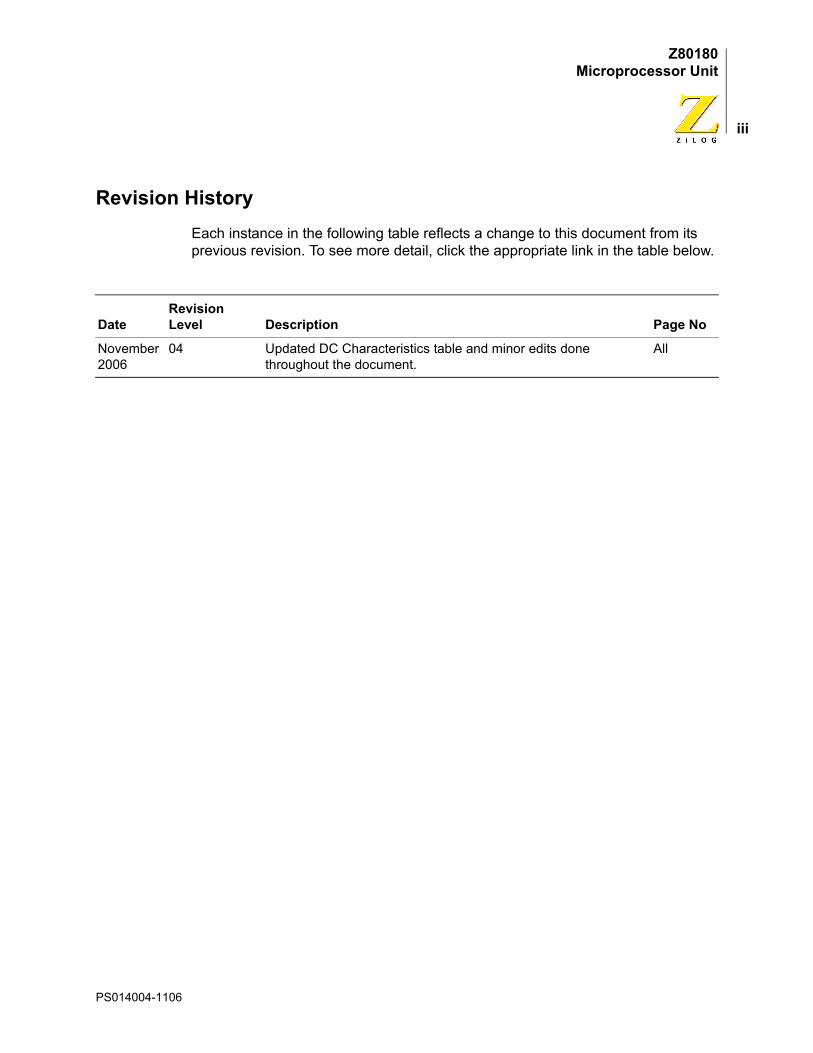
Revision HistoryEach instance in the following table reflects a change to this document from its previous revision. To see more detail, click the appropriate link in the table below.
DateRevision Level Description Page No
November 2006
04 Updated DC Characteristics table and minor edits done throughout the document.
All
PS014004-1106

Z80180Microprocessor Unit
iv
PS014004-1106
Z80180Microprocessor Unit
v
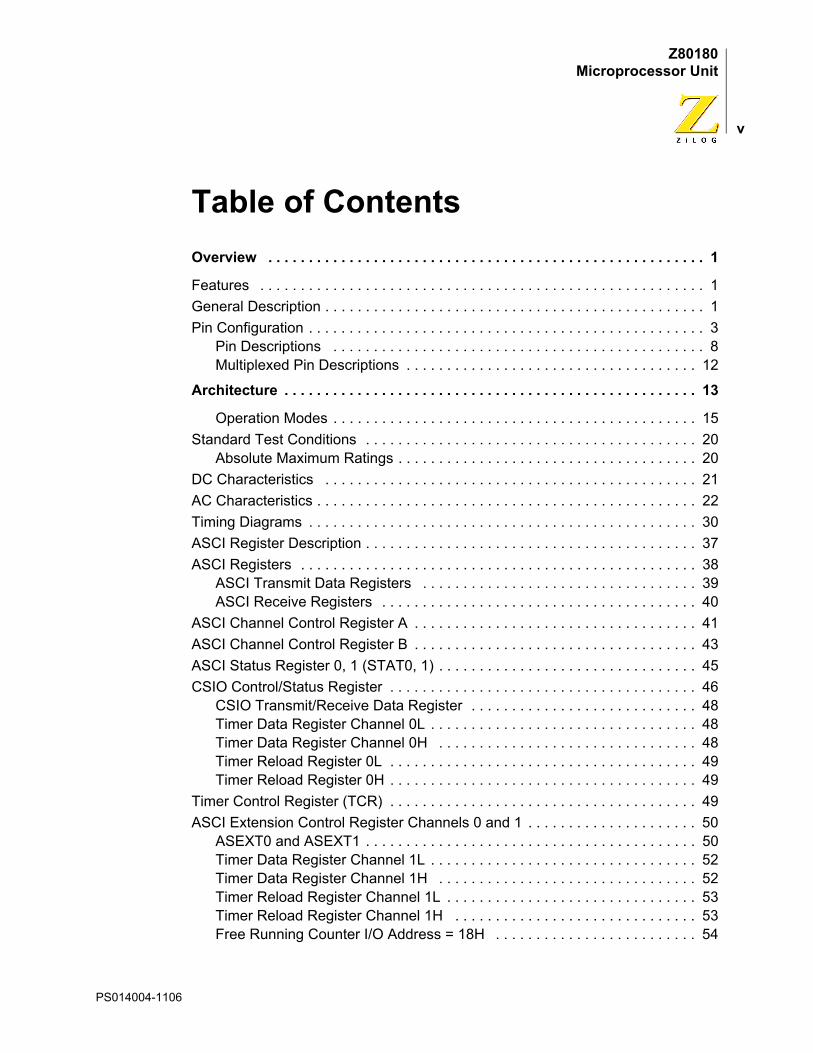
Table of ContentsOverview . . . . . . . . . . . . . . . . . . . . . . . . . . . . . . . . . . . . . . . . . . . . . . . . . . . . . . 1
Features . . . . . . . . . . . . . . . . . . . . . . . . . . . . . . . . . . . . . . . . . . . . . . . . . . . . . . . 1General Description . . . . . . . . . . . . . . . . . . . . . . . . . . . . . . . . . . . . . . . . . . . . . . . 1Pin Configuration . . . . . . . . . . . . . . . . . . . . . . . . . . . . . . . . . . . . . . . . . . . . . . . . . 3
Pin Descriptions . . . . . . . . . . . . . . . . . . . . . . . . . . . . . . . . . . . . . . . . . . . . . . 8Multiplexed Pin Descriptions . . . . . . . . . . . . . . . . . . . . . . . . . . . . . . . . . . . . 12
Architecture . . . . . . . . . . . . . . . . . . . . . . . . . . . . . . . . . . . . . . . . . . . . . . . . . . . 13
Operation Modes . . . . . . . . . . . . . . . . . . . . . . . . . . . . . . . . . . . . . . . . . . . . . 15Standard Test Conditions . . . . . . . . . . . . . . . . . . . . . . . . . . . . . . . . . . . . . . . . . 20
Absolute Maximum Ratings . . . . . . . . . . . . . . . . . . . . . . . . . . . . . . . . . . . . . 20DC Characteristics . . . . . . . . . . . . . . . . . . . . . . . . . . . . . . . . . . . . . . . . . . . . . . 21AC Characteristics . . . . . . . . . . . . . . . . . . . . . . . . . . . . . . . . . . . . . . . . . . . . . . . 22Timing Diagrams . . . . . . . . . . . . . . . . . . . . . . . . . . . . . . . . . . . . . . . . . . . . . . . . 30ASCI Register Description . . . . . . . . . . . . . . . . . . . . . . . . . . . . . . . . . . . . . . . . . 37ASCI Registers . . . . . . . . . . . . . . . . . . . . . . . . . . . . . . . . . . . . . . . . . . . . . . . . . 38
ASCI Transmit Data Registers . . . . . . . . . . . . . . . . . . . . . . . . . . . . . . . . . . 39ASCI Receive Registers . . . . . . . . . . . . . . . . . . . . . . . . . . . . . . . . . . . . . . . 40
ASCI Channel Control Register A . . . . . . . . . . . . . . . . . . . . . . . . . . . . . . . . . . . 41ASCI Channel Control Register B . . . . . . . . . . . . . . . . . . . . . . . . . . . . . . . . . . . 43ASCI Status Register 0, 1 (STAT0, 1) . . . . . . . . . . . . . . . . . . . . . . . . . . . . . . . . 45CSIO Control/Status Register . . . . . . . . . . . . . . . . . . . . . . . . . . . . . . . . . . . . . . 46
CSIO Transmit/Receive Data Register . . . . . . . . . . . . . . . . . . . . . . . . . . . . 48Timer Data Register Channel 0L . . . . . . . . . . . . . . . . . . . . . . . . . . . . . . . . . 48Timer Data Register Channel 0H . . . . . . . . . . . . . . . . . . . . . . . . . . . . . . . . 48Timer Reload Register 0L . . . . . . . . . . . . . . . . . . . . . . . . . . . . . . . . . . . . . . 49Timer Reload Register 0H . . . . . . . . . . . . . . . . . . . . . . . . . . . . . . . . . . . . . . 49
Timer Control Register (TCR) . . . . . . . . . . . . . . . . . . . . . . . . . . . . . . . . . . . . . . 49ASCI Extension Control Register Channels 0 and 1 . . . . . . . . . . . . . . . . . . . . . 50
ASEXT0 and ASEXT1 . . . . . . . . . . . . . . . . . . . . . . . . . . . . . . . . . . . . . . . . . 50Timer Data Register Channel 1L . . . . . . . . . . . . . . . . . . . . . . . . . . . . . . . . . 52Timer Data Register Channel 1H . . . . . . . . . . . . . . . . . . . . . . . . . . . . . . . . 52Timer Reload Register Channel 1L . . . . . . . . . . . . . . . . . . . . . . . . . . . . . . . 53Timer Reload Register Channel 1H . . . . . . . . . . . . . . . . . . . . . . . . . . . . . . 53Free Running Counter I/O Address = 18H . . . . . . . . . . . . . . . . . . . . . . . . . 54
PS014004-1106
Z80180Microprocessor Unit
vi
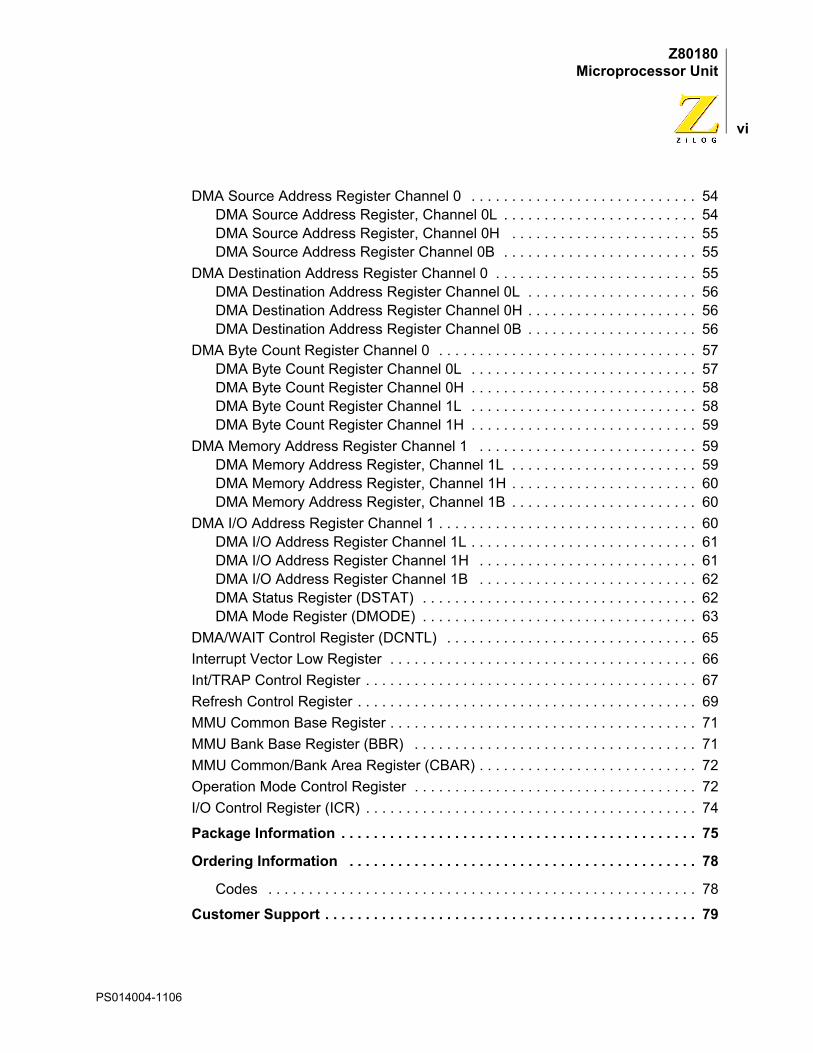
DMA Source Address Register Channel 0 . . . . . . . . . . . . . . . . . . . . . . . . . . . . 54DMA Source Address Register, Channel 0L . . . . . . . . . . . . . . . . . . . . . . . . 54DMA Source Address Register, Channel 0H . . . . . . . . . . . . . . . . . . . . . . . 55DMA Source Address Register Channel 0B . . . . . . . . . . . . . . . . . . . . . . . . 55
DMA Destination Address Register Channel 0 . . . . . . . . . . . . . . . . . . . . . . . . . 55DMA Destination Address Register Channel 0L . . . . . . . . . . . . . . . . . . . . . 56DMA Destination Address Register Channel 0H . . . . . . . . . . . . . . . . . . . . . 56DMA Destination Address Register Channel 0B . . . . . . . . . . . . . . . . . . . . . 56
DMA Byte Count Register Channel 0 . . . . . . . . . . . . . . . . . . . . . . . . . . . . . . . . 57DMA Byte Count Register Channel 0L . . . . . . . . . . . . . . . . . . . . . . . . . . . . 57DMA Byte Count Register Channel 0H . . . . . . . . . . . . . . . . . . . . . . . . . . . . 58DMA Byte Count Register Channel 1L . . . . . . . . . . . . . . . . . . . . . . . . . . . . 58DMA Byte Count Register Channel 1H . . . . . . . . . . . . . . . . . . . . . . . . . . . . 59
DMA Memory Address Register Channel 1 . . . . . . . . . . . . . . . . . . . . . . . . . . . 59DMA Memory Address Register, Channel 1L . . . . . . . . . . . . . . . . . . . . . . . 59DMA Memory Address Register, Channel 1H . . . . . . . . . . . . . . . . . . . . . . . 60DMA Memory Address Register, Channel 1B . . . . . . . . . . . . . . . . . . . . . . . 60
DMA I/O Address Register Channel 1 . . . . . . . . . . . . . . . . . . . . . . . . . . . . . . . . 60DMA I/O Address Register Channel 1L . . . . . . . . . . . . . . . . . . . . . . . . . . . . 61DMA I/O Address Register Channel 1H . . . . . . . . . . . . . . . . . . . . . . . . . . . 61DMA I/O Address Register Channel 1B . . . . . . . . . . . . . . . . . . . . . . . . . . . 62DMA Status Register (DSTAT) . . . . . . . . . . . . . . . . . . . . . . . . . . . . . . . . . . 62DMA Mode Register (DMODE) . . . . . . . . . . . . . . . . . . . . . . . . . . . . . . . . . . 63
DMA/WAIT Control Register (DCNTL) . . . . . . . . . . . . . . . . . . . . . . . . . . . . . . . 65Interrupt Vector Low Register . . . . . . . . . . . . . . . . . . . . . . . . . . . . . . . . . . . . . . 66Int/TRAP Control Register . . . . . . . . . . . . . . . . . . . . . . . . . . . . . . . . . . . . . . . . . 67Refresh Control Register . . . . . . . . . . . . . . . . . . . . . . . . . . . . . . . . . . . . . . . . . . 69MMU Common Base Register . . . . . . . . . . . . . . . . . . . . . . . . . . . . . . . . . . . . . . 71MMU Bank Base Register (BBR) . . . . . . . . . . . . . . . . . . . . . . . . . . . . . . . . . . . 71MMU Common/Bank Area Register (CBAR) . . . . . . . . . . . . . . . . . . . . . . . . . . . 72Operation Mode Control Register . . . . . . . . . . . . . . . . . . . . . . . . . . . . . . . . . . . 72I/O Control Register (ICR) . . . . . . . . . . . . . . . . . . . . . . . . . . . . . . . . . . . . . . . . . 74
Package Information . . . . . . . . . . . . . . . . . . . . . . . . . . . . . . . . . . . . . . . . . . . . 75
Ordering Information . . . . . . . . . . . . . . . . . . . . . . . . . . . . . . . . . . . . . . . . . . . 78
Codes . . . . . . . . . . . . . . . . . . . . . . . . . . . . . . . . . . . . . . . . . . . . . . . . . . . . . 78
Customer Support . . . . . . . . . . . . . . . . . . . . . . . . . . . . . . . . . . . . . . . . . . . . . . 79
PS014004-1106
Z80180Microprocessor Unit
1
Overview
Features
The key features of Z80180™ microprocessor unit (MPU) include:
• Code compatible with ZiLOG Z80® CPU
• Extended instructions
• Two DMA channels
• Low power-down modes
• On-chip interrupt controllers
• Three on-chip wait-state generators
• On-chip oscillator/generator
• Expanded MMU addressing (up to 1 MB)
• Clocked serial I/O port
• Two 16-Bit counter/timers
• Two UARTs
• Clock Speeds: 6 MHz, 8 MHz, and 10 MHz
• 6 MHz version supports 6.144 MHz CPU clock operation
• Operating range: 5 V
• Operating temperature range: 0 ºC to +70 ºC
• Three packaging styles– 68-Pin PLCC– 64-Pin DIP– 80-Pin QFP
General Description
The Z80180™ is an 8-bit MPU which provides the benefits of reduced system costs and also provides full backward compatibility with existing ZiLOG Z80 devices.
Reduced system costs are obtained by incorporating several key system functions on-chip with the CPU. These key functions include I/O devices such as DMA, UART, and timer
PS014004-1106 Overview
Z80180Microprocessor Unit
2
channels. Also included on-chip are wait-state generators, a clock oscillator, and an interrupt controller.
The Z80180™ is housed in 80-pin QFP, 68-pin PLCC, and 64-pin DIP packages.
All signals with an overline are active Low. For example, B/W, in which WORD isactive Low); and B/W, in which BYTE is active Low.
Power connections follow conventional descriptions as listed in Table 1.Table 1. Power Connection Conventions
Figure 1. Z80180 Functional Block Diagram
Connection Circuit DevicePower VCC VDDGround GND VSS
Note:
Processor
Power Controller
16-Bit
8-BitMMU
DMACs (2)
Clocked
16-Bit ProgrammableReload Timers (2) UARTs (2)
Decode
A
B
TXA1–0RXA1–0
Address Bus
Data Bus
Serial I/O
B
PS014004-1106 Overview
Z80180Microprocessor Unit
3
Pin Configuration
Figure 2. Z80180 64-Pin Dip Configuration
VSSXTAL
EXTALWAIT
BUSACKBUSREQ
RESETNMI
INT0INT1INT2
STA0A1A2A3A4A5A6A7A8A9
A10A11A12A13A14A15A16A17A18VCC
PHIRDWRM1EMREQIORQRFSHHALTTEND1DREQ1CKSRXS/CTS1TXSCKA1/TEND0RXA1TXA1CKA/DREQ0RXA0TXA0DCD0CTS0RTS0D7D6D5D4D3D2D1D0VSS33
64
Z8018064-Pin
32
1
PS014004-1106 Overview
Z80180Microprocessor Unit
4
Z80180 68-Pin PLCC Pin Configuration
Figure 3. Z80180 68-Pin PLCC Configuration
NM
IR
ESET
BU
SREQ
BU
SAC
KW
AIT
EX
TAL
XTA
LV
SS
VS
SP
HI
RD
WR
M1
E MR
EQIO
RQ
RFS
H
60
44
10
26
INT0INT1INT2
STA0A1A2A3
VSSA4A5A6A7A8A9
A10A11
4327
619
Z8018068-Pin PLCC
1HALTTENDiDREQiCKSRXS/CTS1TXSCKA1/TEND0RXA1TESTTXA1CKA0/DREQ0RXA0TXA0DCD0CTS0RTS0D7
A12
A13
A14
A15
A16
A17
A18
/TO
UT
VC
CA1
9V
SS
D0
D1
D2
D3
D4
D5
D6
PS014004-1106 Overview
Z80180Microprocessor Unit
5
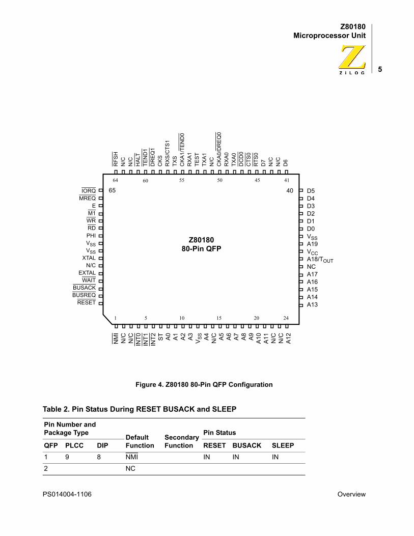
Figure 4. Z80180 80-Pin QFP Configuration
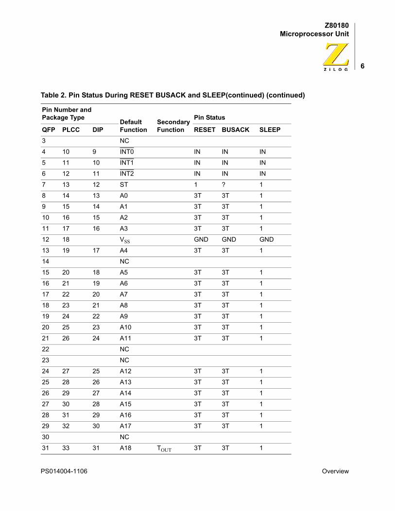
Table 2. Pin Status During RESET BUSACK and SLEEP
Pin Number and Package Type
Default Function
Secondary Function
Pin Status
QFP PLCC DIP RESET BUSACK SLEEP1 9 8 NMI IN IN IN
2 NC
4065IORQMREQ
EM1
WRRDPHIVSSVSS
XTALN/C
EXTALWAIT
BUSACKBUSREQ
RESET
NM
IN
/CN
/CIN
T0IN
T1IN
T2 ST A0
A1
A2
A3
VS
SA
4N
/C A5
A6
A7
A8
A9
A10
A11
N/C
N/C
A12
RFS
HN
/CN
/CH
ALT
TEN
D1
DR
EQ
1C
KS
RX
S/C
TS1
TXS
CK
A1/
TEN
D0
RX
A1TE
ST
TXA
1N
/CC
KA
0/D
RE
Q0
RX
A0TX
A0
DC
D0
CTS
0R
TS0
D7
N/C
N/C
D6
5 10 15 20 24
60 55 50 45 4164
Z8018080-Pin QFP
1
D5D4D3D2D1D0VSSA19VCCA18/TOUTNCA17A16A15A14A13
PS014004-1106 Overview
Z80180Microprocessor Unit
6
3 NC
4 10 9 INT0 IN IN IN
5 11 10 INT1 IN IN IN
6 12 11 INT2 IN IN IN
7 13 12 ST 1 ? 1
8 14 13 A0 3T 3T 1
9 15 14 A1 3T 3T 1
10 16 15 A2 3T 3T 1
11 17 16 A3 3T 3T 1
12 18 VSS GND GND GND
13 19 17 A4 3T 3T 1
14 NC
15 20 18 A5 3T 3T 1
16 21 19 A6 3T 3T 1
17 22 20 A7 3T 3T 1
18 23 21 A8 3T 3T 1
19 24 22 A9 3T 3T 1
20 25 23 A10 3T 3T 1
21 26 24 A11 3T 3T 1
22 NC
23 NC
24 27 25 A12 3T 3T 1
25 28 26 A13 3T 3T 1
26 29 27 A14 3T 3T 1
27 30 28 A15 3T 3T 1
28 31 29 A16 3T 3T 1
29 32 30 A17 3T 3T 1
30 NC
31 33 31 A18 TOUT 3T 3T 1
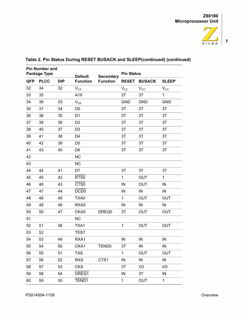
Table 2. Pin Status During RESET BUSACK and SLEEP(continued) (continued)
Pin Number and Package Type
Default Function
Secondary Function
Pin Status
QFP PLCC DIP RESET BUSACK SLEEP
PS014004-1106 Overview
Z80180Microprocessor Unit
7
32 34 32 VCC VCC VCC VCC
33 35 A19 3T 3T 1
34 36 33 VSS GND GND GND
35 37 34 D0 3T 3T 3T
36 38 35 D1 3T 3T 3T
37 39 36 D2 3T 3T 3T
38 40 37 D3 3T 3T 3T
39 41 38 D4 3T 3T 3T
40 42 39 D5 3T 3T 3T
41 43 40 D6 3T 3T 3T
42 NC
43 NC
44 44 41 D7 3T 3T 3T
45 45 42 RTS0 1 OUT 1
46 46 43 CTS0 IN OUT IN
47 47 44 DCD0 IN IN IN
48 48 45 TXA0 1 OUT OUT
49 49 46 RXA0 IN IN IN
50 50 47 CKA0 DREQ0 3T OUT OUT
51 NC
52 51 48 TXA1 1 OUT OUT
53 52 TEST
54 53 49 RXA1 IN IN IN
55 54 50 CKA1 TEND0 3T IN IN
56 55 51 TXS 1 OUT OUT
57 56 52 RXS CTS1 IN IN IN
58 57 53 CKS 3T I/O I/O
59 58 54 DREQ1 IN 3T IN
60 59 55 TEND1 1 OUT 1
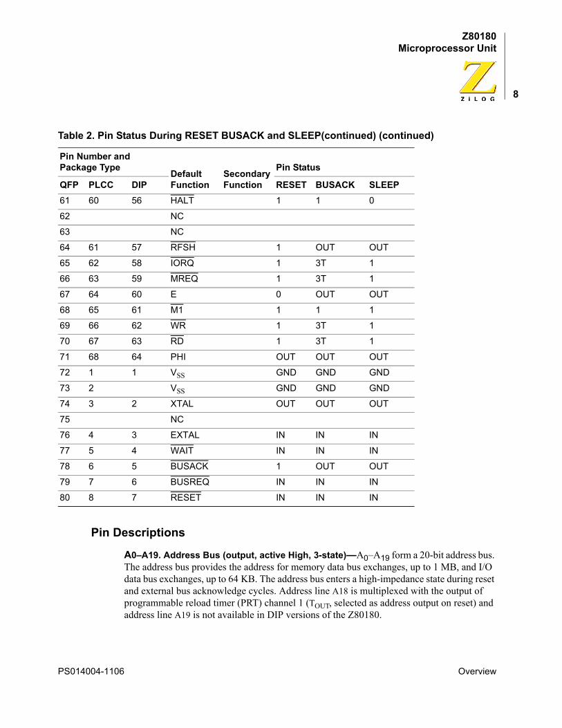
Table 2. Pin Status During RESET BUSACK and SLEEP(continued) (continued)
Pin Number and Package Type
Default Function
Secondary Function
Pin Status
QFP PLCC DIP RESET BUSACK SLEEP
PS014004-1106 Overview
Z80180Microprocessor Unit
8
Pin Descriptions
A0–A19. Address Bus (output, active High, 3-state)—A0–A19 form a 20-bit address bus. The address bus provides the address for memory data bus exchanges, up to 1 MB, and I/O data bus exchanges, up to 64 KB. The address bus enters a high-impedance state during reset and external bus acknowledge cycles. Address line A18 is multiplexed with the output of programmable reload timer (PRT) channel 1 (TOUT, selected as address output on reset) and address line A19 is not available in DIP versions of the Z80180.
61 60 56 HALT 1 1 0
62 NC
63 NC
64 61 57 RFSH 1 OUT OUT
65 62 58 IORQ 1 3T 1
66 63 59 MREQ 1 3T 1
67 64 60 E 0 OUT OUT
68 65 61 M1 1 1 1
69 66 62 WR 1 3T 1
70 67 63 RD 1 3T 1
71 68 64 PHI OUT OUT OUT
72 1 1 VSS GND GND GND
73 2 VSS GND GND GND
74 3 2 XTAL OUT OUT OUT
75 NC
76 4 3 EXTAL IN IN IN
77 5 4 WAIT IN IN IN
78 6 5 BUSACK 1 OUT OUT
79 7 6 BUSREQ IN IN IN
80 8 7 RESET IN IN IN
Table 2. Pin Status During RESET BUSACK and SLEEP(continued) (continued)
Pin Number and Package Type
Default Function
Secondary Function
Pin Status
QFP PLCC DIP RESET BUSACK SLEEP
PS014004-1106 Overview
Z80180Microprocessor Unit
9
BUSACK—Bus Acknowledge (output, active Low). BUSACK indicates the requesting device, the MPU address and data bus, and some control signals that enter their high-imped-ance state.BUSREQ—Bus Request (input, active Low). This input is used by external devices (such as DMA controllers) to request access to the system bus. This request demands a higher priority than NMI and is always recognized at the end of the current machine cycle. This signal stops the CPU from executing further instruc-tions and places address and data buses, and other control signals, into the high-impedance state.CKA0, CKA1—Asynchronous Clock 0 and 1 (bidirectional, active High). When in output mode, these pins are the transmit and receive clock outputs from the ASCI baud rate generators. When in input mode, these pins serve as the external clock inputs for the ASCI baud rate generators. CKA0 is multiplexed with DREQ0, and CKA1 is multiplexed with TEND0.CKS—Serial Clock (bidirectional, active High). This line is the clock for the CSIO channel.CLOCK—System Clock (output, active High). The output is used as a reference clock for the MPU and the external system. The frequency of this output is equal to one-half that of the crystal or input clock frequency.CTS0–CTS1—Clear to send 0 and 1 (inputs, active Low). These lines are modem control signals for the ASCI channels. CTS1 is multiplexed with RXS.D0–D7—Data Bus (bidirectional, active High, 3-state). D0–D7 constitute an 8-bit bidirectional data bus, used for the transfer of information to and from I/O and memory devices. The data bus enters the high-impedance state during reset and external bus acknowledge cycles.DCD0—Data Carrier Detect 0 (input, active Low). A programmable modem control signal for ASCI channel 0.
DREQ0, DREQ1. DMA Request 0 and 1 (input, active Low). DREQ is used to request a DMA transfer from one of the on-chip DMA channels. The DMA channels monitor these inputs to determine when an external device is ready for a READ or WRITE operation. These inputs can be programmed to be either level or edge sensed. DREQ0 is multiplexed with CKA0.E—Enable Clock (output, active High). Synchronous machine cycle clock output during bus transactions.EXTAL—External Clock Crystal (input, active High). Crystal oscillator connections. An external clock can be input to the Z80180 on this pin when a crystal is not used. This input is Schmitt-triggered.HALT—HALT/SLEEP (output, active Low). This output is asserted after the CPU executes either the HALT or SLEEP instruction, and is waiting for either nonmaskable or maskable
PS014004-1106 Overview
Z80180Microprocessor Unit
10
interrupt before operation resumes. It is also used with the M1 and ST signals to decode status of the CPU machine cycle.INT0—Maskable Interrupt Request 0 (input, active Low). This signal is generated by exter-nal I/O devices. The CPU honors these requests at the end of the current instruction cycle as long as the NMI and BUSREQ signals are inactive. The CPU acknowledges this interrupt request with an interrupt acknowledge cycle. During this cycle, both the M1 and IORQ signals become active.INT1, INT2—Maskable Interrupt Request 1 and 2 (inputs, active Low). This signal is gener-ated by external I/O devices. The CPU honors these requests at the end of the current instruction cycle as long as the NMI, BUSREQ, and INT0 signals are inactive. The CPU acknowledges these requests with an interrupt acknowledge cycle. Unlike the acknowledg-ment for INT0, during this cycle neither the M1 or IORQ signals become active.IORQ—I/O Request (output, active Low, 3-state). IORQ indicates that the address bus con-tains a valid I/O address for an I/O READ or I/O WRITE operation. IORQ is also generated, along with M1, during the acknowledgment of the INT0 input signal to indicate that an inter-rupt response vector can be placed onto the data bus. This signal is analogous to the IOE sig-nal of the Z64180.M1—Machine Cycle 1 (output, active Low). Together with MREQ, M1 indicates that the cur-rent cycle is the opcode fetch cycle of and instruction execution. Together with IORQ, M1 indicates that the current cycle is for an interrupt acknowledge. It is also used with the HALT and ST signal to decode status of the CPU machine cycle. This signal is analogous to the LIR signal of the Z64180.MREQ—Memory Request (output, active Low, 3-state). MREQ indicates that the address bus holds a valid address for a memory READ or memory WRITE operation. This signal is analogous to the ME signal of Z64180.NMI—Nonmaskable Interrupt (input, negative edge triggered). NMI demands a higher prior-ity than INT and is always recognized at the end of an instruction, regardless of the state of the interrupt enable flip-flops. This signal forces CPU execution to continue at location 0066h.RD—Opcode Reinitialized (output, active Low, 3-state). RD indicated that the CPU wants to read data from memory or an I/O device. The addressed I/O or memory device must use this signal to gate data onto the CPU data bus.RFSH—Refresh (output, active Low). Together with MREQ, RFSH indicates that the current CPU machine cycle and the contents of the address bus must be used for refresh of dynamic memories. The low order 8 bits of the address bus (A7–A10) contain the refresh address. This signal is analogous to the REF signal of the Z64180.RTS0—Request to Send 0 (output, active Low). A programmable modem control signal for ASCI channel 0.RXA0, RXA1—Receive Data 0 and 1 (input, active High). These signals are the receive data to the ASCI channels.
PS014004-1106 Overview
Z80180Microprocessor Unit
11
RXS—Clocked Serial Receive Data (input, active High). This line is the receiver data for the CSIO channel. RXS is multiplexed with the CTS1 signal for ASCI channel 1.ST—Status (output, active High). This signal is used with the M1 and HALT output to decode the status of the CPU machine cycle.
TEND0, TEND1—Transfer End 0 and 1 (outputs, active Low). This output is asserted active during the most recent WRITE cycle of a DMA operation. It is used to indicate the end of the block transfer. TEND0 is multiplexed with CKA1.TEST—Test (output, not in DIP version). This pin is for test and must be left open.TOUT—Timer Out (output, active High). TOUT is the pulse output from PRT channel 1. This line is multiplexed with A18 of the address bus.TXA0, TXA1—Transmit Data 0 and 1 (outputs, active High). These signals are the transmit-ted data from the ASCI channels. Transmitted data changes are with respect to the falling edge of the transmit clock.TXS—Clocked Serial Transmit Data (output, active High). This line is the transmitted data from the CSIO channel.WAIT—Wait (input, active Low). WAIT indicated to the MPU that the addressed memory or I/O devices are not ready for a data transfer. This input is sampled on the falling edge of T2 (and subsequent wait states). If the input is sampled Low, then the additional wait states are inserted until the WAIT input is sampled high, at which time execution continues.WR—WRITE (output, active Low, 3-state). WR indicated that the CPU data bus holds valid data to be stored at the addressed I/O or memory location.XTAL—Crystal (input, active High). Crystal oscillator connection. This pin must be left open if an external clock is used instead of a crystal. The oscillator input is not a TTL level
Table 3. Status Summary
ST HALT M1 Operation0 1 0 CPU Operation (1st opcode fetch)1 1 0 CPU Operation (2nd opcode and 3rd opcode
fetch)1 1 1 CPU Operation (MC except for opcode fetch)0 X 1 DMA Operation0 0 0 HALT Mode1 0 1 SLEEP Mode (including SYSTEM STOP
Mode)Notes:X = Reserved.MC = Machine Cycle.
PS014004-1106 Overview
Z80180Microprocessor Unit
12
(see DC Characteristics on page 21). Several pins are used for different conditions, depending on the circumstance.
Multiplexed Pin Descriptions
Table 4. Multiplexed Pin Descriptions
Pin Description
A18/TOUT During RESET, this pin is initialized as A18 pin. If either TOC1 or TOC0 bit of the Timer Control Register (TCR) is set to 1, TOUT function is selected. If TOC1 and TOC0 are cleared to 0, A18 function is selected.
CKA0/DREQ0 During RESET, this pin is initialized as CKA0 pin. If either DM1 or SM1 in DMA Mode Register (DMODE) is set to 1, DREQ0 function is always selected.
CKA1/TEND0 During RESET, this pin is initialized as CKA1 pin. If CKA1D bit in ASCI control register ch1 (CNTLA1) is set to 1, TEND0 function is selected. If CKA1D bit is set to 0, CKA1 function is selected.
RXS/CTS1 During RESET, this pin is initialized as RXS pin. If CTS1E bit in ASCI status register ch1 (STAT1) is set to 1, CTS1 function is selected. If CTS1E bit is set to 0, RXS function is selected.
PS014004-1106 Overview
Z80180Microprocessor Unit
13
ArchitectureThe Z180® combines a high-performance CPU core with a variety of system and I/O resources useful in a broad range of applications. The CPU core consists of five functional blocks: clock generator, bus state controller, interrupt controller, memory management unit (MMU), and the central processing unit (CPU). The integrated I/O resources make up the remaining four function blocks: direct memory access (DMA) control (2 channels), asynchronous serial communication interface (ASCI) 2 channels, programma-ble reload timers (PRT) 2 channels, and a clock serial I/O (CSIO) channel.Clock Generator—Generates system clock from an external crystal or clock input. The external clock is divided by two or one and provided to both internal and external devices. Bus State Controller—This logic performs all of the status and bus control activity associated with both the CPU and some on-chip peripherals. Included are wait-state timing, reset cycles, DRAM refresh, and DMA bus exchanges.Interrupt Controller—This logic monitors and prioritizes the variety of internal and external interrupts and traps to provide the correct responses from the CPU. To maintain compatibility with the Z80® CPU, three different interrupts modes are supported.Memory Management Unit—The MMU allows you to map the memory used by the CPU (logically only 64 KB) into the 1-MB addressing range supported by the Z80180. The orga-nization of the MMU object code allows maintenance compatibility with the Z80 CPU, while offering access to an extended memory space. This organization is achieved by using an effective common area-banked area scheme.Central Processing Unit—The CPU is microcoded to provide a core that is object-code compatible with the Z80 CPU. It also provides a superset of the Z80 instruction set, includ-ing 8-bit multiply. The core is modified to allow many of the instructions to execute in fewer clock cycles.DMA Controller—The DMA controller provides high speed transfers between memory and I/O devices. Transfer operations supported are memory-to-memory, memory to/from I/O, and I/O-to-I/O. Transfer modes supported are request, burst, and cycle steal. DMA transfers can access the full 1 MB address range with a block length up to 64 KB, and can cross over 64K boundaries. Asynchronous Serial Communication Interface (ASC)—The ASCI logic provides two individual full-duplex UARTs. Each channel includes a programmable baud rate generator and modem control signals. The ASCI channels also support a multiprocessor communication format as well as break detection and generation.Programmable Reload Timers (PRT)—This logic consists of two separate channels, each containing a 16-bit counter (timer) and count reload register. The time base for the counters is derived from the system clock (divided by 20) before reaching the counter. PRT channel 1 provides an optional output to allow for waveform generation.
PS014004-1106 Architecture
Z80180Microprocessor Unit
14
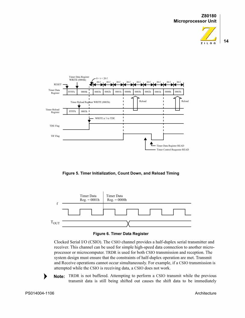
Figure 5. Timer Initialization, Count Down, and Reload Timing
Figure 6. Timer Data Register
Clocked Serial I/O (CSIO). The CSIO channel provides a half-duplex serial transmitter and receiver. This channel can be used for simple high-speed data connection to another micro-processor or microcomputer. TRDR is used for both CSIO transmission and reception. The system design must ensure that the constraints of half-duplex operation are met. Transmit and Receive operations cannot occur simultaneously. For example, if a CSIO transmission is attempted while the CSIO is receiving data, a CSIO does not work.
TRDR is not buffered. Attempting to perform a CSIO transmit while the previoustransmit data is still being shifted out causes the shift data to be immediately
FFFFh 0004h 0003h 0002h 0001h 0000h 0003h 0002h 0001h 0000h 0003h
Timer Data RegisterWRITE (0004h)
Timer DataRegister
Timer ReloadRegister
TDE Flag
TIF Flag
RESET20 f 20 f 20 f 20 f 20 f 20 f 20 f 20 f 20 f0 < t < 20 f
Timer Reload Register WRITE (0003h)
FFFFh 0003h
Reload Reload
WRITE a 1 to TDE
Timer Data Register READTimer Control Requestor READ
Timer DataReg. = 0001h
Timer Data Reg. = 0000h
TOUT
f
Note:
PS014004-1106 Architecture
Z80180Microprocessor Unit
15
updated, corrupting the transmit operation in progress. Reading TRDR while atransmit or receive is in progress must be avoided.
Figure 7. CSIO Block Diagram
Operation Modes
Z80® versus 64180 Compatibility
The Z80180 is descended from two different ancestor processors, ZiLOG's original Z80 and the Hitachi 64180. The Operating Mode Control Register (OMCR), illustrated in Figure 8, can be programmed to select between certain Z80 and 64180 differences.
.
Figure 8. Operating Control Register (OMCR: I/O Address = 3Eh)
M1E (M1 Enable)—This bit controls the M1 output and is set to a 1 during RESET.
When M1E = 1, the M1 output is asserted Low during the opcode fetch cycle, the INT0 acknowledge cycle, and the first machine cycle of the NMI acknowledge.
Internal Address/Data Bus
CSIO Transmit/ReceiveData Register:TRDR (8)
CSIO Control Register:CNTR (8)
Baud RateGeneratorTXS
RXS
CKS
φ
Interrupt Request
D7
Reserved
D6 D5 —
IOC (R/W)
M1TE (W)
M1E (R/W)
— — — —
PS014004-1106 Architecture
Z80180Microprocessor Unit
16
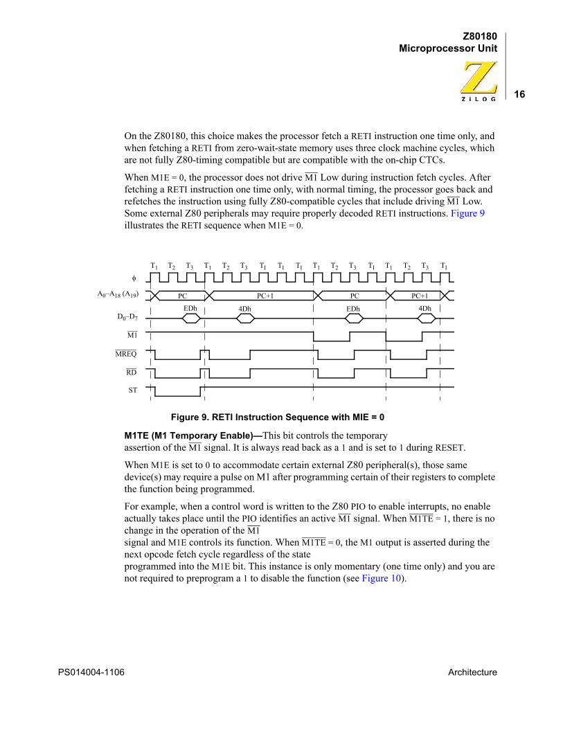
On the Z80180, this choice makes the processor fetch a RETI instruction one time only, and when fetching a RETI from zero-wait-state memory uses three clock machine cycles, which are not fully Z80-timing compatible but are compatible with the on-chip CTCs.
When M1E = 0, the processor does not drive M1 Low during instruction fetch cycles. After fetching a RETI instruction one time only, with normal timing, the processor goes back and refetches the instruction using fully Z80-compatible cycles that include driving M1 Low. Some external Z80 peripherals may require properly decoded RETI instructions. Figure 9 illustrates the RETI sequence when M1E = 0.
Figure 9. RETI Instruction Sequence with MIE = 0
M1TE (M1 Temporary Enable)—This bit controls the temporary assertion of the M1 signal. It is always read back as a 1 and is set to 1 during RESET.
When M1E is set to 0 to accommodate certain external Z80 peripheral(s), those same device(s) may require a pulse on M1 after programming certain of their registers to complete the function being programmed.
For example, when a control word is written to the Z80 PIO to enable interrupts, no enable actually takes place until the PIO identifies an active M1 signal. When M1TE = 1, there is no change in the operation of the M1 signal and M1E controls its function. When M1TE = 0, the M1 output is asserted during the next opcode fetch cycle regardless of the state programmed into the M1E bit. This instance is only momentary (one time only) and you are not required to preprogram a 1 to disable the function (see Figure 10).
T1 T2 T3 T1 T2 T3 TI TI TI T1 T2 T3 T1 T2 T3TI TI
A0–A18 (A19)
φ
D0–D7
PC PC+1 PC PC+1
EDh 4Dh EDh 4Dh
MREQ
M1
RD
ST
PS014004-1106 Architecture
Z80180Microprocessor Unit
17
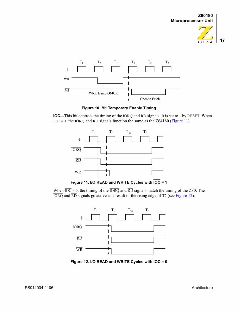
Figure 10. M1 Temporary Enable Timing
IOC—This bit controls the timing of the IORQ and RD signals. It is set to 1 by RESET. When IOC = 1, the IORQ and RD signals function the same as the Z64180 (Figure 11).
Figure 11. I/O READ and WRITE Cycles with IOC = 1
When IOC = 0, the timing of the IORQ and RD signals match the timing of the Z80. The IORQ and RD signals go active as a result of the rising edge of T2 (see Figure 12).
Figure 12. I/O READ and WRITE Cycles with IOC = 0
T1 T2 T3 T1 T2 T3
f
WR
M1
Opcode FetchWRITE into OMCR
T1 T2 TW T3
φ
IORQ
RD
WR
T1 T2 TW T3
φ
IORQ
RD
WR
PS014004-1106 Architecture
Z80180Microprocessor Unit
18
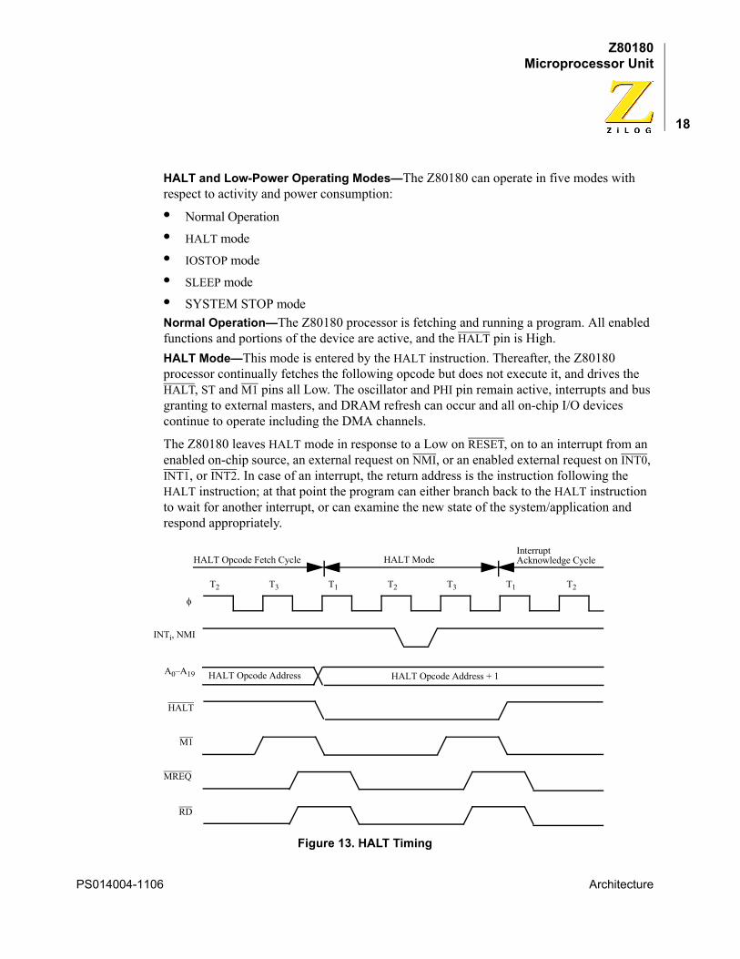
HALT and Low-Power Operating Modes—The Z80180 can operate in five modes with respect to activity and power consumption:
• Normal Operation• HALT mode• IOSTOP mode• SLEEP mode• SYSTEM STOP modeNormal Operation—The Z80180 processor is fetching and running a program. All enabled functions and portions of the device are active, and the HALT pin is High.HALT Mode—This mode is entered by the HALT instruction. Thereafter, the Z80180 processor continually fetches the following opcode but does not execute it, and drives the HALT, ST and M1 pins all Low. The oscillator and PHI pin remain active, interrupts and bus granting to external masters, and DRAM refresh can occur and all on-chip I/O devices continue to operate including the DMA channels.
The Z80180 leaves HALT mode in response to a Low on RESET, on to an interrupt from an enabled on-chip source, an external request on NMI, or an enabled external request on INT0, INT1, or INT2. In case of an interrupt, the return address is the instruction following the HALT instruction; at that point the program can either branch back to the HALT instruction to wait for another interrupt, or can examine the new state of the system/application and respond appropriately.
Figure 13. HALT Timing
HALT Opcode Fetch Cycle HALT Mode
φ
T2 T3 T1 T2 T3 T1 T2
INTi, NMI
A0–A19
HALT
M1
MREQ
RD
InterruptAcknowledge Cycle
HALT Opcode Address HALT Opcode Address + 1
PS014004-1106 Architecture
Z80180Microprocessor Unit
19
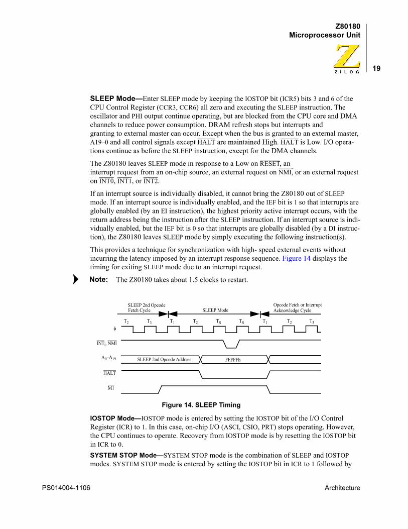
SLEEP Mode—Enter SLEEP mode by keeping the IOSTOP bit (ICR5) bits 3 and 6 of the CPU Control Register (CCR3, CCR6) all zero and executing the SLEEP instruction. The oscillator and PHI output continue operating, but are blocked from the CPU core and DMA channels to reduce power consumption. DRAM refresh stops but interrupts and granting to external master can occur. Except when the bus is granted to an external master, A19–0 and all control signals except HALT are maintained High. HALT is Low. I/O opera-tions continue as before the SLEEP instruction, except for the DMA channels.
The Z80180 leaves SLEEP mode in response to a Low on RESET, an interrupt request from an on-chip source, an external request on NMI, or an external request on INT0, INT1, or INT2.
If an interrupt source is individually disabled, it cannot bring the Z80180 out of SLEEP mode. If an interrupt source is individually enabled, and the IEF bit is 1 so that interrupts are globally enabled (by an EI instruction), the highest priority active interrupt occurs, with the return address being the instruction after the SLEEP instruction. If an interrupt source is indi-vidually enabled, but the IEF bit is 0 so that interrupts are globally disabled (by a DI instruc-tion), the Z80180 leaves SLEEP mode by simply executing the following instruction(s).
This provides a technique for synchronization with high- speed external events without incurring the latency imposed by an interrupt response sequence. Figure 14 displays the timing for exiting SLEEP mode due to an interrupt request.
The Z80180 takes about 1.5 clocks to restart.
Figure 14. SLEEP Timing
IOSTOP Mode—IOSTOP mode is entered by setting the IOSTOP bit of the I/O Control Register (ICR) to 1. In this case, on-chip I/O (ASCI, CSIO, PRT) stops operating. However, the CPU continues to operate. Recovery from IOSTOP mode is by resetting the IOSTOP bit in ICR to 0.SYSTEM STOP Mode—SYSTEM STOP mode is the combination of SLEEP and IOSTOP modes. SYSTEM STOP mode is entered by setting the IOSTOP bit in ICR to 1 followed by
Note:
SLEEP 2nd OpcodeSLEEP Mode
φT2 T3 T1 T2 TS TS T1
INTi, NMI
A0–A19
HALT
M1
Opcode Fetch or InterruptAcknowledge Cycle
SLEEP 2nd Opcode Address FFFFFh
Fetch Cycle
T2 T3
PS014004-1106 Architecture
Z80180Microprocessor Unit
20
execution of the SLEEP instruction. In this mode, on-chip I/O and CPU stop operating, reducing power consumption, but the PHI output continues to operate. Recovery from SYS-TEM STOP mode is the same as recovery from SLEEP mode except that internal I/O sources (disabled by IOSTOP) cannot generate a recovery interrupt.
Standard Test Conditions
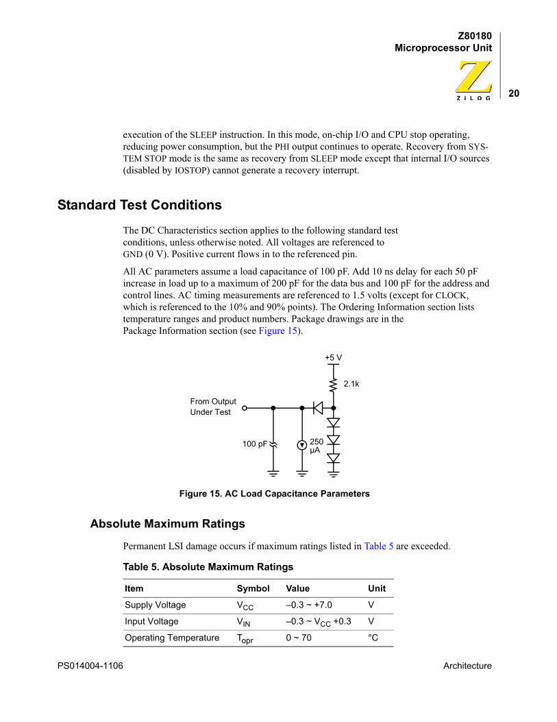
The DC Characteristics section applies to the following standard test conditions, unless otherwise noted. All voltages are referenced to GND (0 V). Positive current flows in to the referenced pin.
All AC parameters assume a load capacitance of 100 pF. Add 10 ns delay for each 50 pF increase in load up to a maximum of 200 pF for the data bus and 100 pF for the address and control lines. AC timing measurements are referenced to 1.5 volts (except for CLOCK, which is referenced to the 10% and 90% points). The Ordering Information section lists temperature ranges and product numbers. Package drawings are in the Package Information section (see Figure 15).
Figure 15. AC Load Capacitance Parameters
Absolute Maximum Ratings
Permanent LSI damage occurs if maximum ratings listed in Table 5 are exceeded.
Table 5. Absolute Maximum Ratings
Item Symbol Value Unit
Supply Voltage VCC –0.3 ~ +7.0 V
Input Voltage VIN –0.3 ~ VCC +0.3 V
Operating Temperature Topr 0 ~ 70 °C
+5 V
From Output
100 pF
Under Test
250µA
2.1k
PS014004-1106 Architecture
Z80180Microprocessor Unit
21
Normal operation must be under recommended operating conditions. If theseconditions are exceeded, it affects reliability of LSI.
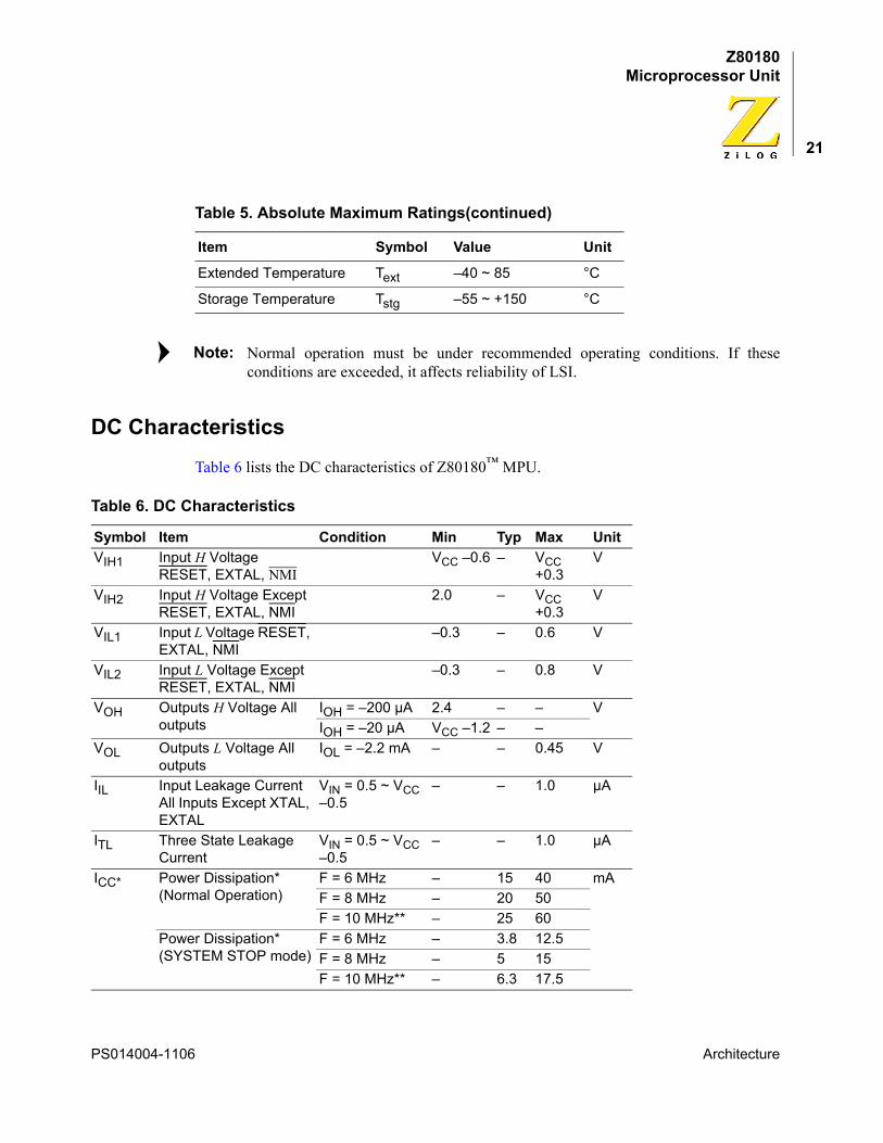
DC Characteristics
Table 6 lists the DC characteristics of Z80180™ MPU.
Extended Temperature Text –40 ~ 85 °C
Storage Temperature Tstg –55 ~ +150 °C
Table 6. DC Characteristics
Symbol Item Condition Min Typ Max UnitVIH1 Input H Voltage
RESET, EXTAL, NMIVCC –0.6 – VCC
+0.3V
VIH2 Input H Voltage Except RESET, EXTAL, NMI
2.0 – VCC +0.3
V
VIL1 Input L Voltage RESET, EXTAL, NMI
–0.3 – 0.6 V
VIL2 Input L Voltage Except RESET, EXTAL, NMI
–0.3 – 0.8 V
VOH Outputs H Voltage All outputs
IOH = –200 µA 2.4 – – VIOH = –20 µA VCC –1.2 – –
VOL Outputs L Voltage All outputs
IOL = –2.2 mA – – 0.45 V
IIL Input Leakage Current All Inputs Except XTAL, EXTAL
VIN = 0.5 ~ VCC –0.5
– – 1.0 µA
ITL Three State Leakage Current
VIN = 0.5 ~ VCC –0.5
– – 1.0 µA
ICC* Power Dissipation* (Normal Operation)
F = 6 MHz – 15 40 mAF = 8 MHz – 20 50F = 10 MHz** – 25 60
Power Dissipation* (SYSTEM STOP mode)
F = 6 MHz – 3.8 12.5F = 8 MHz – 5 15F = 10 MHz** – 6.3 17.5
Table 5. Absolute Maximum Ratings(continued)
Item Symbol Value Unit
Note:
PS014004-1106 Architecture
Z80180Microprocessor Unit
22
AC Characteristics
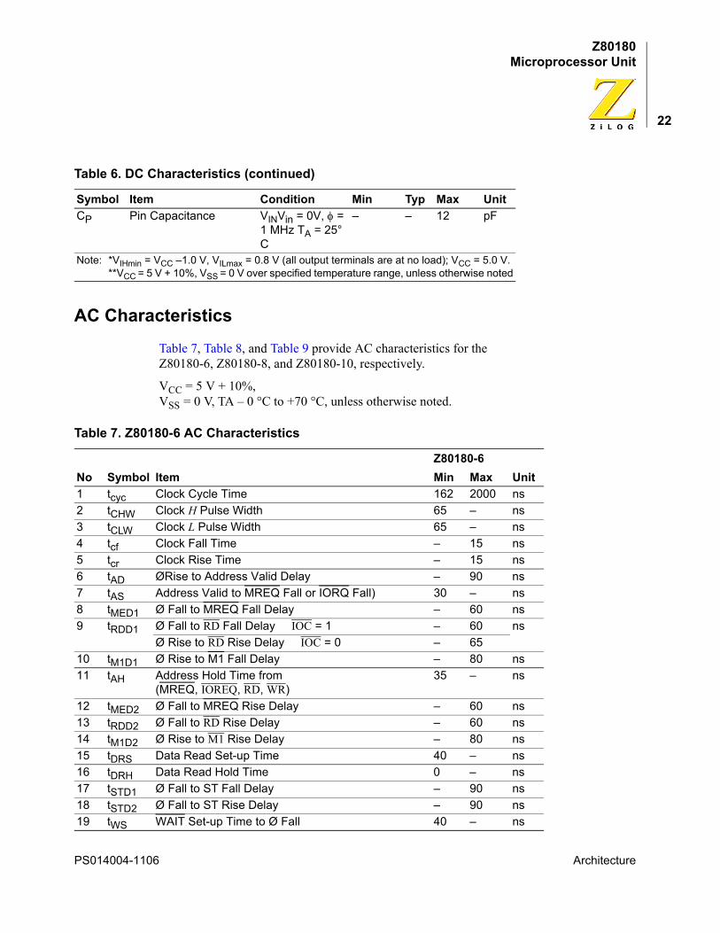
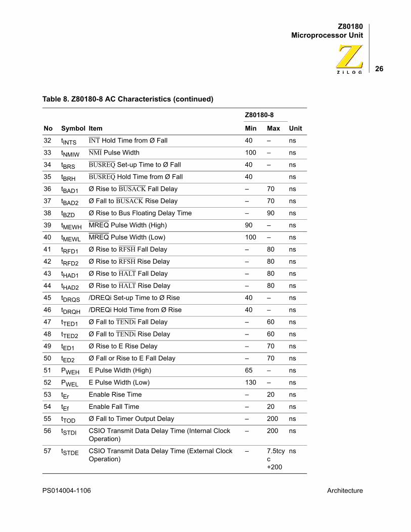
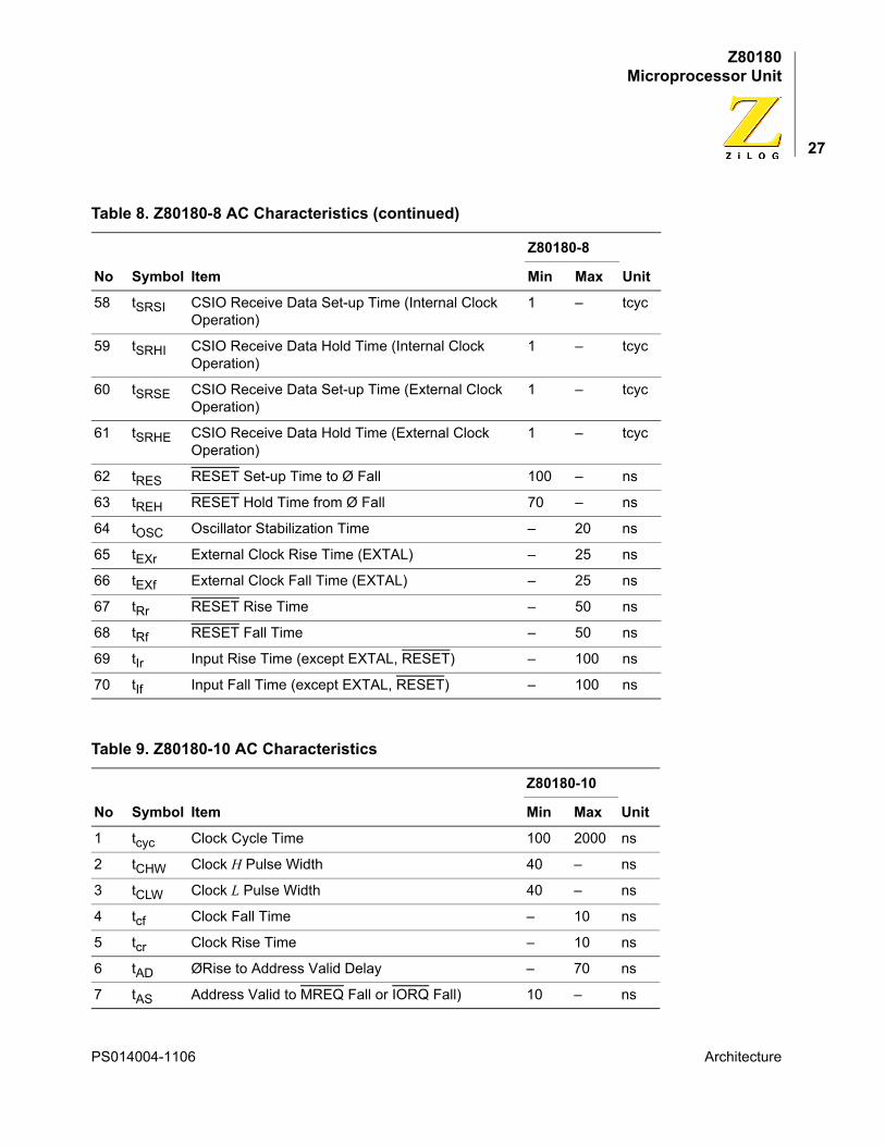
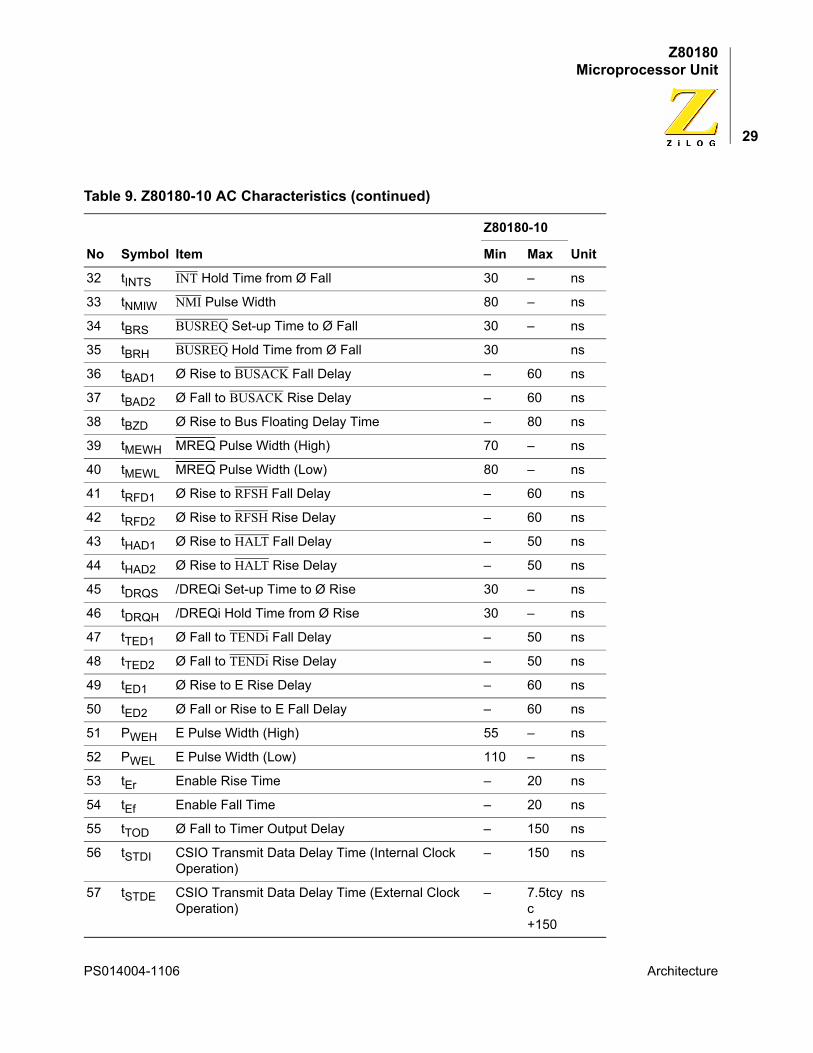
Table 7, Table 8, and Table 9 provide AC characteristics for the Z80180-6, Z80180-8, and Z80180-10, respectively.
VCC = 5 V + 10%, VSS = 0 V, TA – 0 °C to +70 °C, unless otherwise noted.
CP Pin Capacitance VINVin = 0V, φ = 1 MHz TA = 25° C
– – 12 pF
Note: *VIHmin = VCC –1.0 V, VILmax = 0.8 V (all output terminals are at no load); VCC = 5.0 V. **VCC = 5 V + 10%, VSS = 0 V over specified temperature range, unless otherwise noted
Table 7. Z80180-6 AC Characteristics
No Symbol ItemZ80180-6
UnitMin Max1 tcyc Clock Cycle Time 162 2000 ns2 tCHW Clock H Pulse Width 65 – ns3 tCLW Clock L Pulse Width 65 – ns4 tcf Clock Fall Time – 15 ns5 tcr Clock Rise Time – 15 ns6 tAD ØRise to Address Valid Delay – 90 ns7 tAS Address Valid to MREQ Fall or IORQ Fall) 30 – ns8 tMED1 Ø Fall to MREQ Fall Delay – 60 ns9 tRDD1 Ø Fall to RD Fall Delay IOC = 1 – 60 ns
Ø Rise to RD Rise Delay IOC = 0 – 6510 tM1D1 Ø Rise to M1 Fall Delay – 80 ns11 tAH Address Hold Time from
(MREQ, IOREQ, RD, WR)35 – ns
12 tMED2 Ø Fall to MREQ Rise Delay – 60 ns13 tRDD2 Ø Fall to RD Rise Delay – 60 ns14 tM1D2 Ø Rise to M1 Rise Delay – 80 ns15 tDRS Data Read Set-up Time 40 – ns16 tDRH Data Read Hold Time 0 – ns17 tSTD1 Ø Fall to ST Fall Delay – 90 ns18 tSTD2 Ø Fall to ST Rise Delay – 90 ns19 tWS WAIT Set-up Time to Ø Fall 40 – ns
Table 6. DC Characteristics (continued)
Symbol Item Condition Min Typ Max Unit
PS014004-1106 Architecture
Z80180Microprocessor Unit
23
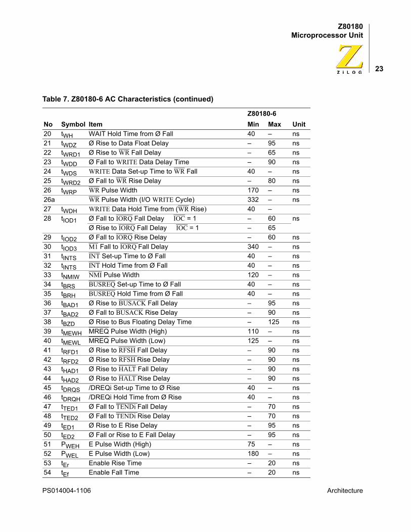
20 tWH WAIT Hold Time from Ø Fall 40 – ns21 tWDZ Ø Rise to Data Float Delay – 95 ns22 tWRD1 Ø Rise to WR Fall Delay – 65 ns23 tWDD Ø Fall to WRITE Data Delay Time – 90 ns24 tWDS WRITE Data Set-up Time to WR Fall 40 – ns25 tWRD2 Ø Fall to WR Rise Delay – 80 ns26 tWRP WR Pulse Width 170 – ns26a WR Pulse Width (I/O WRITE Cycle) 332 – ns27 tWDH WRITE Data Hold Time from (WR Rise) 40 –28 tIOD1 Ø Fall to IORQ Fall Delay IOC = 1 – 60 ns
Ø Rise to IORQ Fall Delay IOC = 1 – 6529 tIOD2 Ø Fall to IORQ Rise Delay – 60 ns30 tIOD3 M1 Fall to IORQ Fall Delay 340 – ns31 tINTS INT Set-up Time to Ø Fall 40 – ns32 tINTS INT Hold Time from Ø Fall 40 – ns33 tNMIW NMI Pulse Width 120 – ns34 tBRS BUSREQ Set-up Time to Ø Fall 40 – ns35 tBRH BUSREQ Hold Time from Ø Fall 40 – ns36 tBAD1 Ø Rise to BUSACK Fall Delay – 95 ns37 tBAD2 Ø Fall to BUSACK Rise Delay – 90 ns38 tBZD Ø Rise to Bus Floating Delay Time – 125 ns39 tMEWH MREQ Pulse Width (High) 110 – ns40 tMEWL MREQ Pulse Width (Low) 125 – ns41 tRFD1 Ø Rise to RFSH Fall Delay – 90 ns42 tRFD2 Ø Rise to RFSH Rise Delay – 90 ns43 tHAD1 Ø Rise to HALT Fall Delay – 90 ns44 tHAD2 Ø Rise to HALT Rise Delay – 90 ns45 tDRQS /DREQi Set-up Time to Ø Rise 40 – ns46 tDRQH /DREQi Hold Time from Ø Rise 40 – ns47 tTED1 Ø Fall to TENDi Fall Delay – 70 ns48 tTED2 Ø Fall to TENDi Rise Delay – 70 ns49 tED1 Ø Rise to E Rise Delay – 95 ns50 tED2 Ø Fall or Rise to E Fall Delay – 95 ns51 PWEH E Pulse Width (High) 75 – ns52 PWEL E Pulse Width (Low) 180 – ns53 tEr Enable Rise Time – 20 ns54 tEf Enable Fall Time – 20 ns
Table 7. Z80180-6 AC Characteristics (continued)
No Symbol ItemZ80180-6
UnitMin Max
PS014004-1106 Architecture
Z80180Microprocessor Unit
24
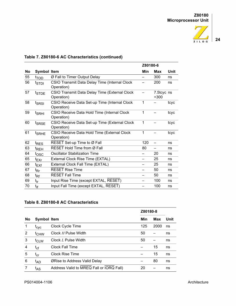
55 tTOD Ø Fall to Timer Output Delay – 300 ns56 tSTDI CSIO Transmit Data Delay Time (Internal Clock
Operation)– 200 ns
57 tSTDE CSIO Transmit Data Delay Time (External Clock Operation)
– 7.5tcyc+300
ns
58 tSRSI CSIO Receive Data Set-up Time (Internal Clock Operation)
1 – tcyc
59 tSRHI CSIO Receive Data Hold Time (Internal Clock Operation)
1 – tcyc
60 tSRSE CSIO Receive Data Set-up Time (External Clock Operation)
1 – tcyc
61 tSRHE CSIO Receive Data Hold Time (External Clock Operation)
1 – tcyc
62 tRES RESET Set-up Time to Ø Fall 120 – ns63 tREH RESET Hold Time from Ø Fall 80 – ns64 tOSC Oscillator Stabilization Time – 20 ns65 tEXr External Clock Rise Time (EXTAL) – 25 ns66 tEXf External Clock Fall Time (EXTAL) – 25 ns67 tRr RESET Rise Time – 50 ns68 tRf RESET Fall Time – 50 ns69 tIr Input Rise Time (except EXTAL, RESET) – 100 ns70 tIf Input Fall Time (except EXTAL, RESET) – 100 ns
Table 8. Z80180-8 AC Characteristics
No Symbol Item
Z80180-8
UnitMin Max
1 tcyc Clock Cycle Time 125 2000 ns
2 tCHW Clock H Pulse Width 50 – ns
3 tCLW Clock L Pulse Width 50 – ns
4 tcf Clock Fall Time – 15 ns
5 tcr Clock Rise Time – 15 ns
6 tAD ØRise to Address Valid Delay – 80 ns
7 tAS Address Valid to MREQ Fall or IORQ Fall) 20 – ns
Table 7. Z80180-6 AC Characteristics (continued)
No Symbol ItemZ80180-6
UnitMin Max
PS014004-1106 Architecture
Z80180Microprocessor Unit
25
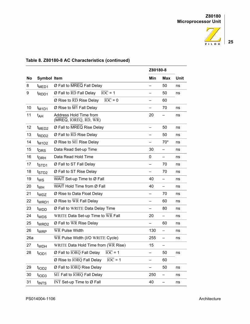
8 tMED1 Ø Fall to MREQ Fall Delay – 50 ns
9 tRDD1 Ø Fall to RD Fall Delay IOC = 1 – 50 ns
Ø Rise to RD Rise Delay IOC = 0 – 60
10 tM1D1 Ø Rise to M1 Fall Delay – 70 ns
11 tAH Address Hold Time from (MREQ, IOREQ, RD, WR)
20 – ns
12 tMED2 Ø Fall to MREQ Rise Delay – 50 ns
13 tRDD2 Ø Fall to RD Rise Delay – 50 ns
14 tM1D2 Ø Rise to M1 Rise Delay – 70* ns
15 tDRS Data Read Set-up Time 30 – ns
16 tDRH Data Read Hold Time 0 – ns
17 tSTD1 Ø Fall to ST Fall Delay – 70 ns
18 tSTD2 Ø Fall to ST Rise Delay – 70 ns
19 tWS WAIT Set-up Time to Ø Fall 40 – ns
20 tWH WAIT Hold Time from Ø Fall 40 – ns
21 tWDZ Ø Rise to Data Float Delay – 70 ns
22 tWRD1 Ø Rise to WR Fall Delay – 60 ns
23 tWDD Ø Fall to WRITE Data Delay Time – 80 ns
24 tWDS WRITE Data Set-up Time to WR Fall 20 – ns
25 tWRD2 Ø Fall to WR Rise Delay – 60 ns
26 tWRP WR Pulse Width 130 – ns
26a WR Pulse Width (I/O WRITE Cycle) 255 – ns
27 tWDH WRITE Data Hold Time from (WR Rise) 15 –
28 tIOD1 Ø Fall to IORQ Fall Delay IOC = 1 – 50 ns
Ø Rise to IORQ Fall Delay IOC = 1 – 60
29 tIOD2 Ø Fall to IORQ Rise Delay – 50 ns
30 tIOD3 M1 Fall to IORQ Fall Delay 250 – ns
31 tINTS INT Set-up Time to Ø Fall 40 – ns
Table 8. Z80180-8 AC Characteristics (continued)
No Symbol Item
Z80180-8
UnitMin Max
PS014004-1106 Architecture
Z80180Microprocessor Unit
26
32 tINTS INT Hold Time from Ø Fall 40 – ns
33 tNMIW NMI Pulse Width 100 – ns
34 tBRS BUSREQ Set-up Time to Ø Fall 40 – ns
35 tBRH BUSREQ Hold Time from Ø Fall 40 ns
36 tBAD1 Ø Rise to BUSACK Fall Delay – 70 ns
37 tBAD2 Ø Fall to BUSACK Rise Delay – 70 ns
38 tBZD Ø Rise to Bus Floating Delay Time – 90 ns
39 tMEWH MREQ Pulse Width (High) 90 – ns
40 tMEWL MREQ Pulse Width (Low) 100 – ns
41 tRFD1 Ø Rise to RFSH Fall Delay – 80 ns
42 tRFD2 Ø Rise to RFSH Rise Delay – 80 ns
43 tHAD1 Ø Rise to HALT Fall Delay – 80 ns
44 tHAD2 Ø Rise to HALT Rise Delay – 80 ns
45 tDRQS /DREQi Set-up Time to Ø Rise 40 – ns
46 tDRQH /DREQi Hold Time from Ø Rise 40 – ns
47 tTED1 Ø Fall to TENDi Fall Delay – 60 ns
48 tTED2 Ø Fall to TENDi Rise Delay – 60 ns
49 tED1 Ø Rise to E Rise Delay – 70 ns
50 tED2 Ø Fall or Rise to E Fall Delay – 70 ns
51 PWEH E Pulse Width (High) 65 – ns
52 PWEL E Pulse Width (Low) 130 – ns
53 tEr Enable Rise Time – 20 ns
54 tEf Enable Fall Time – 20 ns
55 tTOD Ø Fall to Timer Output Delay – 200 ns
56 tSTDI CSIO Transmit Data Delay Time (Internal Clock Operation)
– 200 ns
57 tSTDE CSIO Transmit Data Delay Time (External Clock Operation)
– 7.5tcyc+200
ns
Table 8. Z80180-8 AC Characteristics (continued)
No Symbol Item
Z80180-8
UnitMin Max
PS014004-1106 Architecture
Z80180Microprocessor Unit
27
58 tSRSI CSIO Receive Data Set-up Time (Internal Clock Operation)
1 – tcyc
59 tSRHI CSIO Receive Data Hold Time (Internal Clock Operation)
1 – tcyc
60 tSRSE CSIO Receive Data Set-up Time (External Clock Operation)
1 – tcyc
61 tSRHE CSIO Receive Data Hold Time (External Clock Operation)
1 – tcyc
62 tRES RESET Set-up Time to Ø Fall 100 – ns
63 tREH RESET Hold Time from Ø Fall 70 – ns
64 tOSC Oscillator Stabilization Time – 20 ns
65 tEXr External Clock Rise Time (EXTAL) – 25 ns
66 tEXf External Clock Fall Time (EXTAL) – 25 ns
67 tRr RESET Rise Time – 50 ns
68 tRf RESET Fall Time – 50 ns
69 tIr Input Rise Time (except EXTAL, RESET) – 100 ns
70 tIf Input Fall Time (except EXTAL, RESET) – 100 ns
Table 9. Z80180-10 AC Characteristics
No Symbol Item
Z80180-10
UnitMin Max
1 tcyc Clock Cycle Time 100 2000 ns
2 tCHW Clock H Pulse Width 40 – ns
3 tCLW Clock L Pulse Width 40 – ns
4 tcf Clock Fall Time – 10 ns
5 tcr Clock Rise Time – 10 ns
6 tAD ØRise to Address Valid Delay – 70 ns
7 tAS Address Valid to MREQ Fall or IORQ Fall) 10 – ns
Table 8. Z80180-8 AC Characteristics (continued)
No Symbol Item
Z80180-8
UnitMin Max
PS014004-1106 Architecture

Z80180Microprocessor Unit
28
8 tMED1 Ø Fall to MREQ Fall Delay – 50 ns
9 tRDD1 Ø Fall to RD Fall Delay IOC = 1 – 50 ns
Ø Rise to RD Rise Delay IOC = 0 – 55
10 tM1D1 Ø Rise to M1 Fall Delay – 60 ns
11 tAH Address Hold Time from (MREQ, IOREQ, RD, WR)
10 – ns
12 tMED2 Ø Fall to MREQ Rise Delay – 50 ns
13 tRDD2 Ø Fall to RD Rise Delay – 50 ns
14 tM1D2 Ø Rise to M1 Rise Delay – 60 ns
15 tDRS Data Read Set-up Time 25 – ns
16 tDRH Data Read Hold Time 0 – ns
17 tSTD1 Ø Fall to ST Fall Delay – 60 ns
18 tSTD2 Ø Fall to ST Rise Delay – 60 ns
19 tWS WAIT Set-up Time to Ø Fall 30 – ns
20 tWH WAIT Hold Time from Ø Fall 30 – ns
21 tWDZ Ø Rise to Data Float Delay – 60 ns
22 tWRD1 Ø Rise to WR Fall Delay – 50 ns
23 tWDD Ø Fall to WRITE Data Delay Time – 60 ns
24 tWDS WRITE Data Set-up Time to WR Fall 15 – ns
25 tWRD2 Ø Fall to WR Rise Delay – 50 ns
26 tWRP WR Pulse Width 110 – ns
26a WR Pulse Width (I/O WRITE Cycle) 210 – ns
27 tWDH WRITE Data Hold Time from (WR Rise) 10 –
28 tIOD1 Ø Fall to IORQ Fall Delay IOC = 1 – 50 ns
Ø Rise to IORQ Fall Delay IOC = 1 – 55
29 tIOD2 Ø Fall to IORQ Rise Delay – 50 ns
30 tIOD3 M1 Fall to IORQ Fall Delay 200 – ns
31 tINTS INT Set-up Time to Ø Fall 30 – ns
Table 9. Z80180-10 AC Characteristics (continued)
No Symbol Item
Z80180-10
UnitMin Max
PS014004-1106 Architecture
Z80180Microprocessor Unit
29
32 tINTS INT Hold Time from Ø Fall 30 – ns
33 tNMIW NMI Pulse Width 80 – ns
34 tBRS BUSREQ Set-up Time to Ø Fall 30 – ns
35 tBRH BUSREQ Hold Time from Ø Fall 30 ns
36 tBAD1 Ø Rise to BUSACK Fall Delay – 60 ns
37 tBAD2 Ø Fall to BUSACK Rise Delay – 60 ns
38 tBZD Ø Rise to Bus Floating Delay Time – 80 ns
39 tMEWH MREQ Pulse Width (High) 70 – ns
40 tMEWL MREQ Pulse Width (Low) 80 – ns
41 tRFD1 Ø Rise to RFSH Fall Delay – 60 ns
42 tRFD2 Ø Rise to RFSH Rise Delay – 60 ns
43 tHAD1 Ø Rise to HALT Fall Delay – 50 ns
44 tHAD2 Ø Rise to HALT Rise Delay – 50 ns
45 tDRQS /DREQi Set-up Time to Ø Rise 30 – ns
46 tDRQH /DREQi Hold Time from Ø Rise 30 – ns
47 tTED1 Ø Fall to TENDi Fall Delay – 50 ns
48 tTED2 Ø Fall to TENDi Rise Delay – 50 ns
49 tED1 Ø Rise to E Rise Delay – 60 ns
50 tED2 Ø Fall or Rise to E Fall Delay – 60 ns
51 PWEH E Pulse Width (High) 55 – ns
52 PWEL E Pulse Width (Low) 110 – ns
53 tEr Enable Rise Time – 20 ns
54 tEf Enable Fall Time – 20 ns
55 tTOD Ø Fall to Timer Output Delay – 150 ns
56 tSTDI CSIO Transmit Data Delay Time (Internal Clock Operation)
– 150 ns
57 tSTDE CSIO Transmit Data Delay Time (External Clock Operation)
– 7.5tcyc+150
ns
Table 9. Z80180-10 AC Characteristics (continued)
No Symbol Item
Z80180-10
UnitMin Max
PS014004-1106 Architecture
Z80180Microprocessor Unit
30
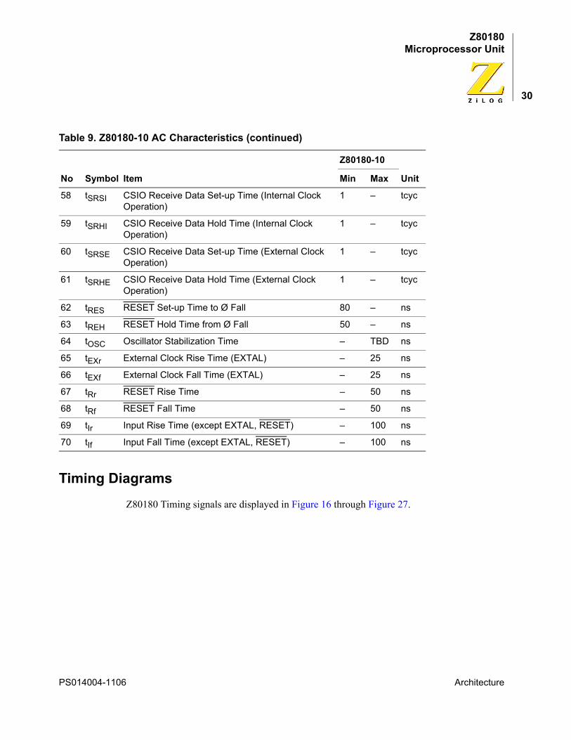
Timing Diagrams
Z80180 Timing signals are displayed in Figure 16 through Figure 27.
58 tSRSI CSIO Receive Data Set-up Time (Internal Clock Operation)
1 – tcyc
59 tSRHI CSIO Receive Data Hold Time (Internal Clock Operation)
1 – tcyc
60 tSRSE CSIO Receive Data Set-up Time (External Clock Operation)
1 – tcyc
61 tSRHE CSIO Receive Data Hold Time (External Clock Operation)
1 – tcyc
62 tRES RESET Set-up Time to Ø Fall 80 – ns
63 tREH RESET Hold Time from Ø Fall 50 – ns
64 tOSC Oscillator Stabilization Time – TBD ns
65 tEXr External Clock Rise Time (EXTAL) – 25 ns
66 tEXf External Clock Fall Time (EXTAL) – 25 ns
67 tRr RESET Rise Time – 50 ns
68 tRf RESET Fall Time – 50 ns
69 tIr Input Rise Time (except EXTAL, RESET) – 100 ns
70 tIf Input Fall Time (except EXTAL, RESET) – 100 ns
Table 9. Z80180-10 AC Characteristics (continued)
No Symbol Item
Z80180-10
UnitMin Max
PS014004-1106 Architecture
Z80180Microprocessor Unit
31
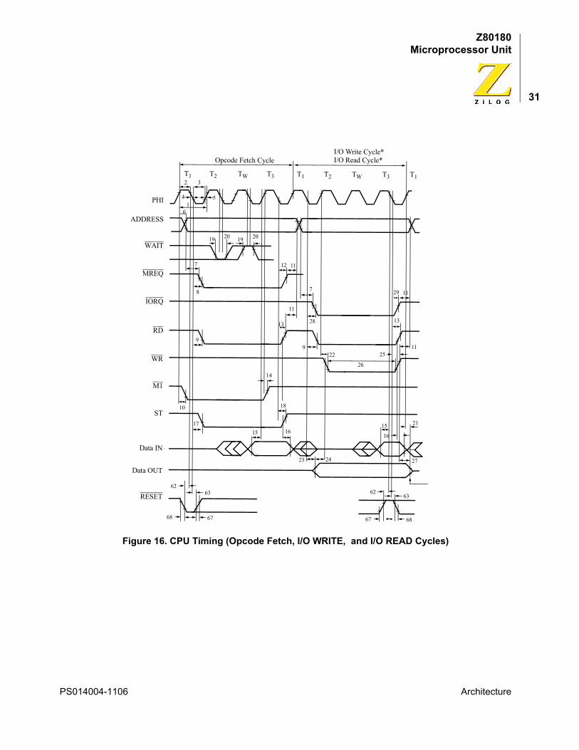
Figure 16. CPU Timing (Opcode Fetch, I/O WRITE, and I/O READ Cycles)
PHI
ADDRESS
WAIT
MREQ
IORQ
RD
WR
M1
ST
Data IN
Data OUT
RESET
11
67 68
6263
68 67
6263
15 1617
10
14
9
22
13
11
28
7 29
7
8
2019 1920
1112
6
9
13
2511
Opcode Fetch Cycle
T1
1
2 3
4 5
15
16
21
27
18
I/O Write Cycle*I/O Read Cycle*
T2 TW T3 T1 T2 TW T3 T1
23 24
26
PS014004-1106 Architecture
Z80180Microprocessor Unit
32
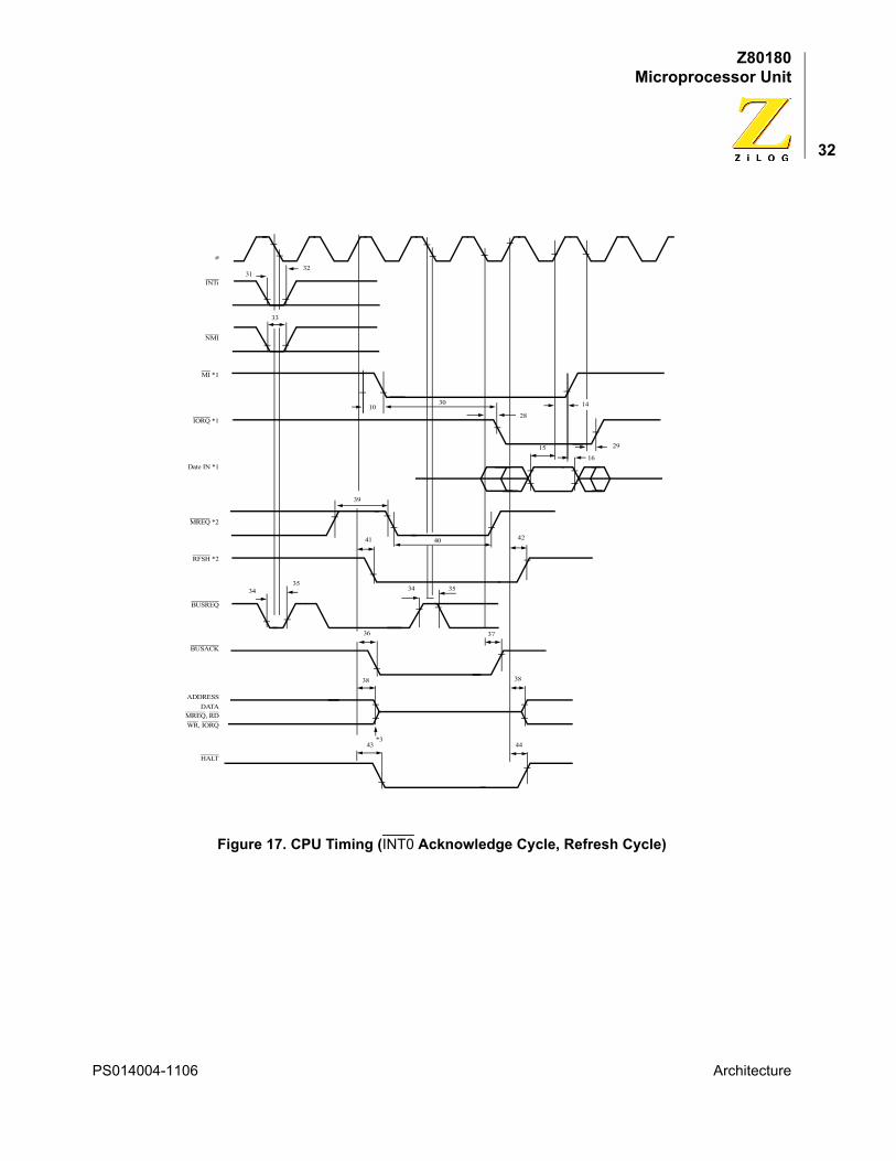
Figure 17. CPU Timing (INT0 Acknowledge Cycle, Refresh Cycle)
ø
INTi31
32
33
40
30
28
1516
29
39
41 42
3435
34 35
36 37
38 38
43 44*3
1410
NMI
MI *1
IORQ *1
Date IN *1
MREQ *2
RFSH *2
BUSREQ
BUSACK
ADDRESSDATA
MREQ, RDWR, IORQ
HALT
PS014004-1106 Architecture
Z80180Microprocessor Unit
33
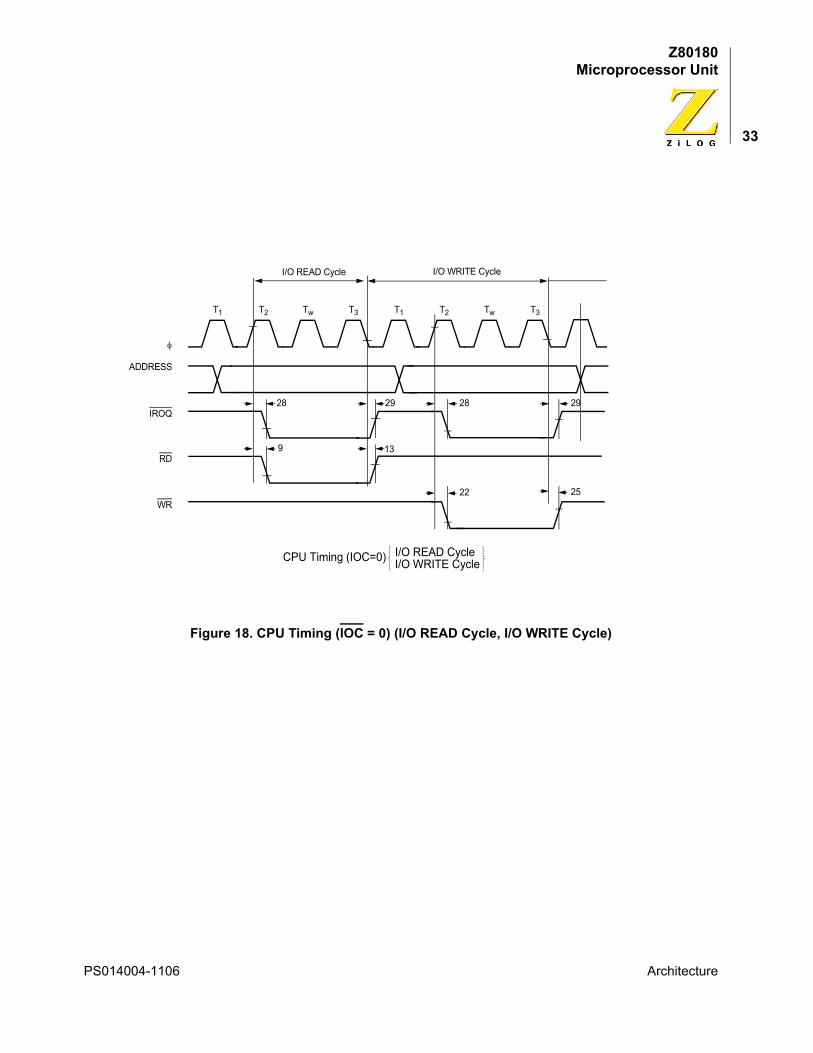
Figure 18. CPU Timing (IOC = 0) (I/O READ Cycle, I/O WRITE Cycle)
CPU Timin= 0) (I/O READ Cycle, I/O WRITE Cycle)
T1 T2 Tw T3 T1 T2 Tw T3
ADDRESS
φ
RD
IROQ
WR
28
9
2928 29
13
22 25
I/O READ Cycle I/O WRITE Cycle
CPU Timing (IOC=0) I/O READ CycleI/O WRITE Cycle
PS014004-1106 Architecture
Z80180Microprocessor Unit
34
Figure 19. DMA Control Signals
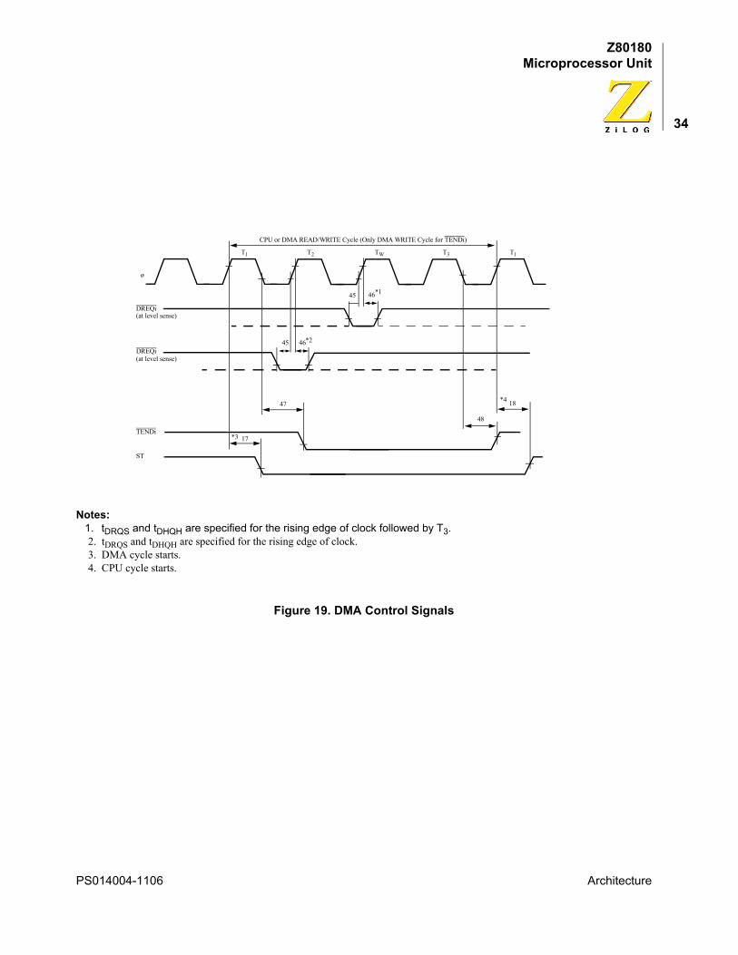
DMA Control Signals
Notes:1. tDRQS and tDHQH are specified for the rising edge of clock followed by T3.2. tDRQS and tDHQH are specified for the rising edge of clock.3. DMA cycle starts.4. CPU cycle starts.
47
45 46
48
18*4
*2
(at level sense)
DREQi(at level sense)
TENDi
ST
ø
T1 T2 TW T3 T1
*3 17
DREQi
CPU or DMA READ/WRITE Cycle (Only DMA WRITE Cycle for TENDi)
45 46*1
PS014004-1106 Architecture
Z80180Microprocessor Unit
35
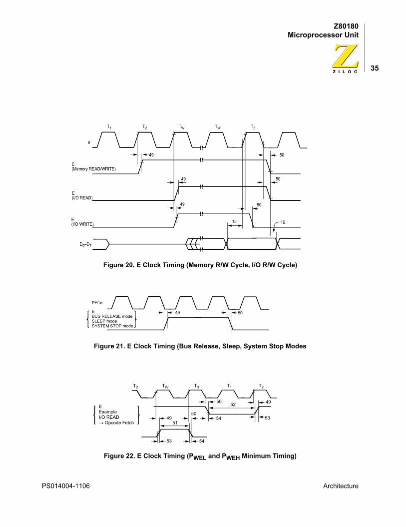
Figure 20. E Clock Timing (Memory R/W Cycle, I/O R/W Cycle)
Figure 21. E Clock Timing (Bus Release, Sleep, System Stop Modes
E Clock Timing (Bus Release, Sleep, System Stop Modes)
Figure 22. E Clock Timing (PWEL and PWEH Minimum Timing)
E Clock Timing (Memory READ/WRITE Cycle, I/O READ/WRITE Cycle)
E
E Clock Timing (Minimum timing example of
49
49
49
15
50
50
50
16
D0–D7
E(Memory READ/WRITE)
E(I/O READ)
E(I/O WRITE)
ø
~~~~
~~~~
~~~~
T1 T2 TW TW T3
PH1ø
EBUS RELEASE modeSLEEP modeSYSTEM STOP mode
49 50
50
52
53
49 53
T2T2 TW T3 T1
54
49
51
54
50EExampleI/O READ→ Opcode Fetch
PS014004-1106 Architecture
Z80180Microprocessor Unit
36
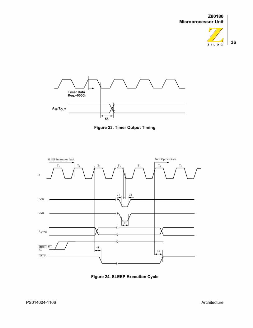
Figure 23. Timer Output Timing
Figure 24. SLEEP Execution Cycle
Timer Output Timing
Execution Cycle
55
Timer DataReg.=0000h
A18/TOUT
32
4443
33
A0–A18
SLEEP Instruction fetch
MREQ, M1
NMI
INTi
HALT
ø
~~~~
~~~~
~~
T1 T2 TS TST3 T1 T2
31
RD
Next Opcode fetch
~~~~
PS014004-1106 Architecture
Z80180Microprocessor Unit
37
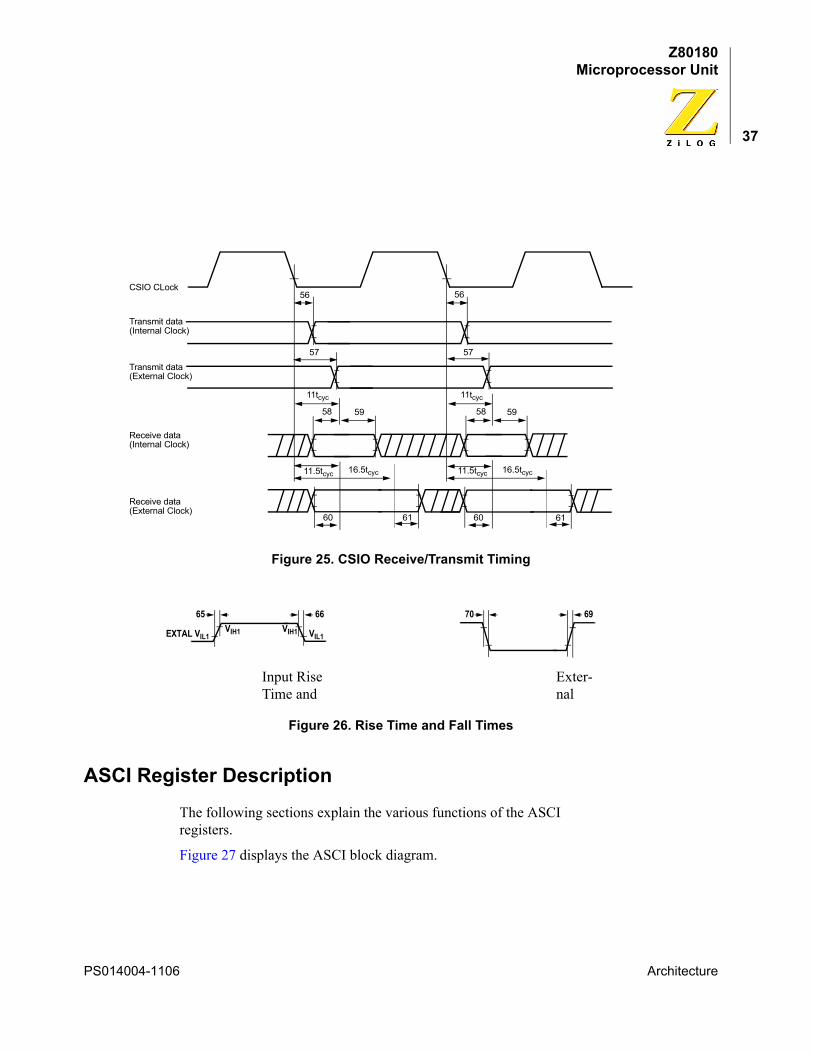
Figure 25. CSIO Receive/Transmit Timing
Figure 26. Rise Time and Fall Times
ASCI Register Description
The following sections explain the various functions of the ASCI registers.
Figure 27 displays the ASCI block diagram.
CSIO Receive/Transmit Timing
Rise Time and Fall Times
57
56
58
56
11.5tcyc
Transmit data
5958 59
11.5tcyc
11tcyc
16.5tcyc
11tcyc
16.5tcyc
57
60 6160 61
(External Clock)
Transmit data(Internal Clock)
Receive data(External Clock)
Receive data(Internal Clock)
CSIO CLock
65 66
VIL1VIH1EXTAL VIL1
VIH1
70 69
Input Rise Time and
Exter-nal
PS014004-1106 Architecture
Z80180Microprocessor Unit
38
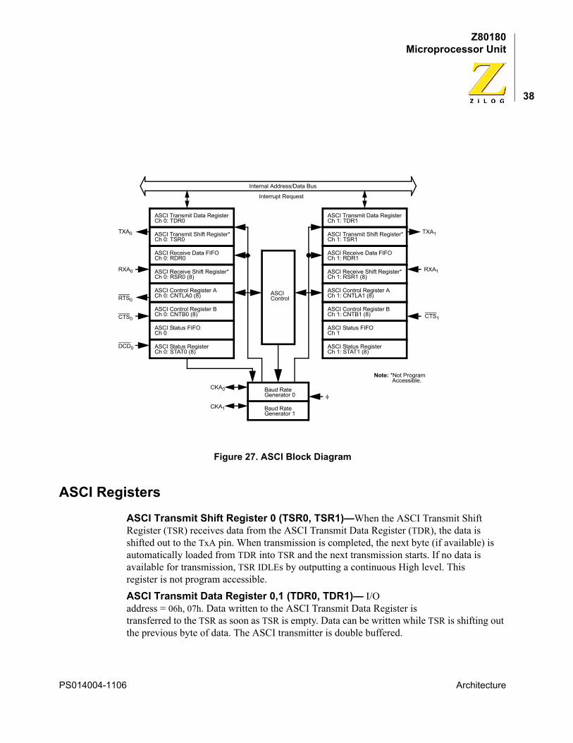
Figure 27. ASCI Block Diagram
ASCI Registers
ASCI Transmit Shift Register 0 (TSR0, TSR1)—When the ASCI Transmit Shift Register (TSR) receives data from the ASCI Transmit Data Register (TDR), the data is shifted out to the TxA pin. When transmission is completed, the next byte (if available) is automatically loaded from TDR into TSR and the next transmission starts. If no data is available for transmission, TSR IDLEs by outputting a continuous High level. This register is not program accessible.ASCI Transmit Data Register 0,1 (TDR0, TDR1)— I/O address = 06h, 07h. Data written to the ASCI Transmit Data Register is transferred to the TSR as soon as TSR is empty. Data can be written while TSR is shifting out the previous byte of data. The ASCI transmitter is double buffered.
ASCI Block Diagram
Internal Address/Data Bus
ASCI Transmit Data RegisterCh 0: TDR0
ASCI Transmit Shift Register*Ch 0: TSR0
ASCI Receive Data FIFOCh 0: RDR0
ASCI Receive Shift Register*Ch 0: RSR0 (8)
ASCI Control Register ACh 0: CNTLA0 (8)
ASCI Control Register BCh 0: CNTB0 (8)
ASCI Status RegisterCh 0: STAT0 (8)
ASCI Status FIFOCh 0
ASCI Transmit Data RegisterCh 1: TDR1
ASCI Transmit Shift Register*Ch 1: TSR1
ASCI Receive Data FIFOCh 1: RDR1
ASCI Receive Shift Register*Ch 1: RSR1 (8)
ASCI Control Register ACh 1: CNTLA1 (8)
ASCI Control Register BCh 1: CNTB1 (8)
ASCI Status RegisterCh 1: STAT1 (8)
ASCI Status FIFOCh 1
TXA0
RXA0
RTS0
CTS0
DCD0
TXA1
RXA1
CTS1
ASCIControl
Baud RateGenerator 0
Baud RateGenerator 1
CKA0
CKA1
φ
Note: *Not Program
Interrupt Request
Accessible.
PS014004-1106 Architecture
Z80180Microprocessor Unit
39
Data can be written into and read from the ASCI Transmit Data Register. If data is read from the ASCI Transmit Data Register, the ASCI data transmit operation is not affected by this READ operation.ASCI Receive Shift Register 0,1 (RSR0, RSR1)—This register receives data shifted in on the RxA pin. When full, data is automatically transferred to the ASCI Receive Data Register (RDR) if it is empty. If RSR is not empty when the next incoming data byte is shifted in, an overrun error occurs. This register is not program accessible.ASCI Receive Data FIFO 0,1 (RDR0, RDR1)—I/O Address = 08h, 09h. The ASCI Receive Data Register is a READ-ONLY register. When a complete incoming data byte is assembled in RSR, it is automatically transferred to the 4 character Receive Data First-In First-Out (FIFO) memory. The oldest character in the FIFO (if any) can be read from the Receive Data Register (RDR). The next incoming data byte can be shifted into RSR while the FIFO is full. The ASCI receiver is well buffered.
ASCI Transmit Data Registers
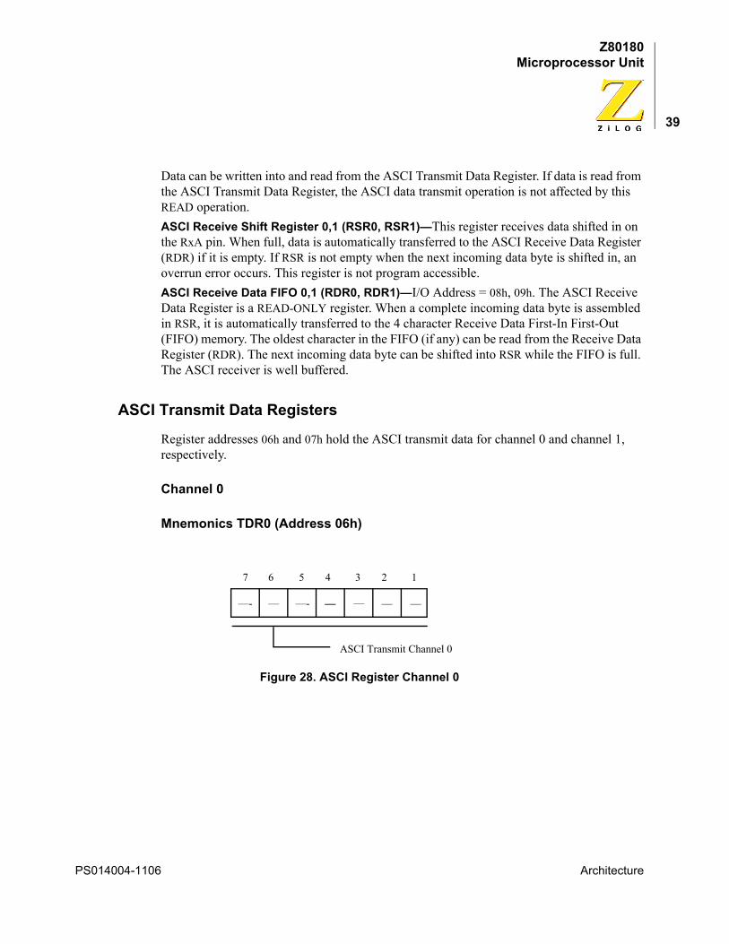
Register addresses 06h and 07h hold the ASCI transmit data for channel 0 and channel 1, respectively.
Channel 0
Mnemonics TDR0 (Address 06h)
Figure 28. ASCI Register Channel 0
ASCI Transmit Channel 0
— — — ———- —
7 6 5 4 3 2 1
—-
PS014004-1106 Architecture
Z80180Microprocessor Unit
40
Channel 1
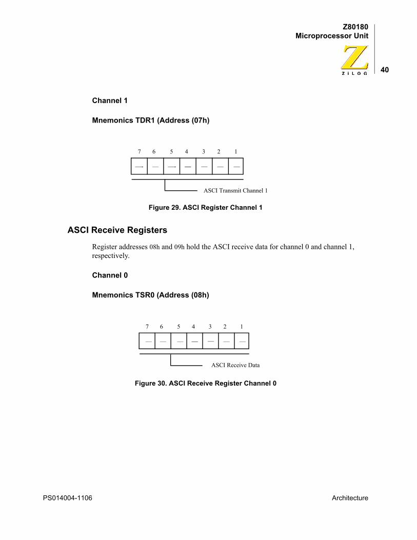
Mnemonics TDR1 (Address (07h)
Figure 29. ASCI Register Channel 1
ASCI Receive Registers
Register addresses 08h and 09h hold the ASCI receive data for channel 0 and channel 1, respectively.
Channel 0
Mnemonics TSR0 (Address (08h)
Figure 30. ASCI Receive Register Channel 0
ASCI Receive Register Channel 0
ASCI Transmit Channel 1
— — — ———- —
7 6 5 4 3 2 1
—-
ASCI Receive Data
— — — ——— — —
7 6 5 4 3 2 1
PS014004-1106 Architecture
Z80180Microprocessor Unit
41
Channel 1
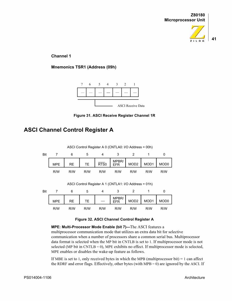
Mnemonics TSR1 (Address (09h)
Figure 31. ASCI Receive Register Channel 1R
ASCI Channel Control Register A
Figure 32. ASCI Channel Control Register A
MPE: Multi-Processor Mode Enable (bit 7)—The ASCI features a multiprocessor communication mode that utilizes an extra data bit for selective communication when a number of processors share a common serial bus. Multiprocessor data format is selected when the MP bit in CNTLB is set to 1. If multiprocessor mode is not selected (MP bit in CNTLB = 0), MPE exhibits no effect. If multiprocessor mode is selected, MPE enables or disables the wake-up feature as follows.
If MBE is set to 1, only received bytes in which the MPB (multiprocessor bit) = 1 can affect the RDRF and error flags. Effectively, other bytes (with MPB = 0) are ignored by the ASCI. If
ASCI Receive Register Channel 1R
ASCI Channel Control Register A
ASCI Receive Data
— — — ——— — —
7 6 5 4 3 2 1
Bit
MPE RE
R/W R/W R/W
TE
7 6 5 4 3 2 1 0
RTS0MPBR/
MOD2 MOD1 MOD0
R/W R/W
ASCI Control Register A 0 (CNTLA0: I/O Address = 00h)
R/W R/W R/W
EFR
Bit
MPE RE
R/W R/W R/W
TE
7 6 5 4 3 2 1 0
__ MOD2 MOD1 MOD0
R/W R/W
ASCI Control Register A 1 (CNTLA1: I/O Address = 01h)
R/W R/W R/W
MPBR/EFR
PS014004-1106 Architecture
Z80180Microprocessor Unit
42
MPE is reset to 0, all bytes, regardless of the state of the MPB data bit, affect the REDR and error flags. MPE is cleared to 0 during RESET.RE: Receiver Enable (bit 6)—When RE is set to 1, the ASCI transmitter is enabled. When TE is reset to 0, the transmitter is disables and any transmit operation in progress is interrupted. However, the TDRE flag is not reset and the previous contents of TDRE are held. TE is cleared to 0 in IOSTOP mode during RESET.TE: Transmitter Enable (bit 5)—When TE is set to 1, the ASCI receiver is enabled. When TE is reset to 0, the transmitter is disabled and any transmit operation in progress is interrupted. However, the TDRE flag is not reset and the previous contents of TDRE are held. TE is cleared to 0 in IOSTOP mode during RESET.RTS0: Request to Send Channel 0 (bit 4 in CNTLA0 only)—If bit 4 of the System Configuration Register is 0, the RTS0/TxS pin features the RTS0 function. RTS0 allows the ASCI to control (START/STOP) another communication devices transmission (for example, by connecting to that device’s CTS input). RTS0 is essentially a 1 bit output port, having no side effects on other ASCI registers or flags. Bit 4 in CNTLA1 is not used.MPBR/EFR: Multiprocessor Bit Receive/Error Flag Reset (bit 3)—When multiprocessor mode is enabled (MP in CNTLB = 1), MPBR, when read, contains the value of the MPB bit for the most recent receive operation. When written to 0, the EFR function is selected to reset all error flags (OVRN, FE, PE and BRK in the ASEXT register) to 0. MPBR/EFR is undefined during RESET.MOD2, 1, 0: ASCI Data Format Mode 2, 1, 0 (bits 2–0)—These bits program the ASCI data format as listed in Table 10.
The data formats available based on all combinations of MOD2, MOD1, and MOD0 are indicated in Table 11.
Table 10. ASCI Data Formats Mode 2, 1, 0
Bit Description
MOD2 = 0 0→7 bit data
MOD2 = 1 1→8 bit data
MOD1 = 0 0→No parity
MOD1 = 1 1→Parity enabled
MOD0 = 0 0→1 stop bit
MOD0 = 1 1→2 stop bits
PS014004-1106 Architecture
Z80180Microprocessor Unit
43
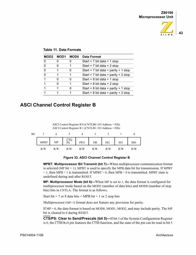
ASCI Channel Control Register B
Figure 33. ASCI Channel Control Register B
MPBT: Multiprocessor Bit Transmit (bit 7)—When multiprocessor communication format is selected (MP bit = 1), MPBT is used to specify the MPB data bit for transmission. If MPBT = 1, then MPB = 1 is transmitted. If MPBT = 0, then MPB = 0 is transmitted. MPBT state is undefined during and after RESET.MP: Multiprocessor Mode (bit 6)—When MP is set to 1, the data format is configured for multiprocessor mode based on the MOD2 (number of data bits) and MOD0 (number of stop bits) bits in CNTLA. The format is as follows.
Start bit + 7 or 8 data bits + MPB bit + 1 or 2 stop bits
Multiprocessor (MP=1) format does not feature any provision for parity.
If MP = 0, the data format is based on MOD0, MOD1, MOD2, and may include parity. The MP bit is cleared to 0 during RESET.CTS/PS: Clear to Send/Prescale (bit 5)—If bit 5 of the System Configuration Register is 0, the CTS0/RxS pin features the CTS0 function, and the state of the pin can be read in bit 5
Table 11. Data Formats
MOD2 MOD1 MOD0 Data Format0 0 0 Start + 7 bit data + 1 stop0 0 1 Start + 7 bit data + 2 stop0 1 0 Start + 7 bit data + parity + 1 stop0 1 1 Start + 7 bit data + parity + 2 stop1 0 0 Start + 8 bit data + 1 stop1 0 1 Start + 8 bit data + 2 stop1 1 0 Start + 8 bit data + parity + 1 stop1 1 1 Start + 8 bit data + parity + 2 stop
ASCI Channel Control Register B
Bit
MPBT MP
R/W R/W R/W
CTS/
7 6 5 4 3 2 1 0
PEO DR SS2 SS1 SS0
R/W R/W
ASCI Control Register B 1 (CNTLB1: I/O Address = 03h)
R/W R/W R/W
ASCI Control Register B 0 (CNTLB0: I/O Address = 02h)
PS
PS014004-1106 Architecture
Z80180Microprocessor Unit
44
of CNTLB0 in a real-time, positive-logic fashion (HIGH = 1, LOW = 0). If bit 5 in the System Configuration Register is 0 to auto-enable CTS0, and the pin is negated (High), the TDRE bit is inhibited (forced to 0). Bit 5 of CNTLB1 reads back as 0.
If the SS2–0 bits in this register are not 111, and the BRG mode bit in the ASEXT register is 0, then writing to this bit sets the prescale (PS) control. Under these circumstances, a 0 indi-cates a divide-by-10 prescale function, while a 1 indicates divide-by-30. The bit resets to 0.PEO: Parity Even Odd (bit 4)—PEO selects oven or odd parity. PEO does not affect the enabling/disabling of parity (MOD1 bit of CNTLA). If PEO is cleared to 0, even parity is selected. If PEO is set to 1, odd parity is selected. PEO is cleared to 0 during RESET.DR: Divide Ratio (bit 3)—If the X1 bit in the ASEXT register is 0, this bit specifies the divider used to obtain baud rate from the data sampling clock. If DR is reset to 0, divide- by-16 is used, while if DR is set to 1, divide-by-64 is used. DR is cleared to 0 during RESET.SS2,1,0: Source/Speed Select 2,1,0 (bits 2–0)—If these bits are 111, as they are after RESET, the CKA pin is used as a clock input, and is divided by 1, 16, or 64 depending on the DR bit and the X1 bit in the ASEXT register.
If these bits are not 111 and the BRG mode bit is ASEXT is 0, these bits specify a power-of-two divider for the PHI clock as indicated in Table 12.
Setting or leaving these bits as 111 makes sense for a channel only when its CKA pin is selected for the CKA function. CKAO/CKS features the CKAO function when bit 4 of the System Configuration Register is 0. DCD0/CKA1 features the CKA1 function when bit 0 of the Interrupt Edge register is 1.
Table 12. Divide Ratio
SS2 SS1 SS0 Divide Ratio
0 0 0 ÷1
0 0 1 ÷2
0 1 0 ÷4
0 1 1 ÷8
1 0 0 ÷16
1 0 1 ÷32
1 1 0 ÷64
1 1 1 External Clock
PS014004-1106 Architecture
Z80180Microprocessor Unit
45
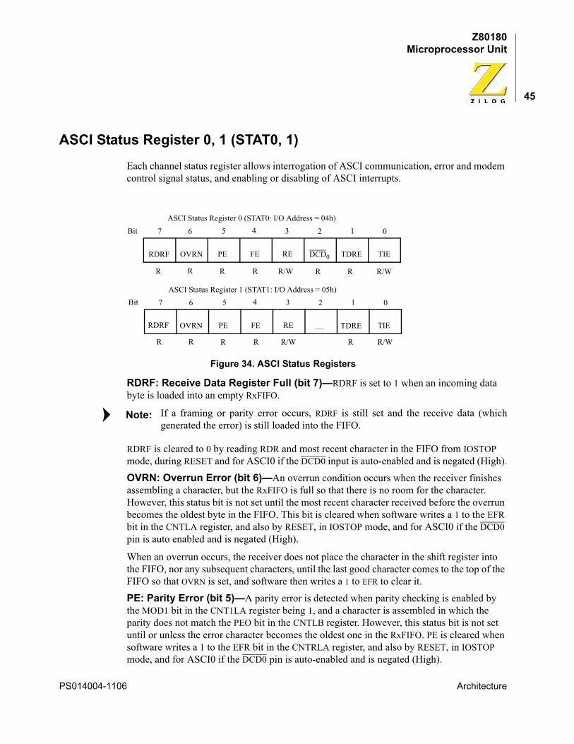
ASCI Status Register 0, 1 (STAT0, 1)
Each channel status register allows interrogation of ASCI communication, error and modem control signal status, and enabling or disabling of ASCI interrupts.
Figure 34. ASCI Status Registers
RDRF: Receive Data Register Full (bit 7)—RDRF is set to 1 when an incoming data byte is loaded into an empty RxFIFO.
If a framing or parity error occurs, RDRF is still set and the receive data (whichgenerated the error) is still loaded into the FIFO.
RDRF is cleared to 0 by reading RDR and most recent character in the FIFO from IOSTOP mode, during RESET and for ASCI0 if the DCD0 input is auto-enabled and is negated (High).OVRN: Overrun Error (bit 6)—An overrun condition occurs when the receiver finishes assembling a character, but the RxFIFO is full so that there is no room for the character. However, this status bit is not set until the most recent character received before the overrun becomes the oldest byte in the FIFO. This bit is cleared when software writes a 1 to the EFR bit in the CNTLA register, and also by RESET, in IOSTOP mode, and for ASCI0 if the DCD0 pin is auto enabled and is negated (High).
When an overrun occurs, the receiver does not place the character in the shift register into the FIFO, nor any subsequent characters, until the last good character comes to the top of the FIFO so that OVRN is set, and software then writes a 1 to EFR to clear it.PE: Parity Error (bit 5)—A parity error is detected when parity checking is enabled by the MOD1 bit in the CNT1LA register being 1, and a character is assembled in which the parity does not match the PEO bit in the CNTLB register. However, this status bit is not set until or unless the error character becomes the oldest one in the RxFIFO. PE is cleared when software writes a 1 to the EFR bit in the CNTRLA register, and also by RESET, in IOSTOP mode, and for ASCI0 if the DCD0 pin is auto-enabled and is negated (High).
ASCI Status Registers
Bit
RDRF OVRN
R R R/W
PE
7 6 5 4 3 2 1 0
FE RE DCD0 TDRE TIE
R R
ASCI Status Register 0 (STAT0: I/O Address = 04h)
R R R/W
Bit
RDRF OVRN
R R/W
PE
7 6 5 4 3 2 1 0
FE RE TDRE TIE
R R
ASCI Status Register 1 (STAT1: I/O Address = 05h)
R R R/W
__
Note:
PS014004-1106 Architecture
Z80180Microprocessor Unit
46
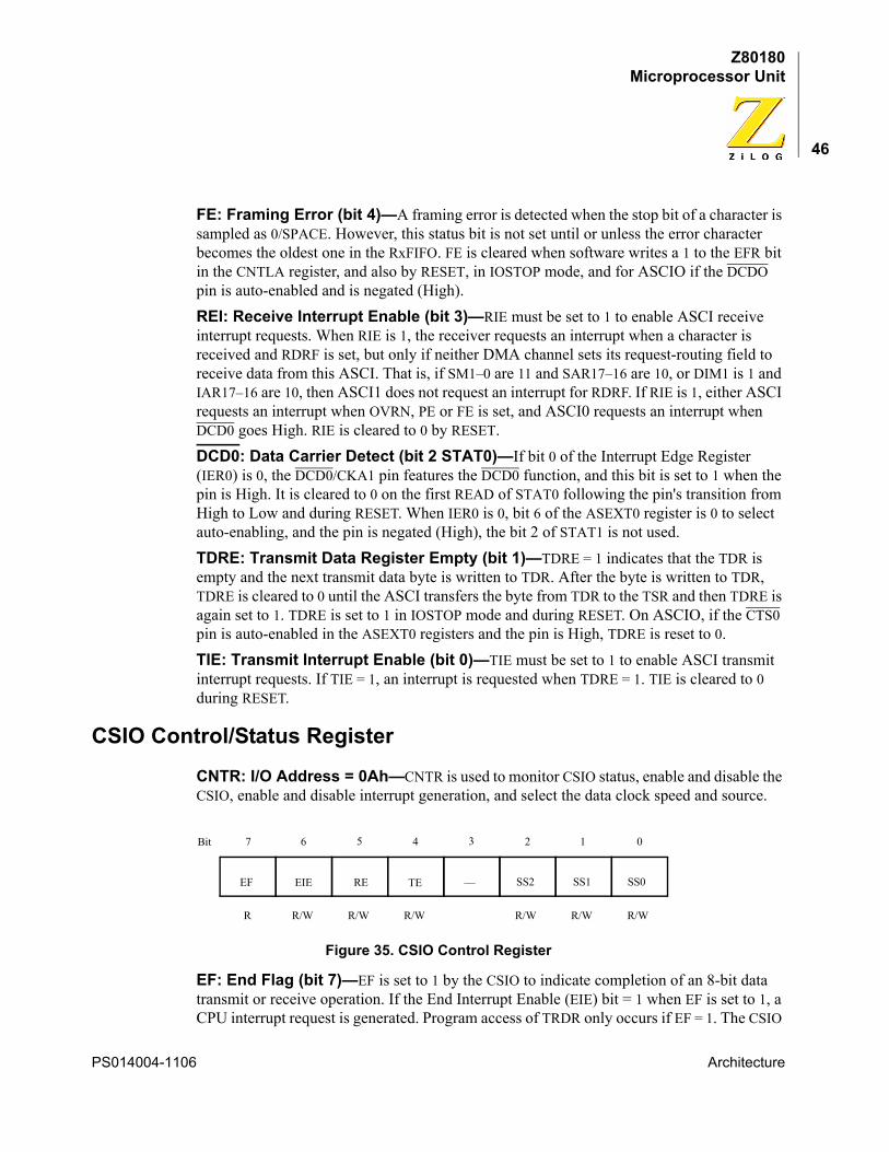
FE: Framing Error (bit 4)—A framing error is detected when the stop bit of a character is sampled as 0/SPACE. However, this status bit is not set until or unless the error character becomes the oldest one in the RxFIFO. FE is cleared when software writes a 1 to the EFR bit in the CNTLA register, and also by RESET, in IOSTOP mode, and for ASCIO if the DCDO pin is auto-enabled and is negated (High).REI: Receive Interrupt Enable (bit 3)—RIE must be set to 1 to enable ASCI receive interrupt requests. When RIE is 1, the receiver requests an interrupt when a character is received and RDRF is set, but only if neither DMA channel sets its request-routing field to receive data from this ASCI. That is, if SM1–0 are 11 and SAR17–16 are 10, or DIM1 is 1 and IAR17–16 are 10, then ASCI1 does not request an interrupt for RDRF. If RIE is 1, either ASCI requests an interrupt when OVRN, PE or FE is set, and ASCI0 requests an interrupt when DCD0 goes High. RIE is cleared to 0 by RESET.DCD0: Data Carrier Detect (bit 2 STAT0)—If bit 0 of the Interrupt Edge Register (IER0) is 0, the DCD0/CKA1 pin features the DCD0 function, and this bit is set to 1 when the pin is High. It is cleared to 0 on the first READ of STAT0 following the pin's transition from High to Low and during RESET. When IER0 is 0, bit 6 of the ASEXT0 register is 0 to select auto-enabling, and the pin is negated (High), the bit 2 of STAT1 is not used.TDRE: Transmit Data Register Empty (bit 1)—TDRE = 1 indicates that the TDR is empty and the next transmit data byte is written to TDR. After the byte is written to TDR, TDRE is cleared to 0 until the ASCI transfers the byte from TDR to the TSR and then TDRE is again set to 1. TDRE is set to 1 in IOSTOP mode and during RESET. On ASCIO, if the CTS0 pin is auto-enabled in the ASEXT0 registers and the pin is High, TDRE is reset to 0.TIE: Transmit Interrupt Enable (bit 0)—TIE must be set to 1 to enable ASCI transmit interrupt requests. If TIE = 1, an interrupt is requested when TDRE = 1. TIE is cleared to 0 during RESET.
CSIO Control/Status Register
CNTR: I/O Address = 0Ah—CNTR is used to monitor CSIO status, enable and disable the CSIO, enable and disable interrupt generation, and select the data clock speed and source.
Figure 35. CSIO Control Register
EF: End Flag (bit 7)—EF is set to 1 by the CSIO to indicate completion of an 8-bit data transmit or receive operation. If the End Interrupt Enable (EIE) bit = 1 when EF is set to 1, a CPU interrupt request is generated. Program access of TRDR only occurs if EF = 1. The CSIO
CSIO Control
Bit
EF EIE
R/W R/W R/W
RE
7 6 5 4 3 2 1 0
TE __ SS2 SS1 SS0
R R/W R/W R/W
PS014004-1106 Architecture
Z80180Microprocessor Unit
47
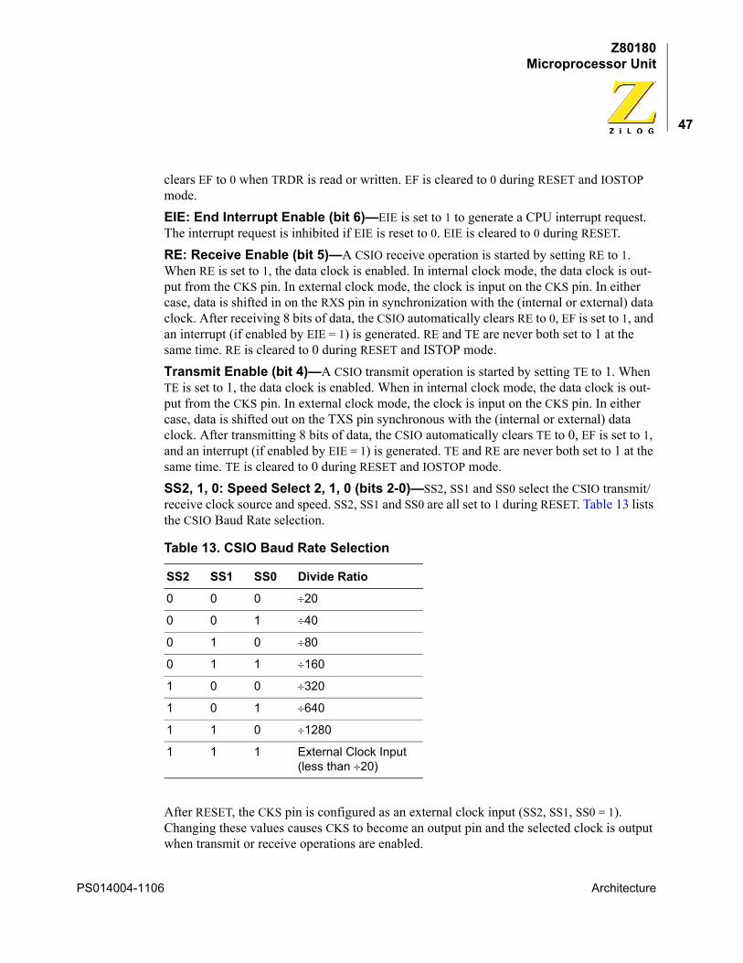
clears EF to 0 when TRDR is read or written. EF is cleared to 0 during RESET and IOSTOP mode.EIE: End Interrupt Enable (bit 6)—EIE is set to 1 to generate a CPU interrupt request. The interrupt request is inhibited if EIE is reset to 0. EIE is cleared to 0 during RESET.RE: Receive Enable (bit 5)—A CSIO receive operation is started by setting RE to 1. When RE is set to 1, the data clock is enabled. In internal clock mode, the data clock is out-put from the CKS pin. In external clock mode, the clock is input on the CKS pin. In either case, data is shifted in on the RXS pin in synchronization with the (internal or external) data clock. After receiving 8 bits of data, the CSIO automatically clears RE to 0, EF is set to 1, and an interrupt (if enabled by EIE = 1) is generated. RE and TE are never both set to 1 at the same time. RE is cleared to 0 during RESET and ISTOP mode.Transmit Enable (bit 4)—A CSIO transmit operation is started by setting TE to 1. When TE is set to 1, the data clock is enabled. When in internal clock mode, the data clock is out-put from the CKS pin. In external clock mode, the clock is input on the CKS pin. In either case, data is shifted out on the TXS pin synchronous with the (internal or external) data clock. After transmitting 8 bits of data, the CSIO automatically clears TE to 0, EF is set to 1, and an interrupt (if enabled by EIE = 1) is generated. TE and RE are never both set to 1 at the same time. TE is cleared to 0 during RESET and IOSTOP mode.SS2, 1, 0: Speed Select 2, 1, 0 (bits 2-0)—SS2, SS1 and SS0 select the CSIO transmit/receive clock source and speed. SS2, SS1 and SS0 are all set to 1 during RESET. Table 13 lists the CSIO Baud Rate selection.
After RESET, the CKS pin is configured as an external clock input (SS2, SS1, SS0 = 1). Changing these values causes CKS to become an output pin and the selected clock is output when transmit or receive operations are enabled.
Table 13. CSIO Baud Rate Selection
SS2 SS1 SS0 Divide Ratio
0 0 0 ÷20
0 0 1 ÷40
0 1 0 ÷80
0 1 1 ÷160
1 0 0 ÷320
1 0 1 ÷640
1 1 0 ÷1280
1 1 1 External Clock Input (less than ÷20)
PS014004-1106 Architecture
Z80180Microprocessor Unit
48
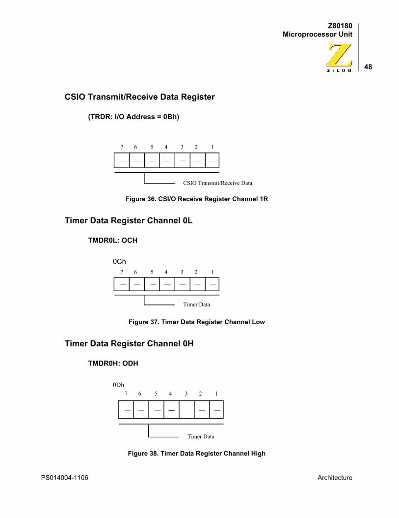
CSIO Transmit/Receive Data Register
(TRDR: I/O Address = 0Bh)
Figure 36. CSI/O Receive Register Channel 1R
Timer Data Register Channel 0L
TMDR0L: OCH
Figure 37. Timer Data Register Channel Low
Timer Data Register Channel 0H
TMDR0H: ODH
Figure 38. Timer Data Register Channel High
ASCI Receive Register Channel 1R
ASCI Receive Register Channel 1R
0Ch
Timer Data Register Channel High
0Dh
CSIO Transmit/Receive Data
— — — ——— — —
7 6 5 4 3 2 1
Timer Data
— — — ——— — —
7 6 5 4 3 2 1
Timer Data
— — — ——— — —
7 6 5 4 3 2 1
PS014004-1106 Architecture
Z80180Microprocessor Unit
49
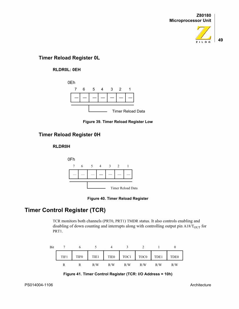
Timer Reload Register 0L
RLDR0L: 0EH
Figure 39. Timer Reload Register Low
Timer Reload Register 0H
RLDR0H
Figure 40. Timer Reload Register
Timer Control Register (TCR)
TCR monitors both channels (PRT0, PRT1) TMDR status. It also controls enabling and disabling of down counting and interrupts along with controlling output pin A18/TOUT for PRT1.
Figure 41. Timer Control Register (TCR: I/O Address = 10h)
Timer Reload Register Low
0Eh
Timer Reload Register
0Fh
Timer Control Register (TCR: I/O Address = 10h)
Timer Reload Data
— — — ——— — —
7 6 5 4 3 2 1
Timer Reload Data
— — — ——— — —
7 6 5 4 3 2 1
Bit
TIF1 TIF0
R/W R/W R/W
TIE1
7 6 5 4 3 2 1 0
TIE0 TOC0 TDE1 TDE0
R R R/W R/W R/W
TOC1
PS014004-1106 Architecture
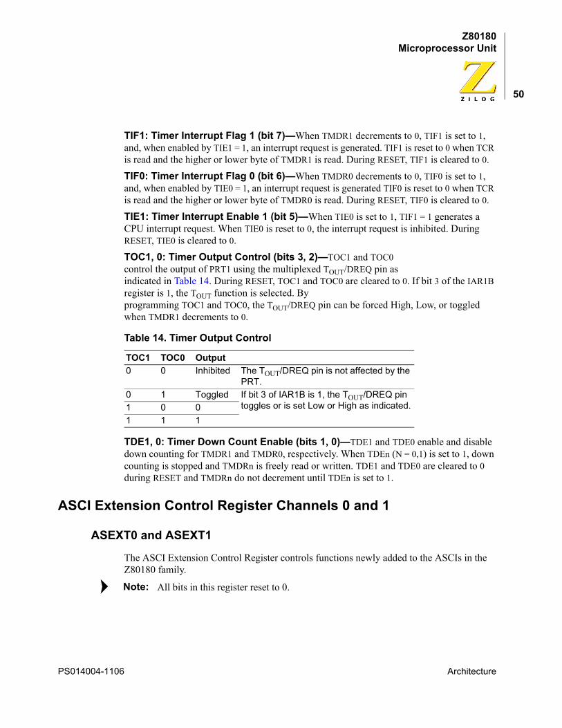
Z80180Microprocessor Unit
50
TIF1: Timer Interrupt Flag 1 (bit 7)—When TMDR1 decrements to 0, TIF1 is set to 1, and, when enabled by TIE1 = 1, an interrupt request is generated. TIF1 is reset to 0 when TCR is read and the higher or lower byte of TMDR1 is read. During RESET, TIF1 is cleared to 0.TIF0: Timer Interrupt Flag 0 (bit 6)—When TMDR0 decrements to 0, TIF0 is set to 1, and, when enabled by TIE0 = 1, an interrupt request is generated TIF0 is reset to 0 when TCR is read and the higher or lower byte of TMDR0 is read. During RESET, TIF0 is cleared to 0.TIE1: Timer Interrupt Enable 1 (bit 5)—When TIE0 is set to 1, TIF1 = 1 generates a CPU interrupt request. When TIE0 is reset to 0, the interrupt request is inhibited. During RESET, TIE0 is cleared to 0.TOC1, 0: Timer Output Control (bits 3, 2)—TOC1 and TOC0 control the output of PRT1 using the multiplexed TOUT/DREQ pin as indicated in Table 14. During RESET, TOC1 and TOC0 are cleared to 0. If bit 3 of the IAR1B register is 1, the TOUT function is selected. By programming TOC1 and TOC0, the TOUT/DREQ pin can be forced High, Low, or toggled when TMDR1 decrements to 0.
TDE1, 0: Timer Down Count Enable (bits 1, 0)—TDE1 and TDE0 enable and disable down counting for TMDR1 and TMDR0, respectively. When TDEn (N = 0,1) is set to 1, down counting is stopped and TMDRn is freely read or written. TDE1 and TDE0 are cleared to 0 during RESET and TMDRn do not decrement until TDEn is set to 1.
ASCI Extension Control Register Channels 0 and 1
ASEXT0 and ASEXT1
The ASCI Extension Control Register controls functions newly added to the ASCIs in the Z80180 family.
All bits in this register reset to 0.
Table 14. Timer Output Control
TOC1 TOC0 Output0 0 Inhibited The TOUT/DREQ pin is not affected by the
PRT.0 1 Toggled If bit 3 of IAR1B is 1, the TOUT/DREQ pin
toggles or is set Low or High as indicated.1 0 01 1 1
Note:
PS014004-1106 Architecture
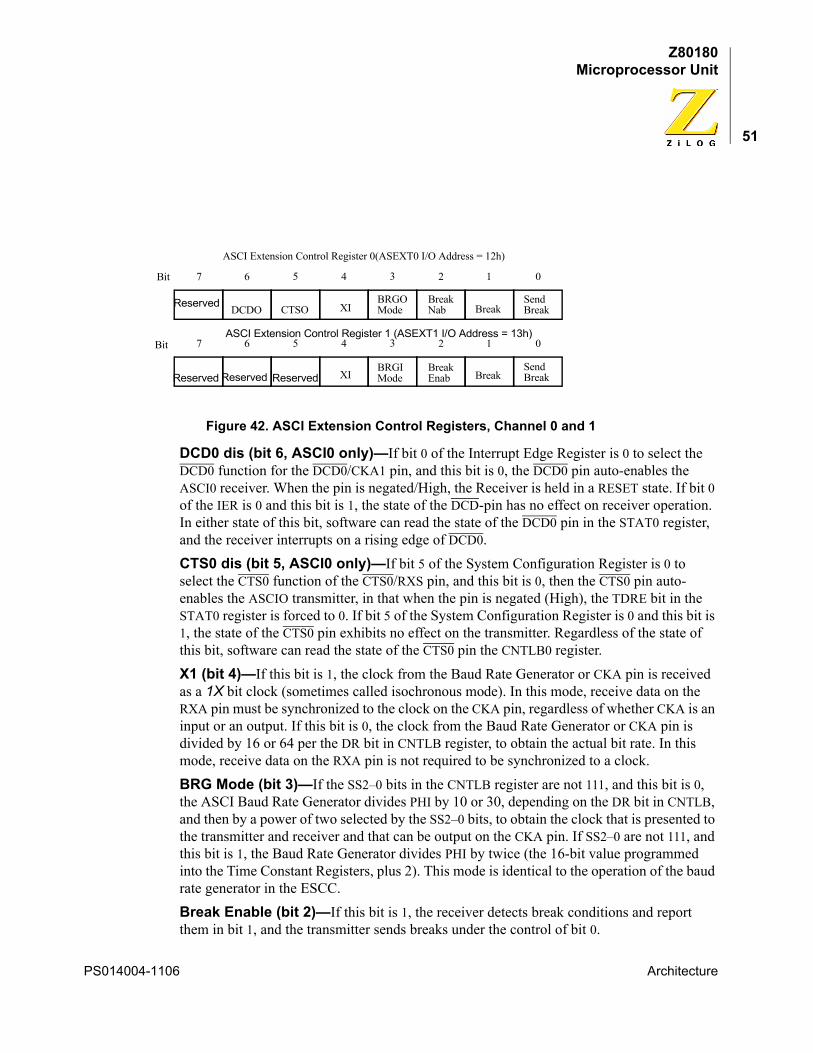
Z80180Microprocessor Unit
51
Figure 42. ASCI Extension Control Registers, Channel 0 and 1
DCD0 dis (bit 6, ASCI0 only)—If bit 0 of the Interrupt Edge Register is 0 to select the DCD0 function for the DCD0/CKA1 pin, and this bit is 0, the DCD0 pin auto-enables the ASCI0 receiver. When the pin is negated/High, the Receiver is held in a RESET state. If bit 0 of the IER is 0 and this bit is 1, the state of the DCD-pin has no effect on receiver operation. In either state of this bit, software can read the state of the DCD0 pin in the STAT0 register, and the receiver interrupts on a rising edge of DCD0.CTS0 dis (bit 5, ASCI0 only)—If bit 5 of the System Configuration Register is 0 to select the CTS0 function of the CTS0/RXS pin, and this bit is 0, then the CTS0 pin auto-enables the ASCIO transmitter, in that when the pin is negated (High), the TDRE bit in the STAT0 register is forced to 0. If bit 5 of the System Configuration Register is 0 and this bit is 1, the state of the CTS0 pin exhibits no effect on the transmitter. Regardless of the state of this bit, software can read the state of the CTS0 pin the CNTLB0 register.X1 (bit 4)—If this bit is 1, the clock from the Baud Rate Generator or CKA pin is received as a 1X bit clock (sometimes called isochronous mode). In this mode, receive data on the RXA pin must be synchronized to the clock on the CKA pin, regardless of whether CKA is an input or an output. If this bit is 0, the clock from the Baud Rate Generator or CKA pin is divided by 16 or 64 per the DR bit in CNTLB register, to obtain the actual bit rate. In this mode, receive data on the RXA pin is not required to be synchronized to a clock.BRG Mode (bit 3)—If the SS2–0 bits in the CNTLB register are not 111, and this bit is 0, the ASCI Baud Rate Generator divides PHI by 10 or 30, depending on the DR bit in CNTLB, and then by a power of two selected by the SS2–0 bits, to obtain the clock that is presented to the transmitter and receiver and that can be output on the CKA pin. If SS2–0 are not 111, and this bit is 1, the Baud Rate Generator divides PHI by twice (the 16-bit value programmed into the Time Constant Registers, plus 2). This mode is identical to the operation of the baud rate generator in the ESCC.Break Enable (bit 2)—If this bit is 1, the receiver detects break conditions and report them in bit 1, and the transmitter sends breaks under the control of bit 0.
ASCI Extension Control Registers, Channel 0 and 1
Bit
DCDO
7 6 5 4 3 2 1 0
XIBRGO Break
BreakSend
ASCI Extension Control Register 0(ASEXT0 I/O Address = 12h)
CTSO Mode Nab Break
Bit 7 6 5 4 3 2 1 0
XIBRGI Break
BreakSend
Mode Enab Break
ASCI Extension Control Register 1 (ASEXT1 I/O Address = 13h)
Reserved
Reserved Reserved Reserved
PS014004-1106 Architecture
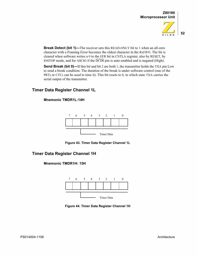
Z80180Microprocessor Unit
52
Break Detect (bit 1)—The receiver sets this READ-ONLY bit to 1 when an all-zero character with a Framing Error becomes the oldest character in the RxFIFO. The bit is cleared when software writes a 0 to the EFR bit in CNTLA register, also by RESET, by IOSTOP mode, and for ASCIO if the DCD0 pin is auto-enabled and is negated (High).Send Break (bit 0)—If this bit and bit 2 are both 1, the transmitter holds the TXA pin Low to send a break condition. The duration of the break is under software control (one of the PRTs or CTCs can be used to time it). This bit resets to 0, in which state TXA carries the serial output of the transmitter.
Timer Data Register Channel 1L
Mnemonic TMDR1L:14H
Figure 43. Timer Data Register Channel 1L
Timer Data Register Channel 1H
Mnemonic TMDR1H: 15H
Figure 44. Timer Data Register Channel 1H
Timer Data Register
Timer Data Register
7 6 5 4 3 2 1 0
Timer Data
7 6 5 4 3 2 1 0
Timer Data
PS014004-1106 Architecture
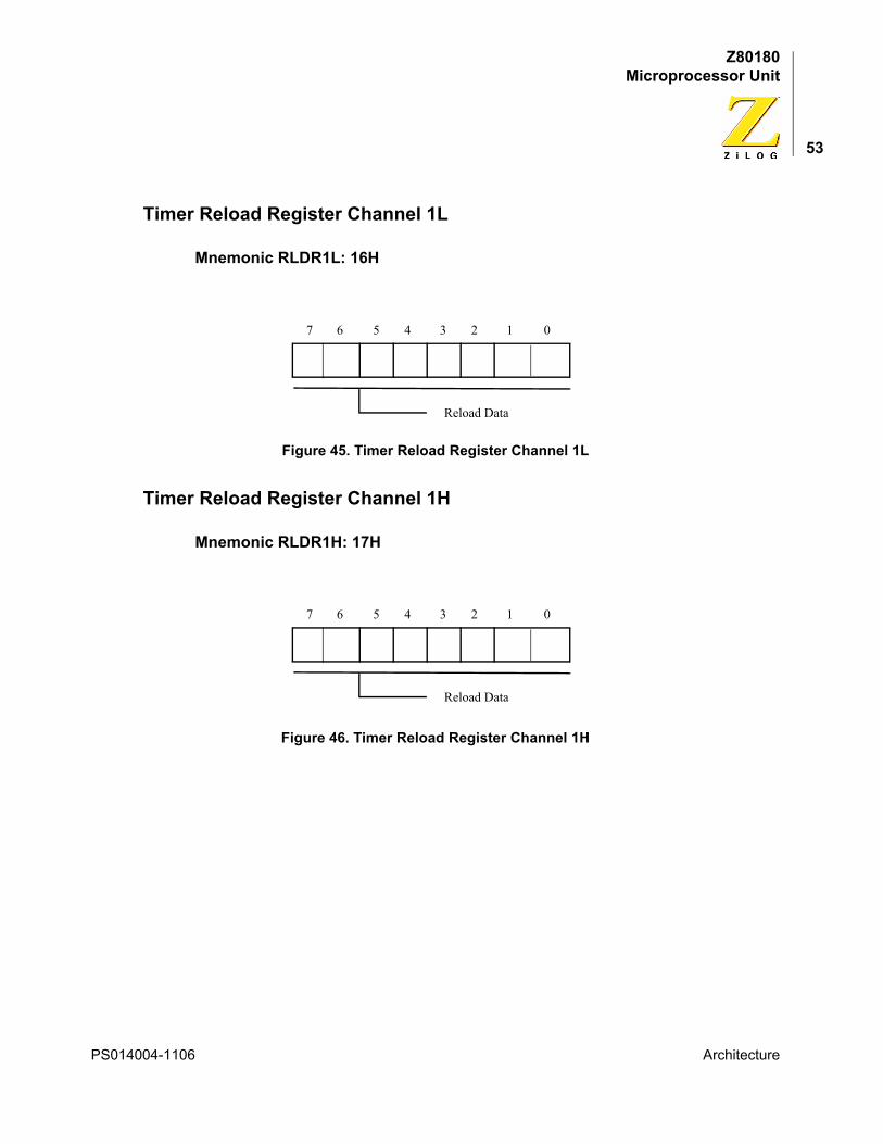
Z80180Microprocessor Unit
53
Timer Reload Register Channel 1L
Mnemonic RLDR1L: 16H
Figure 45. Timer Reload Register Channel 1L
Timer Reload Register Channel 1H
Mnemonic RLDR1H: 17H
Figure 46. Timer Reload Register Channel 1H
Timer Data Register
Timer Data Register
7 6 5 4 3 2 1 0
Reload Data
7 6 5 4 3 2 1 0
Reload Data
PS014004-1106 Architecture
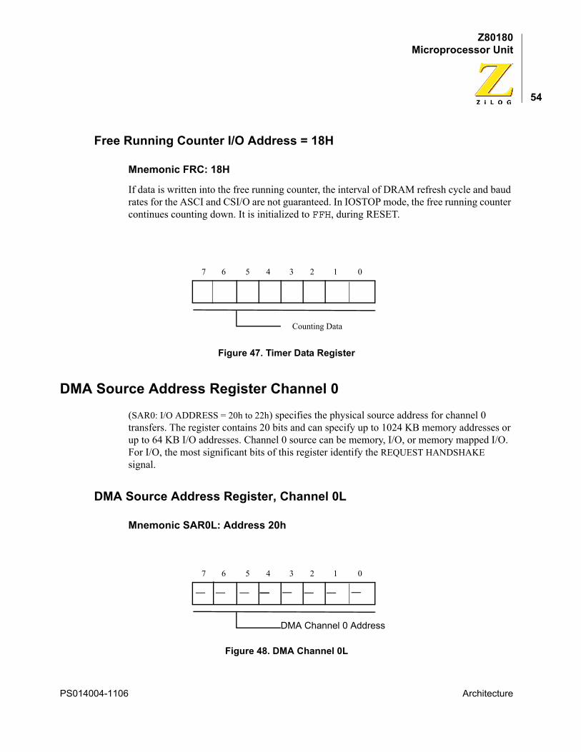
Z80180Microprocessor Unit
54
Free Running Counter I/O Address = 18H
Mnemonic FRC: 18H
If data is written into the free running counter, the interval of DRAM refresh cycle and baud rates for the ASCI and CSI/O are not guaranteed. In IOSTOP mode, the free running counter continues counting down. It is initialized to FFH, during RESET.
Figure 47. Timer Data Register
DMA Source Address Register Channel 0
(SAR0: I/O ADDRESS = 20h to 22h) specifies the physical source address for channel 0 transfers. The register contains 20 bits and can specify up to 1024 KB memory addresses or up to 64 KB I/O addresses. Channel 0 source can be memory, I/O, or memory mapped I/O. For I/O, the most significant bits of this register identify the REQUEST HANDSHAKE signal.
DMA Source Address Register, Channel 0L
Mnemonic SAR0L: Address 20h
Figure 48. DMA Channel 0L
Timer Data Register
Timer Data Register
7 6 5 4 3 2 1 0
Counting Data
DMA Channel 0 Address
— — — ——— — —
7 6 5 4 3 2 1
—
0
PS014004-1106 Architecture
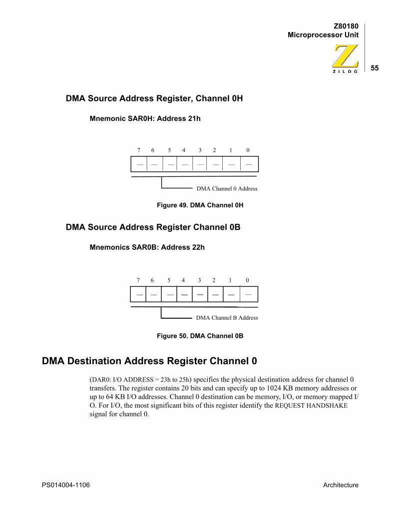
Z80180Microprocessor Unit
55
DMA Source Address Register, Channel 0H
Mnemonic SAR0H: Address 21h
Figure 49. DMA Channel 0H
DMA Source Address Register Channel 0B
Mnemonics SAR0B: Address 22h
Figure 50. DMA Channel 0B
DMA Destination Address Register Channel 0
(DAR0: I/O ADDRESS = 23h to 25h) specifies the physical destination address for channel 0 transfers. The register contains 20 bits and can specify up to 1024 KB memory addresses or up to 64 KB I/O addresses. Channel 0 destination can be memory, I/O, or memory mapped I/O. For I/O, the most significant bits of this register identify the REQUEST HANDSHAKE signal for channel 0.
Timer Data Register
Timer Data Register
DMA Channel 0 Address
— — ——— — —
7 6 5 4 3 2 1
—
0
DMA Channel B Address
— — — ——— — — — — ——— — —
7 6 5 4 3 2 1
—
0
PS014004-1106 Architecture
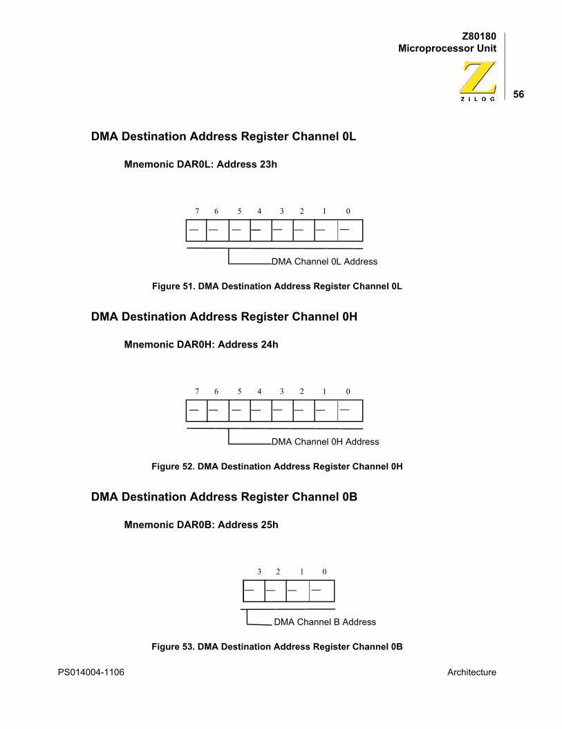
Z80180Microprocessor Unit
56
DMA Destination Address Register Channel 0L
Mnemonic DAR0L: Address 23h
Figure 51. DMA Destination Address Register Channel 0L
DMA Destination Address Register Channel 0H
Mnemonic DAR0H: Address 24h
Figure 52. DMA Destination Address Register Channel 0H
DMA Destination Address Register Channel 0B
Mnemonic DAR0B: Address 25h
Figure 53. DMA Destination Address Register Channel 0B
DMA Destination Address Register Channel 0L
DMA Destination Address Register Channel 0H
DMA Destination Address Register Channel 0B
DMA Channel 0L Address
— — — ——— — —
7 6 5 4 3 2 1
—
0
DMA Channel 0H Address
— — — ——— — —
7 6 5 4 3 2 1
—
0
DMA Channel B Address
— — —
3 2 1 0
—
PS014004-1106 Architecture
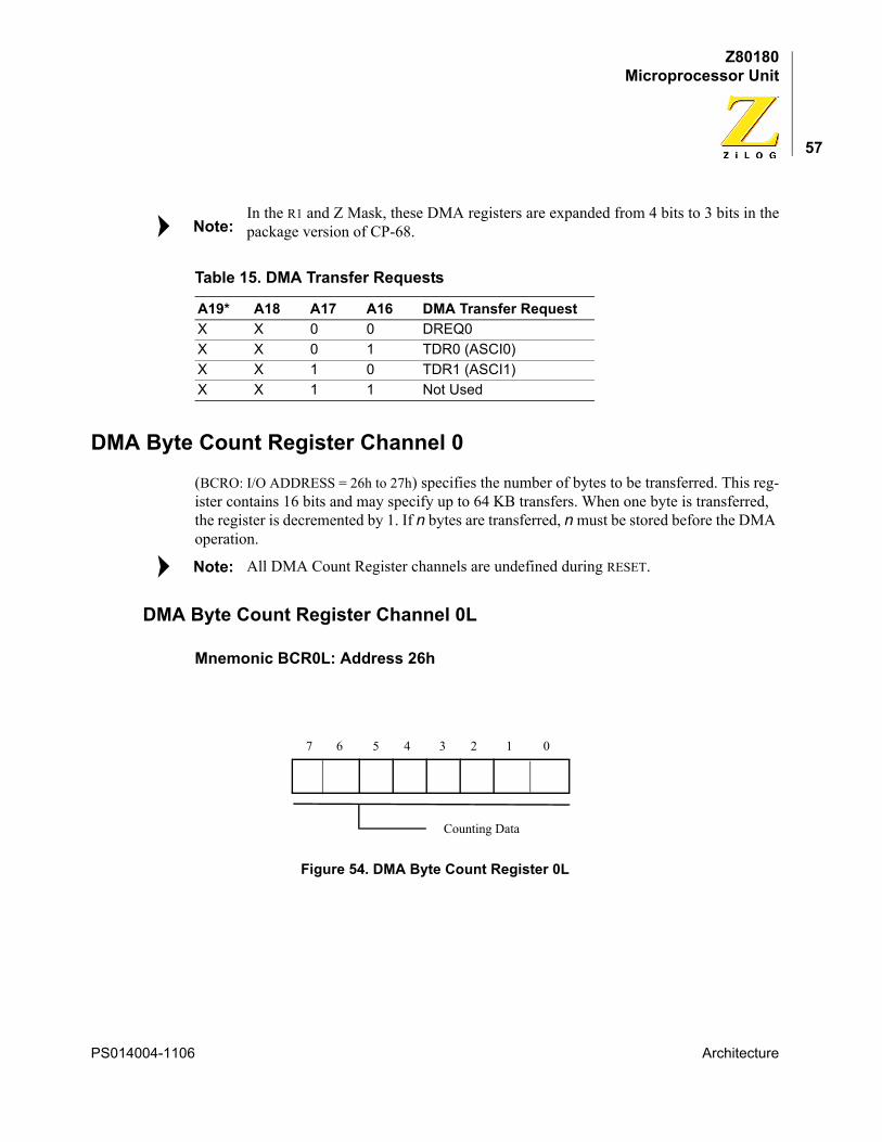
Z80180Microprocessor Unit
57
In the R1 and Z Mask, these DMA registers are expanded from 4 bits to 3 bits in thepackage version of CP-68.
DMA Byte Count Register Channel 0
(BCRO: I/O ADDRESS = 26h to 27h) specifies the number of bytes to be transferred. This reg-ister contains 16 bits and may specify up to 64 KB transfers. When one byte is transferred, the register is decremented by 1. If n bytes are transferred, n must be stored before the DMA operation.
All DMA Count Register channels are undefined during RESET.
DMA Byte Count Register Channel 0L
Mnemonic BCR0L: Address 26h
Figure 54. DMA Byte Count Register 0L
Table 15. DMA Transfer Requests
A19* A18 A17 A16 DMA Transfer Request X X 0 0 DREQ0X X 0 1 TDR0 (ASCI0)X X 1 0 TDR1 (ASCI1)X X 1 1 Not Used
DMA Byte Count Register
Note:
Note:
7 6 5 4 3 2 1 0
Counting Data
PS014004-1106 Architecture
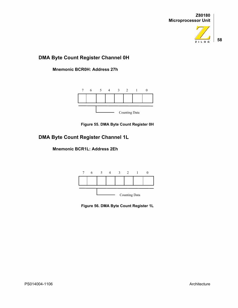
Z80180Microprocessor Unit
58
DMA Byte Count Register Channel 0H
Mnemonic BCR0H: Address 27h
Figure 55. DMA Byte Count Register 0H
DMA Byte Count Register Channel 1L
Mnemonic BCR1L: Address 2Eh
Figure 56. DMA Byte Count Register 1L
DMA Byte Count Register 0H
DMA Byte Count Register 1L
7 6 5 4 3 2 1 0
Counting Data
7 6 5 4 3 2 1 0
Counting Data
PS014004-1106 Architecture
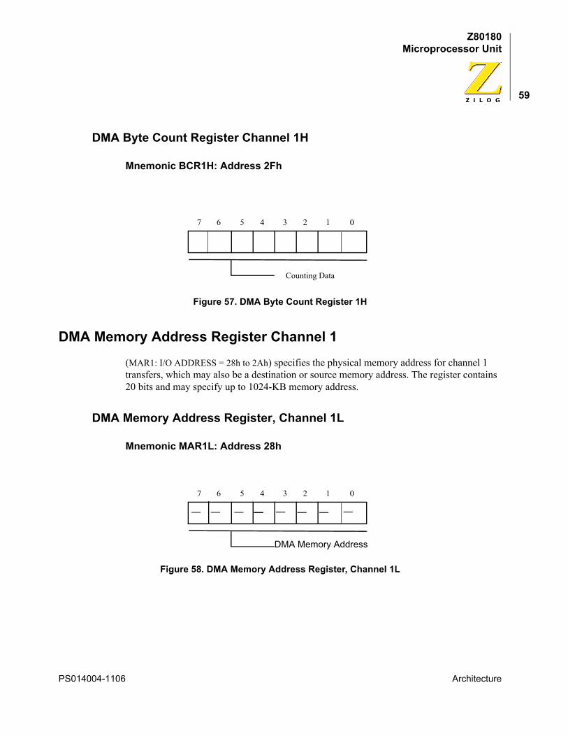
Z80180Microprocessor Unit
59
DMA Byte Count Register Channel 1H
Mnemonic BCR1H: Address 2Fh
Figure 57. DMA Byte Count Register 1H
DMA Memory Address Register Channel 1
(MAR1: I/O ADDRESS = 28h to 2Ah) specifies the physical memory address for channel 1 transfers, which may also be a destination or source memory address. The register contains 20 bits and may specify up to 1024-KB memory address.
DMA Memory Address Register, Channel 1L
Mnemonic MAR1L: Address 28h
Figure 58. DMA Memory Address Register, Channel 1L
DMA Byte Count Register 0H
DMA Memory Address Register, Channel 1L
7 6 5 4 3 2 1 0
Counting Data
DMA Memory Address
— — — ——— — —
7 6 5 4 3 2 1
—
0
PS014004-1106 Architecture
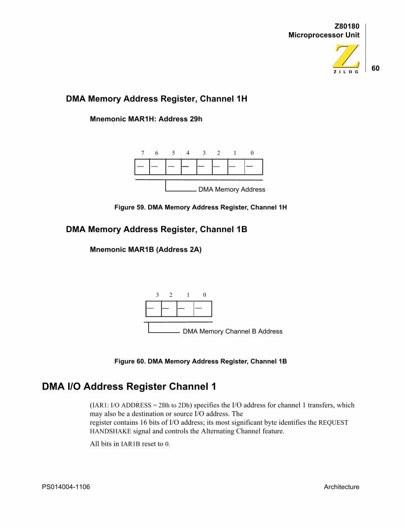
Z80180Microprocessor Unit
60
DMA Memory Address Register, Channel 1H
Mnemonic MAR1H: Address 29h
Figure 59. DMA Memory Address Register, Channel 1H
DMA Memory Address Register, Channel 1B
Mnemonic MAR1B (Address 2A)
Figure 60. DMA Memory Address Register, Channel 1B
DMA I/O Address Register Channel 1
(IAR1: I/O ADDRESS = 2Bh to 2Dh) specifies the I/O address for channel 1 transfers, which may also be a destination or source I/O address. The register contains 16 bits of I/O address; its most significant byte identifies the REQUEST HANDSHAKE signal and controls the Alternating Channel feature.
All bits in IAR1B reset to 0.
DMA Memory Address Register, Channel 1H
DMA
DMA Memory Address
— — — ——— — —
7 6 5 4 3 2 1
—
0
DMA Memory Channel B Address
— — —
3 2 1 0
—
PS014004-1106 Architecture
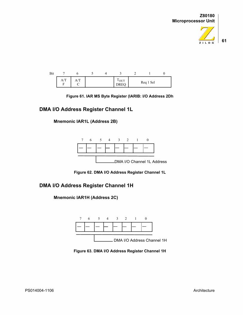
Z80180Microprocessor Unit
61
Figure 61. IAR MS Byte Register (IARIB: I/O Address 2Dh
DMA I/O Address Register Channel 1L
Mnemonic IAR1L (Address 2B)
Figure 62. DMA I/O Address Register Channel 1L
DMA I/O Address Register Channel 1H
Mnemonic IAR1H (Address 2C)
Figure 63. DMA I/O Address Register Channel 1H
IAR MS Byte Register (IARIB: I/O Address 2Dh)
DMA I/O Address Register Channel 1L
DMA I/O Address Register Channel 1H
Bit
A/T A/T
7 6 5 4 3 2 1 0
F CTOUTDREQ Req 1 Sel
DMA I/O Channel 1L Address
— — — ——— — —
7 6 5 4 3 2 1
—
0
DMA I/O Address Channel 1H
— — — ——— — —
7 6 5 4 3 2 1
—
0
PS014004-1106 Architecture
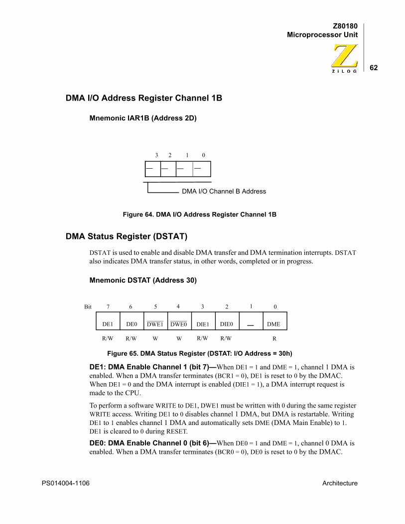
Z80180Microprocessor Unit
62
DMA I/O Address Register Channel 1B
Mnemonic IAR1B (Address 2D)
Figure 64. DMA I/O Address Register Channel 1B
DMA Status Register (DSTAT)
DSTAT is used to enable and disable DMA transfer and DMA termination interrupts. DSTAT also indicates DMA transfer status, in other words, completed or in progress.
Mnemonic DSTAT (Address 30)
Figure 65. DMA Status Register (DSTAT: I/O Address = 30h)
DE1: DMA Enable Channel 1 (bit 7)—When DE1 = 1 and DME = 1, channel 1 DMA is enabled. When a DMA transfer terminates (BCR1 = 0), DE1 is reset to 0 by the DMAC. When DE1 = 0 and the DMA interrupt is enabled (DIE1 = 1), a DMA interrupt request is made to the CPU.
To perform a software WRITE to DE1, DWE1 must be written with 0 during the same register WRITE access. Writing DE1 to 0 disables channel 1 DMA, but DMA is restartable. Writing DE1 to 1 enables channel 1 DMA and automatically sets DME (DMA Main Enable) to 1. DE1 is cleared to 0 during RESET.DE0: DMA Enable Channel 0 (bit 6)—When DE0 = 1 and DME = 1, channel 0 DMA is enabled. When a DMA transfer terminates (BCR0 = 0), DE0 is reset to 0 by the DMAC.
DMA I/O Address Register Channel 1B
DMA Status Register (DSTAT: I/O Address = 30h)
DMA I/O Channel B Address
— — —
3 2 1 0
—
Bit
DE1 DE0 DWE1
7 6 5 4 3 2 1 0
R/W R/W W
DWE0 DIE1 DIE0 DME
W R/W R/W R
PS014004-1106 Architecture
Z80180Microprocessor Unit
63
When DE0 = 0 and the DMA interrupt is enabled (DIE0 = 1), a DMA interrupt request is made to the CPU.
To perform a software WRITE to DE0, DWE0 must be written with 0 during the same register WRITE access. Writing DE0 to 0 disables channel 0 DMA. Writing DE0 to 1 enables channel 0 DMA and automatically sets DME (DMA Main Enable) to 1. DE0 is cleared to 0 during RESET.DWE1: DE1 Bit WRITE Enable (bit 5)—When performing any software WRITE to DE1, DWE1 must be written with 0 during the same access. DWE1 always reads as 1.DWE0: DE0 Bit WRITE Enable (bit 4)—When performing any software WRITE to DE0, DWE0 must be written with 0 during the same access. DWE0 always reads as 1.DIE1: DMA Interrupt Enable Channel 1 (bit 3)—When DIE0 is set to 1, the termination channel 1 DMA transfer (indicated when DE1 = 0) causes a CPU interrupt request to be generated. When DIE0 = 0, the channel 0 DMA termination interrupt is disabled. DIE0 is cleared to 0 during RESET.DIE0: DMA Interrupt Enable Channel 0 (bit 2)—When DIE0 is set to 1, the termination channel 0 of DMA transfer (indicated when DE0 = 0) causes a CPU interrupt request to be generated. When DIE0 = 0, the channel 0 DMA termination interrupt is dis-abled. DIE0 is cleared to 0 during RESET.DME: DMA Main Enable (bit 0)—A DMA operation is only enabled when its DE bit (DE0 for channel 0, DE1 for channel 1) and the DME bit is set to 1.
When NMI occurs, DME is reset to 0, disabling DMA activity during the NMI interrupt service routine. To restart DMA, DE– and/or DE1 must be written with a 1 (even if the contents are already 1). This WRITE automatically sets DME to 1, allowing DMA operations to continue.
DME cannot be directly written. It is cleared to 0 by NMI or indirectly set to 1 bysetting DE0 and/or DE1 to 1. DME is cleared to 0 during RESET.
DMA Mode Register (DMODE)
DMODE is used to set the addressing and transfer mode for channel 0.
Note:
PS014004-1106 Architecture
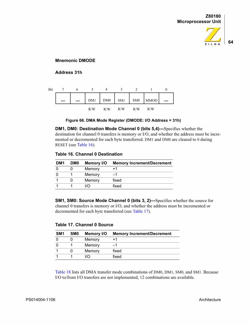
Z80180Microprocessor Unit
64
Mnemonic DMODE
Address 31h
Figure 66. DMA Mode Register (DMODE: I/O Address = 31h)
DM1, DM0: Destination Mode Channel 0 (bits 5,4)—Specifies whether the destination for channel 0 transfers is memory or I/O, and whether the address must be incre-mented or decremented for each byte transferred. DM1 and DM0 are cleared to 0 during RESET (see Table 16).
SM1, SM0: Source Mode Channel 0 (bits 3, 2)—Specifies whether the source for channel 0 transfers is memory or I/O, and whether the address must be incremented or decremented for each byte transferred (see Table 17).
Table 18 lists all DMA transfer mode combinations of DM0, DM1, SM0, and SM1. Because I/O to/from I/O transfers are not implemented, 12 combinations are available.
DMA Mode Register (DMODE: I/O Address = 31h)
Table 16. Channel 0 Destination
DM1 DM0 Memory I/O Memory Increment/Decrement0 0 Memory +10 1 Memory –11 0 Memory fixed1 1 I/O fixed
Table 17. Channel 0 Source
SM1 SM0 Memory I/O Memory Increment/Decrement0 0 Memory +10 1 Memory –11 0 Memory fixed1 1 I/O fixed
Bit
DM1 DM0
7 6 5 4 3 2 1 0
R/W R/W
SM1 SM0 MMOD
R/W R/W R/W
PS014004-1106 Architecture
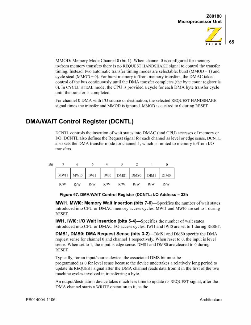
Z80180Microprocessor Unit
65
MMOD: Memory Mode Channel 0 (bit 1). When channel 0 is configured for memory to/from memory transfers there is no REQUEST HANDSHAKE signal to control the transfer timing. Instead, two automatic transfer timing modes are selectable: burst (MMOD = 1) and cycle steal (MMOD = 0). For burst memory to/from memory transfers, the DMAC takes control of the bus continuously until the DMA transfer completes (the byte count register is 0). In CYCLE STEAL mode, the CPU is provided a cycle for each DMA byte transfer cycle until the transfer is completed.
For channel 0 DMA with I/O source or destination, the selected REQUEST HANDSHAKE signal times the transfer and MMOD is ignored. MMOD is cleared to 0 during RESET.
DMA/WAIT Control Register (DCNTL)
DCNTL controls the insertion of wait states into DMAC (and CPU) accesses of memory or I/O. DCNTL also defines the Request signal for each channel as level or edge sense. DCNTL also sets the DMA transfer mode for channel 1, which is limited to memory to/from I/O transfers.
Figure 67. DMA/WAIT Control Register (DCNTL: I/O Address = 32h
MWI1, MWI0: Memory Wait Insertion (bits 7-6)—Specifies the number of wait states introduced into CPU or DMAC memory access cycles. MWI1 and MWI0 are set to 1 during RESET.IWI1, IWI0: I/O Wait Insertion (bits 5-4)—Specifies the number of wait states introduced into CPU or DMAC I/O access cycles. IWI1 and IWI0 are set to 1 during RESET.DMS1, DMS0: DMA Request Sense (bits 3-2)—DMS1 and DMS0 specify the DMA request sense for channel 0 and channel 1 respectively. When reset to 0, the input is level sense. When set to 1, the input is edge sense. DMS1 and DMS0 are cleared to 0 during RESET.
Typically, for an input/source device, the associated DMS bit must be programmed as 0 for level sense because the device undertakes a relatively long period to update its REQUEST signal after the DMA channel reads data from it in the first of the two machine cycles involved in transferring a byte.
An output/destination device takes much less time to update its REQUEST signal, after the DMA channel starts a WRITE operation to it, as the
DMA/WAIT Control Register (DCNTL: I/O Address = 32h)
Bit
MWI1 IWI0
7 6 5 4 3 2 1 0
R/W R/W
DMS1 DMS0 DIM1
R/W R/W R/W
MWI0 IWI1 DIM0
R/W R/W R/W
PS014004-1106 Architecture
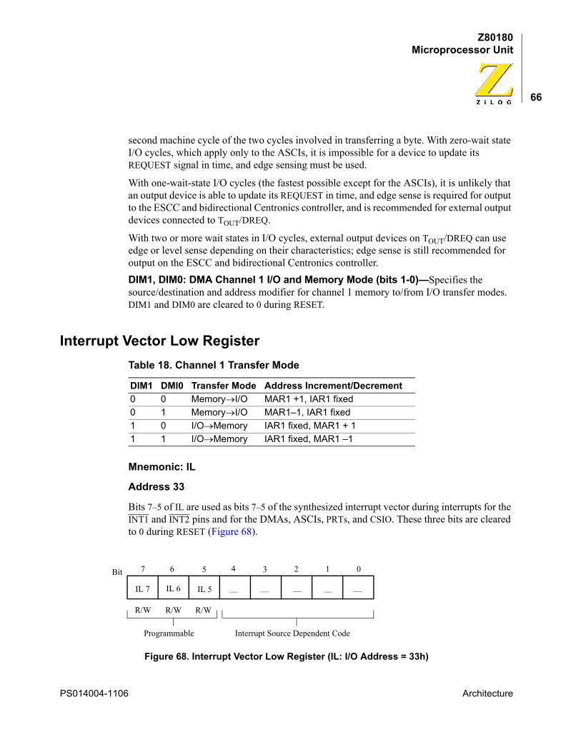
Z80180Microprocessor Unit
66
second machine cycle of the two cycles involved in transferring a byte. With zero-wait state I/O cycles, which apply only to the ASCIs, it is impossible for a device to update its REQUEST signal in time, and edge sensing must be used.
With one-wait-state I/O cycles (the fastest possible except for the ASCIs), it is unlikely that an output device is able to update its REQUEST in time, and edge sense is required for output to the ESCC and bidirectional Centronics controller, and is recommended for external output devices connected to TOUT/DREQ.
With two or more wait states in I/O cycles, external output devices on TOUT/DREQ can use edge or level sense depending on their characteristics; edge sense is still recommended for output on the ESCC and bidirectional Centronics controller.DIM1, DIM0: DMA Channel 1 I/O and Memory Mode (bits 1-0)—Specifies the source/destination and address modifier for channel 1 memory to/from I/O transfer modes. DIM1 and DIM0 are cleared to 0 during RESET.
Interrupt Vector Low Register
Mnemonic: IL
Address 33
Bits 7–5 of IL are used as bits 7–5 of the synthesized interrupt vector during interrupts for the INT1 and INT2 pins and for the DMAs, ASCIs, PRTs, and CSIO. These three bits are cleared to 0 during RESET (Figure 68).
Figure 68. Interrupt Vector Low Register (IL: I/O Address = 33h)
Table 18. Channel 1 Transfer Mode
DIM1 DMI0 Transfer Mode Address Increment/Decrement0 0 Memory→I/O MAR1 +1, IAR1 fixed0 1 Memory→I/O MAR1–1, IAR1 fixed1 0 I/O→Memory IAR1 fixed, MAR1 + 11 1 I/O→Memory IAR1 fixed, MAR1 –1
Interrupt Vector Low Register (IL: I/O Address = 33h)
Bit
IL 7 IL 6
Interrupt Source Dependent Code
IL 5
7 6 5 4 3 2 1 0
–– ––
R/W R/W
–– –– ––
R/W
Programmable
PS014004-1106 Architecture
Z80180Microprocessor Unit
67
Int/TRAP Control Register
Mnemonics ITC
Address 34
INT/TRAP Control Register (ITC, I/O Address 34h)
This register is used in handling TRAP interrupts and to enable or disable Maskable Interrupt Level 0 and the INT1 and INT2 pins.
Figure 69. Int/TRAP Control Register
TRAP (bit 7)—This bit is set to 1 when an undefined opcode is fetched. TRAP can be reset under program control by writing it with a 0, however, it cannot be written with 1 under pro-gram control. TRAP is reset to 0 during RESET.UFO: Undefined Fetch Object (bit 6)—When a TRAP interrupt occurs, the contents of a UFO allow the starting address of the undefined instruction to be determined. However, the TRAP may occur on either the second or third byte of the opcode. A UFO allows the stacked Program Counter (PC) value to be correctly adjusted. If UFO = 0, the first opcode must be interpreted as the stacked PC-1. If UFO = 1, the first opcode address is stacked PC-2. UFO is READ-ONLY.ITE2, 1, 0: Interrupt Enable 2, 1, 0 (bits 2-0)—ITE2 and ITE1 enable and disable the external interrupt inputs INT2 and INT1, respectively. ITE0 enables and disables interrupts from the on-chip ESCC, CTCs and bidirectional Centronics controller as well as the external interrupt input INT0. A 1 in a bit enables the corresponding interrupt level while a 0 disables it. A RESET clears ITE0 to 1 and clears ITE1 and ITE2 to 0.
TRAP InterruptThe Z80180 generates a nonmaskable (not affected by the state of IEF1) TRAP interrupt when an undefined opcode fetch occurs. This feature can be used to increase software reli-ability, implement an extended instruction set, or both. TRAP may occur during opcode fetch cycles and also if an undefined opcode is fetched during the interrupt acknowledge cycle for INT0 when Mode 0 is used.
Bit
TRAP UFO
R/W R/W R/W
––
7 6 5 4 3 2 1 0
–– –– ITE2 ITE1 ITE0
R/W R
PS014004-1106 Architecture
Z80180Microprocessor Unit
68
When a TRAP interrupt occurs, the Z80180 operates as follows:
1. The TRAP bit in the Interrupt TRAP/Control (ITC) register is set to 1.
2. The current Program Counter (PC) value, reflecting the location of the undefined opcode, is saved on the stack.
3. The Z80180 vectors to logical address 0.
If logical address 0000h is mapped to physical address 00000h, the vector is thesame as for RESET. In this case, testing the TRAP bit in ITC reveals whether therestart at physical address 00000h was caused by RESET or TRAP.
All TRAP interrupts occur after fetching an undefined second opcode byte following one of the prefix opcodes CBh, DDh, EDh, or FDh, or after fetching an undefined third opcode byte following one of the double-prefix opcodes DDCBh or FDCBh.
The state of the Undefined Fetch Object (UFO) bit in ITC allows TRAP software to correctly adjust the stacked PC, depending on whether the second or third byte of the opcode gener-ated the TRAP. If UFO = 0, the starting address of the invalid instruction is equal to the stacked PC-1. If UFO = 1, the starting address of the invalid instruction is equal to the stacked PC-2.
Figure 70. TRAP Timing—2nd Opcode Undefined
TRAP Timing—2nd Op Code Undefined
Note:
T1 T2 T3 TTP Ti Ti Ti Ti Ti T1 T2 T3 T2 T3 T1T1 T2
A0–A18 (A19)
φ
D0–D7
PC 0000hSP-1
Undefined
MREQ
M1
RD
WR
T3
SP-2
Opcode
PCH PCL
2nd OpcodeFetch Cycle
PC StackingOpcodeFetch Cycle
Restart from 0000h
PS014004-1106 Architecture
Z80180Microprocessor Unit
69
Figure 71. TRAP Timing—3rd Opcode Undefined
Refresh Control Register
Mnemonic RCR (Address 36)
Figure 72. Refresh Control Register (RCA: I/O Address = 36h)
The RCR specifies the interval and length of refresh cycles, while enabling or disabling the refresh function.REFE: Refresh Enable (bit 7)— REFE = 0 disables the refresh controller, while REFE = 1 enables refresh cycle insertion. REFE is set to 1 during RESET.REFW: Refresh Wait (bit 6)—REFW = 0 causes the refresh cycle to be two clocks in duration. REFW = 1 causes the refresh cycle to be three clocks in duration by adding a refresh wait cycle (TRW). REFW is set to 1 during RESET.
TRAP Timing—3rd Op Code Undefined
Refresh Control Register (RCA: I/O Address = 36h)
T1 T2 T3 T1 T2 TTP T3 Ti Ti T1 T2 T3 T2 T3 T1T1 T2
A0–A18 (A19)
φ
D0–D7
PC 0000hSP-1
Undefined
MREQ
M1
RD
WR
T3
SP-2
Opcode
PC-1H PC-1L
3nd OpcodeFetch Cycle PC Stacking
OpcodeFetch Cycle
Restart
Memory
IX + d, IY + d
Ti Ti
READ Cycle
from 0000h
Reserved
— — — —— — —
7 6 5 4 3 2 1
Cyc1
Cyc0REFW
REFE
-
—
0
PS014004-1106 Architecture
Z80180Microprocessor Unit
70
CYC1, 0: Cycle Interval (bit 1,0)—CYC1 and CYC0 specify the interval (in clock cycles) between refresh cycles. In the case of dynamic RAMs requiring 128 refresh cycles every 2 ms (or 256 cycles in every 4 ms), the required refresh interval is less than or equal to 15.625 µs. The underlined values indicate the best refresh interval depending on CPU clock frequency. CYC0 and CYC1 are cleared to 0 during RESET (see Table 19).
Refresh Control and RESET
After RESET, based on the initialized value of RCR, refresh cycles occur with an interval of 10 clock cycles and be 3 clock cycles in duration.
Dynamic RAM Refresh Operation
1. REFRESH CYCLE insertion is stopped when the CPU is in the following states:a. During RESETb. When the bus is released in response to BUSREQ
c. During SLEEP mode
d. During WAIT states
2. Refresh cycles are suppressed when the bus is released in response to BUSREQ. However, the refresh timer continues to operate. The time at which the first refresh cycle occurs after the Z80180 reacquires the bus depends on the refresh timer, and possesses no timing relationship with the bus exchange.
3. Refresh cycles are suppressed during SLEEP mode. If a refresh cycle is requested during SLEEP mode, the refresh cycle request is internally latched (until replaced with the next refresh request). The latched refresh cycle is inserted at the end of the first machine cycle after SLEEP mode is exited. After this initial cycle, the time at which the next refresh cycle occurs depends on the refresh time and carries no relationship with the exit from SLEEP mode.
Table 19. DRAM Refresh Intervals
Insertion Interval
Time Interval
CYC1 CYC0 Ø: 10 MHz 8 MHz 6 MHz 4 MHz 2.5 MHz
0 0 10 states (1.0 µs)* (1.25 µs)* 1.66 µs 2.5 µs 4.0 µs
0 1 20 states (2.0 µs)* (2.5 µs)* 3.3 µs 5.0 µs 8.0 µs
1 0 40 states (4.0 µs)* (5.0 µs)* 6.6 µs 10.0 µs 16.0 µs
1 1 80 states (8.0 µs)* (10.0 µs)* 13.3 µs 20.0 µs 32.0 µs
*Calculated interval.
PS014004-1106 Architecture
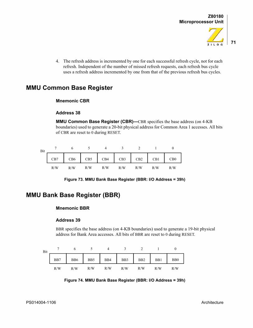
Z80180Microprocessor Unit
71
4. The refresh address is incremented by one for each successful refresh cycle, not for each refresh. Independent of the number of missed refresh requests, each refresh bus cycle uses a refresh address incremented by one from that of the previous refresh bus cycles.
MMU Common Base Register
Mnemonic CBR
Address 38
MMU Common Base Register (CBR)—CBR specifies the base address (on 4-KB boundaries) used to generate a 20-bit physical address for Common Area 1 accesses. All bits of CBR are reset to 0 during RESET.
Figure 73. MMU Bank Base Register (BBR: I/O Address = 39h)
MMU Bank Base Register (BBR)
Mnemonic BBR
Address 39
BBR specifies the base address (on 4-KB boundaries) used to generate a 19-bit physical address for Bank Area accesses. All bits of BBR are reset to 0 during RESET.
Figure 74. MMU Bank Base Register (BBR: I/O Address = 39h)
MMU Bank Base Register (BBR: I/O Address = 39h)
MMU Bank Base Register (BBR: I/O Address = 39h)
Bit
CB7 CB6
R/W
CB5
7 6 5 4 3 2 1 0
CB4 CB2 CB1 CB0
R/W
CB3
R/WR/WR/WR/WR/WR/W
Bit
BB7 BB6
R/W
BB5
7 6 5 4 3 2 1 0
BB4 BB2 BB1 BB0
R/W
BB3
R/WR/WR/WR/WR/WR/W
PS014004-1106 Architecture
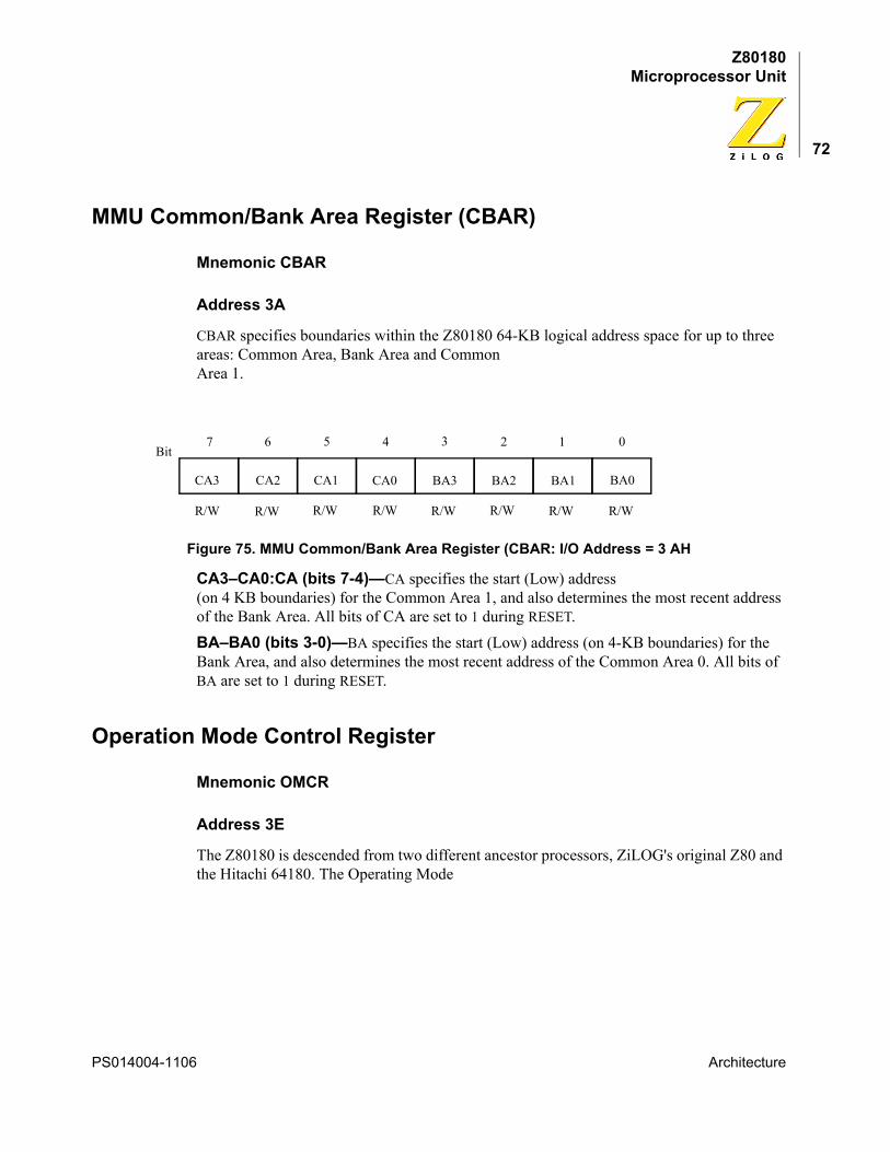
Z80180Microprocessor Unit
72
MMU Common/Bank Area Register (CBAR)
Mnemonic CBAR
Address 3A
CBAR specifies boundaries within the Z80180 64-KB logical address space for up to three areas: Common Area, Bank Area and Common Area 1.
Figure 75. MMU Common/Bank Area Register (CBAR: I/O Address = 3 AH
CA3–CA0:CA (bits 7-4)—CA specifies the start (Low) address (on 4 KB boundaries) for the Common Area 1, and also determines the most recent address of the Bank Area. All bits of CA are set to 1 during RESET.BA–BA0 (bits 3-0)—BA specifies the start (Low) address (on 4-KB boundaries) for the Bank Area, and also determines the most recent address of the Common Area 0. All bits of BA are set to 1 during RESET.
Operation Mode Control Register
Mnemonic OMCR
Address 3E
The Z80180 is descended from two different ancestor processors, ZiLOG's original Z80 and the Hitachi 64180. The Operating Mode
MMU Common/Bank Area Register (CBAR: I/O Address = 3 AH
Bit
CA3 CA2
R/W
CA1
7 6 5 4 3 2 1 0
CA0 BA2 BA1 BA0
R/W
BA3
R/WR/WR/WR/WR/WR/W
PS014004-1106 Architecture
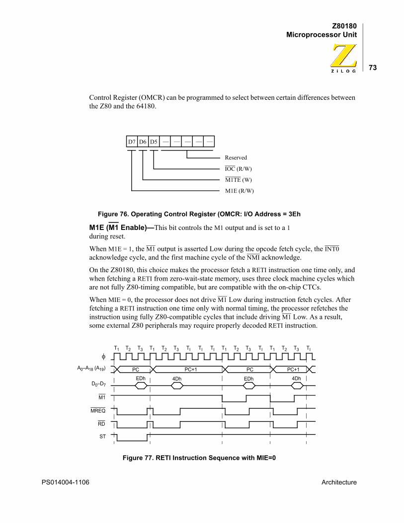
Z80180Microprocessor Unit
73
Control Register (OMCR) can be programmed to select between certain differences between the Z80 and the 64180.
Figure 76. Operating Control Register (OMCR: I/O Address = 3Eh
M1E (M1 Enable)—This bit controls the M1 output and is set to a 1 during reset.
When M1E = 1, the M1 output is asserted Low during the opcode fetch cycle, the INT0 acknowledge cycle, and the first machine cycle of the NMI acknowledge.
On the Z80180, this choice makes the processor fetch a RETI instruction one time only, and when fetching a RETI from zero-wait-state memory, uses three clock machine cycles which are not fully Z80-timing compatible, but are compatible with the on-chip CTCs.
When MIE = 0, the processor does not drive M1 Low during instruction fetch cycles. After fetching a RETI instruction one time only with normal timing, the processor refetches the instruction using fully Z80-compatible cycles that include driving M1 Low. As a result, some external Z80 peripherals may require properly decoded RETI instruction.
Figure 77. RETI Instruction Sequence with MIE=0
Operating Control OMCR: I/O Address = 3Eh)
D7
Reserved
D6 D5 —
IOC (R/W)
M1TE (W)
M1E (R/W)
— — — —
T1 T2 T3 T1 T2 T3 TI TI TI T1 T2 T3 T1 T2 T3TI TI
A0–A18 (A19)
φ
D0–D7
PC PC+1 PC PC+1EDh 4Dh EDh 4Dh
MREQ
M1
RD
ST
PS014004-1106 Architecture
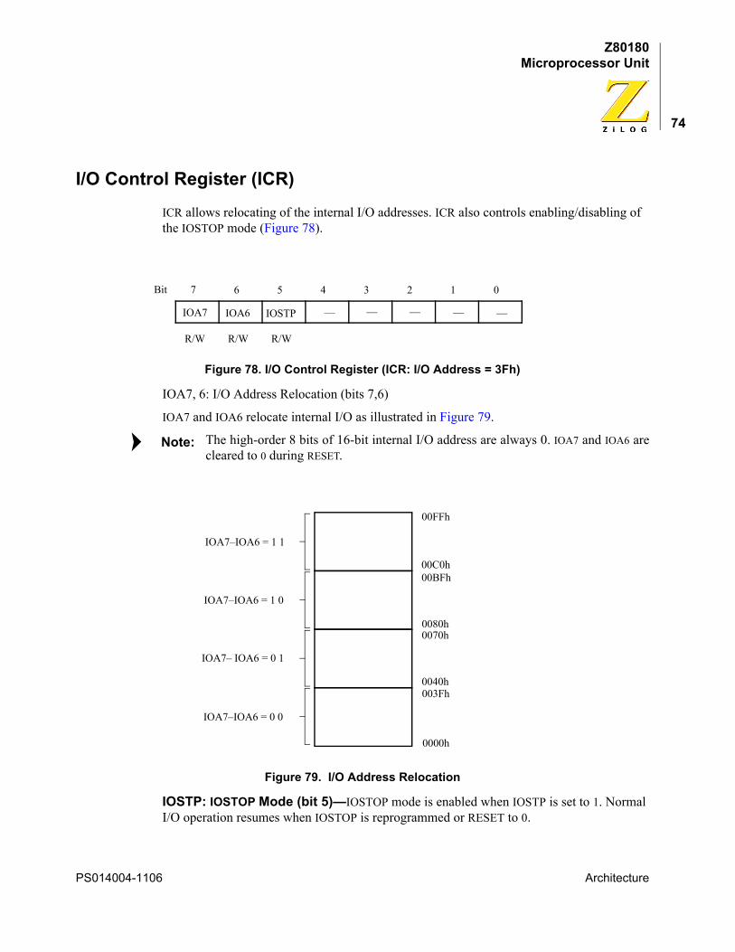
Z80180Microprocessor Unit
74
I/O Control Register (ICR)
ICR allows relocating of the internal I/O addresses. ICR also controls enabling/disabling of the IOSTOP mode (Figure 78).
Figure 78. I/O Control Register (ICR: I/O Address = 3Fh)
IOA7, 6: I/O Address Relocation (bits 7,6)
IOA7 and IOA6 relocate internal I/O as illustrated in Figure 79.
The high-order 8 bits of 16-bit internal I/O address are always 0. IOA7 and IOA6 arecleared to 0 during RESET.
Figure 79. I/O Address Relocation
IOSTP: IOSTOP Mode (bit 5)—IOSTOP mode is enabled when IOSTP is set to 1. Normal I/O operation resumes when IOSTOP is reprogrammed or RESET to 0.
I/O Control Register (ICR: I/O Address = 3Fh)
IOA7 IOA6 —— — —IOSTP
Bit 7 6 5 4 3 2 1 0
—
R/W R/W R/W
Note:
IOA7–IOA6 = 1 1
IOA7–IOA6 = 1 0
IOA7– IOA6 = 0 1
IOA7–IOA6 = 0 0
00FFh
00C0h00BFh
0080h0070h
0040h003Fh
0000h
PS014004-1106 Architecture
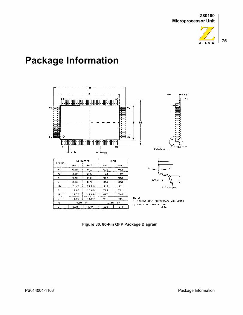
Z80180Microprocessor Unit
75
Package Information
Figure 80. 80-Pin QFP Package Diagram
PS014004-1106 Package Information
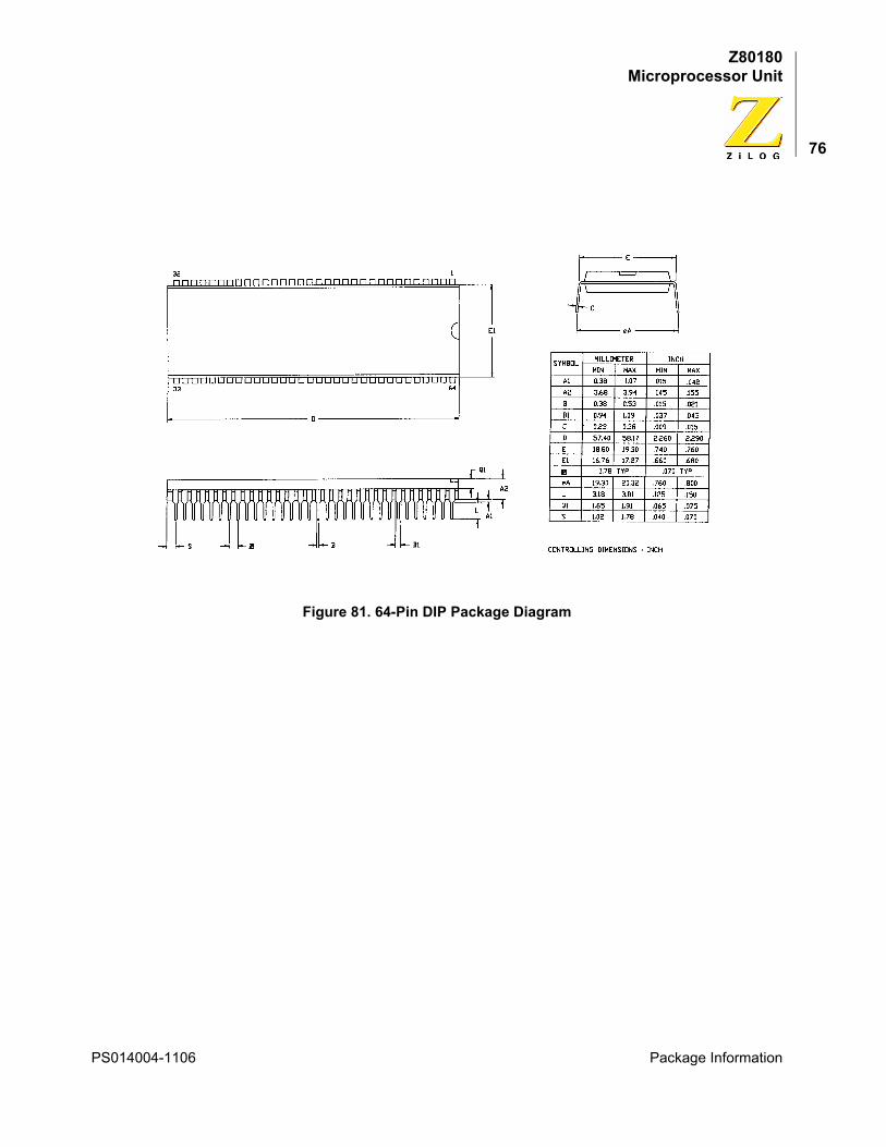
Z80180Microprocessor Unit
76
Figure 81. 64-Pin DIP Package Diagram
PS014004-1106 Package Information
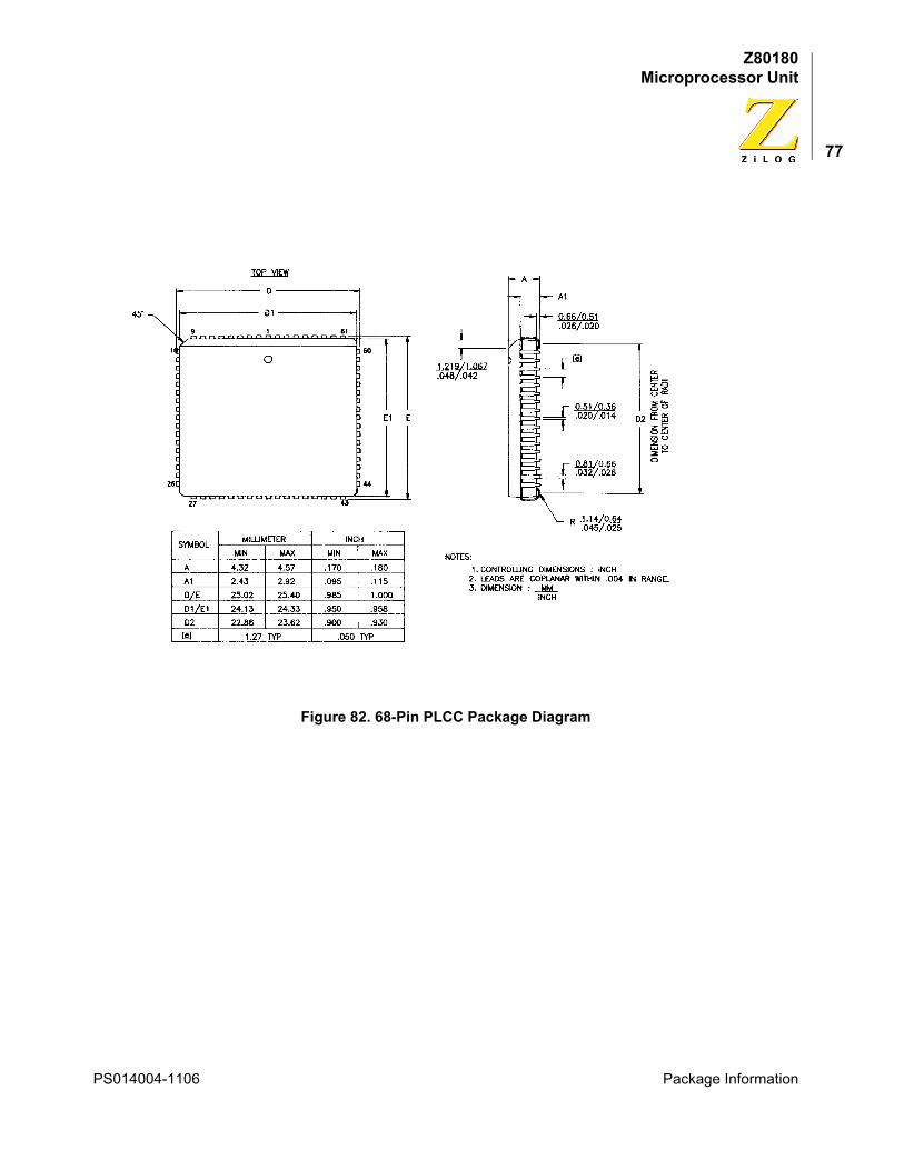
Z80180Microprocessor Unit
77
Figure 82. 68-Pin PLCC Package Diagram
68-Pin PLCC Package Diagram
PS014004-1106 Package Information
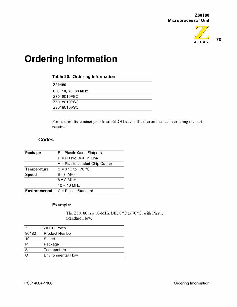
Z80180Microprocessor Unit
78
Ordering Information
For fast results, contact your local ZiLOG sales office for assistance in ordering the part required.
Codes
Example:
The Z80180 is a 10-MHz DIP, 0 ºC to 70 ºC, with Plastic Standard Flow.
Table 20. Ordering Information
Z801806, 8, 10, 20, 33 MHzZ8018010FSCZ8018010PSCZ8018010VSC
Package F = Plastic Quad FlatpackP = Plastic Dual In LineV = Plastic Leaded Chip Carrier
Temperature S = 0 °C to +70 °CSpeed 6 = 6 MHz
8 = 8 MHz10 = 10 MHz
Environmental C = Plastic Standard
Z ZiLOG Prefix80180 Product Number10 SpeedP PackageS TemperatureC Environmental Flow
PS014004-1106 Ordering Information
PS014004-1106 Customer Support
Z80180Microprocessor Unit
79
Customer SupportIf you experience any problems while operating this product, please check the ZiLOG Knowledge Base:
http://kb.zilog.com/kb/oKBmain.asp
If you cannot find an answer or have further questions, please see the ZiLOG Technical Support web page:
http://support.zilog.com