Embed Size (px)
Citation preview
Microprocessors and Microcontrollers
(EE-231)
Main Objectives
• 8088 and 80188 8-bit Memory Interface • 8086 t0 80386SX 16-bit Memory Interface • I/O Interfacing
– I/O Address Decoding
More on Address Decoding
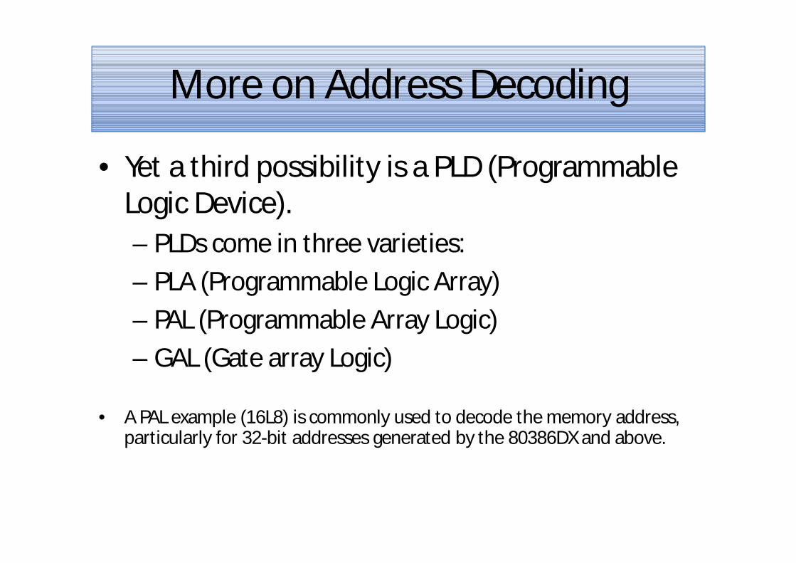
• Yet a third possibility is a PLD (Programmable Logic Device). – PLDs come in three varieties: – PLA (Programmable Logic Array) – PAL (Programmable Array Logic) – GAL (Gate array Logic)
• A PAL example (16L8) is commonly used to decode the memory address,
particularly for 32-bit addresses generated by the 80386DX and above.
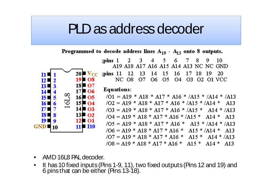
PLD as address decoder
• AMD 16L8 PAL decoder. • It has 10 fixed inputs (Pins 1-9, 11), two fixed outputs (Pins 12 and 19) and
6 pins that can be either (Pins 13-18).
• 8088/80188 microprocessors have an 8-bit data bus, which makes them ideal to connect to common 8-bit memory devices available.
• For the 8088/80188 to function correctly with memory, however, the system must decode the address to select a memory component.
Basic 8088/80188 Memory Interface
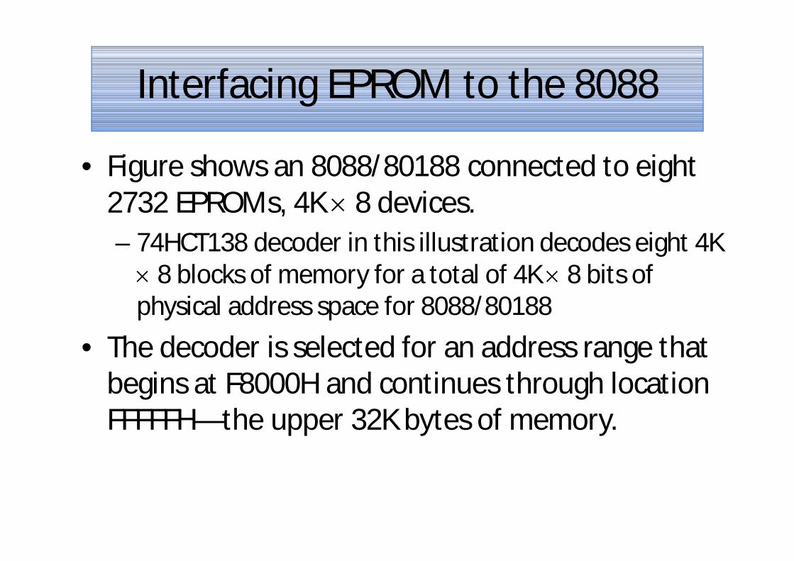
• Figure shows an 8088/80188 connected to eight 2732 EPROMs, 4K 8 devices. – 74HCT138 decoder in this illustration decodes eight 4K 8 blocks of memory for a total of 4K 8 bits of physical address space for 8088/80188
• The decoder is selected for an address range that begins at F8000H and continues through location FFFFFH—the upper 32K bytes of memory.
Interfacing EPROM to the 8088
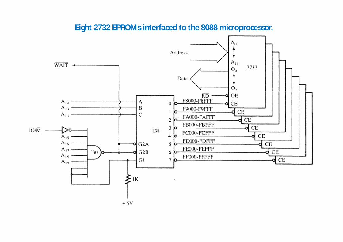
Eight 2732 EPROMs interfaced to the 8088 microprocessor.
• This section of memory is an EPROM because FFFF0H is where the 8088 starts to execute instructions after a hardware reset. – often called the cold-start location
• The software stored in this section of memory would contain a JMP instruction at location FFFF0H that jumps from this location – so the remainder of the program can execute
Interfacing EPROM to the 8088
• RAM is easier to interface than EPROM as most RAM does not require wait states. – The very bottom section of RAM contains vectors for
interrupts
• Figure shows sixteen 62256 static RAMs interfaced to the 8088, beginning at 00000H.
Interfacing RAM to the 8088
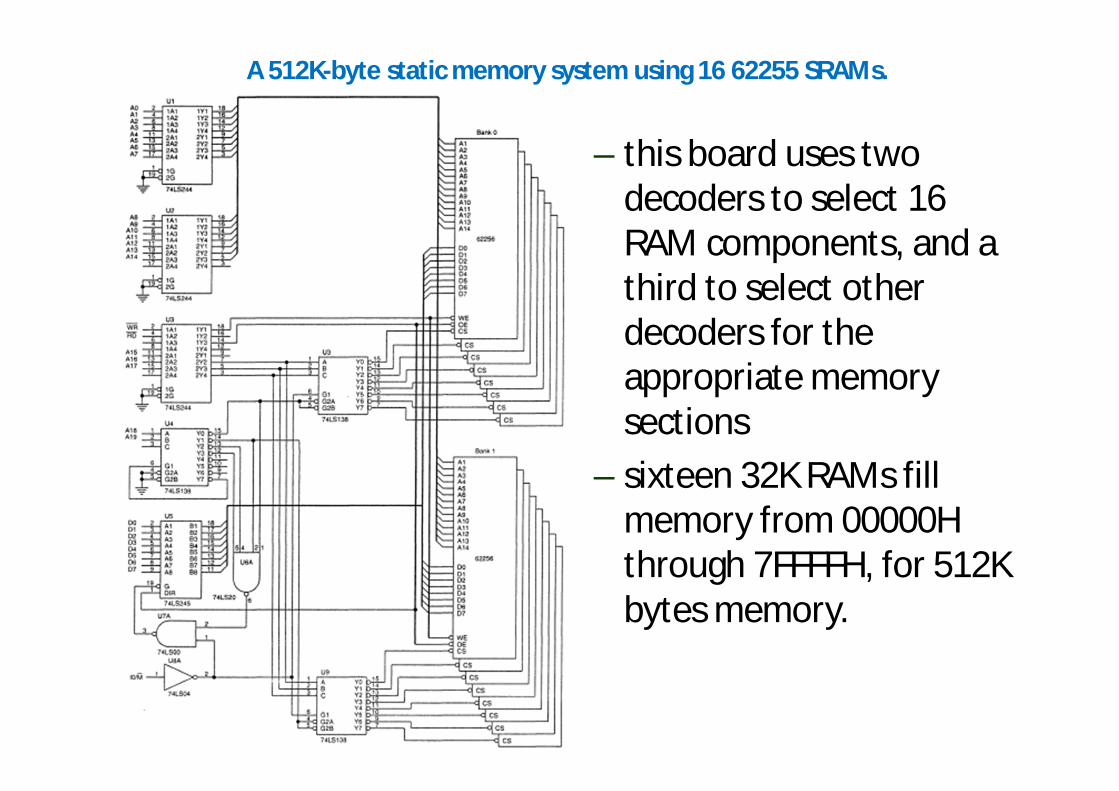
A 512K-byte static memory system using 16 62255 SRAMs.
– this board uses two decoders to select 16 RAM components, and a third to select other decoders for the appropriate memory sections
– sixteen 32K RAMs fill memory from 00000H through 7FFFFH, for 512K bytes memory.
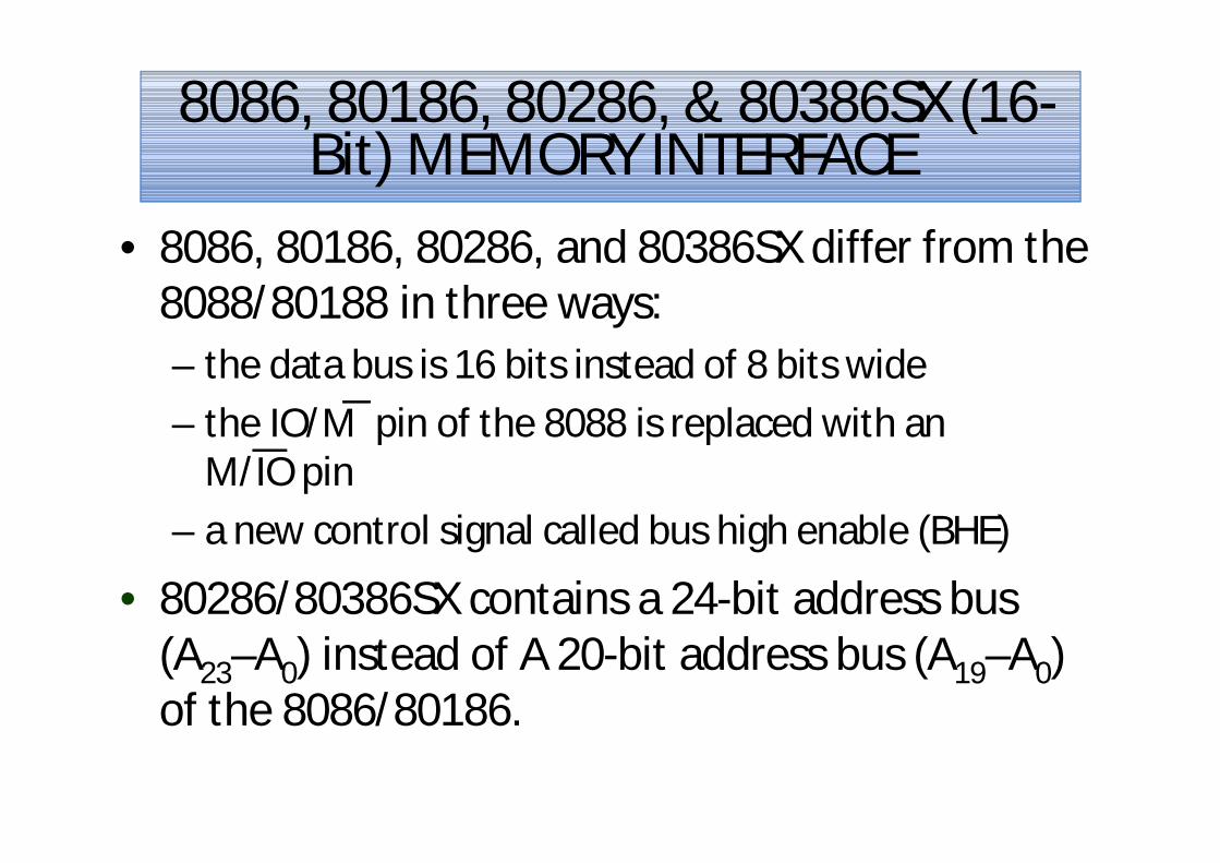
• 8086, 80186, 80286, and 80386SX differ from the 8088/80188 in three ways: – the data bus is 16 bits instead of 8 bits wide – the IO/M pin of the 8088 is replaced with an
M/IO pin – a new control signal called bus high enable (BHE)
• 80286/80386SX contains a 24-bit address bus (A23–A0) instead of A 20-bit address bus (A19–A0) of the 8086/80186.
8086, 80186, 80286, & 80386SX (16-
8086, 80186, 80286, & 80386SX (16-Bit) MEMORY INTERFACE
• The data bus of 8086, 80186, 80286, and 80386SX is twice as wide as for the 8088/80188. – the wider bus presents a unique set of problems – processors must be able to write data to any
16-bit location—or any 8-bit location
• This means the 16-bit data bus must be divided into two separate sections (or banks) 8 bits wide so that the processor can write to either half (8-bit) or both halves (16-bit).
16-Bit Bus Control
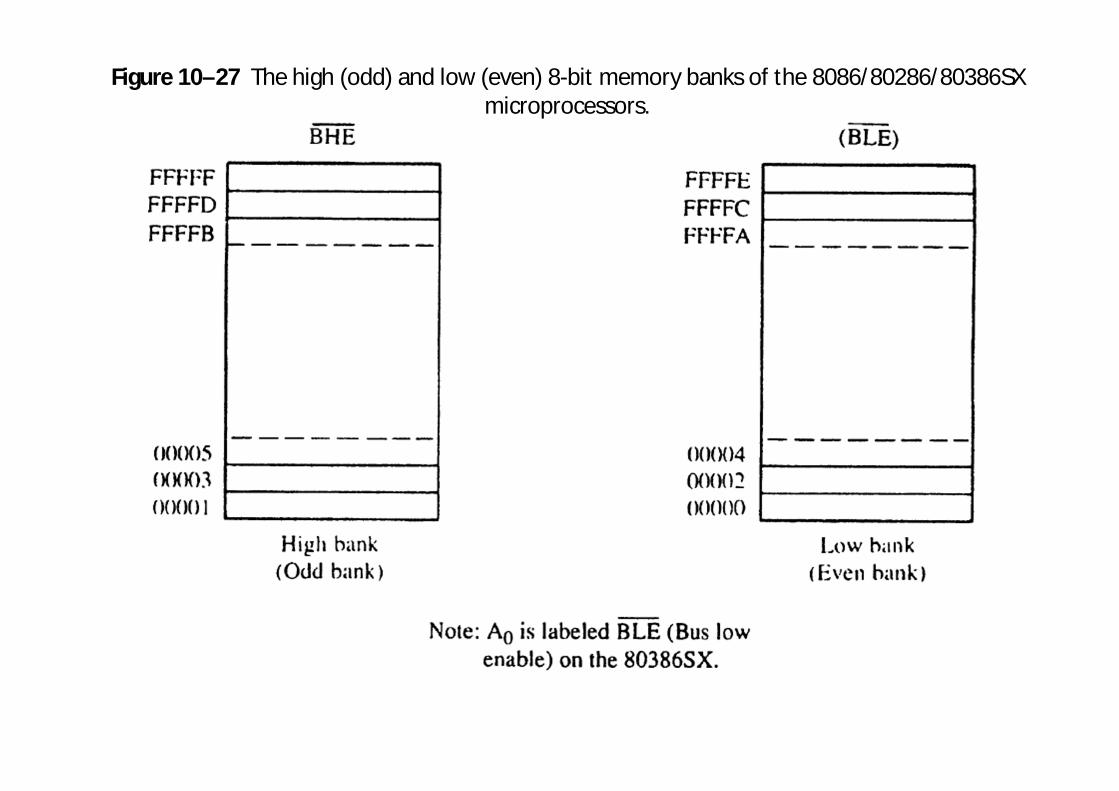
Figure 10–27 The high (odd) and low (even) 8-bit memory banks of the 8086/80286/80386SX microprocessors.
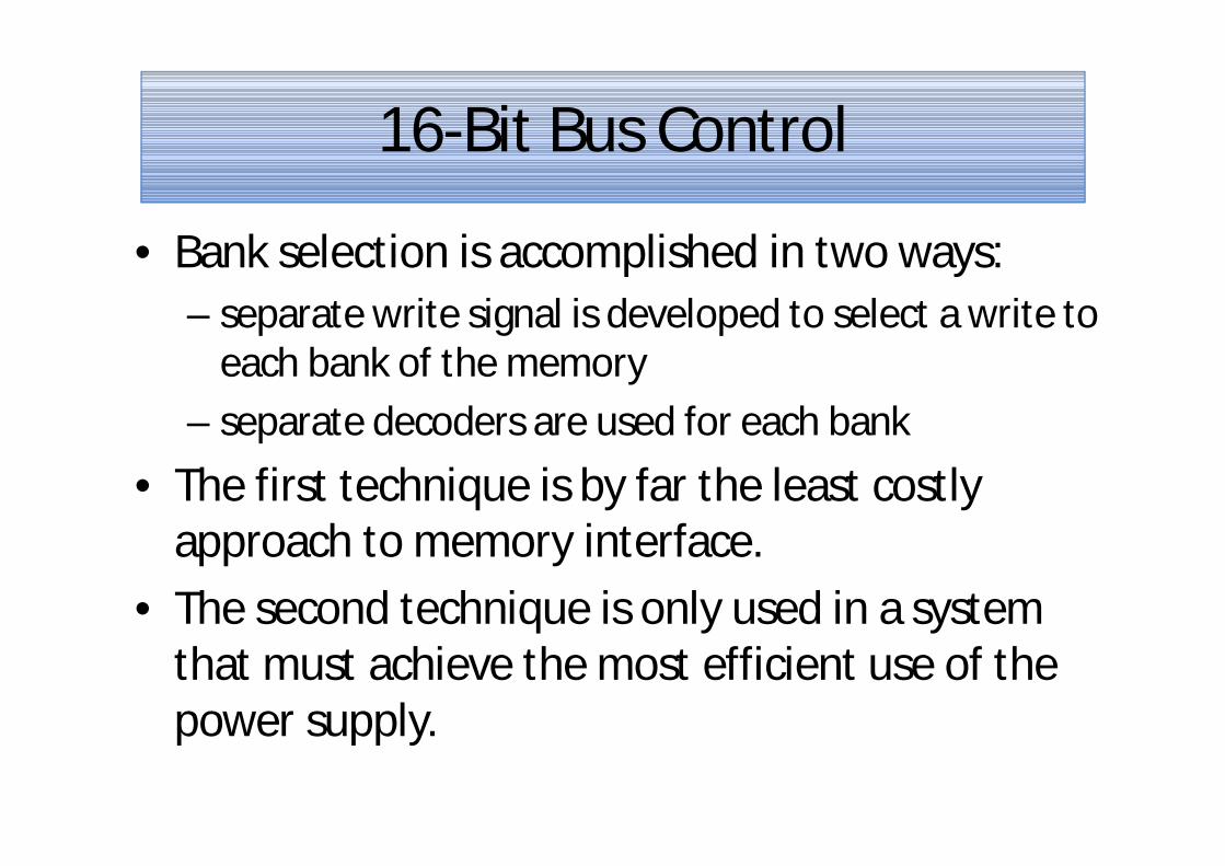
• Bank selection is accomplished in two ways: – separate write signal is developed to select a write to
each bank of the memory – separate decoders are used for each bank
• The first technique is by far the least costly approach to memory interface.
• The second technique is only used in a system that must achieve the most efficient use of the power supply.
16-Bit Bus Control
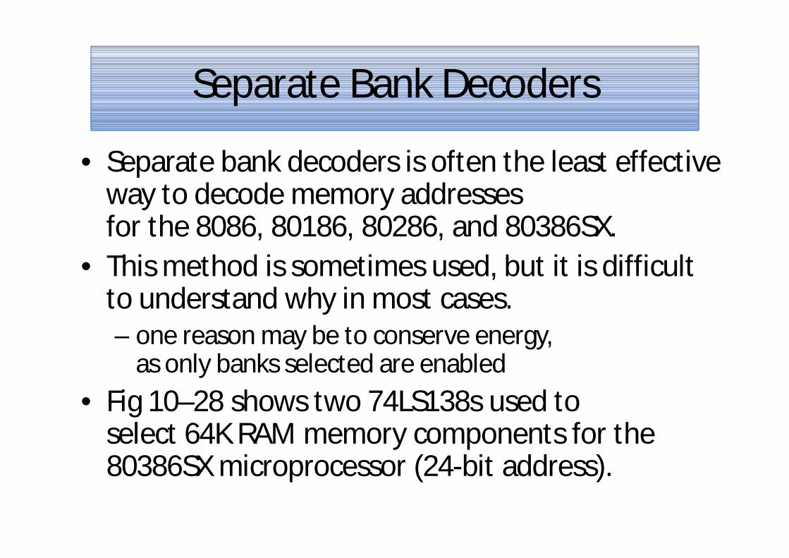
• Separate bank decoders is often the least effective way to decode memory addresses for the 8086, 80186, 80286, and 80386SX.
• This method is sometimes used, but it is difficult to understand why in most cases. – one reason may be to conserve energy,
as only banks selected are enabled • Fig 10–28 shows two 74LS138s used to
select 64K RAM memory components for the 80386SX microprocessor (24-bit address).
Separate Bank Decoders
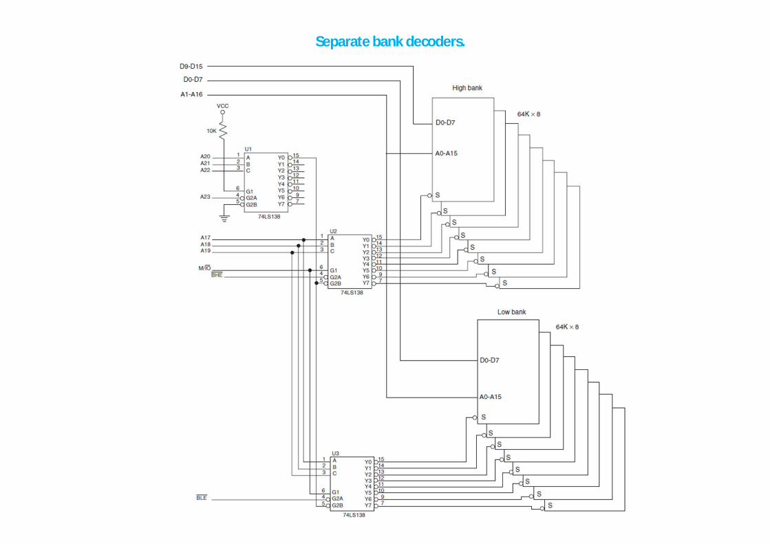
Separate bank decoders.
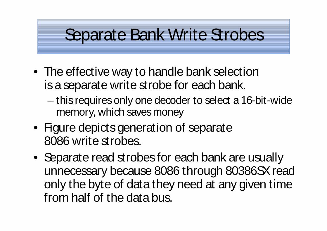
• The effective way to handle bank selection is a separate write strobe for each bank. – this requires only one decoder to select a 16-bit-wide
memory, which saves money • Figure depicts generation of separate
8086 write strobes. • Separate read strobes for each bank are usually
unnecessary because 8086 through 80386SX read only the byte of data they need at any given time from half of the data bus.
Separate Bank Write Strobes
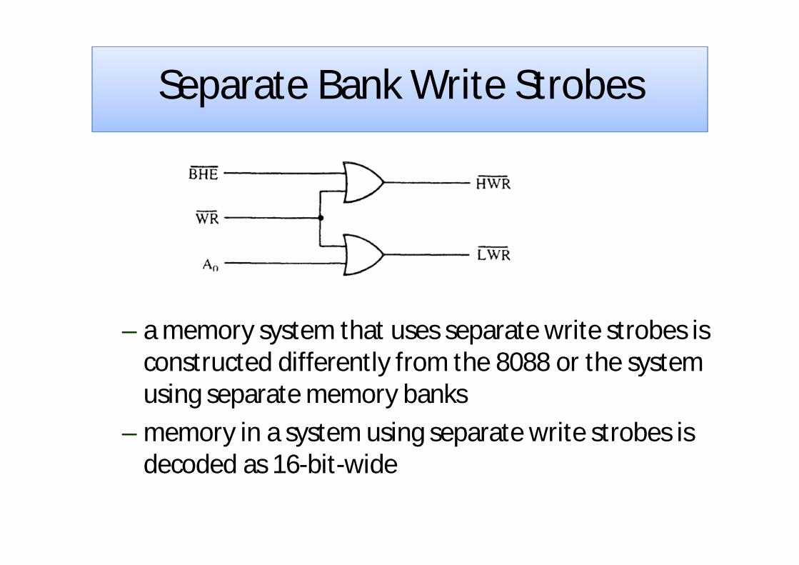
– a memory system that uses separate write strobes is constructed differently from the 8088 or the system using separate memory banks
– memory in a system using separate write strobes is decoded as 16-bit-wide
Separate Bank Write Strobes
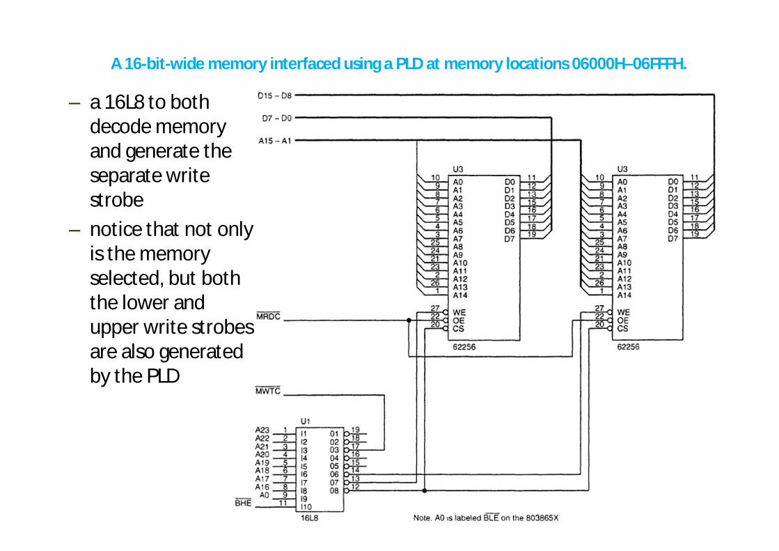
A 16-bit-wide memory interfaced using a PLD at memory locations 06000H–06FFFH.
– a 16L8 to both decode memory and generate the separate write strobe
– notice that not only is the memory selected, but both the lower and upper write strobes are also generated by the PLD
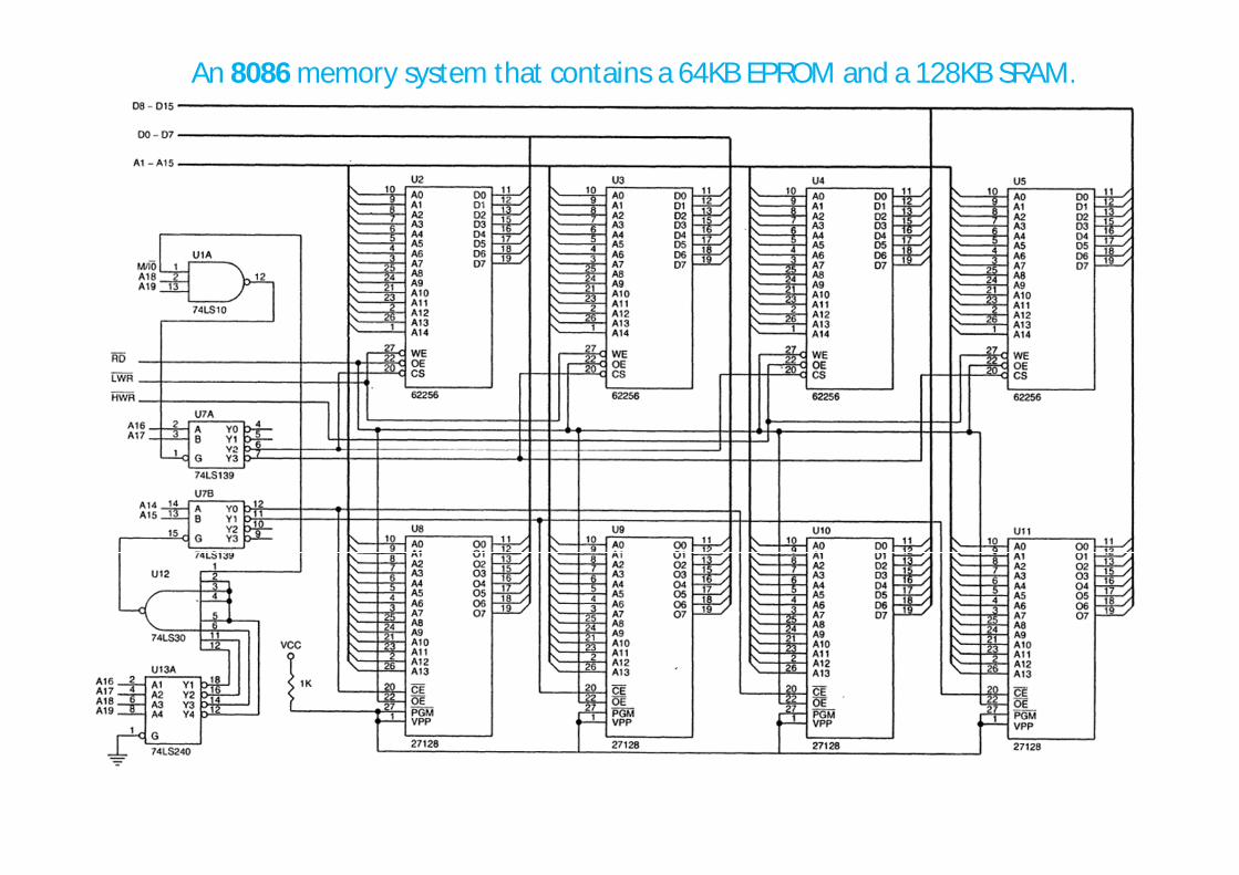
An 8086 memory system that contains a 64KB EPROM and a 128KB SRAM.
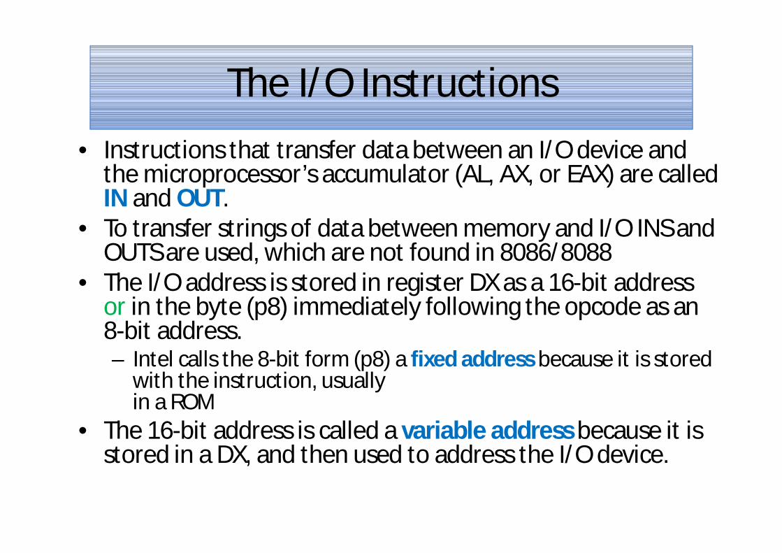
• Instructions that transfer data between an I/O device and the microprocessor’s accumulator (AL, AX, or EAX) are called IN and OUT.
• To transfer strings of data between memory and I/O INS and OUTS are used, which are not found in 8086/8088
• The I/O address is stored in register DX as a 16-bit address or in the byte (p8) immediately following the opcode as an 8-bit address. – Intel calls the 8-bit form (p8) a fixed address because it is stored
with the instruction, usually in a ROM
• The 16-bit address is called a variable address because it is stored in a DX, and then used to address the I/O device.
The I/O Instructions
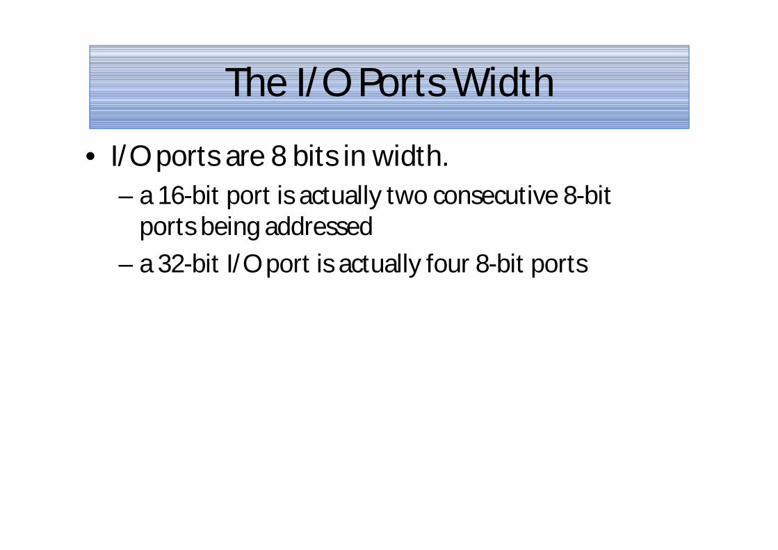
• I/O ports are 8 bits in width.
– a 16-bit port is actually two consecutive 8-bit ports being addressed
– a 32-bit I/O port is actually four 8-bit ports
The I/O Ports Width
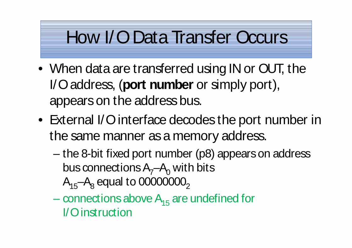
• When data are transferred using IN or OUT, the I/O address, (port number or simply port), appears on the address bus.
• External I/O interface decodes the port number in the same manner as a memory address. – the 8-bit fixed port number (p8) appears on address
bus connections A7–A0 with bits A15–A8 equal to 000000002
– connections above A15 are undefined for I/O instruction
How I/O Data Transfer Occurs
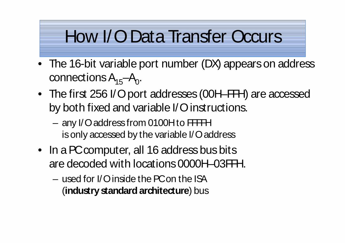
• The 16-bit variable port number (DX) appears on address connections A15–A0.
• The first 256 I/O port addresses (00H–FFH) are accessed by both fixed and variable I/O instructions. – any I/O address from 0100H to FFFFH
is only accessed by the variable I/O address
• In a PC computer, all 16 address bus bits are decoded with locations 0000H–03FFH. – used for I/O inside the PC on the ISA
(industry standard architecture) bus
How I/O Data Transfer Occurs
• Two different methods of interfacing I/O are isolated I/O and memory-mapped I/O.
• In isolated I/O instructions transfer data between the microprocessor’s accumulator or memory and the I/O device.
• In memory-mapped I/O, any instruction that references memory can accomplish the transfer.
• The PC does not use memory-mapped I/O.
Isolated and Memory-Mapped I/O
• The most common I/O transfer technique used in the Intel-based system is isolated I/O.
• In Isolated I/O addresses, called ports, are separate from memory addresses.
• Because the ports are separate, the user can expand the memory to its full size without using any of memory space for I/O devices.
• A disadvantage of isolated I/O is that data transferred between I/O and microprocessor must be accessed by the I/O (IN, OUT) instructions.
• Also, separate control signals for the I/O space are developed (using M/IO and W/R ), which indicate an I/O read (IORC) or an I/O write (RD) operation.
Isolated I/O
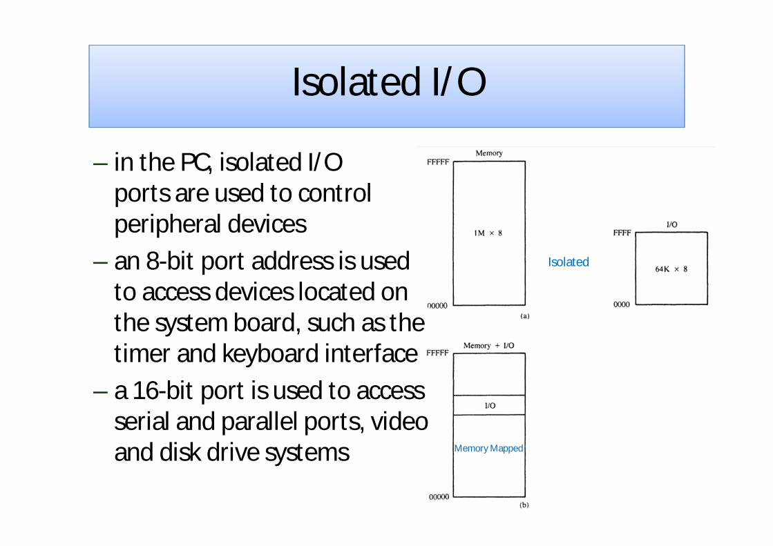
– in the PC, isolated I/O ports are used to control peripheral devices
– an 8-bit port address is used to access devices located on the system board, such as the timer and keyboard interface
– a 16-bit port is used to access serial and parallel ports, video and disk drive systems
Isolated I/O
Memory Mapped
Isolated
• Memory-mapped I/O does not use the I/O instructions. • It treats I/O port as a memory location and uses any
instruction that transfers data between the microprocessor and memory.
• Advantage is any memory transfer instruction can access the I/O device.
• Disadvantage is a portion of memory system is used as the I/O map, reducing available memory
• Some other processors do not have dedicated I/O instructions and therefore use only memory-mapped I/O addressing, e.g. the PowerPC microprocessor (Macintosh computers)
Memory-Mapped I/O
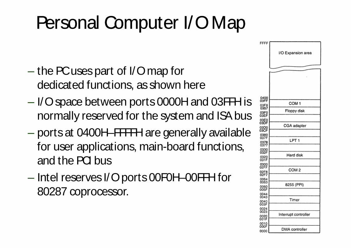
– the PC uses part of I/O map for dedicated functions, as shown here
– I/O space between ports 0000H and 03FFH is normally reserved for the system and ISA bus
– ports at 0400H–FFFFH are generally available for user applications, main-board functions, and the PCI bus
– Intel reserves I/O ports 00F0H–00FFH for 80287 coprocessor.
Personal Computer I/O Map Personal Computer I/O Map
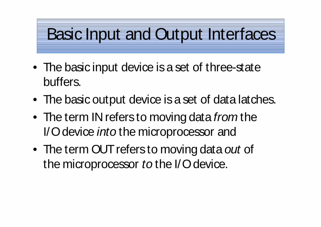
• The basic input device is a set of three-state buffers.
• The basic output device is a set of data latches. • The term IN refers to moving data from the
I/O device into the microprocessor and • The term OUT refers to moving data out of
the microprocessor to the I/O device.
Basic Input and Output Interfaces
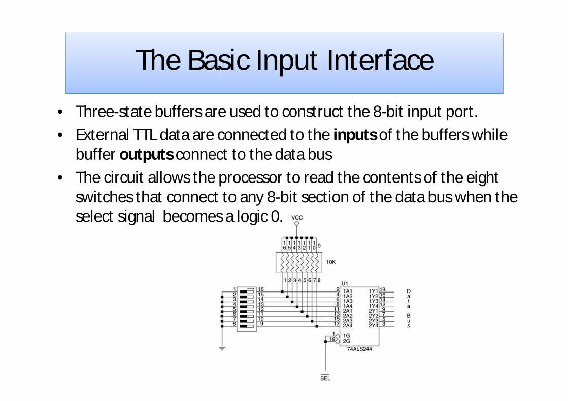
• Three-state buffers are used to construct the 8-bit input port. • External TTL data are connected to the inputs of the buffers while
buffer outputs connect to the data bus • The circuit allows the processor to read the contents of the eight
switches that connect to any 8-bit section of the data bus when the select signal becomes a logic 0.
The Basic Input Interface
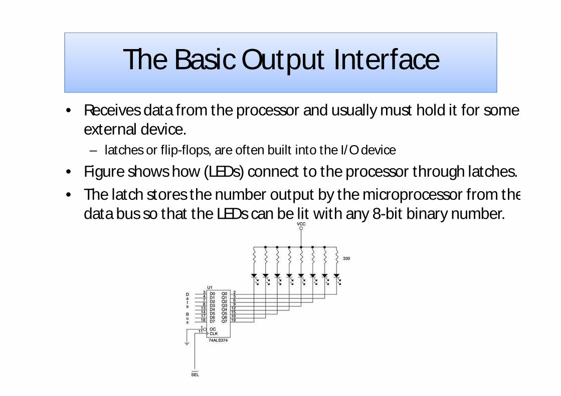
• Receives data from the processor and usually must hold it for some external device. – latches or flip-flops, are often built into the I/O device
• Figure shows how (LEDs) connect to the processor through latches. • The latch stores the number output by the microprocessor from the
data bus so that the LEDs can be lit with any 8-bit binary number.
The Basic Output Interface
• Latches hold the data because when the processor executes an OUT, data are only present on the data bus for less than 1.0 µs. – the viewer would never see the LEDs illuminate
• Each time the OUT executes, the SEL signal activates, capturing data to the latch. – data are held until the next OUT
• When the output instruction is executed, data from the AL register appear on the LEDs.
The Basic Output Interface
• Many I/O devices accept or release information slower than the microprocessor.
• A method of I/O control called handshaking or polling, synchronizes the I/O device with the microprocessor.
• An example is a parallel printer that prints a few hundred characters per second (CPS).
• ASCII data is given to printer, as the printer receives data, it places logic 1 on the BUSY pin, indicating it is printing data
• The software polls or tests the BUSY pin to decide whether the printer is busy. When the BUSY goes low, it sends the second character.
• This process of interrogating the device is called handshaking.
Handshaking
• Very similar to memory address decoding, especially for memory-mapped I/O devices.
• The difference between memory decoding and isolated I/O decoding is the number of address pins connected to the decoder.
• In the personal computer (PC) system, we always decode all 16 bits of the I/O port address.
I/O PORT ADDRESS DECODING
• Fixed I/O instruction uses an 8-bit I/O port address that on A15–A0 as 0000H–00FFH. – we often decode only address connections
A7–A0 for an 8-bit I/O port address – the PC never uses or decodes an 8-bit address
• Figure shows a 74ALS138 decoder that decodes 8-bit I/O ports F0H - F7H. – identical to a memory address decoder except
we only connect address bits A7–A0 to the inputs of the decoder
• The PLD is a better decoder circuit because the number of integrated circuits has been reduced to one device.
Decoding 8-Bit I/O Port Addresses
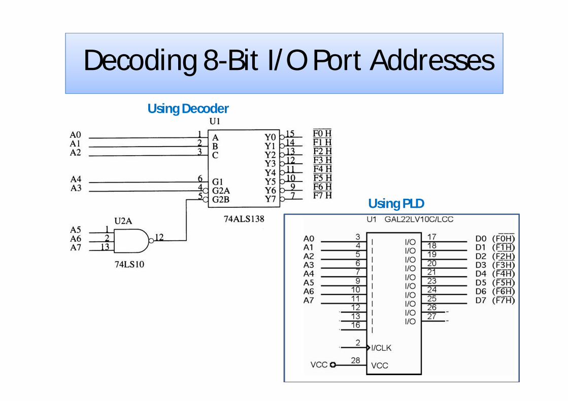
Decoding 8-Bit I/O Port Addresses Using Decoder
Using PLD