Embed Size (px)
Citation preview
Materials Letters 89 (2012) 163–165
Contents lists available at SciVerse ScienceDirect
Materials Letters
0167-57
http://d
n Corr
State Un
fax: þ1
E-m
journal homepage: www.elsevier.com/locate/matlet
Microwave assisted low temperature encapsulation of Ag films by Cureactions using Ag–Cu alloy structures
Sayantan Das a, T.L. Alford a,b,n
a Department of Chemistry and Biochemistry, Arizona State University, Tempe, AZ 85287, United Statesb School for Engineering of Matter, Transport and Energy, Arizona State University, Tempe, AZ 85287, United States
a r t i c l e i n f o
Article history:
Received 27 July 2012
Accepted 14 August 2012Available online 27 August 2012
Keywords:
Thin films
Electrical properties
Segregation
Oxidation
7X/$ - see front matter & 2012 Elsevier B.V.
x.doi.org/10.1016/j.matlet.2012.08.075
esponding author at: Department of Chemist
iversity, Tempe, AZ 85287, United States. Te
480 965 8976.
ail address: [email protected] (T.L. Alford).
a b s t r a c t
Copper (I) oxide (Cu2O) forms an encapsulation layer after annealing Ag–17 at% Cu alloy thin films
inside a microwave cavity. The maximum temperature reached during this process is 70 1C which
makes microwaves an efficient low temperature processing tool for flexible electronics. Rutherford
backscattering spectrometry is used to study the encapsulation of Ag films by copper oxide. X-ray
diffraction shows preferential orientation along the [111] direction for both Ag and Cu2O. Four point
probe measurements suggest that the resistivity is controlled by the residual Cu present in the
alloy films.
& 2012 Elsevier B.V. All rights reserved.
1. Introduction
The gate and source bus lines in thin film transistors for liquidcrystal displays consist of metals like Ta, Ti, Cr and Mo. However,lower resistivity metals like Ag and its alloys are getting muchinterest which will reduce signal delay [1]. However, silver hasserious drawbacks, such as agglomeration at high temperaturesand tarnishing in sulfur rich environments [2]. To resolve theseissues, researchers have focused on forming an encapsulationlayer to prevent silver agglomeration and corrosion in adverseenvironments. Wang and Alford formed aluminum oxynitridediffusion barriers on silver layers [3]. Later, Zeng et al. used anovel encapsulation process which enhanced Ag electromigrationresistance by forming a layer of TiN(O) on the surface [4]. Theencapsulation layers reduced the corrosion of Ag and ensured thestructural integrity of the metal lines.
The above self-encapsulation processes are formed at hightemperatures that make these unsuitable for flexible polymericsubstrates (e.g., 400-700 degrees Celsius [3,4]) like polyethyl-napthalate. One approach is to use microwave (MW) energywhich induces thin film reactions at low temperatures. Typicallybulk metals are excellent reflectors of microwave energy and thusare not heated by microwaves. However, previous studies haveshowed that thin films of gold continuously absorb microwaveradiation and are heated successfully [5]. This is because themicrowave penetration depths (skin depth) for most metals range
All rights reserved.
ry and Biochemistry, Arizona
l.: þ1 480 965 7471;
only a few nanometers. Literature survey reveals that bulkpenetration depths for copper, silver and gold range from 1.3 to1.6 mm at 2.45 GHz [6]. Microwave heating also offers significantadvantages over conventional heating which include: (a) lowerprocessing temperatures, (b) time and energy savings, and(c) improved electrical properties. In this study we use a conven-tional microwave cavity to process Ag–Cu thin films at lowtemperatures which forms a thin Cu-oxide layer on the surface.
2. Experiments
Thin films of Ag–Cu are deposited on Si wafers with 100 nmthick SiNx by co-sputtering 99.99% pure Ag and Cu targets undervacuum. The processing is done inside a 2.45 GHz microwaveoven for different times. A Rayteck Compact MID pryometer isused to measure the sample’s temperature and this pyrometerhas a range of 200 to 1200 degrees Celsius. The thickness and thecompositions of the as-deposited and the MW processed Ag–Cufilms are determined using the Rutherford backscattering spectro-metry (RBS) and RUMP computer simulations [7].
X-ray photoelectron spectroscopy (XPS) was done to confirmthe formation of Cu2O. Four point probe measurements andglancing angle X-ray diffraction (XRD) were done to determinethe electrical and structural properties of the films, respectively.
3. Results and discussions
Heating inside a microwave oven results in a color change ofthe surface–reflective to a reddish color–and shows the formationof a surface layer. The results of RBS characterization are shown in
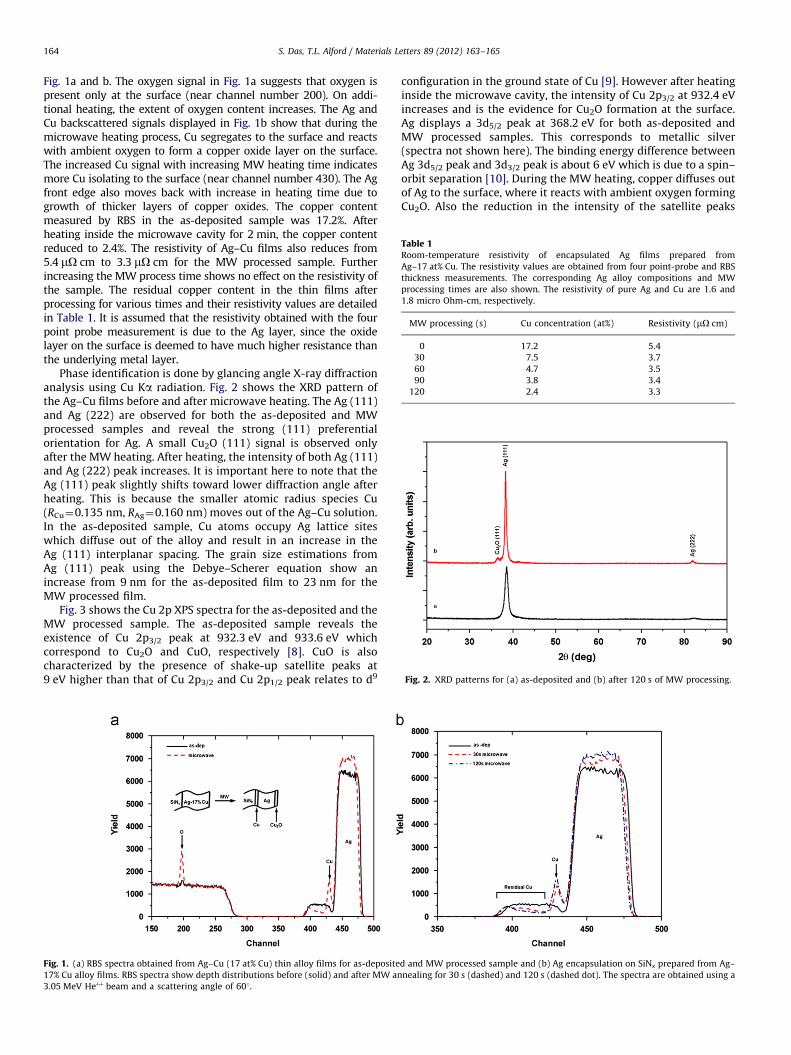
Table 1Room-temperature resistivity of encapsulated Ag films prepared from
Ag–17 at% Cu. The resistivity values are obtained from four point-probe and RBS
thickness measurements. The corresponding Ag alloy compositions and MW
processing times are also shown. The resistivity of pure Ag and Cu are 1.6 and
1.8 micro Ohm-cm, respectively.
MW processing (s) Cu concentration (at%) Resistivity (mO cm)
0 17.2 5.4
30 7.5 3.7
60 4.7 3.5
90 3.8 3.4
120 2.4 3.3
Fig. 2. XRD patterns for (a) as-deposited and (b) after 120 s of MW processing.
S. Das, T.L. Alford / Materials Letters 89 (2012) 163–165164
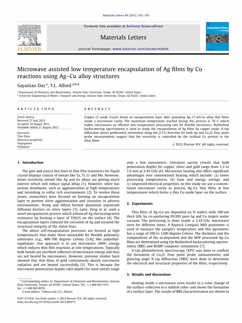
Fig. 1a and b. The oxygen signal in Fig. 1a suggests that oxygen ispresent only at the surface (near channel number 200). On addi-tional heating, the extent of oxygen content increases. The Ag andCu backscattered signals displayed in Fig. 1b show that during themicrowave heating process, Cu segregates to the surface and reactswith ambient oxygen to form a copper oxide layer on the surface.The increased Cu signal with increasing MW heating time indicatesmore Cu isolating to the surface (near channel number 430). The Agfront edge also moves back with increase in heating time due togrowth of thicker layers of copper oxides. The copper contentmeasured by RBS in the as-deposited sample was 17.2%. Afterheating inside the microwave cavity for 2 min, the copper contentreduced to 2.4%. The resistivity of Ag–Cu films also reduces from5.4 mO cm to 3.3 mO cm for the MW processed sample. Furtherincreasing the MW process time shows no effect on the resistivity ofthe sample. The residual copper content in the thin films afterprocessing for various times and their resistivity values are detailedin Table 1. It is assumed that the resistivity obtained with the fourpoint probe measurement is due to the Ag layer, since the oxidelayer on the surface is deemed to have much higher resistance thanthe underlying metal layer.
Phase identification is done by glancing angle X-ray diffractionanalysis using Cu Ka radiation. Fig. 2 shows the XRD pattern ofthe Ag–Cu films before and after microwave heating. The Ag (111)and Ag (222) are observed for both the as-deposited and MWprocessed samples and reveal the strong (111) preferentialorientation for Ag. A small Cu2O (111) signal is observed onlyafter the MW heating. After heating, the intensity of both Ag (111)and Ag (222) peak increases. It is important here to note that theAg (111) peak slightly shifts toward lower diffraction angle afterheating. This is because the smaller atomic radius species Cu(RCu¼0.135 nm, RAg¼0.160 nm) moves out of the Ag–Cu solution.In the as-deposited sample, Cu atoms occupy Ag lattice siteswhich diffuse out of the alloy and result in an increase in theAg (111) interplanar spacing. The grain size estimations fromAg (111) peak using the Debye–Scherer equation show anincrease from 9 nm for the as-deposited film to 23 nm for theMW processed film.
Fig. 3 shows the Cu 2p XPS spectra for the as-deposited and theMW processed sample. The as-deposited sample reveals theexistence of Cu 2p3/2 peak at 932.3 eV and 933.6 eV whichcorrespond to Cu2O and CuO, respectively [8]. CuO is alsocharacterized by the presence of shake-up satellite peaks at9 eV higher than that of Cu 2p3/2 and Cu 2p1/2 peak relates to d9
Fig. 1. (a) RBS spectra obtained from Ag–Cu (17 at% Cu) thin alloy films for as-deposite
17% Cu alloy films. RBS spectra show depth distributions before (solid) and after MW an
3.05 MeV Heþþ beam and a scattering angle of 601.
configuration in the ground state of Cu [9]. However after heatinginside the microwave cavity, the intensity of Cu 2p3/2 at 932.4 eVincreases and is the evidence for Cu2O formation at the surface.Ag displays a 3d5/2 peak at 368.2 eV for both as-deposited andMW processed samples. This corresponds to metallic silver(spectra not shown here). The binding energy difference betweenAg 3d5/2 peak and 3d3/2 peak is about 6 eV which is due to a spin–orbit separation [10]. During the MW heating, copper diffuses outof Ag to the surface, where it reacts with ambient oxygen formingCu2O. Also the reduction in the intensity of the satellite peaks
d and MW processed sample and (b) Ag encapsulation on SiNx prepared from Ag–
nealing for 30 s (dashed) and 120 s (dashed dot). The spectra are obtained using a
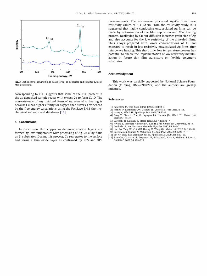
Fig. 3. XPS spectra showing Cu 2p peaks for (a) as-deposited and (b) after 120 s of
MW processing.
S. Das, T.L. Alford / Materials Letters 89 (2012) 163–165 165
corresponding to CuO suggests that some of the CuO present inthe as-deposited sample reacts with excess Cu to form Cu2O. Thenon-existence of any oxidized form of Ag even after heating isbecause Cu has higher affinity for oxygen than silver as evidencedby the free energy calculations using the FactSage 5.4.1 thermo-chemical software and databases [11].
4. Conclusions
In conclusion thin copper oxide encapsulation layers areformed by low temperature MW processing of Ag–Cu alloy filmson Si substrates. During this process, Cu segregates to the surfaceand forms a thin oxide layer as confirmed by RBS and XPS
measurements. The microwave processed Ag–Cu films haveresistivity values of �3 mO cm. From the resistivity study, it issuggested that highly conducting encapsulated Ag films can bemade by optimization of the film deposition and MW heatingprocess. Dealloying by Cu out-diffusion increases grain size of Agand also accounts for the low resistivity of the annealed films.Thus alloys prepared with lower concentrations of Cu areexpected to result in low resistivity encapsulated Ag films aftermicrowave heating. This short time, low temperature process haspotential to enable the implementation of low resistivity metalli-zation in future thin film transistors on flexible polymericsubstrates.
Acknowledgment
This work was partially supported by National Science Foun-dation (C. Ying, DMR-0902277) and the authors are greatlyindebted.
References
[1] Katayama M. Thin Solid Films 1999;341:140–7.[2] Franey JP, Kammlott GW, Graedel TE. Corros Sci 1985;25:133–43.[3] Wang Y, Alford TL. Appl Phys Lett 1999;74:52–4.[4] Zeng Y, Chen L, Zou YL, Nyugen PA, Hansen JD, Alford TL. Mater Lett
2000;45:157–61.[5] Sueyoshi H, Kakiuchi S. Mater Trans 2007;48:531–7.[6] Hwang S, Veronesi P, Leonelli C, Kim H. J Am Ceram Soc 2010;93:3201–5.[7] Doolittle LR. Nucl Instrum Methods Phys Res 1985;B9:344–51.[8] Hou JW, Yang XC, Cui MM, Huang M, Wang QY. Mater Lett 2012;74:159–62.[9] Borgohain K, Murase N, Mahamuni SJ. Appl Phys 2002;92:1292–7.
[10] Lin XF, Zhou RM, Zhang JQ, Fei ST. Appl Surf Sci 2009;256:889–93.[11] Bale CW, Chartrand P, Degterov SA, Eriksson G, Hack K, Mahfoud RB, et al.
CALPHAD 2002;26:189–228.


![Ethiopian Cu-Au-Ag Portfolio · 2019-09-20 · [Cu-Au-Ag] Tigray-Afar [Cu-Au-Ag] 100%. AIM ALS TSX.V ALTS EXPLORE DISCOVER REPEAT 6 One of the world’s top 10 growth countries for](https://img.pdfslide.net/doc/110x75/5f8ae137c3075d766f021025/ethiopian-cu-au-ag-portfolio-2019-09-20-cu-au-ag-tigray-afar-cu-au-ag-100.jpg)