Embed Size (px)
Citation preview
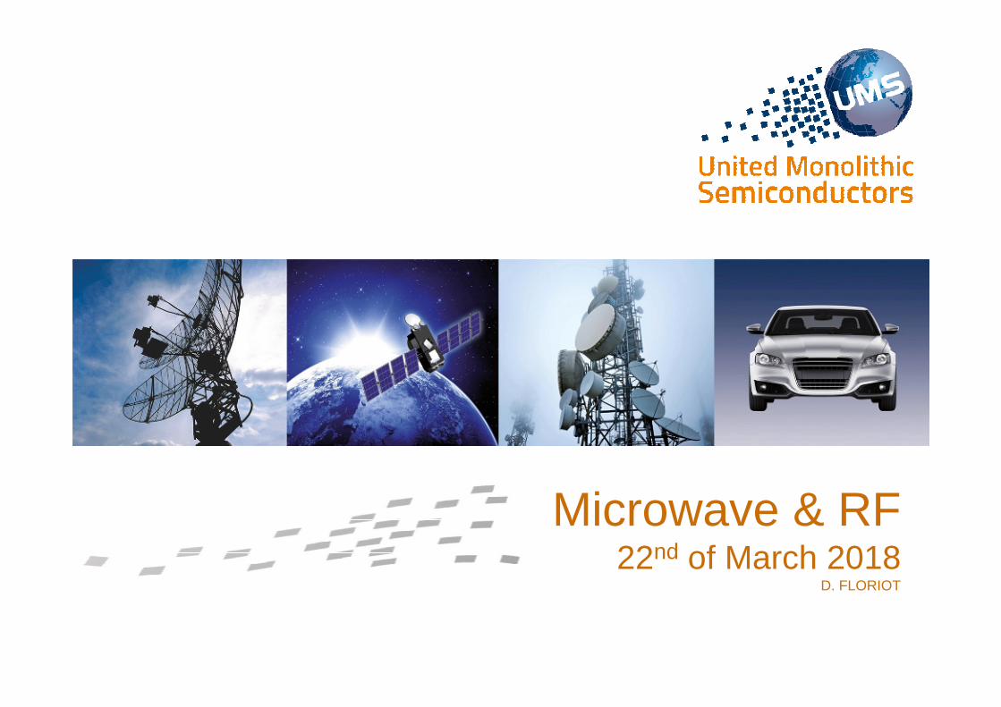
Microwave & RF 22nd of March 2018
D. FLORIOT
� Introduction
� GaN technology roadmap
� GH15-10 : Up to Ka band
Outine
� GH10 : Towards high frequency (Q / V bands)
� GaN : Technology & Integration
2
UMS at a glance
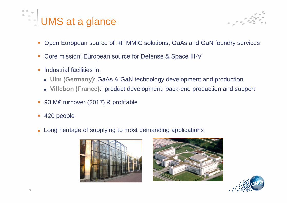
� Open European source of RF MMIC solutions, GaAs and GaN foundry services
� Core mission: European source for Defense & Space III-V
� Industrial facilities in:
� Ulm (Germany): GaAs & GaN technology development and production
� Villebon (France): product development, back-end production and support
� 93 M€ turnover (2017) & profitable� 93 M€ turnover (2017) & profitable
� 420 people
� Long heritage of supplying to most demanding applications
3
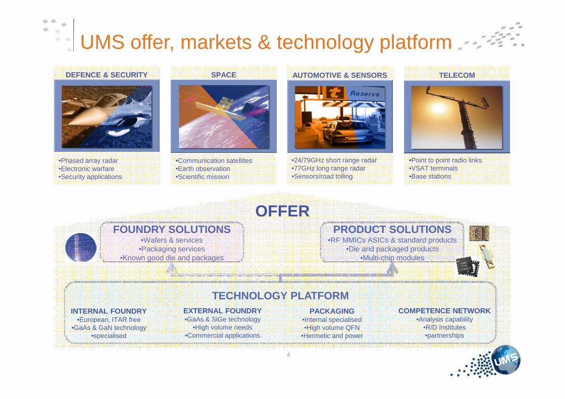
UMS offer, markets & technology platform DEFENCE & SECURITY
•Phased array radar•Electronic warfare•Security applications
SPACE
•Communication satellites•Earth observation•Scientific mission
AUTOMOTIVE & SENSORS
•24/79GHz short range radar•77GHz long range radar•Sensors/road tolling
TELECOM
URE
URE
•Point to point radio links•VSAT terminals•Base stations
4
OFFERFOUNDRY SOLUTIONS
•Wafers & services•Packaging services
•Known good die and packages
PRODUCT SOLUTIONS•RF MMICs ASICs & standard products
•Die and packaged products•Multi-chip modules
TECHNOLOGY PLATFORMINTERNAL FOUNDRY
•European, ITAR free•GaAs & GaN technology
•specialised
EXTERNAL FOUNDRY•GaAs & SiGe technology
•High volume needs•Commercial applications
PACKAGING•Internal specialised•High volume QFN
•Hermetic and power
COMPETENCE NETWORK•Analysis capability
•R/D Institutes•partnerships
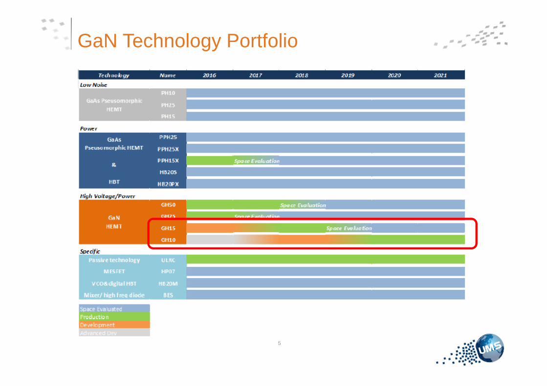
GaN Technology Portfolio
5
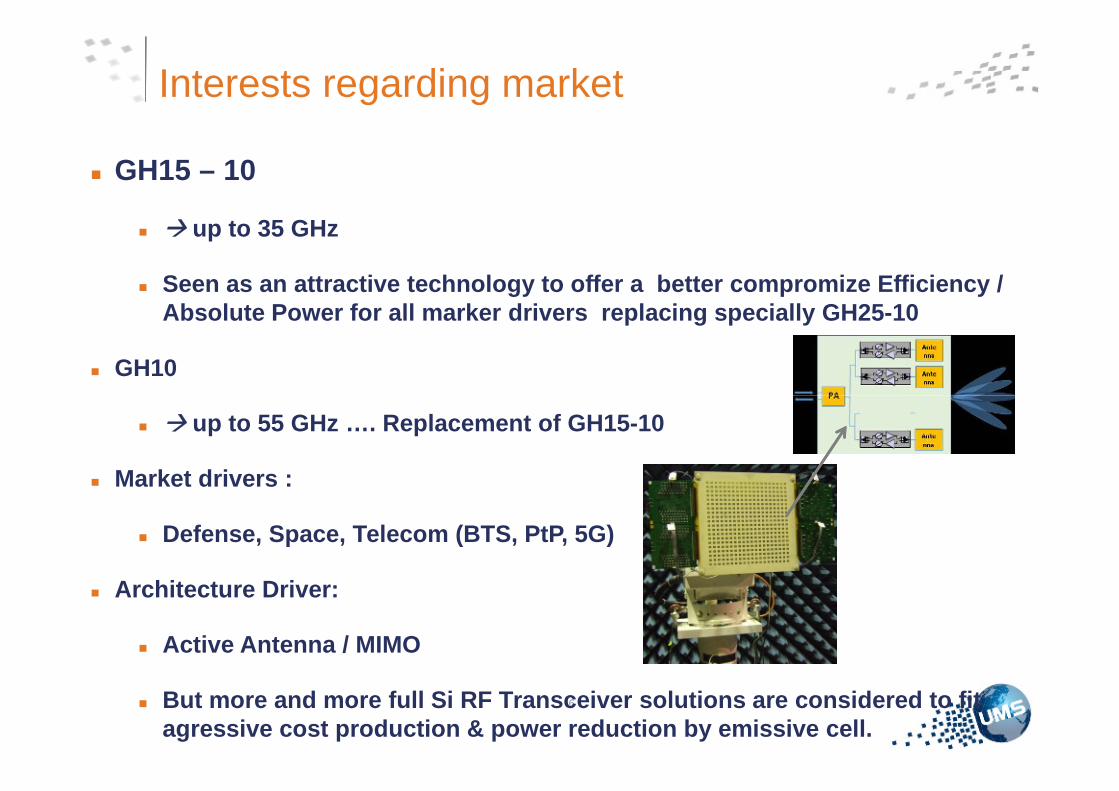
Interests regarding market
� GH15 – 10
� � up to 35 GHz
� Seen as an attractive technology to offer a better com promize Efficiency / Absolute Power for all marker drivers replacing spec ially GH25-10
� GH10
6
� � up to 55 GHz …. Replacement of GH15-10
� Market drivers :
� Defense, Space, Telecom (BTS, PtP, 5G)
� Architecture Driver:
� Active Antenna / MIMO
� But more and more full Si RF Transceiver solutions a re considered to fit agressive cost production & power reduction by emissi ve cell.
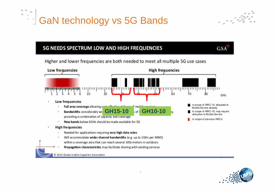
GaN technology vs 5G Bands
7
GH15-10 GH10-10
GH15 Technology
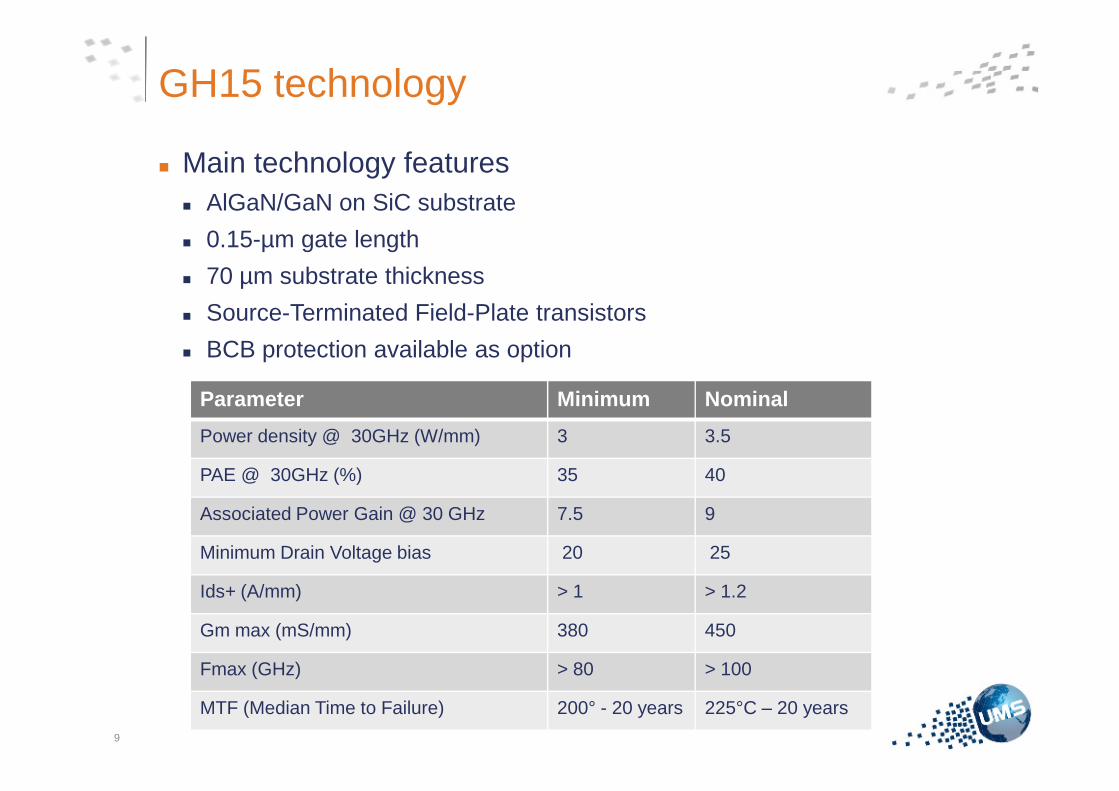
� Main technology features � AlGaN/GaN on SiC substrate
� 0.15-µm gate length
� 70 µm substrate thickness
� Source-Terminated Field-Plate transistors
� BCB protection available as option
GH15 technology
Parameter Minimum Nominal
9
Parameter Minimum Nominal
Power density @ 30GHz (W/mm) 3 3.5
PAE @ 30GHz (%) 35 40
Associated Power Gain @ 30 GHz 7.5 9
Minimum Drain Voltage bias 20 25
Ids+ (A/mm) > 1 > 1.2
Gm max (mS/mm) 380 450
Fmax (GHz) > 80 > 100
MTF (Median Time to Failure) 200° - 20 years 225°C – 20 years
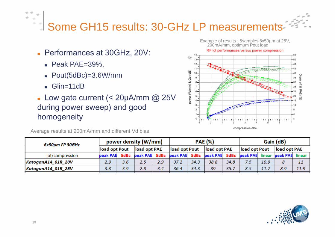
Some GH15 results: 30-GHz LP measurements
� Performances at 30GHz, 20V:� Peak PAE=39%,
� Pout(5dBc)=3.6W/mm
� Glin=11dB
� Low gate current (< 20µA/mm @ 25V during power sweep) and good homogeneity
Example of results : 5samples 6x50µm at 25V, 200mA/mm, optimum Pout load
10
homogeneityAverage results at 200mA/mm and different Vd bias
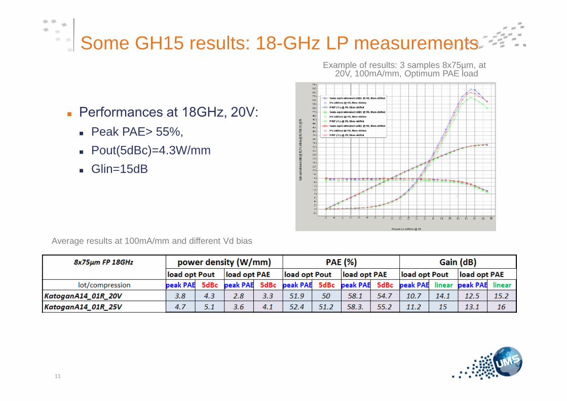
Some GH15 results: 18-GHz LP measurements
� Performances at 18GHz, 20V:� Peak PAE> 55%,
� Pout(5dBc)=4.3W/mm
� Glin=15dB
Example of results: 3 samples 8x75µm, at 20V, 100mA/mm, Optimum PAE load
11
Average results at 100mA/mm and different Vd bias
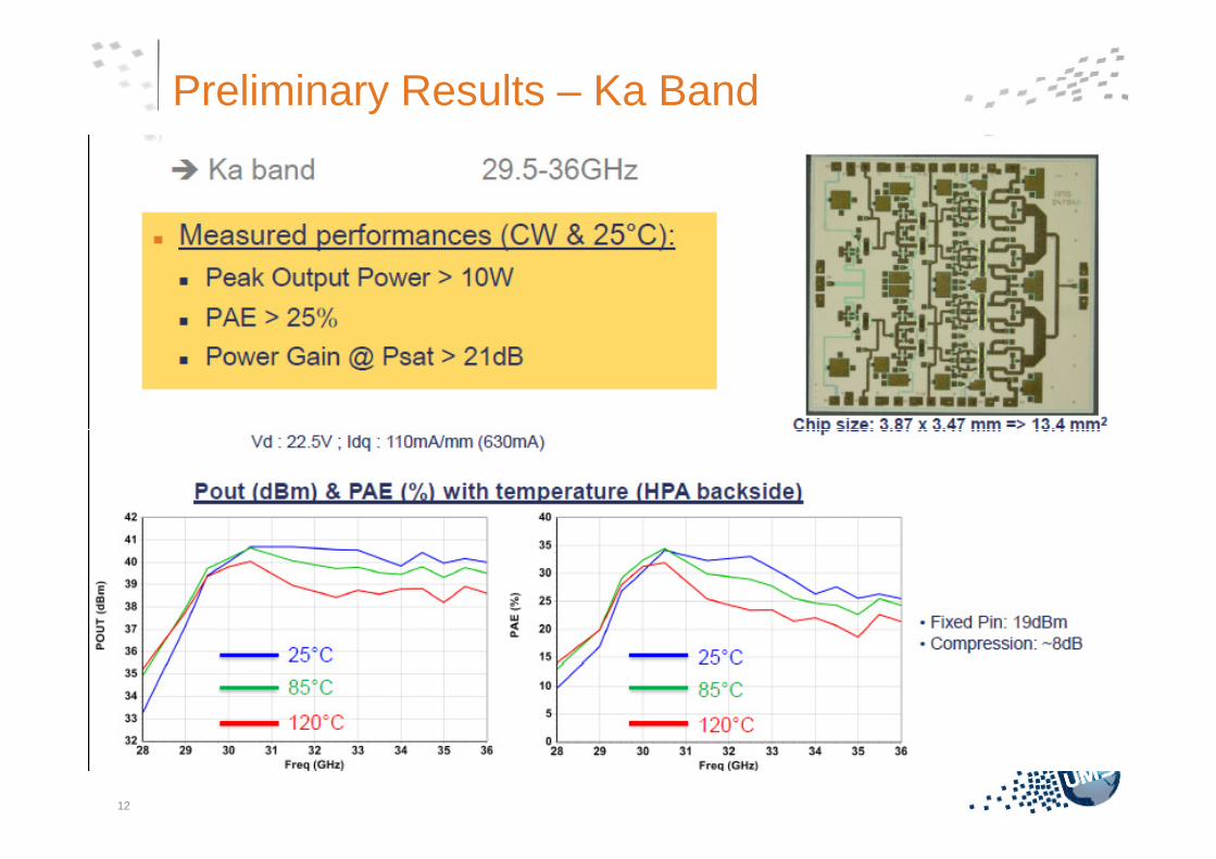
Preliminary Results – Ka Band
12
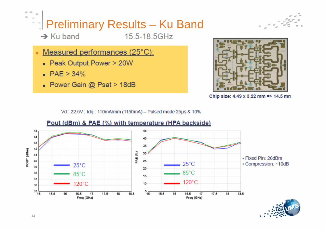
Preliminary Results – Ku Band
13
� Early access in Q2 / 2018
� End of Qualification : Q3 / 2019� Including test to enter into the EPPL / ESA
GH15- 10 - Summary
� Including test to enter into the EPPL / ESA
14

GH10 Technology
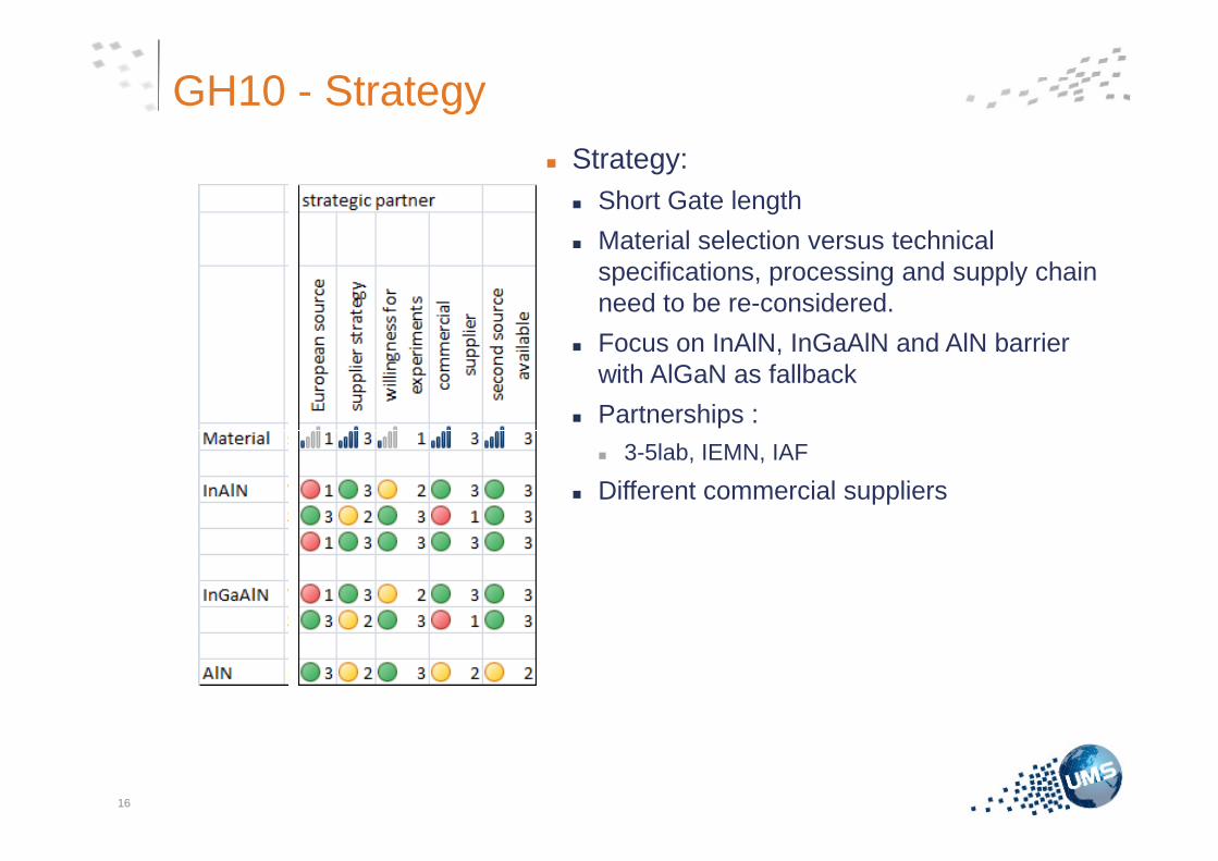
� Strategy:� Short Gate length
� Material selection versus technical specifications, processing and supply chain need to be re-considered.
� Focus on InAlN, InGaAlN and AlN barrier with AlGaN as fallback
� Partnerships :
GH10 - Strategy
� 3-5lab, IEMN, IAF
� Different commercial suppliers
16
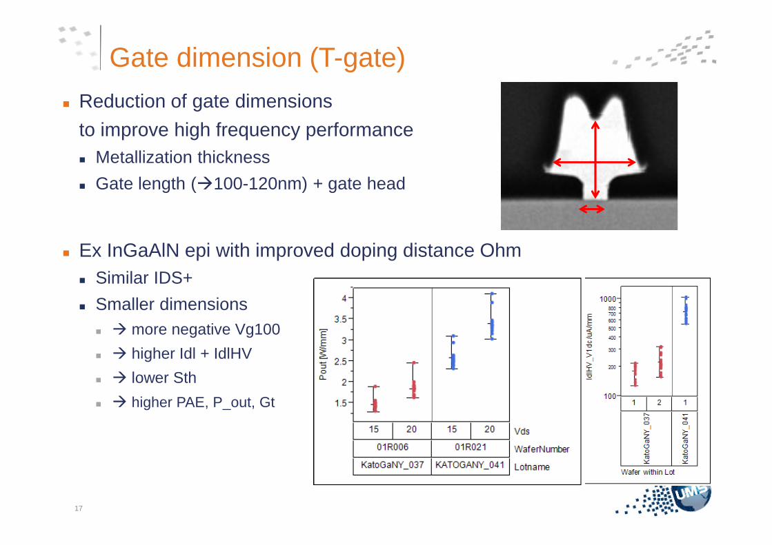
� Reduction of gate dimensions
to improve high frequency performance� Metallization thickness
� Gate length (�100-120nm) + gate head
� Ex InGaAlN epi with improved doping distance OhmSimilar IDS+
Gate dimension (T-gate)
� Similar IDS+
� Smaller dimensions� � more negative Vg100
� � higher Idl + IdlHV
� � lower Sth
� � higher PAE, P_out, Gt
17
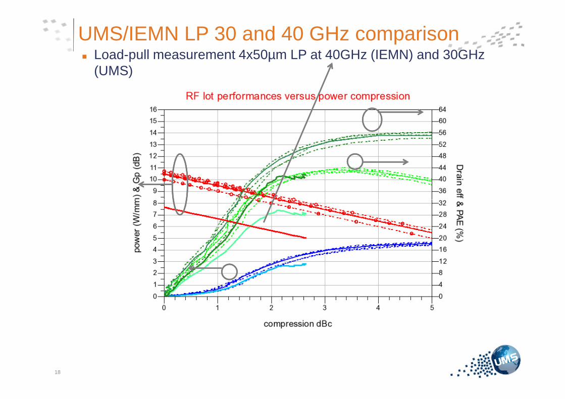
UMS/IEMN LP 30 and 40 GHz comparison� Load-pull measurement 4x50µm LP at 40GHz (IEMN) and 30GHz
(UMS)
18
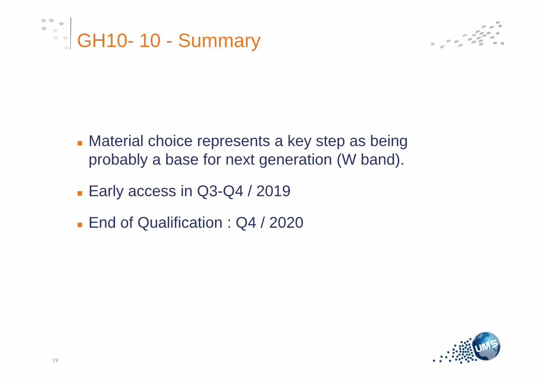
� Material choice represents a key step as being probably a base for next generation (W band).
� Early access in Q3-Q4 / 2019
GH10- 10 - Summary
� Early access in Q3-Q4 / 2019
� End of Qualification : Q4 / 2020
19
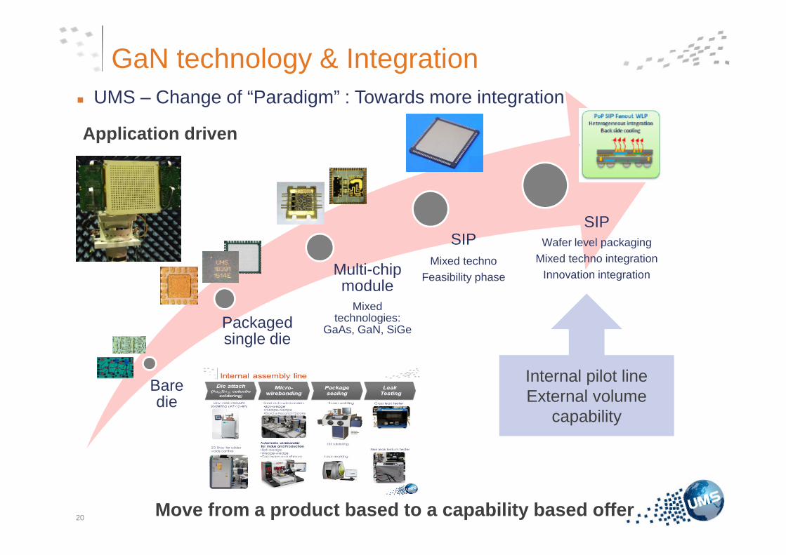
GaN technology & Integration
Multi-chip module
SIPMixed techno
Feasibility phase
SIPWafer level packaging
Mixed techno integrationInnovation integration
Application driven
� UMS – Change of “Paradigm” : Towards more integration
20
Bare die
Packaged single die
Multi-chip module
Mixed technologies:
GaAs, GaN, SiGe
Feasibility phase Innovation integration
Internal pilot lineExternal volume
capability
Move from a product based to a capability based off er
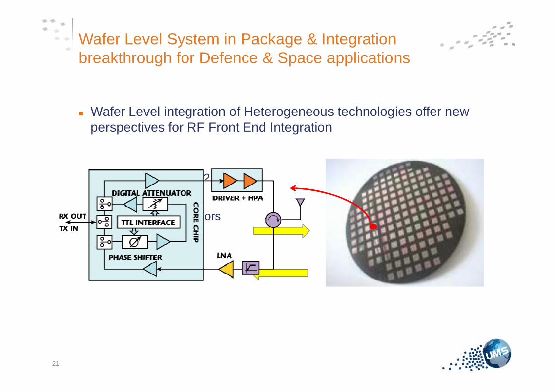
� Wafer Level integration of Heterogeneous technologies offer new perspectives for RF Front End Integration
Wafer Level System in Package & Integration breakthrough for Defence & Space applications
5G_GaN2
21
Demonstrators
� For UMS : to be the key supplier in integrated system of heterogeneous technologies� Cost Benefit due to collective approach at wafer level
� Down scaling in RF electronics at wafer level
� Concept of “One chip - One Front End Module”
Secured and long term access
GaN technology : A breakdown in integration scheme
� Secured and long term access
� Benefit for system platforms� Aerospace
� New generation of Radio / Telecom
� Missile
� Space & Satellite constellation
� Security systems (crypto communicaition)
22
� Route towards System In Package using Wafer Level Packaging approach
� GaN technology with adequate interfaces (bump, hot
GaN technology vs Integration
� GaN technology with adequate interfaces (bump, hot vias, Cu compliant)
� Breakdown in Integration / Cost / Supply chain
23
� Development partly funded by
� THANKS for your attention !
24