Embed Size (px)
Citation preview
Microwave Solid State Devices[Chapter 10]
Prof. Dr. Md. Mostafizur Rahman
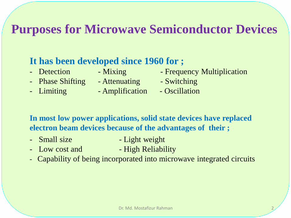
Purposes for Microwave Semiconductor Devices
It has been developed since 1960 for ;- Detection - Mixing - Frequency Multiplication
- Phase Shifting - Attenuating - Switching
- Limiting - Amplification - Oscillation
In most low power applications, solid state devices have replaced
electron beam devices because of the advantages of their ;
- Small size - Light weight
- Low cost and - High Reliability
- Capability of being incorporated into microwave integrated circuits
Dr. Md. Mostafizur Rahman 2

Classification of Microwave Diodes and its Application
Crystal Diodes and Schottky Diodes : For Mixing and Detection
PIN Diode : For Attenuation, Modulation, Switching, Phase shifting and limiting
Varactor Diode : For Frequency Multiplication, Parametric amplification and tuning.
Tunnel Diode and Gun Diode : For Oscillation
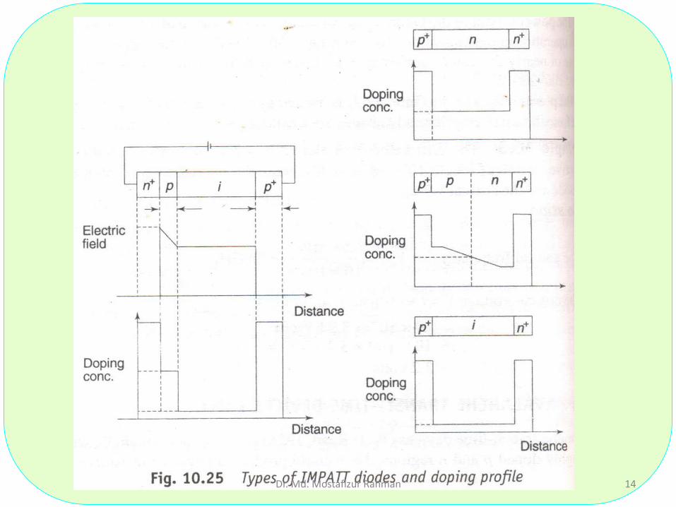
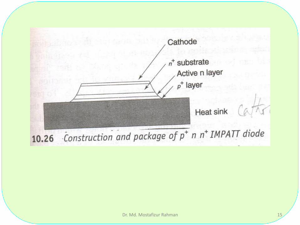
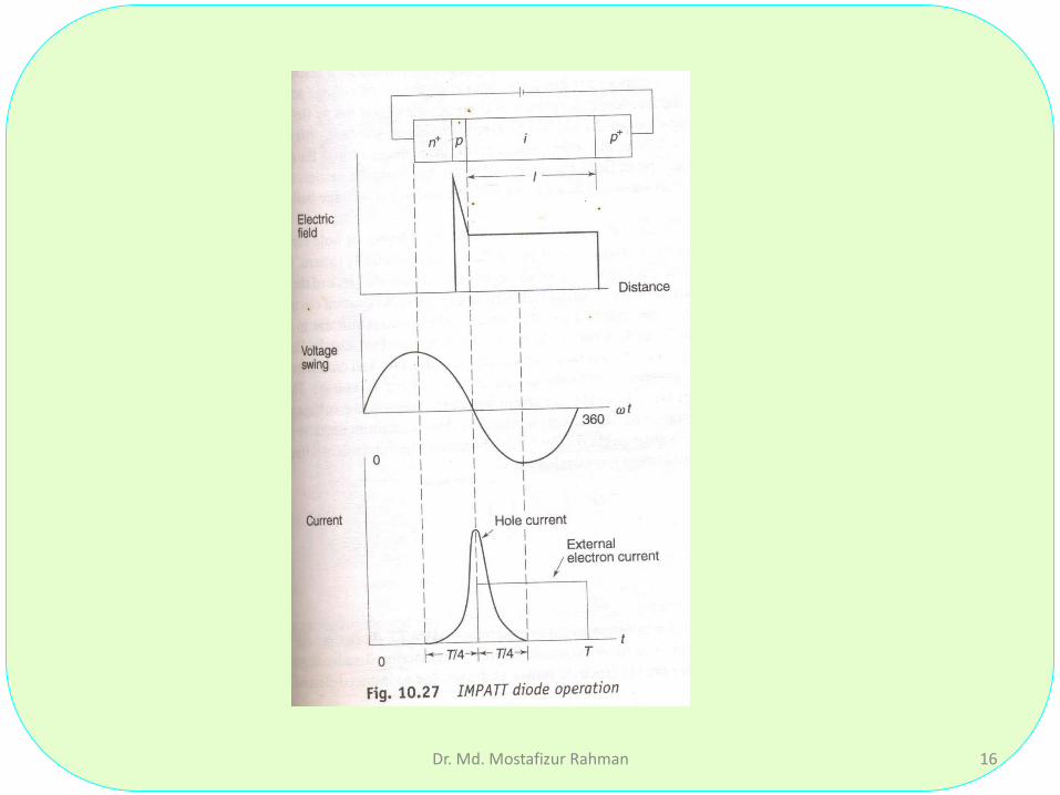
Read Diodes (IMPATT, TRAPATT and BARITT) : For Amplification and Oscillation
IMPATT - Impact Ionization Avalanche Transit Time effect
TRAPATT - Trapped Plasma Avalanche Triggered Transit effect and
BARITT - Barrier Injected Transit Time effect
Dr. Md. Mostafizur Rahman 3

Crystal Diode
Tungsten Wire almost 0.08 mm diameter, P type spring
Wafer almost 1.6 mm square with suitably doped
Ls and Rs is Series Lead Inductance and Resistance
Rj and Cj is the effective Resistance and Capacitance (Rj is small for forward bias and large for reverse bias)
Cc is the case capacitance
Ls and Cc can be tuned out by matching element
Dr. Md. Mostafizur Rahman 4

Schottky Diode
Ls is the inductance of gold whisker wire (0.4 – 0.9 nH)
Rs is bulk resistance of heavy doped Si substrate (4-6 ohm)
Rj is the resistance of metallic Junction
Cj is the barrier Capacitance (0.3 – 0.5 pF)
Cc is the case capacitance
Dr. Md. Mostafizur Rahman 5
Avalanche Transit–Time Devices (ATTD)
Avalanche transit time devices (W T Read, 1958) are p-n junction diode with the highly
doped p and n regions. They could produce a negative resistance at microwave frequencies
by using a carrier impact ionization avalanche breakdown and carriers drift in the high field
intensity region under revers biased condition. There are three types of this devices ;
Impact Ionization Avalanche Transit Time effect (IMPATT)
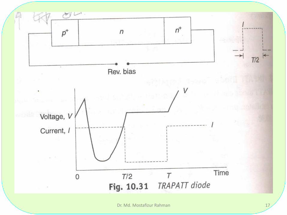
Trapped Plasma Avalanche Triggered Transit (TRAPATT) effect and
Barrier Injected Transit Time (BARITT) effect.
The IMPATT diodes have an efficiency of the order of 3% CW power and 60 % pulsed
power and can be operated from 500 MHz to 100 GHz. The power outputs lie between 1W
(CW) and over 400 W (pulsed). TRAPATT is suitable for low frequency (1-3 GHz)
applications with pulsed power output of several hundred watts and efficiency 20-60%.
BARITT has the advantage of low–noise figures (<15) but with low power and smaller
bandwidth.
Dr. Md. Mostafizur Rahman 6
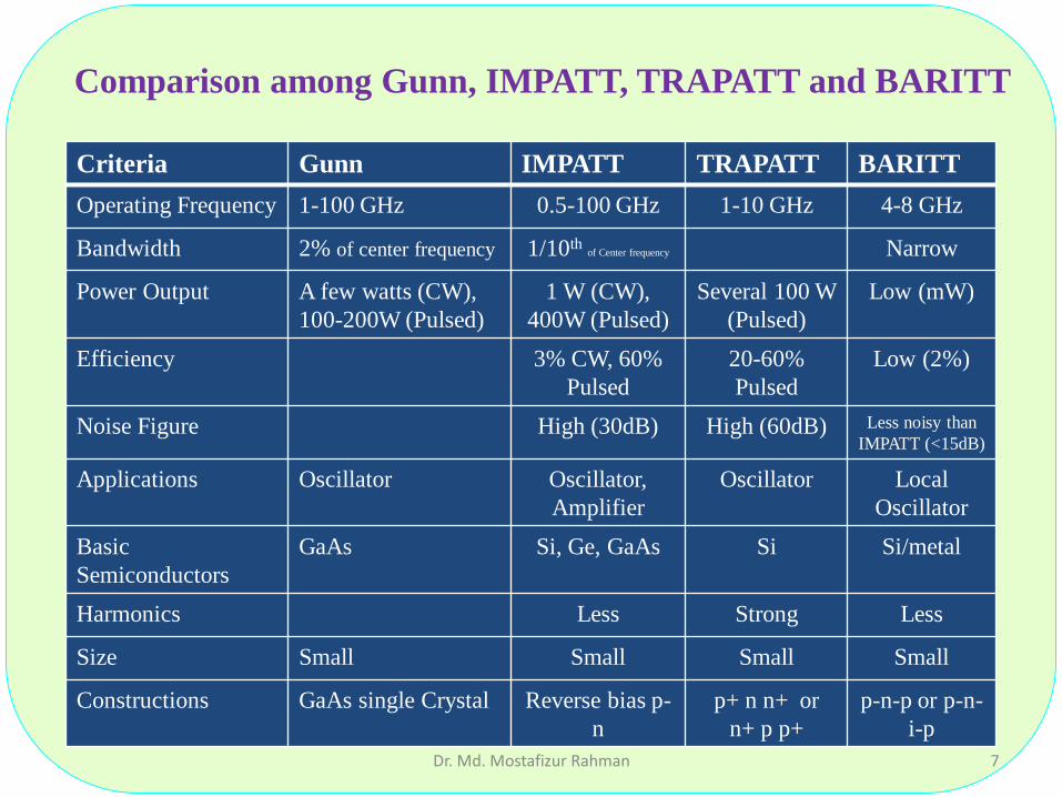
Criteria Gunn IMPATT TRAPATT BARITT
Operating Frequency 1-100 GHz 0.5-100 GHz 1-10 GHz 4-8 GHz
Bandwidth 2% of center frequency 1/10thof Center frequency Narrow
Power Output A few watts (CW),
100-200W (Pulsed)
1 W (CW),
400W (Pulsed)
Several 100 W
(Pulsed)
Low (mW)
Efficiency 3% CW, 60%
Pulsed
20-60%
Pulsed
Low (2%)
Noise Figure High (30dB) High (60dB) Less noisy than
IMPATT (<15dB)
Applications Oscillator Oscillator,
Amplifier
Oscillator Local
Oscillator
Basic
Semiconductors
GaAs Si, Ge, GaAs Si Si/metal
Harmonics Less Strong Less
Size Small Small Small Small
Constructions GaAs single Crystal Reverse bias p-
n
p+ n n+ or
n+ p p+
p-n-p or p-n-
i-p
Comparison among Gunn, IMPATT, TRAPATT and BARITT
Dr. Md. Mostafizur Rahman 7
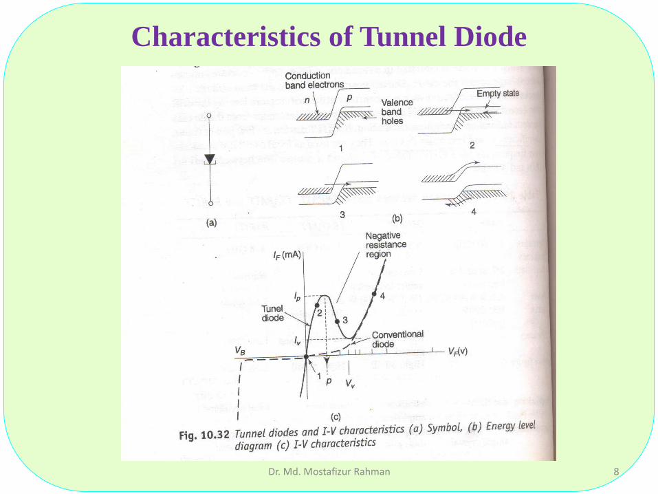
Characteristics of Tunnel Diode
Dr. Md. Mostafizur Rahman 8
Comparison between Tunnel Diode and Normal Diode
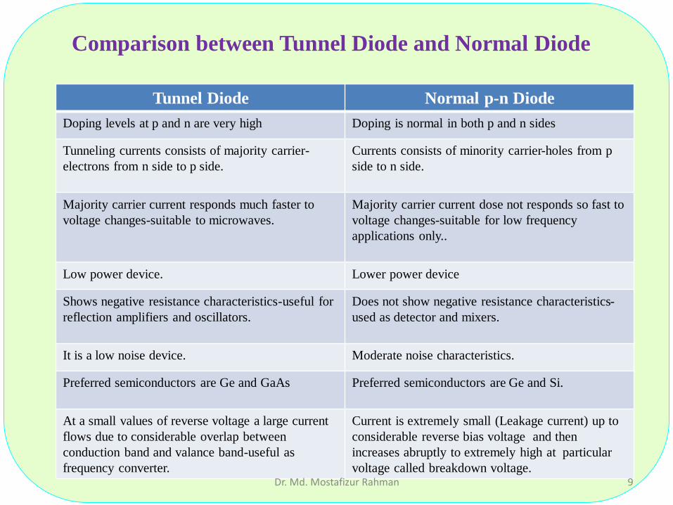
Tunnel Diode Normal p-n Diode
Doping levels at p and n are very high Doping is normal in both p and n sides
Tunneling currents consists of majority carrier-
electrons from n side to p side.
Currents consists of minority carrier-holes from p
side to n side.
Majority carrier current responds much faster to
voltage changes-suitable to microwaves.
Majority carrier current dose not responds so fast to
voltage changes-suitable for low frequency
applications only..
Low power device. Lower power device
Shows negative resistance characteristics-useful for
reflection amplifiers and oscillators.
Does not show negative resistance characteristics-
used as detector and mixers.
It is a low noise device. Moderate noise characteristics.
Preferred semiconductors are Ge and GaAs Preferred semiconductors are Ge and Si.
At a small values of reverse voltage a large current
flows due to considerable overlap between
conduction band and valance band-useful as
frequency converter.
Current is extremely small (Leakage current) up to
considerable reverse bias voltage and then
increases abruptly to extremely high at particular
voltage called breakdown voltage.Dr. Md. Mostafizur Rahman 9

Dr. Md. Mostafizur Rahman 10

Dr. Md. Mostafizur Rahman 11

Dr. Md. Mostafizur Rahman 12
Dr. Md. Mostafizur Rahman 13
Dr. Md. Mostafizur Rahman 14
Dr. Md. Mostafizur Rahman 15
Dr. Md. Mostafizur Rahman 16
Dr. Md. Mostafizur Rahman 17