Embed Size (px)
Citation preview
www.rohm.com 2010.05 - Rev.B© 2010 ROHM Co., Ltd. All rights reserved.
1/17
Middle Power Class-D Speaker Amplifiers
Analog Input / BTL Output Class-D Speaker Amplifier BD5424EFS
Description
BD5424EFS is a 20W + 20W stereo class-D power amplifier IC, developed for space-saving and low heat-generation applications such as low-profile TV sets. The IC employs state-of-the-art Bipolar, CMOS, and DMOS (BCD) process technology that eliminates turn-on resistance in the output power stage and internal loss due to line resistances up to an ultimate level. With this technology, the IC has achieved high efficiency of 91% (10W + 10W output with 8Ω load), which is the top class in the industry. The IC, in addition, employs a compact back-surface heat radiation type power package to achieve low power consumption and low heat generation and eliminates necessity of installing an external radiator, up to a total output of 40W. This product satisfies both needs for drastic downsizing, low-profile structures and powerful, high-quality playback of the sound system.
Features
1) A high efficiency of 91% (10W + 10W output with 8Ω load), which is the highest grade in the industry and low heat-generation. 2) An output of 20W + 20W (17V, with 8Ω load) is allowed without an external heat radiator. 3) Driving a lowest rating load of 3.6Ω is allowed. 4) Pop noise upon turning power on/off and power interruption has been reduced. 5) High-quality audio muting is implemented by soft-switching technology. 6) An output power limiter function limits excessive output to speakers. 7) High-reliability design provided with built-in protection circuits against high temperatures, against VCC shorting and
GND shorting, against reduced-voltage, and against applying DC voltage to speaker. 8) A master/slave function allowing synchronization of multiple devices reduces beat noises. 9) Adjustment of internal PWM sampling clock frequencies (350kHz to 500kHz) allows easy protective measures
against unwanted radio emission to AM radio band. 10) A compact back-surface heat radiation type power package is employed. HTSSOP-A44 (5mm × 7.5mm × 1.0mm, pitch 0.8mm)
Absolute Maximum Ratings
A circuit must be designed and evaluated not to exceed absolute maximum rating in any cases and even momentarily, to prevent reduction in functional performances and thermal destruction of a semiconductor product and secure useful life and reliability.
The following values assume Ta =25. For latest values, refer to delivery specifications.
Parameter Symbol Ratings Unit Conditions
Supply voltage VCC +20 V Pin 7, 8, 15, 16, 29, 30, 37, 38, 40 (Note 1, 2)
Power dissipation Pd 2.0 W (Note 3) 4.5 W (Note 4)
Input voltage for signal pin VIN -0.2 ~ +7.2 V Pin 1, 44 (Note 1)
Input voltage for control pin VCONT -0.2 ~ Vcc+0.2 V Pin 20, 24 (Note 1)
Input voltage for clock pin VOSC -0.2 ~ +7.2 V Pin 23 (Note 1)
Operating temperature range Topr -40 ~ +85
Storage temperature range Tstg -55 ~ +150
Maximum junction temperature Tjmax +150 (Note 1) A voltage that can be applied with reference to GND (pins 11, 12, 33, 34, and 43) (Note 2) Pd and Tjmax=150 must not be exceeded. (Note 3) 70mm × 70mm × 1.6mm FR4 One-sided glass epoxy board (Back copper foil 0%) installed. If used under Ta=25 or higher, reduce 16mW for increase of every 1. The board is provided with thermal via. (Note 4) 70mm × 70mm × 1.6mm FR4 Both-sided glass epoxy board (Back copper foil 100%) installed. If used under Ta=25 or higher, reduce 36mW for increase of every 1. The board is provided with thermal via.
No.10075EBT04
Technical Note
www.rohm.com 2010.05 - Rev.B© 2010 ROHM Co., Ltd. All rights reserved.
2/17
BD5424EFS
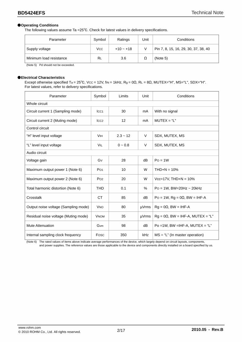
Operating Conditions The following values assume Ta =25. Check for latest values in delivery specifications.
Parameter Symbol Ratings Unit Conditions
Supply voltage VCC +10 ~ +18 V Pin 7, 8, 15, 16, 29, 30, 37, 38, 40
Minimum load resistance RL 3.6 Ω (Note 5) (Note 5) Pd should not be exceeded.
Electrical Characteristics
Except otherwise specified Ta = 25, VCC = 12V, fIN = 1kHz, Rg = 0Ω, RL = 8Ω, MUTEX="H", MS="L", SDX="H". For latest values, refer to delivery specifications.
Parameter Symbol Limits Unit Conditions
Whole circuit
Circuit current 1 (Sampling mode) ICC1 30 mA With no signal
Circuit current 2 (Muting mode) ICC2 12 mA MUTEX = “L”
Control circuit
“H” level input voltage VIH 2.3 ~ 12 V SDX, MUTEX, MS
“L” level input voltage VIL 0 ~ 0.8 V SDX, MUTEX, MS
Audio circuit
Voltage gain GV 28 dB PO = 1W
Maximum output power 1 (Note 6) PO1 10 W THD+N = 10%
Maximum output power 2 (Note 6) PO2 20 W Vcc=17V, THD+N = 10%
Total harmonic distortion (Note 6) THD 0.1 % PO = 1W, BW=20Hz ~ 20kHz
Crosstalk CT 85 dB PO = 1W, Rg = 0Ω, BW = IHF-A
Output noise voltage (Sampling mode) VNO 80 µVrms Rg = 0Ω, BW = IHF-A
Residual noise voltage (Muting mode) VNOM 35 µVrms Rg = 0Ω, BW = IHF-A, MUTEX = “L”
Mute Attenuation Gvm 98 dB Po =1W, BW =IHF-A, MUTEX = “L”
Internal sampling clock frequency FOSC 350 kHz MS = “L” (In master operation) (Note 6) The rated values of items above indicate average performances of the device, which largely depend on circuit layouts, components, and power supplies. The reference values are those applicable to the device and components directly installed on a board specified by us.
Technical Note
www.rohm.com 2010.05 - Rev.B© 2010 ROHM Co., Ltd. All rights reserved.
3/17
BD5424EFS
0.01
0.1
1
10
100
0.001 0.01 0.1 1 10 100
OUTPUT POWER (W)
TH
D+N
(%)
100Hz1kHz
6kHz
Vcc=12V
RL=8Ω
BW=20~20kHz
0.01
0.1
1
10
100
10 100 1000 10000 100000
FREQUENCY (Hz)
TH
D+N
(%)
Vcc=12V
RL=8Ω
Po=1W
BW=20~20kHz
0
5
10
15
20
25
30
35
40
10 100 1000 10000 100000
FREQUENCY (Hz)
VO
LTA
GE G
AIN
(dB
)
Vcc=12V
RL=8Ω
Po=1W
L=33µH
C=0.47µF
Cg=0.1µF
-100
-80
-60
-40
-20
0
10 100 1000 10000 100000
FREQUENCY (Hz)
CR
OSSTA
LK (dB
)Vcc=12V
RL=8Ω
Po=1W
BW=20~20kHz
-100
-80
-60
-40
-20
0
0.001 0.01 0.1 1 10 100
OUTPUT POWER (W)
CR
OSSTA
LK (
dB)
Vcc=12V
RL=8Ω
fin=1kHz
BW=20~20kHz
0
5
10
15
20
25
8 10 12 14 16 18 20
VCC (V)
OU
TP
UT
PO
WER
(W
) THD=10%
THD=1%
RL=8Ω
fin=1kHz
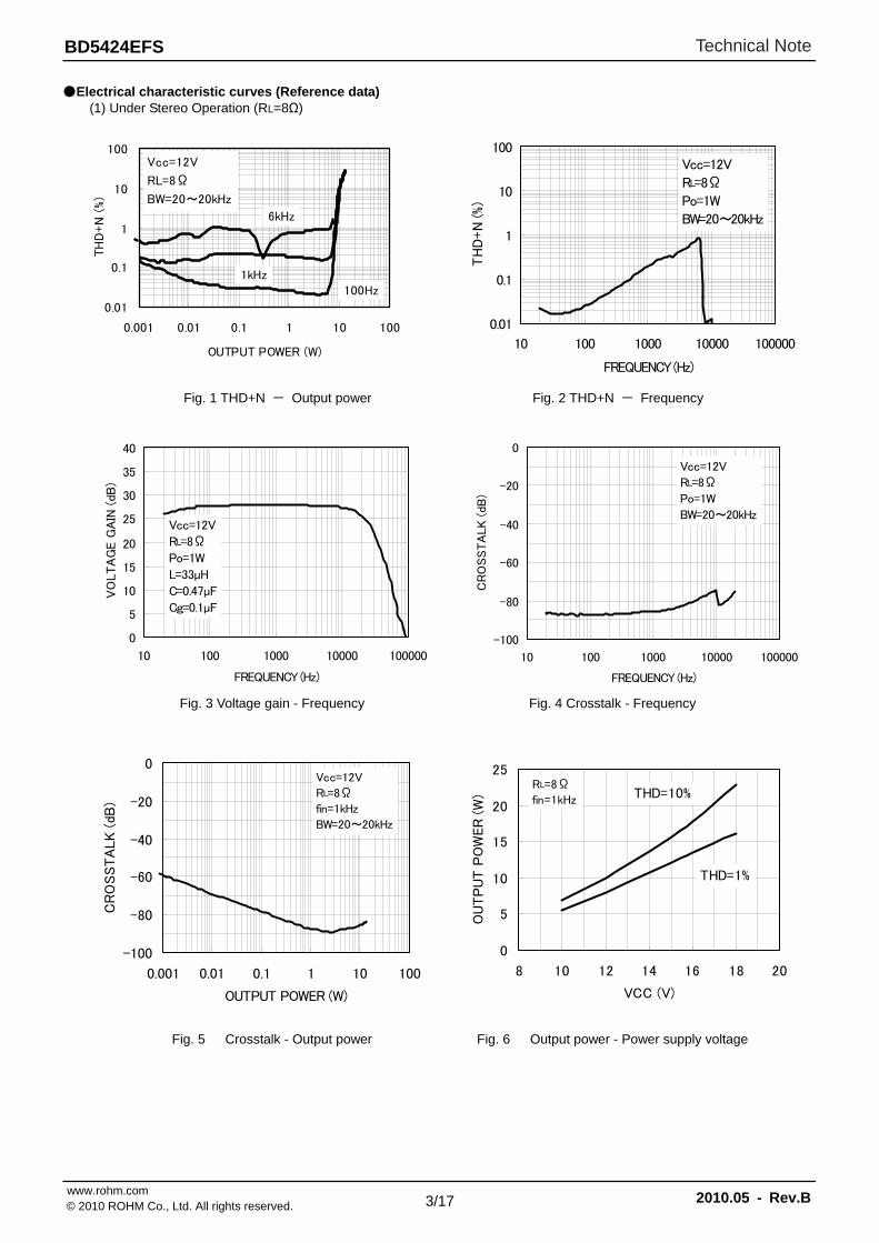
Electrical characteristic curves (Reference data) (1) Under Stereo Operation (RL=8Ω)
Fig. 1 THD+N - Output power Fig. 2 THD+N - Frequency
Fig. 3 Voltage gain - Frequency Fig. 4 Crosstalk - Frequency
Fig. 5 Crosstalk - Output power Fig. 6 Output power - Power supply voltage
Technical Note
www.rohm.com 2010.05 - Rev.B© 2010 ROHM Co., Ltd. All rights reserved.
4/17
BD5424EFS
0
10
20
30
40
50
60
70
80
90
100
0 5 10 15 20
OUTPUT POWER (W/ch)
EFFIC
IEN
CY
(%)
Vcc=12VRL=8Ω
fin=1kHz
0
10
20
30
40
50
60
70
80
90
100
0 5 10 15 20
OUTPUT POWER (W/ch)
EFFIC
IEN
CY
(%)
Vcc=10VRL=8Ω
fin=1kHz
01020304050
60708090
100
0 5 10 15 20 25
OUTPUT POWER (W/ch)
EFFIC
IEN
CY
(%)
Vcc=18V
RL=8Ω
fin=1kHz
0
1
2
3
0 5 10 15 20 25 30 35 40 45 50
TOTAL OUTPUT POWER (W)
ICC
(A
)
Vcc=10V
Vcc=12V
Vcc=18V
RL=8Ω
fin=1kHz
-140
-120
-100
-80
-60
-40
-20
0
10 100 1000 10000 100000
FREQUENCY (Hz)
NO
ISE F
FT (dB
V)
Vcc=12V
RL=8Ω
無信号時
BW=20~20kHz
0
10
2030
40
50
607080
90100
8 10 12 14 16 18
VCC (V)
ICC
(m
A)
Sampling
Mute
RL=8Ω
無信号時
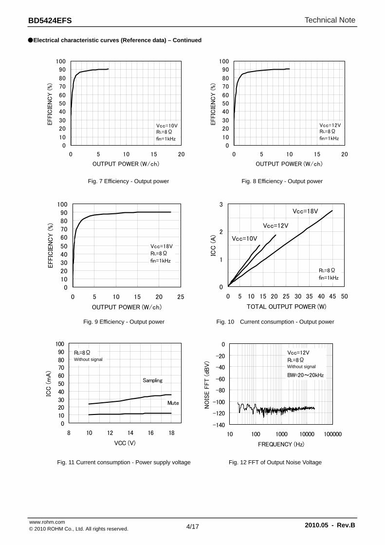
Electrical characteristic curves (Reference data) – Continued
Fig. 7 Efficiency - Output power Fig. 8 Efficiency - Output power
Fig. 9 Efficiency - Output power Fig. 10 Current consumption - Output power
Fig. 11 Current consumption - Power supply voltage Fig. 12 FFT of Output Noise Voltage
Without signal
Without signal
Technical Note
www.rohm.com 2010.05 - Rev.B© 2010 ROHM Co., Ltd. All rights reserved.
5/17
BD5424EFS
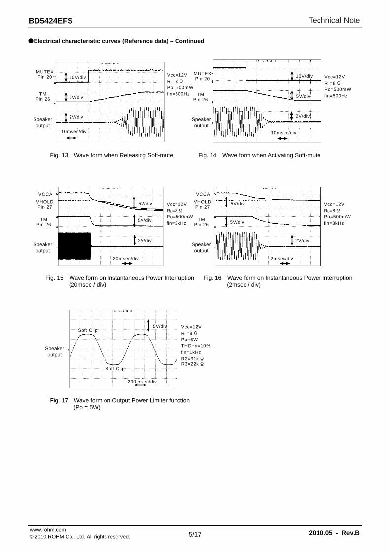
Electrical characteristic curves (Reference data) – Continued
MUTEXPin 20
TMPin 26
10msec/div
2V/div
5V/div
10V/div Vcc=12VRL =8 Ω
Po=500mWfin=500Hz
MUTEXPin 20
TMPin 26
10msec/div
2V/div
5V/div
10V/div Vcc=12VRL=8 Ω
Po=500mWfin=500Hz
Speaker output
Speaker output
Fig. 13 Wave form when Releasing Soft-mute Fig. 14 Wave form when Activating Soft-mute
VCCA
VHOLDPin 27
Vcc=12VRL =8 Ω
Po=500mWfin=3kHz
20msec/div
2V/div
5V/div
5V/divTMPin 26
VCCA
VHOLDPin 27
Vcc=12VRL=8 Ω
Po=500mWfin=3kHz
2msec/div
2V/div
5V/div
5V/divTM
Pin 26
Speaker output
Speaker output
Fig. 15 Wave form on Instantaneous Power Interruption(20msec / div)
Fig. 16 Wave form on Instantaneous Power Interruption (2msec / div)
Vcc=12VRL=8 Ω
Po=5WTHD+n=10%fin=1kHzR2=91k ΩR3=22k Ω
200μsec/div
5V/divSoft Clip
Soft Clip
Speaker output
Fig. 17 Wave form on Output Power Limiter function (Po = 5W)
Technical Note
www.rohm.com 2010.05 - Rev.B© 2010 ROHM Co., Ltd. All rights reserved.
6/17
BD5424EFS
0
5
10
15
20
25
30
8 10 12 14 16 18 20
VCC (V)
OU
TP
UT
PO
WER
(W
) THD=10%RL=6Ω
fin=1kHz
0
10
20
30
40
50
60
70
80
90
100
0 5 10 15 20 25
OUTPUT POWER (W/ch)
EFFIC
IEN
CY (
%)
Vcc=10V
RL=6Ω
fin=1kHz
0
10
20
30
40
50
60
70
80
90
100
0 5 10 15 20 25
OUTPUT POWER (W/ch)
EFFIC
IEN
CY (
%)
Vcc=12V
RL=6Ω
fin=1kHz
0
1020
30
4050
60
70
8090
100
0 5 10 15 20 25 30
OUTPUT POWER (W/ch)
EFFIC
IEN
CY
(%)
Vcc=18V
RL=6Ω
fin=1kHz
0
1
2
3
4
0 5 10 15 20 25 30 35 40 45 50 55 60
TOTAL OUTPUT POWER (W)
ICC
(A
) Vcc=10V
Vcc=12V
Vcc=18V
RL=6Ω
fin=1kHz
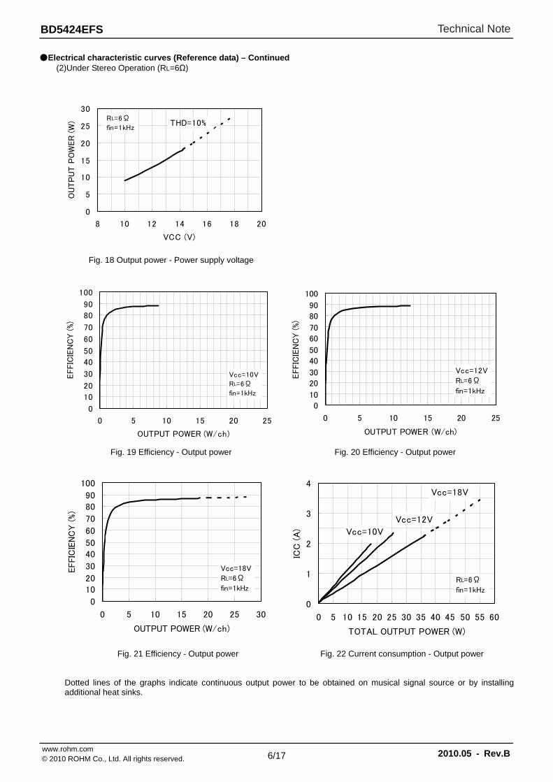
Electrical characteristic curves (Reference data) – Continued (2)Under Stereo Operation (RL=6Ω)
Fig. 18 Output power - Power supply voltage
Fig. 19 Efficiency - Output power Fig. 20 Efficiency - Output power
Fig. 21 Efficiency - Output power Fig. 22 Current consumption - Output power
Dotted lines of the graphs indicate continuous output power to be obtained on musical signal source or by installing additional heat sinks.
Technical Note
www.rohm.com 2010.05 - Rev.B© 2010 ROHM Co., Ltd. All rights reserved.
7/17
BD5424EFS
0
5
10
15
20
25
30
8 10 12 14 16 18
VCC (V)
OU
TP
UT
PO
WER
(W
) THD=10%
RL=4Ωfin=1kHz
0
10
20
30
40
50
60
70
80
90
100
0 5 10 15 20
OUTPUT POWER (W/ch)
EFFIC
IEN
CY
(%)
Vcc=10VRL=4Ω
fin=1kHz
0
10
20
30
40
50
60
70
80
90
100
0 5 10 15 20
OUTPUT POWER (W/ch)
EFFIC
IEN
CY
(%)
Vcc=12VRL=4Ω
fin=1kHz
0
10
20
30
40
50
60
70
80
90
100
0 5 10 15 20 25 30 35 40
OUTPUT POWER (W/ch)
EFFIC
IEN
CY
(%)
Vcc=18V
RL=4Ω
fin=1kHz0
1
2
3
4
5
6
0 10 20 30 40 50 60 70 80
TOTAL OUTPUT POWER (W)
ICC
(A
) Vcc=10VVcc=12V
Vcc=18V
RL=4Ω
fin=1kHz
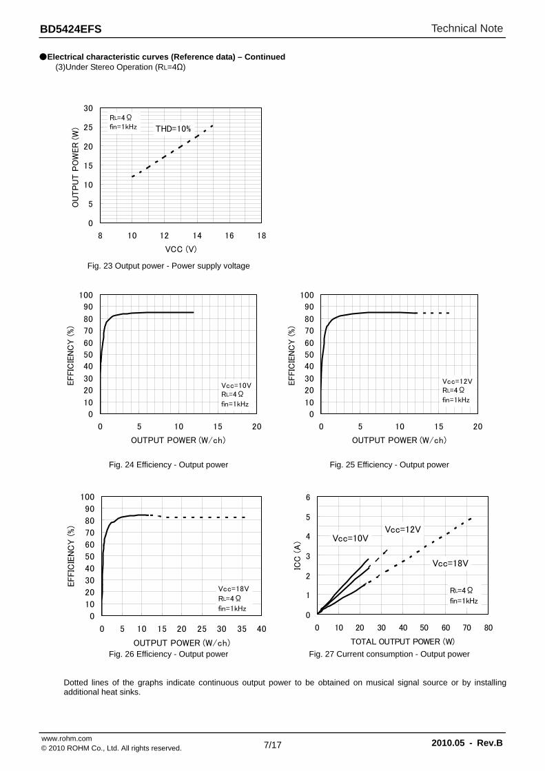
Electrical characteristic curves (Reference data) – Continued (3)Under Stereo Operation (RL=4Ω)
Fig. 23 Output power - Power supply voltage
Fig. 24 Efficiency - Output power Fig. 25 Efficiency - Output power
Fig. 26 Efficiency - Output power Fig. 27 Current consumption - Output power
Dotted lines of the graphs indicate continuous output power to be obtained on musical signal source or by installing additional heat sinks.
Technical Note
www.rohm.com 2010.05 - Rev.B© 2010 ROHM Co., Ltd. All rights reserved.
8/17
BD5424EFS
BD5424EFS
(MAX 18.85 include BURR)
18.5±0.1
Lot No.
TYPE
1PIN MARK
(6.0)
(5.0
)
0.85
44 23
1 22
1.0
MA
X
(Unit: mm)
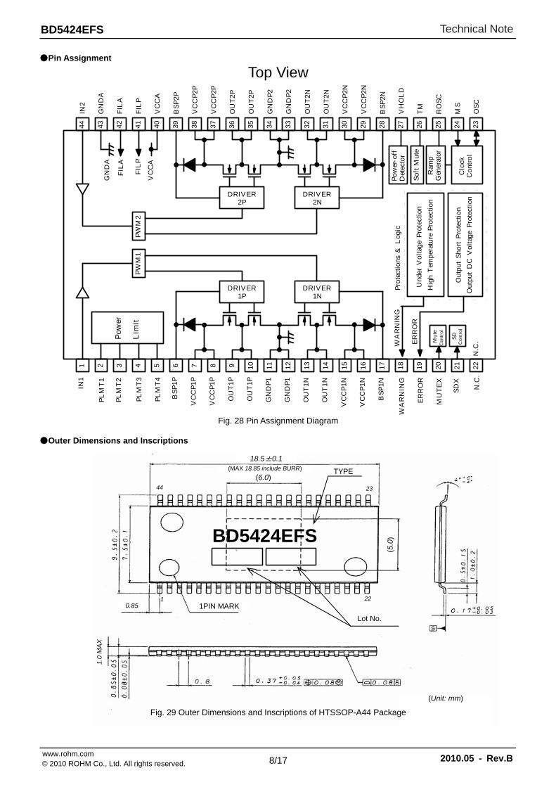
Pin Assignment
Top View
IN1
PL
MT
1
PL
MT
2
BS
P1
P
VC
CP
1P
VC
CP
1P
OU
T1
P
OU
T1
P
GN
DP
1
GN
DP
1
OU
T1
N
OU
T1
N
VC
CP
1N
BS
P1N
WA
RN
ING
ER
RO
R
MU
TE
X
N.C
.
IN2
GN
DA
FIL
A
FIL
P
VC
CA
BS
P2
P
VC
CP
2P
VC
CP
2P
OU
T2
P
OU
T2
P
GN
DP
2
GN
DP
2
OU
T2N
OU
T2N
VC
CP
2N
VC
CP
2N
BS
P2N
VH
OL
D
TM
RO
SC
MS
OS
C
VC
CP
1N
Ou
tpu
tD
CV
olt
age
Pro
tect
ion
Ou
tpu
tS
hort
Pro
tect
ion
7 8 9 1062 3 4 51 11 12 13 14 15 16 17 18 19 20 21 22
25 24 2328 27 2630 293132333435363738394041424344
DRIVER1P
DRIVER1N
Pow
er
Lim
it
So
ftM
ute
FIL
PP
WM
1P
WM
2
DRIVER2P
DRIVER2N
FIL
A
ER
RO
R
Mu
teC
ontr
ol
Und
erV
olt
age
Pro
tect
ion
Hig
hT
empe
ratu
reP
rote
ctio
nR
amp
Gen
erat
or
Clo
ckC
on
tro
lN
.C.
Pro
tect
ion
s&
Log
icP
ow
er-o
ffD
etec
tor
VC
CA
GN
DA
WA
RN
ING
PL
MT
3
PL
MT
4
Con
tro
lS
DS
DX
Fig. 28 Pin Assignment Diagram
Outer Dimensions and Inscriptions
Fig. 29 Outer Dimensions and Inscriptions of HTSSOP-A44 Package
Technical Note
www.rohm.com 2010.05 - Rev.B© 2010 ROHM Co., Ltd. All rights reserved.
9/17
BD5424EFS
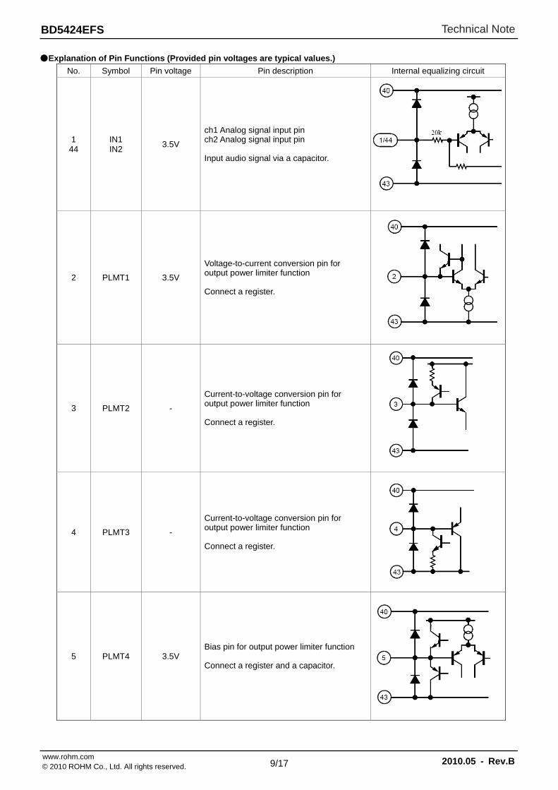
Explanation of Pin Functions (Provided pin voltages are typical values.)
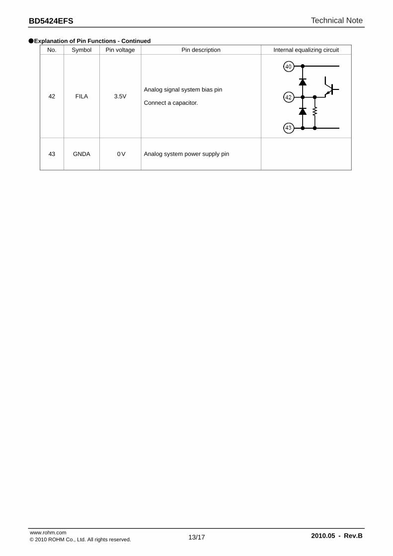
No. Symbol Pin voltage Pin description Internal equalizing circuit
1 44
IN1 IN2 3.5V
ch1 Analog signal input pin ch2 Analog signal input pin Input audio signal via a capacitor.
2 PLMT1 3.5V Voltage-to-current conversion pin for output power limiter function Connect a register.
3 PLMT2 - Current-to-voltage conversion pin for output power limiter function Connect a register.
4 PLMT3 - Current-to-voltage conversion pin for output power limiter function Connect a register.
5 PLMT4 3.5V Bias pin for output power limiter function Connect a register and a capacitor.
Technical Note
www.rohm.com 2010.05 - Rev.B© 2010 ROHM Co., Ltd. All rights reserved.
10/17
BD5424EFS
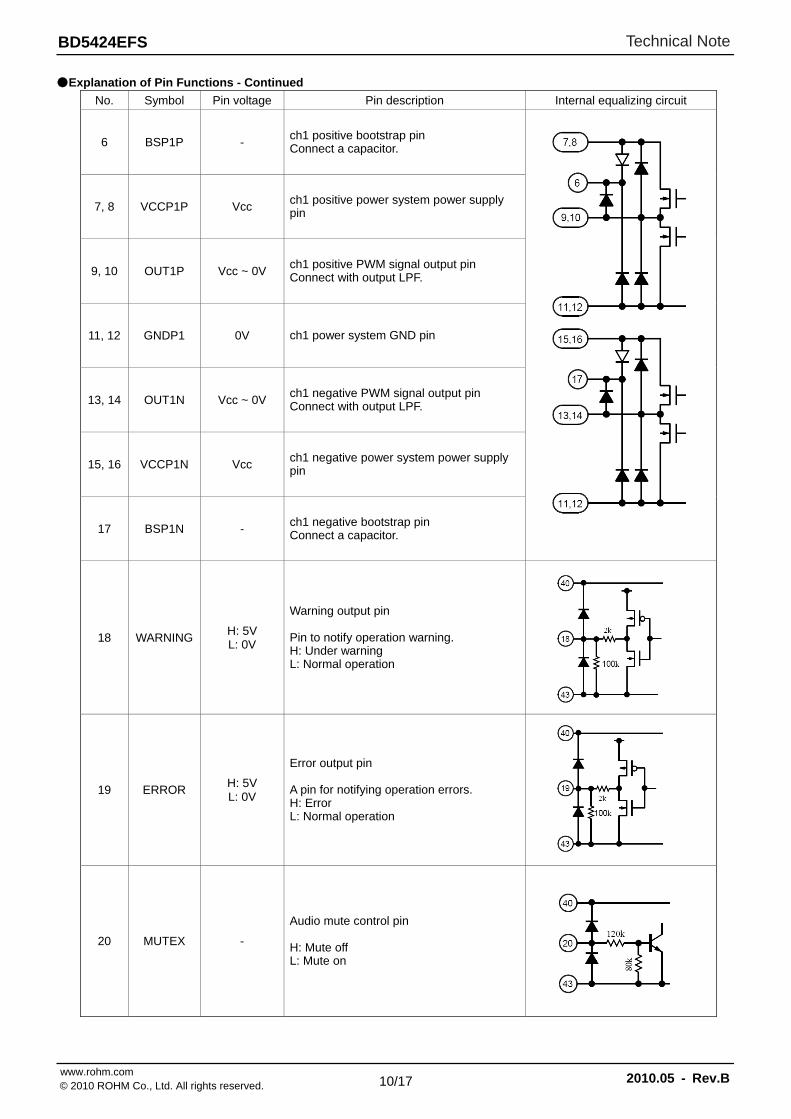
Explanation of Pin Functions - Continued
No. Symbol Pin voltage Pin description Internal equalizing circuit
6 BSP1P - ch1 positive bootstrap pin Connect a capacitor.
7, 8 VCCP1P Vcc ch1 positive power system power supply pin
9, 10 OUT1P Vcc ~ 0V ch1 positive PWM signal output pin Connect with output LPF.
11, 12 GNDP1 0V ch1 power system GND pin
13, 14 OUT1N Vcc ~ 0V ch1 negative PWM signal output pin Connect with output LPF.
15, 16 VCCP1N Vcc ch1 negative power system power supply pin
17 BSP1N - ch1 negative bootstrap pin Connect a capacitor.
18 WARNING H: 5V L: 0V
Warning output pin Pin to notify operation warning. H: Under warning L: Normal operation
19 ERROR H: 5V L: 0V
Error output pin A pin for notifying operation errors. H: Error L: Normal operation
20 MUTEX - Audio mute control pin H: Mute off L: Mute on
Technical Note
www.rohm.com 2010.05 - Rev.B© 2010 ROHM Co., Ltd. All rights reserved.
11/17
BD5424EFS
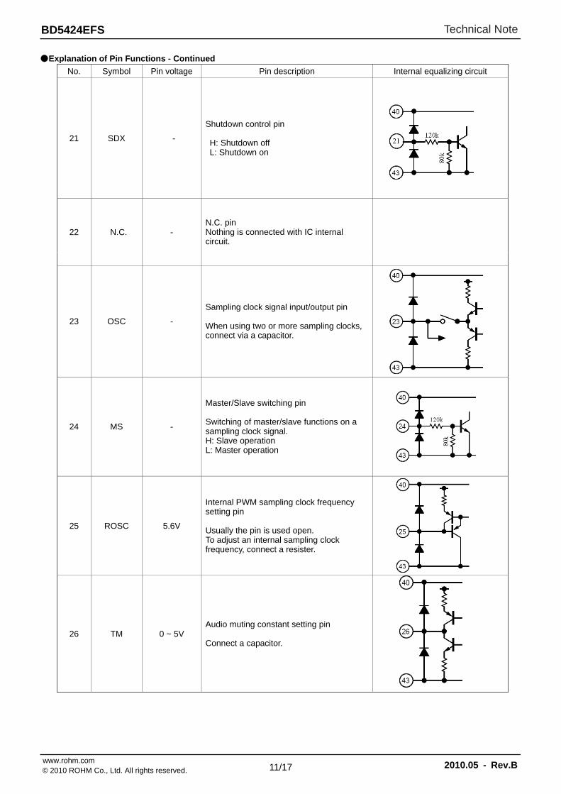
Explanation of Pin Functions - Continued
No. Symbol Pin voltage Pin description Internal equalizing circuit
21 SDX - Shutdown control pin H: Shutdown off L: Shutdown on
22 N.C. - N.C. pin Nothing is connected with IC internal circuit.
23 OSC - Sampling clock signal input/output pin When using two or more sampling clocks, connect via a capacitor.
24 MS -
Master/Slave switching pin Switching of master/slave functions on a sampling clock signal. H: Slave operation L: Master operation
25 ROSC 5.6V
Internal PWM sampling clock frequency setting pin Usually the pin is used open. To adjust an internal sampling clock frequency, connect a resister.
26 TM 0 ~ 5V Audio muting constant setting pin Connect a capacitor.
Technical Note
www.rohm.com 2010.05 - Rev.B© 2010 ROHM Co., Ltd. All rights reserved.
12/17
BD5424EFS
Explanation of Pin Functions - Continued
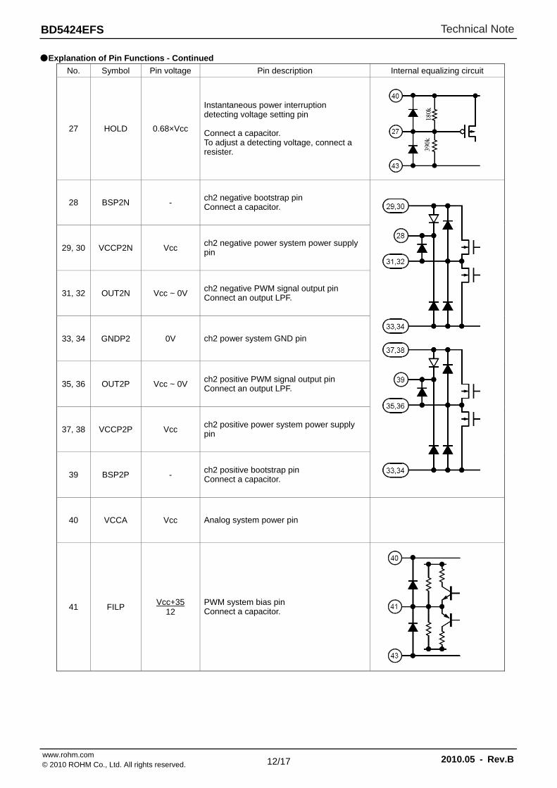
No. Symbol Pin voltage Pin description Internal equalizing circuit
27 HOLD 0.68×Vcc
Instantaneous power interruption detecting voltage setting pin Connect a capacitor. To adjust a detecting voltage, connect a resister.
28 BSP2N - ch2 negative bootstrap pin Connect a capacitor.
29, 30 VCCP2N Vcc ch2 negative power system power supply pin
31, 32 OUT2N Vcc ~ 0V ch2 negative PWM signal output pin Connect an output LPF.
33, 34 GNDP2 0V ch2 power system GND pin
35, 36 OUT2P Vcc ~ 0V ch2 positive PWM signal output pin Connect an output LPF.
37, 38 VCCP2P Vcc ch2 positive power system power supply pin
39 BSP2P - ch2 positive bootstrap pin Connect a capacitor.
40 VCCA Vcc Analog system power pin
41 FILP Vcc+35
12 PWM system bias pin Connect a capacitor.
Technical Note
www.rohm.com 2010.05 - Rev.B© 2010 ROHM Co., Ltd. All rights reserved.
13/17
BD5424EFS
Explanation of Pin Functions - Continued
No. Symbol Pin voltage Pin description Internal equalizing circuit
42 FILA 3.5V Analog signal system bias pin Connect a capacitor.
43 GNDA 0V Analog system power supply pin
Technical Note
www.rohm.com 2010.05 - Rev.B© 2010 ROHM Co., Ltd. All rights reserved.
14/17
BD5424EFS
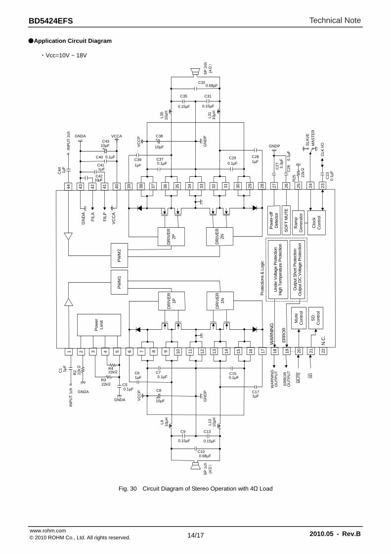
Application Circuit Diagram
・Vcc=10V ~ 18V
GNDA VCCA
INP
UT
2ch
1µF
10µF
10µF
MU
TE
WA
RN
ING
OU
TP
UT
SLA
VE
MA
ST
ER
CL
K I/
O
R25
ER
RO
RO
UT
PU
T
INP
UT
1ch
0.1
µF
GNDP
0.1µF
22kΩ
22kΩ
22kΩ
GNDA
GNDA
0.1µF
SD
1 2 3 4 5 6 7 8 9 14 15 16 17 18 19 20 21 22
36 35 34 33 32 31
30 29 28 27 26 25
44 43
42 41 40 39
10 11 12 13
38 37 24 23
PW
M1
DR
IVE
R1P
SO
FT
MU
TE
DR
IVE
R1N
PW
M2
DR
IVE
R2P
FIL
P
DR
IVE
R2N
Clo
ckC
ont
rol
Mu
teC
ont
rol
ER
RO
R
Ram
pG
ener
ato
r
GN
DA
VC
CA
WA
RN
ING
FIL
A
Pro
tect
ions
& L
ogic
Und
er V
olta
ge P
rote
ctio
nH
igh
Tem
pera
ture
Pro
tect
ion
Out
put S
hort
Pro
tect
ion
Out
put D
C V
olta
ge P
rote
ctio
n
N.C
.
Po
wer
Lim
it SD
Co
ntro
l
Pow
er-o
ffD
etec
tor
C43
1µF
R2
C40
C41
C42
C2
6
22k
Ω
0.1
µF
C2
3
3.3
µF
C2
7
R4
R3C5
+
0.1µF
VC
CP
GN
DP
1µF+
10µF
C38
C29 C28
0.1µFC37
1µF
C39
SP
2ch
(4Ω
)
0.15µF 0.15µF
10µ
H
10µ
H
C35
C320.68µF
C31
L31
L35
0.1µF
VC
CP
GN
DP
1µF+
10µF
C8
C15
C17
0.1µFC7
1µFC6
SP
1ch
(4Ω
)
0.15µF 0.15µF
10µ
H
10µ
H
C9
C100.68µF
C13
L13
L9
1µF
C44
C1
Fig. 30 Circuit Diagram of Stereo Operation with 4Ω Load
Technical Note
www.rohm.com 2010.05 - Rev.B© 2010 ROHM Co., Ltd. All rights reserved.
15/17
BD5424EFS
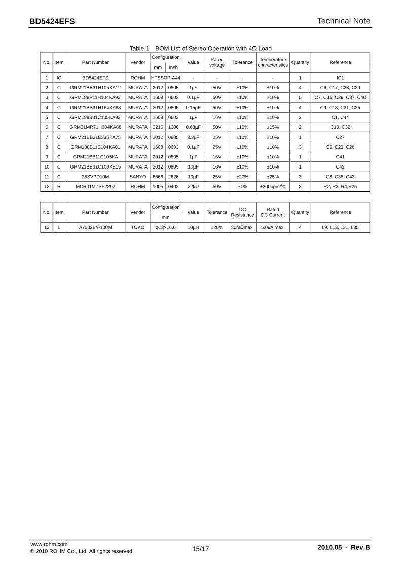
Table 1 BOM List of Stereo Operation with 4Ω Load
No. Item Part Number Vendor Configuration
Value Rated voltage
ToleranceTemperature
characteristics Quantity Reference
mm inch
1 IC BD5424EFS ROHM HTSSOP-A44 - - - - 1 IC1
2 C GRM21BB31H105KA12 MURATA 2012 0805 1µF 50V ±10% ±10% 4 C6, C17, C28, C39
3 C GRM188R11H104KA93 MURATA 1608 0603 0.1µF 50V ±10% ±10% 5 C7, C15, C29, C37, C40
4 C GRM21BB31H154KA88 MURATA 2012 0805 0.15µF 50V ±10% ±10% 4 C9, C13, C31, C35
5 C GRM188B31C105KA92 MURATA 1608 0603 1µF 16V ±10% ±10% 2 C1, C44
6 C GRM31MR71H684KA88 MURATA 3216 1206 0.68µF 50V ±10% ±15% 2 C10, C32
7 C GRM21BB31E335KA75 MURATA 2012 0805 3.3µF 25V ±10% ±10% 1 C27
8 C GRM188B11E104KA01 MURATA 1608 0603 0.1µF 25V ±10% ±10% 3 C5, C23, C26
9 C GRM21BB11C105KA MURATA 2012 0805 1µF 16V ±10% ±10% 1 C41
10 C GRM21BB31C106KE15 MURATA 2012 0805 10µF 16V ±10% ±10% 1 C42
11 C 25SVPD10M SANYO 6666 2626 10µF 25V ±20% ±25% 3 C8, C38, C43
12 R MCR01MZPF2202 ROHM 1005 0402 22kΩ 50V ±1% ±200ppm/ 3 R2, R3, R4,R25
No. Item Part Number Vendor Configuration
Value ToleranceDC
ResistanceRated
DC Current Quantity Reference
mm
13 L A7502BY-100M TOKO φ13×16.0 10µH ±20% 30mΩmax. 5.09A max. 4 L9, L13, L31, L35
Technical Note
www.rohm.com 2010.05 - Rev.B© 2010 ROHM Co., Ltd. All rights reserved.
16/17
BD5424EFS
Notes for use Notes for use 1. About absolute maximum ratings
If an applied voltage or an operating temperature exceeds an absolute maximum rating, it may cause destruction of a device. A result of destruction, whether it is short mode or open mode, is not predictable. Therefore, provide a physical safety measure such as fuse, against a special mode that may violate conditions of absolute maximum ratings.
2. About power supply line As return of current regenerated by back EMF of output coil happens, take steps such as putting capacitor between power supply and GND as a electric pathway for the regenerated current. Be sure that there is no problem with each property such as emptied capacity at lower temperature regarding electrolytic capacitor to decide capacity value. If the connected power supply does not have sufficient current absorption capacity, regenerative current will cause the voltage on the power supply line to rise, which combined with the product and its peripheral circuitry may exceed the absolute maximum ratings. It is recommended to implement a physical safety measure such as the insertion of a voltage clamp diode between the power supply and GND pins.
3. Potential of GND (11, 12, 33, 34, and 43 pins) Potential of the GND terminal must be the lowest under any operating conditions.
4. About thermal design Perform thermal design with sufficient margins, in consideration of maximum power dissipation Pd under actual operating conditions. This product has an exposed frame on the back of the package, and it is assumed that the frame is used with measures to improve efficiency of heat dissipation. In addition to front surface of board, provide a heat dissipation pattern as widely as possible on the back also. A class-D power amplifier has heat dissipation efficiency far higher than that of conventional analog power amplifier and generates less heat. However, extra attention must be paid in thermal design so that a power dissipation Pdiss should not exceed the maximum power dissipation Pd.
Maximum power dissipation W θ
Ta-TPd
aj
jmax Tjmax: Maximum temperature junction = 150[]
Ta: Operating ambient temperature [] θja: Package thermal resistance [/W] Po: Output power [W] η: Efficiency
Power dissipation W 1-η
1PP Odiss
5. About operations in strong electric field
Note that the device may malfunction in a strong electric field.
6. Thermal shutdown (TSD) circuit This product is provided with a built-in thermal shutdown circuit. When the thermal shutdown circuit operates, the output transistors are placed under open status. The thermal shutdown circuit is primarily intended to shut down the IC avoiding thermal runaway under abnormal conditions with a chip temperature exceeding Tjmax = 150.
7. About shorting between pins and installation failure
Be careful about direction and displacement of an LSI when installing it onto the board. Faulty installation may destroy the LSI when the device is energized. In addition, a foreign matter getting in between LSI pins, pins and power supply, and pins and GND may cause shorting and destruction of the LSI.
8. About power supply startup and shutdown When starting up a power supply, be sure to place the MUTEX pin (pin 20) and SDX pin (pin 21), at “L” level. When shutting down a power supply also, be sure to place the pin at “L” level. Those processes reduce pop noises generated upon turning on and off the power supply. In addition, all power supply pins must be started up and shut down at the same time.
9. About WARNING output pin (pin 18) and ERROR output pin (pin 19) A WARNING flag is output from the WARNING output pin upon operation of the high-temperature protection function and under-voltage protection function. And an ERROR flag is output from the ERROR output pin upon operation of VCC/GND shorting protection function and speaker DC voltage applying protection function. These flags are the function which the condition of this product is shown in. The use which aimed at the protection except for this product is prohibition.
10. About N.C. pins (pin 22) The N.C. (Non connection) pins are not connected with an internal circuit. Leave the pins open or connect them to GND.
Technical Note
www.rohm.com 2010.05 - Rev.B© 2010 ROHM Co., Ltd. All rights reserved.
17/17
BD5424EFS
Ordering part number
B D 5 4 2 4 E F S - E 2
Part No.
Part No.
Package EFS:HTSSOP-44
Packaging and forming specification E2: Embossed tape and reel
∗ Order quantity needs to be multiple of the minimum quantity.
<Tape and Reel information>
Embossed carrier tape (with dry pack)Tape
Quantity
Direction of feed
The direction is the 1pin of product is at the upper left when you hold reel on the left hand and you pull out the tape on the right hand
1500pcs
E2
( )
Direction of feed
Reel1pin
(Unit : mm)
HTSSOP-A44(5
.0)
(6.0)
0.85
9.5±
0.2
7.5±
0.1
44 23
221
(MAX 18.85 include BURR)18.5±0.1
1PIN MARK
0.8
1.0M
AX
0.85
±0.0
5
0.08
±0.0
5
0.08 M0.37+0.05-0.04
S0.08
0.5±
0.15
1.0±
0.2
0.17+0.05-0.03
S
4°+6°−4°
DatasheetDatasheet
Notice - GE Rev.002© 2014 ROHM Co., Ltd. All rights reserved.
Notice Precaution on using ROHM Products
1. Our Products are designed and manufactured for application in ordinary electronic equipments (such as AV equipment, OA equipment, telecommunication equipment, home electronic appliances, amusement equipment, etc.). If you intend to use our Products in devices requiring extremely high reliability (such as medical equipment (Note 1), transport equipment, traffic equipment, aircraft/spacecraft, nuclear power controllers, fuel controllers, car equipment including car accessories, safety devices, etc.) and whose malfunction or failure may cause loss of human life, bodily injury or serious damage to property (“Specific Applications”), please consult with the ROHM sales representative in advance. Unless otherwise agreed in writing by ROHM in advance, ROHM shall not be in any way responsible or liable for any damages, expenses or losses incurred by you or third parties arising from the use of any ROHM’s Products for Specific Applications.
(Note1) Medical Equipment Classification of the Specific Applications JAPAN USA EU CHINA
CLASSⅢ CLASSⅢ
CLASSⅡb CLASSⅢ
CLASSⅣ CLASSⅢ
2. ROHM designs and manufactures its Products subject to strict quality control system. However, semiconductor
products can fail or malfunction at a certain rate. Please be sure to implement, at your own responsibilities, adequate safety measures including but not limited to fail-safe design against the physical injury, damage to any property, which a failure or malfunction of our Products may cause. The following are examples of safety measures:
[a] Installation of protection circuits or other protective devices to improve system safety [b] Installation of redundant circuits to reduce the impact of single or multiple circuit failure
3. Our Products are designed and manufactured for use under standard conditions and not under any special or extraordinary environments or conditions, as exemplified below. Accordingly, ROHM shall not be in any way responsible or liable for any damages, expenses or losses arising from the use of any ROHM’s Products under any special or extraordinary environments or conditions. If you intend to use our Products under any special or extraordinary environments or conditions (as exemplified below), your independent verification and confirmation of product performance, reliability, etc, prior to use, must be necessary:
[a] Use of our Products in any types of liquid, including water, oils, chemicals, and organic solvents [b] Use of our Products outdoors or in places where the Products are exposed to direct sunlight or dust [c] Use of our Products in places where the Products are exposed to sea wind or corrosive gases, including Cl2,
H2S, NH3, SO2, and NO2
[d] Use of our Products in places where the Products are exposed to static electricity or electromagnetic waves [e] Use of our Products in proximity to heat-producing components, plastic cords, or other flammable items [f] Sealing or coating our Products with resin or other coating materials [g] Use of our Products without cleaning residue of flux (even if you use no-clean type fluxes, cleaning residue of
flux is recommended); or Washing our Products by using water or water-soluble cleaning agents for cleaning residue after soldering
[h] Use of the Products in places subject to dew condensation
4. The Products are not subject to radiation-proof design. 5. Please verify and confirm characteristics of the final or mounted products in using the Products. 6. In particular, if a transient load (a large amount of load applied in a short period of time, such as pulse. is applied,
confirmation of performance characteristics after on-board mounting is strongly recommended. Avoid applying power exceeding normal rated power; exceeding the power rating under steady-state loading condition may negatively affect product performance and reliability.
7. De-rate Power Dissipation (Pd) depending on Ambient temperature (Ta). When used in sealed area, confirm the actual
ambient temperature. 8. Confirm that operation temperature is within the specified range described in the product specification. 9. ROHM shall not be in any way responsible or liable for failure induced under deviant condition from what is defined in
this document.
Precaution for Mounting / Circuit board design 1. When a highly active halogenous (chlorine, bromine, etc.) flux is used, the residue of flux may negatively affect product
performance and reliability. 2. In principle, the reflow soldering method must be used; if flow soldering method is preferred, please consult with the
ROHM representative in advance. For details, please refer to ROHM Mounting specification

DatasheetDatasheet
Notice - GE Rev.002© 2014 ROHM Co., Ltd. All rights reserved.
Precautions Regarding Application Examples and External Circuits 1. If change is made to the constant of an external circuit, please allow a sufficient margin considering variations of the
characteristics of the Products and external components, including transient characteristics, as well as static characteristics.
2. You agree that application notes, reference designs, and associated data and information contained in this document
are presented only as guidance for Products use. Therefore, in case you use such information, you are solely responsible for it and you must exercise your own independent verification and judgment in the use of such information contained in this document. ROHM shall not be in any way responsible or liable for any damages, expenses or losses incurred by you or third parties arising from the use of such information.
Precaution for Electrostatic
This Product is electrostatic sensitive product, which may be damaged due to electrostatic discharge. Please take proper caution in your manufacturing process and storage so that voltage exceeding the Products maximum rating will not be applied to Products. Please take special care under dry condition (e.g. Grounding of human body / equipment / solder iron, isolation from charged objects, setting of Ionizer, friction prevention and temperature / humidity control).
Precaution for Storage / Transportation 1. Product performance and soldered connections may deteriorate if the Products are stored in the places where:
[a] the Products are exposed to sea winds or corrosive gases, including Cl2, H2S, NH3, SO2, and NO2 [b] the temperature or humidity exceeds those recommended by ROHM [c] the Products are exposed to direct sunshine or condensation [d] the Products are exposed to high Electrostatic
2. Even under ROHM recommended storage condition, solderability of products out of recommended storage time period may be degraded. It is strongly recommended to confirm solderability before using Products of which storage time is exceeding the recommended storage time period.
3. Store / transport cartons in the correct direction, which is indicated on a carton with a symbol. Otherwise bent leads
may occur due to excessive stress applied when dropping of a carton. 4. Use Products within the specified time after opening a humidity barrier bag. Baking is required before using Products of
which storage time is exceeding the recommended storage time period.
Precaution for Product Label QR code printed on ROHM Products label is for ROHM’s internal use only.
Precaution for Disposition When disposing Products please dispose them properly using an authorized industry waste company.
Precaution for Foreign Exchange and Foreign Trade act Since our Products might fall under controlled goods prescribed by the applicable foreign exchange and foreign trade act, please consult with ROHM representative in case of export.
Precaution Regarding Intellectual Property Rights 1. All information and data including but not limited to application example contained in this document is for reference
only. ROHM does not warrant that foregoing information or data will not infringe any intellectual property rights or any other rights of any third party regarding such information or data. ROHM shall not be in any way responsible or liable for infringement of any intellectual property rights or other damages arising from use of such information or data.:
2. No license, expressly or implied, is granted hereby under any intellectual property rights or other rights of ROHM or any
third parties with respect to the information contained in this document.
Other Precaution 1. This document may not be reprinted or reproduced, in whole or in part, without prior written consent of ROHM. 2. The Products may not be disassembled, converted, modified, reproduced or otherwise changed without prior written
consent of ROHM. 3. In no event shall you use in any way whatsoever the Products and the related technical information contained in the
Products or this document for any military purposes, including but not limited to, the development of mass-destruction weapons.
4. The proper names of companies or products described in this document are trademarks or registered trademarks of
ROHM, its affiliated companies or third parties.

DatasheetDatasheet
Notice – WE Rev.001© 2014 ROHM Co., Ltd. All rights reserved.
General Precaution 1. Before you use our Pro ducts, you are requested to care fully read this document and fully understand its contents.
ROHM shall n ot be in an y way responsible or liabl e for fa ilure, malfunction or acci dent arising from the use of a ny ROHM’s Products against warning, caution or note contained in this document.
2. All information contained in this docume nt is current as of the issuing date and subj ect to change without any prior
notice. Before purchasing or using ROHM’s Products, please confirm the la test information with a ROHM sale s representative.
3. The information contained in this doc ument is provi ded on an “as is” basis and ROHM does not warrant that all
information contained in this document is accurate an d/or error-free. ROHM shall not be in an y way responsible or liable for any damages, expenses or losses incurred by you or third parties resulting from inaccuracy or errors of or concerning such information.


![Speaker Protection C1237 User Manual - Analog Metricanalogmetric.com/download/Speaker Protection C1237 User Manual.pdf[SPEAKER PROTECTION C1237 USE R MANUAL ] Analog Metric Page 2](https://img.pdfslide.net/doc/110x75/60801e287f78984612319a54/speaker-protection-c1237-user-manual-analog-protection-c1237-user-manualpdf-speaker.jpg)