Embed Size (px)
Citation preview
Document Number: MD00047Revision 5.06
March 05, 2011
MIPS Technologies, Inc.955 East Arques Avenue
Sunnyvale, CA 94085-4521
Copyright © 2000-2010 MIPS Technologies Inc. All rights reserved.
MIPS® EJTAG Specification
MIPS® EJTAG Specification, Revision 5.06
Copyright © 2000-2010 MIPS Technologies Inc. All rights reserved.
Template: nB1.03, Built with tags: 2B
Copyright © 2000-2010 MIPS Technologies, Inc. All rights reserved.
Unpublished rights (if any) reserved under the copyright laws of the United States of America and other countries.
This document contains information that is proprietary to MIPS Technologies, Inc. ("MIPS Technologies"). Any copying, reproducing, modifying or use ofthis information (in whole or in part) that is not expressly permitted in writing by MIPS Technologies or an authorized third party is strictly prohibited. At aminimum, this information is protected under unfair competition and copyright laws. Violations thereof may result in criminal penalties and fines.
Any document provided in source format (i.e., in a modifiable form such as in FrameMaker or Microsoft Word format) is subject to use and distributionrestrictions that are independent of and supplemental to any and all confidentiality restrictions. UNDER NO CIRCUMSTANCES MAY A DOCUMENTPROVIDED IN SOURCE FORMAT BE DISTRIBUTED TO A THIRD PARTY IN SOURCE FORMAT WITHOUT THE EXPRESS WRITTENPERMISSION OF MIPS TECHNOLOGIES, INC.
MIPS Technologies reserves the right to change the information contained in this document to improve function, design or otherwise. MIPS Technologies doesnot assume any liability arising out of the application or use of this information, or of any error or omission in such information. Any warranties, whetherexpress, statutory, implied or otherwise, including but not limited to the implied warranties of merchantability or fitness for a particular purpose, are excluded.Except as expressly provided in any written license agreement from MIPS Technologies or an authorized third party, the furnishing of this document does notgive recipient any license to any intellectual property rights, including any patent rights, that cover the information in this document.
The information contained in this document shall not be exported, reexported, transferred, or released, directly or indirectly, in violation of the law of anycountry or international law, regulation, treaty, Executive Order, statute, amendments or supplements thereto. Should a conflict arise regarding the export,reexport, transfer, or release of the information contained in this document, the laws of the United States of America shall be the governing law.
The information contained in this document constitutes one or more of the following: commercial computer software, commercial computer softwaredocumentation or other commercial items. If the user of this information, or any related documentation of any kind, including related technical data or manuals,is an agency, department, or other entity of the United States government ("Government"), the use, duplication, reproduction, release, modification, disclosure,or transfer of this information, or any related documentation of any kind, is restricted in accordance with Federal Acquisition Regulation 12.212 for civilianagencies and Defense Federal Acquisition Regulation Supplement 227.7202 for military agencies. The use of this information by the Government is furtherrestricted in accordance with the terms of the license agreement(s) and/or applicable contract terms and conditions covering this information from MIPSTechnologies or an authorized third party.
MIPS, MIPS I, MIPS II, MIPS III, MIPS IV, MIPS V, MIPSr3, MIPS32, MIPS64, microMIPS32, microMIPS64, MIPS-3D, MIPS16, MIPS16e, MIPS-Based,MIPSsim, MIPSpro, MIPS Technologies logo, MIPS-VERIFIED, MIPS-VERIFIED logo, 4K, 4Kc, 4Km, 4Kp, 4KE, 4KEc, 4KEm, 4KEp, 4KS, 4KSc, 4KSd,M4K, M14K, 5K, 5Kc, 5Kf, 24K, 24Kc, 24Kf, 24KE, 24KEc, 24KEf, 34K, 34Kc, 34Kf, 74K, 74Kc, 74Kf, 1004K, 1004Kc, 1004Kf, 1074K, 1074Kc, 1074Kf,R3000, R4000, R5000, ASMACRO, Atlas, "At the core of the user experience.", BusBridge, Bus Navigator, CLAM, CorExtend, CoreFPGA, CoreLV, EC,FPGA View, FS2, FS2 FIRST SILICON SOLUTIONS logo, FS2 NAVIGATOR, HyperDebug, HyperJTAG, JALGO, Logic Navigator, Malta, MDMX, MED,MGB, microMIPS, OCI, PDtrace, the Pipeline, Pro Series, SEAD, SEAD-2, SmartMIPS, SOC-it, System Navigator, and YAMON are trademarks or registeredtrademarks of MIPS Technologies, Inc. in the United States and other countries.
All other trademarks referred to herein are the property of their respective owners.
MIPS® EJTAG Specification, Revision 5.06 3
Copyright © 2000-2010 MIPS Technologies Inc. All rights reserved.
Table of Contents
Chapter 1: Overview of the EJTAG System ....................................................................................... 131.1: Introduction to EJTAG ............................................................................................................................... 131.2: Historical Perspective ................................................................................................................................ 141.3: EJTAG Capabilities ................................................................................................................................... 17
1.3.1: Debug Exception and Debug Mode ................................................................................................. 171.3.2: Off-board EJTAG Memory ............................................................................................................... 171.3.3: Debug Breakpoint Instruction........................................................................................................... 181.3.4: Hardware Breakpoints...................................................................................................................... 181.3.5: Single-Step Execution...................................................................................................................... 18
1.4: EJTAG Components and Options ............................................................................................................. 181.4.1: EJTAG Processor Core Extensions ................................................................................................. 191.4.2: EJTAG Test Access Port ................................................................................................................. 201.4.3: Debug Control Register.................................................................................................................... 201.4.4: Hardware Breakpoint Unit ................................................................................................................ 201.4.5: Fast Debug Channel ........................................................................................................................ 21
1.5: Complex Breakpoint and Trigger (CBT) Block .......................................................................................... 211.6: EJTAG-Specific Coprocessor 0 Registers................................................................................................. 211.7: Memory-Mapped EJTAG Registers........................................................................................................... 22
1.7.1: Debug Control Register.................................................................................................................... 221.7.2: Debug Exception Vector Location.................................................................................................... 221.7.3: Load Data Value Register ................................................................................................................ 231.7.4: Instruction Hardware Breakpoint Registers...................................................................................... 231.7.5: Data Hardware Breakpoint Registers............................................................................................... 241.7.6: Complex Break and Trigger Registers ............................................................................................. 24
1.8: Memory-Mapped EJTAG Memory Segment ............................................................................................. 251.9: Memory-Mapped Fast Debug Channel Registers ..................................................................................... 251.10: EJTAG Test Access Port Registers......................................................................................................... 261.11: The Implications of Multiprocessing and Multithreading for EJTAG ........................................................ 271.12: Related Documents ................................................................................................................................. 271.13: Notations and Conventions ..................................................................................................................... 28
1.13.1: Compliance .................................................................................................................................... 281.13.2: UNPREDICTABLE and UNDEFINED Operations ......................................................................... 281.13.3: Register Field Notations................................................................................................................. 291.13.4: Value Notations.............................................................................................................................. 301.13.5: Address Notations.......................................................................................................................... 30
Chapter 2: EJTAG Processor Core Extensions ................................................................................. 312.1: Overview.................................................................................................................................................... 312.2: Debug Mode Execution ............................................................................................................................. 32
2.2.1: Debug Mode Instruction Set............................................................................................................. 322.2.2: Debug Mode Address Space ........................................................................................................... 322.2.3: Debug Mode Handling of Processor Resources .............................................................................. 372.2.4: CP0 and dseg Segment Hazards..................................................................................................... 39
2.3: Debug Exceptions ..................................................................................................................................... 412.3.1: Debug Exception Priorities............................................................................................................... 412.3.2: Debug Exception Vector Location.................................................................................................... 422.3.3: Debug Exception ISA mode............................................................................................................. 43
4 MIPS® EJTAG Specification, Revision 5.06
Copyright © 2000-2010 MIPS Technologies Inc. All rights reserved.
2.3.4: General Debug Exception Processing ............................................................................................. 442.3.5: Debug Breakpoint Exception............................................................................................................ 452.3.6: Debug Instruction Break Exception.................................................................................................. 462.3.7: Debug Data Break Load/Store Exception ........................................................................................ 462.3.8: Debug Data Break Load/Store Imprecise Exception........................................................................ 462.3.9: Debug Single Step Exception .......................................................................................................... 472.3.10: Debug Interrupt Exception ............................................................................................................. 49
2.4: Debug Mode Exceptions ........................................................................................................................... 502.4.1: Exceptions Taken in Debug Mode ................................................................................................... 512.4.2: Exceptions on Imprecise Errors ....................................................................................................... 522.4.3: Debug Mode Exception Processing ................................................................................................. 52
2.5: Interrupts and NMIs ................................................................................................................................... 532.5.1: Interrupts .......................................................................................................................................... 542.5.2: NMIs................................................................................................................................................. 54
2.6: Reset and Soft Reset of Processor ........................................................................................................... 542.6.1: EJTAGBOOT Feature ...................................................................................................................... 542.6.2: Reset from Probe............................................................................................................................. 552.6.3: Processor Reset by Probe through Test Access Port...................................................................... 552.6.4: Reset Occurred Indication through Test Access Port ...................................................................... 552.6.5: Soft Reset Enable ............................................................................................................................ 552.6.6: Reset of Other Debug Features ....................................................................................................... 55
2.7: EJTAG Coprocessor 0 Registers .............................................................................................................. 552.7.1: Debug Register (CP0 Register 23, Select 0) ................................................................................... 562.7.2: Debug2 Register (CP0 Register 23, Select 6) ................................................................................. 652.7.3: Debug Exception Program Counter Register (CP0 Register 24, Select 0) ...................................... 662.7.4: Debug Exception Save Register (CP0 Register 31, Select 0) ......................................................... 67
2.8: EJTAG Instructions.................................................................................................................................... 67
Chapter 3: Debug Control Register..................................................................................................... 75
Chapter 4: EJTAG Test Access Port ................................................................................................... 814.1: TAP Overview............................................................................................................................................ 814.2: TAP Signals............................................................................................................................................... 82
4.2.1: Test Clock Input (TCK)..................................................................................................................... 824.2.2: Test Mode Select Input (TMS) ......................................................................................................... 824.2.3: Test Data Input (TDI) ....................................................................................................................... 834.2.4: Test Data Output (TDO)................................................................................................................... 834.2.5: Test Reset Input (TRST*)................................................................................................................. 83
4.3: TAP Controller ........................................................................................................................................... 834.3.1: Test-Logic-Reset State .................................................................................................................... 844.3.2: Capture-IR State .............................................................................................................................. 844.3.3: Shift-IR State.................................................................................................................................... 844.3.4: Update-IR State ............................................................................................................................... 854.3.5: Capture-DR State............................................................................................................................. 854.3.6: Shift-DR State .................................................................................................................................. 854.3.7: Update-DR State.............................................................................................................................. 85
4.4: Instruction Register and Special Instructions ............................................................................................ 854.4.1: ALL Instruction ................................................................................................................................. 864.4.2: EJTAGBOOT and NORMALBOOT Instructions .............................................................................. 874.4.3: FASTDATA Instruction..................................................................................................................... 874.4.4: FDC Instruction ................................................................................................................................ 87
4.5: TAP Data Registers................................................................................................................................... 884.5.1: Device Identification (ID) Register (TAP Instruction IDCODE)......................................................... 89
MIPS® EJTAG Specification, Revision 5.06 5
Copyright © 2000-2010 MIPS Technologies Inc. All rights reserved.
4.5.2: Implementation Register (TAP Instruction IMPCODE) .................................................................... 904.5.3: Data Register (TAP Instruction DATA, ALL, or FASTDATA) ........................................................... 934.5.4: Address Register (TAP Instruction ADDRESS or ALL).................................................................... 954.5.5: EJTAG Control Register (ECR) (TAP Instruction CONTROL or ALL) ............................................. 964.5.6: Fastdata Register (TAP Instruction FASTDATA) ........................................................................... 1024.5.7: PCsample Register (PCSAMPLE Instruction)................................................................................ 1044.5.8: Bypass Register (TAP Instruction BYPASS, (EJTAG/NORMAL)BOOT, or Unused) .................... 105
4.6: Examples of Use ..................................................................................................................................... 1054.6.1: TAP Operation ............................................................................................................................... 1054.6.2: ManufID Value ............................................................................................................................... 1064.6.3: Rocc Bit Usage .............................................................................................................................. 1064.6.4: EJTAG Memory Access Through Processor Access..................................................................... 107
Chapter 5: Hardware Breakpoints..................................................................................................... 1115.1: Introduction.............................................................................................................................................. 111
5.1.1: Instruction Breakpoint Features ..................................................................................................... 1125.1.2: Data Breakpoint Features .............................................................................................................. 112
5.2: Overview of Instruction and Data Breakpoint Registers .......................................................................... 1135.2.1: Overview of Instruction Breakpoint Registers ................................................................................ 1135.2.2: Overview of Data Breakpoint Registers ......................................................................................... 113
5.3: Conditions for Matching Breakpoints....................................................................................................... 1145.3.1: Conditions for Matching Instruction Breakpoints............................................................................ 1145.3.2: Conditions for Matching Data Breakpoints..................................................................................... 1165.3.3: Precise Exceptions on Data Value Match Breaks.......................................................................... 120
5.4: Debug Exceptions from Breakpoints ....................................................................................................... 1215.4.1: Debug Exception Caused by Instruction Breakpoint...................................................................... 1215.4.2: Debug Exception by Data Breakpoint ............................................................................................ 121
5.5: Breakpoints Used as Triggerpoints ......................................................................................................... 1235.6: Instruction Breakpoint Registers.............................................................................................................. 124
5.6.1: Instruction Breakpoint Status (IBS) Register.................................................................................. 1255.6.2: Instruction Breakpoint Address n (IBAn) Register.......................................................................... 1265.6.3: Instruction Breakpoint Address Mask n (IBMn) Register ............................................................... 1265.6.4: Instruction Breakpoint ASID n (IBASIDn) Register ........................................................................ 1275.6.5: Instruction Breakpoint Control n (IBCn) Register ........................................................................... 128
5.7: Data Breakpoint Registers....................................................................................................................... 1295.7.1: Data Breakpoint Status (DBS) Register ......................................................................................... 1305.7.2: Data Breakpoint Address n (DBAn) Register ................................................................................. 1315.7.3: Data Breakpoint Address Mask n (DBMn) Register....................................................................... 1325.7.4: Data Breakpoint ASID n (DBASIDn) Register................................................................................ 1325.7.5: Data Breakpoint Control n (DBCn) Register .................................................................................. 1335.7.6: Data Breakpoint Value n (DBVn) Register ..................................................................................... 136
5.8: Recommendations for Implementing Hardware Breakpoints .................................................................. 1365.8.1: Number of Instruction Breakpoints Without Single Stepping ......................................................... 1365.8.2: Data Breakpoints with Data Value Compares................................................................................ 1375.8.3: Data Breakpoint Compare on Invalid Data..................................................................................... 1375.8.4: Precise / Imprecise Debug Exceptions on Data Breakpoints with Data Value Compares ............. 137
5.9: Breakpoint Examples............................................................................................................................... 1375.9.1: Instruction Breakpoint Examples.................................................................................................... 1385.9.2: Data Breakpoint ............................................................................................................................. 138
Chapter 6: Complex Break and Trigger Block ................................................................................. 1416.1: Complex Trigger Features/Capabilities ................................................................................................... 1416.2: General Complex Break Behavior ........................................................................................................... 141
6 MIPS® EJTAG Specification, Revision 5.06
Copyright © 2000-2010 MIPS Technologies Inc. All rights reserved.
6.3: Registers in the Complex Break and Trigger Block................................................................................. 1426.3.1: Complex Break and Trigger Control (CBTC) Register (0x8000).................................................... 1436.3.2: Instruction Breakpoint Complex Control n (IBCCn) Register (0x1120 + n * 0x100)....................... 1456.3.3: Instruction Breakpoint Pass Counter n (IBPCn) Register (0x1128 + n*0x100).............................. 1466.3.4: Data Breakpoint Complex Control n (DBCCn) Register (0x2128 + n * 0x100) .............................. 1476.3.5: Data Breakpoint Pass Counter n (DBPCn) Register (0x2130 + n*0x100) ..................................... 1496.3.6: Priming Condition A I/D n (PrCndA/B/C/DI/Dn) Registers ............................................................. 1506.3.7: Stopwatch Timer Control (STCtl) Register (0x8900)...................................................................... 1516.3.8: Stopwatch Timer Count (STCnt) Register (0x8908) ...................................................................... 153
6.4: Tuple Breakpoints.................................................................................................................................... 1536.5: Pass Counters ......................................................................................................................................... 1536.6: Data Qualified Breakpoints...................................................................................................................... 1546.7: Primed Breakpoints ................................................................................................................................. 1556.8: Stopwatch Timer...................................................................................................................................... 1576.9: Reporting of the Complex Breakpoints in the Debug Register ................................................................ 157
6.9.1: Debug Register (23, select 0) Changes for Complex Breakpoints................................................. 1576.9.2: Debug2 Register (23, select 6) ...................................................................................................... 158
Chapter 7: PC Sampling..................................................................................................................... 1617.1: Introduction.............................................................................................................................................. 1617.2: PC and Data Address Sampling.............................................................................................................. 161
7.2.1: PC Sampling in Wait State............................................................................................................. 1627.2.2: PC Sampling a MT Processor........................................................................................................ 1627.2.3: Cache Miss PC Sampling .............................................................................................................. 1627.2.4: Data Address Sampling ................................................................................................................. 163
Chapter 8: Fast Debug Channel ........................................................................................................ 1658.1: Overview.................................................................................................................................................. 1658.2: FDC Features .......................................................................................................................................... 165
8.2.1: Fast Debug Interrupt ...................................................................................................................... 1658.2.2: FDC TAP Instruction ...................................................................................................................... 167
8.3: Fast Debug Channel Registers ............................................................................................................... 1688.3.1: FDC Access Control and Status (FDACSR) Register (Offset 0x0) ................................................ 1698.3.2: FDC Configuration (FDCFG) Register (Offset 0x8) ....................................................................... 1708.3.3: FDC Status (FDSTAT) Register (Offset 0x10) ............................................................................... 1718.3.4: FDC Receive (FDRX) Register (Offset 0x18) ................................................................................ 1728.3.5: FDC Transmit n (FDTXn) Registers (Offset 0x20 + 0x8*n)............................................................ 172
Chapter 9: On-Chip Interfaces........................................................................................................... 1739.1: Connecting Unused EJTAG Test Access Port and Debug Interrupt Signals .......................................... 1739.2: Optional TRST* Pin ................................................................................................................................. 1739.3: Input Buffers with Pull-Up/Down and Output Drivers for Chip Pins ......................................................... 1739.4: Connecting Multi-Core Test Access Port (TAP) Controllers.................................................................... 174
Chapter 10: Off-Chip and Probe Interfaces ...................................................................................... 17510.1: Logical Signals ...................................................................................................................................... 175
10.1.1: Test Access Port Signals ............................................................................................................. 17610.1.2: Debug Interrupt Signal ................................................................................................................. 17710.1.3: System Reset Signal.................................................................................................................... 17710.1.4: Return Test Clock Input ............................................................................................................... 17710.1.5: Voltage Sense for I/O Signal........................................................................................................ 178
10.2: AC Timing Characteristics ..................................................................................................................... 178
MIPS® EJTAG Specification, Revision 5.06 7
Copyright © 2000-2010 MIPS Technologies Inc. All rights reserved.
10.2.1: Test Access Port Timing .............................................................................................................. 17810.2.2: Debug Interrupt Timing ................................................................................................................ 18010.2.3: System Reset Timing ................................................................................................................... 18010.2.4: Voltage Sense for I/O (VIO) Timing ............................................................................................. 181
10.3: DC Electrical Characteristics ................................................................................................................. 18110.4: Mechanical Connector........................................................................................................................... 18210.5: Target System PCB Design................................................................................................................... 183
10.5.1: Electrical Connection ................................................................................................................... 18310.5.2: Layout Considerations ................................................................................................................. 185
10.6: Probe Requirements and Recommendations........................................................................................ 18510.6.1: Target System Power-Up with Probe Attached............................................................................ 18510.6.2: Hot Plug in of Probe..................................................................................................................... 18610.6.3: TDO Level when 3-Stated............................................................................................................ 18610.6.4: RST* Drive by Open Collector ..................................................................................................... 18610.6.5: Changing TMS and TDI ............................................................................................................... 18610.6.6: Mechanical Connector ................................................................................................................. 186
Appendix A: Differences for R3000 Privileged Environments ....................................................... 187A.1: EJTAG Processor Core Extensions ........................................................................................................ 187
A.1.1: SYNC Instruction ........................................................................................................................... 187A.1.2: Debug Exception Vector Location ................................................................................................. 187A.1.3: SYNC Instruction Substitute .......................................................................................................... 187A.1.4: CP0 Register Numbers for Debug and DEPC Registers............................................................... 187
A.2: Hardware Breakpoints............................................................................................................................. 188A.2.1: Instruction Breakpoint Registers.................................................................................................... 188A.2.2: Conditions for Matching Instruction Breakpoints ........................................................................... 188A.2.3: ASID Field in IBCn Register .......................................................................................................... 188A.2.4: Data Breakpoint Registers............................................................................................................. 188A.2.5: Conditions for Matching Data Breakpoints .................................................................................... 189A.2.6: ASID Field in DBCn Register......................................................................................................... 189
A.3: EJTAG Test Access Port ........................................................................................................................ 189
Appendix B: Terminology .................................................................................................................. 191
Appendix C: Functional Clarifications from Old EJTAG 2.5........................................................... 193
Appendix D: Multithreaded and Multi-Core Debug.......................................................................... 195D.1: Introduction ............................................................................................................................................. 195D.2: MCBU Register Map ............................................................................................................................... 195D.3: MCBU Registers ..................................................................................................................................... 196
D.3.1: Debug_Int_i ................................................................................................................................... 196D.3.2: Reset ............................................................................................................................................. 197D.3.3: Debug Interrupt.............................................................................................................................. 198
D.4: Possible Implementation......................................................................................................................... 199
Appendix E: DRSEG Memory Map .................................................................................................... 200
Appendix F: Revision History............................................................................................................ 203
8 MIPS® EJTAG Specification, Revision 5.06
Copyright © 2000-2010 MIPS Technologies Inc. All rights reserved.
List of Figures
Figure 1.1: Setup of Debug System without EJTAG .............................................................................................. 14Figure 1.2: Setup of Debug System with EJTAG ................................................................................................... 15Figure 1.3: Test Access Port (TAP) to Internal Connections ................................................................................. 16Figure 1.4: Simplified Block Diagram of EJTAG Components ................................................................................ 19Figure 2.1: Virtual Address Spaces with Debug Mode Segments .......................................................................... 34Figure 2.2: DebugVectorAddr Register Format ...................................................................................................... 43Figure 2.3: Example 1: Single-stepping One Thread TC0 with Non-single-Stepping Thread TC1......................... 48Figure 2.4: Example 2: Single-stepping Two Threads TC0 and TC1...................................................................... 49Figure 2.5: Example 3: Single-stepping Two Threads TC0 and TC1 with Other Threads TC2 and TC3 ............... 49Figure 2.6: Debug Register Format......................................................................................................................... 57Figure 2.7: Debug2 Register Format ...................................................................................................................... 65Figure 2.8: DEPC Register Format ......................................................................................................................... 67Figure 2.9: DESAVE Register Format .................................................................................................................... 67Figure 3.1: DCR Register Format ........................................................................................................................... 76Figure 4.1: Test Access Port (TAP) Overview ........................................................................................................ 82Figure 4.2: TAP Controller State Diagram .............................................................................................................. 84Figure 4.3: TDI to TDO Path when in Shift-IR State ............................................................................................... 85Figure 4.4: TDI to TDO Path for Selected Data Register(s) when in Shift-DR State .............................................. 85Figure 4.5: TDI to TDO Path when in Shift-DR State and ALL Instruction is Selected ........................................... 87Figure 4.6: TDI to TDO Path when in Shift-DR State and FASTDATA Instruction is Selected............................... 87Figure 4.7: Device ID Register Format ................................................................................................................... 89Figure 4.8: Implementation Register Format .......................................................................................................... 91Figure 4.9: Data Register Format ........................................................................................................................... 93Figure 4.10: Address Register Format ................................................................................................................... 96Figure 4.11: EJTAG Control Register Format ........................................................................................................ 97Figure 4.12: Fastdata Register Format ................................................................................................................. 102Figure 4.13: PCsample Register Format .............................................................................................................. 104Figure 4.14: Bypass Register Format ................................................................................................................... 105Figure 4.15: TAP Operation Example ................................................................................................................... 106Figure 4.16: Write Processor Access Example..................................................................................................... 108Figure 4.17: Read Processor Access Example..................................................................................................... 109Figure 5.1: Instruction Breakpoint Overview ......................................................................................................... 112Figure 5.2: Data Breakpoint Overview .................................................................................................................. 112Figure 5.3: IBS Register Format .......................................................................................................................... 125Figure 5.4: IBAn Register Format ........................................................................................................................ 126Figure 5.5: IBMn Register Format ........................................................................................................................ 127Figure 5.6: IBASIDn Register Format .................................................................................................................. 127Figure 5.7: IBCn Register Format ........................................................................................................................ 128Figure 5.8: DBS Register Format ......................................................................................................................... 130Figure 5.9: DBAn Register Format ....................................................................................................................... 132Figure 5.10: DBMn Register Format .................................................................................................................... 132Figure 5.11: DBASIDn Register Format ............................................................................................................... 133Figure 5.12: DBCn Register Format ..................................................................................................................... 133Figure 5.13: DBVn Register Format ..................................................................................................................... 136Figure 5.14: Data Break on Store with Value Compare........................................................................................ 139Figure 5.15: Data Break on Store with Value Compare........................................................................................ 140Figure 6.1: CBTC Register Format ...................................................................................................................... 143
MIPS® EJTAG Specification, Revision 5.06 9
Copyright © 2000-2010 MIPS Technologies Inc. All rights reserved.
Figure 6.2: IBCCn Register Format ...................................................................................................................... 145Figure 6.3: IBPCn Register Format ...................................................................................................................... 146Figure 6.4: DBCCn Register Format .................................................................................................................... 147Figure 6.5: DBPCn Register Format .................................................................................................................... 149Figure 6.6: PrCndA Register Format .................................................................................................................... 150Figure 6.7: STCtl Register Format ....................................................................................................................... 151Figure 6.8: STCnt Register Format ...................................................................................................................... 153Figure 7.1: PCSAMPLE TAP Register Format (MIPS32) ..................................................................................... 162Figure 7.2: PCSAMPLE TAP Register Format (MIPS64) ..................................................................................... 162Figure 8.1: FDC Block Diagram and TDI to TDO Path ......................................................................................... 168Figure 8.2: FDC Access Control and Status Register........................................................................................... 169Figure 8.3: FDC Configuration Register................................................................................................................ 170Figure 8.4: FDC Status Register ........................................................................................................................... 171Figure 8.5: FDC Receive Register ........................................................................................................................ 172Figure 8.6: FDC Transmit Register ....................................................................................................................... 172Figure 9.1: Daisy-chaining of Multi-core EJTAG TAP Controllers......................................................................... 174Figure 10.1: Signal Flow Between Chip, Target System PCB, and Probe............................................................ 176Figure 10.2: Test Access Port Signals Timing ...................................................................................................... 179Figure 10.3: Debug Interrupt Signal Timing .......................................................................................................... 180Figure 10.4: System Reset Signal Timing............................................................................................................. 180Figure 10.5: Voltage Sense for I/O Signal Timing................................................................................................. 181Figure 10.6: EJTAG Connector Mechanical Dimensions...................................................................................... 183Figure 10.7: Target System Electrical EJTAG Connection ................................................................................... 184Figure 10.8: Target System Layout for EJTAG Connection.................................................................................. 185Figure D.1: Debug_Int_i Register Format ............................................................................................................ 196Figure D.2: Reset Register Format ...................................................................................................................... 197Figure D.3: Cold Reset Register Format .............................................................................................................. 197Figure D.4: NMI Register Format ......................................................................................................................... 198Figure D.5: Debug Interrupt Register Format ....................................................................................................... 198Figure D.6: An Example Implementation .............................................................................................................. 199
10 MIPS® EJTAG Specification, Revision 5.06
Copyright © 2000-2010 MIPS Technologies Inc. All rights reserved.
List of Tables
Table 1.1: EJTAG TAP Instructions ........................................................................................................................ 16Table 1.2: Overview of Coprocessor 0 Registers for EJTAG.................................................................................. 22Table 1.3: Overview of Debug Control Register as Memory-Mapped Register for EJTAG .................................... 22Table 1.4: Overview of Debug Exception Vector Location Register ....................................................................... 22Table 1.5: Overview of Load Data Value Register .................................................................................................. 23Table 1.6: Overview of Instruction Hardware Breakpoint Registers........................................................................ 23Table 1.7: Overview of Data Hardware Breakpoint Registers................................................................................. 24Table 1.8: Overview of Complex Break and Trigger Registers ............................................................................... 24Table 1.9: Overview of Fast Debug Channel Registers .......................................................................................... 25Table 1.10: Overview of Test Access Port Registers.............................................................................................. 26Table 1.11: Register Field Notations....................................................................................................................... 29Table 2.1: Presence of the dseg Segment.............................................................................................................. 33Table 2.2: Physical Address and Cache Attribute for dseg, dmseg and drseg....................................................... 35Table 2.3: Access to dmseg Segment Address Range........................................................................................... 35Table 2.4: Access to drseg Segment Address Range ............................................................................................ 36Table 2.5: SYNC and EHB Instruction References................................................................................................. 39Table 2.6: Execution Hazards................................................................................................................................. 40Table 2.7: Hazard Clearing Instructions.................................................................................................................. 40Table 2.8: Priority of Non-Debug and Debug Exceptions ....................................................................................... 41Table 2.9: Debug Exception Vector Location.......................................................................................................... 42Table 2.10: DebugVectorAddr Register Field Descriptions..................................................................................... 43Table 2.11: Exception Handling in Debug Mode..................................................................................................... 51Table 2.12: Coprocessor 0 Registers for EJTAG.................................................................................................... 55Table 2.13: Debug Register Field Descriptions....................................................................................................... 57Table 2.14: Debug2 Register Field Descriptions..................................................................................................... 65Table 2.15: DEPC Register Field Description ......................................................................................................... 67Table 2.16: DESAVE Register Field Descriptions................................................................................................... 67Table 3.1: DCR Register Field Descriptions ........................................................................................................... 76Table 4.1: TAP Instruction Overview....................................................................................................................... 86Table 4.2: EJTAG TAP Data Registers................................................................................................................... 88Table 4.3: Device ID Register Field Descriptions.................................................................................................... 90Table 4.4: Implementation Register Field Descriptions........................................................................................... 91Table 4.5: Data Register Field Descriptions............................................................................................................ 93Table 4.6: Data Register Contents for 32-bit Processors........................................................................................ 94Table 4.7: Data Register Contents for 64-bit Processors........................................................................................ 95Table 4.8: Address Register Field Descriptions...................................................................................................... 96Table 4.9: EJTAG Control Register Field Descriptions ........................................................................................... 97Table 4.10: Combinations of ProbTrap and ProbEn ............................................................................................. 102Table 4.11: Fastdata Register Field Description................................................................................................... 103Table 4.12: Operation of the FASTDATA access ................................................................................................. 104Table 4.14: Bypass Register Field Description ..................................................................................................... 105Table 4.13: PCsample Register Field Descriptions............................................................................................... 105Table 4.15: ManufID Field Value Examples.......................................................................................................... 106Table 4.16: Information Provided to Probe at Processor Access.......................................................................... 107Table 5.1: Instruction Breakpoint Register Summary............................................................................................ 113Table 5.2: Data Breakpoint Register Summary..................................................................................................... 114Table 5.3: Instruction Breakpoint Condition Parameters....................................................................................... 115
MIPS® EJTAG Specification, Revision 5.06 11
Copyright © 2000-2010 MIPS Technologies Inc. All rights reserved.
Table 5.4: Data Breakpoint Condition Parameters................................................................................................ 116Table 5.5: BYTELANE at Unaligned Address for 32-bit Processors..................................................................... 119Table 5.6: BYTELANE at Unaligned Address for 64-bit Processors..................................................................... 119Table 5.7: Behavior on Precise Exceptions from Data Breakpoints...................................................................... 122Table 5.8: Rules for Update of Break Status (BS) Bits on Precise Exceptions from Data Breakpoints ................ 122Table 5.9: Actions Resulting from an Instruction/Data Match for Specified BE and TE Bit Values....................... 123Table 5.10: Rules for Update of Break Status (BS) Bits on Data Triggerpoints.................................................... 124Table 5.11: Instruction Breakpoint Register Mapping ........................................................................................... 124Table 5.12: IBS Register Field Descriptions ......................................................................................................... 125Table 5.13: IBAn Register Field Descriptions ....................................................................................................... 126Table 5.14: IBMn Register Field Descriptions....................................................................................................... 127Table 5.15: IBASIDn Register Field Descriptions ................................................................................................. 127Table 5.16: IBCn Register Field Descriptions ....................................................................................................... 128Table 5.17: Data Breakpoint Register Mapping .................................................................................................... 129Table 5.18: DBS Register Field Descriptions........................................................................................................ 130Table 5.19: DBAn Register Field Descriptions...................................................................................................... 132Table 5.20: DBMn Register Field Descriptions ..................................................................................................... 132Table 5.21: DBASIDn Register Field Descriptions................................................................................................ 133Table 5.22: DBCn Register Field Descriptions...................................................................................................... 134Table 5.23: DBVn Register Field Descriptions...................................................................................................... 136Table 6.1: Registers in the Complex Break and Trigger Block and Their drseg Memory Addresses ................... 142Table 6.2: CBTC Register Field Descriptions ....................................................................................................... 143Table 6.3: IBCCn Register Field Descriptions....................................................................................................... 145Table 6.4: IBPCn Register Field Descriptions....................................................................................................... 146Table 6.5: DBCCn Register Field Descriptions ..................................................................................................... 147Table 6.6: DBPCn Register Field Descriptions ..................................................................................................... 149Table 6.7: PrCndA Register Field Descriptions..................................................................................................... 150Table 6.8: STCtl Register Field Descriptions ........................................................................................................ 151Table 6.9: STCnt Register Field Descriptions....................................................................................................... 153Table 6.10: Addresses for PrCnd[A-D][I/D]N Registers in drseg Memory ............................................................ 156Table 6.11: Debug Break Indicator Bits Set for Simple and Complex Breaks ...................................................... 158Table 8.1: Cause Register FDC Field Description ................................................................................................ 166Table 8.2: IntCtl Register FDC Field Description .................................................................................................. 167Table 8.3: Instruction Breakpoint Register Mapping ............................................................................................. 168Table 8.4: FDC Access Control and Status Register Field Descriptions .............................................................. 169Table 8.5: FDC Configuration Register Field Descriptions ................................................................................... 170Table 8.6: FDC Status Register Field Descriptions............................................................................................... 171Table 8.7: FDC Receive Register Field Descriptions............................................................................................ 172Table 8.8: FDC Transmit Register Field Descriptions........................................................................................... 172Table 10.1: Test Access Port Signals Overview ................................................................................................... 176Table 10.2: Debug Interrupt Signal Overview ....................................................................................................... 177Table 10.3: System Reset Signal Overview.......................................................................................................... 177Table 10.4: Voltage Sense for I/O Signal Overview.............................................................................................. 177Table 10.5: Voltage Sense for I/O Signal Overview.............................................................................................. 178Table 10.6: Test Access Port Signals Timing Values ........................................................................................... 179Table 10.7: Debug Interrupt Signal Timing Values ............................................................................................... 180Table 10.8: System Reset Signal Timing Value.................................................................................................... 180Table 10.9: Voltage Sense for I/O Signal Timing Value........................................................................................ 181Table 10.10: DC Electrical Characteristics............................................................................................................ 181Table 10.11: EJTAG Connector Pinout................................................................................................................. 183Table A.1: Debug Exception Vector Location for R3k Privileged Environment Processors.................................. 187Table A.2: Offsets for Instruction Breakpoint Registers for R3k Privileged Environment Processors................... 188Table A.3: ASID Field in IBCn Register ................................................................................................................ 188
12 MIPS® EJTAG Specification, Revision 5.06
Copyright © 2000-2010 MIPS Technologies Inc. All rights reserved.
Table A.4: Offsets for Data Breakpoint Registers for R3k Privileged Environment Processors............................ 188Table A.5: ASID Field in DBCn Register............................................................................................................... 189Table D.1: sMCBU Register Memory Map............................................................................................................ 195Table D.2: MCBU Debug_Int Register Memory Map............................................................................................ 195Table D.3: Debug_Int_i Register Field Descriptions ............................................................................................. 196Table D.4: Reset Register Field Descriptions ....................................................................................................... 197Table D.5: Cold Reset Register Field Descriptions............................................................................................... 197Table D.6: NMI Register Field Descriptions .......................................................................................................... 198Table D.7: Debug Interrupt Register Field Descriptions........................................................................................ 198Table E.1: drseg Memory Map.............................................................................................................................. 200
Chapter 1
MIPS® EJTAG Specification, Revision 5.06 13
Copyright © 2000-2010 MIPS Technologies Inc. All rights reserved.
Overview of the EJTAG System
This specification describes the behavior and organization of on-chip EJTAG hardware resources as seen by softwareand by external agents. The software and firmware components of an EJTAG-based debugging environment are out-side the scope of this document, as is the underlying physical implementation of EJTAG features.
This chapter contains the following sections:
• Section 1.1, "Introduction to EJTAG"
• Section 1.2, "Historical Perspective"
• Section 1.3, "EJTAG Capabilities"
• Section 1.4, "EJTAG Components and Options"
• Section 1.6, "EJTAG-Specific Coprocessor 0 Registers"
• Section 1.7, "Memory-Mapped EJTAG Registers"
• Section 1.8, "Memory-Mapped EJTAG Memory Segment"
• Section 1.9, "Memory-Mapped Fast Debug Channel Registers"
• Section 1.10, "EJTAG Test Access Port Registers"
• Section 1.11, "The Implications of Multiprocessing and Multithreading for EJTAG"
• Section 1.12, "Related Documents"
• Section 1.13, "Notations and Conventions"
For comments or questions on the EJTAG Architecture or this document, send Email to [email protected].
1.1 Introduction to EJTAG
EJTAG is a hardware/software subsystem that provides comprehensive debugging and performance-tuning capabili-ties to MIPS® microprocessors and to system-on-a-chip components having MIPS processor cores. It exploits theinfrastructure provided by the IEEE 1149.1 JTAG Test Access Port (TAP) standard to provide an external interface,and extends the MIPS instruction set and privileged resource architectures to provide a standard software architecturefor integrated system debugging.
Overview of the EJTAG System
14 MIPS® EJTAG Specification, Revision 5.06
Copyright © 2000-2010 MIPS Technologies Inc. All rights reserved.
1.2 Historical Perspective
Emulating and debugging embedded hardware and software in a real-world environment remains one of the most dif-ficult tasks facing designers of embedded systems. Embedded microprocessor cores are growing more complex, haveincreasingly higher performance, and use larger software programs than ever before. To meet the challenge, embed-ded-systems engineers and programmers must have advanced tools to perform the required levels of in-circuit emula-tion and debugging.
The MIPS architecture has historically provided a set of primitives for debugging software and systems that is consis-tent with the “RISC” philosophy of integrated hardware/software architecture, providing functionality at a minimum
cost in silicon. The base philosophy of integrated MIPS32®/MIPS64® Instruction Set Architecture (ISA) andMIPS16e™ Application Specific Extension (ASE), includes:
• A breakpoint instruction, BREAK, whose execution causes a specific exception.
• A set of trap instructions, whose execution causes a specific exception when certain register value criteria are sat-isfied.
• A pair of optional Watch registers that can be programmed to cause a specific exception on a load, store, orinstruction fetch access to a specific 64-bit doubleword in virtual memory.
• An optional TLB-based MMU that can be programmed to trap on any access, or more specifically, on any storeto a page of memory.
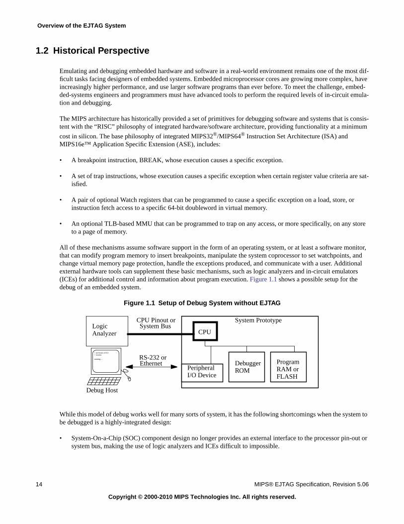
All of these mechanisms assume software support in the form of an operating system, or at least a software monitor,that can modify program memory to insert breakpoints, manipulate the system coprocessor to set watchpoints, andchange virtual memory page protection, handle the exceptions produced, and communicate with a user. Additionalexternal hardware tools can supplement these basic mechanisms, such as logic analyzers and in-circuit emulators(ICEs) for additional control and information about program execution. Figure 1.1 shows a possible setup for thedebug of an embedded system.
Figure 1.1 Setup of Debug System without EJTAG
While this model of debug works well for many sorts of system, it has the following shortcomings when the system tobe debugged is a highly-integrated design:
• System-On-a-Chip (SOC) component design no longer provides an external interface to the processor pin-out orsystem bus, making the use of logic analyzers and ICEs difficult to impossible.
Debug Host
LogicAnalyzer CPU
PeripheralI/O Device
DebuggerROM
ProgramRAM orFLASH
System PrototypeCPU Pinout orSystem Bus
RS-232 orEthernet
> set break at 0x3> resume
running....
1.2 Historical Perspective
MIPS® EJTAG Specification, Revision 5.06 15
Copyright © 2000-2010 MIPS Technologies Inc. All rights reserved.
• Debugging based on software breakpoints or the insertion of trap-on-condition instructions assumes that pro-grams reside in RAM. It is impractical for fully ROM-based systems and assumes support in the O/S for thesetechniques.
• For consumer electronic applications, a communication port like Ethernet or RS-232 serves no purpose beyondsoftware debug and adds disproportionately to the cost and size of the design.
• Similarly, the ROM necessary to support a debug software monitor on a consumer electronic application couldadd unacceptable costs.
One alternative to ICE is a specially-packaged device that is a bond-out of the chip. But this solution has the disad-vantage of adding to overall product development cost. It also adds the extra requirement of a specially-designedPCB that is needed to access the signals available only on the development chip.
On-Chip Debug (OCD) provides a solution for all these issues, and the EJTAG Debug Solution defines an advancedand scalable feature-set for OCD that allows debugging while executing CPU code at full speed.
One could say that OCD puts the ICE functionality on the chip. Although OCD does add a little extra die area for fea-tures that are only required during development, the die area is minimal. More importantly, with development timeand overall time-to-market becoming increasingly critical, the trade-off between die area and time seems reasonable.
Having the debug solution on-chip also makes it possible to use it for software upgrades, field testing, and for diag-nostics in the final product.
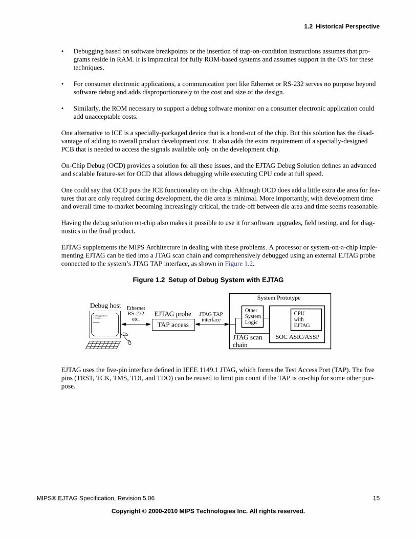
EJTAG supplements the MIPS Architecture in dealing with these problems. A processor or system-on-a-chip imple-menting EJTAG can be tied into a JTAG scan chain and comprehensively debugged using an external EJTAG probeconnected to the system’s JTAG TAP interface, as shown in Figure 1.2.
Figure 1.2 Setup of Debug System with EJTAG
EJTAG uses the five-pin interface defined in IEEE 1149.1 JTAG, which forms the Test Access Port (TAP). The fivepins (TRST, TCK, TMS, TDI, and TDO) can be reused to limit pin count if the TAP is on-chip for some other pur-pose.
> set break at 0x3> resume
running....
TAP access
Debug hostEJTAG probe
EthernetRS-232
etc.JTAG TAPinterface
CPUwithEJTAG
SOC ASIC/ASSP
OtherSystemLogic
System Prototype
JTAG scanchain
Overview of the EJTAG System
16 MIPS® EJTAG Specification, Revision 5.06
Copyright © 2000-2010 MIPS Technologies Inc. All rights reserved.
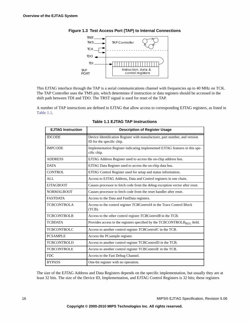
Figure 1.3 Test Access Port (TAP) to Internal Connections
This EJTAG interface through the TAP is a serial communications channel with frequencies up to 40 MHz on TCK.The TAP Controller uses the TMS pin, which determines if instruction or data registers should be accessed in theshift path between TDI and TDO. The TRST signal is used for reset of the TAP.
A number of TAP instructions are defined in EJTAG that allow access to corresponding EJTAG registers, as listed inTable 1.1.
The size of the EJTAG Address and Data Registers depends on the specific implementation, but usually they are atleast 32 bits. The size of the Device ID, Implementation, and EJTAG Control Registers is 32 bits; these registers
Table 1.1 EJTAG TAP Instructions
EJTAG Instruction Description of Register Usage
IDCODE Device Identification Register with manufacturer, part number, and versionID for the specific chip.
IMPCODE Implementation Register indicating implemented EJTAG features in this spe-cific chip.
ADDRESS EJTAG Address Register used to access the on-chip address bus.
DATA EJTAG Data Register used to access the on-chip data bus.
CONTROL EJTAG Control Register used for setup and status information.
ALL Access to EJTAG Address, Data and Control registers in one chain.
EJTAGBOOT Causes processor to fetch code from the debug exception vector after reset.
NORMALBOOT Causes processor to fetch code from the reset handler after reset.
FASTDATA Access to the Data and FastData registers.
TCBCONTROLA Access to the control register TCBControlA in the Trace Control Block(TCB).
TCBCONTROLB Access to the other control register TCBControlB in the TCB.
TCBDATA Provides access to the registers specified by the TCBCONTROLBREG field.
TCBCONTROLC Access to another control register TCBControlC in the TCB.
PCSAMPLE Access the PCsample register.
TCBCONTROLD Access to another control register TCBControlD in the TCB.
TCBCONTROLE Access to another control register TCBControlE in the TCB.
FDC Access to the Fast Debug Channel.
BYPASS One-bit register with no operation.
TAP Controller
Instruction, data &control registers
TRSTTMS
TCK
TDO
TDI
TAPPORT
1.3 EJTAG Capabilities
MIPS® EJTAG Specification, Revision 5.06 17
Copyright © 2000-2010 MIPS Technologies Inc. All rights reserved.
allow the user to do debug setup and provide important status information during the debug session. For exactdescriptions and size of these registers see 4.4 “Instruction Register and Special Instructions” on page 85.
1.3 EJTAG Capabilities
1.3.1 Debug Exception and Debug Mode
To allow inspection of the CPU state at any time in the execution flow, a debug exception with priority over all otherexceptions is introduced.
When a debug exception occurs, the CPU goes into Debug Mode, a special mode with no restrictions on access tocoprocessors, memory areas, etc., and where usual exceptions like address error and interrupt are masked.
The debug exception handler is executed in Debug Mode and provided by the debug system. It can be executed fromthe probe through a processor access, or may also reside in the application code if the developer chooses to use adebug task in the application.
An overall requirement is that debugging be non-intrusive to the application so execution of the application can becontinued after the needed debug operations. However, loss of real-time operation is inevitable when the debugexception handler is executed. The system designer may chose to indicate debug mode by a signal to certain hardwaremodules to freeze them when executing the debug exception handler.
EJTAG provides a standard debug I/O interface, enabling the use of traditional MIPS debug facilities on sys-tem-on-a-chip components. In addition, EJTAG provides the following new capabilities for software and systemdebug.
1.3.2 Off-board EJTAG Memory
EJTAG allows a MIPS processor in Debug Mode to reference instructions or data that are not resident on the systemunder test. This EJTAG memory is mapped to the processor as if it were virtual memory in the kseg3 segment, andreferences to it are converted into transactions on the TAP interface. Both instructions and data can be accessed inEJTAG memory, which allows debugging of systems without requiring the presence of a ROM monitor or debuggerscratchpad RAM. It also provides a communications channel between debug software executing on the processor andan external debugging agent.
The EJTAG probe polls the EJTAG Control Register through the TAP, and a bit in this register indicates when a pro-cessor access is pending. The physical address of the transaction is then available in the EJTAG Address Register,and the transaction size and read/write indication are available in the EJTAG Control Register. The EJTAG DataRegister is then accessed either to get data from a write or to provide data for a read. Finally the EJTAG Control Reg-ister is updated to indicate that the processor access is done.
Going through this sequence requires approximately 200 TCK periods for access to 32-bit address and data registers.With a 40 MHz TCK, the access time is in the range of 5 µs, resulting in a bandwidth in the range of 800 KB/s forinstruction and data transfers. However, the servicing may be optimized for instruction stuffing, because the addressdepends on the provided instructions and could thus be predicted to some extent. In addition, the FASTDATA feature(see Section 4.4.3 “FASTDATA Instruction”) of the TAP controller permits fast download or upload of data betweentarget memory and debug memory.
Overview of the EJTAG System
18 MIPS® EJTAG Specification, Revision 5.06
Copyright © 2000-2010 MIPS Technologies Inc. All rights reserved.
1.3.3 Debug Breakpoint Instruction
EJTAG introduces a new breakpoint instruction, SDBBP, which differs from the MIPS32 and MIPS64 BREAKinstruction in that the resulting exception, like the single-step and hardware breakpoint debug exceptions describedbelow, places the processor in Debug Mode and can fetch its associated handler code from EJTAG memory.
1.3.4 Hardware Breakpoints
EJTAG defines various types of hardware breakpoints for interrupting the CPU at certain transactions on the CPUbuses. The debug exception happens before the bus transaction causing the exception alters any memory or CPUstate, e.g., a fetched instruction with a break is not executed, or a data load/store transaction is not allowed to changethe register file or the memory.
Hardware breaks on instructions have the advantage over software debug breaks in that it is possible to set them inany address area. Furthermore, if memory cannot be altered by inserting SDBBP codes, the hardware breaks can stillbe used. Hardware data breakpoints allow breaks on load/store operations.
EJTAG implements two kinds of simple breaks:
• Instruction breaks, in which a break may be set on an instruction fetch from a specific virtual address
• Data breaks, in which a break may be set on a load/store reference from a specific virtual address, which addi-tionally can be qualified by a data value.
There may be up to 15 break channels of each type implemented, and each break channel may be programmed withaddress, address mask, ASID, and reference type.
EJTAG specification 4.00 and above also define complex breakpoints. There are many different types of complexbreakpoints defined the complex break chapter. Like the simple breaks, the complex breaks can cause a trigger signalthat can be used to enable or disable tracing via the MIPS PDtrace architecture.
1.3.5 Single-Step Execution
EJTAG provides support for single-step execution of programs and operating systems, without requiring that thecode reside in RAM.
1.4 EJTAG Components and Options
EJTAG hardware support consists of several distinct components: extensions to the MIPS processor core, the EJTAGTest Access Port, the Debug Control Register, and the Hardware Breakpoint Unit. Figure 1.4 shows the relationshipbetween these components in an EJTAG implementation. Some components and features are optional, and are imple-mented based on the needs of an implementation.
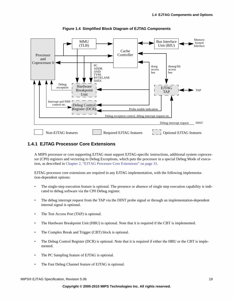
1.4 EJTAG Components and Options
MIPS® EJTAG Specification, Revision 5.06 19
Copyright © 2000-2010 MIPS Technologies Inc. All rights reserved.
Figure 1.4 Simplified Block Diagram of EJTAG Components
1.4.1 EJTAG Processor Core Extensions
A MIPS processor or core supporting EJTAG must support EJTAG-specific instructions, additional system coproces-sor (CP0) registers and vectoring to Debug Exceptions, which puts the processor in a special Debug Mode of execu-tion, as described in Chapter 2, “EJTAG Processor Core Extensions” on page 31.
EJTAG processor core extensions are required in any EJTAG implementation, with the following implementa-tion-dependent options:
• The single-step execution feature is optional. The presence or absence of single step execution capability is indi-cated to debug software via the CP0 Debug register.
• The debug interrupt request from the TAP via the DINT probe signal or through an implementation-dependentinternal signal is optional.
• The Test Access Port (TAP) is optional.
• The Hardware Breakpoint Unit (HBU) is optional. Note that it is required if the CBT is implemented.
• The Complex Break and Trigger (CBT) block is optional.
• The Debug Control Register (DCR) is optional. Note that it is required if either the HBU or the CBT is imple-mented.
• The PC Sampling feature of EJTAG is optional.
• The Fast Debug Channel feature of EJTAG is optional.
Processor
MMU
CacheController
HardwareBreakpoint
(TLB)Bus Interface
Debug ControlInterrupt and NMI
PCADDR
Debugexception
control etc.
ASIDTYPEBYTELANEDATA
EJTAGTAP TAP
Memory
DINT
SystemInterface
dmseg/fdc
Probe enable indication
Debug exception control, debug interrupt request etc.
Debug interrupt request
Unit (BIU)
andCoprocessor 0
Register (DCR)
Non-EJTAG features Required EJTAG features Optional EJTAG features
Unit
accessbus
drsegaccessbus
Overview of the EJTAG System
20 MIPS® EJTAG Specification, Revision 5.06
Copyright © 2000-2010 MIPS Technologies Inc. All rights reserved.
1.4.2 EJTAG Test Access Port
The EJTAG Test Access Port (TAP) provides a standard TAP interface to the EJTAG system. It is necessary for allTAP-based EJTAG capabilities for host-based debugging and processor access to external debug memory.
The TAP is optional. Implementation without a TAP implicitly disallows the EJTAG memory and TAP systemaccess capabilities, but provides the remaining EJTAG services (Debug Mode, single-step, software and hardwarebreakpoints) while executing from RAM or ROM. Refer to Chapter 4, “EJTAG Test Access Port” on page 81 formore information on the TAP.
Implementation without a TAP also disallows the PC Sampling feature.
The presence or absence of off-board EJTAG memory is indicated to debug software via the Debug Control Register.
1.4.3 Debug Control Register
The Debug Control Register (DCR) is a memory-mapped register that can be implemented as part of either the pro-cessor core or an external logic block. It indicates the availability and status of EJTAG features. The memory-mappedregion containing the DCR is available to software only in Debug Mode.
Implementation of the DCR is optional, but the DCR must be implemented if either the EJTAG TAP or EJTAG hard-ware breakpoints are implemented. The presence or absence of the DCR is indicated in the CP0 Debug register. Referto Chapter 3, “Debug Control Register” on page 75 for more information on the DCR.
1.4.4 Hardware Breakpoint Unit
The Hardware Breakpoint Unit implements memory-mapped registers that control the instruction and data hardwarebreakpoints. The memory-mapped region containing the hardware breakpoint registers is accessible to software onlyin Debug Mode.
EJTAG hardware breakpoint support, as described in Chapter 5, “Hardware Breakpoints” on page 111, is optional,and can be implemented with the following functionality:
• From zero to 15 independent instruction hardware breakpoints
• From zero to 15 independent data hardware breakpoints
• Breakpoint address comparisons for instruction and data hardware breakpoints optionally qualified with a com-parison of the MMU ASID
• Data hardware breakpoints optionally qualified with a data value comparison
• The sense of the data value qualifier can be inverted, that is, when the store data for example does NOT matchthe specified value in the data break register. This is an optional functionality whose presence is indicated by abit (15) in the DCR register. This feature is defined in revision 4.00 and above.
• Debug logic can optionally save the load data value in a specified drseg address register for software replay ofthe exception-causing load instruction. This is needed to preserve the load data value in situations where the datawas obtained not from non-volatile memory but from say a FIFO or an I/O register. Whether or not this feature isimplemented is indicated by a bit (14) in the DCR register. This feature is defined in revision 4.00 and above.
The presence or absence of hardware breakpoint capability is indicated to debug software in the DCR.
1.5 Complex Breakpoint and Trigger (CBT) Block
MIPS® EJTAG Specification, Revision 5.06 21
Copyright © 2000-2010 MIPS Technologies Inc. All rights reserved.
The number of breakpoints and the availability of optional qualifiers is indicated to debug software in the instructionand data breakpoint status registers.
1.4.5 Fast Debug Channel
EJTAG version 5.0 adds the optional Fast Debug Channel (FDC) mechanism for data transfer between a debughost/probe and a target. The FDC mechanism allows the user to set up a data transfer, and then resume normal opera-tion. The data transfer occurs in the background, and the target CPU can either choose to check the status of the trans-fer periodically, or it can choose to be interrupted at the end of the transfer.
The FDC mechanism adds two First In First Out (FIFO) structures that are mapped into the target CPU physicaladdress map. The probe uses the new FDC TAP instruction to access these FIFOs, while the CPU itself accesses themusing memory accesses.
When compared with the pre-existing FASTDATA mechanism (See Section 4.4.3 “FASTDATA Instruction”), theprimary advantage of FDC is that it does not require the CPU to be blocked when the probe is reading or writing tothe data transfer FIFOs. This significantly reduces the CPU overhead and makes data transfers far less intrusive to thecode executing on the CPU.
More information can be found in Chapter 8, “Fast Debug Channel” on page 165.
1.5 Complex Breakpoint and Trigger (CBT) Block
The presence or absence of this optional block is indicated by a bit (10) in the DCR register. Each of the listed fea-tures of this block is optional and the presence or absence of this feature is indicated by bits in the CBTcontrol regis-ter which is a drseg address-mapped register at address 0x8000:
• Pass Counters - each break channel, instruction, data, or complex has a counter associated with it that enables abreakpoint to be taken only after the address/value condition has been met a certain number of times.
• Ability to support 0 to 15 ‘tuples’ - breakpoints that only fire when both instruction and data conditions match ona single instruction.
• Qualified Instruction breakpoints - breakpoints that can be enabled and disabled based on the state of a databreakpoint condition, which can be used to only match on instructions executed in a certain process.
• Primed breakpoints - breakpoints that are only enabled when another breakpoint has occurred, which allowsbreaking on a simple sequences of events. It is an implementation choice as to how many priming conditions aresupported for each break; up to 16 priming conditions are possible. Note that the default priming condition is thesimple break, that is, no priming condition.
• Stopwatch timer - a counter that can be configured to start or stop based on specific instruction breakpoints. It isan implementation choice which breakpoints are used to start and stop the stopwatch timer. Upto two such pairsmay be supported.
1.6 EJTAG-Specific Coprocessor 0 Registers
This section summarizes the registers and special memory that are used for the EJTAG debug solution. More detailedinformation regarding mandatory and optional registers and memory locations is provided in the relevant chapter.
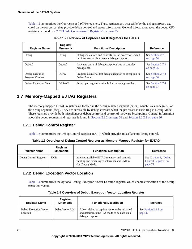
Overview of the EJTAG System
22 MIPS® EJTAG Specification, Revision 5.06
Copyright © 2000-2010 MIPS Technologies Inc. All rights reserved.
Table 1.2 summarizes the Coprocessor 0 (CP0) registers. These registers are accessible by the debug software exe-cuted on the processor; they provide debug control and status information. General information about the debug CP0registers is found in 2.7 “EJTAG Coprocessor 0 Registers” on page 55.
1.7 Memory-Mapped EJTAG Registers
The memory-mapped EJTAG registers are located in the debug register segment (drseg), which is a sub-segment ofthe debug segment (dseg). They are accessible by debug software when the processor is executing in Debug Mode.These registers provide both miscellaneous debug control and control of hardware breakpoints. General informationabout the debug segment and registers is found in Section 2.2.2 on page 32 and Section 2.2.2.2 on page 36.
1.7.1 Debug Control Register
Table 1.3 summarizes the Debug Control Register (DCR), which provides miscellaneous debug control.
1.7.2 Debug Exception Vector Location
Table 1.4 summarizes the optional Debug Exception Vector Location register, which enables relocation of the debugexception vector..
Table 1.2 Overview of Coprocessor 0 Registers for EJTAG
Register NameRegister
Mnemonic Functional Description Reference
Debug Debug Debug indications and controls for the processor, includ-ing information about recent debug exception.
See Section 2.7.1on page 56
Debug2 Debug2 Indicates cause of debug exceptions due to complexbreakpoints.
See Section 2.7.2on page 65
Debug ExceptionProgram Counter
DEPC Program counter at last debug exception or exception inDebug Mode.
See Section 2.7.3on page 66
Debug Exception Save DESAVE Scratchpad register available for the debug handler. See Section 2.7.4on page 67
Table 1.3 Overview of Debug Control Register as Memory-Mapped Register for EJTAG
Register NameRegister
Mnemonic Functional Description Reference
Debug Control Register DCR Indicates available EJTAG memory, and controlsenabling and disabling of interrupts and NMI inNon-Debug Mode.
See Chapter 3, “DebugControl Register” onpage 75
Table 1.4 Overview of Debug Exception Vector Location Register
Register NameRegister
Mnemonic Functional Description Reference
Debug Exception VectorLocation
DebugVectorAddr Allows debug exception vector to be relocatedand determines the ISA mode to be used on adebug exception.
See Section 2.3.2 onpage 42
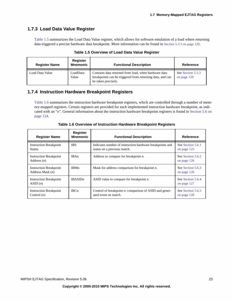
1.7 Memory-Mapped EJTAG Registers
MIPS® EJTAG Specification, Revision 5.06 23
Copyright © 2000-2010 MIPS Technologies Inc. All rights reserved.
1.7.3 Load Data Value Register
Table 1.5 summarizes the Load Data Value register, which allows for software emulation of a load where returningdata triggered a precise hardware data breakpoint. More information can be found in Section 5.3.3 on page 120.
1.7.4 Instruction Hardware Breakpoint Registers
Table 1.6 summarizes the instruction hardware breakpoint registers, which are controlled through a number of mem-ory-mapped registers. Certain registers are provided for each implemented instruction hardware breakpoint, as indi-cated with an “n”. General information about the instruction hardware breakpoint registers is found in Section 5.6 onpage 124.
Table 1.5 Overview of Load Data Value Register
Register NameRegister
Mnemonic Functional Description Reference
Load Data Value LoadData-Value
Contains data returned from load, when hardware databreakpoints can be triggered from returning data, and canbe taken precisely.
See Section 5.3.3on page 120
Table 1.6 Overview of Instruction Hardware Breakpoint Registers
Register NameRegister
Mnemonic Functional Description Reference
Instruction BreakpointStatus
IBS Indicates number of instruction hardware breakpoints andstatus on a previous match.
See Section 5.6.1on page 125
Instruction BreakpointAddress (n)
IBAn Address to compare for breakpoint n. See Section 5.6.2on page 126
Instruction BreakpointAddress Mask (n)
IBMn Mask for address comparison for breakpoint n. See Section 5.6.3on page 126
Instruction BreakpointASID (n)
IBASIDn ASID value to compare for breakpoint n. See Section 5.6.4on page 127
Instruction BreakpointControl (n)
IBCn Control of breakpoint n: comparison of ASID and gener-ated event on match.
See Section 5.6.5on page 128
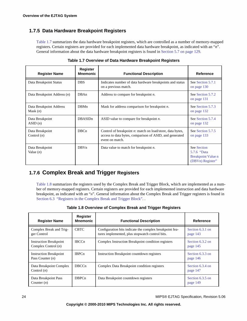
Overview of the EJTAG System
24 MIPS® EJTAG Specification, Revision 5.06
Copyright © 2000-2010 MIPS Technologies Inc. All rights reserved.
1.7.5 Data Hardware Breakpoint Registers
Table 1.7 summarizes the data hardware breakpoint registers, which are controlled as a number of memory-mappedregisters. Certain registers are provided for each implemented data hardware breakpoint, as indicated with an “n”.General information about the data hardware breakpoint registers is found in Section 5.7 on page 129.
1.7.6 Complex Break and Trigger Registers
Table 1.8 summarizes the registers used by the Complex Break and Trigger Block, which are implemented as a num-ber of memory-mapped registers. Certain registers are provided for each implemented instruction and data hardwarebreakpoint, as indicated with an “n”. General information about the Complex Break and Trigger registers is found inSection 6.3 “Registers in the Complex Break and Trigger Block”. .
Table 1.7 Overview of Data Hardware Breakpoint Registers
Register NameRegister
Mnemonic Functional Description Reference
Data Breakpoint Status DBS Indicates number of data hardware breakpoints and statuson a previous match.
See Section 5.7.1on page 130
Data Breakpoint Address (n) DBAn Address to compare for breakpoint n. See Section 5.7.2on page 131
Data Breakpoint AddressMask (n)
DBMn Mask for address comparison for breakpoint n. See Section 5.7.3on page 132
Data BreakpointASID (n)
DBASIDn ASID value to compare for breakpoint n. See Section 5.7.4on page 132
Data BreakpointControl (n)
DBCn Control of breakpoint n: match on load/store, data bytes,access to data bytes, comparison of ASID, and generatedevent on match.
See Section 5.7.5on page 133
Data BreakpointValue (n)
DBVn Data value to match for breakpoint n. See Section5.7.6 “DataBreakpoint Value n(DBVn) Register”
Table 1.8 Overview of Complex Break and Trigger Registers
Register NameRegister
Mnemonic Functional Description Reference
Complex Break and Trig-ger Control
CBTC Configuration bits indicate the complex breakpoint fea-tures implemented, plus stopwatch control bits.
Section 6.3.1 onpage 143
Instruction BreakpointComplex Control (n)
IBCCn Complex Instruction Breakpoint condition registers Section 6.3.2 onpage 145
Instruction BreakpointPass Counter (n)
IBPCn Instruction Breakpoint countdown registers Section 6.3.3 onpage 146
Data Breakpoint ComplexControl (n)
DBCCn Complex Data Breakpoint condition registers Section 6.3.4 onpage 147
Data Breakpoint PassCounter (n)
DBPCn Data Breakpoint countdown registers Section 6.3.5 onpage 149
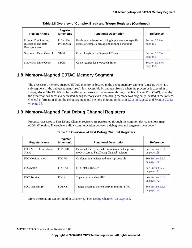
1.8 Memory-Mapped EJTAG Memory Segment
MIPS® EJTAG Specification, Revision 5.06 25
Copyright © 2000-2010 MIPS Technologies Inc. All rights reserved.
1.8 Memory-Mapped EJTAG Memory Segment
The processor’s memory-mapped EJTAG memory is located in the debug memory segment (dmseg), which is asub-segment of the debug segment (dseg). It is accessible by debug software when the processor is executing inDebug Mode. The EJTAG probe handles all accesses to this segment through the Test Access Port (TAP), wherebythe processor has access to dedicated debug memory even if no debug memory was originally located in the system.General information about the debug segment and memory is found in Section 2.2.2 on page 32 and Section 2.2.2.1on page 35.
1.9 Memory-Mapped Fast Debug Channel Registers
Processor accesses to Fast Debug Channel registers are performed through the common device memory map(CDMM) region. The registers allow communication between a debug host and target-resident code.f
More information can be found in Chapter 8, “Fast Debug Channel” on page 165.
Priming Condition A,Instruction and DataBreakpoint (n)
PrCndAIn,PrCndADn
Read-only registers describing implementation-specificdetails of complex breakpoint priming conditions
Section 6.3.6 onpage 150
Stopwatch Timer Control STCtl Control register for Stopwatch Timer Section 6.3.7 onpage 151
Stopwatch Timer Count STCnt Count register for Stopwatch Timer Section 6.3.8 onpage 153
Table 1.9 Overview of Fast Debug Channel Registers
Register NameRegister
Mnemonic Functional Description Reference
FDC Access Control andStatus
FDACSR Defines device type, and controls user and supervisormode access to Fast Debug Channel registers
See Section 8.3.1on page 169
FDC Configuration FDCFG Configuration register and interrupt controls See Section 8.3.2on page 170
FDC Status FDSTAT FIFO status register See Section 8.3.3on page 171
FDC Receive FDRX Top entry in receive FIFO See Section 8.3.4on page 172
FDC Transmit (n) FDTXn Tagged access to bottom entry in transmit FIFO See Section 8.3.5on page 172
Table 1.8 Overview of Complex Break and Trigger Registers (Continued)
Register NameRegister
Mnemonic Functional Description Reference
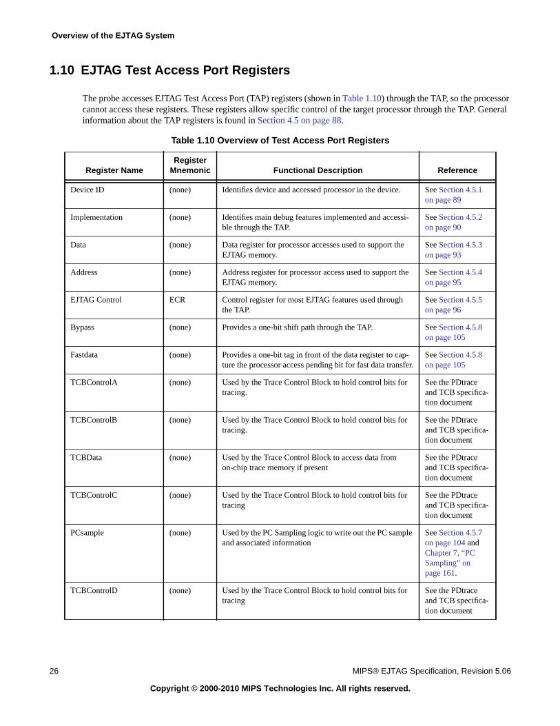
Overview of the EJTAG System
26 MIPS® EJTAG Specification, Revision 5.06
Copyright © 2000-2010 MIPS Technologies Inc. All rights reserved.
1.10 EJTAG Test Access Port Registers
The probe accesses EJTAG Test Access Port (TAP) registers (shown in Table 1.10) through the TAP, so the processorcannot access these registers. These registers allow specific control of the target processor through the TAP. Generalinformation about the TAP registers is found in Section 4.5 on page 88.
Table 1.10 Overview of Test Access Port Registers
Register NameRegister
Mnemonic Functional Description Reference
Device ID (none) Identifies device and accessed processor in the device. See Section 4.5.1on page 89
Implementation (none) Identifies main debug features implemented and accessi-ble through the TAP.
See Section 4.5.2on page 90
Data (none) Data register for processor accesses used to support theEJTAG memory.
See Section 4.5.3on page 93
Address (none) Address register for processor access used to support theEJTAG memory.
See Section 4.5.4on page 95
EJTAG Control ECR Control register for most EJTAG features used throughthe TAP.
See Section 4.5.5on page 96
Bypass (none) Provides a one-bit shift path through the TAP. See Section 4.5.8on page 105
Fastdata (none) Provides a one-bit tag in front of the data register to cap-ture the processor access pending bit for fast data transfer.
See Section 4.5.8on page 105
TCBControlA (none) Used by the Trace Control Block to hold control bits fortracing.
See the PDtraceand TCB specifica-tion document
TCBControlB (none) Used by the Trace Control Block to hold control bits fortracing.
See the PDtraceand TCB specifica-tion document
TCBData (none) Used by the Trace Control Block to access data fromon-chip trace memory if present
See the PDtraceand TCB specifica-tion document
TCBControlC (none) Used by the Trace Control Block to hold control bits fortracing
See the PDtraceand TCB specifica-tion document
PCsample (none) Used by the PC Sampling logic to write out the PC sampleand associated information
See Section 4.5.7on page 104 andChapter 7, “PCSampling” onpage 161.
TCBControlD (none) Used by the Trace Control Block to hold control bits fortracing
See the PDtraceand TCB specifica-tion document
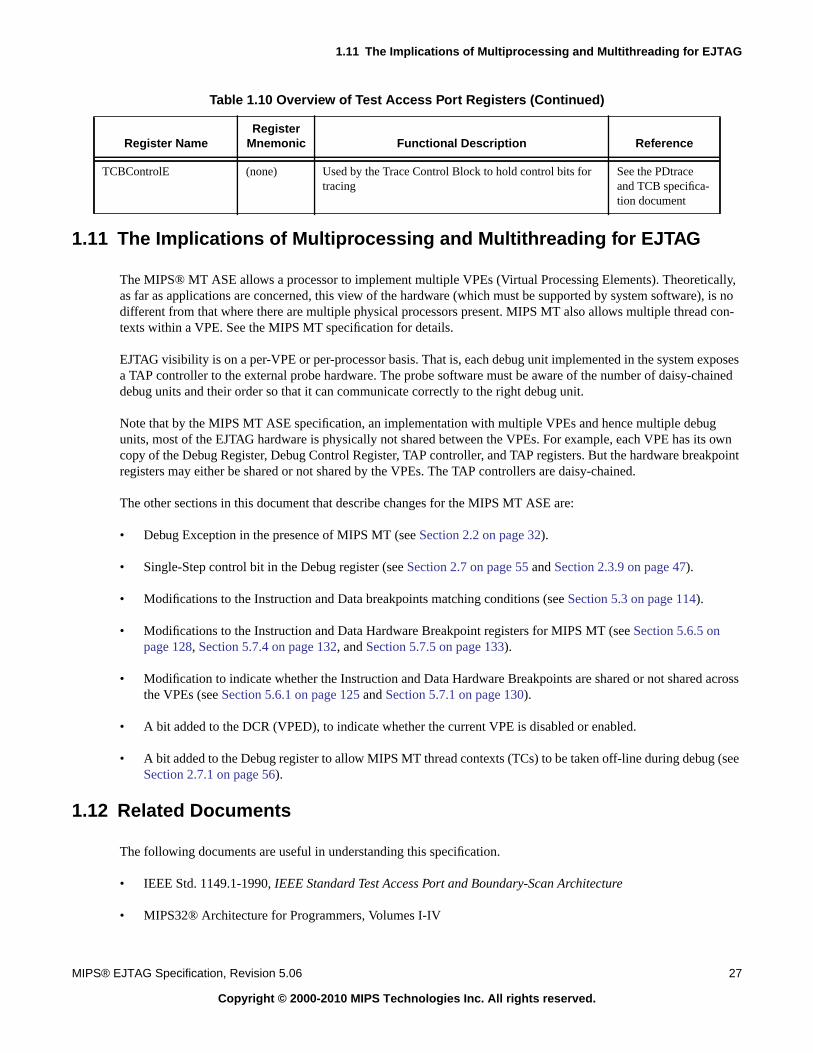
1.11 The Implications of Multiprocessing and Multithreading for EJTAG
MIPS® EJTAG Specification, Revision 5.06 27
Copyright © 2000-2010 MIPS Technologies Inc. All rights reserved.
1.11 The Implications of Multiprocessing and Multithreading for EJTAG
The MIPS® MT ASE allows a processor to implement multiple VPEs (Virtual Processing Elements). Theoretically,as far as applications are concerned, this view of the hardware (which must be supported by system software), is nodifferent from that where there are multiple physical processors present. MIPS MT also allows multiple thread con-texts within a VPE. See the MIPS MT specification for details.
EJTAG visibility is on a per-VPE or per-processor basis. That is, each debug unit implemented in the system exposesa TAP controller to the external probe hardware. The probe software must be aware of the number of daisy-chaineddebug units and their order so that it can communicate correctly to the right debug unit.
Note that by the MIPS MT ASE specification, an implementation with multiple VPEs and hence multiple debugunits, most of the EJTAG hardware is physically not shared between the VPEs. For example, each VPE has its owncopy of the Debug Register, Debug Control Register, TAP controller, and TAP registers. But the hardware breakpointregisters may either be shared or not shared by the VPEs. The TAP controllers are daisy-chained.
The other sections in this document that describe changes for the MIPS MT ASE are:
• Debug Exception in the presence of MIPS MT (see Section 2.2 on page 32).
• Single-Step control bit in the Debug register (see Section 2.7 on page 55 and Section 2.3.9 on page 47).
• Modifications to the Instruction and Data breakpoints matching conditions (see Section 5.3 on page 114).
• Modifications to the Instruction and Data Hardware Breakpoint registers for MIPS MT (see Section 5.6.5 onpage 128, Section 5.7.4 on page 132, and Section 5.7.5 on page 133).
• Modification to indicate whether the Instruction and Data Hardware Breakpoints are shared or not shared acrossthe VPEs (see Section 5.6.1 on page 125 and Section 5.7.1 on page 130).
• A bit added to the DCR (VPED), to indicate whether the current VPE is disabled or enabled.
• A bit added to the Debug register to allow MIPS MT thread contexts (TCs) to be taken off-line during debug (seeSection 2.7.1 on page 56).
1.12 Related Documents
The following documents are useful in understanding this specification.
• IEEE Std. 1149.1-1990, IEEE Standard Test Access Port and Boundary-Scan Architecture
• MIPS32® Architecture for Programmers, Volumes I-IV
TCBControlE (none) Used by the Trace Control Block to hold control bits fortracing
See the PDtraceand TCB specifica-tion document
Table 1.10 Overview of Test Access Port Registers (Continued)
Register NameRegister
Mnemonic Functional Description Reference
Overview of the EJTAG System
28 MIPS® EJTAG Specification, Revision 5.06
Copyright © 2000-2010 MIPS Technologies Inc. All rights reserved.
• MIPS64® Architecture for Programmers, Volumes I-IV
• The PDtrace™ Interface and Trace Control Block Specification (MD00439)
• MIPS32® Architecture for Programmers Volume IV-f: The MIPS® MT Application-Specific Extension to theMIPS32® Architecture (MD00378)
• The iFlowtrace™ Architecture Specification (MD00526)
1.13 Notations and Conventions
This section defines notations and conventions that are used throughout this document.
1.13.1 Compliance
Throughout this document, compliance levels are indicated for specific features. Features are defined as Required,Optional, or Recommended.
Features defined as required are required of all processors claiming compatibility with the EJTAG architecture.
Features defined as optional provide a standardization that might or might not be appropriate for a particular EJTAGimplementation. If such a feature is implemented, it must be implemented as described in this document for a proces-sor to claim compatibility with the EJTAG architecture.
In some cases, there are features within features that have different levels of compliance. For example, if there is anoptional field within a required register, the register must be implemented, but the field does not have to be imple-mented, depending on the needs of the implementation. Similarly, if there is a required field within an optional regis-ter, if the register is implemented, it must have the specified field.
Features defined as recommended should be implemented unless there is an overriding need not to do so.
1.13.2 UNPREDICTABLE and UNDEFINED Operations
These definitions of UNPREDICTABLE and UNDEFINED are similar to the descriptions in the MIPS32 andMIPS64 specifications. They are included here for those readers who are not familiar with these documents.
The terms UNPREDICTABLE and UNDEFINED describe the behavior of the processor in certain cases. UNDE-FINED behavior or operations can occur only as the result of executing instructions in a privileged mode (in KernelMode or Debug Mode, or with the CP0 usable bit set in the Status register). Unprivileged software can never causeUNDEFINED behavior or operations. Conversely, both privileged and unprivileged software can cause UNPRE-DICTABLE results or operations.
1.13.2.1 UNPREDICTABLE
UNPREDICTABLE results can vary from implementation to implementation, instruction to instruction, or as a func-tion of time in the same implementation or instruction. Software can never depend on results that are UNPREDICT-ABLE. An UNPREDICTABLE operation might or might not cause a result to be generated. If it does generate aresult, the result is UNPREDICTABLE. UNPREDICTABLE operations can cause arbitrary exceptions.
UNPREDICTABLE results or operations have several implementation restrictions:
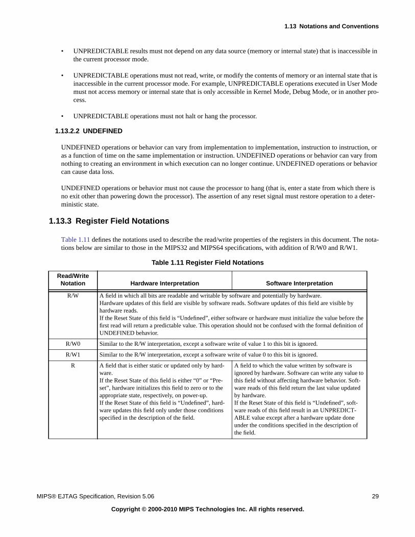
1.13 Notations and Conventions
MIPS® EJTAG Specification, Revision 5.06 29
Copyright © 2000-2010 MIPS Technologies Inc. All rights reserved.
• UNPREDICTABLE results must not depend on any data source (memory or internal state) that is inaccessible inthe current processor mode.
• UNPREDICTABLE operations must not read, write, or modify the contents of memory or an internal state that isinaccessible in the current processor mode. For example, UNPREDICTABLE operations executed in User Modemust not access memory or internal state that is only accessible in Kernel Mode, Debug Mode, or in another pro-cess.
• UNPREDICTABLE operations must not halt or hang the processor.
1.13.2.2 UNDEFINED
UNDEFINED operations or behavior can vary from implementation to implementation, instruction to instruction, oras a function of time on the same implementation or instruction. UNDEFINED operations or behavior can vary fromnothing to creating an environment in which execution can no longer continue. UNDEFINED operations or behaviorcan cause data loss.
UNDEFINED operations or behavior must not cause the processor to hang (that is, enter a state from which there isno exit other than powering down the processor). The assertion of any reset signal must restore operation to a deter-ministic state.
1.13.3 Register Field Notations
Table 1.11 defines the notations used to describe the read/write properties of the registers in this document. The nota-tions below are similar to those in the MIPS32 and MIPS64 specifications, with addition of R/W0 and R/W1.
Table 1.11 Register Field Notations
Read/WriteNotation Hardware Interpretation Software Interpretation
R/W A field in which all bits are readable and writable by software and potentially by hardware.Hardware updates of this field are visible by software reads. Software updates of this field are visible byhardware reads.If the Reset State of this field is “Undefined”, either software or hardware must initialize the value before thefirst read will return a predictable value. This operation should not be confused with the formal definition ofUNDEFINED behavior.
R/W0 Similar to the R/W interpretation, except a software write of value 1 to this bit is ignored.
R/W1 Similar to the R/W interpretation, except a software write of value 0 to this bit is ignored.
R A field that is either static or updated only by hard-ware.If the Reset State of this field is either “0” or “Pre-set”, hardware initializes this field to zero or to theappropriate state, respectively, on power-up.If the Reset State of this field is “Undefined”, hard-ware updates this field only under those conditionsspecified in the description of the field.
A field to which the value written by software isignored by hardware. Software can write any value tothis field without affecting hardware behavior. Soft-ware reads of this field return the last value updatedby hardware.If the Reset State of this field is “Undefined”, soft-ware reads of this field result in an UNPREDICT-ABLE value except after a hardware update doneunder the conditions specified in the description ofthe field.
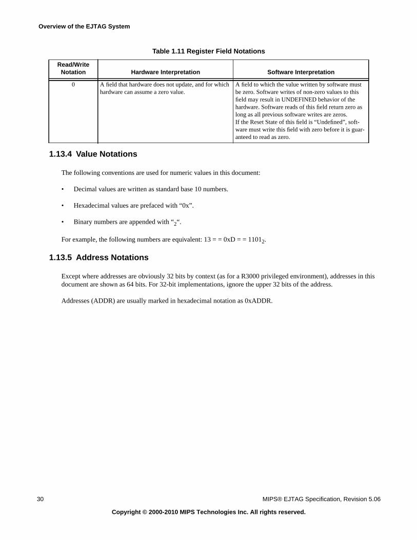
Overview of the EJTAG System
30 MIPS® EJTAG Specification, Revision 5.06
Copyright © 2000-2010 MIPS Technologies Inc. All rights reserved.
1.13.4 Value Notations
The following conventions are used for numeric values in this document:
• Decimal values are written as standard base 10 numbers.
• Hexadecimal values are prefaced with “0x”.
• Binary numbers are appended with “2“.
For example, the following numbers are equivalent: 13 = = 0xD = = 11012.
1.13.5 Address Notations
Except where addresses are obviously 32 bits by context (as for a R3000 privileged environment), addresses in thisdocument are shown as 64 bits. For 32-bit implementations, ignore the upper 32 bits of the address.
Addresses (ADDR) are usually marked in hexadecimal notation as 0xADDR.
0 A field that hardware does not update, and for whichhardware can assume a zero value.
A field to which the value written by software mustbe zero. Software writes of non-zero values to thisfield may result in UNDEFINED behavior of thehardware. Software reads of this field return zero aslong as all previous software writes are zeros.If the Reset State of this field is “Undefined”, soft-ware must write this field with zero before it is guar-anteed to read as zero.
Table 1.11 Register Field Notations
Read/WriteNotation Hardware Interpretation Software Interpretation
Chapter 2
MIPS® EJTAG Specification, Revision 5.06 31
Copyright © 2000-2010 MIPS Technologies Inc. All rights reserved.
EJTAG Processor Core Extensions
This chapter describes the behavior of processors that support EJTAG. It contains the following sections:
• Section 2.1 “Overview”
• Section 2.2 “Debug Mode Execution”
• Section 2.3 “Debug Exceptions”
• Section 2.4 “Debug Mode Exceptions”
• Section 2.5 “Interrupts and NMIs”
• Section 2.6 “Reset and Soft Reset of Processor”
• Section 2.8 “EJTAG Instructions”
• Section 2.7 “EJTAG Coprocessor 0 Registers”
2.1 Overview
The extensions for EJTAG provide the following major features:
• Debug Mode, associated exceptions and dedicated debug vector
• Instruction set extensions: SDBBP (Software Debug Breakpoint) and DERET (Debug Exception Return)
• CP0 registers: Debug, DEPC and DESAVE
• Memory-mapped debug segment (dseg) (optional)
• Interrupt and NMI control from Debug Control Register (DCR) (optional)
• Single step (optional)
• Debug interrupt request signal (optional)
Note that some of the features are optional.
The general description in this chapter covers MIPS32 and MIPS64 processors, implying an R4000-like privilegedenvironment. Differences for processors with R3000 privileged environments are described in Appendix A,“Differences for R3000 Privileged Environments” on page 187.
EJTAG Processor Core Extensions
32 MIPS® EJTAG Specification, Revision 5.06
Copyright © 2000-2010 MIPS Technologies Inc. All rights reserved.
2.2 Debug Mode Execution
Debug Mode is entered only through a debug exception. It is exited as a result of either the execution of a DERETinstruction or application of a reset or soft reset.
When the processor is operating in Debug Mode, it has access to the same resources, instructions, and CP0 registersas it has in Kernel Mode. The restrictions on Kernel Mode accesses (non-zero coprocessor references, access toextended addressing controlled by UX, SX, KX, etc.) apply equally to Debug Mode, but Debug Mode provides someadditional capabilities described in this chapter.
Other processor modes (Kernel Mode, Supervisor Mode, User Mode) are collectively considered as Non-DebugMode. Debug software can determine if the processor is in Non-Debug Mode or Debug Mode through the DM bit inthe Debug register.
A debug exception in a processor implementing the MIPS MT ASE will cause all other TCs (Thread Contexts) in theprocessor, except the one executing the exception handler, to be suspended from concurrent execution until theDERET instruction is executed. Debug-mode execution takes priority over all other TC scheduling rules in MIPSMT. A TC which is otherwise not permitted to issue instructions, due to a Halted, non-Activated (see the MIPS MTspecification), or OffLine state (see Section 2.7.1 on page 56) may still be used to service a debug exception.
When a MIPS MT processor is operating in Debug Mode, it has access to the same resources and capabilities as if theVPE in Debug Mode had the MVP bit of the VPEConf0 register set, which allows access to all the processor’s VPEs.
The ability of an OffLine MIPS MT TC to execute in Debug mode makes it possible for EJTAG-based debuggers toallow other TCs and/or other VPEs to continue executing while a particular TC has been stopped for debugging. TheDebug exception handler can cause the TC to put itself, and/or other TCs, in an OffLine state and then execute aDERET. On exiting Debug mode, the processor will resume normal scheduling of “on-line” TCs, but the OffLineones will remain frozen until released by, for example, service of a subsequent DINT Debug exception.
It is not a requirement in EJTAG, but it is left as an implementation option in multiprocessor/multicore systemswhether or not a global debug state is defined and can be set by the debugger to suspend other processors when one ofthe processors in a multi-core system encounters debug exception. Similarly, implementation can also trigger re-start-ing of other processors when the one in debug mode executes a DERET. See Appendix <TBD> for a description ofthis mechanism.
2.2.1 Debug Mode Instruction Set
The full native ISA of the processor is accessible in Debug Mode.
Coprocessor loads and stores to the dseg segment are not supported. The operation of the processor is UNDEFINEDif a coprocessor load or store to dseg is executed in Debug Mode. Refer to Section 2.2.2 on page 32 for more informa-tion on the dseg address space.
2.2.2 Debug Mode Address Space
Debug Mode access to unmapped address space is identical to that of Kernel Mode. Mapped addresses are accessibleas in Kernel Mode, but only if a valid translation is immediately provided by the MMU. This is because a memoryaccess that would cause a TLB-type exception in Kernel Mode, would, when tried in Debug Mode, cause re-entryinto Debug Mode through an exception (see Section 2.4 on page 50). Memory accesses usually causing TLB-typeexceptions are therefore not handled by the usual memory management routines if these memory accesses are madewhile in Debug Mode.
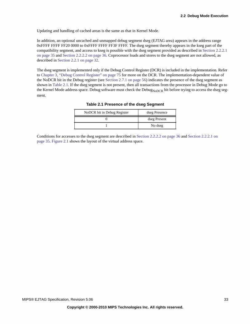
2.2 Debug Mode Execution
MIPS® EJTAG Specification, Revision 5.06 33
Copyright © 2000-2010 MIPS Technologies Inc. All rights reserved.
Updating and handling of cached areas is the same as that in Kernel Mode.
In addition, an optional uncached and unmapped debug segment dseg (EJTAG area) appears in the address range0xFFFF FFFF FF20 0000 to 0xFFFF FFFF FF3F FFFF. The dseg segment thereby appears in the kseg part of thecompatibility segment, and access to kseg is possible with the dseg segment provided as described in Section 2.2.2.1on page 35 and Section 2.2.2.2 on page 36. Coprocessor loads and stores to the dseg segment are not allowed, asdescribed in Section 2.2.1 on page 32.
The dseg segment is implemented only if the Debug Control Register (DCR) is included in the implementation. Referto Chapter 3, “Debug Control Register” on page 75 for more on the DCR. The implementation-dependent value ofthe NoDCR bit in the Debug register (see Section 2.7.1 on page 56) indicates the presence of the dseg segment asshown in Table 2.1. If the dseg segment is not present, then all transactions from the processor in Debug Mode go tothe Kernel Mode address space. Debug software must check the DebugNoDCR bit before trying to access the dseg seg-ment.
Conditions for accesses to the dseg segment are described in Section 2.2.2.2 on page 36 and Section 2.2.2.1 onpage 35. Figure 2.1 shows the layout of the virtual address space.
Table 2.1 Presence of the dseg Segment
NoDCR bit in Debug Register dseg Presence
0 dseg Present
1 No dseg
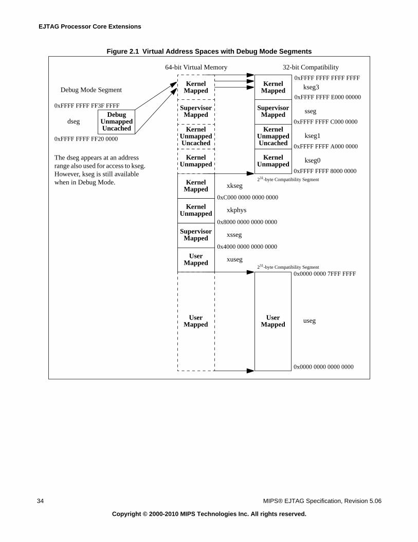
EJTAG Processor Core Extensions
34 MIPS® EJTAG Specification, Revision 5.06
Copyright © 2000-2010 MIPS Technologies Inc. All rights reserved.
Figure 2.1 Virtual Address Spaces with Debug Mode Segments
0x4000 0000 0000 0000
0x8000 0000 0000 0000
64-bit Virtual Memory 32-bit Compatibility
0xFFFF FFFF FFFF FFFF
0xFFFF FFFF E000 00000
0xFFFF FFFF C000 0000
0xFFFF FFFF A000 0000
0xFFFF FFFF 8000 0000
0x0000 0000 7FFF FFFF
0x0000 0000 0000 0000
0xC000 0000 0000 0000
xkseg
xkphys
xsseg
xuseg
useg
kseg0
kseg1
sseg
kseg3
KernelUnmapped
KernelMapped
SupervisorMapped
KernelUnmappedUncached
UserMapped
KernelMapped
SupervisorMapped
KernelUnmapped
UserMapped
231-byte Compatibility Segment
231-byte Compatibility Segment
UserMapped
KernelUnmapped
KernelMapped
SupervisorMapped
KernelUnmappedUncached
DebugUnmappedUncached
0xFFFF FFFF FF3F FFFF
dseg
0xFFFF FFFF FF20 0000
Debug Mode Segment
The dseg appears at an addressrange also used for access to kseg.However, kseg is still availablewhen in Debug Mode.
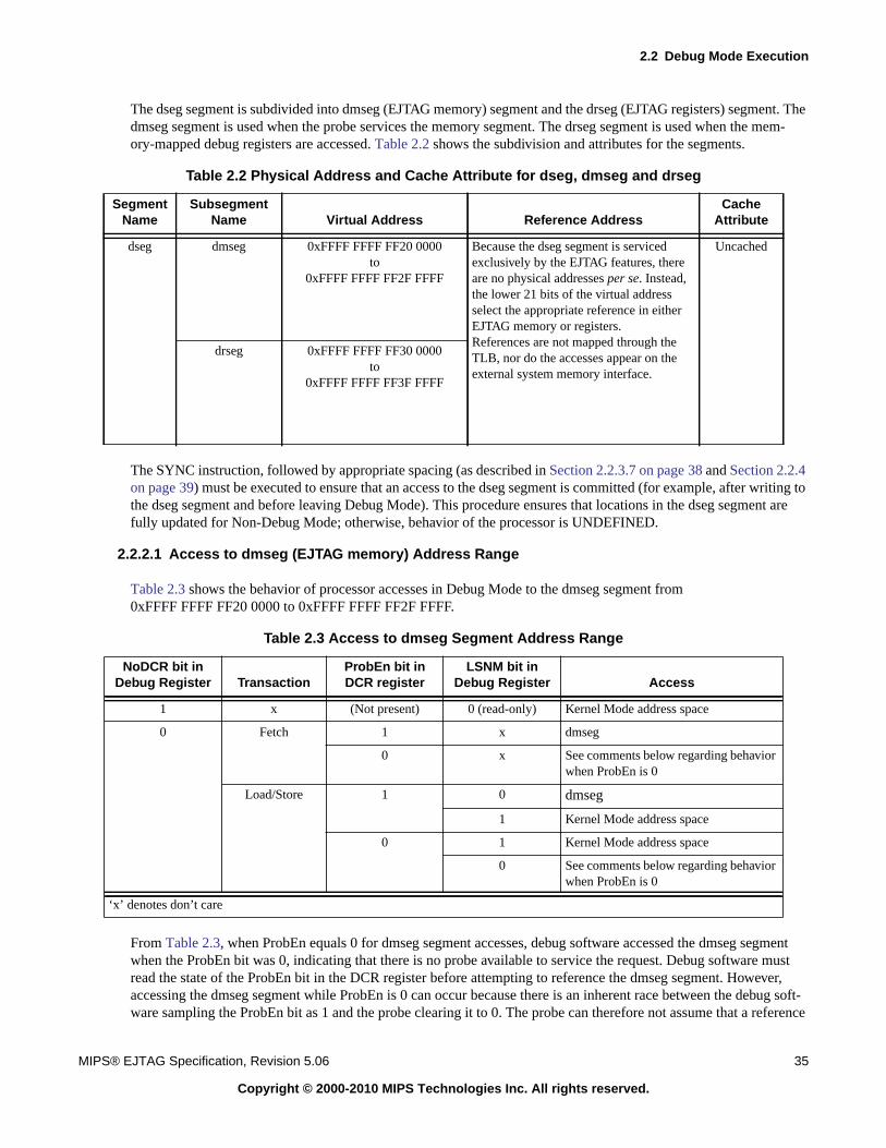
2.2 Debug Mode Execution
MIPS® EJTAG Specification, Revision 5.06 35
Copyright © 2000-2010 MIPS Technologies Inc. All rights reserved.
The dseg segment is subdivided into dmseg (EJTAG memory) segment and the drseg (EJTAG registers) segment. Thedmseg segment is used when the probe services the memory segment. The drseg segment is used when the mem-ory-mapped debug registers are accessed. Table 2.2 shows the subdivision and attributes for the segments.
The SYNC instruction, followed by appropriate spacing (as described in Section 2.2.3.7 on page 38 and Section 2.2.4on page 39) must be executed to ensure that an access to the dseg segment is committed (for example, after writing tothe dseg segment and before leaving Debug Mode). This procedure ensures that locations in the dseg segment arefully updated for Non-Debug Mode; otherwise, behavior of the processor is UNDEFINED.
2.2.2.1 Access to dmseg (EJTAG memory) Address Range
Table 2.3 shows the behavior of processor accesses in Debug Mode to the dmseg segment from0xFFFF FFFF FF20 0000 to 0xFFFF FFFF FF2F FFFF.
From Table 2.3, when ProbEn equals 0 for dmseg segment accesses, debug software accessed the dmseg segmentwhen the ProbEn bit was 0, indicating that there is no probe available to service the request. Debug software mustread the state of the ProbEn bit in the DCR register before attempting to reference the dmseg segment. However,accessing the dmseg segment while ProbEn is 0 can occur because there is an inherent race between the debug soft-ware sampling the ProbEn bit as 1 and the probe clearing it to 0. The probe can therefore not assume that a reference
Table 2.2 Physical Address and Cache Attribute for dseg, dmseg and drseg
SegmentName
SubsegmentName Virtual Address Reference Address
CacheAttribute
dseg dmseg 0xFFFF FFFF FF20 0000to
0xFFFF FFFF FF2F FFFF
Because the dseg segment is servicedexclusively by the EJTAG features, thereare no physical addresses per se. Instead,the lower 21 bits of the virtual addressselect the appropriate reference in eitherEJTAG memory or registers.References are not mapped through theTLB, nor do the accesses appear on theexternal system memory interface.
Uncached
drseg 0xFFFF FFFF FF30 0000to
0xFFFF FFFF FF3F FFFF
Table 2.3 Access to dmseg Segment Address Range
NoDCR bit inDebug Register Transaction
ProbEn bit inDCR register
LSNM bit inDebug Register Access
1 x (Not present) 0 (read-only) Kernel Mode address space
0 Fetch 1 x dmseg
0 x See comments below regarding behaviorwhen ProbEn is 0
Load/Store 1 0 dmseg
1 Kernel Mode address space
0 1 Kernel Mode address space
0 See comments below regarding behaviorwhen ProbEn is 0
‘x’ denotes don’t care
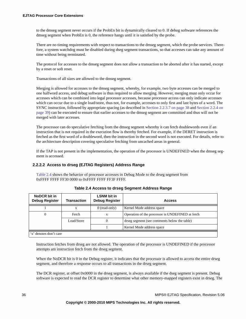
EJTAG Processor Core Extensions
36 MIPS® EJTAG Specification, Revision 5.06
Copyright © 2000-2010 MIPS Technologies Inc. All rights reserved.
to the dmseg segment never occurs if the ProbEn bit is dynamically cleared to 0. If debug software references thedmseg segment when ProbEn is 0, the reference hangs until it is satisfied by the probe.
There are no timing requirements with respect to transactions to the dmseg segment, which the probe services. There-fore, a system watchdog must be disabled during dseg segment transactions, so that accesses can take any amount oftime without being terminated.
The protocol for accesses to the dmseg segment does not allow a transaction to be aborted after it has started, exceptby a reset or soft reset.
Transactions of all sizes are allowed to the dmseg segment.
Merging is allowed for accesses to the dmseg segment, whereby, for example, two byte accesses can be merged toone halfword access, and debug software is thus required to allow merging. However, merging must only occur foraccesses which can be combined into legal processor accesses, because processor access can only indicate accesseswhich can occur due to a single load/store, thus not, for example, accesses to only first and last bytes of a word. TheSYNC instruction, followed by appropriate spacing (as described in Section 2.2.3.7 on page 38 and Section 2.2.4 onpage 39) can be executed to ensure that earlier accesses to the dmseg segment are committed and thus will not bemerged with later accesses.
The processor can do speculative fetching from the dmseg segment whereby it can fetch doublewords even if aninstruction that is not required in the execution flow is thereby fetched. For example, if the DERET instruction isfetched as the first word of a doubleword, then the instruction in the second word is not executed. For details, refer tothe architecture description covering speculative fetching from uncached areas in general.
If the TAP is not present in the implementation, the operation of the processor is UNDEFINED when the dmseg seg-ment is accessed.
2.2.2.2 Access to drseg (EJTAG Registers) Address Range
Table 2.4 shows the behavior of processor accesses in Debug Mode to the drseg segment from0xFFFF FFFF FF30 0000 to 0xFFFF FFFF FF3F FFFF.
Instruction fetches from drseg are not allowed. The operation of the processor is UNDEFINED if the processorattempts am instruction fetch from the drseg segment.
When the NoDCR bit is 0 in the Debug register, it indicates that the processor is allowed to access the entire drsegsegment, and therefore a response occurs to all transactions in the drseg segment.
The DCR register, at offset 0x0000 in the drseg segment, is always available if the dseg segment is present. Debugsoftware is expected to read the DCR register to determine what other memory-mapped registers exist in drseg. The
Table 2.4 Access to drseg Segment Address Range
NoDCR bit inDebug Register Transaction
LSNM bit inDebug Register Access
1 x 0 (read-only) Kernel Mode address space
0 Fetch x Operation of the processor is UNDEFINED at fetch
Load/Store 0 drseg segment (see comments below the table)
1 Kernel Mode address space
‘x’ denotes don’t care

2.2 Debug Mode Execution
MIPS® EJTAG Specification, Revision 5.06 37
Copyright © 2000-2010 MIPS Technologies Inc. All rights reserved.
value returned in response to a read of any unimplemented memory-mapped register is UNPREDICTABLE, andwrites are ignored to any unimplemented register in the drseg segment.
The allowed transaction size is limited for the drseg segment: only word-size transactions are allowed for 32-bit pro-cessors, and only doubleword-size transactions are allowed for 64-bit processors. Operation of the processor isUNDEFINED for other transaction sizes.
2.2.3 Debug Mode Handling of Processor Resources
Unless otherwise specified, the processor resources in Debug Mode are handled identically to those in Kernel Mode.Some identical cases are described in the following subsections for emphasis. In addition, see the following relatedsections for more information:
• Section 2.4 “Debug Mode Exceptions” covering exception handling in Debug Mode.
• Section 2.5 “Interrupts and NMIs” for handling in both Debug and Non-Debug Modes.
• Section 2.6 “Reset and Soft Reset of Processor” for handling in both Debug and Non-Debug Modes.
2.2.3.1 Coprocessors
A Debug Mode Coprocessor Unusable exception is raised under the same conditions as for a Coprocessor Unusableexception in Kernel Mode (see Section 2.4.1 on page 51). Therefore Debug Mode software cannot reference Copro-cessors 1 through 2 without first setting the respective enable in the Status register.
2.2.3.2 Random Register
For TLB-based MMU implementations, the Random register (CP0 register 1, select 0) can optionally be frozen inDebug Mode, whereby execution with and without debug exceptions are identical with respect to TLB exception han-dling.
If the values that the Random register provides cannot be identical in behavior to the case where debug exceptions donot occur, then freezing the Random register has no effect, because execution with and without debug exceptions willnot be identical. Stalls when entering Debug Mode (for example, due to pending scheduled loads resolved when con-text is saved in the debug handler) can make it impossible in some implementations to ensure that the Random regis-ter will provide the same set of values when running with and without debug exceptions.
There is no bit to indicate or control if the Random register is frozen in Debug Mode, so the user must consult systemdocumentation.
2.2.3.3 Count Register
The Count register (CP0 register 9) operation in Debug Mode depends on the state of the CountDM bit in the Debugregister (see Section 2.7.1 on page 56). The Count Register has three possible configurations, depending on theimplementation:
• Count register runs the same in Debug Mode as in Non-Debug Mode
• Count register is stopped in Debug Mode but is running in Non-Debug Mode
• The CountDM bit controls the Count register behavior in Debug Mode, whereby it can be either running orstopped
EJTAG Processor Core Extensions
38 MIPS® EJTAG Specification, Revision 5.06
Copyright © 2000-2010 MIPS Technologies Inc. All rights reserved.
Stopping of the Count register in Debug Mode is allowed in order to prevent the generation of an interrupt at everyreturn to Non-Debug Mode, for the case when the debug handler takes so long to execute that the Count/Compareregisters request an interrupt. In this case, system timing behavior might not be the same as if no debug exceptionoccurred.
2.2.3.4 WatchLo/WatchHi Registers
The WatchLo/WatchHi registers (CP0 Registers 18 and 19) are inhibited from matching any instruction executed inDebug Mode.
2.2.3.5 CacheErr Register
The MIPS32 and MIPS64 architecture specifications state that operation of the CacheErr register is implementation-dependent, which means that the CacheErr register handling described in the EJTAG Architecture is only a recom-mendation. Therefore, debug software cannot always depend on the CacheErr register being implemented as recom-mended below.
The recommendation is that a CacheErr shadow register captures information presented when a cache error is indi-cated, and holds this information until a later update of the CacheErr register when a Cache Error exception occurs.The CacheErr shadow register is updated when there is a cache error indication, and the program is in Non-DebugMode or in Debug Mode with the IEXI bit = 1. The CacheErr shadow register is not updated in Debug Mode whenthe IEXI bit = 0, but in this case, a cache error only occurs due to an instruction executed in Debug Mode if properdebug handler entry code is used. The CacheErr register is only updated at a Cache Error exception, amd thus not at aDebug Mode Cache Error exception.
If the CacheErr register value is to be correct for a cache error deferred through Debug Mode, then no cache errorsmay occur when in Debug Mode and the IEXI bit is set. The debug handler must therefore ensure the entry and exitcode, executed with IEXI is set, cannot cause cache error; otherwise, the CacheErr register contents presented toNon-Debug Mode are invalid.
2.2.3.6 Load Linked (LL/LLD) and Store Conditional (SC/SCD) Instruction Pair
A DERET instruction does not clear the LLbit (see “DERET” on page 71), nor does the occurrence of a debug excep-tion. Loads and stores to uncacheable locations that do not match the physical address of the previous LL instructiondo not affect the results of the SC instruction. The value of the LLbit is not directly visible by software.
2.2.3.7 SYNC and EHB Instruction Behavior
The SYNC instruction is used to request the hardware to commit certain operations before proceeding. For example,a SYNC is required to remove memory hazards on reference to the dseg segment. The EHB instruction ensures thatstatus bits in the Debug register are fully updated before the debug handler accesses them and before Debug Mode isexited. Similarly, the SYNC instruction ensures that the hardware breakpoint registers in drseg memory address spaceare fully updated before the debug handler accesses them and before Debug Mode is exited. Cores implementingRelease 2 of the architecture can use the EHB instruction (or Release 1 implementations can use SSNOP instructionscombined with appropriate spacing), see Section 2.2.4 on page 39 to remove Coprocessor 0 (CP0) execution hazards.
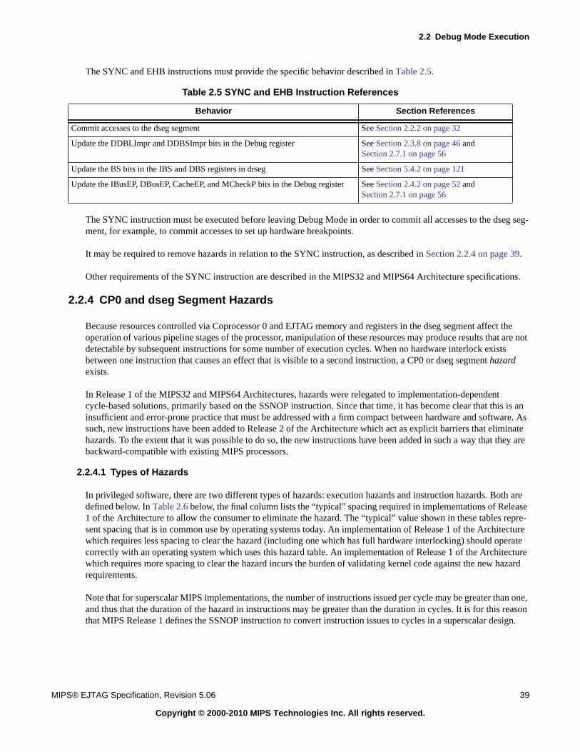
2.2 Debug Mode Execution
MIPS® EJTAG Specification, Revision 5.06 39
Copyright © 2000-2010 MIPS Technologies Inc. All rights reserved.
The SYNC and EHB instructions must provide the specific behavior described in Table 2.5.
The SYNC instruction must be executed before leaving Debug Mode in order to commit all accesses to the dseg seg-ment, for example, to commit accesses to set up hardware breakpoints.
It may be required to remove hazards in relation to the SYNC instruction, as described in Section 2.2.4 on page 39.
Other requirements of the SYNC instruction are described in the MIPS32 and MIPS64 Architecture specifications.
2.2.4 CP0 and dseg Segment Hazards
Because resources controlled via Coprocessor 0 and EJTAG memory and registers in the dseg segment affect theoperation of various pipeline stages of the processor, manipulation of these resources may produce results that are notdetectable by subsequent instructions for some number of execution cycles. When no hardware interlock existsbetween one instruction that causes an effect that is visible to a second instruction, a CP0 or dseg segment hazardexists.
In Release 1 of the MIPS32 and MIPS64 Architectures, hazards were relegated to implementation-dependentcycle-based solutions, primarily based on the SSNOP instruction. Since that time, it has become clear that this is aninsufficient and error-prone practice that must be addressed with a firm compact between hardware and software. Assuch, new instructions have been added to Release 2 of the Architecture which act as explicit barriers that eliminatehazards. To the extent that it was possible to do so, the new instructions have been added in such a way that they arebackward-compatible with existing MIPS processors.
2.2.4.1 Types of Hazards
In privileged software, there are two different types of hazards: execution hazards and instruction hazards. Both aredefined below. In Table 2.6 below, the final column lists the “typical” spacing required in implementations of Release1 of the Architecture to allow the consumer to eliminate the hazard. The “typical” value shown in these tables repre-sent spacing that is in common use by operating systems today. An implementation of Release 1 of the Architecturewhich requires less spacing to clear the hazard (including one which has full hardware interlocking) should operatecorrectly with an operating system which uses this hazard table. An implementation of Release 1 of the Architecturewhich requires more spacing to clear the hazard incurs the burden of validating kernel code against the new hazardrequirements.
Note that for superscalar MIPS implementations, the number of instructions issued per cycle may be greater than one,and thus that the duration of the hazard in instructions may be greater than the duration in cycles. It is for this reasonthat MIPS Release 1 defines the SSNOP instruction to convert instruction issues to cycles in a superscalar design.
Table 2.5 SYNC and EHB Instruction References
Behavior Section References
Commit accesses to the dseg segment See Section 2.2.2 on page 32
Update the DDBLImpr and DDBSImpr bits in the Debug register See Section 2.3.8 on page 46 andSection 2.7.1 on page 56
Update the BS bits in the IBS and DBS registers in drseg See Section 5.4.2 on page 121
Update the IBusEP, DBusEP, CacheEP, and MCheckP bits in the Debug register See Section 2.4.2 on page 52 andSection 2.7.1 on page 56
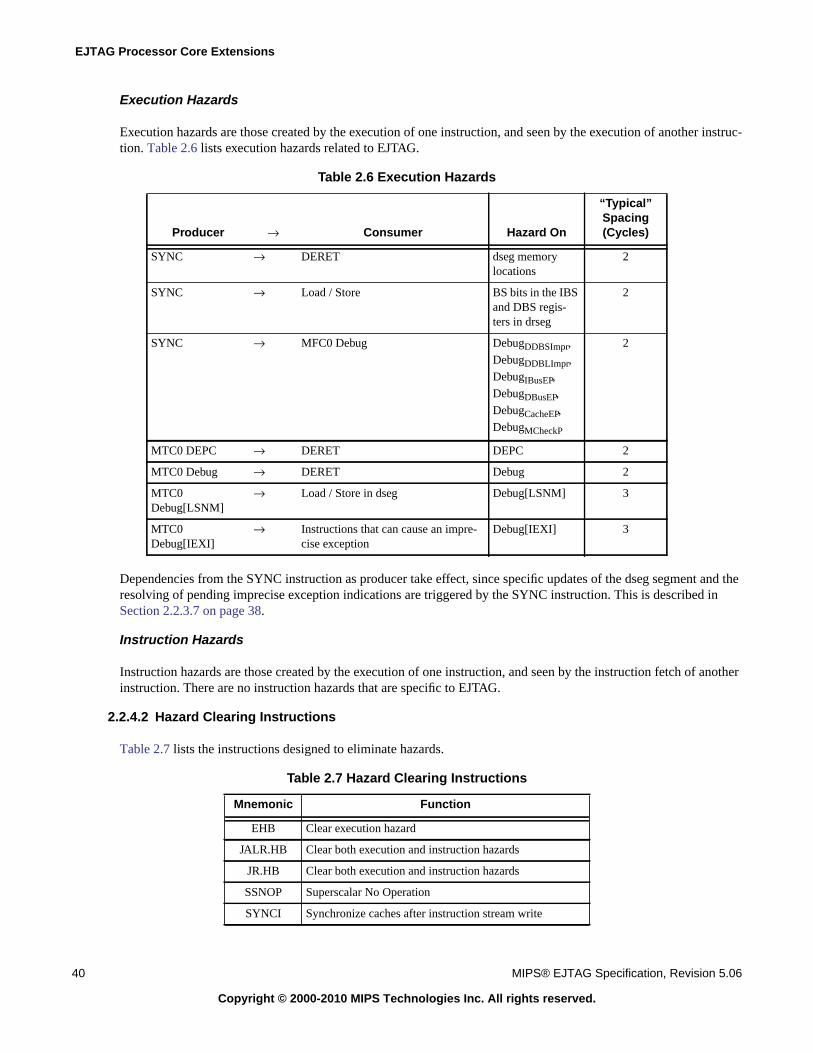
EJTAG Processor Core Extensions
40 MIPS® EJTAG Specification, Revision 5.06
Copyright © 2000-2010 MIPS Technologies Inc. All rights reserved.
Execution Hazards
Execution hazards are those created by the execution of one instruction, and seen by the execution of another instruc-tion. Table 2.6 lists execution hazards related to EJTAG.
Dependencies from the SYNC instruction as producer take effect, since specific updates of the dseg segment and theresolving of pending imprecise exception indications are triggered by the SYNC instruction. This is described inSection 2.2.3.7 on page 38.
Instruction Hazards
Instruction hazards are those created by the execution of one instruction, and seen by the instruction fetch of anotherinstruction. There are no instruction hazards that are specific to EJTAG.
2.2.4.2 Hazard Clearing Instructions
Table 2.7 lists the instructions designed to eliminate hazards.
Table 2.6 Execution Hazards
Producer → Consumer Hazard On
“Typical”Spacing(Cycles)
SYNC → DERET dseg memorylocations
2
SYNC → Load / Store BS bits in the IBSand DBS regis-ters in drseg
2
SYNC → MFC0 Debug DebugDDBSImpr,
DebugDDBLImpr,
DebugIBusEP,
DebugDBusEP,
DebugCacheEP,
DebugMCheckP
2
MTC0 DEPC → DERET DEPC 2
MTC0 Debug → DERET Debug 2
MTC0Debug[LSNM]
→ Load / Store in dseg Debug[LSNM] 3
MTC0Debug[IEXI]
→ Instructions that can cause an impre-cise exception
Debug[IEXI] 3
Table 2.7 Hazard Clearing Instructions
Mnemonic Function
EHB Clear execution hazard
JALR.HB Clear both execution and instruction hazards
JR.HB Clear both execution and instruction hazards
SSNOP Superscalar No Operation
SYNCI Synchronize caches after instruction stream write
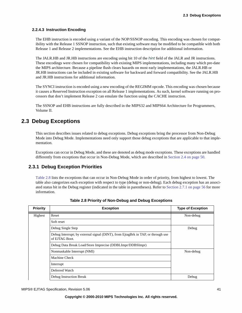
2.3 Debug Exceptions
MIPS® EJTAG Specification, Revision 5.06 41
Copyright © 2000-2010 MIPS Technologies Inc. All rights reserved.
2.2.4.3 Instruction Encoding
The EHB instruction is encoded using a variant of the NOP/SSNOP encoding. This encoding was chosen for compat-ibility with the Release 1 SSNOP instruction, such that existing software may be modified to be compatible with bothRelease 1 and Release 2 implementations. See the EHB instruction description for additional information.
The JALR.HB and JR.HB instructions are encoding using bit 10 of the hint field of the JALR and JR instructions.These encodings were chosen for compatibility with existing MIPS implementations, including many which pre-datethe MIPS architecture. Because a pipeline flush clears hazards on most early implementations, the JALR.HB orJR.HB instructions can be included in existing software for backward and forward compatibility. See the JALR.HBand JR.HB instructions for additional information.
The SYNCI instruction is encoded using a new encoding of the REGIMM opcode. This encoding was chosen becauseit causes a Reserved Instruction exception on all Release 1 implementations. As such, kernel software running on pro-cessors that don’t implement Release 2 can emulate the function using the CACHE instruction.
The SSNOP and EHB instructions are fully described in the MIPS32 and MIPS64 Architecture for Programmers,Volume II.
2.3 Debug Exceptions
This section describes issues related to debug exceptions. Debug exceptions bring the processor from Non-DebugMode into Debug Mode. Implementations need only support those debug exceptions that are applicable to that imple-mentation.
Exceptions can occur in Debug Mode, and these are denoted as debug mode exceptions. These exceptions are handleddifferently from exceptions that occur in Non-Debug Mode, which are described in Section 2.4 on page 50.
2.3.1 Debug Exception Priorities
Table 2.8 lists the exceptions that can occur in Non-Debug Mode in order of priority, from highest to lowest. Thetable also categorizes each exception with respect to type (debug or non-debug). Each debug exception has an associ-ated status bit in the Debug register (indicated in the table in parentheses). Refer to Section 2.7.1 on page 56 for moreinformation.
Table 2.8 Priority of Non-Debug and Debug Exceptions
Priority Exception Type of Exception
Highest Reset Non-debug
Soft reset
Debug Single Step Debug
Debug Interrupt; by external signal (DINT), from EjtagBrk in TAP, or through useof EJTAG Boot.
Debug Data Break Load/Store Imprecise (DDBLImpr/DDBSImpr)
Nonmaskable Interrupt (NMI) Non-debug
Machine Check
Interrupt
Deferred Watch
Debug Instruction Break Debug
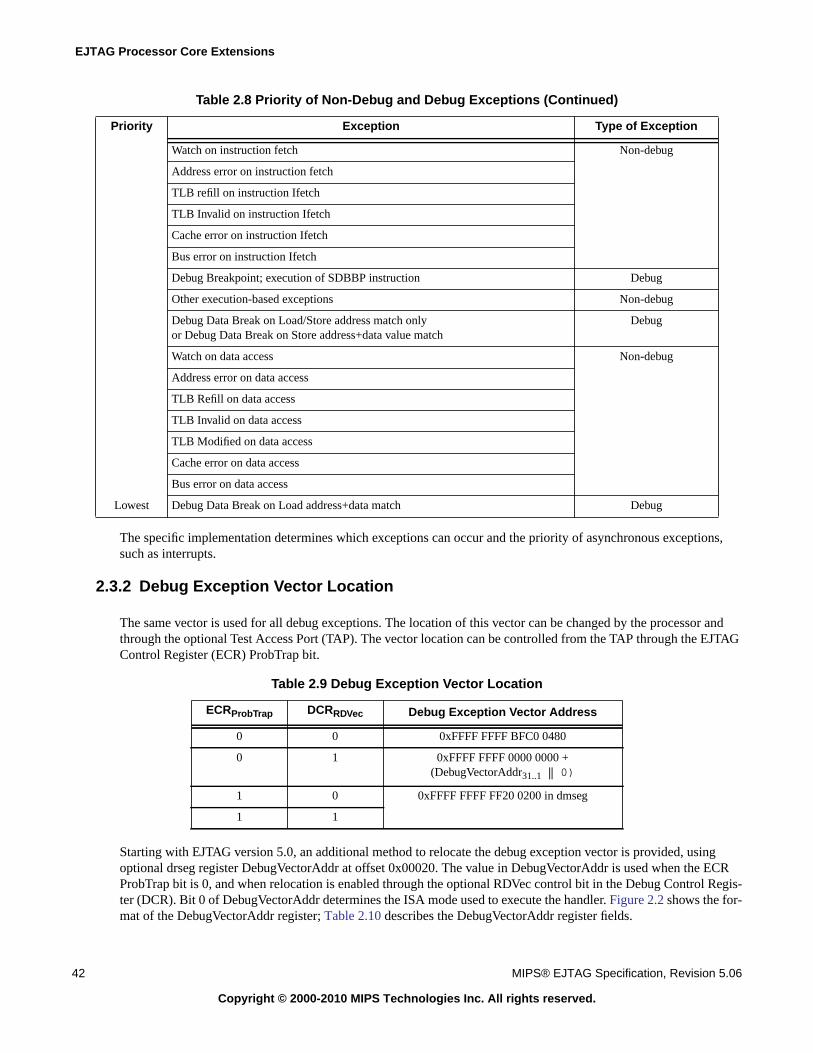
EJTAG Processor Core Extensions
42 MIPS® EJTAG Specification, Revision 5.06
Copyright © 2000-2010 MIPS Technologies Inc. All rights reserved.
The specific implementation determines which exceptions can occur and the priority of asynchronous exceptions,such as interrupts.
2.3.2 Debug Exception Vector Location
The same vector is used for all debug exceptions. The location of this vector can be changed by the processor andthrough the optional Test Access Port (TAP). The vector location can be controlled from the TAP through the EJTAGControl Register (ECR) ProbTrap bit.
Starting with EJTAG version 5.0, an additional method to relocate the debug exception vector is provided, usingoptional drseg register DebugVectorAddr at offset 0x00020. The value in DebugVectorAddr is used when the ECRProbTrap bit is 0, and when relocation is enabled through the optional RDVec control bit in the Debug Control Regis-ter (DCR). Bit 0 of DebugVectorAddr determines the ISA mode used to execute the handler. Figure 2.2 shows the for-mat of the DebugVectorAddr register; Table 2.10 describes the DebugVectorAddr register fields.
Watch on instruction fetch Non-debug
Address error on instruction fetch
TLB refill on instruction Ifetch
TLB Invalid on instruction Ifetch
Cache error on instruction Ifetch
Bus error on instruction Ifetch
Debug Breakpoint; execution of SDBBP instruction Debug
Other execution-based exceptions Non-debug
Debug Data Break on Load/Store address match onlyor Debug Data Break on Store address+data value match
Debug
Watch on data access Non-debug
Address error on data access
TLB Refill on data access
TLB Invalid on data access
TLB Modified on data access
Cache error on data access
Bus error on data access
Lowest Debug Data Break on Load address+data match Debug
Table 2.9 Debug Exception Vector Location
ECRProbTrap DCRRDVec Debug Exception Vector Address
0 0 0xFFFF FFFF BFC0 0480
0 1 0xFFFF FFFF 0000 0000 +(DebugVectorAddr31..1 || 0)
1 0 0xFFFF FFFF FF20 0200 in dmseg
1 1
Table 2.8 Priority of Non-Debug and Debug Exceptions (Continued)
Priority Exception Type of Exception
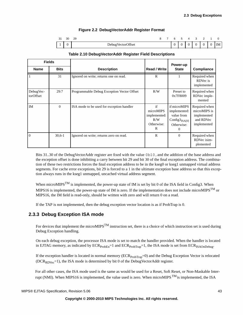
2.3 Debug Exceptions
MIPS® EJTAG Specification, Revision 5.06 43
Copyright © 2000-2010 MIPS Technologies Inc. All rights reserved.
Figure 2.2 DebugVectorAddr Register Format
Bits 31..30 of the DebugVectorAddr register are fixed with the value 0b10,and the addition of the base address andthe exception offset is done inhibiting a carry between bit 29 and bit 30 of the final exception address. The combina-tion of these two restrictions forces the final exception address to be in the kseg0 or kseg1 unmapped virtual addresssegments. For cache error exceptions, bit 29 is forced to a 1 in the ultimate exception base address so that this excep-tion always runs in the kseg1 unmapped, uncached virtual address segment.
When microMIPSTM is implemented, the power-up state of IM is set by bit 0 of the ISA field in Config3. When
MIPS16 is implemented, the power-up state of IM is zero. If the implementation does not include microMIPSTM orMIPS16, the IM field is read-only, should be written with zero and will return 0 on a read.
If the TAP is not implemented, then the debug exception vector location is as if ProbTrap is 0.
2.3.3 Debug Exception ISA mode
For devices that implement the microMIPSTM instruction set, there is a choice of which instruction set is used duringDebug Exception handling.
On each debug exception, the processor ISA mode is set to match the handler provided. When the handler is locatedin EJTAG memory, as indicated by ECRProbEn=1 and ECRProbTrap=1, the ISA mode is set from ECRISAOnDebug.
If the exception handler is located in normal memory (ECRProbTrap=0) and the Debug Exception Vector is relocated(DCRRDVec=1), the ISA mode is determined by bit 0 of the DebugVectorAddr register.
For all other cases, the ISA mode used is the same as would be used for a Reset, Soft Reset, or Non-Maskable Inter-
rupt (NMI). When MIPS16 is implemented, the value used is zero. When microMIPS TM is implemented, the ISA
31 30 29 8 7 6 5 4 3 2 1 0
1 0 DebugVectorOffset 0 0 0 0 0 0 IM
Table 2.10 DebugVectorAddr Register Field Descriptions
Fields
Description Read / WritePower-up
State ComplianceName Bits
1 31 Ignored on write; returns one on read. R 1 Required whenRDVec is
implemented
DebugVec-torOffset
29:7 Programmable Debug Exception Vector Offset R/W Preset to0x7F8009
Required whenRDVec imple-
mented
IM 0 ISA mode to be used for exception handler ifmicroMIPS
implemented:R/W
Otherwise:R
if microMIPSimplemented:
value fromConfig3ISA[0]
Otherwise:0
Required whenmicroMIPS isimplementedand RDVec
implemented
0 30,6-1 Ignored on write; returns zero on read. R 0 Required whenRDVec isim-plemented
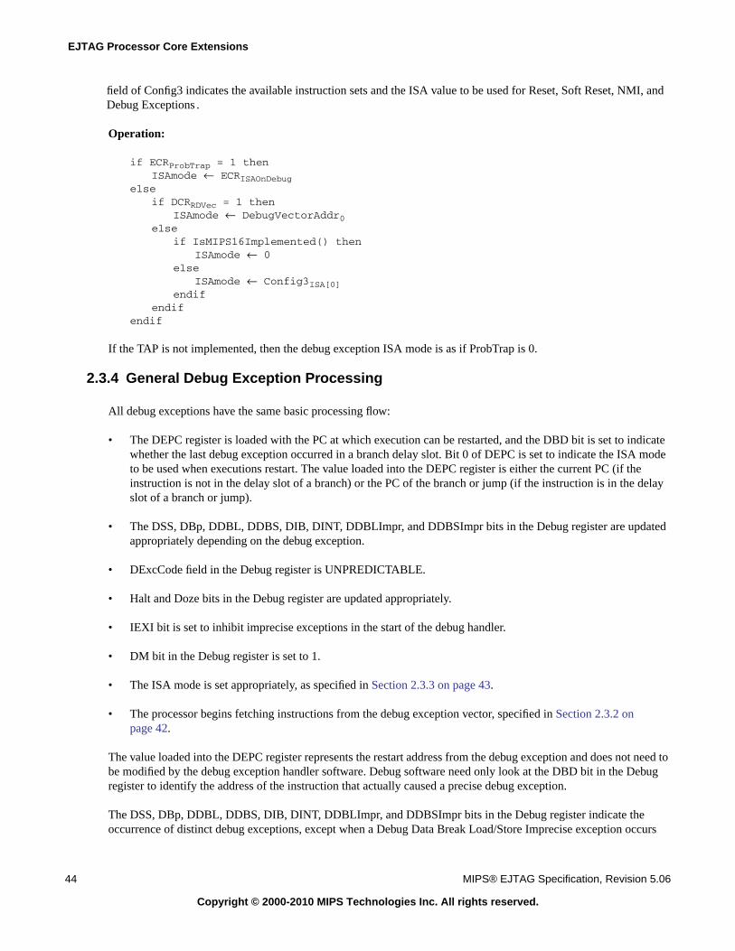
EJTAG Processor Core Extensions
44 MIPS® EJTAG Specification, Revision 5.06
Copyright © 2000-2010 MIPS Technologies Inc. All rights reserved.
field of Config3 indicates the available instruction sets and the ISA value to be used for Reset, Soft Reset, NMI, andDebug Exceptions .
Operation:
if ECRProbTrap = 1 thenISAmode ← ECRISAOnDebug
elseif DCRRDVec = 1 then
ISAmode ← DebugVectorAddr0else
if IsMIPS16Implemented() thenISAmode ← 0
elseISAmode ← Config3ISA[0]
endifendif
endif
If the TAP is not implemented, then the debug exception ISA mode is as if ProbTrap is 0.
2.3.4 General Debug Exception Processing
All debug exceptions have the same basic processing flow:
• The DEPC register is loaded with the PC at which execution can be restarted, and the DBD bit is set to indicatewhether the last debug exception occurred in a branch delay slot. Bit 0 of DEPC is set to indicate the ISA modeto be used when executions restart. The value loaded into the DEPC register is either the current PC (if theinstruction is not in the delay slot of a branch) or the PC of the branch or jump (if the instruction is in the delayslot of a branch or jump).
• The DSS, DBp, DDBL, DDBS, DIB, DINT, DDBLImpr, and DDBSImpr bits in the Debug register are updatedappropriately depending on the debug exception.
• DExcCode field in the Debug register is UNPREDICTABLE.
• Halt and Doze bits in the Debug register are updated appropriately.
• IEXI bit is set to inhibit imprecise exceptions in the start of the debug handler.
• DM bit in the Debug register is set to 1.
• The ISA mode is set appropriately, as specified in Section 2.3.3 on page 43.
• The processor begins fetching instructions from the debug exception vector, specified in Section 2.3.2 onpage 42.
The value loaded into the DEPC register represents the restart address from the debug exception and does not need tobe modified by the debug exception handler software. Debug software need only look at the DBD bit in the Debugregister to identify the address of the instruction that actually caused a precise debug exception.
The DSS, DBp, DDBL, DDBS, DIB, DINT, DDBLImpr, and DDBSImpr bits in the Debug register indicate theoccurrence of distinct debug exceptions, except when a Debug Data Break Load/Store Imprecise exception occurs
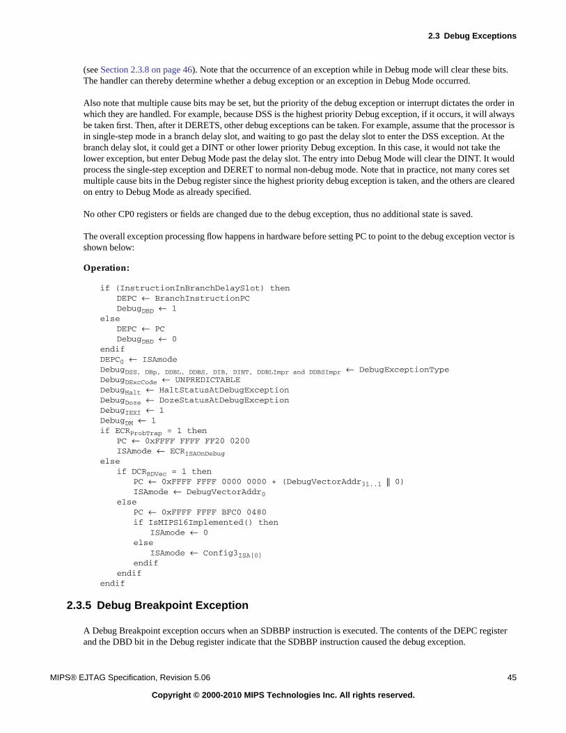
2.3 Debug Exceptions
MIPS® EJTAG Specification, Revision 5.06 45
Copyright © 2000-2010 MIPS Technologies Inc. All rights reserved.
(see Section 2.3.8 on page 46). Note that the occurrence of an exception while in Debug mode will clear these bits.The handler can thereby determine whether a debug exception or an exception in Debug Mode occurred.
Also note that multiple cause bits may be set, but the priority of the debug exception or interrupt dictates the order inwhich they are handled. For example, because DSS is the highest priority Debug exception, if it occurs, it will alwaysbe taken first. Then, after it DERETS, other debug exceptions can be taken. For example, assume that the processor isin single-step mode in a branch delay slot, and waiting to go past the delay slot to enter the DSS exception. At thebranch delay slot, it could get a DINT or other lower priority Debug exception. In this case, it would not take thelower exception, but enter Debug Mode past the delay slot. The entry into Debug Mode will clear the DINT. It wouldprocess the single-step exception and DERET to normal non-debug mode. Note that in practice, not many cores setmultiple cause bits in the Debug register since the highest priority debug exception is taken, and the others are clearedon entry to Debug Mode as already specified.
No other CP0 registers or fields are changed due to the debug exception, thus no additional state is saved.
The overall exception processing flow happens in hardware before setting PC to point to the debug exception vector isshown below:
Operation:
if (InstructionInBranchDelaySlot) thenDEPC ← BranchInstructionPCDebugDBD ← 1
elseDEPC ← PCDebugDBD ← 0
endifDEPC0 ← ISAmodeDebugDSS, DBp, DDBL, DDBS, DIB, DINT, DDBLImpr and DDBSImpr ← DebugExceptionTypeDebugDExcCode ← UNPREDICTABLEDebugHalt ← HaltStatusAtDebugExceptionDebugDoze ← DozeStatusAtDebugExceptionDebugIEXI ← 1DebugDM ← 1if ECRProbTrap = 1 then
PC ← 0xFFFF FFFF FF20 0200ISAmode ← ECRISAOnDebug
elseif DCRRDVec = 1 then
PC ← 0xFFFF FFFF 0000 0000 + (DebugVectorAddr31..1 || 0)ISAmode ← DebugVectorAddr0
elsePC ← 0xFFFF FFFF BFC0 0480if IsMIPS16Implemented() then
ISAmode ← 0else
ISAmode ← Config3ISA[0]endif
endifendif
2.3.5 Debug Breakpoint Exception
A Debug Breakpoint exception occurs when an SDBBP instruction is executed. The contents of the DEPC registerand the DBD bit in the Debug register indicate that the SDBBP instruction caused the debug exception.
EJTAG Processor Core Extensions
46 MIPS® EJTAG Specification, Revision 5.06
Copyright © 2000-2010 MIPS Technologies Inc. All rights reserved.
Debug Register Debug Status Bit Set
DBp
Additional State Saved
None
Entry Vector Used
Debug exception vector
2.3.6 Debug Instruction Break Exception
A Debug Instruction Break exception occurs when an instruction hardware breakpoint matches an executed instruc-tion. The DEPC register and DBD bit in the Debug register indicate the instruction that caused the instruction hard-ware breakpoint match. This exception can only occur if instruction hardware breakpoints are implemented (seeChapter 5, “Hardware Breakpoints” on page 111).
Debug Register Debug Status Bit Set
DIB
Additional State Saved
None
Entry Vector Used
Debug exception vector
2.3.7 Debug Data Break Load/Store Exception
A Debug Data Break Load/Store exception occurs when a data hardware breakpoint matches the load/store address ofan executed load/store instruction. The DEPC register and DBD bit in the Debug register indicate the load/storeinstruction that caused the data hardware breakpoint to match, as this is a precise debug exception. The load/storeinstruction that caused the debug exception has not completed (it has not updated the destination register or memorylocation), and the instruction therefore is executed on return from the debug handler. This exception can only occur ifdata hardware breakpoints with precise data breaks are implemented (see Chapter 5, “Hardware Breakpoints” onpage 111).
Debug Register Debug Status Bit Set
DDBL for a load instruction or DDBS for a store instruction
Additional State Saved
None
Entry Vector Used
Debug exception vector
2.3.8 Debug Data Break Load/Store Imprecise Exception
A Debug Data Break Load/Store Imprecise exception occurs when a data hardware breakpoint matches a load/storeaccess of an executed load/store instruction, if it is not possible to take a precise debug exception on the instruction.This case occurs when a data hardware breakpoint was set up with a value compare, and a load access did not returndata until after the load instruction had left the pipeline as for non-blocking loads. The DEPC register and the DBD
2.3 Debug Exceptions
MIPS® EJTAG Specification, Revision 5.06 47
Copyright © 2000-2010 MIPS Technologies Inc. All rights reserved.
bit in the Debug register indicate an instruction later in the execution flow instead of the load/store instruction thatcaused the data hardware breakpoint to match. The DDBLImpr/DDBSImpr bits in the Debug register indicate that aDebug Data Break Load/Store Imprecise exception occurred. The instruction that caused the Debug Data BreakLoad/Store Imprecise exception will have completed. It updates its destination register, and is not executed on returnfrom the debug handler. This exception can only occur if data hardware breakpoints with imprecise data breakpointsare implemented (see Chapter 5, “Hardware Breakpoints” on page 111).
Imprecise debug exceptions from data hardware breakpoints are indicated together with another debug exception ifthe load/store transaction that made the data hardware breakpoint match did not complete until after another debugexception occurred. In this case, the other debug exception was the cause of entering Debug Mode, so the DEPC reg-ister and the DBD bit in Debug register point to this instruction. DDBLImpr/DDBSImpr are set concurrently with thestatus bit for that debug exception.
The SYNC followed by appropriate spacing and the EHB instruction, (as described in Section 2.2.3.7 on page 38 andSection 2.2.4 on page 39) must be executed in Debug Mode before the DDBLImpr and DDBSImpr bits in the Debugregister and the BS bits for the data hardware breakpoint are respectively read in order to ensure that all imprecisebreaks are resolved and the bits are fully updated. A match of the data hardware breakpoint is indicated inDDBLImpr/DDBSImpr so the debug handler can handle this together with the debug exception.
This scheme ensures that all breakpoints matching due to code executed before the debug exception are indicated bythe DDBLImpr, DDBSImpr, and BS bits for the following debug handler. Matches are neither queued nor do theycause debug exceptions at a later point. A debug exception occurring later than the debug exception handler is there-fore caused by code executed in Non-Debug Mode after the debug exception handler.
Debug Register Debug Status Bit Set
DDBLImpr for a load instruction or DDBSImpr for a store instruction
Additional State Saved
None
Entry Vector Used
Debug exception vector
2.3.9 Debug Single Step Exception
When single-step mode is enabled, a Debug Single Step exception occurs each time the processor has taken a singleexecution step in Non-Debug Mode. An execution step is a single instruction, or an instruction pair consisting of ajump/branch instruction and the instruction in the associated delay slot. The SSt bit in the Debug register enablesDebug Single Step exceptions. They are disabled on the first execution step after a DERET.
The DEPC register points to the instruction on which the Debug Single Step exception occurred, which is also thenext instruction to execute when returning from Debug Mode. The debug software can examine the system statebefore this instruction is executed. Thus the DEPC will not point to the instruction(s) that have just executed in theexecution step, but rather the instruction following the execution step. The Debug Single Step exception never occurson an instruction in a jump/branch delay slot, because the jump/branch and the instruction in the delay slot are alwaysexecuted in one execution step; thus the DBD bit in the Debug register is never set for a Debug Single Step exception.
Exceptions occurring on the instruction(s) in the execution step are taken regardless, so if a non-debug exceptionoccurs (other than reset or soft reset), a Debug Single Step exception is taken on the first instruction in the non-debugexception handler. The non-debug exception occurs during the execution step, and the instruction(s) that received anon-debug exception counts as the execution step.
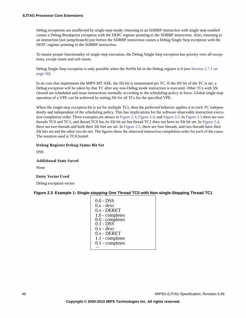
EJTAG Processor Core Extensions
48 MIPS® EJTAG Specification, Revision 5.06
Copyright © 2000-2010 MIPS Technologies Inc. All rights reserved.
Debug exceptions are unaffected by single-step mode; returning to an SDBBP instruction with single step enabledcauses a Debug Breakpoint exception with the DEPC register pointing to the SDBBP instruction. Also, returning toan instruction (not jump/branch) just before the SDBBP instruction causes a Debug Single Step exception with theDEPC register pointing to the SDBBP instruction.
To ensure proper functionality of single-step execution, the Debug Single Step exception has priority over all excep-tions, except resets and soft resets.
Debug Single Step exception is only possible when the NoSSt bit in the Debug register is 0 (see Section 2.7.1 onpage 56).
In an core that implements the MIPS MT ASE, the SSt bit is instantiated per TC. If the SSt bit of the TC is set, aDebug exception will be taken by that TC after any non-Debug mode instruction is executed. Other TCs with SStcleared are scheduled and issue instructions normally according to the scheduling policy in force. Global single-stepoperation of a VPE can be achieved by setting SSt for all TCs for the specified VPE.
When the single-step exception bit is set for multiple TCs, then the preferred behavior applies it to each TC indepen-dently and independent of the scheduling policy. This has implications for the software observable instruction execu-tion completion order. Three examples are shown in Figure 2.3, Figure 2.4, and Figure 2.5. In Figure 2.3 there are twothreads TC0 and TC1, and thread TC0 has its SSt bit set but thread TC1 does not have its SSt bit set. In Figure 2.4,there are two threads and both their SSt bits are set. In Figure 2.5, there are four threads, and two threads have theirSSt bits set and the other two do not. The figures show the observed instruction completion order for each of the cases.The notation used is TC#.Instn#.
Debug Register Debug Status Bit Set
DSS
Additional State Saved
None
Entry Vector Used
Debug exception vector
Figure 2.3 Example 1: Single-stepping One Thread TC0 with Non-single-Stepping Thread TC1
0.0 - DSS0.x - dexc0.x - DERET1.0 - completes
0.1 - DSS0.x - dexc0.x - DERET1.1 - completes0.1 - completes
0.0 - completes
...

2.3 Debug Exceptions
MIPS® EJTAG Specification, Revision 5.06 49
Copyright © 2000-2010 MIPS Technologies Inc. All rights reserved.
Figure 2.4 Example 2: Single-stepping Two Threads TC0 and TC1
Figure 2.5 Example 3: Single-stepping Two Threads TC0 and TC1 with Other Threads TC2 and TC3
2.3.10 Debug Interrupt Exception
The Debug Interrupt exception is an asynchronous debug exception that is taken as soon as possible, but with no spe-cific relation to the executed instructions. The DEPC register and the DBD bit in the Debug register reference theinstruction at which execution can be resumed after Debug Interrupt exception service.
Debug interrupt requests are ignored when the processor is in Debug Mode, and pending requests are cleared whenthe processor takes any debug exception, including debug exceptions other than Debug Interrupt exceptions.
A debug interrupt restarts the pipeline if stopped by a WAIT instruction and the processor clock is restarted if it wasstopped due to a low-power mode.
Debug Register Debug Status Bit Set
DINT
0.0 - DSS0.x - dexc handler0.x - DERET1.0 - DSS1.x - dexc handler1.x - DERET0.0 - completes1.0 - completes0.1 - DSS0.x - dexc handler0.x - DERET...
0.0 - DSS0.x - dexc handler0.x - DERET1.0 - completes2.0 - DSS2.x - dexc handler2.x - DERET3.0 - completes0.0 - completes1.1 - completes2.0 - completes3.1 - completes0.1 - DSS0.x - dexc handler0.x - DERET1.2 - completes...
EJTAG Processor Core Extensions
50 MIPS® EJTAG Specification, Revision 5.06
Copyright © 2000-2010 MIPS Technologies Inc. All rights reserved.
Additional State Saved
None
Entry Vector Used
Debug exception vector
The possible sources for debug interrupts depend on the implementation. The following sources can cause DebugInterrupt exceptions:
• The DINT signal from the probe
The optional DINT signal from the probe can request a debug interrupt on a low (0) to high (1) transition. TheDINTsup bit in the Implementation register in the Test Access Port (TAP) indicates whether the DINT signalfrom the probe to the target processor is implemented (see Section 4.5.2 on page 90). The timing requirementsfor the DINT signal are shown in Section 10.2.2 on page 180.
The DINT signal can be synchronized to the processor clock domain before edge detection while still observingthe required timing of the DINT signal. If the CPU clock speed or clocking scheme is such that the required tim-ing does not leave enough time for synchronization or clock wake-up, then the DINT pulse is extended by the tar-get system in the processor.
The EjtagBrk bit in the EJTAG Control register provides similar functionality similar to DINT from the probe,but with higher latency.
• The EjtagBrk Bit in the EJTAG Control Register
The EjtagBrk bit in the EJTAG Control register requests a Debug Interrupt exception when set (see Section 4.5.5on page 96).
• A debug boot by EJTAGBOOT
The EJTAGBOOT feature causes code to be fetched from the debug interrupt vector immediately after a reset orsoft reset has occurred (see Section 2.6.1 on page 54 and Section 4.4.2 on page 87).
• An implementation-specific debug interrupt signal to the processor
Through the availability of an optional debug interrupt request signal to the processor system, an external devicecan request a Debug Interrupt exception, for example, when a signal goes from deasserted to asserted.
2.4 Debug Mode Exceptions
The handling of exceptions generated in Debug Mode, other than through resets and soft resets, differs from thoseexceptions generated in Non-Debug Mode in that only the Debug and DEPC registers are updated. All other CP0 reg-isters are unchanged by an exception taken in Debug Mode. The exception vector is equal to the debug exception vec-tor (see Section 2.3.2 on page 42), and the processor stays in Debug Mode.
Reset and soft reset are handled as when occurring in Non-Debug Mode (see Section 2.6 on page 54).
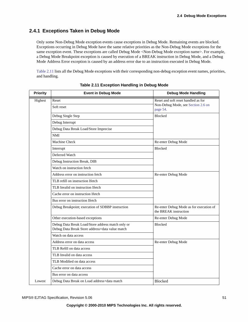
2.4 Debug Mode Exceptions
MIPS® EJTAG Specification, Revision 5.06 51
Copyright © 2000-2010 MIPS Technologies Inc. All rights reserved.
2.4.1 Exceptions Taken in Debug Mode
Only some Non-Debug Mode exception events cause exceptions in Debug Mode. Remaining events are blocked.Exceptions occurring in Debug Mode have the same relative priorities as the Non-Debug Mode exceptions for thesame exception event. These exceptions are called Debug Mode <Non-Debug Mode exception name>. For example,a Debug Mode Breakpoint exception is caused by execution of a BREAK instruction in Debug Mode, and a DebugMode Address Error exception is caused by an address error due to an instruction executed in Debug Mode.
Table 2.11 lists all the Debug Mode exceptions with their corresponding non-debug exception event names, priorities,and handling.
Table 2.11 Exception Handling in Debug Mode
Priority Event in Debug Mode Debug Mode Handling
Highest Reset Reset and soft reset handled as forNon-Debug Mode, see Section 2.6 onpage 54.
Soft reset
Debug Single Step Blocked
Debug Interrupt
Debug Data Break Load/Store Imprecise
NMI
Machine Check Re-enter Debug Mode
Interrupt Blocked
Deferred Watch
Debug Instruction Break, DIB
Watch on instruction fetch
Address error on instruction fetch Re-enter Debug Mode
TLB refill on instruction Ifetch
TLB Invalid on instruction Ifetch
Cache error on instruction Ifetch
Bus error on instruction Ifetch
Debug Breakpoint; execution of SDBBP instruction Re-enter Debug Mode as for execution ofthe BREAK instruction
Other execution-based exceptions Re-enter Debug Mode
Debug Data Break Load/Store address match only orDebug Data Break Store address+data value match
Blocked
Watch on data access
Address error on data access Re-enter Debug Mode
TLB Refill on data access
TLB Invalid on data access
TLB Modified on data access
Cache error on data access
Bus error on data access
Lowest Debug Data Break on Load address+data match Blocked
EJTAG Processor Core Extensions
52 MIPS® EJTAG Specification, Revision 5.06
Copyright © 2000-2010 MIPS Technologies Inc. All rights reserved.
The specific implementation determines which exceptions can occur. Exceptions that are blocked in Debug Mode aresimply ignored, not causing updates in any state.
Handling of the exceptions causing Debug Mode re-enter are described below.
2.4.2 Exceptions on Imprecise Errors
Exceptions on imprecise errors are possible in Debug Mode due to a bus error on an instruction fetch or data access,cache error, or machine check.
The IEXI bit in the Debug register blocks imprecise error exceptions on entry or re-entry into Debug Mode. They canbe re-enabled by the debug exception handler after sufficient context has been saved to allow a safe re-entry intoDebug Mode and the debug handler.
Pending exceptions due to instruction fetch bus errors, data access bus errors, cache errors, and machine checks areindicated and controlled by the IBusEP, DBusEP, CacheEP and MCheckP bit in the Debug register.
The SYNC instruction, followed by appropriate spacing and the EHB instruction, (as described in Section 2.2.3.7 onpage 38 and Section 2.2.4 on page 39) must be executed in Debug Mode before the IBusEP, DBusEP, CacheEP, andMCheckP bits are read in order to ensure that all pending causes for imprecise errors are resolved and all bits are fullyupdated.
Those bits required to handle the possible imprecise errors in an implementation are implemented as R/W; otherwise,they are read only.
2.4.3 Debug Mode Exception Processing
All exceptions that are allowed in Debug Mode (except for reset and soft reset) have the same basic processing flow:
• The DEPC register is loaded with the PC at which execution can be restarted, and the DBD bit is set to indicatewhether the last debug exception occurred in a branch delay slot. If the multiple ISAs are supported, Bit 0 ofDEPC is set to indicate the ISA mode to be used when executions restart. The value loaded into the DEPC regis-ter is either the current PC (if the instruction is not in the delay slot of a branch) or the PC of the branch or jump(if the instruction is in the delay slot of a branch or jump).
• The DSS, DBp, DDBL, DDBS, DIB, DINT, DDBLImpr, and DDBSImpr bits in the Debug register are allcleared to differentiate from debug exceptions where at least one of the bits are set.
• The DExcCode field in the Debug register is updated to indicate the type of exception that occurred.
• The Halt and Doze bits in the Debug register are UNPREDICTABLE.
• The IEXI bit is set to inhibit imprecise exceptions at the start of the debug handler.
• The DM bit in the Debug register is unchanged, leaving the processor in Debug Mode.
• The ISA mode is set appropriately, as specified in Section 2.3.3 on page 43.
• The processor is started at the debug exception vector, specified in Section 2.3.2 on page 42.
The value loaded into the DEPC register represents the restart address for the exception; typically debug softwaredoes not need to modify this value at the location of the debug exception. Debug software need not look at the DBD
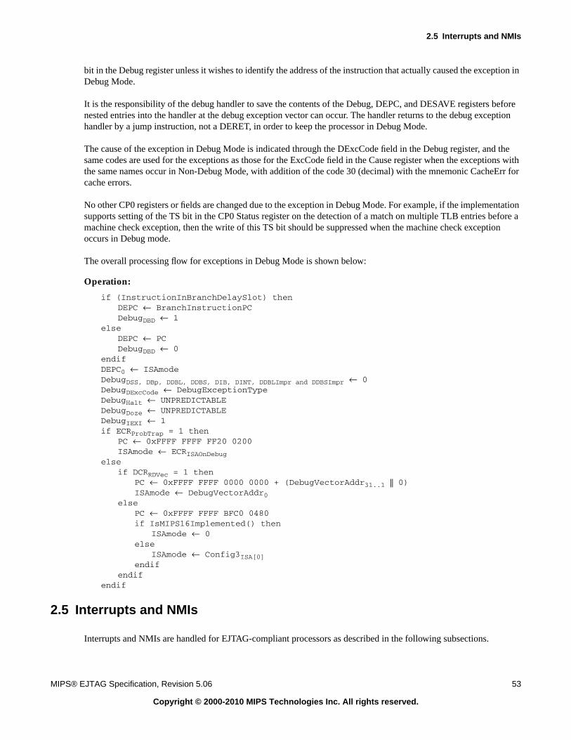
2.5 Interrupts and NMIs
MIPS® EJTAG Specification, Revision 5.06 53
Copyright © 2000-2010 MIPS Technologies Inc. All rights reserved.
bit in the Debug register unless it wishes to identify the address of the instruction that actually caused the exception inDebug Mode.
It is the responsibility of the debug handler to save the contents of the Debug, DEPC, and DESAVE registers beforenested entries into the handler at the debug exception vector can occur. The handler returns to the debug exceptionhandler by a jump instruction, not a DERET, in order to keep the processor in Debug Mode.
The cause of the exception in Debug Mode is indicated through the DExcCode field in the Debug register, and thesame codes are used for the exceptions as those for the ExcCode field in the Cause register when the exceptions withthe same names occur in Non-Debug Mode, with addition of the code 30 (decimal) with the mnemonic CacheErr forcache errors.
No other CP0 registers or fields are changed due to the exception in Debug Mode. For example, if the implementationsupports setting of the TS bit in the CP0 Status register on the detection of a match on multiple TLB entries before amachine check exception, then the write of this TS bit should be suppressed when the machine check exceptionoccurs in Debug mode.
The overall processing flow for exceptions in Debug Mode is shown below:
Operation:
if (InstructionInBranchDelaySlot) thenDEPC ← BranchInstructionPCDebugDBD ← 1
elseDEPC ← PCDebugDBD ← 0
endifDEPC0 ← ISAmodeDebugDSS, DBp, DDBL, DDBS, DIB, DINT, DDBLImpr and DDBSImpr ← 0DebugDExcCode ← DebugExceptionTypeDebugHalt ← UNPREDICTABLEDebugDoze ← UNPREDICTABLEDebugIEXI ← 1if ECRProbTrap = 1 then
PC ← 0xFFFF FFFF FF20 0200ISAmode ← ECRISAOnDebug
elseif DCRRDVec = 1 then
PC ← 0xFFFF FFFF 0000 0000 + (DebugVectorAddr31..1 || 0)ISAmode ← DebugVectorAddr0
elsePC ← 0xFFFF FFFF BFC0 0480if IsMIPS16Implemented() then
ISAmode ← 0else
ISAmode ← Config3ISA[0]endif
endifendif
2.5 Interrupts and NMIs
Interrupts and NMIs are handled for EJTAG-compliant processors as described in the following subsections.
EJTAG Processor Core Extensions
54 MIPS® EJTAG Specification, Revision 5.06
Copyright © 2000-2010 MIPS Technologies Inc. All rights reserved.
2.5.1 Interrupts
Interrupts are requested through either asserted external hardware signals or internal software-controllable bits. Inter-rupt exceptions are disabled when any of the following conditions are true:
• The processor is operating in Debug Mode
• The Interrupt Enable (IntE) bit in the Debug Control Register (DCR) is cleared (see Section Table 3.1 “DCRRegister Field Descriptions”)
• A non-EJTAG related mechanism disables the interrupt exception
A pending interrupt is indicated through the Cause register, even if Interrupt exceptions are disabled.
2.5.2 NMIs
An NMI is requested on the asserting edge of the NMI signal to the processor, and an internal indicator holds the NMIrequest until the NMI exception is actually taken.
NMI exceptions are disabled when either of the following is true:
• The Processor is operating in Debug Mode
• The NMI Enable (NMIE) bit in the Debug Control Register (DCR) is cleared, see Section Table 3.1 “DCRRegister Field Descriptions”
If an asserting edge on the NMI signal to the processor is detected while NMI exception is disabled, then the NMIrequest is held pending and is deferred until NMI exceptions are no longer disabled.
A pending NMI is indicated in the NMIpend bit in the DCR even if NMI exceptions are disabled.
2.6 Reset and Soft Reset of Processor
This section covers the handling of issues with respect to resets and soft resets. For EJTAG features, there are no dif-ference between a reset and a soft reset occurring to the processor; they behave identically in both Debug Mode andNon-Debug Mode. References to reset in the following therefore refers to both reset (hard reset) and soft reset.
2.6.1 EJTAGBOOT Feature
The EJTAGBOOT feature causes code to be fetched from the debug interrupt vector as a result of a reset instead ofthe code from regular reset exception vector.
The EJTAGBOOT feature only affects the address value which is loaded into the PC after the reset event. All of theother effects of a reset event - such as the clearing of RP, BEV, TS, SR, NMI and ERL fields within the Status registerand the updating of the ErrorEPC register still occur due to the reset event.
The location of the debug exception handler is controlled by the ProbTrap bit in the TAP Control register. When thisbit is set, the instructions for the debug exception handler are provided by the probe through the dmseg segment, tak-ing care of a situation where the normal memory system does not work properly.
2.7 EJTAG Coprocessor 0 Registers
MIPS® EJTAG Specification, Revision 5.06 55
Copyright © 2000-2010 MIPS Technologies Inc. All rights reserved.
Control and details of EJTAGBOOT are described in Section 4.4.2 on page 87 and Table 4.9 describes the ProbTrapbit in the EJTAG Control register.
2.6.2 Reset from Probe
While asserted, the RST* signal from the probe is required to generate a reset or soft reset to the system. The SRstEbit in the Debug Control Register does not mask this source. See Section 10.1.3 on page 177 for more information.
2.6.3 Processor Reset by Probe through Test Access Port
The PrRst bit in the EJTAG Control register can optionally cause a reset depending on the implementation. If a resetoccurs, then all parts of the system are reset, because partial resets are not allowed.
2.6.4 Reset Occurred Indication through Test Access Port
The Rocc bit in the EJTAG Control register is set at both reset and soft reset in order to indicate the event to the probe.
Refer to Section 4.5.5 on page 96 for more information on the EJTAG Control Register.
2.6.5 Soft Reset Enable
The optional Soft Reset Enable (SRstE) bit in the Debug Control Register (DCR) can mask the soft reset signal out-side the processor. Because SRstE masks the soft reset signal before it arrives at the processor, there is no masking ofsoft reset within the processor itself.
2.6.6 Reset of Other Debug Features
The operation of processor resets and soft resets also apply to resets of the following:
• Debug Control Register (DCR), see Chapter 3, “Debug Control Register” on page 75
• Hardware Breakpoint, see Chapter 5, “Hardware Breakpoints” on page 111
• Test Access Port (TAP) EJTAG Control Register, see Chapter 4, “EJTAG Test Access Port” on page 81
2.7 EJTAG Coprocessor 0 Registers
The Coprocessor 0 registers for EJTAG are shown in Table 2.12. Each register is described in more detail in the fol-lowing subsections.
Table 2.12 Coprocessor 0 Registers for EJTAG
RegisterNumber Sel
RegisterName Function Reference
ComplianceLevel
23 0 Debug Debug indications and controls for the processor. See Section 2.7.1on page 56
Required
23 6 Debug2 Complex breakpoint status See Section2.7.2 on page 65
Required(EJTAG 4.00and higher)
EJTAG Processor Core Extensions
56 MIPS® EJTAG Specification, Revision 5.06
Copyright © 2000-2010 MIPS Technologies Inc. All rights reserved.
The CP0 instructions MTC0, MFC0, DMTC0, and DMFC0 work with the three EJTAG CP0 registers as per theMIPS32 and MIPS64 Architecture specifications.
Operation of the processor is UNDEFINED if the Debug, DEPC, or DESAVE registers are written from Non-DebugMode. The value of the Debug, DEPC, or DESAVE registers is UNPREDICTABLE when read from Non-DebugMode, unless otherwise explicitly stated in the individual register description. However, for test purposes, the imple-mentations can allow writes to and reads from the registers from Non-Debug Mode.
To avoid pipeline hazards, there must be an appropriate spacing, refer to Section 2.2.4 on page 39, between the updateof the Debug and DEPC registers by MTC0/DMTC0 and use of the new value. This applies for example to modifica-tion of the LSNM bit of the Debug register and a load/store affected by that bit.
In a processor implementing the MIPS MT ASE, each of the Coprocessor 0 EJTAG registers described above isinstantiated per VPE. The exception is the SSt and OffLine bits in the Debug register which is instantiated per-TC.
2.7.1 Debug Register (CP0 Register 23, Select 0)
Compliance Level: Required for EJTAG debug support.
The Debug register contains the cause of the most recent debug exception and exception in Debug Mode. It also con-trols single stepping. This register indicates low-power and clock states on debug exceptions, debug resources, andother internal states.
Only the DM bit and the EJTAGver field are valid when read from the Debug register in Non-Debug Mode; the valueof all other bits and fields is UNPREDICTABLE.
The following bits and fields are only updated on debug exceptions and/or exceptions in Debug Mode:
• DSS, DBp, DDBL, DDBS, DIB, DINT, DIBImpr, DDBLImpr, and DDBSImpr are updated on both debugexceptions and on exceptions in Debug Modes
• DExcCode is updated on exceptions in Debug Mode, and is undefined after a debug exception
• Halt and Doze are updated on a debug exception, and are undefined after an exception in Debug Mode. In the sit-uation where the processor is awakened from sleep or doze state by a hardware interrupt or other external event,and a debug exception is taken instead (for example, if single-stepping a WAIT instruction), the state of the Haltand Doze bits should be as if the hardware interrupt had not occurred. That is, these bits should indicate that thestate of the processor was in Halt or Doze respectively before the exception, ignoring that the interrupt timemight be between halt/doze and the debug exception.
• DBD is updated on both debug and on exceptions in Debug Modes
24 0 DEPC Program counter at last debug exception orexception in Debug Mode.
See Section 2.7.3on page 66
Required
31 0 DESAVE Debug exception save register. See Section 2.7.4on page 67
Required
Table 2.12 Coprocessor 0 Registers for EJTAG (Continued)
RegisterNumber Sel
RegisterName Function Reference
ComplianceLevel
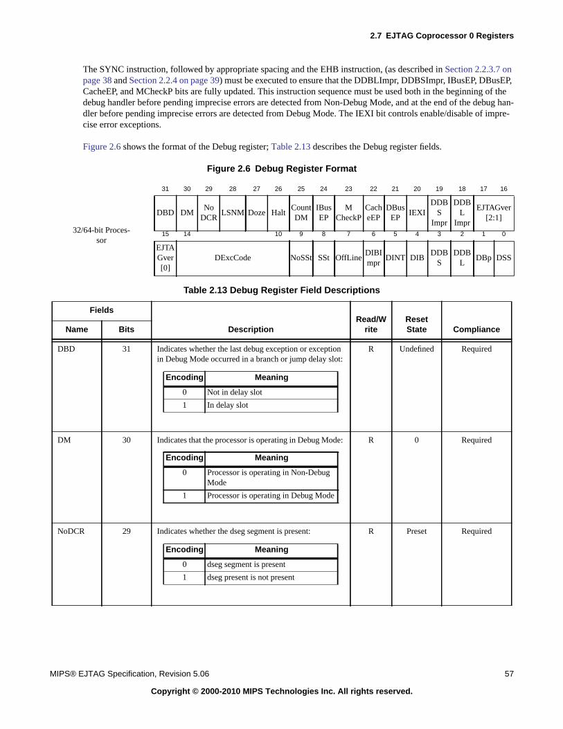
2.7 EJTAG Coprocessor 0 Registers
MIPS® EJTAG Specification, Revision 5.06 57
Copyright © 2000-2010 MIPS Technologies Inc. All rights reserved.
The SYNC instruction, followed by appropriate spacing and the EHB instruction, (as described in Section 2.2.3.7 onpage 38 and Section 2.2.4 on page 39) must be executed to ensure that the DDBLImpr, DDBSImpr, IBusEP, DBusEP,CacheEP, and MCheckP bits are fully updated. This instruction sequence must be used both in the beginning of thedebug handler before pending imprecise errors are detected from Non-Debug Mode, and at the end of the debug han-dler before pending imprecise errors are detected from Debug Mode. The IEXI bit controls enable/disable of impre-cise error exceptions.
Figure 2.6 shows the format of the Debug register; Table 2.13 describes the Debug register fields.
Figure 2.6 Debug Register Format
31 30 29 28 27 26 25 24 23 22 21 20 19 18 17 16
32/64-bit Proces-sor
DBD DMNo
DCRLSNM Doze Halt
CountDM
IBusEP
MCheckP
CacheEP
DBusEP
IEXIDDB
SImpr
DDBL
Impr
EJTAGver[2:1]
15 14 10 9 8 7 6 5 4 3 2 1 0
EJTAGver[0]
DExcCode NoSSt SSt OffLineDIBImpr
DINT DIBDDB
SDDB
LDBp DSS
Table 2.13 Debug Register Field Descriptions
Fields
DescriptionRead/W
riteResetState ComplianceName Bits
DBD 31 Indicates whether the last debug exception or exceptionin Debug Mode occurred in a branch or jump delay slot:
R Undefined Required
DM 30 Indicates that the processor is operating in Debug Mode: R 0 Required
NoDCR 29 Indicates whether the dseg segment is present: R Preset Required
Encoding Meaning
0 Not in delay slot
1 In delay slot
Encoding Meaning
0 Processor is operating in Non-DebugMode
1 Processor is operating in Debug Mode
Encoding Meaning
0 dseg segment is present
1 dseg present is not present
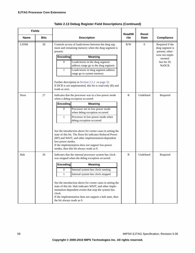
EJTAG Processor Core Extensions
58 MIPS® EJTAG Specification, Revision 5.06
Copyright © 2000-2010 MIPS Technologies Inc. All rights reserved.
LSNM 28 Controls access of loads/stores between the dseg seg-ment and remaining memory when the dseg segment ispresent:
Further description in Section 2.2.2 on page 32.If DCR is not implemented, this bit is read-only (R) andreads as zero.
R/W 0 Required if thedseg segment ispresent; other-wise not imple-
mented.See bit 29,NoDCR.
Doze 27 Indicates that the processor was in a low-power modewhen a debug exception occurred:
See the introduction above for corner cases in setting thestate of this bit. The Doze bit indicates Reduced Power(RP) and WAIT, and other implementation-dependentlow-power modes.If the implementation does not support low-powermodes, then this bit always reads as 0.
R Undefined Required
Halt 26 Indicates that the internal processor system bus clockwas stopped when the debug exception occurred:
See the introduction above for corner cases in setting thestate of this bit. Halt indicates WAIT, and other imple-mentation-dependent events that stop the system busclock.If the implementation does not support a halt state, thenthe bit always reads as 0.
R Undefined Required
Table 2.13 Debug Register Field Descriptions (Continued)
Fields
DescriptionRead/W
riteResetState ComplianceName Bits
Encoding Meaning
0 Loads/stores in the dseg segmentaddress range go to the dseg segment
1 Loads/stores in dseg segment addressrange go to system memory
Encoding Meaning
0 Processor not in low-power modewhen debug exception occurred
1 Processor in low-power mode whendebug exception occurred
Encoding Meaning
0 Internal system bus clock running
1 Internal system bus clock stopped
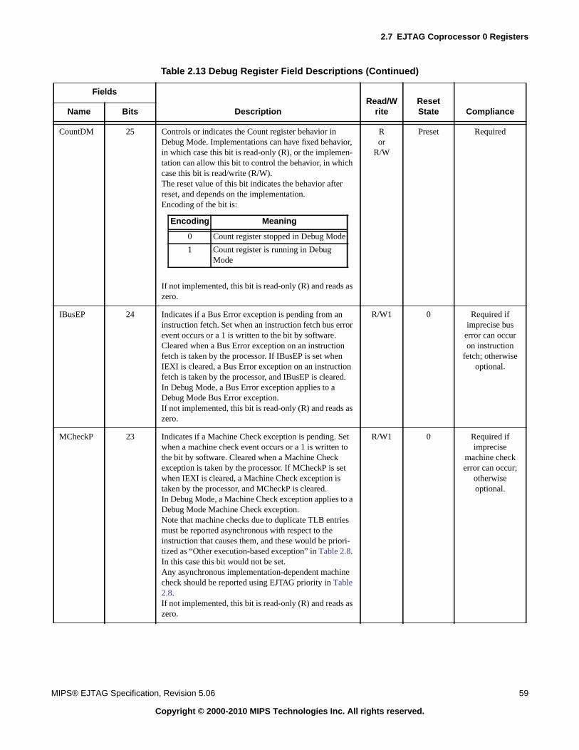
2.7 EJTAG Coprocessor 0 Registers
MIPS® EJTAG Specification, Revision 5.06 59
Copyright © 2000-2010 MIPS Technologies Inc. All rights reserved.
CountDM 25 Controls or indicates the Count register behavior inDebug Mode. Implementations can have fixed behavior,in which case this bit is read-only (R), or the implemen-tation can allow this bit to control the behavior, in whichcase this bit is read/write (R/W).The reset value of this bit indicates the behavior afterreset, and depends on the implementation.Encoding of the bit is:
If not implemented, this bit is read-only (R) and reads aszero.
Ror
R/W
Preset Required
IBusEP 24 Indicates if a Bus Error exception is pending from aninstruction fetch. Set when an instruction fetch bus errorevent occurs or a 1 is written to the bit by software.Cleared when a Bus Error exception on an instructionfetch is taken by the processor. If IBusEP is set whenIEXI is cleared, a Bus Error exception on an instructionfetch is taken by the processor, and IBusEP is cleared.In Debug Mode, a Bus Error exception applies to aDebug Mode Bus Error exception.If not implemented, this bit is read-only (R) and reads aszero.
R/W1 0 Required ifimprecise bus
error can occuron instruction
fetch; otherwiseoptional.
MCheckP 23 Indicates if a Machine Check exception is pending. Setwhen a machine check event occurs or a 1 is written tothe bit by software. Cleared when a Machine Checkexception is taken by the processor. If MCheckP is setwhen IEXI is cleared, a Machine Check exception istaken by the processor, and MCheckP is cleared.In Debug Mode, a Machine Check exception applies to aDebug Mode Machine Check exception.Note that machine checks due to duplicate TLB entriesmust be reported asynchronous with respect to theinstruction that causes them, and these would be priori-tized as “Other execution-based exception” in Table 2.8.In this case this bit would not be set.Any asynchronous implementation-dependent machinecheck should be reported using EJTAG priority in Table2.8.If not implemented, this bit is read-only (R) and reads aszero.
R/W1 0 Required ifimprecise
machine checkerror can occur;
otherwiseoptional.
Table 2.13 Debug Register Field Descriptions (Continued)
Fields
DescriptionRead/W
riteResetState ComplianceName Bits
Encoding Meaning
0 Count register stopped in Debug Mode
1 Count register is running in DebugMode
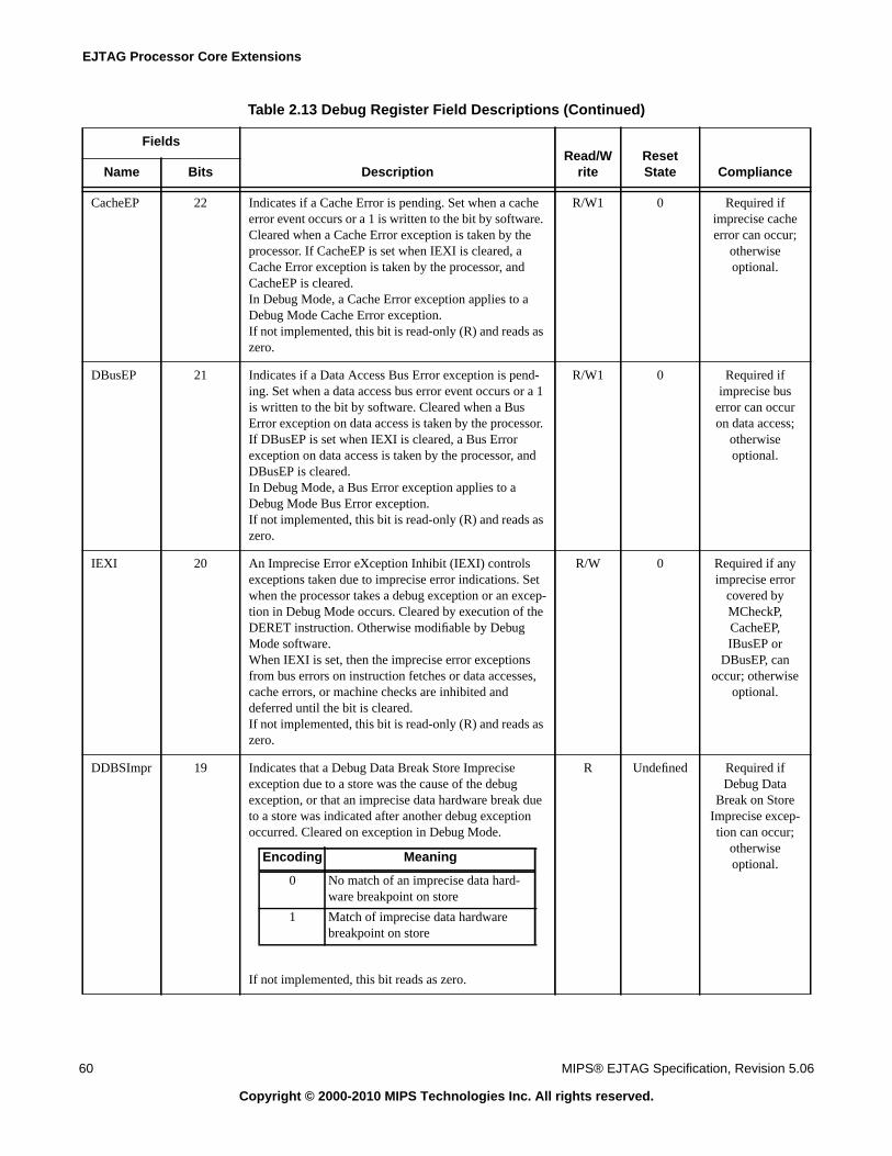
EJTAG Processor Core Extensions
60 MIPS® EJTAG Specification, Revision 5.06
Copyright © 2000-2010 MIPS Technologies Inc. All rights reserved.
CacheEP 22 Indicates if a Cache Error is pending. Set when a cacheerror event occurs or a 1 is written to the bit by software.Cleared when a Cache Error exception is taken by theprocessor. If CacheEP is set when IEXI is cleared, aCache Error exception is taken by the processor, andCacheEP is cleared.In Debug Mode, a Cache Error exception applies to aDebug Mode Cache Error exception.If not implemented, this bit is read-only (R) and reads aszero.
R/W1 0 Required ifimprecise cacheerror can occur;
otherwiseoptional.
DBusEP 21 Indicates if a Data Access Bus Error exception is pend-ing. Set when a data access bus error event occurs or a 1is written to the bit by software. Cleared when a BusError exception on data access is taken by the processor.If DBusEP is set when IEXI is cleared, a Bus Errorexception on data access is taken by the processor, andDBusEP is cleared.In Debug Mode, a Bus Error exception applies to aDebug Mode Bus Error exception.If not implemented, this bit is read-only (R) and reads aszero.
R/W1 0 Required ifimprecise bus
error can occuron data access;
otherwiseoptional.
IEXI 20 An Imprecise Error eXception Inhibit (IEXI) controlsexceptions taken due to imprecise error indications. Setwhen the processor takes a debug exception or an excep-tion in Debug Mode occurs. Cleared by execution of theDERET instruction. Otherwise modifiable by DebugMode software.When IEXI is set, then the imprecise error exceptionsfrom bus errors on instruction fetches or data accesses,cache errors, or machine checks are inhibited anddeferred until the bit is cleared.If not implemented, this bit is read-only (R) and reads aszero.
R/W 0 Required if anyimprecise error
covered byMCheckP,CacheEP,IBusEP or
DBusEP, canoccur; otherwise
optional.
DDBSImpr 19 Indicates that a Debug Data Break Store Impreciseexception due to a store was the cause of the debugexception, or that an imprecise data hardware break dueto a store was indicated after another debug exceptionoccurred. Cleared on exception in Debug Mode.
If not implemented, this bit reads as zero.
R Undefined Required ifDebug Data
Break on StoreImprecise excep-tion can occur;
otherwiseoptional.
Table 2.13 Debug Register Field Descriptions (Continued)
Fields
DescriptionRead/W
riteResetState ComplianceName Bits
Encoding Meaning
0 No match of an imprecise data hard-ware breakpoint on store
1 Match of imprecise data hardwarebreakpoint on store
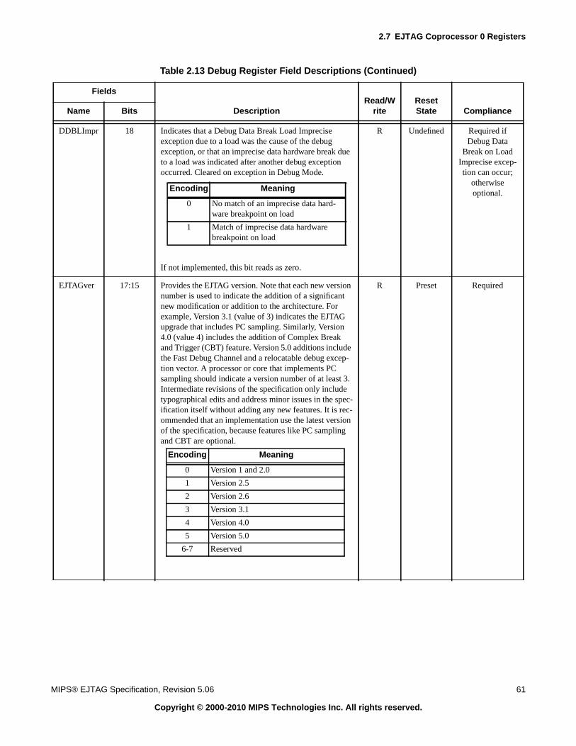
2.7 EJTAG Coprocessor 0 Registers
MIPS® EJTAG Specification, Revision 5.06 61
Copyright © 2000-2010 MIPS Technologies Inc. All rights reserved.
DDBLImpr 18 Indicates that a Debug Data Break Load Impreciseexception due to a load was the cause of the debugexception, or that an imprecise data hardware break dueto a load was indicated after another debug exceptionoccurred. Cleared on exception in Debug Mode.
If not implemented, this bit reads as zero.
R Undefined Required ifDebug Data
Break on LoadImprecise excep-tion can occur;
otherwiseoptional.
EJTAGver 17:15 Provides the EJTAG version. Note that each new versionnumber is used to indicate the addition of a significantnew modification or addition to the architecture. Forexample, Version 3.1 (value of 3) indicates the EJTAGupgrade that includes PC sampling. Similarly, Version4.0 (value 4) includes the addition of Complex Breakand Trigger (CBT) feature. Version 5.0 additions includethe Fast Debug Channel and a relocatable debug excep-tion vector. A processor or core that implements PCsampling should indicate a version number of at least 3.Intermediate revisions of the specification only includetypographical edits and address minor issues in the spec-ification itself without adding any new features. It is rec-ommended that an implementation use the latest versionof the specification, because features like PC samplingand CBT are optional.
R Preset Required
Table 2.13 Debug Register Field Descriptions (Continued)
Fields
DescriptionRead/W
riteResetState ComplianceName Bits
Encoding Meaning
0 No match of an imprecise data hard-ware breakpoint on load
1 Match of imprecise data hardwarebreakpoint on load
Encoding Meaning
0 Version 1 and 2.0
1 Version 2.5
2 Version 2.6
3 Version 3.1
4 Version 4.0
5 Version 5.0
6-7 Reserved
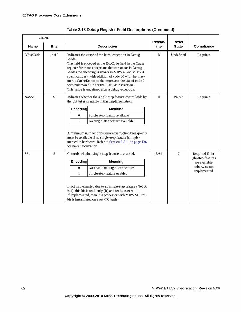
EJTAG Processor Core Extensions
62 MIPS® EJTAG Specification, Revision 5.06
Copyright © 2000-2010 MIPS Technologies Inc. All rights reserved.
DExcCode 14:10 Indicates the cause of the latest exception in DebugMode.The field is encoded as the ExcCode field in the Causeregister for those exceptions that can occur in DebugMode (the encoding is shown in MIPS32 and MIPS64specifications), with addition of code 30 with the mne-monic CacheErr for cache errors and the use of code 9with mnemonic Bp for the SDBBP instruction.This value is undefined after a debug exception.
R Undefined Required
NoSSt 9 Indicates whether the single-step feature controllable bythe SSt bit is available in this implementation:
A minimum number of hardware instruction breakpointsmust be available if no single-step feature is imple-mented in hardware. Refer to Section 5.8.1 on page 136for more information.
R Preset Required
SSt 8 Controls whether single-step feature is enabled:
If not implemented due to no single-step feature (NoSStis 1), this bit is read-only (R) and reads as zero.If implemented, then in a processor with MIPS MT, thisbit is instantiated on a per-TC basis.
R/W 0 Required if sin-gle-step features
are available;otherwise notimplemented.
Table 2.13 Debug Register Field Descriptions (Continued)
Fields
DescriptionRead/W
riteResetState ComplianceName Bits
Encoding Meaning
0 Single-step feature available
1 No single-step feature available
Encoding Meaning
0 No enable of single-step feature
1 Single-step feature enabled
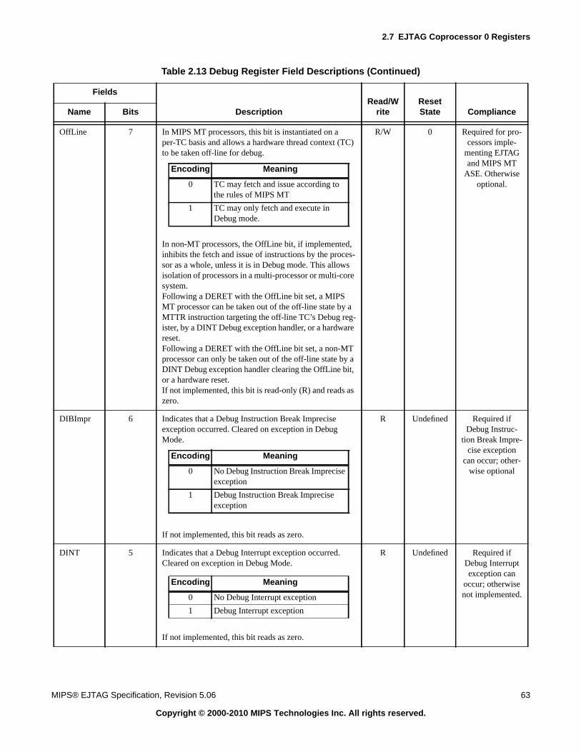
2.7 EJTAG Coprocessor 0 Registers
MIPS® EJTAG Specification, Revision 5.06 63
Copyright © 2000-2010 MIPS Technologies Inc. All rights reserved.
OffLine 7 In MIPS MT processors, this bit is instantiated on aper-TC basis and allows a hardware thread context (TC)to be taken off-line for debug.
In non-MT processors, the OffLine bit, if implemented,inhibits the fetch and issue of instructions by the proces-sor as a whole, unless it is in Debug mode. This allowsisolation of processors in a multi-processor or multi-coresystem.Following a DERET with the OffLine bit set, a MIPSMT processor can be taken out of the off-line state by aMTTR instruction targeting the off-line TC’s Debug reg-ister, by a DINT Debug exception handler, or a hardwarereset.Following a DERET with the OffLine bit set, a non-MTprocessor can only be taken out of the off-line state by aDINT Debug exception handler clearing the OffLine bit,or a hardware reset.If not implemented, this bit is read-only (R) and reads aszero.
R/W 0 Required for pro-cessors imple-
menting EJTAGand MIPS MT
ASE. Otherwiseoptional.
DIBImpr 6 Indicates that a Debug Instruction Break Impreciseexception occurred. Cleared on exception in DebugMode.
If not implemented, this bit reads as zero.
R Undefined Required ifDebug Instruc-
tion Break Impre-cise exception
can occur; other-wise optional
DINT 5 Indicates that a Debug Interrupt exception occurred.Cleared on exception in Debug Mode.
If not implemented, this bit reads as zero.
R Undefined Required ifDebug Interruptexception can
occur; otherwisenot implemented.
Table 2.13 Debug Register Field Descriptions (Continued)
Fields
DescriptionRead/W
riteResetState ComplianceName Bits
Encoding Meaning
0 TC may fetch and issue according tothe rules of MIPS MT
1 TC may only fetch and execute inDebug mode.
Encoding Meaning
0 No Debug Instruction Break Impreciseexception
1 Debug Instruction Break Impreciseexception
Encoding Meaning
0 No Debug Interrupt exception
1 Debug Interrupt exception
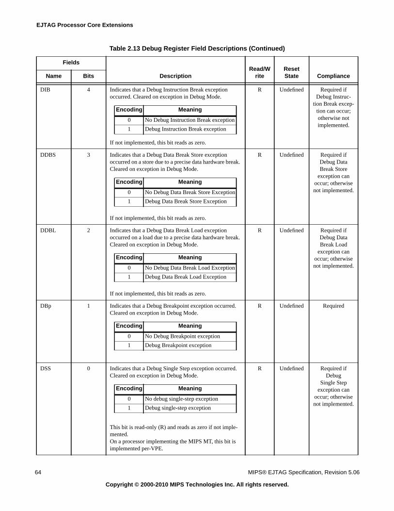
EJTAG Processor Core Extensions
64 MIPS® EJTAG Specification, Revision 5.06
Copyright © 2000-2010 MIPS Technologies Inc. All rights reserved.
DIB 4 Indicates that a Debug Instruction Break exceptionoccurred. Cleared on exception in Debug Mode.
If not implemented, this bit reads as zero.
R Undefined Required ifDebug Instruc-
tion Break excep-tion can occur;otherwise notimplemented.
DDBS 3 Indicates that a Debug Data Break Store exceptionoccurred on a store due to a precise data hardware break.Cleared on exception in Debug Mode.
If not implemented, this bit reads as zero.
R Undefined Required ifDebug DataBreak Store
exception canoccur; otherwisenot implemented.
DDBL 2 Indicates that a Debug Data Break Load exceptionoccurred on a load due to a precise data hardware break.Cleared on exception in Debug Mode.
If not implemented, this bit reads as zero.
R Undefined Required ifDebug DataBreak Load
exception canoccur; otherwisenot implemented.
DBp 1 Indicates that a Debug Breakpoint exception occurred.Cleared on exception in Debug Mode.
R Undefined Required
DSS 0 Indicates that a Debug Single Step exception occurred.Cleared on exception in Debug Mode.
This bit is read-only (R) and reads as zero if not imple-mented.On a processor implementing the MIPS MT, this bit isimplemented per-VPE.
R Undefined Required ifDebug
Single Stepexception can
occur; otherwisenot implemented.
Table 2.13 Debug Register Field Descriptions (Continued)
Fields
DescriptionRead/W
riteResetState ComplianceName Bits
Encoding Meaning
0 No Debug Instruction Break exception
1 Debug Instruction Break exception
Encoding Meaning
0 No Debug Data Break Store Exception
1 Debug Data Break Store Exception
Encoding Meaning
0 No Debug Data Break Load Exception
1 Debug Data Break Load Exception
Encoding Meaning
0 No Debug Breakpoint exception
1 Debug Breakpoint exception
Encoding Meaning
0 No debug single-step exception
1 Debug single-step exception
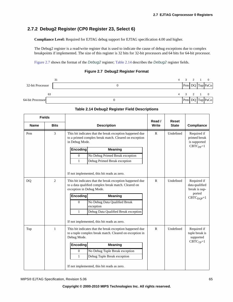
2.7 EJTAG Coprocessor 0 Registers
MIPS® EJTAG Specification, Revision 5.06 65
Copyright © 2000-2010 MIPS Technologies Inc. All rights reserved.
2.7.2 Debug2 Register (CP0 Register 23, Select 6)
Compliance Level: Required for EJTAG debug support for EJTAG specification 4.00 and higher.
The Debug2 register is a read/write register that is used to indicate the cause of debug exceptions due to complexbreakpoints if implemented. The size of this register is 32 bits for 32-bit processors and 64 bits for 64-bit processor.
Figure 2.7 shows the format of the Debug2 register; Table 2.14 describes the Debug2 register fields.
Figure 2.7 Debug2 Register Format
31 4 3 2 1 0
32-bit Processor 0 Prm DQ Tup PaCo
63 4 3 2 1 0
64-bit Processor 0 Prm DQ Tup PaCo
Table 2.14 Debug2 Register Field Descriptions
Fields
DescriptionRead /Write
ResetState ComplianceName Bits
Prm 3 This bit indicates that the break exception happened dueto a primed complex break match. Cleared on exceptionin Debug Mode.
If not implemented, this bit reads as zero.
R Undefined Required ifprimed breakis supportedCBTCPP=1
DQ 2 This bit indicates that the break exception happened dueto a data qualified complex break match. Cleared onexception in Debug Mode.
If not implemented, this bit reads as zero.
R Undefined Required ifdata qualifiedbreak is sup-
portedCBTCDQP=1
Tup 1 This bit indicates that the break exception happened dueto a tuple complex break match. Cleared on exception inDebug Mode.
If not implemented, this bit reads as zero.
R Undefined Required iftuple break is
supportedCBTCTP=1
Encoding Meaning
0 No Debug Primed Break exception
1 Debug Primed Break exception
Encoding Meaning
0 No Debug Data Qualified Breakexception
1 Debug Data Qualified Break exception
Encoding Meaning
0 No Debug Tuple Break exception
1 Debug Tuple Break exception
EJTAG Processor Core Extensions
66 MIPS® EJTAG Specification, Revision 5.06
Copyright © 2000-2010 MIPS Technologies Inc. All rights reserved.
2.7.3 Debug Exception Program Counter Register (CP0 Register 24, Select 0)
Compliance Level: Required for EJTAG debug support.
The Debug Exception Program Counter (DEPC) register is a read/write register that contains the address at whichprocessing resumes after the exception has been serviced. The size of this register is 32 bits for 32-bit processors and64 bits for 64-bit processors, even with only 32-bit virtual addressing enabled. All bits of the DEPC register are sig-nificant and writable. A DMFC0 from the DEPC register returns the full 64-bit DEPC on 64-bit processors.
Hardware updates this register on debug exceptions and exceptions in Debug Mode.
For precise debug exceptions and precise exceptions in Debug Mode, the DEPC register contains either:
• the virtual address of the instruction that was the direct cause of the exception, or
• the virtual address of the immediately preceding branch or jump instruction, when the exception-causing instruc-tion is in a branch delay slot, and the Debug Branch Delay (BDB) bit in the Debug register is set.
For imprecise debug exceptions and imprecise exceptions in Debug Mode, the DEPC register contains the address atwhich execution is resumed when returning to Non-Debug Mode.
On debug exceptions and exceptions in debug mode, bit 0 of DEPC is set by hardware to indicate the ISA mode to beused when execution restarts. Processors without MIPS16 set bit 0 to zero.
Figure 2.8 shows the format of the DEPC register; Table 2.15 describes the DEPC register field.
PaCo 0 This bit indicates that the break exception happenedwhen a pass counter in the complex break unit reached azero count (this overrides other settings on the break-point, such as data qualifier or prime condition). Clearedon exception in Debug Mode.
If not implemented, this bit reads as zero.
R Undefined Required ifpass counteris supportedCBTCPCP=1
0 MSB:4 Must be written as zeros return zeros on reads. 0 0 Reserved
Table 2.14 Debug2 Register Field Descriptions (Continued)
Fields
DescriptionRead /Write
ResetState ComplianceName Bits
Encoding Meaning
0 No Debug Instruction, Data, or TupleBreak on pass counter exception
1 Debug Instruction, Data, or TupleBreak on pass counter exception
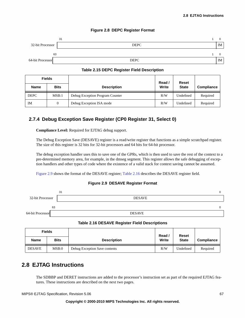
2.8 EJTAG Instructions
MIPS® EJTAG Specification, Revision 5.06 67
Copyright © 2000-2010 MIPS Technologies Inc. All rights reserved.
Figure 2.8 DEPC Register Format
2.7.4 Debug Exception Save Register (CP0 Register 31, Select 0)
Compliance Level: Required for EJTAG debug support.
The Debug Exception Save (DESAVE) register is a read/write register that functions as a simple scratchpad register.The size of this register is 32 bits for 32-bit processors and 64 bits for 64-bit processor.
The debug exception handler uses this to save one of the GPRs, which is then used to save the rest of the context to apre-determined memory area, for example, in the dmseg segment. This register allows the safe debugging of excep-tion handlers and other types of code where the existence of a valid stack for context saving cannot be assumed.
Figure 2.9 shows the format of the DESAVE register; Table 2.16 describes the DESAVE register field.
Figure 2.9 DESAVE Register Format
2.8 EJTAG Instructions
The SDBBP and DERET instructions are added to the processor’s instruction set as part of the required EJTAG fea-tures. These instructions are described on the next two pages.
31 1 0
32-bit Processor DEPC IM
63 1 0
64-bit Processor DEPC IM
Table 2.15 DEPC Register Field Description
Fields
DescriptionRead /Write
ResetState ComplianceName Bits
DEPC MSB:1 Debug Exception Program Counter R/W Undefined Required
IM 0 Debug Exception ISA mode R/W Undefined Required
31 0
32-bit Processor DESAVE
63 0
64-bit Processor DESAVE
Table 2.16 DESAVE Register Field Descriptions
Fields
DescriptionRead /Write
ResetState ComplianceName Bits
DESAVE MSB:0 Debug Exception Save contents R/W Undefined Required
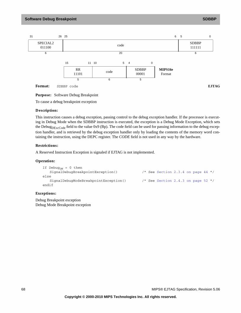
Software Debug Breakpoint SDBBP
68 MIPS® EJTAG Specification, Revision 5.06
Copyright © 2000-2010 MIPS Technologies Inc. All rights reserved.
Format: SDBBP code EJTAG
Purpose: Software Debug Breakpoint
To cause a debug breakpoint exception
Description:
This instruction causes a debug exception, passing control to the debug exception handler. If the processor is execut-ing in Debug Mode when the SDBBP instruction is executed, the exception is a Debug Mode Exception, which setsthe DebugDExcCode field to the value 0x9 (Bp). The code field can be used for passing information to the debug excep-tion handler, and is retrieved by the debug exception handler only by loading the contents of the memory word con-taining the instruction, using the DEPC register. The CODE field is not used in any way by the hardware.
Restrictions:
A Reserved Instruction Exception is signaled if EJTAG is not implemented.
Operation:
If DebugDM = 0 thenSignalDebugBreakpointException() /* See Section 2.3.4 on page 44 */
elseSignalDebugModeBreakpointException() /* See Section 2.4.3 on page 52 */
endif
Exceptions:
Debug Breakpoint exceptionDebug Mode Breakpoint exception
31 26 25 6 5 0
SPECIAL2011100
codeSDBBP111111
6 20 6
15 11 10 5 4 0
RR11101
codeSDBBP00001
MIPS16eFormat
5 6 5
Software Debug Breakpoint SDBBP
MIPS® EJTAG Specification, Revision 5.06 69
Copyright © 2000-2010 MIPS Technologies Inc. All rights reserved.
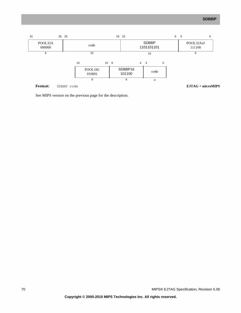
SDBBP
70 MIPS® EJTAG Specification, Revision 5.06
Copyright © 2000-2010 MIPS Technologies Inc. All rights reserved.
Format: SDBBP code EJTAG + microMIPS
See MIPS version on the previous page for the description.
31 26 25 16 15 6 5 0
POOL32A000000
codeSDBBP
1101101101POOL32Axf
111100
6 10 10 6
15 10 9 4 3 0
POOL16C010001
SDBBP16101100
code
6 6 4
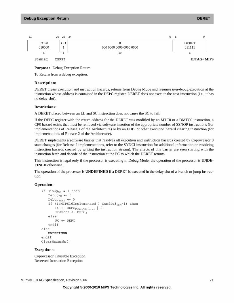
Debug Exception Return DERET
MIPS® EJTAG Specification, Revision 5.06 71
Copyright © 2000-2010 MIPS Technologies Inc. All rights reserved.
Format: DERET EJTAG+ MIPS
Purpose: Debug Exception Return
To Return from a debug exception.
Description:
DERET clears execution and instruction hazards, returns from Debug Mode and resumes non-debug execution at theinstruction whose address is contained in the DEPC register. DERET does not execute the next instruction (i.e., it hasno delay slot).
Restrictions:
A DERET placed between an LL and SC instruction does not cause the SC to fail.
If the DEPC register with the return address for the DERET was modified by an MTC0 or a DMTC0 instruction, aCP0 hazard exists that must be removed via software insertion of the appropriate number of SSNOP instructions (forimplementations of Release 1 of the Architecture) or by an EHB, or other execution hazard clearing instruction (forimplementations of Release 2 of the Architecture).
DERET implements a software barrier that resolves all execution and instruction hazards created by Coprocessor 0state changes (for Release 2 implementations, refer to the SYNCI instruction for additional information on resolvinginstruction hazards created by writing the instruction stream). The effects of this barrier are seen starting with theinstruction fetch and decode of the instruction at the PC to which the DERET returns.
This instruction is legal only if the processor is executing in Debug Mode, the operation of the processor is UNDE-FINED otherwise.
The operation of the processor is UNDEFINED if a DERET is executed in the delay slot of a branch or jump instruc-tion.
Operation:
if DebugDM = 1 thenDebugDM ← 0DebugIEXI ← 0if (IsMIPS16Implemented()|Config3ISA>1) then
PC ← DEPCPCWIDTH-1..1 || 0ISAMode ← DEPC0
elsePC ← DEPC
endifelse
UNDEFINEDendifClearHazards()
Exceptions:
Coprocessor Unusable ExceptionReserved Instruction Exception
31 26 25 24 6 5 0
COP0010000
CO1
0000 0000 0000 0000 0000
DERET011111
6 1 19 6
Debug Exception Return DERET
72 MIPS® EJTAG Specification, Revision 5.06
Copyright © 2000-2010 MIPS Technologies Inc. All rights reserved.
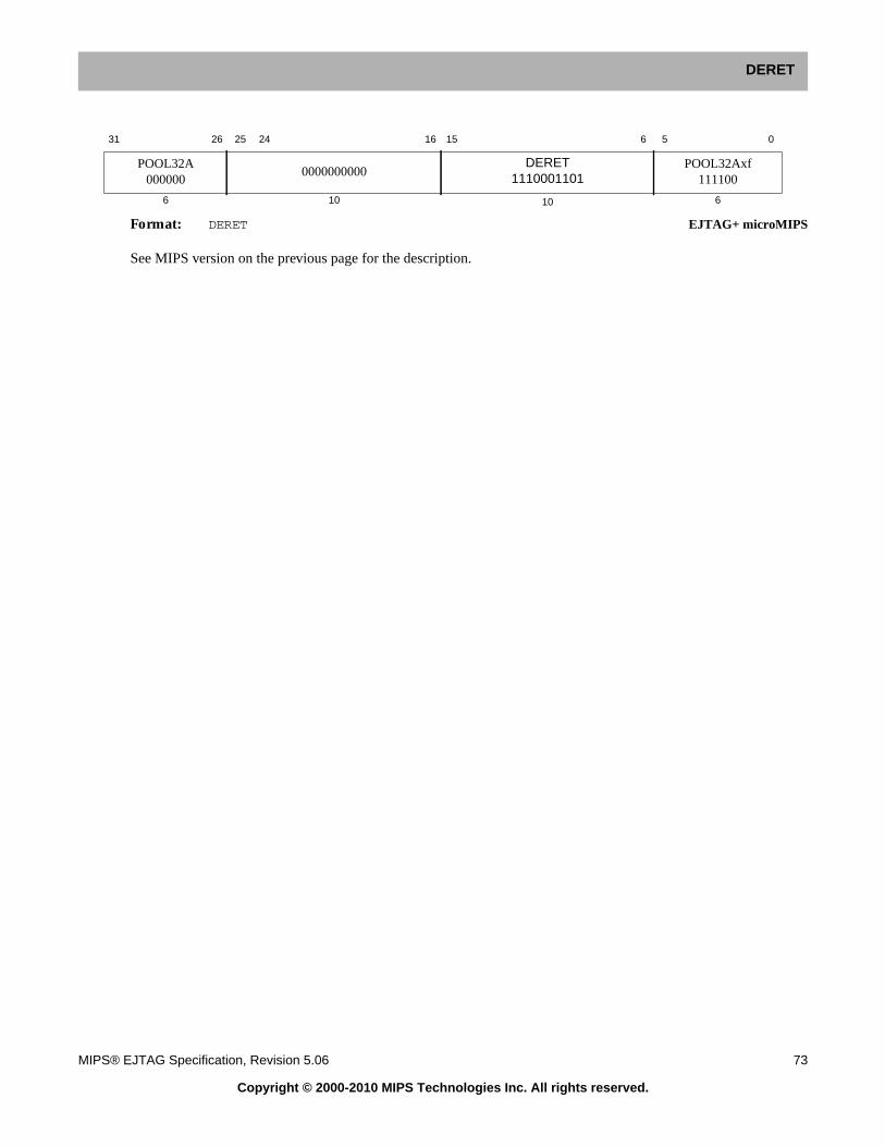
DERET
MIPS® EJTAG Specification, Revision 5.06 73
Copyright © 2000-2010 MIPS Technologies Inc. All rights reserved.
Format: DERET EJTAG+ microMIPS
See MIPS version on the previous page for the description.
31 26 25 24 16 15 6 5 0
POOL32A000000
0000000000DERET
1110001101POOL32Axf
111100
6 10 10 6

DERET
74 MIPS® EJTAG Specification, Revision 5.06
Copyright © 2000-2010 MIPS Technologies Inc. All rights reserved.
Chapter 3
MIPS® EJTAG Specification, Revision 5.06 75
Copyright © 2000-2010 MIPS Technologies Inc. All rights reserved.
Debug Control Register
Compliance Level: Optional, but requires EJTAG processor core extensions. If this register is not implemented thenother features that depend on bits in this register behave as if these bits are present and have the reset value.
The Debug Control Register (DCR) controls and provides information about debug issues. The width of the register is32 bits for 32-bit processors, and 64 bits for 64-bit processors. The DCR is located in the drseg segment at offset0x0000.
The Debug Control Register (DCR) provides the following key features:
• Interrupt and NMI control when in Non-Debug Mode
• NMI pending indication
• Availability indicator of instruction and data hardware breakpoints
• Availability and control of of the PC sample feature and its sample period
• Availability of the Fast Debug Channel (FDC) feature
For EJTAG features, there are no differences between a reset and a soft reset occurring to the processor; they behaveidentically in both Debug Mode and Non-Debug Mode. Therefore all references to reset in this chapter refer to bothreset (hard reset) and soft reset.
The DataBrk and InstBrk bits within the DCR indicate the types of hardware breakpoints implemented. Debug soft-ware is expected to read hardware breakpoint registers for additional information on the number of implementedbreakpoints. Refer to Chapter 5, “Hardware Breakpoints” on page 111 for descriptions of the hardware breakpointregisters.
Hardware and software interrupts can be disabled in Non-Debug Mode using the DCR’s IntE bit. This bit is a globalinterrupt enable used along with several other interrupt enables that enable specific mechanisms. The NMI interruptcan be disabled in Non-Debug Mode using the DCR’s NMIE bit; a pending NMI is indicated through the NMIpendbit. Pending interrupts are indicated in the Cause register, and pending NMIs are indicated in the DCR register NMI-pend bit, even when disabled. Hardware and software interrupts and NMIs are always disabled in Debug Mode. SeeSection 2.5 on page 53 for more information.
The optional SRstE bit allows masking of soft resets. A soft reset can be applied to the system based on differentevents, referred to as sources. It is implementation-dependent which soft reset sources in a system can be masked bythe SRstE bit. Soft reset masking can be applied to a soft reset source only if that source can be efficiently masked inthe system. The result is no reset at all for any part of the system, if masked. If only a partial soft reset is possible, thenthat soft reset source is not to be masked, because a “half” soft reset might cause the system to fail or hang withoutwarning. There is no automatic indication of whether the SRstE bit is effective, so the user must consult system docu-mentation.
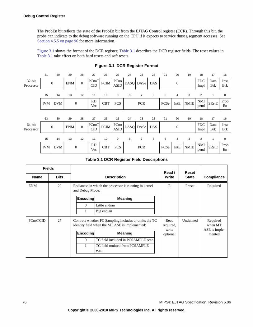
Debug Control Register
76 MIPS® EJTAG Specification, Revision 5.06
Copyright © 2000-2010 MIPS Technologies Inc. All rights reserved.
The ProbEn bit reflects the state of the ProbEn bit from the EJTAG Control register (ECR). Through this bit, theprobe can indicate to the debug software running on the CPU if it expects to service dmseg segment accesses. SeeSection 4.5.5 on page 96 for more information.
Figure 3.1 shows the format of the DCR register; Table 3.1 describes the DCR register fields. The reset values inTable 3.1 take effect on both hard resets and soft resets.
Figure 3.1 DCR Register Format
31 30 29 28 27 26 25 24 23 22 21 20 19 18 17 16
32-bitProcessor
0 ENM 0PCnoT
CIDPCIM
PCnoASID
DASQ DASe DAS 0FDCImpl
DataBrk
InstBrk
15 14 13 12 11 10 9 8 7 6 5 4 3 2 1 0
IVM DVM 0RDVec
CBT PCS PCR PCSe IntE NMIENMIpend
SRstEProbEn
63 30 29 28 27 26 25 24 23 22 21 20 19 18 17 16
64-bitProcessor
0 ENM 0PCnoT
CIDPCIM
PCnoASID
DASQ DASe DAS 0FDCImpl
DataBrk
InstBrk
15 14 13 12 11 10 9 8 7 6 5 4 3 2 1 0
IVM DVM 0RDVec
CBT PCS PCR PCSe IntE NMIENMIpend
SRstEProbEn
Table 3.1 DCR Register Field Descriptions
Fields
DescriptionRead /Write
ResetState ComplianceName Bits
ENM 29 Endianess in which the processor is running in kerneland Debug Mode:
R Preset Required
PCnoTCID 27 Controls whether PC Sampling includes or omits the TCidentity field when the MT ASE is implemented:
Readrequired,
writeoptional
Undefined Requiredwhen MT
ASE is imple-mented
Encoding Meaning
0 Little endian
1 Big endian
Encoding Meaning
0 TC field included in PCSAMPLE scan
1 TC field omitted from PCSAMPLEscan
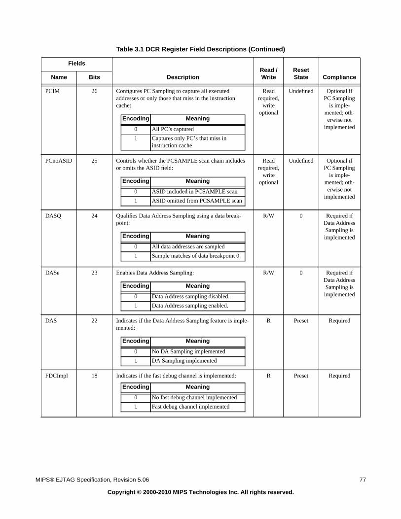
MIPS® EJTAG Specification, Revision 5.06 77
Copyright © 2000-2010 MIPS Technologies Inc. All rights reserved.
PCIM 26 Configures PC Sampling to capture all executedaddresses or only those that miss in the instructioncache:
Readrequired,
writeoptional
Undefined Optional ifPC Sampling
is imple-mented; oth-erwise not
implemented
PCnoASID 25 Controls whether the PCSAMPLE scan chain includesor omits the ASID field:
Readrequired,
writeoptional
Undefined Optional ifPC Sampling
is imple-mented; oth-erwise not
implemented
DASQ 24 Qualifies Data Address Sampling using a data break-point:
R/W 0 Required ifData AddressSampling isimplemented
DASe 23 Enables Data Address Sampling: R/W 0 Required ifData AddressSampling isimplemented
DAS 22 Indicates if the Data Address Sampling feature is imple-mented:
R Preset Required
FDCImpl 18 Indicates if the fast debug channel is implemented: R Preset Required
Table 3.1 DCR Register Field Descriptions (Continued)
Fields
DescriptionRead /Write
ResetState ComplianceName Bits
Encoding Meaning
0 All PC’s captured
1 Captures only PC’s that miss ininstruction cache
Encoding Meaning
0 ASID included in PCSAMPLE scan
1 ASID omitted from PCSAMPLE scan
Encoding Meaning
0 All data addresses are sampled
1 Sample matches of data breakpoint 0
Encoding Meaning
0 Data Address sampling disabled.
1 Data Address sampling enabled.
Encoding Meaning
0 No DA Sampling implemented
1 DA Sampling implemented
Encoding Meaning
0 No fast debug channel implemented
1 Fast debug channel implemented
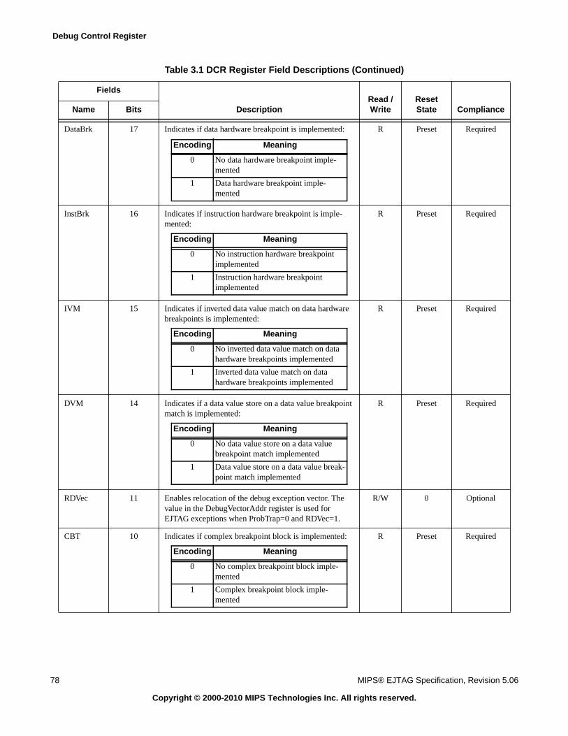
Debug Control Register
78 MIPS® EJTAG Specification, Revision 5.06
Copyright © 2000-2010 MIPS Technologies Inc. All rights reserved.
DataBrk 17 Indicates if data hardware breakpoint is implemented: R Preset Required
InstBrk 16 Indicates if instruction hardware breakpoint is imple-mented:
R Preset Required
IVM 15 Indicates if inverted data value match on data hardwarebreakpoints is implemented:
R Preset Required
DVM 14 Indicates if a data value store on a data value breakpointmatch is implemented:
R Preset Required
RDVec 11 Enables relocation of the debug exception vector. Thevalue in the DebugVectorAddr register is used forEJTAG exceptions when ProbTrap=0 and RDVec=1.
R/W 0 Optional
CBT 10 Indicates if complex breakpoint block is implemented: R Preset Required
Table 3.1 DCR Register Field Descriptions (Continued)
Fields
DescriptionRead /Write
ResetState ComplianceName Bits
Encoding Meaning
0 No data hardware breakpoint imple-mented
1 Data hardware breakpoint imple-mented
Encoding Meaning
0 No instruction hardware breakpointimplemented
1 Instruction hardware breakpointimplemented
Encoding Meaning
0 No inverted data value match on datahardware breakpoints implemented
1 Inverted data value match on datahardware breakpoints implemented
Encoding Meaning
0 No data value store on a data valuebreakpoint match implemented
1 Data value store on a data value break-point match implemented
Encoding Meaning
0 No complex breakpoint block imple-mented
1 Complex breakpoint block imple-mented
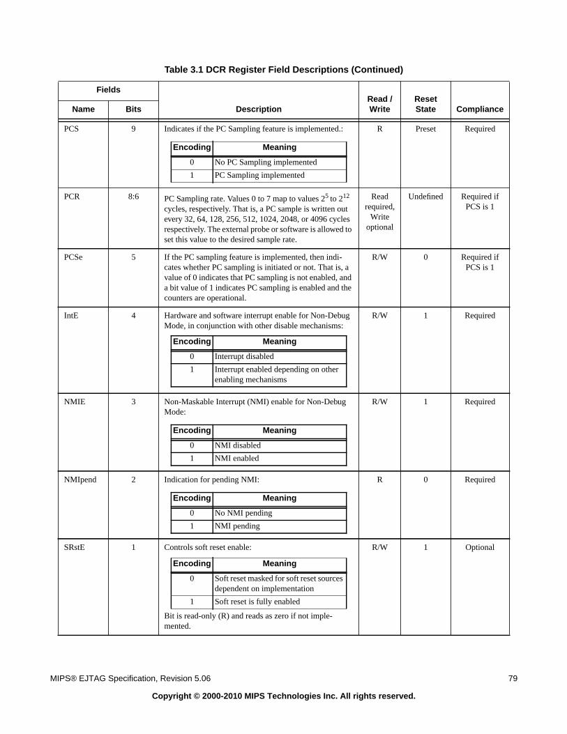
MIPS® EJTAG Specification, Revision 5.06 79
Copyright © 2000-2010 MIPS Technologies Inc. All rights reserved.
PCS 9 Indicates if the PC Sampling feature is implemented.: R Preset Required
PCR 8:6 PC Sampling rate. Values 0 to 7 map to values 25 to 212
cycles, respectively. That is, a PC sample is written outevery 32, 64, 128, 256, 512, 1024, 2048, or 4096 cyclesrespectively. The external probe or software is allowed toset this value to the desired sample rate.
Readrequired,
Writeoptional
Undefined Required ifPCS is 1
PCSe 5 If the PC sampling feature is implemented, then indi-cates whether PC sampling is initiated or not. That is, avalue of 0 indicates that PC sampling is not enabled, anda bit value of 1 indicates PC sampling is enabled and thecounters are operational.
R/W 0 Required ifPCS is 1
IntE 4 Hardware and software interrupt enable for Non-DebugMode, in conjunction with other disable mechanisms:
R/W 1 Required
NMIE 3 Non-Maskable Interrupt (NMI) enable for Non-DebugMode:
R/W 1 Required
NMIpend 2 Indication for pending NMI: R 0 Required
SRstE 1 Controls soft reset enable:
Bit is read-only (R) and reads as zero if not imple-mented.
R/W 1 Optional
Table 3.1 DCR Register Field Descriptions (Continued)
Fields
DescriptionRead /Write
ResetState ComplianceName Bits
Encoding Meaning
0 No PC Sampling implemented
1 PC Sampling implemented
Encoding Meaning
0 Interrupt disabled
1 Interrupt enabled depending on otherenabling mechanisms
Encoding Meaning
0 NMI disabled
1 NMI enabled
Encoding Meaning
0 No NMI pending
1 NMI pending
Encoding Meaning
0 Soft reset masked for soft reset sourcesdependent on implementation
1 Soft reset is fully enabled
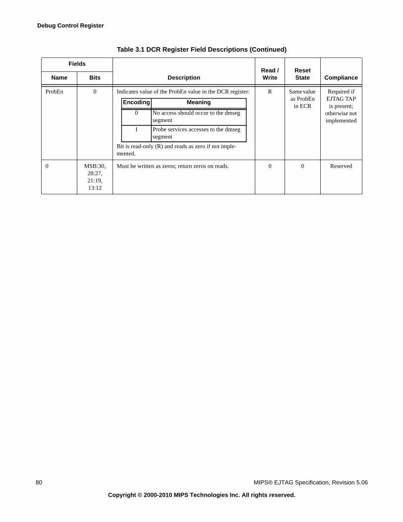
Debug Control Register
80 MIPS® EJTAG Specification, Revision 5.06
Copyright © 2000-2010 MIPS Technologies Inc. All rights reserved.
ProbEn 0 Indicates value of the ProbEn value in the DCR register:
Bit is read-only (R) and reads as zero if not imple-mented.
R Same valueas ProbEn
in ECR
Required ifEJTAG TAPis present;
otherwise notimplemented
0 MSB:30,28:27,21:19,13:12
Must be written as zeros; return zeros on reads. 0 0 Reserved
Table 3.1 DCR Register Field Descriptions (Continued)
Fields
DescriptionRead /Write
ResetState ComplianceName Bits
Encoding Meaning
0 No access should occur to the dmsegsegment
1 Probe services accesses to the dmsegsegment
Chapter 4
MIPS® EJTAG Specification, Revision 5.06 81
Copyright © 2000-2010 MIPS Technologies Inc. All rights reserved.
EJTAG Test Access Port
This chapter describes the EJTAG features provided when the optional EJTAG Test Access Port (TAP) is included inthe implementation. The TAP is an optional part of EJTAG, but if it is implemented, the DCR must also be imple-mented, and all the features in the TAP described below are required, except for those features explicitly described asoptional.
This chapter contains the following sections:
• Section 4.1 “TAP Overview”
• Section 4.2 “TAP Signals”
• Section 4.3 “TAP Controller”
• Section 4.4 “Instruction Register and Special Instructions”
• Section 4.5 “TAP Data Registers”
• Section 4.6 “Examples of Use”
4.1 TAP Overview
The overall features of the EJTAG Test Access Port (TAP) are:
• Identification of device and EJTAG debug features accessed through the TAP
• dmseg segment memory “emulation” (mapping dmseg segment processor accesses into probe transactions)
• Reset handling allows debug exception immediately after reset
• Debug interrupt request from probe
• Low-power mode indications
• Implementation-dependent processor and peripheral reset
If the TAP is not implemented, other features depending on register values and indications from the TAP shouldbehave as if these register values and indications have the power-up and reset values.
Figure 4.1 shows an overview of the elements in the TAP.
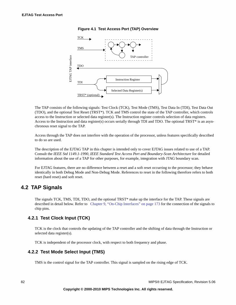
EJTAG Test Access Port
82 MIPS® EJTAG Specification, Revision 5.06
Copyright © 2000-2010 MIPS Technologies Inc. All rights reserved.
Figure 4.1 Test Access Port (TAP) Overview
The TAP consists of the following signals: Test Clock (TCK), Test Mode (TMS), Test Data In (TDI), Test Data Out(TDO), and the optional Test Reset (TRST*). TCK and TMS control the state of the TAP controller, which controlsaccess to the Instruction or selected data register(s). The Instruction register controls selection of data registers.Access to the Instruction and data register(s) occurs serially through TDI and TDO. The optional TRST* is an asyn-chronous reset signal to the TAP.
Access through the TAP does not interfere with the operation of the processor, unless features specifically describedto do so are used.
The description of the EJTAG TAP in this chapter is intended only to cover EJTAG issues related to use of a TAP.Consult the IEEE Std 1149.1-1990, IEEE Standard Test Access Port and Boundary-Scan Architecture for detailedinformation about the use of a TAP for other purposes, for example, integration with JTAG boundary scan.
For EJTAG features, there are no difference between a reset and a soft reset occurring to the processor; they behaveidentically in both Debug Mode and Non-Debug Mode. References to reset in the following therefore refers to bothreset (hard reset) and soft reset.
4.2 TAP Signals
The signals TCK, TMS, TDI, TDO, and the optional TRST* make up the interface for the TAP. These signals aredescribed in detail below. Refer to Chapter 9, “On-Chip Interfaces” on page 173 for the connection of the signals tochip pins.
4.2.1 Test Clock Input (TCK)
TCK is the clock that controls the updating of the TAP controller and the shifting of data through the Instruction orselected data register(s).
TCK is independent of the processor clock, with respect to both frequency and phase.
4.2.2 Test Mode Select Input (TMS)
TMS is the control signal for the TAP controller. This signal is sampled on the rising edge of TCK.
Instruction Register
Selected Data Register(s)
TDI
TDO
EJT
AG
TA
P in
terf
ace
TCK
TMS
TRST* (optional)
TAP controller
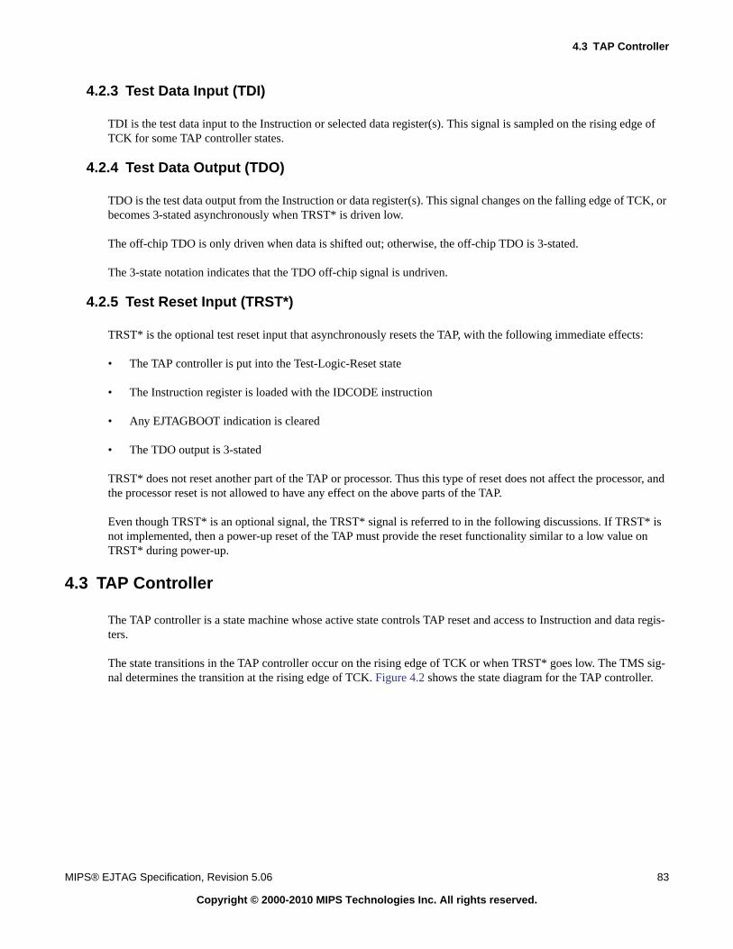
4.3 TAP Controller
MIPS® EJTAG Specification, Revision 5.06 83
Copyright © 2000-2010 MIPS Technologies Inc. All rights reserved.
4.2.3 Test Data Input (TDI)
TDI is the test data input to the Instruction or selected data register(s). This signal is sampled on the rising edge ofTCK for some TAP controller states.
4.2.4 Test Data Output (TDO)
TDO is the test data output from the Instruction or data register(s). This signal changes on the falling edge of TCK, orbecomes 3-stated asynchronously when TRST* is driven low.
The off-chip TDO is only driven when data is shifted out; otherwise, the off-chip TDO is 3-stated.
The 3-state notation indicates that the TDO off-chip signal is undriven.
4.2.5 Test Reset Input (TRST*)
TRST* is the optional test reset input that asynchronously resets the TAP, with the following immediate effects:
• The TAP controller is put into the Test-Logic-Reset state
• The Instruction register is loaded with the IDCODE instruction
• Any EJTAGBOOT indication is cleared
• The TDO output is 3-stated
TRST* does not reset another part of the TAP or processor. Thus this type of reset does not affect the processor, andthe processor reset is not allowed to have any effect on the above parts of the TAP.
Even though TRST* is an optional signal, the TRST* signal is referred to in the following discussions. If TRST* isnot implemented, then a power-up reset of the TAP must provide the reset functionality similar to a low value onTRST* during power-up.
4.3 TAP Controller
The TAP controller is a state machine whose active state controls TAP reset and access to Instruction and data regis-ters.
The state transitions in the TAP controller occur on the rising edge of TCK or when TRST* goes low. The TMS sig-nal determines the transition at the rising edge of TCK. Figure 4.2 shows the state diagram for the TAP controller.
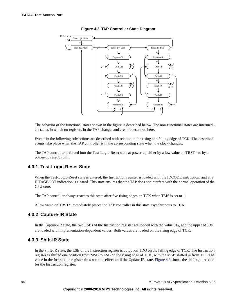
EJTAG Test Access Port
84 MIPS® EJTAG Specification, Revision 5.06
Copyright © 2000-2010 MIPS Technologies Inc. All rights reserved.
Figure 4.2 TAP Controller State Diagram
The behavior of the functional states shown in the figure is described below. The non-functional states are intermedi-ate states in which no registers in the TAP change, and are not described here.
Events in the following subsections are described with relation to the rising and falling edge of TCK. The describedevents take place when the TAP controller is in the corresponding state when the clock changes.
The TAP controller is forced into the Test-Logic-Reset state at power-up either by a low value on TRST* or by apower-up reset circuit.
4.3.1 Test-Logic-Reset State
When the Test-Logic-Reset state is entered, the Instruction register is loaded with the IDCODE instruction, and anyEJTAGBOOT indication is cleared. This state ensures that the TAP does not interfere with the normal operation of theCPU core.
The TAP controller always reaches this state after five rising edges on TCK when TMS is set to 1.
A low value on TRST* immediately places the TAP controller in this state asynchronous to TCK.
4.3.2 Capture-IR State
In the Capture-IR state, the two LSBs of the Instruction register are loaded with the value 012, and the upper MSBsare loaded with implementation-dependent values. Both values are loaded on the rising edge of TCK.
4.3.3 Shift-IR State
In the Shift-IR state, the LSB of the Instruction register is output on TDO on the falling edge of TCK. The Instructionregister is shifted one position from MSB to LSB on the rising edge of TCK, with the MSB shifted in from TDI. Thevalue in the Instruction register does not take effect until the Update-IR state. Figure 4.3 shows the shifting directionfor the Instruction register.
Test-Logic-ResetTMS=1
Run-Test / Idle
0
Select-DR-Scan10
Capture-DR
0
0
Shift-DR
1
Exit1-DR
0
Pause-DR
1
Exit2-DR
1
Update-DR
0
0
01
1
0
1
Select-IR-Scan
Capture-IR
0
0
Shift-IR
1
Exit1-IR
0
Pause-IR
1
Exit2-IR
1
Update-IR
0
0
01
1
0
1
11
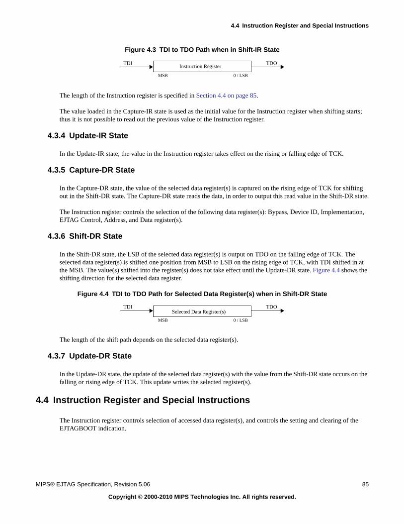
4.4 Instruction Register and Special Instructions
MIPS® EJTAG Specification, Revision 5.06 85
Copyright © 2000-2010 MIPS Technologies Inc. All rights reserved.
Figure 4.3 TDI to TDO Path when in Shift-IR State
The length of the Instruction register is specified in Section 4.4 on page 85.
The value loaded in the Capture-IR state is used as the initial value for the Instruction register when shifting starts;thus it is not possible to read out the previous value of the Instruction register.
4.3.4 Update-IR State
In the Update-IR state, the value in the Instruction register takes effect on the rising or falling edge of TCK.
4.3.5 Capture-DR State
In the Capture-DR state, the value of the selected data register(s) is captured on the rising edge of TCK for shiftingout in the Shift-DR state. The Capture-DR state reads the data, in order to output this read value in the Shift-DR state.
The Instruction register controls the selection of the following data register(s): Bypass, Device ID, Implementation,EJTAG Control, Address, and Data register(s).
4.3.6 Shift-DR State
In the Shift-DR state, the LSB of the selected data register(s) is output on TDO on the falling edge of TCK. Theselected data register(s) is shifted one position from MSB to LSB on the rising edge of TCK, with TDI shifted in atthe MSB. The value(s) shifted into the register(s) does not take effect until the Update-DR state. Figure 4.4 shows theshifting direction for the selected data register.
Figure 4.4 TDI to TDO Path for Selected Data Register(s) when in Shift-DR State
The length of the shift path depends on the selected data register(s).
4.3.7 Update-DR State
In the Update-DR state, the update of the selected data register(s) with the value from the Shift-DR state occurs on thefalling or rising edge of TCK. This update writes the selected register(s).
4.4 Instruction Register and Special Instructions
The Instruction register controls selection of accessed data register(s), and controls the setting and clearing of theEJTAGBOOT indication.
TDIInstruction Register
MSB 0 / LSB
TDO
MSB 0 / LSB
TDI TDOSelected Data Register(s)
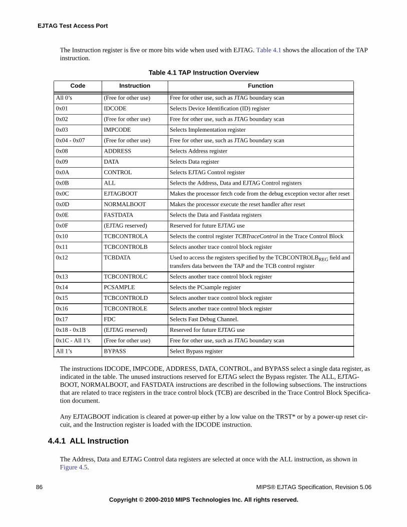
EJTAG Test Access Port
86 MIPS® EJTAG Specification, Revision 5.06
Copyright © 2000-2010 MIPS Technologies Inc. All rights reserved.
The Instruction register is five or more bits wide when used with EJTAG. Table 4.1 shows the allocation of the TAPinstruction.
The instructions IDCODE, IMPCODE, ADDRESS, DATA, CONTROL, and BYPASS select a single data register, asindicated in the table. The unused instructions reserved for EJTAG select the Bypass register. The ALL, EJTAG-BOOT, NORMALBOOT, and FASTDATA instructions are described in the following subsections. The instructionsthat are related to trace registers in the trace control block (TCB) are described in the Trace Control Block Specifica-tion document.
Any EJTAGBOOT indication is cleared at power-up either by a low value on the TRST* or by a power-up reset cir-cuit, and the Instruction register is loaded with the IDCODE instruction.
4.4.1 ALL Instruction
The Address, Data and EJTAG Control data registers are selected at once with the ALL instruction, as shown inFigure 4.5.
Table 4.1 TAP Instruction Overview
Code Instruction Function
All 0’s (Free for other use) Free for other use, such as JTAG boundary scan
0x01 IDCODE Selects Device Identification (ID) register
0x02 (Free for other use) Free for other use, such as JTAG boundary scan
0x03 IMPCODE Selects Implementation register
0x04 - 0x07 (Free for other use) Free for other use, such as JTAG boundary scan
0x08 ADDRESS Selects Address register
0x09 DATA Selects Data register
0x0A CONTROL Selects EJTAG Control register
0x0B ALL Selects the Address, Data and EJTAG Control registers
0x0C EJTAGBOOT Makes the processor fetch code from the debug exception vector after reset
0x0D NORMALBOOT Makes the processor execute the reset handler after reset
0x0E FASTDATA Selects the Data and Fastdata registers
0x0F (EJTAG reserved) Reserved for future EJTAG use
0x10 TCBCONTROLA Selects the control register TCBTraceControl in the Trace Control Block
0x11 TCBCONTROLB Selects another trace control block register
0x12 TCBDATA Used to access the registers specified by the TCBCONTROLBREG field and
transfers data between the TAP and the TCB control register
0x13 TCBCONTROLC Selects another trace control block register
0x14 PCSAMPLE Selects the PCsample register
0x15 TCBCONTROLD Selects another trace control block register
0x16 TCBCONTROLE Selects another trace control block register
0x17 FDC Selects Fast Debug Channel.
0x18 - 0x1B (EJTAG reserved) Reserved for future EJTAG use
0x1C - All 1’s (Free for other use) Free for other use, such as JTAG boundary scan
All 1’s BYPASS Select Bypass register
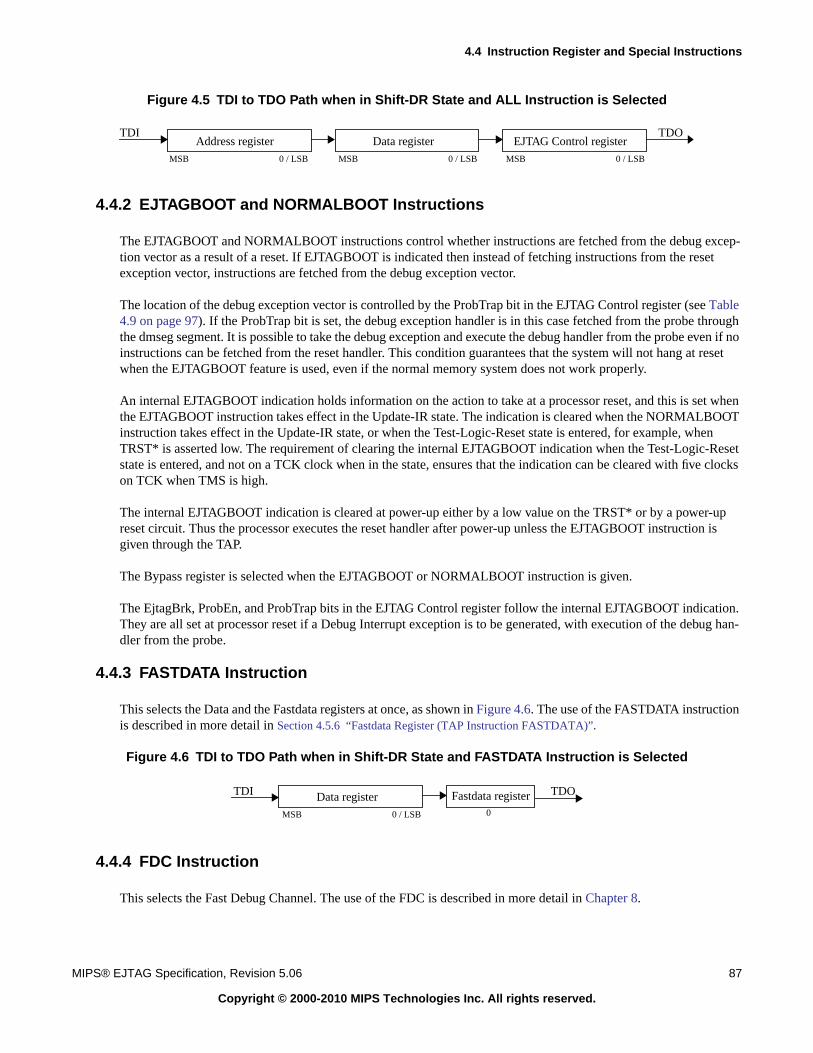
4.4 Instruction Register and Special Instructions
MIPS® EJTAG Specification, Revision 5.06 87
Copyright © 2000-2010 MIPS Technologies Inc. All rights reserved.
Figure 4.5 TDI to TDO Path when in Shift-DR State and ALL Instruction is Selected
4.4.2 EJTAGBOOT and NORMALBOOT Instructions
The EJTAGBOOT and NORMALBOOT instructions control whether instructions are fetched from the debug excep-tion vector as a result of a reset. If EJTAGBOOT is indicated then instead of fetching instructions from the resetexception vector, instructions are fetched from the debug exception vector.
The location of the debug exception vector is controlled by the ProbTrap bit in the EJTAG Control register (see Table4.9 on page 97). If the ProbTrap bit is set, the debug exception handler is in this case fetched from the probe throughthe dmseg segment. It is possible to take the debug exception and execute the debug handler from the probe even if noinstructions can be fetched from the reset handler. This condition guarantees that the system will not hang at resetwhen the EJTAGBOOT feature is used, even if the normal memory system does not work properly.
An internal EJTAGBOOT indication holds information on the action to take at a processor reset, and this is set whenthe EJTAGBOOT instruction takes effect in the Update-IR state. The indication is cleared when the NORMALBOOTinstruction takes effect in the Update-IR state, or when the Test-Logic-Reset state is entered, for example, whenTRST* is asserted low. The requirement of clearing the internal EJTAGBOOT indication when the Test-Logic-Resetstate is entered, and not on a TCK clock when in the state, ensures that the indication can be cleared with five clockson TCK when TMS is high.
The internal EJTAGBOOT indication is cleared at power-up either by a low value on the TRST* or by a power-upreset circuit. Thus the processor executes the reset handler after power-up unless the EJTAGBOOT instruction isgiven through the TAP.
The Bypass register is selected when the EJTAGBOOT or NORMALBOOT instruction is given.
The EjtagBrk, ProbEn, and ProbTrap bits in the EJTAG Control register follow the internal EJTAGBOOT indication.They are all set at processor reset if a Debug Interrupt exception is to be generated, with execution of the debug han-dler from the probe.
4.4.3 FASTDATA Instruction
This selects the Data and the Fastdata registers at once, as shown in Figure 4.6. The use of the FASTDATA instructionis described in more detail in Section 4.5.6 “Fastdata Register (TAP Instruction FASTDATA)”.
Figure 4.6 TDI to TDO Path when in Shift-DR State and FASTDATA Instruction is Selected
4.4.4 FDC Instruction
This selects the Fast Debug Channel. The use of the FDC is described in more detail in Chapter 8.
TDIAddress register EJTAG Control registerData register
TDO
MSB 0 / LSBMSB 0 / LSB MSB 0 / LSB
TDI Fastdata registerData register TDO
MSB 0 / LSB 0
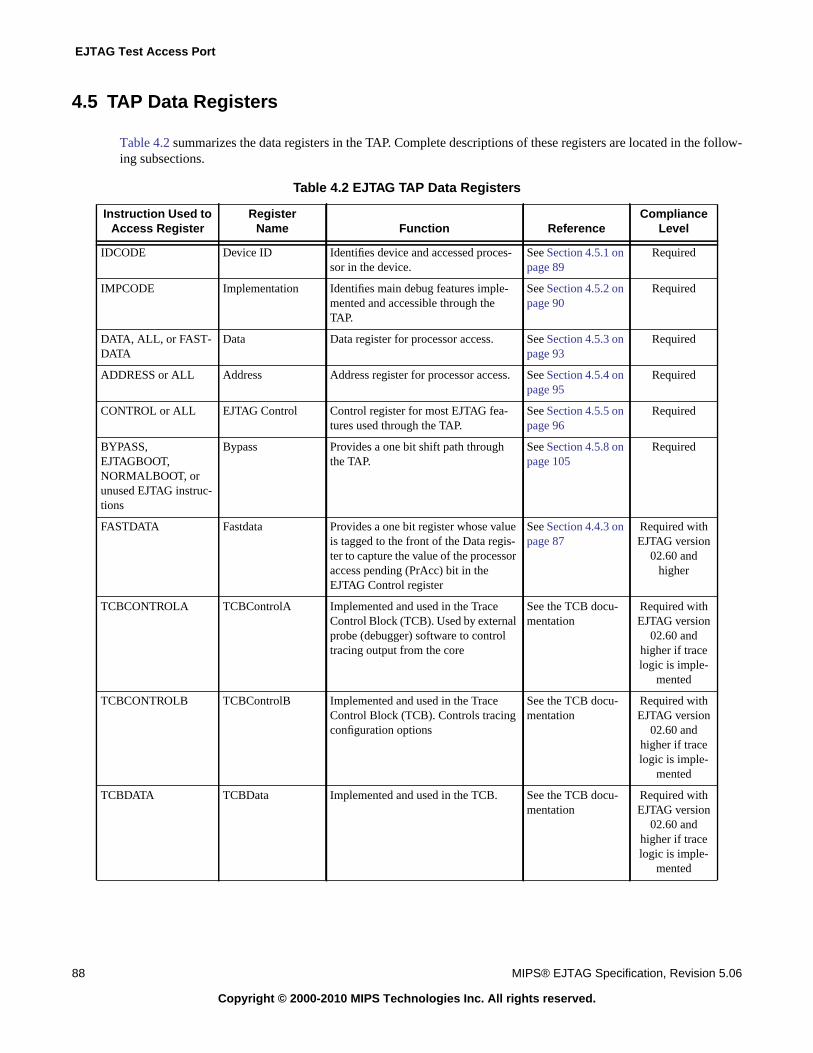
EJTAG Test Access Port
88 MIPS® EJTAG Specification, Revision 5.06
Copyright © 2000-2010 MIPS Technologies Inc. All rights reserved.
4.5 TAP Data Registers
Table 4.2 summarizes the data registers in the TAP. Complete descriptions of these registers are located in the follow-ing subsections.
Table 4.2 EJTAG TAP Data Registers
Instruction Used toAccess Register
RegisterName Function Reference
ComplianceLevel
IDCODE Device ID Identifies device and accessed proces-sor in the device.
See Section 4.5.1 onpage 89
Required
IMPCODE Implementation Identifies main debug features imple-mented and accessible through theTAP.
See Section 4.5.2 onpage 90
Required
DATA, ALL, or FAST-DATA
Data Data register for processor access. See Section 4.5.3 onpage 93
Required
ADDRESS or ALL Address Address register for processor access. See Section 4.5.4 onpage 95
Required
CONTROL or ALL EJTAG Control Control register for most EJTAG fea-tures used through the TAP.
See Section 4.5.5 onpage 96
Required
BYPASS,EJTAGBOOT,NORMALBOOT, orunused EJTAG instruc-tions
Bypass Provides a one bit shift path throughthe TAP.
See Section 4.5.8 onpage 105
Required
FASTDATA Fastdata Provides a one bit register whose valueis tagged to the front of the Data regis-ter to capture the value of the processoraccess pending (PrAcc) bit in theEJTAG Control register
See Section 4.4.3 onpage 87
Required withEJTAG version
02.60 andhigher
TCBCONTROLA TCBControlA Implemented and used in the TraceControl Block (TCB). Used by externalprobe (debugger) software to controltracing output from the core
See the TCB docu-mentation
Required withEJTAG version
02.60 andhigher if tracelogic is imple-
mented
TCBCONTROLB TCBControlB Implemented and used in the TraceControl Block (TCB). Controls tracingconfiguration options
See the TCB docu-mentation
Required withEJTAG version
02.60 andhigher if tracelogic is imple-
mented
TCBDATA TCBData Implemented and used in the TCB. See the TCB docu-mentation
Required withEJTAG version
02.60 andhigher if tracelogic is imple-
mented
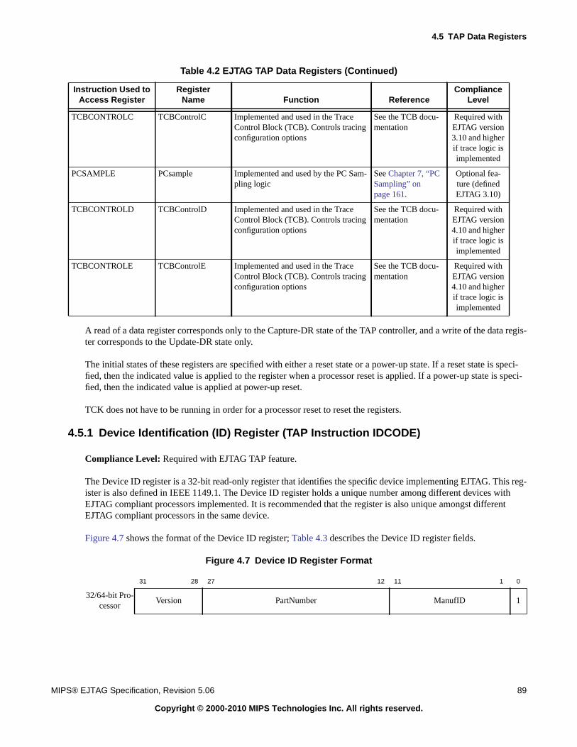
4.5 TAP Data Registers
MIPS® EJTAG Specification, Revision 5.06 89
Copyright © 2000-2010 MIPS Technologies Inc. All rights reserved.
A read of a data register corresponds only to the Capture-DR state of the TAP controller, and a write of the data regis-ter corresponds to the Update-DR state only.
The initial states of these registers are specified with either a reset state or a power-up state. If a reset state is speci-fied, then the indicated value is applied to the register when a processor reset is applied. If a power-up state is speci-fied, then the indicated value is applied at power-up reset.
TCK does not have to be running in order for a processor reset to reset the registers.
4.5.1 Device Identification (ID) Register (TAP Instruction IDCODE)
Compliance Level: Required with EJTAG TAP feature.
The Device ID register is a 32-bit read-only register that identifies the specific device implementing EJTAG. This reg-ister is also defined in IEEE 1149.1. The Device ID register holds a unique number among different devices withEJTAG compliant processors implemented. It is recommended that the register is also unique amongst differentEJTAG compliant processors in the same device.
Figure 4.7 shows the format of the Device ID register; Table 4.3 describes the Device ID register fields.
Figure 4.7 Device ID Register Format
TCBCONTROLC TCBControlC Implemented and used in the TraceControl Block (TCB). Controls tracingconfiguration options
See the TCB docu-mentation
Required withEJTAG version3.10 and higherif trace logic isimplemented
PCSAMPLE PCsample Implemented and used by the PC Sam-pling logic
See Chapter 7, “PCSampling” onpage 161.
Optional fea-ture (definedEJTAG 3.10)
TCBCONTROLD TCBControlD Implemented and used in the TraceControl Block (TCB). Controls tracingconfiguration options
See the TCB docu-mentation
Required withEJTAG version4.10 and higherif trace logic isimplemented
TCBCONTROLE TCBControlE Implemented and used in the TraceControl Block (TCB). Controls tracingconfiguration options
See the TCB docu-mentation
Required withEJTAG version4.10 and higherif trace logic isimplemented
31 28 27 12 11 1 0
32/64-bit Pro-cessor
Version PartNumber ManufID 1
Table 4.2 EJTAG TAP Data Registers (Continued)
Instruction Used toAccess Register
RegisterName Function Reference
ComplianceLevel
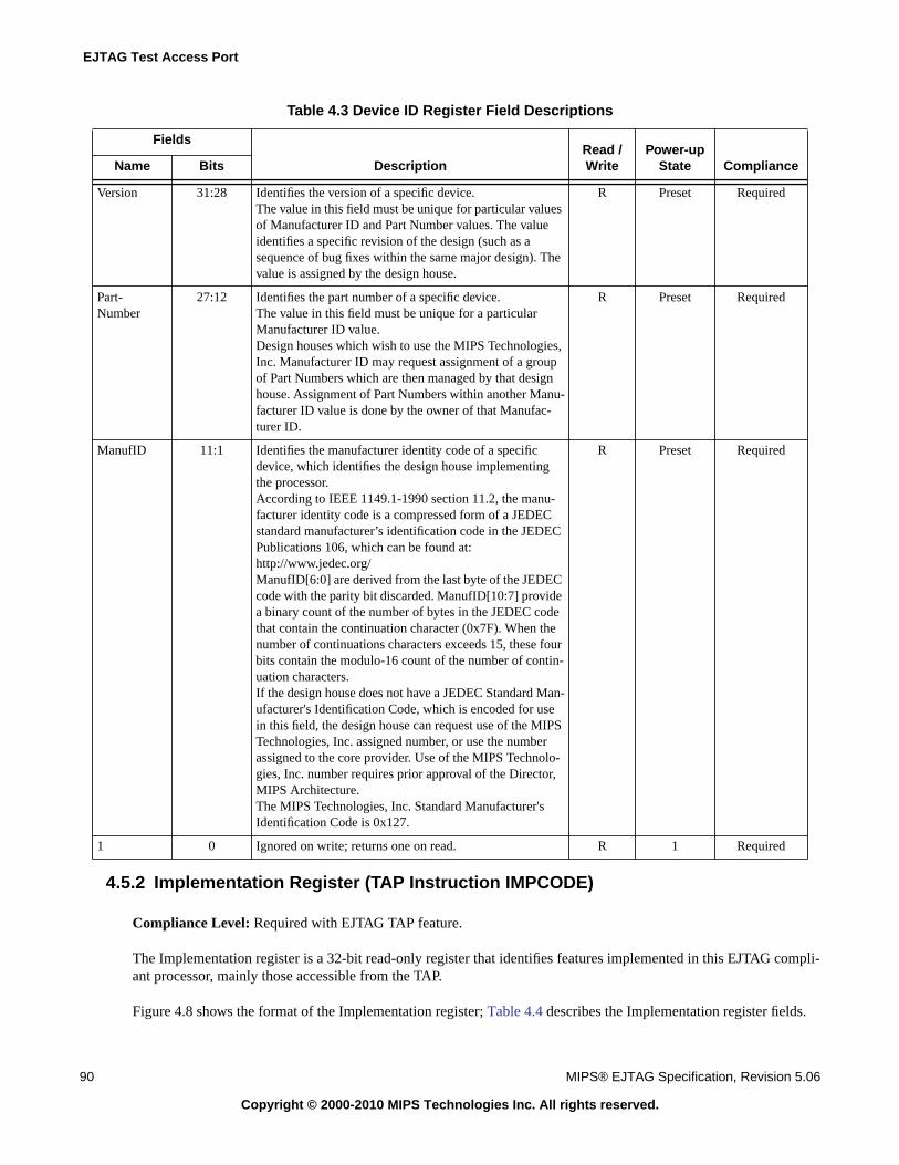
EJTAG Test Access Port
90 MIPS® EJTAG Specification, Revision 5.06
Copyright © 2000-2010 MIPS Technologies Inc. All rights reserved.
4.5.2 Implementation Register (TAP Instruction IMPCODE)
Compliance Level: Required with EJTAG TAP feature.
The Implementation register is a 32-bit read-only register that identifies features implemented in this EJTAG compli-ant processor, mainly those accessible from the TAP.
Figure 4.8 shows the format of the Implementation register; Table 4.4 describes the Implementation register fields.
Table 4.3 Device ID Register Field Descriptions
Fields
DescriptionRead /Write
Power-upState ComplianceName Bits
Version 31:28 Identifies the version of a specific device.The value in this field must be unique for particular valuesof Manufacturer ID and Part Number values. The valueidentifies a specific revision of the design (such as asequence of bug fixes within the same major design). Thevalue is assigned by the design house.
R Preset Required
Part-Number
27:12 Identifies the part number of a specific device.The value in this field must be unique for a particularManufacturer ID value.Design houses which wish to use the MIPS Technologies,Inc. Manufacturer ID may request assignment of a groupof Part Numbers which are then managed by that designhouse. Assignment of Part Numbers within another Manu-facturer ID value is done by the owner of that Manufac-turer ID.
R Preset Required
ManufID 11:1 Identifies the manufacturer identity code of a specificdevice, which identifies the design house implementingthe processor.According to IEEE 1149.1-1990 section 11.2, the manu-facturer identity code is a compressed form of a JEDECstandard manufacturer’s identification code in the JEDECPublications 106, which can be found at:http://www.jedec.org/ManufID[6:0] are derived from the last byte of the JEDECcode with the parity bit discarded. ManufID[10:7] providea binary count of the number of bytes in the JEDEC codethat contain the continuation character (0x7F). When thenumber of continuations characters exceeds 15, these fourbits contain the modulo-16 count of the number of contin-uation characters.If the design house does not have a JEDEC Standard Man-ufacturer's Identification Code, which is encoded for usein this field, the design house can request use of the MIPSTechnologies, Inc. assigned number, or use the numberassigned to the core provider. Use of the MIPS Technolo-gies, Inc. number requires prior approval of the Director,MIPS Architecture.The MIPS Technologies, Inc. Standard Manufacturer'sIdentification Code is 0x127.
R Preset Required
1 0 Ignored on write; returns one on read. R 1 Required
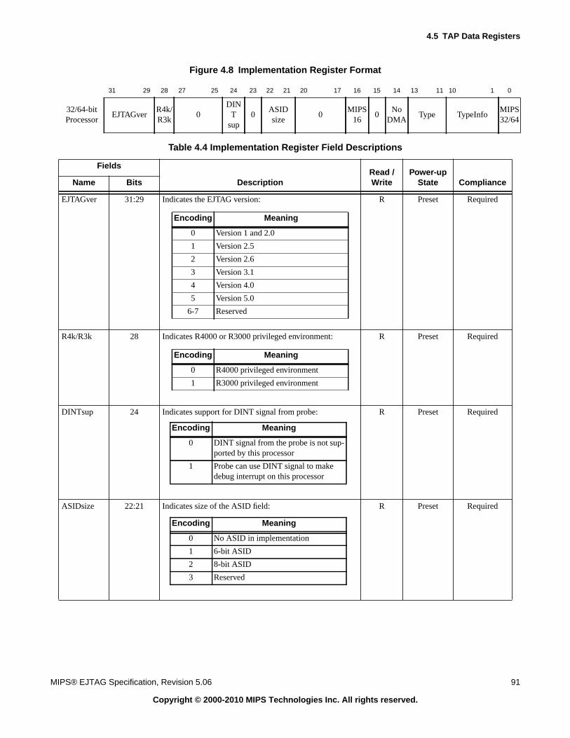
4.5 TAP Data Registers
MIPS® EJTAG Specification, Revision 5.06 91
Copyright © 2000-2010 MIPS Technologies Inc. All rights reserved.
Figure 4.8 Implementation Register Format
31 29 28 27 25 24 23 22 21 20 17 16 15 14 13 11 10 1 0
32/64-bitProcessor
EJTAGverR4k/R3k
0DIN
Tsup
0ASIDsize
0MIPS
160
NoDMA
Type TypeInfoMIPS32/64
Table 4.4 Implementation Register Field Descriptions
Fields
DescriptionRead /Write
Power-upState ComplianceName Bits
EJTAGver 31:29 Indicates the EJTAG version: R Preset Required
R4k/R3k 28 Indicates R4000 or R3000 privileged environment: R Preset Required
DINTsup 24 Indicates support for DINT signal from probe: R Preset Required
ASIDsize 22:21 Indicates size of the ASID field: R Preset Required
Encoding Meaning
0 Version 1 and 2.0
1 Version 2.5
2 Version 2.6
3 Version 3.1
4 Version 4.0
5 Version 5.0
6-7 Reserved
Encoding Meaning
0 R4000 privileged environment
1 R3000 privileged environment
Encoding Meaning
0 DINT signal from the probe is not sup-ported by this processor
1 Probe can use DINT signal to makedebug interrupt on this processor
Encoding Meaning
0 No ASID in implementation
1 6-bit ASID
2 8-bit ASID
3 Reserved
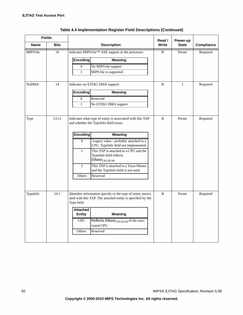
EJTAG Test Access Port
92 MIPS® EJTAG Specification, Revision 5.06
Copyright © 2000-2010 MIPS Technologies Inc. All rights reserved.
MIPS16e 16 Indicates MIPS16e™ ASE support in the processor: R Preset Required
NoDMA 14 Indicates no EJTAG DMA support: R 1 Required
Type 13:11 Indicates what type of entity is associated with this TAPand whether the TypeInfo field exists.
R Preset Required
TypeInfo 10:1 Identifier information specific to the type of entity associ-ated with this TAP. The attached entity is specified by theType field.
R Preset Required
Table 4.4 Implementation Register Field Descriptions (Continued)
Fields
DescriptionRead /Write
Power-upState ComplianceName Bits
Encoding Meaning
0 No MIPS16e support
1 MIPS16e is supported
Encoding Meaning
0 Reserved
1 No EJTAG DMA support
Encoding Meaning
0 Legacy value - probably attached to aCPU. TypeInfo field not implemented.
1 This TAP is attached to a CPU and theTypeInfo field reflectsEBaseCPUNUM.
2 This TAP is attached to a Trace-Masterand the TypeInfo field is not used.
Others Reserved
AttachedEntity Meaning
CPU Reflects EBaseCPUNUM of the asso-
ciated CPU
Others Reserved
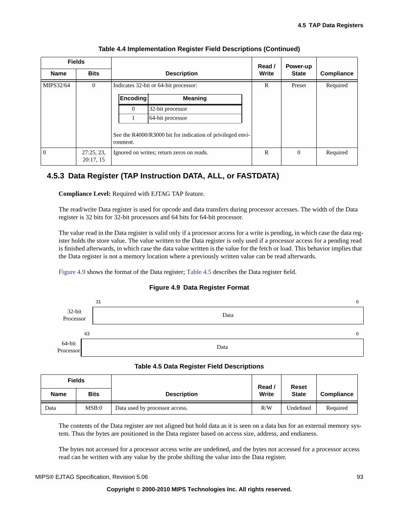
4.5 TAP Data Registers
MIPS® EJTAG Specification, Revision 5.06 93
Copyright © 2000-2010 MIPS Technologies Inc. All rights reserved.
4.5.3 Data Register (TAP Instruction DATA, ALL, or FASTDATA)
Compliance Level: Required with EJTAG TAP feature.
The read/write Data register is used for opcode and data transfers during processor accesses. The width of the Dataregister is 32 bits for 32-bit processors and 64 bits for 64-bit processor.
The value read in the Data register is valid only if a processor access for a write is pending, in which case the data reg-ister holds the store value. The value written to the Data register is only used if a processor access for a pending readis finished afterwards, in which case the data value written is the value for the fetch or load. This behavior implies thatthe Data register is not a memory location where a previously written value can be read afterwards.
Figure 4.9 shows the format of the Data register; Table 4.5 describes the Data register field.
Figure 4.9 Data Register Format
The contents of the Data register are not aligned but hold data as it is seen on a data bus for an external memory sys-tem. Thus the bytes are positioned in the Data register based on access size, address, and endianess.
The bytes not accessed for a processor access write are undefined, and the bytes not accessed for a processor accessread can be written with any value by the probe shifting the value into the Data register.
MIPS32/64 0 Indicates 32-bit or 64-bit processor:
See the R4000/R3000 bit for indication of privileged envi-ronment.
R Preset Required
0 27:25, 23,20:17, 15
Ignored on writes; return zeros on reads. R 0 Required
31 0
32-bitProcessor
Data
63 0
64-bitProcessor
Data
Table 4.5 Data Register Field Descriptions
Fields
DescriptionRead /Write
ResetState ComplianceName Bits
Data MSB:0 Data used by processor access. R/W Undefined Required
Table 4.4 Implementation Register Field Descriptions (Continued)
Fields
DescriptionRead /Write
Power-upState ComplianceName Bits
Encoding Meaning
0 32-bit processor
1 64-bit processor
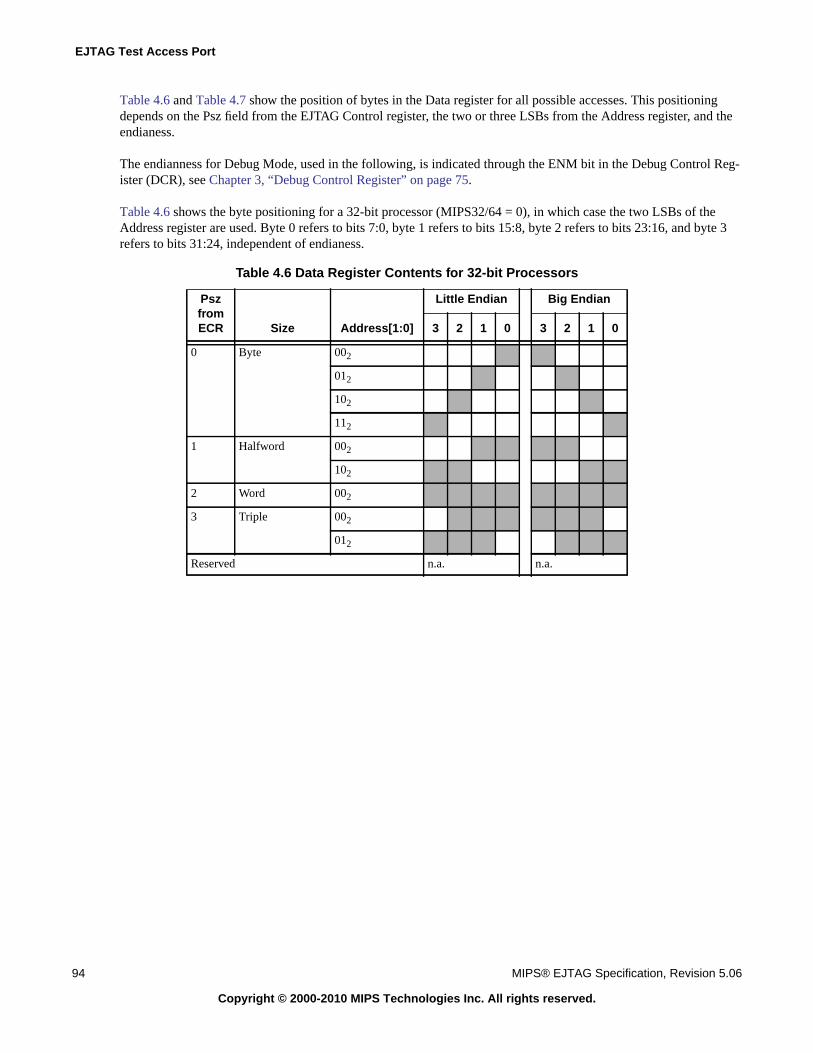
EJTAG Test Access Port
94 MIPS® EJTAG Specification, Revision 5.06
Copyright © 2000-2010 MIPS Technologies Inc. All rights reserved.
Table 4.6 and Table 4.7 show the position of bytes in the Data register for all possible accesses. This positioningdepends on the Psz field from the EJTAG Control register, the two or three LSBs from the Address register, and theendianess.
The endianness for Debug Mode, used in the following, is indicated through the ENM bit in the Debug Control Reg-ister (DCR), see Chapter 3, “Debug Control Register” on page 75.
Table 4.6 shows the byte positioning for a 32-bit processor (MIPS32/64 = 0), in which case the two LSBs of theAddress register are used. Byte 0 refers to bits 7:0, byte 1 refers to bits 15:8, byte 2 refers to bits 23:16, and byte 3refers to bits 31:24, independent of endianess.
Table 4.6 Data Register Contents for 32-bit Processors
PszfromECR Size Address[1:0]
Little Endian Big Endian
3 2 1 0 3 2 1 0
0 Byte 002
012
102
112
1 Halfword 002
102
2 Word 002
3 Triple 002
012
Reserved n.a. n.a.
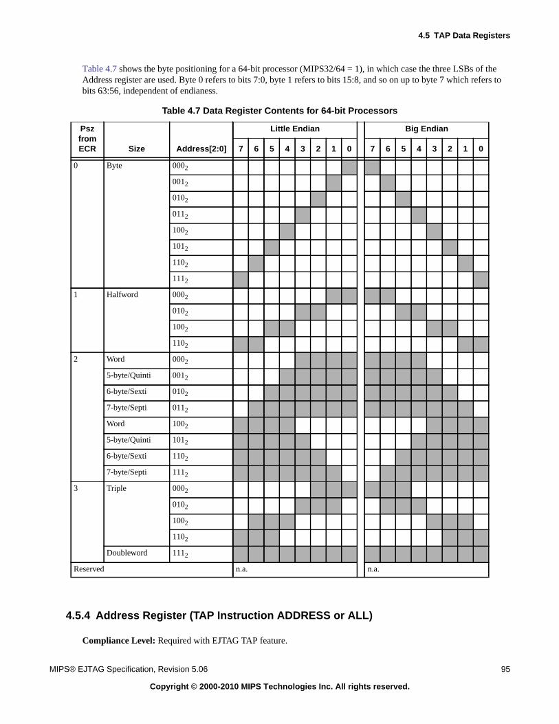
4.5 TAP Data Registers
MIPS® EJTAG Specification, Revision 5.06 95
Copyright © 2000-2010 MIPS Technologies Inc. All rights reserved.
Table 4.7 shows the byte positioning for a 64-bit processor (MIPS32/64 = 1), in which case the three LSBs of theAddress register are used. Byte 0 refers to bits 7:0, byte 1 refers to bits 15:8, and so on up to byte 7 which refers tobits 63:56, independent of endianess.
4.5.4 Address Register (TAP Instruction ADDRESS or ALL)
Compliance Level: Required with EJTAG TAP feature.
Table 4.7 Data Register Contents for 64-bit Processors
PszfromECR Size Address[2:0]
Little Endian Big Endian
7 6 5 4 3 2 1 0 7 6 5 4 3 2 1 0
0 Byte 0002
0012
0102
0112
1002
1012
1102
1112
1 Halfword 0002
0102
1002
1102
2 Word 0002
5-byte/Quinti 0012
6-byte/Sexti 0102
7-byte/Septi 0112
Word 1002
5-byte/Quinti 1012
6-byte/Sexti 1102
7-byte/Septi 1112
3 Triple 0002
0102
1002
1102
Doubleword 1112
Reserved n.a. n.a.
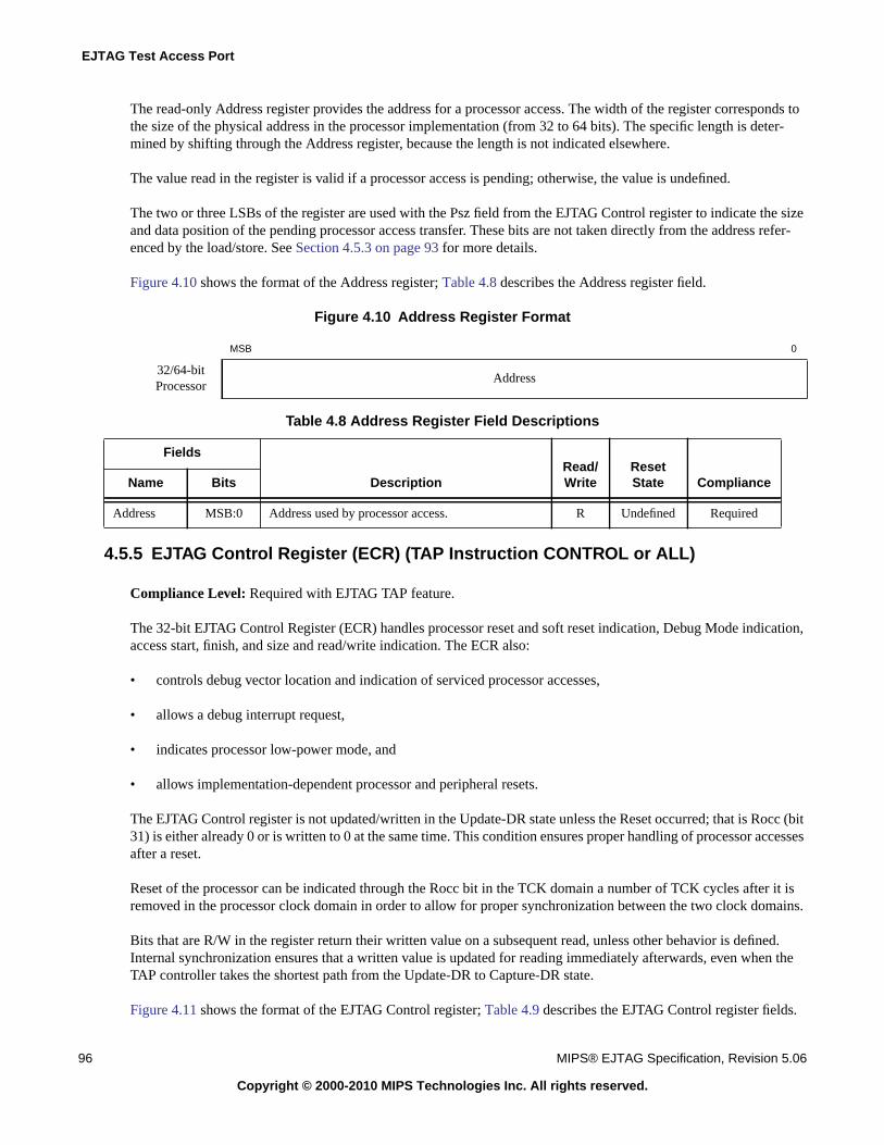
EJTAG Test Access Port
96 MIPS® EJTAG Specification, Revision 5.06
Copyright © 2000-2010 MIPS Technologies Inc. All rights reserved.
The read-only Address register provides the address for a processor access. The width of the register corresponds tothe size of the physical address in the processor implementation (from 32 to 64 bits). The specific length is deter-mined by shifting through the Address register, because the length is not indicated elsewhere.
The value read in the register is valid if a processor access is pending; otherwise, the value is undefined.
The two or three LSBs of the register are used with the Psz field from the EJTAG Control register to indicate the sizeand data position of the pending processor access transfer. These bits are not taken directly from the address refer-enced by the load/store. See Section 4.5.3 on page 93 for more details.
Figure 4.10 shows the format of the Address register; Table 4.8 describes the Address register field.
Figure 4.10 Address Register Format
4.5.5 EJTAG Control Register (ECR) (TAP Instruction CONTROL or ALL)
Compliance Level: Required with EJTAG TAP feature.
The 32-bit EJTAG Control Register (ECR) handles processor reset and soft reset indication, Debug Mode indication,access start, finish, and size and read/write indication. The ECR also:
• controls debug vector location and indication of serviced processor accesses,
• allows a debug interrupt request,
• indicates processor low-power mode, and
• allows implementation-dependent processor and peripheral resets.
The EJTAG Control register is not updated/written in the Update-DR state unless the Reset occurred; that is Rocc (bit31) is either already 0 or is written to 0 at the same time. This condition ensures proper handling of processor accessesafter a reset.
Reset of the processor can be indicated through the Rocc bit in the TCK domain a number of TCK cycles after it isremoved in the processor clock domain in order to allow for proper synchronization between the two clock domains.
Bits that are R/W in the register return their written value on a subsequent read, unless other behavior is defined.Internal synchronization ensures that a written value is updated for reading immediately afterwards, even when theTAP controller takes the shortest path from the Update-DR to Capture-DR state.
Figure 4.11 shows the format of the EJTAG Control register; Table 4.9 describes the EJTAG Control register fields.
MSB 0
32/64-bitProcessor
Address
Table 4.8 Address Register Field Descriptions
Fields
DescriptionRead/Write
ResetState ComplianceName Bits
Address MSB:0 Address used by processor access. R Undefined Required
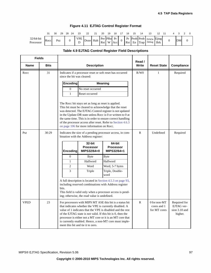
4.5 TAP Data Registers
MIPS® EJTAG Specification, Revision 5.06 97
Copyright © 2000-2010 MIPS Technologies Inc. All rights reserved.
Figure 4.11 EJTAG Control Register Format
31 30 29 28 24 23 22 21 20 19 18 17 16 15 14 13 12 11 4 3 2 0
32/64-bitProcessor
Rocc Psz 0VPE
DDoze Halt
PerRst
PRnW
PrAcc
0PrRst
ProbEn
ProbTrap
ISAOnDebug
EjtagBrk
0 DM 0
Table 4.9 EJTAG Control Register Field Descriptions
Fields
DescriptionRead /Write Reset State ComplianceName Bits
Rocc 31 Indicates if a processor reset or soft reset has occurredsince the bit was cleared:
The Rocc bit stays set as long as reset is applied.This bit must be cleared to acknowledge that the resetwas detected. The EJTAG Control register is not updatedin the Update-DR state unless Rocc is 0 or written to 0 atthe same time. This is in order to ensure correct handlingof the processor access after reset. Refer to Section 4.6.3on page 106 for more information on Rocc.
R/W0 1 Required
Psz 30:29 Indicates the size of a pending processor access, in com-bination with the Address register:
A full description is located in Section 4.5.3 on page 93,including reserved combinations with Address registerbits.This field is valid only when a processor access is pend-ing; otherwise, the read value is undefined.
R Undefined Required
VPED 23 For processors with MIPS MT ASE this bit is a status bitthat indicates whether the VPE is currently disabled. Avalue of 1 indicates that the VPE is disabled and the restof the EJTAG state is not valid. If this bit is 0, then theprocessor is either not a MT core or it is an MT core thatis currently enabled. Hence, a non-MT core must imple-ment this bit and tie it to zero.
R 0 for non-MTcores and 1
for MT cores
Required forEJTAG ver-
sion 3.10 andhigher.
Encoding Meaning
0 No reset occurred
1 Reset occurred
Encoding
32-bitProcessor
MIPS32/64=0
64-bitProcessor
MIPS32/64=1
0 Byte Byte
1 Halfword Halfword
2 Word Word, 5-7 bytes
3 Triple Triple, Double-word
EJTAG Test Access Port
98 MIPS® EJTAG Specification, Revision 5.06
Copyright © 2000-2010 MIPS Technologies Inc. All rights reserved.
Doze 22 Indicates if the processor is in low-power mode:
Doze indicates Reduced Power (RP) and WAIT, andother implementation-dependent low-power modes.If the implementation does not support low-powermodes, then this bit always reads as 0.
R 0 Required
Halt 21 Indicates if the internal system bus clock is running:
Halt indicates WAIT, and other implementation-depen-dent events that stop the system bus clock.If the implementation does not support a halt state, thenthe bit always reads as 0.
R 0 Required
PerRst 20 Controls the peripheral reset with implementa-tion-dependent behavior:
This bit PerRst might not have any effect. There is noinherent indication of whether the PerRst is effective, sothe user must consult system documentation.When this bit is changed, then it is only guaranteed thatthe new value has taken effect when it can be read backhere. This handshake mechanism ensures that the settingfrom the TCK clock domain takes effect in the processorclock domain and in peripherals.This bit is read-only (R) and reads as zero if not imple-mented.
R/W 0 Optional
Table 4.9 EJTAG Control Register Field Descriptions (Continued)
Fields
DescriptionRead /Write Reset State ComplianceName Bits
Encoding Meaning
0 Processor is not in low-power mode
1 Processor is in low-power mode
Encoding Meaning
0 Internal system bus clock is running
1 Internal system bus clock is stopped
Encoding Meaning
0 No peripheral reset applied
1 Peripheral reset applied
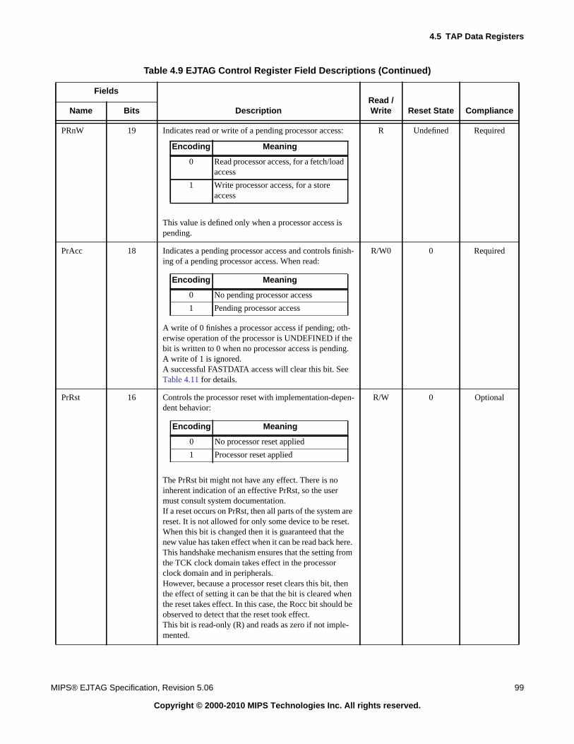
4.5 TAP Data Registers
MIPS® EJTAG Specification, Revision 5.06 99
Copyright © 2000-2010 MIPS Technologies Inc. All rights reserved.
PRnW 19 Indicates read or write of a pending processor access:
This value is defined only when a processor access ispending.
R Undefined Required
PrAcc 18 Indicates a pending processor access and controls finish-ing of a pending processor access. When read:
A write of 0 finishes a processor access if pending; oth-erwise operation of the processor is UNDEFINED if thebit is written to 0 when no processor access is pending.A write of 1 is ignored.A successful FASTDATA access will clear this bit. SeeTable 4.11 for details.
R/W0 0 Required
PrRst 16 Controls the processor reset with implementation-depen-dent behavior:
The PrRst bit might not have any effect. There is noinherent indication of an effective PrRst, so the usermust consult system documentation.If a reset occurs on PrRst, then all parts of the system arereset. It is not allowed for only some device to be reset.When this bit is changed then it is guaranteed that thenew value has taken effect when it can be read back here.This handshake mechanism ensures that the setting fromthe TCK clock domain takes effect in the processorclock domain and in peripherals.However, because a processor reset clears this bit, thenthe effect of setting it can be that the bit is cleared whenthe reset takes effect. In this case, the Rocc bit should beobserved to detect that the reset took effect.This bit is read-only (R) and reads as zero if not imple-mented.
R/W 0 Optional
Table 4.9 EJTAG Control Register Field Descriptions (Continued)
Fields
DescriptionRead /Write Reset State ComplianceName Bits
Encoding Meaning
0 Read processor access, for a fetch/loadaccess
1 Write processor access, for a storeaccess
Encoding Meaning
0 No pending processor access
1 Pending processor access
Encoding Meaning
0 No processor reset applied
1 Processor reset applied
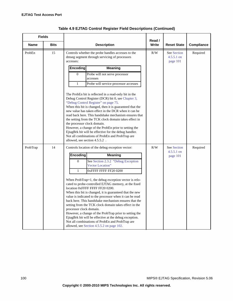
EJTAG Test Access Port
100 MIPS® EJTAG Specification, Revision 5.06
Copyright © 2000-2010 MIPS Technologies Inc. All rights reserved.
ProbEn 15 Controls whether the probe handles accesses to thedmseg segment through servicing of processorsaccesses:
The ProbEn bit is reflected in a read-only bit in theDebug Control Register (DCR) bit 0, see Chapter 3,“Debug Control Register” on page 75.When this bit is changed, then it is guaranteed that thenew value has taken effect in the DCR when it can beread back here. This handshake mechanism ensures thatthe setting from the TCK clock domain takes effect inthe processor clock domain.However, a change of the ProbEn prior to setting theEjtagBrk bit will be effective for the debug handler.Not all combinations of ProbEn and ProbTrap areallowed, see section 4.5.5.2 .
R/W See Section4.5.5.1 onpage 101
Required
ProbTrap 14 Controls location of the debug exception vector:
When ProbTrap=1, the debug exception vector is relo-cated to probe-controlled EJTAG memory, at the fixedlocation 0xFFFF FFFF FF20 0200.When this bit is changed, it is guaranteed that the newvalue is indicated to the processor when it can be readback here. This handshake mechanism ensures that thesetting from the TCK clock domain takes effect in theprocessor clock domain.However, a change of the ProbTrap prior to setting theEjtagBrk bit will be effective at the debug exception.Not all combinations of ProbEn and ProbTrap areallowed, see Section 4.5.5.2 on page 102.
R/W See Section4.5.5.1 onpage 101
Required
Table 4.9 EJTAG Control Register Field Descriptions (Continued)
Fields
DescriptionRead /Write Reset State ComplianceName Bits
Encoding Meaning
0 Probe will not serve processoraccesses
1 Probe will service processor accesses
Encoding Meaning
0 See Section 2.3.2 “Debug ExceptionVector Location”
1 0xFFFF FFFF FF20 0200
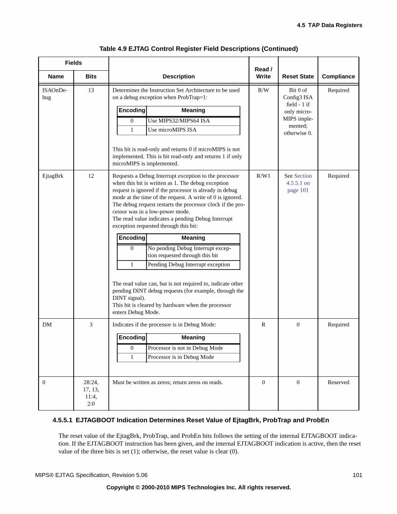
4.5 TAP Data Registers
MIPS® EJTAG Specification, Revision 5.06 101
Copyright © 2000-2010 MIPS Technologies Inc. All rights reserved.
4.5.5.1 EJTAGBOOT Indication Determines Reset Value of EjtagBrk, ProbTrap and ProbEn
The reset value of the EjtagBrk, ProbTrap, and ProbEn bits follows the setting of the internal EJTAGBOOT indica-tion. If the EJTAGBOOT instruction has been given, and the internal EJTAGBOOT indication is active, then the resetvalue of the three bits is set (1); otherwise, the reset value is clear (0).
ISAOnDe-bug
13 Determines the Instruction Set Architecture to be usedon a debug exception when ProbTrap=1:
This bit is read-only and returns 0 if microMIPS is notimplemented. This is bit read-only and returns 1 if onlymicroMIPS is implemented.
R/W Bit 0 ofConfig3 ISA
field - 1 ifonly micro-
MIPS imple-mented;
otherwise 0.
Required
EjtagBrk 12 Requests a Debug Interrupt exception to the processorwhen this bit is written as 1. The debug exceptionrequest is ignored if the processor is already in debugmode at the time of the request. A write of 0 is ignored.The debug request restarts the processor clock if the pro-cessor was in a low-power mode.The read value indicates a pending Debug Interruptexception requested through this bit:
The read value can, but is not required to, indicate otherpending DINT debug requests (for example, through theDINT signal).This bit is cleared by hardware when the processorenters Debug Mode.
R/W1 See Section4.5.5.1 onpage 101
Required
DM 3 Indicates if the processor is in Debug Mode: R 0 Required
0 28:24,17, 13,11:4,2:0
Must be written as zeros; return zeros on reads. 0 0 Reserved
Table 4.9 EJTAG Control Register Field Descriptions (Continued)
Fields
DescriptionRead /Write Reset State ComplianceName Bits
Encoding Meaning
0 Use MIPS32/MIPS64 ISA
1 Use microMIPS ISA
Encoding Meaning
0 No pending Debug Interrupt excep-tion requested through this bit
1 Pending Debug Interrupt exception
Encoding Meaning
0 Processor is not in Debug Mode
1 Processor is in Debug Mode

EJTAG Test Access Port
102 MIPS® EJTAG Specification, Revision 5.06
Copyright © 2000-2010 MIPS Technologies Inc. All rights reserved.
The results of setting these bits are:
• Setting the EjtagBrk causes a Debug Interrupt exception to be requested right after the processor reset from theEJTAGBOOT instruction
• The debug handler is executed from the EJTAG memory because ProbTrap is set to indicate debug vector inEJTAG memory at 0xFFFF FFFF FF20 0200
• Service of the processor access is indicated because ProbEn is set
Thus it is possible to execute the debug handler right after a processor reset from the EJTAGBOOT instruction, with-out executing any instructions from the normal reset handler.
4.5.5.2 Combinations of ProbTrap and ProbEn
Use of ProbTrap and ProbEn allows independent specification of the debug exception vector location and availabilityof EJTAG memory. Behavior for the different combinations is shown in Table 4.10. Note that not all combinationsare allowed. The second combination shown in the table, that is ProbTrap is 0 and ProbEn is 1, puts the debug handlerin normal memory, but also makes the probe’s EJTAG memory available. This combination can be useful, becausedebug handler execution benefits from the speed of normal memory, but the probe’s EJTAG memory can still beaccessed, for example to save/restore data values and for probe/handler communications.
4.5.6 Fastdata Register (TAP Instruction FASTDATA)
Compliance Level: Required with EJTAG TAP feature for EJTAG version 02.60 and higher.
The width of the Fastdata register is 1 bit. During a Fastdata access, the Fastdata register is written and read, i.e., a bitis shifted in and a bit is shifted out. (See Section 4.4.3 on page 87 for how the Data + Fastdata registers are selected bythe FASTDATA instruction.) During a Fastdata access, the Fastdata register value shifted in specifies whether theFastdata access should be completed or not. The value shifted out is a flag that indicates whether the Fastdata accesswas successful or not (if completion was requested).
Figure 4.12 Fastdata Register Format
Table 4.10 Combinations of ProbTrap and ProbEn
ProbTrap ProbEn Debug Exception VectorProcessor Accesses toEJTAG memory region
0 0 Normal memory, Section 2.3.2 “Debug ExceptionVector Location”
Not serviced by probe
0 1 Serviced by probe
1 0 If these two bits are changed to this state, the operation of the processor is UNDEFINED,indicating that the debug exception vector is in EJTAG memory, but the probe will not ser-vice processor accesses.
1 1 EJTAG memory at 0xFFFF FFFF FF20 0200 Serviced by probe
0
32/64-bitProcessor
SPrAcc
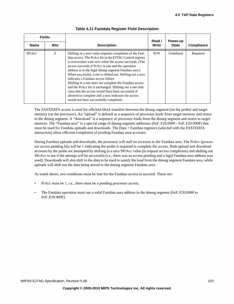
4.5 TAP Data Registers
MIPS® EJTAG Specification, Revision 5.06 103
Copyright © 2000-2010 MIPS Technologies Inc. All rights reserved.
The FASTDATA access is used for efficient block transfers between the dmseg segment (on the probe) and targetmemory (on the processor). An “upload” is defined as a sequence of processor loads from target memory and storesto the dmseg segment. A “download” is a sequence of processor loads from the dmseg segment and stores to targetmemory. The “Fastdata area” is a special range of dmseg segment addresses (0xF..F20.0000 - 0xF..F20.000F) thatmust be used for Fastdata uploads and downloads. The Data + Fastdata registers (selected with the FASTDATAinstruction) allow efficient completion of pending Fastdata area accesses.
During Fastdata uploads and downloads, the processor will stall on accesses to the Fastdata area. The PrAcc (proces-sor access pending bit) will be 1 indicating the probe is required to complete the access. Both upload and downloadaccesses by the probe are attempted by shifting in a zero SPrAcc value (to request access completion) and shifting outSPrAcc to see if the attempt will be successful (i.e., there was an access pending and a legal Fastdata area address wasused). Downloads will also shift in the data to be used to satisfy the load from the dmseg segment Fastdata area, whileuploads will shift out the data being stored to the dmseg segment Fastdata area.
As noted above, two conditions must be true for the Fastdata access to succeed. These are:
• PrAcc must be 1, i.e., there must be a pending processor access.
• The Fastdata operation must use a valid Fastdata area address in the dmseg segment (0xF..F20.0000 to0xF..F20.000F).
Table 4.11 Fastdata Register Field Description
Fields
DescriptionRead /Write
Power-upState ComplianceName Bits
SPrAcc 0 Shifting in a zero value requests completion of the Fast-data access. The PrAcc bit in the EJTAG Control registeris overwritten with zero when the access succeeds. (Theaccess succeeds if PrAcc is one and the operationaddress is in the legal dmseg segment Fastdata area.)When successful, a one is shifted out. Shifting out a zeroindicates a Fastdata access failure.Shifting in a one does not complete the Fastdata accessand the PrAcc bit is unchanged. Shifting out a one indi-cates that the access would have been successful ifallowed to complete and a zero indicates the accesswould not have successfully completed.
R/W Undefined Required
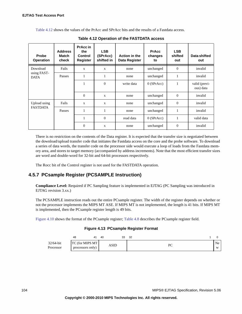
EJTAG Test Access Port
104 MIPS® EJTAG Specification, Revision 5.06
Copyright © 2000-2010 MIPS Technologies Inc. All rights reserved.
Table 4.12 shows the values of the PrAcc and SPrAcc bits and the results of a Fastdata access.
There is no restriction on the contents of the Data register. It is expected that the transfer size is negotiated betweenthe download/upload transfer code that initiates the Fastdata access on the core and the probe software. To downloada series of data words, the transfer code on the processor side would execute a loop of loads from the Fastdata mem-ory area, and stores to target memory (accompanied by address increments). Note that the most efficient transfer sizesare word and double-word for 32-bit and 64-bit processors respectively.
The Rocc bit of the Control register is not used for the FASTDATA operation.
4.5.7 PCsample Register (PCSAMPLE Instruction)
Compliance Level: Required if PC Sampling feature is implemented in EJTAG (PC Sampling was introduced inEJTAG revision 3.xx.)
The PCSAMPLE instruction reads out the entire PCsample register. The width of the register depends on whether ornot the processor implements the MIPS MT ASE. If MIPS MT is not implemented, the length is 41 bits. If MIPS MTis implemented, then the PCsample register length is 49 bits.
Figure 4.10 shows the format of the PCsample register; Table 4.8 describes the PCsample register field.
Figure 4.13 PCsample Register Format
Table 4.12 Operation of the FASTDATA access
ProbeOperation
AddressMatchcheck
PrAcc inthe
ControlRegister
LSB(SPrAcc)shifted in
Action in theData Register
PrAccchanges
to
LSBshifted
outData shifted
out
Downloadusing FAST-DATA
Fails x x none unchanged 0 invalid
Passes 1 1 none unchanged 1 invalid
1 0 write data 0 (SPrAcc) 1 valid (previ-ous) data
0 x none unchanged 0 invalid
Upload usingFASTDATA
Fails x x none unchanged 0 invalid
Passes 1 1 none unchanged 1 invalid
1 0 read data 0 (SPrAcc) 1 valid data
0 x none unchanged 0 invalid
48 41 40 33 32 1 0
32/64-bitProcessor
TC (for MIPS MTprocessors only)
ASID PCNew
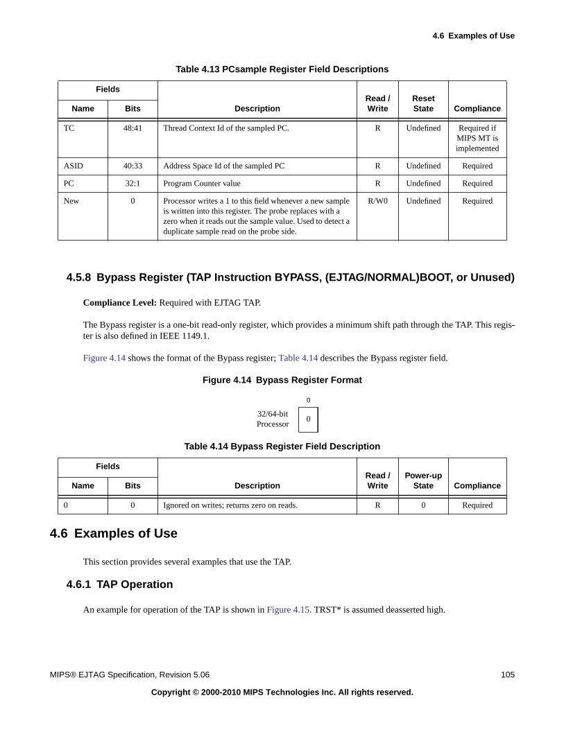
4.6 Examples of Use
MIPS® EJTAG Specification, Revision 5.06 105
Copyright © 2000-2010 MIPS Technologies Inc. All rights reserved.
4.5.8 Bypass Register (TAP Instruction BYPASS, (EJTAG/NORMAL)BOOT, or Unused)
Compliance Level: Required with EJTAG TAP.
The Bypass register is a one-bit read-only register, which provides a minimum shift path through the TAP. This regis-ter is also defined in IEEE 1149.1.
Figure 4.14 shows the format of the Bypass register; Table 4.14 describes the Bypass register field.
Figure 4.14 Bypass Register Format
4.6 Examples of Use
This section provides several examples that use the TAP.
4.6.1 TAP Operation
An example for operation of the TAP is shown in Figure 4.15. TRST* is assumed deasserted high.
Table 4.13 PCsample Register Field Descriptions
Fields
DescriptionRead /Write
ResetState ComplianceName Bits
TC 48:41 Thread Context Id of the sampled PC. R Undefined Required ifMIPS MT isimplemented
ASID 40:33 Address Space Id of the sampled PC R Undefined Required
PC 32:1 Program Counter value R Undefined Required
New 0 Processor writes a 1 to this field whenever a new sampleis written into this register. The probe replaces with azero when it reads out the sample value. Used to detect aduplicate sample read on the probe side.
R/W0 Undefined Required
0
32/64-bitProcessor
0
Table 4.14 Bypass Register Field Description
Fields
DescriptionRead /Write
Power-upState ComplianceName Bits
0 0 Ignored on writes; returns zero on reads. R 0 Required
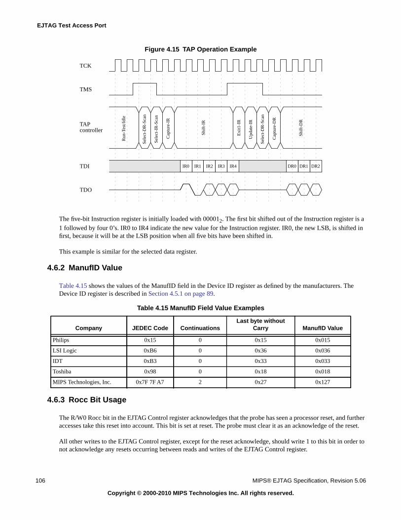
EJTAG Test Access Port
106 MIPS® EJTAG Specification, Revision 5.06
Copyright © 2000-2010 MIPS Technologies Inc. All rights reserved.
Figure 4.15 TAP Operation Example
The five-bit Instruction register is initially loaded with 000012. The first bit shifted out of the Instruction register is a1 followed by four 0’s. IR0 to IR4 indicate the new value for the Instruction register. IR0, the new LSB, is shifted infirst, because it will be at the LSB position when all five bits have been shifted in.
This example is similar for the selected data register.
4.6.2 ManufID Value
Table 4.15 shows the values of the ManufID field in the Device ID register as defined by the manufacturers. TheDevice ID register is described in Section 4.5.1 on page 89.
4.6.3 Rocc Bit Usage
The R/W0 Rocc bit in the EJTAG Control register acknowledges that the probe has seen a processor reset, and furtheraccesses take this reset into account. This bit is set at reset. The probe must clear it as an acknowledge of the reset.
All other writes to the EJTAG Control register, except for the reset acknowledge, should write 1 to this bit in order tonot acknowledge any resets occurring between reads and writes of the EJTAG Control register.
Table 4.15 ManufID Field Value Examples
Company JEDEC Code ContinuationsLast byte without
Carry ManufID Value
Philips 0x15 0 0x15 0x015
LSI Logic 0xB6 0 0x36 0x036
IDT 0xB3 0 0x33 0x033
Toshiba 0x98 0 0x18 0x018
MIPS Technologies, Inc. 0x7F 7F A7 2 0x27 0x127
Run
-Tes
t/Idl
e
TCK
Sele
ct-D
R-S
can
Cap
ture
-IR
Shif
t-IR
Exi
t1-I
R
Upd
ate-
IR
Sele
ct-D
R-S
can
Cap
ture
-DR
Shif
t-D
R
Sele
ct-I
R-S
can
TMS
TDI
TDO
TAPcontroller
IR0 IR1 IR2 IR3 IR4 DR0 DR1 DR2
4.6 Examples of Use
MIPS® EJTAG Specification, Revision 5.06 107
Copyright © 2000-2010 MIPS Technologies Inc. All rights reserved.
Correct use of the Rocc bit ensures safe handling of processor access even across reset. An example is the followingscenario:
1. A processor access is pending and the PrAcc is read with value 1 (Rocc has been cleared previously).
2. The Address and Data registers are accessed and set up to handle the processor access.
3. The EJTAG Control register is accessed to finish the processor access. The register is read in the Capture-DRstate. Shifting in of the value to write begins.
4. A reset of the processor occurs, the Rocc bit is set, and the PrAcc bit is cleared.
5. A new processor access occurs, because EJTAGBOOT was indicated.
6. A write of the EJTAG Control register is attempted with PrAcc equal to 0 and Rocc equal to 1, but the write doesnot occur because the Rocc bit is set. The new processor access that was not seen is not finished.
7. Polling of the EJTAG Control register continues. The probe detects that the Rocc bit is set.
8. The probe writes the EJTAG Control register with Rocc equal to 0 to acknowledge that the probe has seen thereset.
9. The new processor access is serviced as usual.
Inhibiting writes to the EJTAG Control register because of the Rocc bit ensures that the new processor access is notfinished by mistake due to detection of a pending processor access before the reset occurred.
4.6.4 EJTAG Memory Access Through Processor Access
The processor access feature makes it possible for the probe to handle accesses from the processors to the specificEJTAG memory area (dmseg). Thus the processor can execute a debug handler from EJTAG memory, whereby appli-cations that are not prepared with EJTAG code in the system memory still can be debugged.
The probe can get information about the access through the TAP as shown in Table 4.16.
The servicing of processor accesses works with a polling scheme, where the PrAcc bit is polled until a pending pro-cessor access is indicated by PrAcc equal to 1. Then the Address register is read to get the address of the transaction,and the Data register is accessed to get the write data or provide the read data. Finally the PrAcc bit is cleared, inorder to finish the access from the processor.
In addition, the ProbTrap and ProbEn bits control the debug exception vector location and the indication to the pro-cessor that the probe will service accesses to the EJTAG memory through processor accesses.
Table 4.16 Information Provided to Probe at Processor Access
Information Field and Register
Pending processor access PrAcc field in the EJTAG Control register
Read or write access PRnW field in the EJTAG Control register
Size and data location Psz field in EJTAG Control register, and two or three LSBs in the Address register
Address Address register
Data Data register
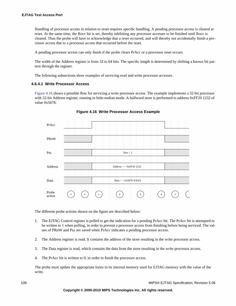
EJTAG Test Access Port
108 MIPS® EJTAG Specification, Revision 5.06
Copyright © 2000-2010 MIPS Technologies Inc. All rights reserved.
Handling of processor access in relation to reset requires specific handling. A pending processor access is cleared atreset. At the same time, the Rocc bit is set, thereby inhibiting any processor accesses to be finished until Rocc iscleared. Thus the probe will have to acknowledge that a reset occurred, and will thereby not accidentally finish a pro-cessor access due to a processor access that occurred before the reset.
A pending processor access can only finish if the probe clears PrAcc or a processor reset occurs.
The width of the Address register is from 32 to 64 bits. The specific length is determined by shifting a known bit pat-tern through the register.
The following subsections show examples of servicing read and write processor accesses.
4.6.4.1 Write Processor Access
Figure 4.16 shows a possible flow for servicing a write processor access. The example implements a 32-bit processorwith 32-bit Address register, running in little-endian mode. A halfword store is performed to address 0xFF20 1232 ofvalue 0x5678.
Figure 4.16 Write Processor Access Example
The different probe actions shown on the figure are described below:
1. The EJTAG Control register is polled to get the indication for a pending PrAcc bit. The PrAcc bit is attempted tobe written to 1 when polling, in order to prevent a processor access from finishing before being serviced. The val-ues of PRnW and Psz are saved when PrAcc indicates a pending processor access.
2. The Address register is read. It contains the address of the store resulting in the write processor access.
3. The Data register is read, which contains the data from the store resulting in the write processor access.
4. The PrAcc bit is written to 0, in order to finish the processor access.
The probe must update the appropriate bytes in its internal memory used for EJTAG memory with the value of thewrite.
PrAcc
Probeaction
PRnW
Psz
Address
Data
1 1
Data = = 0x5678 XXXX
Address = = 0xFF20 1232
Size = 1
2 3 41 1

4.6 Examples of Use
MIPS® EJTAG Specification, Revision 5.06 109
Copyright © 2000-2010 MIPS Technologies Inc. All rights reserved.
Notice that the two lower bytes of the Data register are undefined, and that the two lower bytes of the saved registerare shifted up on the two high bytes in the Data register as on a data bus for an external memory system. The Addressregister in this case contains the address from the store; however, for some accesses, this is not the case because thetwo LSBs (32-bit processor) are modified for some accesses depending on size and address.
4.6.4.2 Read Processor Access
Figure 4.17 shows a possible flow for servicing a read processor access. The example implements a 64-bit processorwith 36-bit Address register. A doubleword load/fetch from address 0xFFFF FFFF FF20 3450 is shown in the figure.
Figure 4.17 Read Processor Access Example
The different probe actions shown in the figure are described below:
1. The EJTAG Control register is polled for the indication of a pending PrAcc bit. The PrAcc bit is attempted to bewritten to 1 when polling, in order to prevent a processor access from finishing before being serviced. The valuesof PRnW and Psz are saved when PrAcc indicates a pending processor access.
2. The Address register is read. It contains the address of the load/fetch resulting in the write processor access, withthe three LSBs (64-bit processor) modified to allow size indication together with the Psz.
3. The Data register is written with the data to return for the load/fetch, resulting in the read processor access.
4. The PrAcc bit is cleared, in order to finish the processor access.
The probe must provide data for the read processor access from the internal EJTAG memory.
Notice that the Address register does not contain the direct address from the access, because the three LSBs (64-bitprocessor) are modified to indicate the size in conjunction with Psz. Also notice that in this case, there is no shiftingof the data returned for the processor access by writing to the Data register, because a doubleword is provided. Forother accesses, the Data register must be written with a shifted value depending on the specific access.
PrAcc
Probeaction
PRnW
Psz
Address
Data
1 1
Data =
Address = = 0xF FF20 3457
Size = 3
2 3 41 1
0x0..0 0..0 0..0 BEEF
EJTAG Test Access Port
110 MIPS® EJTAG Specification, Revision 5.06
Copyright © 2000-2010 MIPS Technologies Inc. All rights reserved.
Chapter 5
MIPS® EJTAG Specification, Revision 5.06 111
Copyright © 2000-2010 MIPS Technologies Inc. All rights reserved.
Hardware Breakpoints
This chapter describes the optional instruction and data hardware breakpoints. It contains the following sections:
• Section 5.1 “Introduction”
• Section 5.2 “Overview of Instruction and Data Breakpoint Registers”
• Section 5.3 “Conditions for Matching Breakpoints”
• Section 5.4 “Debug Exceptions from Breakpoints”
• Section 5.5 “Breakpoints Used as Triggerpoints”
• Section 5.6 “Instruction Breakpoint Registers”
• Section 5.7 “Data Breakpoint Registers”
• Section 5.8 “Recommendations for Implementing Hardware Breakpoints”
• Section 5.9 “Breakpoint Examples”
The general description in this chapter covers processors with R4000 privileged environments. Differences for pro-cessors with R3000 privileged environments are described in Appendix A, “Differences for R3000 PrivilegedEnvironments” on page 187.
5.1 Introduction
Hardware breakpoints compare addresses and data of executed instructions, including data load/store accesses.Instruction breakpoints can be set even on addresses in ROM areas, and data breakpoints can cause debug exceptionson specific data accesses. Instruction and data hardware breakpoints are alike in many aspects, and are described inparallel in the following sections. When the term “breakpoint” is used in this chapter, then the reference is to a “hard-ware breakpoint”, unless otherwise explicitly noted.
The breakpoints provide the following key features:
• From zero to 15 instruction breakpoints can be implemented to cause debug exceptions on executed instructions,both in ROM and RAM. Bit masking is provided for virtual address compares, and masking of compares withASID (optional) is also provided.
• From zero to 15 data breakpoints can be implemented to cause debug exceptions on data accesses. Bit masking isprovided for virtual address compares, masking of compares with ASID (optional) is provided, optional datavalue compares allows masking at byte level, and qualification on byte access and access type is possible.
• Registers for setup and control are memory mapped in the drseg segment, accessible in Debug Mode only.
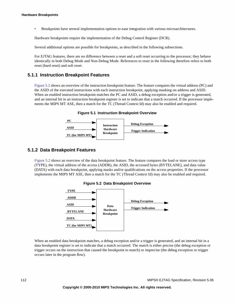
Hardware Breakpoints
112 MIPS® EJTAG Specification, Revision 5.06
Copyright © 2000-2010 MIPS Technologies Inc. All rights reserved.
• Breakpoints have several implementation options to ease integration with various microarchitectures.
Hardware breakpoints require the implementation of the Debug Control Register (DCR).
Several additional options are possible for breakpoints, as described in the following subsections.
For EJTAG features, there are no difference between a reset and a soft reset occurring to the processor; they behaveidentically in both Debug Mode and Non-Debug Mode. References to reset in the following therefore refers to bothreset (hard reset) and soft reset.
5.1.1 Instruction Breakpoint Features
Figure 5.2 shows an overview of the instruction breakpoint feature. The feature compares the virtual address (PC) andthe ASID of the executed instructions with each instruction breakpoint, applying masking on address and ASID.When an enabled instruction breakpoint matches the PC and ASID, a debug exception and/or a trigger is generated,and an internal bit in an instruction breakpoint register is set to indicate that a match occurred. If the processor imple-ments the MIPS MT ASE, then a match for the TC (Thread Context Id) may also be enabled and required.
Figure 5.1 Instruction Breakpoint Overview
5.1.2 Data Breakpoint Features
Figure 5.2 shows an overview of the data breakpoint feature. The feature compares the load or store access type(TYPE), the virtual address of the access (ADDR), the ASID, the accessed bytes (BYTELANE), and data value(DATA) with each data breakpoint, applying masks and/or qualifications on the access properties. If the processorimplements the MIPS MT ASE, then a match for the TC (Thread Context Id) may also be enabled and required.
Figure 5.2 Data Breakpoint Overview
When an enabled data breakpoint matches, a debug exception and/or a trigger is generated, and an internal bit in adata breakpoint register is set to indicate that a match occurred. The match is either precise (the debug exception ortrigger occurs on the instruction that caused the breakpoint to match) or imprecise (the debug exception or triggeroccurs later in the program flow).
InstructionHardwareBreakpoint
Debug Exception
Trigger IndicationASID
PC
TC (for MIPS MT)
DataHardwareBreakpoint
TYPE
ASIDDebug Exception
Trigger Indication
ADDR
DATA
BYTELANE
TC (for MIPS MT)
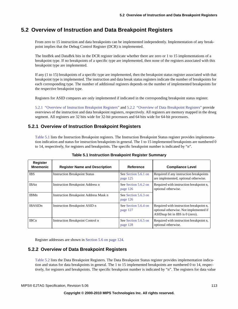
5.2 Overview of Instruction and Data Breakpoint Registers
MIPS® EJTAG Specification, Revision 5.06 113
Copyright © 2000-2010 MIPS Technologies Inc. All rights reserved.
5.2 Overview of Instruction and Data Breakpoint Registers
From zero to 15 instruction and data breakpoints can be implemented independently. Implementation of any break-point implies that the Debug Control Register (DCR) is implemented.
The InstBrk and DataBrk bits in the DCR register indicate whether there are zero or 1 to 15 implementations of abreakpoint type. If no breakpoints of a specific type are implemented, then none of the registers associated with thisbreakpoint type are implemented.
If any (1 to 15) breakpoints of a specific type are implemented, then the breakpoint status register associated with thatbreakpoint type is implemented. The instruction and data break status registers indicate the number of breakpoints foreach corresponding type. The number of additional registers depends on the number of implemented breakpoints forthe respective breakpoint type.
Registers for ASID compares are only implemented if indicated in the corresponding breakpoint status register.
5.2.1 “Overview of Instruction Breakpoint Registers” and 5.2.2 “Overview of Data Breakpoint Registers” provideoverviews of the instruction and data breakpoint registers, respectively. All registers are memory mapped in the drsegsegment. All registers are 32 bits wide for 32-bit processors and 64 bits wide for 64-bit processors.
5.2.1 Overview of Instruction Breakpoint Registers
Table 5.1 lists the Instruction Breakpoint registers. The Instruction Breakpoint Status register provides implementa-tion indication and status for instruction breakpoints in general. The 1 to 15 implemented breakpoints are numbered 0to 14, respectively, for registers and breakpoints. The specific breakpoint number is indicated by “n”.
Register addresses are shown in Section 5.6 on page 124.
5.2.2 Overview of Data Breakpoint Registers
Table 5.2 lists the Data Breakpoint Registers. The Data Breakpoint Status register provides implementation indica-tion and status for data breakpoints in general. The 1 to 15 implemented breakpoints are numbered 0 to 14, respec-tively, for registers and breakpoints. The specific breakpoint number is indicated by “n”. The registers for data value
Table 5.1 Instruction Breakpoint Register Summary
RegisterMnemonic Register Name and Description Reference Compliance Level
IBS Instruction Breakpoint Status See Section 5.6.1 onpage 125
Required if any instruction breakpointsare implemented, optional otherwise.
IBAn Instruction Breakpoint Address n See Section 5.6.2 onpage 126
Required with instruction breakpoint n,optional otherwise.
IBMn Instruction Breakpoint Address Mask n See Section 5.6.3 onpage 126
IBASIDn Instruction Breakpoint ASID n See Section 5.6.4 onpage 127
Required with instruction breakpoint n,optional otherwise. Not implemented ifASIDsup bit in IBS is 0 (zero).
IBCn Instruction Breakpoint Control n See Section 5.6.5 onpage 128
Required with instruction breakpoint n,optional otherwise.
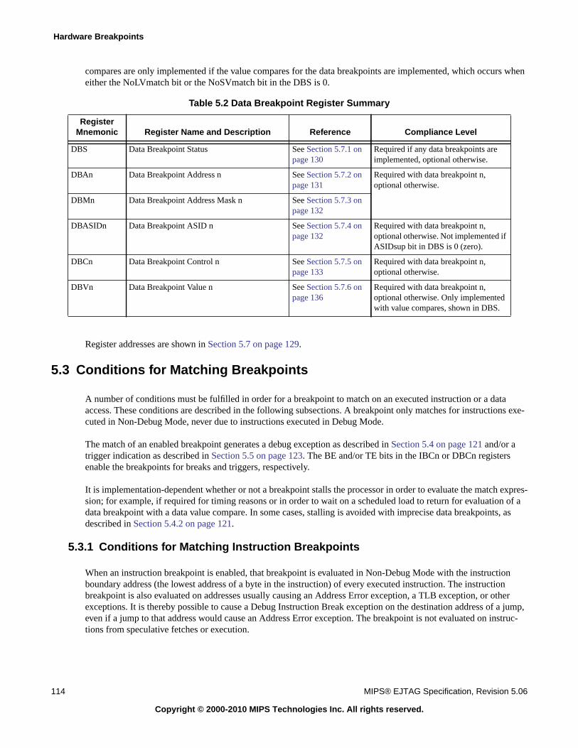
Hardware Breakpoints
114 MIPS® EJTAG Specification, Revision 5.06
Copyright © 2000-2010 MIPS Technologies Inc. All rights reserved.
compares are only implemented if the value compares for the data breakpoints are implemented, which occurs wheneither the NoLVmatch bit or the NoSVmatch bit in the DBS is 0.
Register addresses are shown in Section 5.7 on page 129.
5.3 Conditions for Matching Breakpoints
A number of conditions must be fulfilled in order for a breakpoint to match on an executed instruction or a dataaccess. These conditions are described in the following subsections. A breakpoint only matches for instructions exe-cuted in Non-Debug Mode, never due to instructions executed in Debug Mode.
The match of an enabled breakpoint generates a debug exception as described in Section 5.4 on page 121 and/or atrigger indication as described in Section 5.5 on page 123. The BE and/or TE bits in the IBCn or DBCn registersenable the breakpoints for breaks and triggers, respectively.
It is implementation-dependent whether or not a breakpoint stalls the processor in order to evaluate the match expres-sion; for example, if required for timing reasons or in order to wait on a scheduled load to return for evaluation of adata breakpoint with a data value compare. In some cases, stalling is avoided with imprecise data breakpoints, asdescribed in Section 5.4.2 on page 121.
5.3.1 Conditions for Matching Instruction Breakpoints
When an instruction breakpoint is enabled, that breakpoint is evaluated in Non-Debug Mode with the instructionboundary address (the lowest address of a byte in the instruction) of every executed instruction. The instructionbreakpoint is also evaluated on addresses usually causing an Address Error exception, a TLB exception, or otherexceptions. It is thereby possible to cause a Debug Instruction Break exception on the destination address of a jump,even if a jump to that address would cause an Address Error exception. The breakpoint is not evaluated on instruc-tions from speculative fetches or execution.
Table 5.2 Data Breakpoint Register Summary
RegisterMnemonic Register Name and Description Reference Compliance Level
DBS Data Breakpoint Status See Section 5.7.1 onpage 130
Required if any data breakpoints areimplemented, optional otherwise.
DBAn Data Breakpoint Address n See Section 5.7.2 onpage 131
Required with data breakpoint n,optional otherwise.
DBMn Data Breakpoint Address Mask n See Section 5.7.3 onpage 132
DBASIDn Data Breakpoint ASID n See Section 5.7.4 onpage 132
Required with data breakpoint n,optional otherwise. Not implemented ifASIDsup bit in DBS is 0 (zero).
DBCn Data Breakpoint Control n See Section 5.7.5 onpage 133
Required with data breakpoint n,optional otherwise.
DBVn Data Breakpoint Value n See Section 5.7.6 onpage 136
Required with data breakpoint n,optional otherwise. Only implementedwith value compares, shown in DBS.
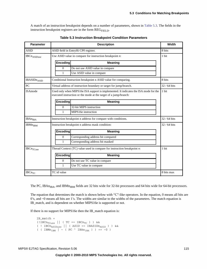
5.3 Conditions for Matching Breakpoints
MIPS® EJTAG Specification, Revision 5.06 115
Copyright © 2000-2010 MIPS Technologies Inc. All rights reserved.
A match of an instruction breakpoint depends on a number of parameters, shown in Table 5.3. The fields in theinstruction breakpoint registers are in the form REGFIELD.
The PC, IBAnIBA, and IBMnIBM fields are 32 bits wide for 32-bit processors and 64 bits wide for 64-bit processors.
The equation that determines the match is shown below with “C”-like operators. In the equation, 0 means all bits are0’s, and ~0 means all bits are 1’s. The widths are similar to the widths of the parameters. The match equation isIB_match, and is dependent on whether MIPS16e is supported or not.
If there is no support for MIPS16e then the IB_match equation is:
IB_match =(!IBCnTCuse || ( TC == IBCnTC ) ) &&( ! IBCnASIDuse || ( ASID == IBASIDnASID ) ) &&( ( IBMnIBM | ~ ( PC ^ IBAnIBA ) ) == ~0 )
Table 5.3 Instruction Breakpoint Condition Parameters
Parameter Description Width
ASID ASID field in EntryHi CP0 register. 8 bits
IBCnASIDuse Use ASID value in compare for instruction breakpoint n: 1 bit
IBASIDnASID Conditional Instruction breakpoint n ASID value for comparing. 8 bits
PC Virtual address of instruction boundary or target for jump/branch. 32 / 64 bits
ISAmode Used only when MIPS16e ISA support is implemented. It indicates the ISA mode for theexecuted instruction or the mode at the target of a jump/branch:
1 bit
IBAnIBA Instruction breakpoint n address for compare with conditions. 32 / 64 bits
IBMnIBM Instruction breakpoint n address mask condition: 32 / 64 bits
IBCnTCuse Thread Context (TC) value used in compare for instruction breakpoint n: 1 bit
IBCnTC TC id value 8 bits max
Encoding Meaning
0 Do not use ASID value in compare
1 Use ASID value in compare
Encoding Meaning
0 32-bit MIPS instruction
1 MIPS16e instruction
Encoding Meaning
0 Corresponding address bit compared
1 Corresponding address bit masked
Encoding Meaning
0 Do not use TC value in compare
1 Use TC value in compare
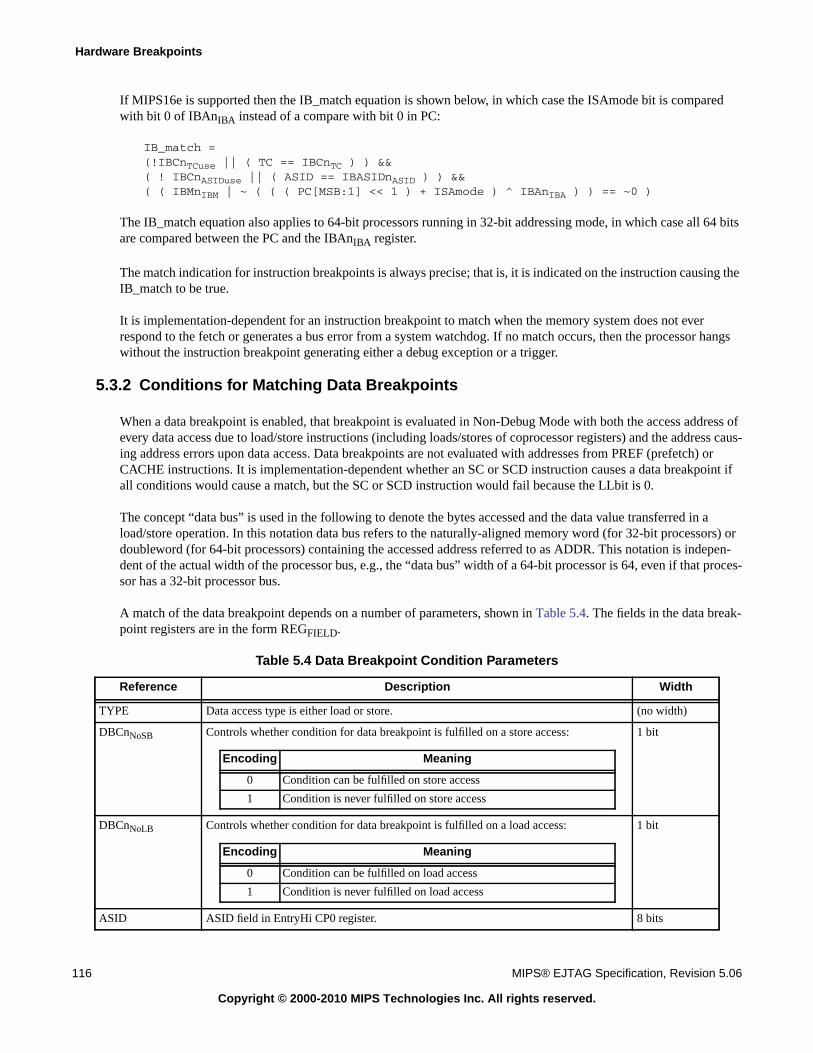
Hardware Breakpoints
116 MIPS® EJTAG Specification, Revision 5.06
Copyright © 2000-2010 MIPS Technologies Inc. All rights reserved.
If MIPS16e is supported then the IB_match equation is shown below, in which case the ISAmode bit is comparedwith bit 0 of IBAnIBA instead of a compare with bit 0 in PC:
IB_match =(!IBCnTCuse || ( TC == IBCnTC ) ) &&( ! IBCnASIDuse || ( ASID == IBASIDnASID ) ) &&( ( IBMnIBM | ~ ( ( ( PC[MSB:1] << 1 ) + ISAmode ) ^ IBAnIBA ) ) == ~0 )
The IB_match equation also applies to 64-bit processors running in 32-bit addressing mode, in which case all 64 bitsare compared between the PC and the IBAnIBA register.
The match indication for instruction breakpoints is always precise; that is, it is indicated on the instruction causing theIB_match to be true.
It is implementation-dependent for an instruction breakpoint to match when the memory system does not everrespond to the fetch or generates a bus error from a system watchdog. If no match occurs, then the processor hangswithout the instruction breakpoint generating either a debug exception or a trigger.
5.3.2 Conditions for Matching Data Breakpoints
When a data breakpoint is enabled, that breakpoint is evaluated in Non-Debug Mode with both the access address ofevery data access due to load/store instructions (including loads/stores of coprocessor registers) and the address caus-ing address errors upon data access. Data breakpoints are not evaluated with addresses from PREF (prefetch) orCACHE instructions. It is implementation-dependent whether an SC or SCD instruction causes a data breakpoint ifall conditions would cause a match, but the SC or SCD instruction would fail because the LLbit is 0.
The concept “data bus” is used in the following to denote the bytes accessed and the data value transferred in aload/store operation. In this notation data bus refers to the naturally-aligned memory word (for 32-bit processors) ordoubleword (for 64-bit processors) containing the accessed address referred to as ADDR. This notation is indepen-dent of the actual width of the processor bus, e.g., the “data bus” width of a 64-bit processor is 64, even if that proces-sor has a 32-bit processor bus.
A match of the data breakpoint depends on a number of parameters, shown in Table 5.4. The fields in the data break-point registers are in the form REGFIELD.
Table 5.4 Data Breakpoint Condition Parameters
Reference Description Width
TYPE Data access type is either load or store. (no width)
DBCnNoSB Controls whether condition for data breakpoint is fulfilled on a store access: 1 bit
DBCnNoLB Controls whether condition for data breakpoint is fulfilled on a load access: 1 bit
ASID ASID field in EntryHi CP0 register. 8 bits
Encoding Meaning
0 Condition can be fulfilled on store access
1 Condition is never fulfilled on store access
Encoding Meaning
0 Condition can be fulfilled on load access
1 Condition is never fulfilled on load access
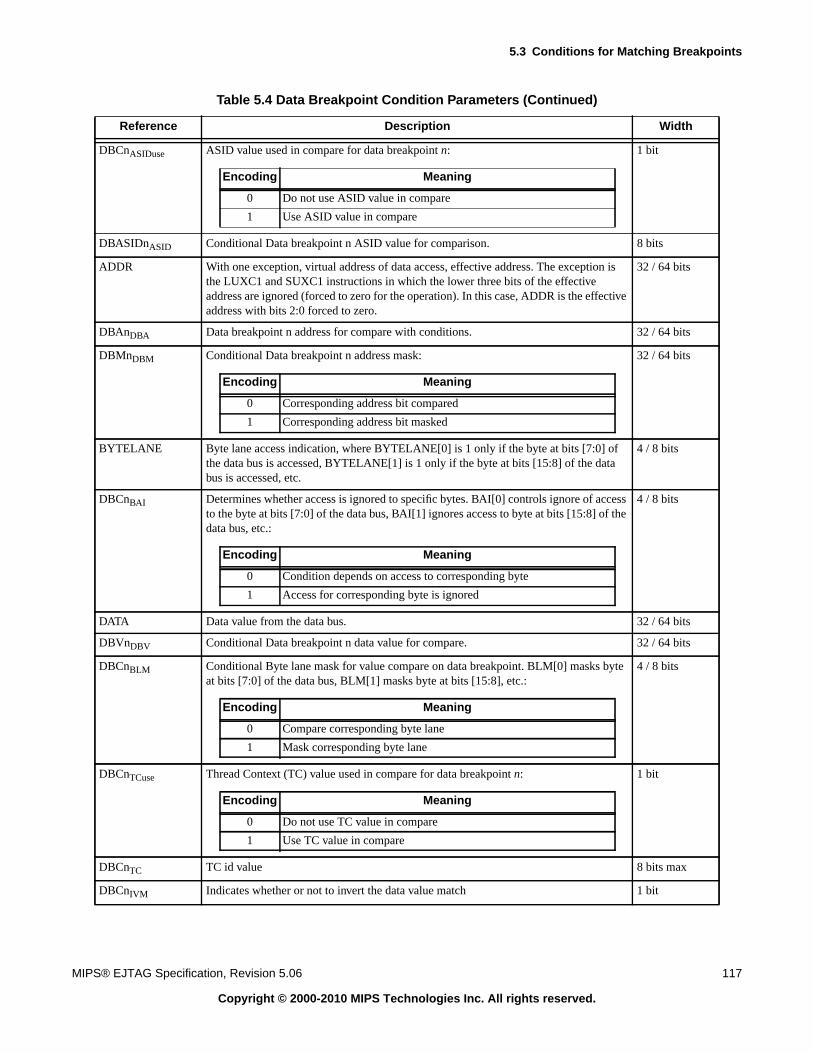
5.3 Conditions for Matching Breakpoints
MIPS® EJTAG Specification, Revision 5.06 117
Copyright © 2000-2010 MIPS Technologies Inc. All rights reserved.
DBCnASIDuse ASID value used in compare for data breakpoint n: 1 bit
DBASIDnASID Conditional Data breakpoint n ASID value for comparison. 8 bits
ADDR With one exception, virtual address of data access, effective address. The exception isthe LUXC1 and SUXC1 instructions in which the lower three bits of the effectiveaddress are ignored (forced to zero for the operation). In this case, ADDR is the effectiveaddress with bits 2:0 forced to zero.
32 / 64 bits
DBAnDBA Data breakpoint n address for compare with conditions. 32 / 64 bits
DBMnDBM Conditional Data breakpoint n address mask: 32 / 64 bits
BYTELANE Byte lane access indication, where BYTELANE[0] is 1 only if the byte at bits [7:0] ofthe data bus is accessed, BYTELANE[1] is 1 only if the byte at bits [15:8] of the databus is accessed, etc.
4 / 8 bits
DBCnBAI Determines whether access is ignored to specific bytes. BAI[0] controls ignore of accessto the byte at bits [7:0] of the data bus, BAI[1] ignores access to byte at bits [15:8] of thedata bus, etc.:
4 / 8 bits
DATA Data value from the data bus. 32 / 64 bits
DBVnDBV Conditional Data breakpoint n data value for compare. 32 / 64 bits
DBCnBLM Conditional Byte lane mask for value compare on data breakpoint. BLM[0] masks byteat bits [7:0] of the data bus, BLM[1] masks byte at bits [15:8], etc.:
4 / 8 bits
DBCnTCuse Thread Context (TC) value used in compare for data breakpoint n: 1 bit
DBCnTC TC id value 8 bits max
DBCnIVM Indicates whether or not to invert the data value match 1 bit
Table 5.4 Data Breakpoint Condition Parameters (Continued)
Reference Description Width
Encoding Meaning
0 Do not use ASID value in compare
1 Use ASID value in compare
Encoding Meaning
0 Corresponding address bit compared
1 Corresponding address bit masked
Encoding Meaning
0 Condition depends on access to corresponding byte
1 Access for corresponding byte is ignored
Encoding Meaning
0 Compare corresponding byte lane
1 Mask corresponding byte lane
Encoding Meaning
0 Do not use TC value in compare
1 Use TC value in compare
Hardware Breakpoints
118 MIPS® EJTAG Specification, Revision 5.06
Copyright © 2000-2010 MIPS Technologies Inc. All rights reserved.
The ADDR, DBAnDBA, DBMnDBM, DATA, and DBVnDBV fields are 32 bits wide for 32-bit processors and 64 bitswide for 64-bit processors. The BYTELANE, DBCnBLM, and DBCnBAI fields are four bits wide for 32-bit proces-sors and eight bits wide for 64-bit processors. The width is indicated as “N” in the equations below.
The match equations are shown below with “C”-like operators. In the equation, 0 means all bits are 0’s, and ~0 meansall bits are 1’s. The bit widths are similar to the widths of the parameters.
DB_match is the overall match equation (the DB_addr_match, DB_no_value_compare, and DB_value_match equa-tions in the DB_match equation are defined below):
DB_match =(!DBCnTCuse || ( TC == DBCnTC ) ) &&( ( ( TYPE == load ) && ! DBCnNoLB ) || ( ( TYPE == store ) && ! DBCnNoSB ) ) &&DB_addr_match && ( DB_no_value_compare || DB_value_match )
DB_addr_match is defined as:
DB_addr_match =( ! DBCnASIDuse || ( ASID == DBASIDnASID ) ) &&( ( DBMnDBM | ~ ( ADDR ^ DBAnDBA ) ) == ~0 ) &&( ( ~ DBCnBAI & BYTELANE ) != 0 )
The DB_addr_match equation also applies to 64-bit processors running in 32-bit addressing mode, in which case all64 bits are compared between the ADDR and the DBAnDBA field. Please note the special case used for ADDR for theLUXC1 and SUXC1 instructions as described in Table 5.4.
DB_no_value_compare is defined as:
DB_no_value_compare =( ( DBCnBLM | DBCnBAI | ~ BYTELANE ) == ~0 )
If a data value compare is indicated on a breakpoint, then DB_no_value_compare is false, and if there is no data valuecompare then DB_no_value_compare is true. Note that a data value compare is a run-time property of the breakpointif (DBCnBLM | DBCnBAI) is not ~0, because DB_no_value_compare then depends on BYTELANE provided by theload/store instructions. The DBCIVM bit inverts the sense of the match. If set, the value match term will be high if thedata value is not the same as the data in the DBVn register.
If a data value compare is required, then the data value from the data bus is compared and masked with the registersfor the data breakpoint, as shown in the DB_value_match equation:
DB_value_match =DBCnIVM ^( ( DATA[7:0] == DBVnDBV[7:0] ) || ! BYTELANE[0] || DBCnBLM[0] || DBCnBAI[0] ) &&( ( DATA[15:8] == DBVnDBV[15:8] ) || ! BYTELANE[1] || DBCnBLM[1] || DBCnBAI[1] ) &&......( ( DATA[8*N-1:8*N-8] == DBVnDBV[8*N-1:8*N-8] ) ||
! BYTELANE[N-1] || DBCnBLM[N-1] || DBCnBAI[N-1] )
Data breakpoints depend on endianess, because values on the byte lanes are used in the equations. Thus it is requiredthat the debug software programs the breakpoints accordingly to endianess.
It is implementation-dependent for a data breakpoint to match when the memory system does not ever respond to thedata access or generates a bus error from a system watchdog. If no match occurs, then the processor hangs without thedata breakpoint generating a debug exception or trigger.
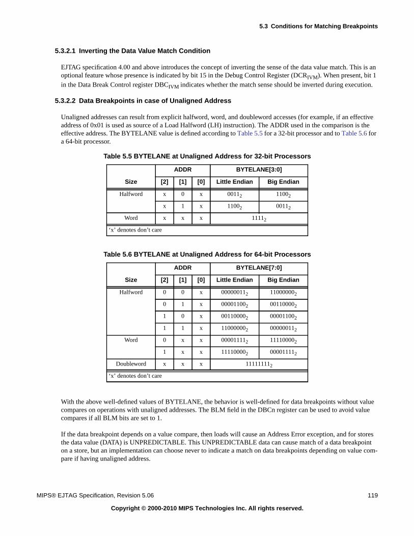
5.3 Conditions for Matching Breakpoints
MIPS® EJTAG Specification, Revision 5.06 119
Copyright © 2000-2010 MIPS Technologies Inc. All rights reserved.
5.3.2.1 Inverting the Data Value Match Condition
EJTAG specification 4.00 and above introduces the concept of inverting the sense of the data value match. This is anoptional feature whose presence is indicated by bit 15 in the Debug Control Register (DCRIVM). When present, bit 1in the Data Break Control register DBCIVM indicates whether the match sense should be inverted during execution.
5.3.2.2 Data Breakpoints in case of Unaligned Address
Unaligned addresses can result from explicit halfword, word, and doubleword accesses (for example, if an effectiveaddress of 0x01 is used as source of a Load Halfword (LH) instruction). The ADDR used in the comparison is theeffective address. The BYTELANE value is defined according to Table 5.5 for a 32-bit processor and to Table 5.6 fora 64-bit processor.
With the above well-defined values of BYTELANE, the behavior is well-defined for data breakpoints without valuecompares on operations with unaligned addresses. The BLM field in the DBCn register can be used to avoid valuecompares if all BLM bits are set to 1.
If the data breakpoint depends on a value compare, then loads will cause an Address Error exception, and for storesthe data value (DATA) is UNPREDICTABLE. This UNPREDICTABLE data can cause match of a data breakpointon a store, but an implementation can choose never to indicate a match on data breakpoints depending on value com-pare if having unaligned address.
Table 5.5 BYTELANE at Unaligned Address for 32-bit Processors
Size
ADDR BYTELANE[3:0]
[2] [1] [0] Little Endian Big Endian
Halfword x 0 x 00112 11002
x 1 x 11002 00112
Word x x x 11112
‘x’ denotes don’t care
Table 5.6 BYTELANE at Unaligned Address for 64-bit Processors
Size
ADDR BYTELANE[7:0]
[2] [1] [0] Little Endian Big Endian
Halfword 0 0 x 000000112 110000002
0 1 x 000011002 001100002
1 0 x 001100002 000011002
1 1 x 110000002 000000112
Word 0 x x 000011112 111100002
1 x x 111100002 000011112
Doubleword x x x 111111112
‘x’ denotes don’t care
Hardware Breakpoints
120 MIPS® EJTAG Specification, Revision 5.06
Copyright © 2000-2010 MIPS Technologies Inc. All rights reserved.
If a debug exception is taken on the store then the debug handler can investigate the processor state and thereby deter-mine if the address was unaligned and UNPREDICTABLE store data for the memory access thereby caused thedebug exception. If a debug exception is not taken for the store, then an Address Error exception is taken. So, in bothcases it is possible for debug software to detect the bug. The BLM field in the DBCn register can be used to avoidcompare on UNPREDICTABLE data, in case all of the BLM bits are set to 1.
If the data breakpoint is used as a triggerpoint (see Section 5.5 on page 123) then a Break Status (BS) bit might be setafter a compare with UNPREDICTABLE data; however, an Address Error exception occurs in this case thereby mak-ing it possible to detect the bug.
5.3.2.3 Match for Data Breakpoint with Value Compare on Bus or Cache Error
If a data value compare is required to evaluate a data breakpoint, the DB_no_value_compare equation is false (seeSection 5.3.2 on page 116). However, if a bus or cache error occurs on the load, then there is no valid data to use inthe compare. This case has two possibilities:
• The match will fail.
• The match will compare on invalid data, and then indicate a pending bus or cache error through the DBusEP orCacheEP bits in the Debug register, if a debug exception is taken. This occurrence might cause a trigger indica-tion to be set on the compare with invalid data.
A bus or cache error on a store does not affect the data breakpoint compare.
Refer to Section 5.8.3 on page 137 for recommendations on implementing data breakpoint compares on invalid data.
5.3.2.4 Precise Match for Data Breakpoints
A precise match for a data breakpoint occurs when the match equation can be fully evaluated at the time theload/store instruction is executed. A true DB_match can thereby be indicated on the very same instruction causing theDB_match equation to be true.
Matches on data breakpoints without data value compares are always precise. Accesses using data value comparesare either imprecise or precise depending on the implementation and specific access.
5.3.2.5 Imprecise Match for Data Breakpoints
An imprecise match for a data breakpoint occurs when the match equation cannot be fully evaluated at the time theload/store instruction is executed. This case occurs when the processor is not stalled on a scheduled load and a databreakpoint must compare on the data value returned by the load. If the breakpoint matches, then the DB_match equa-tion is true later in the execution flow rather than at the same time as load/store instruction that caused the load/storeaccess to match.
Only data breakpoints with value compares can be imprecise, in which case the breakpoints can be imprecise for allor some of those accesses depending on the implementation.
5.3.3 Precise Exceptions on Data Value Match Breaks
When the EJTAG hardware implements data value match breaks to be taken precisely, the core EJTAG hardware onobtaining the data value will match the value and cause an exception to be taken on the load instruction. In this situa-tion, the data value is already read out from its source location and brought to the processor. When the exception han-dler has taken the exception, the DEPC points to the load instruction (because the exception is taken precisely), andthe load instruction reexecutes on a return from exception. If the load value was being read from regular memory,
5.4 Debug Exceptions from Breakpoints
MIPS® EJTAG Specification, Revision 5.06 121
Copyright © 2000-2010 MIPS Technologies Inc. All rights reserved.
then this is usually not an issue. But in a situation where the load data was coming from a special FIFO or I/O regis-ter, this instruction cannot be re-executed without altering the state of the peripheral or special memory. To handlethis type of situation, when the EJTAG hardware implements precise data value exceptions, it is also expected to keepthe load data value in a drseg register. This allows the debug exception handler to re-execute this instruction in soft-ware using this data value. The debug handler must also re-calculate the new DEPC value and update it before exe-cuting the DERET instruction. This Load Data Value register is at drseg address 0x2FF0.
This is an optional feature of regular EJTAG introduced in revision 4.00 and above, and the presence of this feature isindicated by bit 14 (DVM) of the DCR register.
5.4 Debug Exceptions from Breakpoints
This section describes how to set up instruction and data breakpoints to generate debug exceptions when the matchconditions are true.
5.4.1 Debug Exception Caused by Instruction Breakpoint
The BE bit in the IBCn register must be set for an instruction breakpoint to be enabled. A Debug Instruction Breakexception occurs when the IB_match equation is true (see Section 5.3.1 on page 114). The corresponding Break Sta-tus (BS) bit in the IBS register is set when the breakpoint generates the debug exception. Note that the BE bit aloneenables the break point exception, whether or not the TE bit is set (see Section 5.5 on page 123).
The Debug Instruction Break exception is precise, so the DEPC register and DBD bit in the Debug register (seeSection 2.7 on page 55) point to the instruction that caused the IB_match equation to be true.
The instruction receiving the debug exception only updates the debug related registers. That instruction will not causeany loads/stores to occur. Thus a debug exception from a data breakpoint cannot occur at the same time an instructionreceives a Debug Instruction Break exception.
The debug handler usually returns to the instruction causing the Debug Instruction Break exception, whereby theinstruction is executed. Debug software must disable the breakpoint when returning to the instruction; otherwise, theDebug Instruction Break exception will reoccur. An alternative is for debug software to emulate the instruction(s) insoftware and change the DEPC accordingly.
5.4.2 Debug Exception by Data Breakpoint
The BE bit in the DBCn register must be set for a data breakpoint to be enabled. A debug exception occurs when theDB_match condition is true (see Section 5.3.2 on page 116). A matching data breakpoint generates either a precise oran imprecise debug exception. Note that the BE bit alone enables the break point exception, whether or not the TE bitis set (see Section 5.5 “Breakpoints Used as Triggerpoints”).
Refer to Section 5.8.4 on page 137 for additional information on precise and imprecise debug exceptions.
5.4.2.1 Debug Data Break Load/Store Exception as a Precise Debug Exception
A Debug Data Break Load/Store exception occurs when a data breakpoint indicates a precise match. In this case, theDEPC register and DBD bit in the Debug register point to the load/store instruction that caused the DB_match equa-
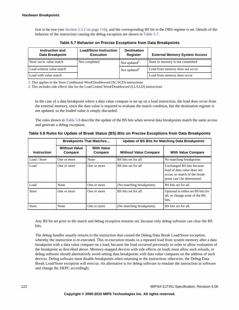
Hardware Breakpoints
122 MIPS® EJTAG Specification, Revision 5.06
Copyright © 2000-2010 MIPS Technologies Inc. All rights reserved.
tion to be true (see Section 5.3.2 on page 116), and the corresponding BS bit in the DBS register is set. Details of thebehavior of the instruction causing the debug exception are shown in Table 5.7.
In the case of a data breakpoint where a data value compare is set up on a load instruction, the load does occur fromthe external memory, since the data value is required to evaluate the match condition, but the destination register isnot updated, so the loaded value is simply discarded.
The rules shown in Table 5.8 describe the update of the BS bits when several data breakpoints match the same accessand generate a debug exception.
Any BS bit set prior to the match and debug exception remains set, because only debug software can clear the BSbits.
The debug handler usually returns to the instruction that caused the Debug Data Break Load/Store exception,whereby the instruction is re-executed. This re-execution results in a repeated load from system memory after a databreakpoint with a data value compare on a load, because the load occurred previously in order to allow evaluation ofthe breakpoint as described above. Memory-mapped devices with side effects on loads must allow such reloads, ordebug software should alternatively avoid setting data breakpoints with data value compares on the address of suchdevices. Debug software must disable breakpoints when returning to the instruction; otherwise, the Debug DataBreak Load/Store exception will reoccur. An alternative is for debug software to emulate the instruction in softwareand change the DEPC accordingly.
Table 5.7 Behavior on Precise Exceptions from Data Breakpoints
Instruction andData Breakpoint
Load/Store InstructionExecution
DestinationRegister External Memory System Access
Store wo/w value match Not completed Not updated1
1. This applies to the Store Conditional Word/Doubleword (SC/SCD) instructions
Store to memory is not committed
Load without value match Not updated2
2. This includes side effects like for the Load Linked Word/Doubleword (LL/LLD) instructions
Load from memory does not occur
Load with value match Load from memory does occur
Table 5.8 Rules for Update of Break Status (BS) Bits on Precise Exceptions from Data Breakpoints
Instruction
Breakpoints That Matches... Update of BS Bits for Matching Data Breakpoints
Without ValueCompare
With ValueCompare Without Value Compare With Value Compare
Load / Store One or more None BS bits set for all No matching breakpoints
Load One or more One or more BS bits set for all Unchanged BS bits becauseload of data value does notoccur, so match of the break-point can’t be determined.
Load None One or more (No matching breakpoints) BS bits set for all.
Store One or more One or more BS bits set for all Optional to either set BS bits forall, or change none of the BSbits.
Store None One or more (No matching breakpoints) BS bits set for all.
5.5 Breakpoints Used as Triggerpoints
MIPS® EJTAG Specification, Revision 5.06 123
Copyright © 2000-2010 MIPS Technologies Inc. All rights reserved.
5.4.2.2 Debug Data Break Load/Store Exception as an Imprecise Debug Exception
A Debug Data Break Load/Store Imprecise exception occurs when a data breakpoint indicates an imprecise match. Inthis case, the DEPC register and DBD bit in the Debug register point to an instruction later in the execution flowrather than at the load/store instruction that caused the DB_match equation to be true.
The load/store instruction causing the Debug Data Break Load/Store Imprecise exception always updates the destina-tion register and completes the access to the external memory system. Therefore this load/store instruction is notre-executed on return from the debug handler, because the DEPC register and DBD bit do not point to that instruc-tion.
Several imprecise data breakpoints can be pending at a given time, if the bus system supports multiple outstandingdata accesses. The breakpoints are evaluated as the accesses finalize, and a Debug Data Break Load/Store Impreciseexception is generated only for the first one matching. Both the first and succeeding matches cause corresponding BSbits and DDBLImpr/DDBSImpr to be set, but no debug exception is generated for succeeding matches because theprocessor is already in Debug Mode. Similarly, if a debug exception had already occurred at the time of the firstmatch (for example, due to a precise debug exception), then all matches cause the corresponding BS bits andDDBLImpr/DDBSImpr to be set, but no debug exception is generated because the processor is already in DebugMode.
The SYNC and EHB instructions, followed by appropriate spacing, (as described in Section 2.2.3.7 on page 38 andSection 2.2.4 on page 39) must be executed before the BS bits and DDBLImpr/DDBSImpr bits are respectivelyaccessed for read or write. This delay ensures that these bits are fully updated.
Any BS bit set prior to the match and debug exception are kept set, because only debug software can clear the BSbits.
5.5 Breakpoints Used as Triggerpoints
Software can set up both instruction and data breakpoints such that a matching breakpoint does not generate a debugexception, but sends an indication through the BS bit only. But note that if the BE bit is set, then a debug exceptionwill be generated, even if the TE bit is set. The TE bit in the IBCn or DBCn register controls whether an instruction ordata breakpoint, respectively, is used as a triggerpoint. Triggerpoints are evaluated for matches under the same crite-ria as breakpoints.
The BS bit in the IBS or DBS register is set for a triggerpoint when the respective IB_match condition (see Section5.3.1 on page 114) or DB_match condition (see Section 5.3.2 on page 116) is true.
For the BS bit to be set for an instruction triggerpoint, either the instruction must be fully executed or an exceptionmust occur on the instruction.
Table 5.9 Actions Resulting from an Instruction/Data Match for Specified BE and TE Bit Values
TE BE Breakpoint Exception BS bit is set in IBS/DBS
0 0 Not taken No
0 1 Taken Yes
1 0 Not taken Yes
1 1 Taken Yes
Hardware Breakpoints
124 MIPS® EJTAG Specification, Revision 5.06
Copyright © 2000-2010 MIPS Technologies Inc. All rights reserved.
The BS bit for a data triggerpoint can only be set if no exception with higher priority than the Debug Data BreakLoad/Store exception with address match only occurred on the load/store instruction. For exceptions with equal orlower priority than the Debug Data Break Load/Store exception with address match only, the BS bits are still set for amatching triggerpoint. For example, the BS bit is set even if a TLB or Bus Error exception occurred on the load/storeinstruction. Data triggerpoints with value compares require the data value to be valid for the BS bit to be set, which isnot the case if, for example, a TLB or Bus Error exception occurs on a load instruction. However, for stores, the trig-ger may compare on UNPREDICTABLE data as described in Section 5.3.2.2 on page 119.
The rules for update of the BS bits are shown in Table 5.10.
Data breakpoints with imprecise matches generate imprecise triggers when enabled by the TE bit.
Note that trigger indications by BS may be set based on compare with UNPREDICTABLE data, as described in (seeSection 5.3.2.2 on page 119).
A triggerpoint match can be indicated on an optional internal signal or chip pin.
5.6 Instruction Breakpoint Registers
This section describes the instruction breakpoint registers for MIPS32 and MIPS64 processors, and other R4000 priv-ileged environment implementations of 32-bit and 64-bit processors. These registers provide status and control forthe instruction breakpoints. All registers are in the drseg segment. The 1 to 15 implemented breakpoints are numbered0 to 14, respectively, for registers and breakpoints. The specific breakpoint number is indicated by “n” in the range 0to 15 depending on the implemented number of instruction breakpoints. The registers and their respective addressesoffsets are shown in Table 5.11. For a description of the two registers IBCC and IBPC used for complex breakpoints,see Section 6.3.2 on page 145 and Section 6.3.4 on page 147 respectively.
Table 5.10 Rules for Update of Break Status (BS) Bits on Data Triggerpoints
Instruction Without/With Value Compare BS Bits Update for Triggerpoint
Load / Store Without value compare BS bit set if no exception with higher priority than the DebugData Break Load/Store exception, with address match only,occurred on the instruction.
Load With value compare BS bit set if no exception with higher priority than the DebugData Break Load exception, with address and data value match,occurred on the instruction.
Store With value compare BS bit is set if no exception occurred on the instruction, and isoptional to be if an exception with equal or lower priority than theDebug Data Break Store exception, with address match only,occurred on the instruction, with the requirement that either all therelevant BS bits are set, or none are changed.
Table 5.11 Instruction Breakpoint Register Mapping
Offset in drsegRegister
Mnemonic Register Name and Description
0x1000 IBS Instruction Breakpoint Status
0x1100 + 0x100 * n IBAn Instruction Breakpoint Address n
0x1108 + 0x100 * n IBMn Instruction Breakpoint Address Mask n
0x1110 + 0x100 * n IBASIDn Instruction Breakpoint ASID n
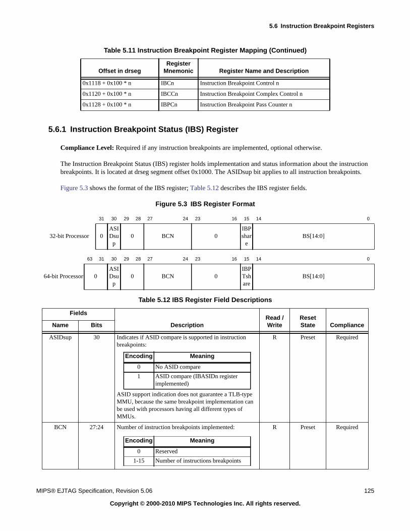
5.6 Instruction Breakpoint Registers
MIPS® EJTAG Specification, Revision 5.06 125
Copyright © 2000-2010 MIPS Technologies Inc. All rights reserved.
5.6.1 Instruction Breakpoint Status (IBS) Register
Compliance Level: Required if any instruction breakpoints are implemented, optional otherwise.
The Instruction Breakpoint Status (IBS) register holds implementation and status information about the instructionbreakpoints. It is located at drseg segment offset 0x1000. The ASIDsup bit applies to all instruction breakpoints.
Figure 5.3 shows the format of the IBS register; Table 5.12 describes the IBS register fields.
Figure 5.3 IBS Register Format
0x1118 + 0x100 * n IBCn Instruction Breakpoint Control n
0x1120 + 0x100 * n IBCCn Instruction Breakpoint Complex Control n
0x1128 + 0x100 * n IBPCn Instruction Breakpoint Pass Counter n
31 30 29 28 27 24 23 16 15 14 0
32-bit Processor 0ASIDsu
p0 BCN 0
IBPshar
eBS[14:0]
63 31 30 29 28 27 24 23 16 15 14 0
64-bit Processor 0ASIDsu
p0 BCN 0
IBPTshare
BS[14:0]
Table 5.12 IBS Register Field Descriptions
Fields
DescriptionRead /Write
ResetState ComplianceName Bits
ASIDsup 30 Indicates if ASID compare is supported in instructionbreakpoints:
ASID support indication does not guarantee a TLB-typeMMU, because the same breakpoint implementation canbe used with processors having all different types ofMMUs.
R Preset Required
BCN 27:24 Number of instruction breakpoints implemented: R Preset Required
Table 5.11 Instruction Breakpoint Register Mapping (Continued)
Offset in drsegRegister
Mnemonic Register Name and Description
Encoding Meaning
0 No ASID compare
1 ASID compare (IBASIDn registerimplemented)
Encoding Meaning
0 Reserved
1-15 Number of instructions breakpoints
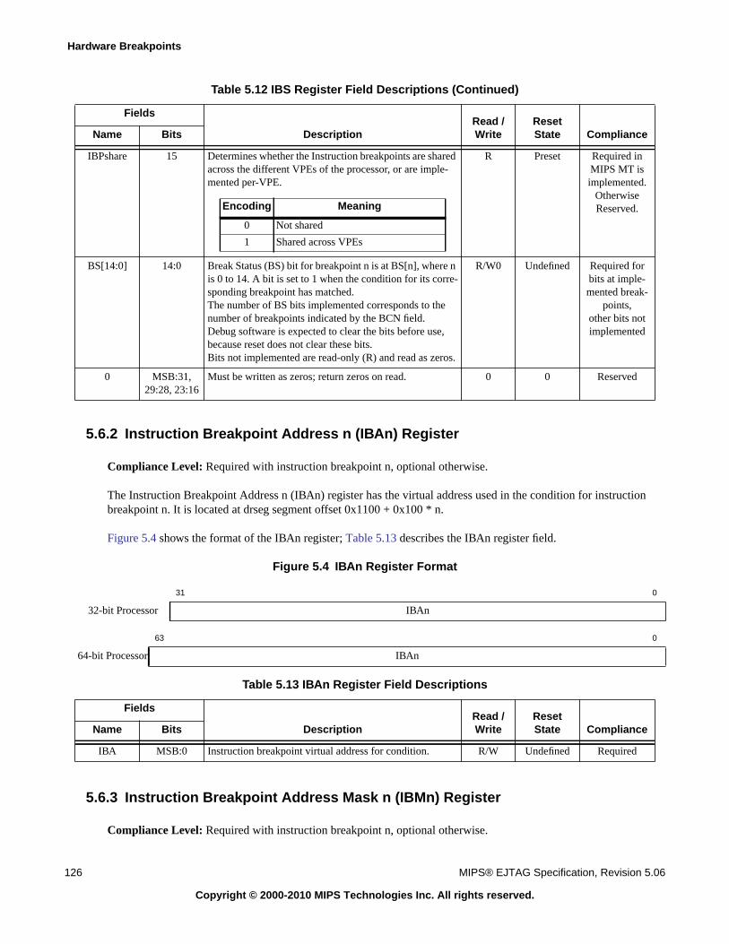
Hardware Breakpoints
126 MIPS® EJTAG Specification, Revision 5.06
Copyright © 2000-2010 MIPS Technologies Inc. All rights reserved.
5.6.2 Instruction Breakpoint Address n (IBAn) Register
Compliance Level: Required with instruction breakpoint n, optional otherwise.
The Instruction Breakpoint Address n (IBAn) register has the virtual address used in the condition for instructionbreakpoint n. It is located at drseg segment offset 0x1100 + 0x100 * n.
Figure 5.4 shows the format of the IBAn register; Table 5.13 describes the IBAn register field.
Figure 5.4 IBAn Register Format
5.6.3 Instruction Breakpoint Address Mask n (IBMn) Register
Compliance Level: Required with instruction breakpoint n, optional otherwise.
IBPshare 15 Determines whether the Instruction breakpoints are sharedacross the different VPEs of the processor, or are imple-mented per-VPE.
R Preset Required inMIPS MT isimplemented.
OtherwiseReserved.
BS[14:0] 14:0 Break Status (BS) bit for breakpoint n is at BS[n], where nis 0 to 14. A bit is set to 1 when the condition for its corre-sponding breakpoint has matched.The number of BS bits implemented corresponds to thenumber of breakpoints indicated by the BCN field.Debug software is expected to clear the bits before use,because reset does not clear these bits.Bits not implemented are read-only (R) and read as zeros.
R/W0 Undefined Required forbits at imple-mented break-
points,other bits notimplemented
0 MSB:31,29:28, 23:16
Must be written as zeros; return zeros on read. 0 0 Reserved
31 0
32-bit Processor IBAn
63 0
64-bit Processor IBAn
Table 5.13 IBAn Register Field Descriptions
Fields
DescriptionRead /Write
ResetState ComplianceName Bits
IBA MSB:0 Instruction breakpoint virtual address for condition. R/W Undefined Required
Table 5.12 IBS Register Field Descriptions (Continued)
Fields
DescriptionRead /Write
ResetState ComplianceName Bits
Encoding Meaning
0 Not shared
1 Shared across VPEs
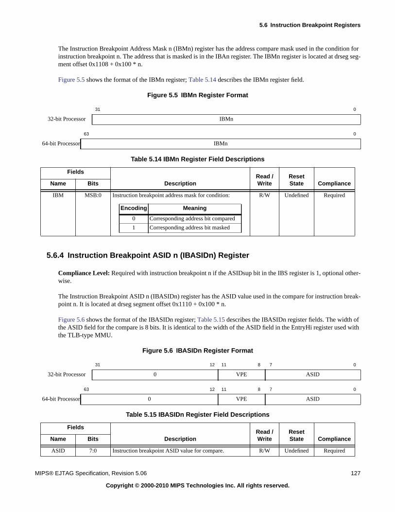
5.6 Instruction Breakpoint Registers
MIPS® EJTAG Specification, Revision 5.06 127
Copyright © 2000-2010 MIPS Technologies Inc. All rights reserved.
The Instruction Breakpoint Address Mask n (IBMn) register has the address compare mask used in the condition forinstruction breakpoint n. The address that is masked is in the IBAn register. The IBMn register is located at drseg seg-ment offset 0x1108 + 0x100 * n.
Figure 5.5 shows the format of the IBMn register; Table 5.14 describes the IBMn register field.
Figure 5.5 IBMn Register Format
5.6.4 Instruction Breakpoint ASID n (IBASIDn) Register
Compliance Level: Required with instruction breakpoint n if the ASIDsup bit in the IBS register is 1, optional other-wise.
The Instruction Breakpoint ASID n (IBASIDn) register has the ASID value used in the compare for instruction break-point n. It is located at drseg segment offset 0x1110 + 0x100 * n.
Figure 5.6 shows the format of the IBASIDn register; Table 5.15 describes the IBASIDn register fields. The width ofthe ASID field for the compare is 8 bits. It is identical to the width of the ASID field in the EntryHi register used withthe TLB-type MMU.
Figure 5.6 IBASIDn Register Format
31 0
32-bit Processor IBMn
63 0
64-bit Processor IBMn
Table 5.14 IBMn Register Field Descriptions
Fields
DescriptionRead /Write
ResetState ComplianceName Bits
IBM MSB:0 Instruction breakpoint address mask for condition: R/W Undefined Required
31 12 11 8 7 0
32-bit Processor 0 VPE ASID
63 12 11 8 7 0
64-bit Processor 0 VPE ASID
Table 5.15 IBASIDn Register Field Descriptions
Fields
DescriptionRead /Write
ResetState ComplianceName Bits
ASID 7:0 Instruction breakpoint ASID value for compare. R/W Undefined Required
Encoding Meaning
0 Corresponding address bit compared
1 Corresponding address bit masked
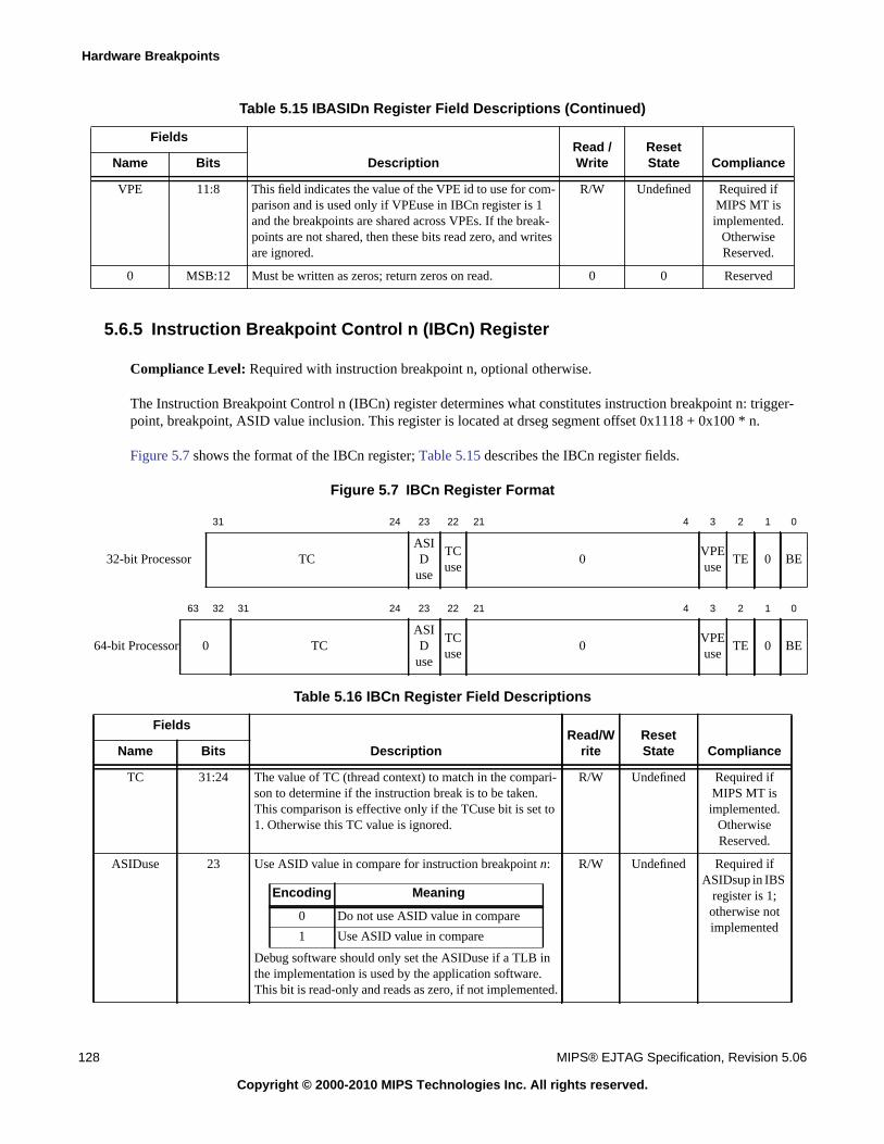
Hardware Breakpoints
128 MIPS® EJTAG Specification, Revision 5.06
Copyright © 2000-2010 MIPS Technologies Inc. All rights reserved.
5.6.5 Instruction Breakpoint Control n (IBCn) Register
Compliance Level: Required with instruction breakpoint n, optional otherwise.
The Instruction Breakpoint Control n (IBCn) register determines what constitutes instruction breakpoint n: trigger-point, breakpoint, ASID value inclusion. This register is located at drseg segment offset 0x1118 + 0x100 * n.
Figure 5.7 shows the format of the IBCn register; Table 5.15 describes the IBCn register fields.
Figure 5.7 IBCn Register Format
VPE 11:8 This field indicates the value of the VPE id to use for com-parison and is used only if VPEuse in IBCn register is 1and the breakpoints are shared across VPEs. If the break-points are not shared, then these bits read zero, and writesare ignored.
R/W Undefined Required ifMIPS MT isimplemented.
OtherwiseReserved.
0 MSB:12 Must be written as zeros; return zeros on read. 0 0 Reserved
31 24 23 22 21 4 3 2 1 0
32-bit Processor TCASID
use
TCuse
0VPEuse
TE 0 BE
63 32 31 24 23 22 21 4 3 2 1 0
64-bit Processor 0 TCASID
use
TCuse
0VPEuse
TE 0 BE
Table 5.16 IBCn Register Field Descriptions
Fields
DescriptionRead/W
riteResetState ComplianceName Bits
TC 31:24 The value of TC (thread context) to match in the compari-son to determine if the instruction break is to be taken.This comparison is effective only if the TCuse bit is set to1. Otherwise this TC value is ignored.
R/W Undefined Required ifMIPS MT isimplemented.
OtherwiseReserved.
ASIDuse 23 Use ASID value in compare for instruction breakpoint n:
Debug software should only set the ASIDuse if a TLB inthe implementation is used by the application software.This bit is read-only and reads as zero, if not implemented.
R/W Undefined Required ifASIDsup in IBS
register is 1;otherwise notimplemented
Table 5.15 IBASIDn Register Field Descriptions (Continued)
Fields
DescriptionRead /Write
ResetState ComplianceName Bits
Encoding Meaning
0 Do not use ASID value in compare
1 Use ASID value in compare
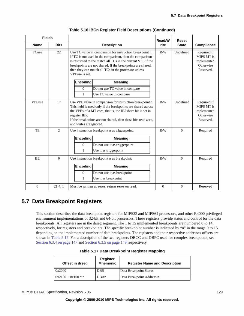
5.7 Data Breakpoint Registers
MIPS® EJTAG Specification, Revision 5.06 129
Copyright © 2000-2010 MIPS Technologies Inc. All rights reserved.
5.7 Data Breakpoint Registers
This section describes the data breakpoint registers for MIPS32 and MIPS64 processors, and other R4000 privilegedenvironment implementations of 32-bit and 64-bit processors. These registers provide status and control for the databreakpoints. All registers are in the drseg segment. The 1 to 15 implemented breakpoints are numbered 0 to 14,respectively, for registers and breakpoints. The specific breakpoint number is indicated by “n” in the range 0 to 15depending on the implemented number of data breakpoints. The registers and their respective addresses offsets areshown in Table 5.17. For a description of the two registers DBCC and DBPC used for complex breakpoints, seeSection 6.3.4 on page 147 and Section 6.3.5 on page 149 respectively.
TCuse 22 Use TC value in comparison for instruction breakpoint n.If TC is not used in the comparison, then the comparisonis restricted to the match all TCs in the current VPE if thebreakpoints are not shared. If the breakpoints are shared,then they can match all TCs in the processor unlessVPEuse is set.
R/W Undefined Required ifMIPS MT isimplemented.
OtherwiseReserved.
VPEuse 17 Use VPE value in comparison for instruction breakpoint n.This field is used only if the breakpoints are shared acrossthe VPEs of a MT core, that is, the IBPshare bit is set inregister IBP.If the breakpoints are not shared, then these bits read zero,and writes are ignored.
R/W Undefined Required ifMIPS MT isimplemented.
OtherwiseReserved.
TE 2 Use instruction breakpoint n as triggerpoint: R/W 0 Required
BE 0 Use instruction breakpoint n as breakpoint: R/W 0 Required
0 21:4, 1 Must be written as zeros; return zeros on read. 0 0 Reserved
Table 5.17 Data Breakpoint Register Mapping
Offset in drsegRegister
Mnemonic Register Name and Description
0x2000 DBS Data Breakpoint Status
0x2100 + 0x100 * n DBAn Data Breakpoint Address n
Table 5.16 IBCn Register Field Descriptions (Continued)
Fields
DescriptionRead/W
riteResetState ComplianceName Bits
Encoding Meaning
0 Do not use TC value in compare
1 Use TC value in compare
Encoding Meaning
0 Do not use it as triggerpoint
1 Use it as triggerpoint
Encoding Meaning
0 Do not use it as breakpoint
1 Use it as breakpoint
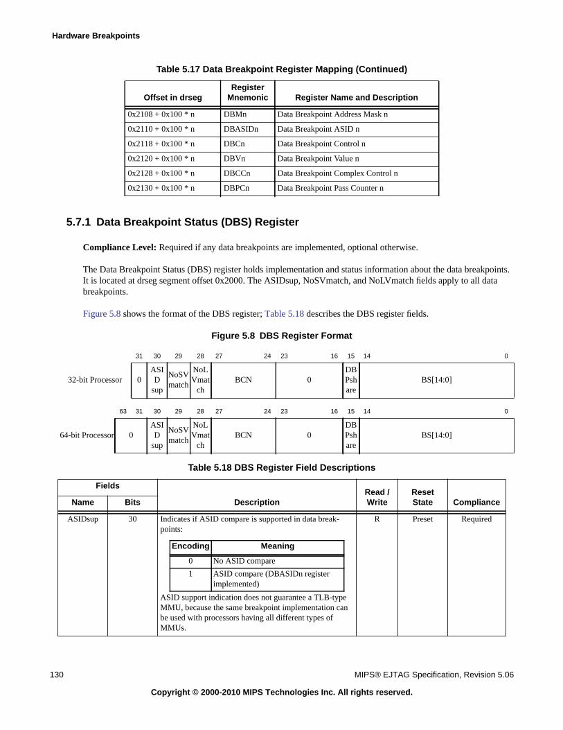
Hardware Breakpoints
130 MIPS® EJTAG Specification, Revision 5.06
Copyright © 2000-2010 MIPS Technologies Inc. All rights reserved.
5.7.1 Data Breakpoint Status (DBS) Register
Compliance Level: Required if any data breakpoints are implemented, optional otherwise.
The Data Breakpoint Status (DBS) register holds implementation and status information about the data breakpoints.It is located at drseg segment offset 0x2000. The ASIDsup, NoSVmatch, and NoLVmatch fields apply to all databreakpoints.
Figure 5.8 shows the format of the DBS register; Table 5.18 describes the DBS register fields.
Figure 5.8 DBS Register Format
0x2108 + 0x100 * n DBMn Data Breakpoint Address Mask n
0x2110 + 0x100 * n DBASIDn Data Breakpoint ASID n
0x2118 + 0x100 * n DBCn Data Breakpoint Control n
0x2120 + 0x100 * n DBVn Data Breakpoint Value n
0x2128 + 0x100 * n DBCCn Data Breakpoint Complex Control n
0x2130 + 0x100 * n DBPCn Data Breakpoint Pass Counter n
31 30 29 28 27 24 23 16 15 14 0
32-bit Processor 0ASID
sup
NoSVmatch
NoLVmat
chBCN 0
DBPshare
BS[14:0]
63 31 30 29 28 27 24 23 16 15 14 0
64-bit Processor 0ASID
sup
NoSVmatch
NoLVmat
chBCN 0
DBPshare
BS[14:0]
Table 5.18 DBS Register Field Descriptions
Fields
DescriptionRead /Write
ResetState ComplianceName Bits
ASIDsup 30 Indicates if ASID compare is supported in data break-points:
ASID support indication does not guarantee a TLB-typeMMU, because the same breakpoint implementation canbe used with processors having all different types ofMMUs.
R Preset Required
Table 5.17 Data Breakpoint Register Mapping (Continued)
Offset in drsegRegister
Mnemonic Register Name and Description
Encoding Meaning
0 No ASID compare
1 ASID compare (DBASIDn registerimplemented)
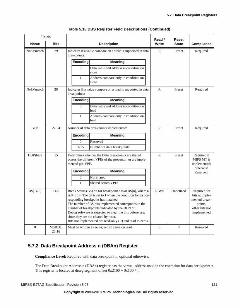
5.7 Data Breakpoint Registers
MIPS® EJTAG Specification, Revision 5.06 131
Copyright © 2000-2010 MIPS Technologies Inc. All rights reserved.
5.7.2 Data Breakpoint Address n (DBAn) Register
Compliance Level: Required with data breakpoint n, optional otherwise.
The Data Breakpoint Address n (DBAn) register has the virtual address used in the condition for data breakpoint n.This register is located at drseg segment offset 0x2100 + 0x100 * n.
NoSVmatch 29 Indicates if a value compare on a store is supported in databreakpoints:
R Preset Required
NoLVmatch 28 Indicates if a value compare on a load is supported in databreakpoints:
R Preset Required
BCN 27:24 Number of data breakpoints implemented: R Preset Required
DBPshare 15 Determines whether the Data breakpoints are sharedacross the different VPEs of the processor, or are imple-mented per-VPE.
R Preset Required ifMIPS MT isimplemented;
otherwiseReserved.
BS[14:0] 14:0 Break Status (BS) bit for breakpoint n is at BS[n], where nis 0 to 14. The bit is set to 1 when the condition for its cor-responding breakpoint has matched.The number of BS bits implemented corresponds to thenumber of breakpoints indicated by the BCN bit.Debug software is expected to clear the bits before use,since they are not cleared by reset.Bits not implemented are read-only (R) and read as zeros.
R/W0 Undefined Required forbits at imple-mented break-
points,other bits notimplemented
0 MSB:31,23:16
Must be written as zeros; return zeros on read. 0 0 Reserved
Table 5.18 DBS Register Field Descriptions (Continued)
Fields
DescriptionRead /Write
ResetState ComplianceName Bits
Encoding Meaning
0 Data value and address in condition onstore
1 Address compare only in condition onstore
Encoding Meaning
0 Data value and address in condition onload
1 Address compare only in condition onload
Encoding Meaning
0 Reserved
1-15 Number of data breakpoints
Encoding Meaning
0 Not shared
1 Shared across VPEs
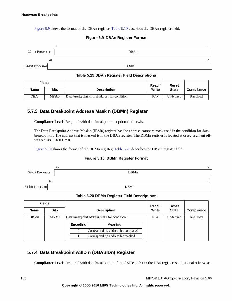
Hardware Breakpoints
132 MIPS® EJTAG Specification, Revision 5.06
Copyright © 2000-2010 MIPS Technologies Inc. All rights reserved.
Figure 5.9 shows the format of the DBAn register; Table 5.19 describes the DBAn register field.
Figure 5.9 DBAn Register Format
5.7.3 Data Breakpoint Address Mask n (DBMn) Register
Compliance Level: Required with data breakpoint n, optional otherwise.
The Data Breakpoint Address Mask n (IBMn) register has the address compare mask used in the condition for databreakpoint n. The address that is masked is in the DBAn register. The DBMn register is located at drseg segment off-set 0x2108 + 0x100 * n.
Figure 5.10 shows the format of the DBMn register; Table 5.20 describes the DBMn register field.
Figure 5.10 DBMn Register Format
5.7.4 Data Breakpoint ASID n (DBASIDn) Register
Compliance Level: Required with data breakpoint n if the ASIDsup bit in the DBS register is 1, optional otherwise.
31 0
32-bit Processor DBAn
63 0
64-bit Processor DBAn
Table 5.19 DBAn Register Field Descriptions
Fields
DescriptionRead /Write
ResetState ComplianceName Bits
DBA MSB:0 Data breakpoint virtual address for condition R/W Undefined Required
31 0
32-bit Processor DBMn
63 0
64-bit Processor DBMn
Table 5.20 DBMn Register Field Descriptions
Fields
DescriptionRead /Write
ResetState ComplianceName Bits
DBMn MSB:0 Data breakpoint address mask for condition: R/W Undefined Required
Encoding Meaning
0 Corresponding address bit compared
1 Corresponding address bit masked
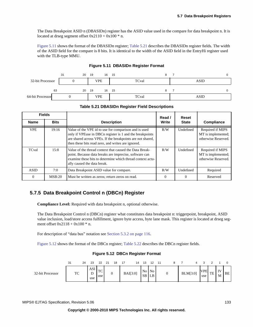
5.7 Data Breakpoint Registers
MIPS® EJTAG Specification, Revision 5.06 133
Copyright © 2000-2010 MIPS Technologies Inc. All rights reserved.
The Data Breakpoint ASID n (DBASIDn) register has the ASID value used in the compare for data breakpoint n. It islocated at drseg segment offset 0x2110 + 0x100 * n.
Figure 5.11 shows the format of the DBASIDn register; Table 5.21 describes the DBASIDn register fields. The widthof the ASID field for the compare is 8 bits. It is identical to the width of the ASID field in the EntryHi register usedwith the TLB-type MMU.
Figure 5.11 DBASIDn Register Format
5.7.5 Data Breakpoint Control n (DBCn) Register
Compliance Level: Required with data breakpoint n, optional otherwise.
The Data Breakpoint Control n (DBCn) register what constitutes data breakpoint n: triggerpoint, breakpoint, ASIDvalue inclusion, load/store access fulfillment, ignore byte access, byte lane mask. This register is located at drseg seg-ment offset 0x2118 + 0x100 * n.
For description of “data bus” notation see Section 5.3.2 on page 116.
Figure 5.12 shows the format of the DBCn register; Table 5.22 describes the DBCn register fields.
Figure 5.12 DBCn Register Format
31 20 19 16 15 8 7 0
32-bit Processor 0 VPE TCval ASID
63 20 19 16 15 8 7 0
64-bit Processor 0 VPE TCval ASID
Table 5.21 DBASIDn Register Field Descriptions
Fields
DescriptionRead /Write
ResetState ComplianceName Bits
VPE 19:16 Value of the VPE id to use for comparison and is usedonly if VPEuse in DBCn register is 1 and the breakpointsare shared across VPEs. If the breakpoints are not shared,then these bits read zero, and writes are ignored.
R/W Undefined Required if MIPSMT is implemented;otherwise Reserved.
TCval 15:8 Value of the thread context that caused the Data Break-point. Because data breaks are imprecise, software canexamine these bits to determine which thread context actu-ally caused the data break.
R/W Undefined Required if MIPSMT is implemented;otherwise Reserved.
ASID 7:0 Data Breakpoint ASID value for compare. R/W Undefined Required
0 MSB:20 Must be written as zeros; return zeros on read. 0 0 Reserved
31 24 23 22 21 18 17 14 13 12 11 8 7 4 3 2 1 0
32-bit Processor TCASID
use
TCuse
0 BAI[3:0]NoSB
NoLB
0 BLM[3:0]VPEuse
TEIVM
BE
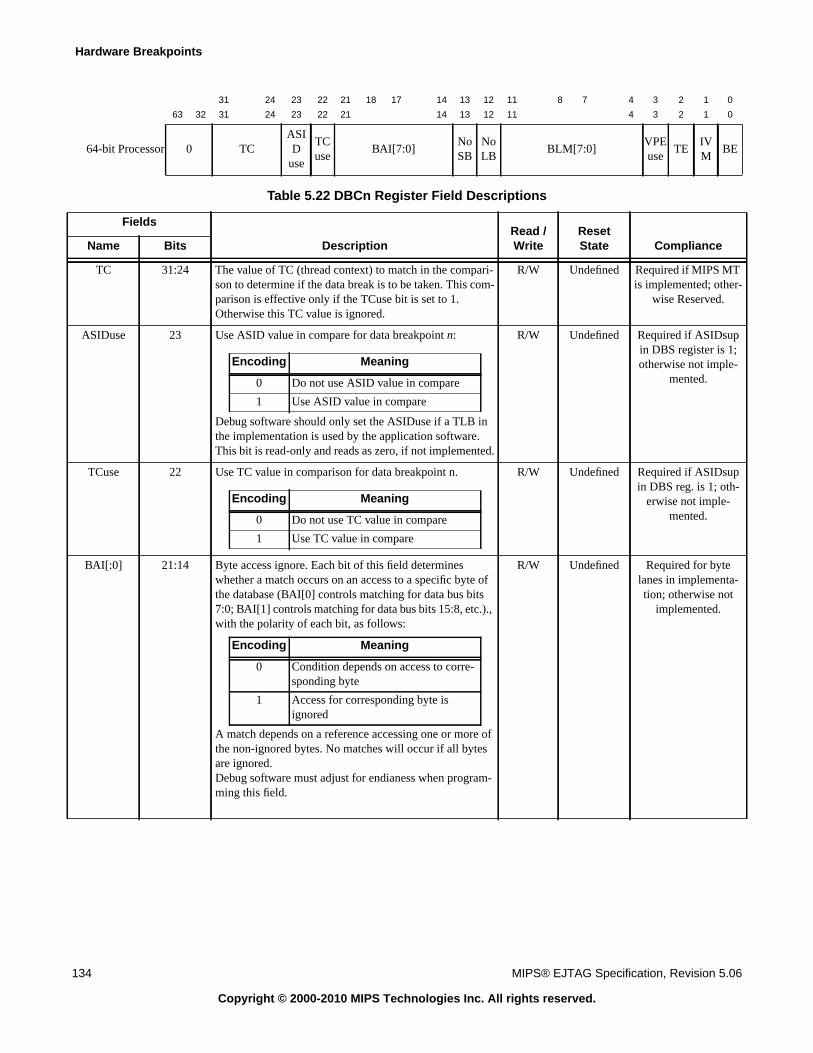
Hardware Breakpoints
134 MIPS® EJTAG Specification, Revision 5.06
Copyright © 2000-2010 MIPS Technologies Inc. All rights reserved.
63 32 31 24 23 22 21 14 13 12 11 4 3 2 1 0
64-bit Processor 0 TCASID
use
TCuse
BAI[7:0]NoSB
NoLB
BLM[7:0]VPEuse
TEIVM
BE
Table 5.22 DBCn Register Field Descriptions
Fields
DescriptionRead /Write
ResetState ComplianceName Bits
TC 31:24 The value of TC (thread context) to match in the compari-son to determine if the data break is to be taken. This com-parison is effective only if the TCuse bit is set to 1.Otherwise this TC value is ignored.
R/W Undefined Required if MIPS MTis implemented; other-
wise Reserved.
ASIDuse 23 Use ASID value in compare for data breakpoint n:
Debug software should only set the ASIDuse if a TLB inthe implementation is used by the application software.This bit is read-only and reads as zero, if not implemented.
R/W Undefined Required if ASIDsupin DBS register is 1;otherwise not imple-
mented.
TCuse 22 Use TC value in comparison for data breakpoint n. R/W Undefined Required if ASIDsupin DBS reg. is 1; oth-
erwise not imple-mented.
BAI[:0] 21:14 Byte access ignore. Each bit of this field determineswhether a match occurs on an access to a specific byte ofthe database (BAI[0] controls matching for data bus bits7:0; BAI[1] controls matching for data bus bits 15:8, etc.).,with the polarity of each bit, as follows:
A match depends on a reference accessing one or more ofthe non-ignored bytes. No matches will occur if all bytesare ignored.Debug software must adjust for endianess when program-ming this field.
R/W Undefined Required for bytelanes in implementa-tion; otherwise not
implemented.
31 24 23 22 21 18 17 14 13 12 11 8 7 4 3 2 1 0
Encoding Meaning
0 Do not use ASID value in compare
1 Use ASID value in compare
Encoding Meaning
0 Do not use TC value in compare
1 Use TC value in compare
Encoding Meaning
0 Condition depends on access to corre-sponding byte
1 Access for corresponding byte isignored
5.7 Data Breakpoint Registers
MIPS® EJTAG Specification, Revision 5.06 135
Copyright © 2000-2010 MIPS Technologies Inc. All rights reserved.
NoSB 13 Controls whether condition for data breakpoint is ever ful-filled on a store access:
R/W Undefined Required
NoLB 12 Controls whether condition for data breakpoint is ever ful-filled on a load access:
R/W Undefined Required
BLM[:0] 11:4 Byte lane mask for value compare on data breakpoint.BLM[0] masks byte at bits [7:0] of the data bus, BLM[1]masks byte at bits [15:8], etc.:
Debug software must adjust for endianess when program-ming this field. BLM[:0] are unimplemented if value compare is notimplemented, which is the case when NoSVmatch andNoLVmatch bits in DBS are both 1. Bits are read-only (R)and read as zeros if not implemented.
R/W Undefined Required for bytelanes in implementa-tion and if value com-
pare; otherwise notimplemented.
VPEuse 3 Use VPE value in comparison for instruction breakpoint n.This field is used only if the breakpoints are shared acrossthe VPEs of a MT core, that is, the DBPshare bit is set inregister DBP.If the breakpoints are not shared, this bit reads zero andwrites are ignored.
R/W Undefined Required if MIPS MTis implemented. Oth-
erwise Reserved.
TE 2 Use data breakpoint n as triggerpoint: R/W 0 Required
IVM 1 Used to indicate that the data value match should beinverted.
R/W Undefined Required if DCRIVM
is 1; otherwise notimplemented. Revi-sion 4.00 and above.
Table 5.22 DBCn Register Field Descriptions (Continued)
Fields
DescriptionRead /Write
ResetState ComplianceName Bits
Encoding Meaning
0 Condition can be fulfilled on storeaccess
1 Condition is never fulfilled on storeaccess
Encoding Meaning
0 Condition can be fulfilled on loadaccess
1 Condition is never fulfilled on loadaccess
Encoding Meaning
0 Compare corresponding byte lane
1 Mask corresponding byte lane
Encoding Meaning
0 Do not use it as triggerpoint
1 Use it as triggerpoint
Hardware Breakpoints
136 MIPS® EJTAG Specification, Revision 5.06
Copyright © 2000-2010 MIPS Technologies Inc. All rights reserved.
5.7.6 Data Breakpoint Value n (DBVn) Register
Compliance Level: Required with data breakpoint n if data value compare is supported (indicated by either NoSV-match or NoLVmatch bits in DBS being 0), optional otherwise.
The Data Breakpoint Value n (DBVn) register has the value used in the condition for data breakpoint n. It is locatedat drseg segment offset 0x2120 + 0x100 * n.
Figure 5.13 shows the format of the DBVn register; Table 5.23 describes the DBVn register field.
Figure 5.13 DBVn Register Format
5.8 Recommendations for Implementing Hardware Breakpoints
This section provides useful information for implementing instruction and data breakpoints.
5.8.1 Number of Instruction Breakpoints Without Single Stepping
If hardware single stepping is not implemented, then at least two instruction breakpoints are required. Four instruc-tion hardware breakpoints are recommended.
BE 0 Use data breakpoint n as breakpoint: R/W 0 Required
0 3 Must be written as zeros; return zeros on read. 0 0 Reserved
31 0
32-bit Processor DBVn
63 0
64-bit Processor DBVn
Table 5.23 DBVn Register Field Descriptions
Fields
DescriptionRead /Write
ResetState ComplianceName Bits
DBV MSB:0 Data breakpoint data value for condition.Debug software must adjust for endianess when program-ming this field.
R/W Undefined Required
Table 5.22 DBCn Register Field Descriptions (Continued)
Fields
DescriptionRead /Write
ResetState ComplianceName Bits
Encoding Meaning
0 Do not use it as breakpoint
1 Use it as breakpoint
5.9 Breakpoint Examples
MIPS® EJTAG Specification, Revision 5.06 137
Copyright © 2000-2010 MIPS Technologies Inc. All rights reserved.
5.8.2 Data Breakpoints with Data Value Compares
Data breakpoints should be implemented with data value compares. Also, data value compares should be imple-mented even if it is not possible to break on loads with precise data value compares. Refer to Section 5.8.4 onpage 137 for more information on precise exceptions.
5.8.3 Data Breakpoint Compare on Invalid Data
Data breakpoints should only compare on valid data, so that debug exceptions are only generated on valid data. Forexample, no debug exception should be generated for a bus error on a load that has a pending data compare break-point on the data returned by the load. This also applies to compares on store data for a store to an unaligned address.
However, in some cases, the indication of invalid data is late relative to the data, for example, for a cache error as aresult of a complex error detection. In this case, data breakpoints can indicate a debug exception because the data wasbelieved to be valid at the time of the compare, and the pending error is then indicated to the debug handler throughthe DBusEP or CacheEP bit in the Debug register, because the error occurred after the debug exception. However, forbus errors due to external events, the bus error indication is usually available when the compare in the data breakpointtakes place. Thus it is possible to avoid a debug exception.
5.8.4 Precise / Imprecise Debug Exceptions on Data Breakpoints with Data ValueCompares
When possible in an implementation, it is recommended that data breakpoints generate precise debug exceptions, sothat the DEPC register and DBD bit in the Debug register point to the load/store that caused the debug exception tooccur. This instruction can then be re-executed when execution resumes after the exception has been handled. How-ever, data breakpoints are allowed to cause imprecise debug exceptions when the breakpoint is set up with data valuecompares; for example, when data breakpoints with load data compares cannot be made precise due to a non-block-ing load. In this case, the DEPC register and DBD bit point to an instruction in the execution flow following theload/store that caused the imprecise debug exception. The Break Status (BS) bit can be updated when the match isdetected, even though a debug exception is not taken until later due to internal stalls (for example, a nulled instructionin the pipeline at the time the match is detected). It is implementation-specific as to cases in whcih a data breakpointcan cause an imprecise debug exception, but it is recommended that data breakpoints cause imprecise matches in asfew cases as possible.
In a processor implementing the MIPS MT ASE, imprecise data breakpoints are especially bothersome, since instruc-tions from multiple thread contexts may be interleaved in the pipeline, and the thread taking the breakpoint exceptionmay not be the thread that caused the breakpoint. For this reason, it is required that in a processor implementingMIPS MT, the hardware must write the value of the TC that caused the breakpoint in the TCval bits of the corre-sponding DBASIDn register. For a consistent software implementation, this must be done whether the data break-point exception is implemented as a precise or an imprecise debug exception,
Implementations can require imprecise debug exceptions from data breakpoints on loads with value compares in aspecific address range, if re-execution of a load in this range is not acceptable. This case is possible if the load hasside effects such as removing an entry on a queue. Imprecise debug exceptions for value compares ensure that thedestination register is properly updated with the loaded value, whereby re-execution of the load is avoided.
5.9 Breakpoint Examples
This section provides several examples of instruction and data breakpoint uses.
Hardware Breakpoints
138 MIPS® EJTAG Specification, Revision 5.06
Copyright © 2000-2010 MIPS Technologies Inc. All rights reserved.
5.9.1 Instruction Breakpoint Examples
This section provides examples that illustrate using an instruction break.
5.9.1.1 Instruction Break in Small Range of Instructions with ASID
This example shows how to set up an instruction breakpoint to break on the fetch of any one of the four instructionsin the virtual address range shown below:
0x0000 0010 J L1 // ASID = 0x50x0000 0014 NOP0x0000 0018 J L20x0000 001C NOP
The break registers must be set up as follows:
• IBA0 = 0x0000 0010
• IBM0 = 0x0000 000C
• IBC0: BE=1, ASIDuse=1, ASID = 0x5, other bits zero
Note that IBA0 has the starting address, and IBM0 has the address mask.
5.9.1.2 Instruction Break on 32-bit MIPS16e™ Instruction
In this example, instruction breakpoint 0 needs to be set up to break on the range 0x0000 0030 to 0x0000 0036, whichstarts with the second part of an extended MIPS16e instruction:
0x0000 002e EXT // (1st part of MIPS16e inst.)0x0000 0030 ADD // (2nd part)0x0000 0032 SUB0x0000 0034 SUB0x0000 0036 SUB
The break registers must be set up as follows:
• IBA0 = 0x0000 0031
• IBM0 = 0x0000 0006
• IBC0: BE = 1, ASIDuse = 0, other bits zero
The CPU does not take a debug exception when fetching the second part of the ADD instruction, because it does notconstitute a whole instruction. The first break is on the SUB instruction at 0x0000 0032.
5.9.2 Data Breakpoint
This section provides three examples of data breakpoints.
5.9.2.1 Data Break on Load Access with ASID
This example shows how to perform a break on data breakpoint 0 when the CPU loads data 0xAAAA 0000 frommemory location 0x0000 0100 in ASID=0x7:
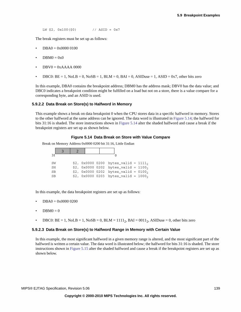
5.9 Breakpoint Examples
MIPS® EJTAG Specification, Revision 5.06 139
Copyright © 2000-2010 MIPS Technologies Inc. All rights reserved.
LW $2, 0x100($0) // ASID = 0x7
The break registers must be set up as follows:
• DBA0 = 0x0000 0100
• DBM0 = 0x0
• DBV0 = 0xAAAA 0000
• DBC0: BE = 1, NoLB = 0, NoSB = 1, BLM = 0, BAI = 0, ASIDuse = 1, ASID = 0x7, other bits zero
In this example, DBA0 contains the breakpoint address; DBM0 has the address mask; DBV0 has the data value; andDBC0 indicates a breakpoint condition might be fulfilled on a load but not on a store, there is a value compare for acorresponding byte, and an ASID is used.
5.9.2.2 Data Break on Store(s) to Halfword in Memory
This example shows a break on data breakpoint 0 when the CPU stores data in a specific halfword in memory. Storesto the other halfword at the same address can be ignored. The data word is illustrated in Figure 5.14; the halfword forbits 31:16 is shaded. The store instructions shown in Figure 5.14 alter the shaded halfword and cause a break if thebreakpoint registers are set up as shown below.
Figure 5.14 Data Break on Store with Value Compare
In this example, the data breakpoint registers are set up as follows:
• DBA0 = 0x0000 0200
• DBM0 = 0
• DBC0: BE = 1, NoLB = 1, NoSB = 0, BLM = 11112, BAI = 00112, ASIDuse = 0, other bits zero
5.9.2.3 Data Break on Store(s) to Halfword Range in Memory with Certain Value
In this example, the most significant halfword in a given memory range is altered, and the most significant part of thehalfword is written a certain value. The data word is illustrated below; the halfword for bits 31:16 is shaded. The storeinstructions shown in Figure 5.15 alter the shaded halfword and cause a break if the breakpoint registers are set up asshown below.
3 2
Break on Memory Address 0x0000 0200 bit 31:16, Little Endian
31 0
SW $2, 0x0000 0200 bytes_valid = 11112SH $2, 0x0000 0202 bytes_valid = 11002SB $2, 0x0000 0202 bytes_valid = 01002SB $2, 0x0000 0203 bytes_valid = 10002
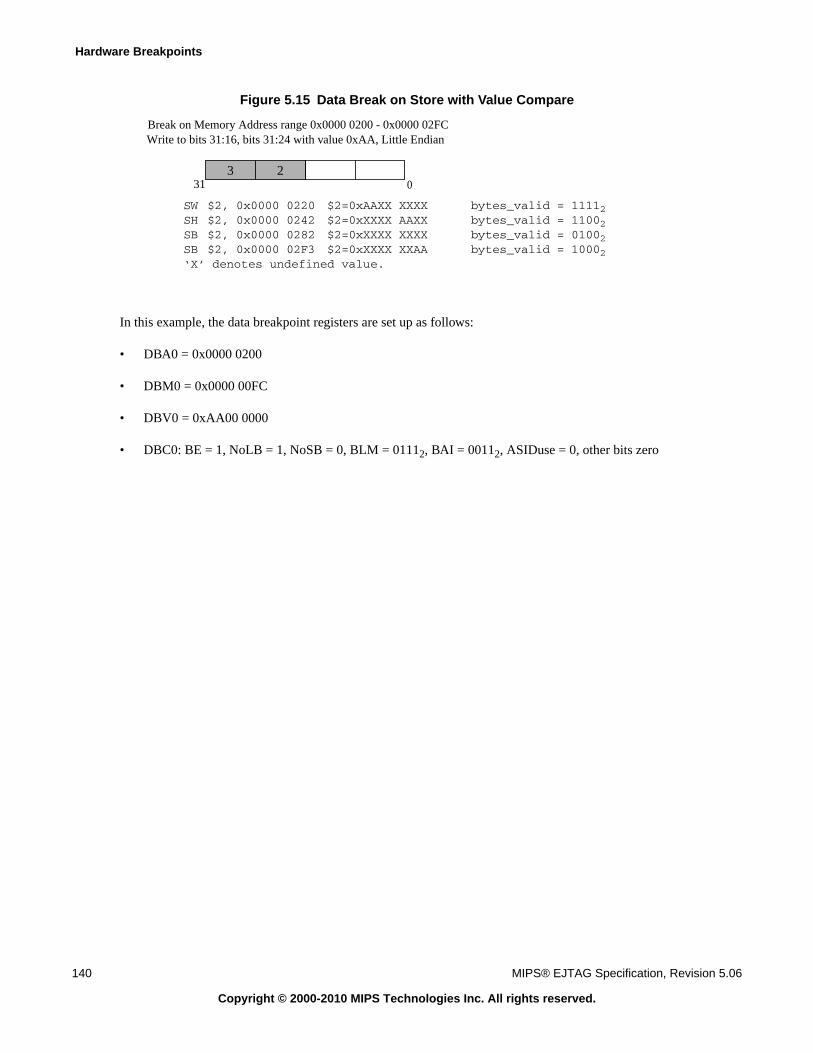
Hardware Breakpoints
140 MIPS® EJTAG Specification, Revision 5.06
Copyright © 2000-2010 MIPS Technologies Inc. All rights reserved.
Figure 5.15 Data Break on Store with Value Compare
In this example, the data breakpoint registers are set up as follows:
• DBA0 = 0x0000 0200
• DBM0 = 0x0000 00FC
• DBV0 = 0xAA00 0000
• DBC0: BE = 1, NoLB = 1, NoSB = 0, BLM = 01112, BAI = 00112, ASIDuse = 0, other bits zero
Break on Memory Address range 0x0000 0200 - 0x0000 02FC Write to bits 31:16, bits 31:24 with value 0xAA, Little Endian
SW $2, 0x0000 0220 $2=0xAAXX XXXX bytes_valid = 11112SH $2, 0x0000 0242 $2=0xXXXX AAXX bytes_valid = 11002SB $2, 0x0000 0282 $2=0xXXXX XXXX bytes_valid = 01002SB $2, 0x0000 02F3 $2=0xXXXX XXAA bytes_valid = 10002‘X’ denotes undefined value.
3 231 0
Chapter 6
MIPS® EJTAG Specification, Revision 5.06 141
Copyright © 2000-2010 MIPS Technologies Inc. All rights reserved.
Complex Break and Trigger Block
The complex break and trigger (CBT) block is part of the EJTAG breakpoint block and is therefore integrated into thecore logic when implemented. The CBT block is optional and defined in EJTAG spec 4.00 and above. A bit in theEJTAG DCRCBT register (bit 10) indicates the presence of this CBT block in the implementation. The CBT blockimplements complex breakpoint matching conditions that include: match primed by previous breakpoint match, qual-ified by previous data break match, matched using pass-counters, matches enabled by the and of two other breakmatches, etc.
The CBT block provides enhanced breakpoint and trace control capability based on the standard instruction and databreakpoints.
6.1 Complex Trigger Features/Capabilities
The complex trigger unit is typically integrated with the EJTAG simple break unit. All of the previous simple breakfeatures are preserved. This section describes the enhancements in the complex trigger block.
Note: the term breakpoints in this section refers to either actual breakpoints that take a debug exception or triggerpoints that only record the status and send this signal to the trace block.
• Pass Counters - each break channel has a counter associated with it that enables a breakpoint to only be takenafter the address/value condition has been met a certain number of times.
• Data Qualified breakpoints - these can be enabled and disabled based on the state of a data breakpoint conditionwhich can be used to only match on instructions executed in a certain process.
• Primed breakpoints - these are only enabled when another breakpoint has occurred which allows breaking on asimple sequences of events.
• Stopwatch timer - a counter that can be configured to start or stop based on specific instruction breakpoints.
• Ability to support ‘tuples’ - breakpoints that only fire when both instruction and data conditions match on a sin-gle instruction.
6.2 General Complex Break Behavior
There is some general complex break behavior that is common to all the features. This behavior is described below:
• Resets to a disabled state when the core is reset. The complex break functionality will be disabled and debugsoftware that is not aware of complex break should continue to function normally.
• Complex break state is not updated on exceptional instructions.
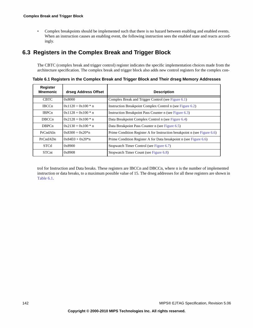
Complex Break and Trigger Block
142 MIPS® EJTAG Specification, Revision 5.06
Copyright © 2000-2010 MIPS Technologies Inc. All rights reserved.
• Complex breakpoints should be implemented such that there is no hazard between enabling and enabled events.When an instruction causes an enabling event, the following instruction sees the enabled state and reacts accord-ingly.
6.3 Registers in the Complex Break and Trigger Block
The CBTC (complex break and trigger control) register indicates the specific implementation choices made from thearchitecture specification. The complex break and trigger block also adds new control registers for the complex con-
trol for Instruction and Data breaks. These registers are IBCCn and DBCCn, where n is the number of implementedinstruction or data breaks, to a maximum possible value of 15. The drseg addresses for all these registers are shown inTable 6.1.
Table 6.1 Registers in the Complex Break and Trigger Block and Their drseg Memory Addresses
RegisterMnemonic drseg Address Offset Description
CBTC 0x8000 Complex Break and Trigger Control (see Figure 6.1)
IBCCn 0x1120 + 0x100 * n Instruction Breakpoint Complex Control n (see Figure 6.2)
IBPCn 0x1128 + 0x100 * n Instruction Breakpoint Pass Counter n (see Figure 6.3)
DBCCn 0x2128 + 0x100 * n Data Breakpoint Complex Control n (see Figure 6.4)
DBPCn 0x2130 + 0x100 * n Data Breakpoint Pass Counter n (see Figure 6.5)
PrCndAIn 0x8300 + 0x20*n Prime Condition Register A for Instruction breakpoint n (see Figure 6.6)
PrCndADn 0x84E0 + 0x20*n Prime Condition Register A for Data breakpoint n (see Figure 6.6)
STCtl 0x8900 Stopwatch Timer Control (see Figure 6.7)
STCnt 0x8908 Stopwatch Timer Count (see Figure 6.8)
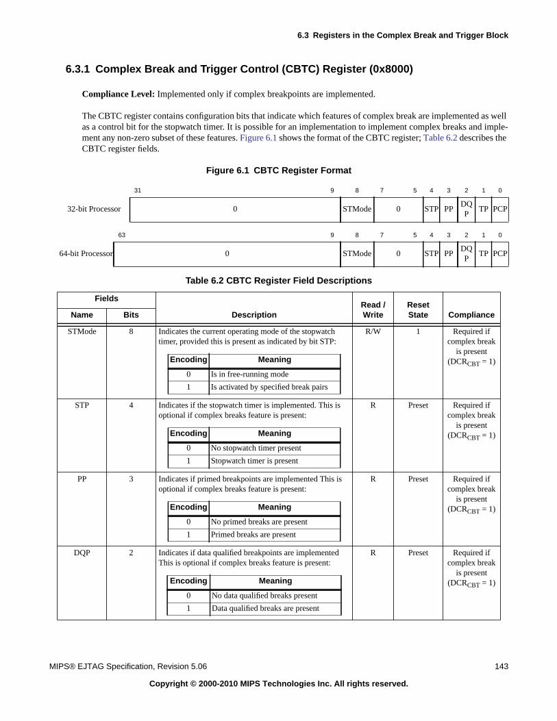
6.3 Registers in the Complex Break and Trigger Block
MIPS® EJTAG Specification, Revision 5.06 143
Copyright © 2000-2010 MIPS Technologies Inc. All rights reserved.
6.3.1 Complex Break and Trigger Control (CBTC) Register (0x8000)
Compliance Level: Implemented only if complex breakpoints are implemented.
The CBTC register contains configuration bits that indicate which features of complex break are implemented as wellas a control bit for the stopwatch timer. It is possible for an implementation to implement complex breaks and imple-ment any non-zero subset of these features. Figure 6.1 shows the format of the CBTC register; Table 6.2 describes theCBTC register fields.
Figure 6.1 CBTC Register Format
31 9 8 7 5 4 3 2 1 0
32-bit Processor 0 STMode 0 STP PPDQP
TP PCP
63 9 8 7 5 4 3 2 1 0
64-bit Processor 0 STMode 0 STP PPDQP
TP PCP
Table 6.2 CBTC Register Field Descriptions
Fields
DescriptionRead /Write
ResetState ComplianceName Bits
STMode 8 Indicates the current operating mode of the stopwatchtimer, provided this is present as indicated by bit STP:
R/W 1 Required ifcomplex break
is present(DCRCBT = 1)
STP 4 Indicates if the stopwatch timer is implemented. This isoptional if complex breaks feature is present:
R Preset Required ifcomplex break
is present(DCRCBT = 1)
PP 3 Indicates if primed breakpoints are implemented This isoptional if complex breaks feature is present:
R Preset Required ifcomplex break
is present(DCRCBT = 1)
DQP 2 Indicates if data qualified breakpoints are implementedThis is optional if complex breaks feature is present:
R Preset Required ifcomplex break
is present(DCRCBT = 1)
Encoding Meaning
0 Is in free-running mode
1 Is activated by specified break pairs
Encoding Meaning
0 No stopwatch timer present
1 Stopwatch timer is present
Encoding Meaning
0 No primed breaks are present
1 Primed breaks are present
Encoding Meaning
0 No data qualified breaks present
1 Data qualified breaks are present
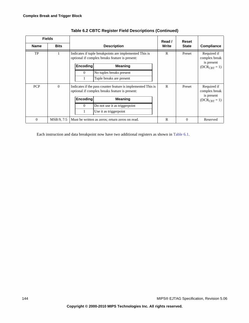
Complex Break and Trigger Block
144 MIPS® EJTAG Specification, Revision 5.06
Copyright © 2000-2010 MIPS Technologies Inc. All rights reserved.
Each instruction and data breakpoint now have two additional registers as shown in Table 6.1.
TP 1 Indicates if tuple breakpoints are implemented This isoptional if complex breaks feature is present:
R Preset Required ifcomplex break
is present(DCRCBT = 1)
PCP 0 Indicates if the pass counter feature is implemented This isoptional if complex breaks feature is present:
R Preset Required ifcomplex break
is present(DCRCBT = 1)
0 MSB:9, 7:5 Must be written as zeros; return zeros on read. R 0 Reserved
Table 6.2 CBTC Register Field Descriptions (Continued)
Fields
DescriptionRead /Write
ResetState ComplianceName Bits
Encoding Meaning
0 No tuples breaks present
1 Tuple breaks are present
Encoding Meaning
0 Do not use it as triggerpoint
1 Use it as triggerpoint
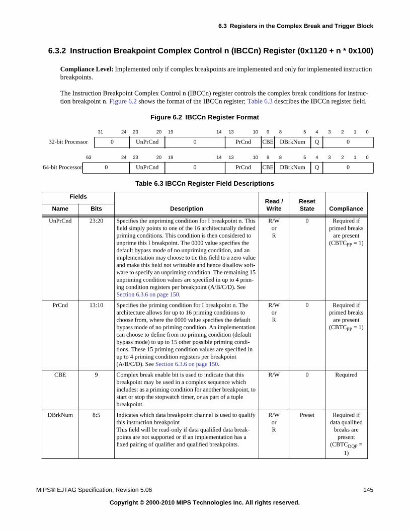
6.3 Registers in the Complex Break and Trigger Block
MIPS® EJTAG Specification, Revision 5.06 145
Copyright © 2000-2010 MIPS Technologies Inc. All rights reserved.
6.3.2 Instruction Breakpoint Complex Control n (IBCCn) Register (0x1120 + n * 0x100)
Compliance Level: Implemented only if complex breakpoints are implemented and only for implemented instructionbreakpoints.
The Instruction Breakpoint Complex Control n (IBCCn) register controls the complex break conditions for instruc-tion breakpoint n. Figure 6.2 shows the format of the IBCCn register; Table 6.3 describes the IBCCn register field.
Figure 6.2 IBCCn Register Format
31 24 23 20 19 14 13 10 9 8 5 4 3 2 1 0
32-bit Processor 0 UnPrCnd 0 PrCnd CBE DBrkNum Q 0
63 24 23 20 19 14 13 10 9 8 5 4 3 2 1 0
64-bit Processor 0 UnPrCnd 0 PrCnd CBE DBrkNum Q 0
Table 6.3 IBCCn Register Field Descriptions
Fields
DescriptionRead /Write
ResetState ComplianceName Bits
UnPrCnd 23:20 Specifies the unpriming condition for I breakpoint n. Thisfield simply points to one of the 16 architecturally definedpriming conditions. This condition is then considered tounprime this I breakpoint. The 0000 value specifies thedefault bypass mode of no unpriming condition, and animplementation may choose to tie this field to a zero valueand make this field not writeable and hence disallow soft-ware to specify an unpriming condition. The remaining 15unpriming condition values are specified in up to 4 prim-ing condition registers per breakpoint (A/B/C/D). SeeSection 6.3.6 on page 150.
R/WorR
0 Required ifprimed breaks
are present(CBTCPP = 1)
PrCnd 13:10 Specifies the priming condition for I breakpoint n. Thearchitecture allows for up to 16 priming conditions tochoose from, where the 0000 value specifies the defaultbypass mode of no priming condition. An implementationcan choose to define from no priming condition (defaultbypass mode) to up to 15 other possible priming condi-tions. These 15 priming condition values are specified inup to 4 priming condition registers per breakpoint(A/B/C/D). See Section 6.3.6 on page 150.
R/WorR
0 Required ifprimed breaks
are present(CBTCPP = 1)
CBE 9 Complex break enable bit is used to indicate that thisbreakpoint may be used in a complex sequence whichincludes: as a priming condition for another breakpoint, tostart or stop the stopwatch timer, or as part of a tuplebreakpoint.
R/W 0 Required
DBrkNum 8:5 Indicates which data breakpoint channel is used to qualifythis instruction breakpointThis field will be read-only if data qualified data break-points are not supported or if an implementation has afixed pairing of qualifier and qualified breakpoints.
R/WorR
Preset Required ifdata qualified
breaks arepresent
(CBTCDQP =
1)
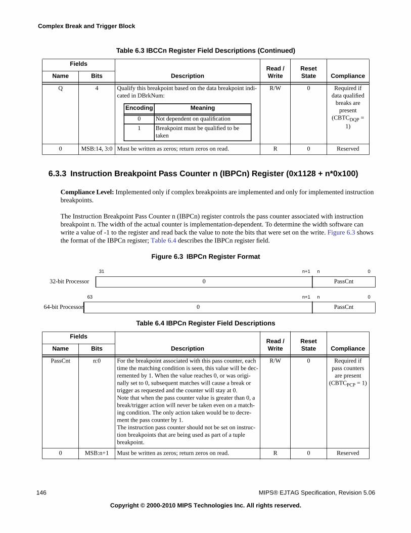
Complex Break and Trigger Block
146 MIPS® EJTAG Specification, Revision 5.06
Copyright © 2000-2010 MIPS Technologies Inc. All rights reserved.
6.3.3 Instruction Breakpoint Pass Counter n (IBPCn) Register (0x1128 + n*0x100)
Compliance Level: Implemented only if complex breakpoints are implemented and only for implemented instructionbreakpoints.
The Instruction Breakpoint Pass Counter n (IBPCn) register controls the pass counter associated with instructionbreakpoint n. The width of the actual counter is implementation-dependent. To determine the width software canwrite a value of -1 to the register and read back the value to note the bits that were set on the write. Figure 6.3 showsthe format of the IBPCn register; Table 6.4 describes the IBPCn register field.
Figure 6.3 IBPCn Register Format
Q 4 Qualify this breakpoint based on the data breakpoint indi-cated in DBrkNum:
R/W 0 Required ifdata qualified
breaks arepresent
(CBTCDQP =
1)
0 MSB:14, 3:0 Must be written as zeros; return zeros on read. R 0 Reserved
31 n+1 n 0
32-bit Processor 0 PassCnt
63 n+1 n 0
64-bit Processor 0 PassCnt
Table 6.4 IBPCn Register Field Descriptions
Fields
DescriptionRead /Write
ResetState ComplianceName Bits
PassCnt n:0 For the breakpoint associated with this pass counter, eachtime the matching condition is seen, this value will be dec-remented by 1. When the value reaches 0, or was origi-nally set to 0, subsequent matches will cause a break ortrigger as requested and the counter will stay at 0.Note that when the pass counter value is greater than 0, abreak/trigger action will never be taken even on a match-ing condition. The only action taken would be to decre-ment the pass counter by 1.The instruction pass counter should not be set on instruc-tion breakpoints that are being used as part of a tuplebreakpoint.
R/W 0 Required ifpass counters
are present(CBTCPCP = 1)
0 MSB:n+1 Must be written as zeros; return zeros on read. R 0 Reserved
Table 6.3 IBCCn Register Field Descriptions (Continued)
Fields
DescriptionRead /Write
ResetState ComplianceName Bits
Encoding Meaning
0 Not dependent on qualification
1 Breakpoint must be qualified to betaken
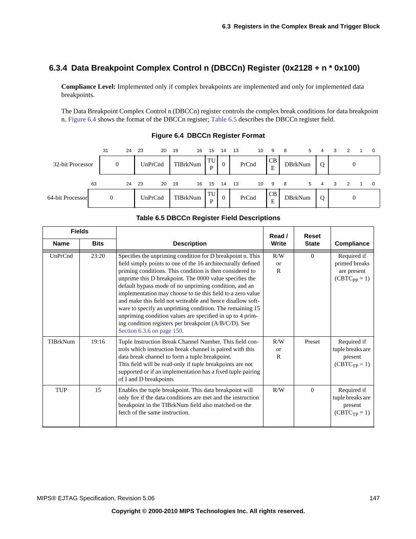
6.3 Registers in the Complex Break and Trigger Block
MIPS® EJTAG Specification, Revision 5.06 147
Copyright © 2000-2010 MIPS Technologies Inc. All rights reserved.
6.3.4 Data Breakpoint Complex Control n (DBCCn) Register (0x2128 + n * 0x100)
Compliance Level: Implemented only if complex breakpoints are implemented and only for implemented databreakpoints.
The Data Breakpoint Complex Control n (DBCCn) register controls the complex break conditions for data breakpointn. Figure 6.4 shows the format of the DBCCn register; Table 6.5 describes the DBCCn register field.
Figure 6.4 DBCCn Register Format
31 24 23 20 19 16 15 14 13 10 9 8 5 4 3 2 1 0
32-bit Processor 0 UnPrCnd TIBrkNumTUP
0 PrCndCBE
DBrkNum Q 0
63 24 23 20 19 16 15 14 13 10 9 8 5 4 3 2 1 0
64-bit Processor 0 UnPrCnd TIBrkNumTUP
0 PrCndCBE
DBrkNum Q 0
Table 6.5 DBCCn Register Field Descriptions
Fields
DescriptionRead /Write
ResetState ComplianceName Bits
UnPrCnd 23:20 Specifies the unpriming condition for D breakpoint n. Thisfield simply points to one of the 16 architecturally definedpriming conditions. This condition is then considered tounprime this D breakpoint. The 0000 value specifies thedefault bypass mode of no unpriming condition, and animplementation may choose to tie this field to a zero valueand make this field not writeable and hence disallow soft-ware to specify an unpriming condition. The remaining 15unpriming condition values are specified in up to 4 prim-ing condition registers per breakpoint (A/B/C/D). SeeSection 6.3.6 on page 150.
R/WorR
0 Required ifprimed breaks
are present(CBTCPP = 1)
TIBrkNum 19:16 Tuple Instruction Break Channel Number. This field con-trols which instruction break channel is paired with thisdata break channel to form a tuple breakpoint.This field will be read-only if tuple breakpoints are notsupported or if an implementation has a fixed tuple pairingof I and D breakpoints
R/WorR
Preset Required iftuple breaks are
present(CBTCTP = 1)
TUP 15 Enables the tuple breakpoint. This data breakpoint willonly fire if the data conditions are met and the instructionbreakpoint in the TIBrkNum field also matched on thefetch of the same instruction.
R/W 0 Required iftuple breaks are
present(CBTCTP = 1)
Complex Break and Trigger Block
148 MIPS® EJTAG Specification, Revision 5.06
Copyright © 2000-2010 MIPS Technologies Inc. All rights reserved.
PrCnd 13:10 Specifies the priming condition for D breakpoint n. Thearchitecture allows for up to 16 priming conditions tochoose from, where the 0000 value specifies the defaultbypass mode of no priming condition. An implementationcan choose to define from no priming condition (defaultbypass mode) to up to 15 other possible priming condi-tion. These 15 priming condition values are specified in upto 4 priming condition registers per breakpoint (A/B/C/D).See Section 6.3.6 on page 150.
R/W 0 Required ifprimed breaks
are present(CBTCPP = 1)
CBE 9 Complex break enable bit is used to indicate that thisbreakpoint may be used in a complex sequence whichincludes: as a priming or qualifying condition for anotherbreakpoint, or to start or stop the stopwatch timer.
R/W 0 Required
DBrkNum 8:5 Indicates which data breakpoint channel is used to qualifythis data breakpoint.This field will be read-only if data qualified data break-points are not supported or if an implementation has afixed pairing of qualifier and qualified breakpoints.
R/WorR
Preset Required ifdata qualified
breaks arepresent
(CBTCDQP =
1)
Q 4 Qualify this breakpoint based on the data breakpoint indi-cated in DBrkNum:
R/W 0 Required ifdata qualified
breaks arepresent
(CBTCDQP =
1)
0 MSB:24, 14,3:0
Must be written as zeros; return zeros on read. R 0 Reserved
Table 6.5 DBCCn Register Field Descriptions (Continued)
Fields
DescriptionRead /Write
ResetState ComplianceName Bits
Encoding Meaning
0 Not dependent on qualification
1 Breakpoint must be qualified to betaken
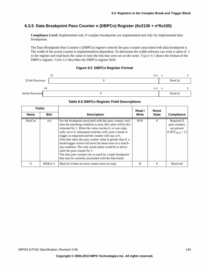
6.3 Registers in the Complex Break and Trigger Block
MIPS® EJTAG Specification, Revision 5.06 149
Copyright © 2000-2010 MIPS Technologies Inc. All rights reserved.
6.3.5 Data Breakpoint Pass Counter n (DBPCn) Register (0x2130 + n*0x100)
Compliance Level: Implemented only if complex breakpoints are implemented and only for implemented databreakpoints.
The Data Breakpoint Pass Counter n (DBPCn) register controls the pass counter associated with data breakpoint n.The width of the actual counter is implementation-dependent. To determine the width software can write a value of -1to the register and read back the value to note the bits that were set on the write. Figure 6.5 shows the format of theDBPCn register; Table 6.6 describes the DBPCn register field.
Figure 6.5 DBPCn Register Format
31 n+1 n 0
32-bit Processor 0 PassCnt
63 n+1 n 0
64-bit Processor 0 PassCnt
Table 6.6 DBPCn Register Field Descriptions
Fields
DescriptionRead /Write
ResetState ComplianceName Bits
PassCnt n:0 For the breakpoint associated with this pass counter, eachtime the matching condition is seen, this value will be dec-remented by 1. When the value reaches 0, or was origi-nally set to 0, subsequent matches will cause a break ortrigger as requested and the counter will stay at 0.Note that when the pass counter value is greater than 0, abreak/trigger action will never be taken even on a match-ing condition. The only action taken would be to decre-ment the pass counter by 1.The data pass counters are re-used for a tuple breakpointthat may be currently associated with the data break.
R/W 0 Required ifpass counters
are present(CBTCPCP = 1)
0 MSB:n+1 Must be written as zeros; return zeros on read. R 0 Reserved
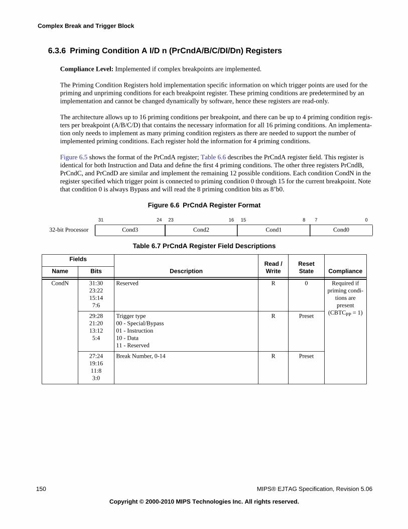
Complex Break and Trigger Block
150 MIPS® EJTAG Specification, Revision 5.06
Copyright © 2000-2010 MIPS Technologies Inc. All rights reserved.
6.3.6 Priming Condition A I/D n (PrCndA/B/C/DI/Dn) Registers
Compliance Level: Implemented if complex breakpoints are implemented.
The Priming Condition Registers hold implementation specific information on which trigger points are used for thepriming and unpriming conditions for each breakpoint register. These priming conditions are predetermined by animplementation and cannot be changed dynamically by software, hence these registers are read-only.
The architecture allows up to 16 priming conditions per breakpoint, and there can be up to 4 priming condition regis-ters per breakpoint (A/B/C/D) that contains the necessary information for all 16 priming conditions. An implementa-tion only needs to implement as many priming condition registers as there are needed to support the number ofimplemented priming conditions. Each register hold the information for 4 priming conditions.
Figure 6.5 shows the format of the PrCndA register; Table 6.6 describes the PrCndA register field. This register isidentical for both Instruction and Data and define the first 4 priming conditions. The other three registers PrCndB,PrCndC, and PrCndD are similar and implement the remaining 12 possible conditions. Each condition CondN in theregister specified which trigger point is connected to priming condition 0 through 15 for the current breakpoint. Notethat condition 0 is always Bypass and will read the 8 priming condition bits as 8’b0.
Figure 6.6 PrCndA Register Format
31 24 23 16 15 8 7 0
32-bit Processor Cond3 Cond2 Cond1 Cond0
Table 6.7 PrCndA Register Field Descriptions
Fields
DescriptionRead /Write
ResetState ComplianceName Bits
CondN 31:3023:2215:147:6
Reserved R 0 Required ifpriming condi-
tions arepresent
(CBTCPP = 1)29:2821:2013:125:4
Trigger type00 - Special/Bypass01 - Instruction10 - Data11 - Reserved
R Preset
27:2419:1611:83:0
Break Number, 0-14 R Preset
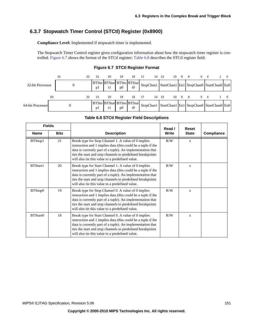
6.3 Registers in the Complex Break and Trigger Block
MIPS® EJTAG Specification, Revision 5.06 151
Copyright © 2000-2010 MIPS Technologies Inc. All rights reserved.
6.3.7 Stopwatch Timer Control (STCtl) Register (0x8900)
Compliance Level: Implemented if stopwatch timer is implemented.
The Stopwatch Timer Control register gives configuration information about how the stopwatch timer register is con-trolled. Figure 6.7 shows the format of the STCtl register; Table 6.8 describes the STCtl register field.
Figure 6.7 STCtl Register Format
31 22 21 20 19 18 17 14 13 10 9 8 5 4 1 0
32-bit Processor 0BTSto
p1BTStar
t1BTSto
p0BTStar
t0StopChan1 StartChan1 En1 StopChan0 StartChan0 En0
63 22 21 20 19 18 17 14 13 10 9 8 5 4 1 0
64-bit Processor 0BTSto
p1BTStar
t1BTSto
p0BTStar
t0StopChan1 StartChan1 En1 StopChan0 StartChan0 En0
Table 6.8 STCtl Register Field Descriptions
Fields
DescriptionRead /Write
ResetState ComplianceName Bits
BTStop1 21 Break type for Stop Channel 1. A value of 0 impliesinstruction and 1 implies data (this could be a tuple if thedata is currently part of a tuple). An implementation thatties the start and stop channels to predefined breakpointswill also tie this value to a predefined value.
R/W x
BTStart1 20 Break type for Start Channel 1. A value of 0 impliesinstruction and 1 implies data (this could be a tuple if thedata is currently part of a tuple). An implementation thatties the start and stop channels to predefined breakpointswill also tie this value to a predefined value.
R/W x
BTStop0 19 Break type for Stop Channel 0. A value of 0 impliesinstruction and 1 implies data (this could be a tuple if thedata is currently part of a tuple). An implementation thatties the start and stop channels to predefined breakpointswill also tie this value to a predefined value.
R/W x
BTStart0 18 Break type for Start Channel 0. A value of 0 impliesinstruction and 1 implies data (this could be a tuple if thedata is currently part of a tuple). An implementation thatties the start and stop channels to predefined breakpointswill also tie this value to a predefined value.
R/W x
Complex Break and Trigger Block
152 MIPS® EJTAG Specification, Revision 5.06
Copyright © 2000-2010 MIPS Technologies Inc. All rights reserved.
StopChan1 17:14 Indicates the breakpoint channel for the second pair thatwill stop the counter if the timer is under breakpoint con-trol. An implementation can choose to tie this to a pre-defined breakpoint. But it is possible for implementationto allow this field to be writable by software so that thepair of start and start channels is dynamically selectable.
R/W x Optional
StartChan1 13:10 Indicates the breakpoint channel for the second pair thatwill start the counter if the timer is under breakpoint con-trol. An implementation can choose to tie this to a pre-defined breakpoint. But it is possible for implementationto allow this field to be writable by software so that thepair of start and start channels is dynamically selectable.
R/W x
En1 9 Enable the second pair of breakpoint registers to controlthe timer under breakpoint control.
R/W x
StopChan0 8:5 Indicates the breakpoint channel that will stop the counterif the timer is under breakpoint control. An implementa-tion can choose to tie this to a predefined breakpoint. Butit is possible for implementation to allow this field to bewritable by software so that the pair of start and start chan-nels is dynamically selectable.
R/W x Required ifstopwatch
timer is present(CBTCSTP = 1)
StartChan0 4:1 Indicates the breakpoint channel that will start the counterif the timer is under breakpoint control. An implementa-tion can choose to tie this to a predefined breakpoint. Butit is possible for implementation to allow this field to bewritable by software so that the pair of start and start chan-nels is dynamically selectable.
R/W x
En0 0 Enable the first pair of breakpoint registers to control thetimer under breakpoint control.
R/W x
0 MSB:22 Must be written as zero; returns zero on read. R 0 Reserved
Table 6.8 STCtl Register Field Descriptions (Continued)
Fields
DescriptionRead /Write
ResetState ComplianceName Bits
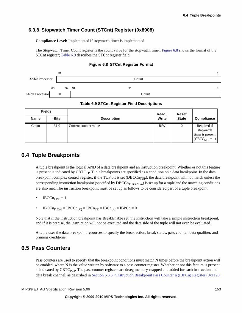
6.4 Tuple Breakpoints
MIPS® EJTAG Specification, Revision 5.06 153
Copyright © 2000-2010 MIPS Technologies Inc. All rights reserved.
6.3.8 Stopwatch Timer Count (STCnt) Register (0x8908)
Compliance Level: Implemented if stopwatch timer is implemented.
The Stopwatch Timer Count register is the count value for the stopwatch timer. Figure 6.8 shows the format of theSTCnt register; Table 6.9 describes the STCnt register field.
Figure 6.8 STCnt Register Format
6.4 Tuple Breakpoints
A tuple breakpoint is the logical AND of a data breakpoint and an instruction breakpoint. Whether or not this featureis present is indicated by CBTCTP. Tuple breakpoints are specified as a condition on a data breakpoint. In the databreakpoint complex control register, if the TUP bit is set (DBCCnTUP), the data breakpoint will not match unless thecorresponding instruction breakpoint (specified by DBCCnTIBrkNum) is set up for a tuple and the matching conditionsare also met. The instruction breakpoint must be set up as follows to be considered part of a tuple breakpoint:
• IBCCnCBE = 1
• IBCCnPrCnd = IBCCnDQ = IBCnTE = IBCnBE = IBPCn = 0
Note that if the instruction breakpoint has BreakEnable set, the instruction will take a simple instruction breakpoint,and if it is precise, the instruction will not be executed and the data side of the tuple will not even be evaluated.
A tuple uses the data breakpoint resources to specify the break action, break status, pass counter, data qualifier, andpriming conditions.
6.5 Pass Counters
Pass counters are used to specify that the breakpoint conditions must match N times before the breakpoint action willbe enabled, where N is the value written by software to a pass counter register. Whether or not this feature is presentis indicated by CBTCPCP. The pass counter registers are drseg memory-mapped and added for each instruction anddata break channel, as described in Section 6.3.3 “Instruction Breakpoint Pass Counter n (IBPCn) Register (0x1128
31 0
32-bit Processor Count
63 32 31 31 0
64-bit Processor 0 Count
Table 6.9 STCnt Register Field Descriptions
Fields
DescriptionRead /Write
ResetState ComplianceName Bits
Count 31:0 Current counter value R/W 0 Required ifstopwatch
timer is present(CBTCSTP = 1)
Complex Break and Trigger Block
154 MIPS® EJTAG Specification, Revision 5.06
Copyright © 2000-2010 MIPS Technologies Inc. All rights reserved.
+ n*0x100)” and Section 6.3.5 “Data Breakpoint Pass Counter n (DBPCn) Register (0x2130 + n*0x100)”. The databreakpoint pass counter registers are reused for tuple breakpoints. Pass counter usage is specified below.
• The architecture allows an implementation to implement pass counters on a subset of the implemented instruc-tion and data breakpoints.
• The width of the counter is also implementation-dependent. Software can determine the width and presence of acounter by writing a value of -1 to the register and reading back to see which bits are set. When no bits are set,this implies that this breakpoint does not implement a pass counter. The recommended counter size is 8 bits forinstruction breakpoints and 16 bits for data breakpoints.
• Writing a non-zero value to this register will enable the pass counters. When enabled, each time the breakpointconditions match, the counter will be decremented by 1. When the counter value reaches 0, the breakpoint action(breakpoint exception, trigger, or complex break enable) will occur on any subsequent matches, and the counterwill not decrement further.
• If the breakpoint also has priming conditions and/or data qualifier specified, the pass counter will only decrementwhen the priming and/or data qualifier conditions have been met. A breakpoint condition can be changed frombeing qualified to unqualified or primed to unprimed without any affect on the counter state.
• If a data breakpoint is configured to be a tuple breakpoint, the data pass counter will only decrement on instruc-tions where both the instruction and data break conditions match. The pass counter for the instruction breakinvolved in a tuple should not be enabled if the tuple is enabled.
• Writing a value of 0 to the counter will disable the pass counter and enable the breakpoint to fire whenever theconditions are met. The counter is reset to 0 to preserve compatibility with legacy software.
• The counter register will be updated as matches are detected, and the current value can be read from the registerwhile operating in debug mode. It is not a requirement, but an architectural recommendation that the currentcount value be reflected in the drseg register that represents the counter.
• In some implementations, a simple instruction breakpoint may be taken precisely, while a complex breakpoint,like the one that uses pass counters, may be taken imprecisely. In this situation, when a complex condition likepass counters is disabled during execution, the breakpoint exceptions will continue to be taken imprecisely untilthe complex condition is cleared, for example, when the pass counter is actually written with the zero value.
6.6 Data Qualified Breakpoints
Each of the breakpoints, instruction, data, or tuple can be data qualified. Whether or not this feature is present is indi-cated by CBTCDQ. In qualified mode, a breakpoint will recognize its conditions only after the specified data break-point matches both address and data. If the qualifying data breakpoint matches the address but has a mismatch on thedata value, the breakpoint with the qualifier will be disqualified and will not match until a subsequent qualifyingmatch.
The pairing of which data break qualifies a breakpoint is specified in IBCCnDBrkNum and DBCCnDBrkNum. Thesefields will be read-only if an implemtation has a fixed pairing of qualifying and qualified breakpoints and will be writ-able if dynamic pairing is supported. The IBCCnQ and DBCCQ bits are used by software to decide when an instruc-tion or data breakpoint respectively should be actively considered to be data qualified. See Section 6.3.2 “InstructionBreakpoint Complex Control n (IBCCn) Register (0x1120 + n * 0x100)” and Section 6.3.4 “Data BreakpointComplex Control n (DBCCn) Register (0x2128 + n * 0x100)”. The tuple breakpoint reuses the bits in the correspond-ing DBCCn register of the data breakpoint that forms the tuple.
6.7 Primed Breakpoints
MIPS® EJTAG Specification, Revision 5.06 155
Copyright © 2000-2010 MIPS Technologies Inc. All rights reserved.
This feature can be used similarly to the ASID qualification that is available on cores with TLBs. If an RTOS loads aprocess ID for the current process, that load can be used as the qualifying breakpoint. When a matching process ID isloaded (entering the desired RTOS process), qualified instruction breakpoints will be enabled. When a different pro-cess IS is loaded (leaving the desired RTOS process), the qualified instruction breakpoints are disabled. Alternatively,with the InvertValueMatch feature of the data breakpoint, the instruction breakpoints could be enabled on a any pro-cess ID other than the specified one.
Enabling the data qualifier requires the following to be true:
• Qualifier (data break) must have DBCnTE or DBCCnCBE set.
• Qualifier should have data comparison enabled (via settings of DBCnBLM and DBCnBAI).
• Qualifier should not have pass counters, priming conditions, data qualification, or tuples enabled.
• Qualifier can be either a load or store instruction (as enabled by DBCnNoLB/NoSB)
6.7 Primed Breakpoints
Priming conditions provide a way for one breakpoint to be enabled or disabled by another one. Whether or not thisfeature is present is indicated by CBTCPP. Prior to the priming condition being satisfied, any breakpoint matches areignored. It is possible for a primed breakpoint to get unprimed. Once unprimed, the breakpoint must be primed againbefore a matching condition will enable the breakpoint to take a break or trigger action. The details of this feature are:
• Each breakpoint has a choice of up to a maximum of 16 possible priming conditions. An implementation maylimit this to a smaller number and will list the specific priming conditions for each of its breakpoints for refer-ence. The priming conditions vary from breakpoint to breakpoint (since it makes no sense for a breakpoint toprime itself).
• Each Prime condition is the comparator output after it has been qualified by its own Prime condition and passcounter. Using this, several stages of Priming are possible (e.g. data cycle D followed by instruction A followedby instruction B followed by instruction C).
• One of the conditions is a bypass mode in which the priming condition is always met. This bypass condition isthe default state of a breakpoint and initialized on reset to be backwards compatible to the simple instruction anddata breakpoints.
• The priming breakpoint must have IBCnTE or IBCCnCBE set if it is an instruction breakpoint, or it must haveDBCnTE or DBCCnCBE set if it is a data (or tuple) breakpoint.
• The IBCCnUnPrCnd and DBCCnUnPrCnd are used to specify a condition used to unprime the instruction or databreakpoint respectively. This is optional since an implementation can tie this field to 0 and disallowing softwareto write to this field. This implies that the unprime feature is a bypass and it is not possible to unprime a break-point once it is primed. A breakpoint is considered to start in the unprimed condition until it matches a primingcondition. Encountering an unprime condition match will take the breakpoint to the unprime state if it wasprimed, or leave it unprimed if it was already in the unprimed state.
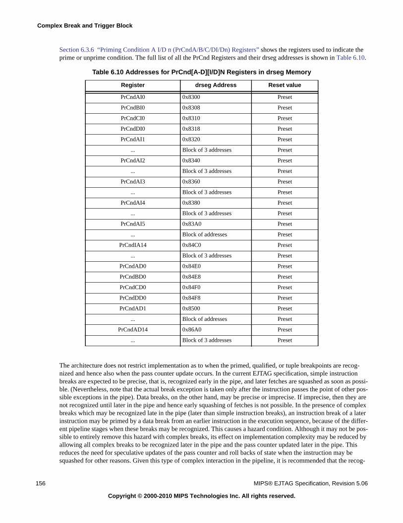
Complex Break and Trigger Block
156 MIPS® EJTAG Specification, Revision 5.06
Copyright © 2000-2010 MIPS Technologies Inc. All rights reserved.
Section 6.3.6 “Priming Condition A I/D n (PrCndA/B/C/DI/Dn) Registers” shows the registers used to indicate theprime or unprime condition. The full list of all the PrCnd Registers and their drseg addresses is shown in Table 6.10.
The architecture does not restrict implementation as to when the primed, qualified, or tuple breakpoints are recog-nized and hence also when the pass counter update occurs. In the current EJTAG specification, simple instructionbreaks are expected to be precise, that is, recognized early in the pipe, and later fetches are squashed as soon as possi-ble. (Nevertheless, note that the actual break exception is taken only after the instruction passes the point of other pos-sible exceptions in the pipe). Data breaks, on the other hand, may be precise or imprecise. If imprecise, then they arenot recognized until later in the pipe and hence early squashing of fetches is not possible. In the presence of complexbreaks which may be recognized late in the pipe (later than simple instruction breaks), an instruction break of a laterinstruction may be primed by a data break from an earlier instruction in the execution sequence, because of the differ-ent pipeline stages when these breaks may be recognized. This causes a hazard condition. Although it may not be pos-sible to entirely remove this hazard with complex breaks, its effect on implementation complexity may be reduced byallowing all complex breaks to be recognized later in the pipe and the pass counter updated later in the pipe. Thisreduces the need for speculative updates of the pass counter and roll backs of state when the instruction may besquashed for other reasons. Given this type of complex interaction in the pipeline, it is recommended that the recog-
Table 6.10 Addresses for PrCnd[A-D][I/D]N Registers in drseg Memory
Register drseg Address Reset value
PrCndAI0 0x8300 Preset
PrCndBI0 0x8308 Preset
PrCndCI0 0x8310 Preset
PrCndDI0 0x8318 Preset
PrCndAI1 0x8320 Preset
... Block of 3 addresses Preset
PrCndAI2 0x8340 Preset
... Block of 3 addresses Preset
PrCndAI3 0x8360 Preset
... Block of 3 addresses Preset
PrCndAI4 0x8380 Preset
... Block of 3 addresses Preset
PrCndAI5 0x83A0 Preset
... Block of addresses Preset
PrCndIA14 0x84C0 Preset
... Block of 3 addresses Preset
PrCndAD0 0x84E0 Preset
PrCndBD0 0x84E8 Preset
PrCndCD0 0x84F0 Preset
PrCndDD0 0x84F8 Preset
PrCndAD1 0x8500 Preset
... Block of addresses Preset
PrCndAD14 0x86A0 Preset
... Block of 3 addresses Preset
6.8 Stopwatch Timer
MIPS® EJTAG Specification, Revision 5.06 157
Copyright © 2000-2010 MIPS Technologies Inc. All rights reserved.
nition of simple instruction breaks be retained at the early pipe stages, while all complex break recognition be delayedto the stage where the data breaks are recognized.
6.8 Stopwatch Timer
The stopwatch timer is a count register that is memory-mapped to drseg so that it can be read and reset by software(see Section 6.3.8 “Stopwatch Timer Count (STCnt) Register (0x8908)”). The presence of this feature is indicated bybit CBTCSTP. A stopwatch control register is used to control its operation (see Section 6.3.7 “Stopwatch TimerControl (STCtl) Register (0x8900)”). The stopwatch timer works as follows:
• Count value is reset to 0.
• The timer can be configured to be in a free running mode or controlled to start and stop by specific breakpointsusing CBTCSTMode.
• The ability to start and stop the timer using breakpoints can be a useful feature. For example, by using instructionbreaks to start and stop the timer, it would be possible to measure the amount of time spent in a particular body ofcode by setting the start break channel to point to the entry point and the stop break channel to point to the exitpoint.
• The architecture allows up to two pairs of start/stop break channels. An implementation can choose to implementonly one pair. If the stopwatch timer feature is implemented, then at least one pair of start/stop breakpoints mustbe implemented.
• Reset state has counter stopped and under breakpoint control, so that the counter is not running when the core isnot being actively debugged.
• The counter stops counting on entry into debug mode.
• When controlled by breakpoints, the controlling breakpoints should have the corresponding IBCnTE or IBC-CnCBE bit set for instructions breaks and the bit set for data (or tuple) breaks.
• The architecture allows software to program the start and stop hardware breakpoints, but an implementation canchoose to predetermine these breakpoints, only allowing software the ability to enable one pair or the other. Soft-ware must write -1 to the STCtl register and read back the value to determine whether or not an implementationhas provided software with the ability to program the start/stop breaks and how many pairs are implemented.
• Note that if two pairs are implemented, then enabling both will cause the hardware to use pair 0 as the controllingpair.
6.9 Reporting of the Complex Breakpoints in the Debug Register
Described here are the changes to the Debug register (number 23, select 0) and a new CP0 register Debug2 (number23, select 6) which are used to report the cause of debug breaks when the cause arises from a complex breakpoint.
6.9.1 Debug Register (23, select 0) Changes for Complex Breakpoints
The Debug register now defines the DIBImpr field, which indicates if a Debug Instruction Break exception occurredon an instruction due to an imprecise instruction hardware break.
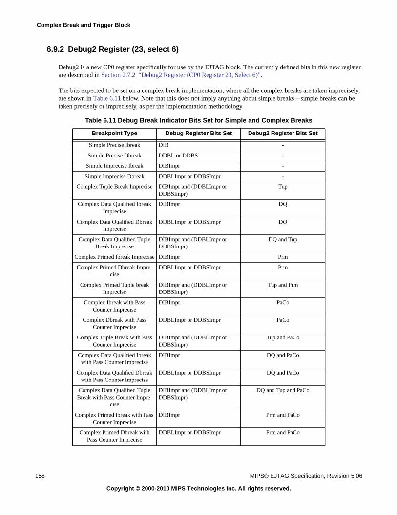
Complex Break and Trigger Block
158 MIPS® EJTAG Specification, Revision 5.06
Copyright © 2000-2010 MIPS Technologies Inc. All rights reserved.
6.9.2 Debug2 Register (23, select 6)
Debug2 is a new CP0 register specifically for use by the EJTAG block. The currently defined bits in this new registerare described in Section 2.7.2 “Debug2 Register (CP0 Register 23, Select 6)”.
The bits expected to be set on a complex break implementation, where all the complex breaks are taken imprecisely,are shown in Table 6.11 below. Note that this does not imply anything about simple breaks—simple breaks can betaken precisely or imprecisely, as per the implementation methodology.
Table 6.11 Debug Break Indicator Bits Set for Simple and Complex Breaks
Breakpoint Type Debug Register Bits Set Debug2 Register Bits Set
Simple Precise Ibreak DIB -
Simple Precise Dbreak DDBL or DDBS -
Simple Imprecise Ibreak DIBImpr -
Simple Imprecise Dbreak DDBLImpr or DDBSImpr -
Complex Tuple Break Imprecise DIBImpr and (DDBLImpr orDDBSImpr)
Tup
Complex Data Qualified IbreakImprecise
DIBImpr DQ
Complex Data Qualified DbreakImprecise
DDBLImpr or DDBSImpr DQ
Complex Data Qualified TupleBreak Imprecise
DIBImpr and (DDBLImpr orDDBSImpr)
DQ and Tup
Complex Primed Ibreak Imprecise DIBImpr Prm
Complex Primed Dbreak Impre-cise
DDBLImpr or DDBSImpr Prm
Complex Primed Tuple breakImprecise
DIBImpr and (DDBLImpr orDDBSImpr)
Tup and Prm
Complex Ibreak with PassCounter Imprecise
DIBImpr PaCo
Complex Dbreak with PassCounter Imprecise
DDBLImpr or DDBSImpr PaCo
Complex Tuple Break with PassCounter Imprecise
DIBImpr and (DDBLImpr orDDBSImpr)
Tup and PaCo
Complex Data Qualified Ibreakwith Pass Counter Imprecise
DIBImpr DQ and PaCo
Complex Data Qualified Dbreakwith Pass Counter Imprecise
DDBLImpr or DDBSImpr DQ and PaCo
Complex Data Qualified TupleBreak with Pass Counter Impre-
cise
DIBImpr and (DDBLImpr orDDBSImpr)
DQ and Tup and PaCo
Complex Primed Ibreak with PassCounter Imprecise
DIBImpr Prm and PaCo
Complex Primed Dbreak withPass Counter Imprecise
DDBLImpr or DDBSImpr Prm and PaCo
6.9 Reporting of the Complex Breakpoints in the Debug Register
MIPS® EJTAG Specification, Revision 5.06 159
Copyright © 2000-2010 MIPS Technologies Inc. All rights reserved.
Complex Primed Tuple Breakwith Pass Counter Imprecise
DIBImpr and (DDBLImpr orDDBSImpr)
Prm and Tup and PaCo
Table 6.11 Debug Break Indicator Bits Set for Simple and Complex Breaks
Breakpoint Type Debug Register Bits Set Debug2 Register Bits Set
Complex Break and Trigger Block
160 MIPS® EJTAG Specification, Revision 5.06
Copyright © 2000-2010 MIPS Technologies Inc. All rights reserved.
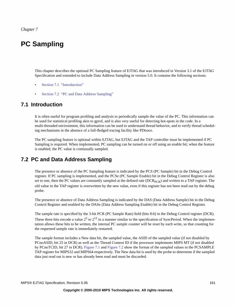
Chapter 7
MIPS® EJTAG Specification, Revision 5.06 161
Copyright © 2000-2010 MIPS Technologies Inc. All rights reserved.
PC Sampling
This chapter describes the optional PC Sampling feature of EJTAG that was introduced in Version 3.1 of the EJTAGSpecification and extended to include Data Address Sampling in version 5.0. It contains the following sections:
• Section 7.1 “Introduction”
• Section 7.2 “PC and Data Address Sampling”
7.1 Introduction
It is often useful for program profiling and analysis to periodically sample the value of the PC. This information canbe used for statistical profiling akin to gprof, and is also very useful for detecting hot-spots in the code. In amulti-threaded environment, this information can be used to understand thread behavior, and to verify thread schedul-ing mechanisms in the absence of a full-fledged tracing facility like PDtrace.
The PC sampling feature is optional within EJTAG, but EJTAG and the TAP controller must be implemented if PCSampling is required. When implemented, PC sampling can be turned on or off using an enable bit; when the featureis enabled, the PC value is continually sampled.
7.2 PC and Data Address Sampling
The presence or absence of the PC Sampling feature is indicated by the PCS (PC Sample) bit in the Debug Controlregister. If PC sampling is implemented, and the PCSe (PC Sample Enable) bit in the Debug Control Register is alsoset to one, then the PC values are constantly sampled at the defined rate (DCRPCR) and written to a TAP register. Theold value in the TAP register is overwritten by the new value, even if this register has not been read out by the debugprobe.
The presence or absence of Data Address Sampling is indicated by the DAS (Data Address Sample) bit in the DebugControl Register and enabled by the DASe (Data Address Sampling Enable) bit in the Debug Control Register.
The sample rate is specified by the 3-bit PCR (PC Sample Rate) field (bits 8:6) in the Debug Control register (DCR).
These three bits encode a value 25 to 212 in a manner similar to the specification of SyncPeriod. When the implemen-tation allows these bits to be written, the internal PC sample counter will be reset by each write, so that counting forthe requested sample rate is immediately restarted.
The sample format includes a New data bit, the sampled value, the ASID of the sampled value (if not disabled byPCnoASID, bit 25 in DCR) as well as the Thread Context ID if the processor implements MIPS MT (if not disabledby PCnoTCID, bit 27 in DCR). Figure 7.1 and Figure 7.2 show the format of the sampled values in the PCSAMPLETAP register for MIPS32 and MIPS64 respectively. The New data bit is used by the probe to determine if the sampleddata just read out is new or has already been read and must be discarded.
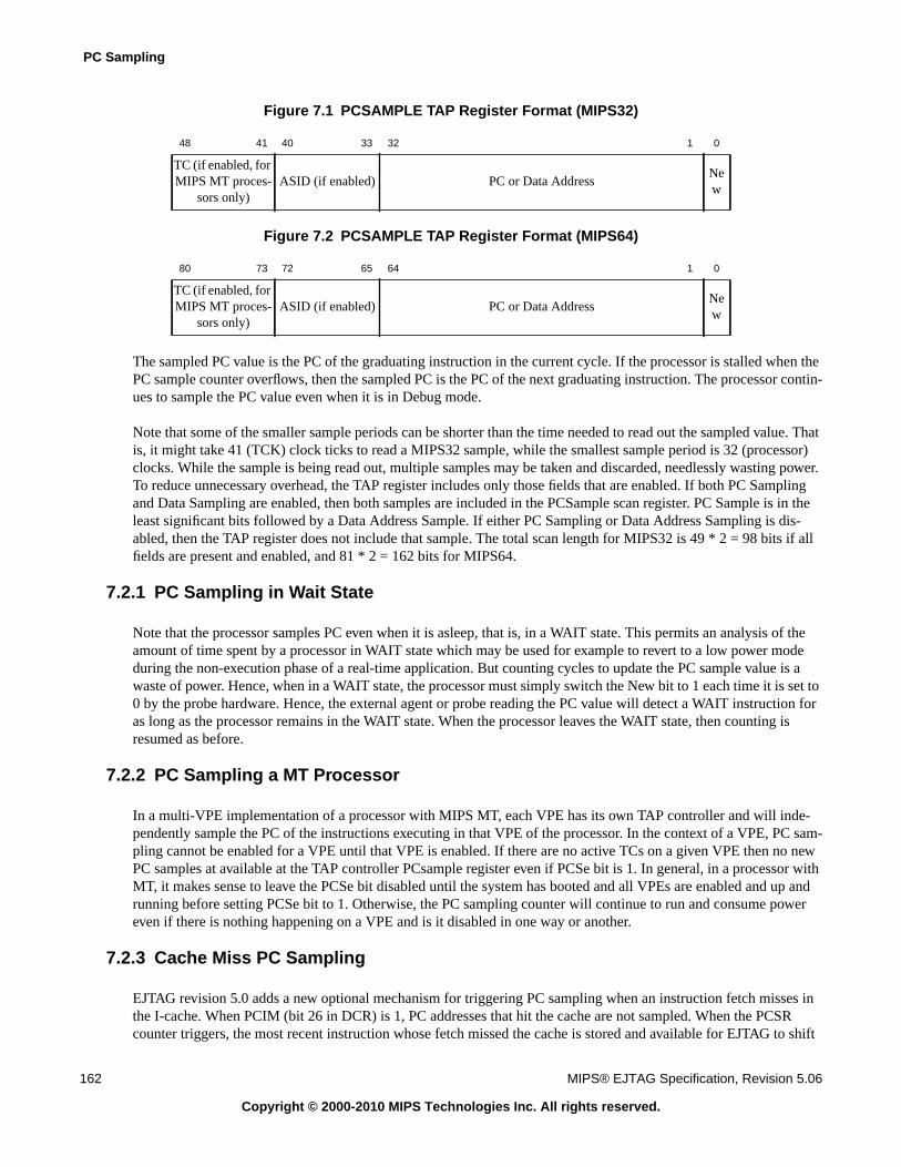
PC Sampling
162 MIPS® EJTAG Specification, Revision 5.06
Copyright © 2000-2010 MIPS Technologies Inc. All rights reserved.
Figure 7.1 PCSAMPLE TAP Register Format (MIPS32)
Figure 7.2 PCSAMPLE TAP Register Format (MIPS64)
The sampled PC value is the PC of the graduating instruction in the current cycle. If the processor is stalled when thePC sample counter overflows, then the sampled PC is the PC of the next graduating instruction. The processor contin-ues to sample the PC value even when it is in Debug mode.
Note that some of the smaller sample periods can be shorter than the time needed to read out the sampled value. Thatis, it might take 41 (TCK) clock ticks to read a MIPS32 sample, while the smallest sample period is 32 (processor)clocks. While the sample is being read out, multiple samples may be taken and discarded, needlessly wasting power.To reduce unnecessary overhead, the TAP register includes only those fields that are enabled. If both PC Samplingand Data Sampling are enabled, then both samples are included in the PCSample scan register. PC Sample is in theleast significant bits followed by a Data Address Sample. If either PC Sampling or Data Address Sampling is dis-abled, then the TAP register does not include that sample. The total scan length for MIPS32 is 49 * 2 = 98 bits if allfields are present and enabled, and 81 * 2 = 162 bits for MIPS64.
7.2.1 PC Sampling in Wait State
Note that the processor samples PC even when it is asleep, that is, in a WAIT state. This permits an analysis of theamount of time spent by a processor in WAIT state which may be used for example to revert to a low power modeduring the non-execution phase of a real-time application. But counting cycles to update the PC sample value is awaste of power. Hence, when in a WAIT state, the processor must simply switch the New bit to 1 each time it is set to0 by the probe hardware. Hence, the external agent or probe reading the PC value will detect a WAIT instruction foras long as the processor remains in the WAIT state. When the processor leaves the WAIT state, then counting isresumed as before.
7.2.2 PC Sampling a MT Processor
In a multi-VPE implementation of a processor with MIPS MT, each VPE has its own TAP controller and will inde-pendently sample the PC of the instructions executing in that VPE of the processor. In the context of a VPE, PC sam-pling cannot be enabled for a VPE until that VPE is enabled. If there are no active TCs on a given VPE then no newPC samples at available at the TAP controller PCsample register even if PCSe bit is 1. In general, in a processor withMT, it makes sense to leave the PCSe bit disabled until the system has booted and all VPEs are enabled and up andrunning before setting PCSe bit to 1. Otherwise, the PC sampling counter will continue to run and consume powereven if there is nothing happening on a VPE and is it disabled in one way or another.
7.2.3 Cache Miss PC Sampling
EJTAG revision 5.0 adds a new optional mechanism for triggering PC sampling when an instruction fetch misses inthe I-cache. When PCIM (bit 26 in DCR) is 1, PC addresses that hit the cache are not sampled. When the PCSRcounter triggers, the most recent instruction whose fetch missed the cache is stored and available for EJTAG to shift
48 41 40 33 32 1 0
TC (if enabled, forMIPS MT proces-
sors only)ASID (if enabled) PC or Data Address
New
80 73 72 65 64 1 0
TC (if enabled, forMIPS MT proces-
sors only)ASID (if enabled) PC or Data Address
New
7.2 PC and Data Address Sampling
MIPS® EJTAG Specification, Revision 5.06 163
Copyright © 2000-2010 MIPS Technologies Inc. All rights reserved.
out through PCSAMPLE. Over time, this collection mode results in an overall picture of the instruction cache behav-ior and can be used to increase performance by re-arranging code to minimize cache thrashing.
7.2.4 Data Address Sampling
EJTAG revision 5.0 extends the PC sampling mechanism to allow sampling of data (load and store) addresses. Thisfeature is enabled with DASe, bit 23 in the Debug Control register. When enabled, the PCSAMPLE scan registerincludes a data address sample. All load and store addresses can be captured, or they can be qualified using a databreakpoint trigger. DASQ=1 configures data sampling to record a data address only when it triggers data breakpoint0. To be used for Data Address Sampling qualification, data breakpoint 0 must be enabled using its TE (triggerenable) bit.
PCSR controls how often data addresses are sampled. When the PCSR counter triggers, the most recent load/storeaddress generated is accepted and made available to shift out through PCSAMPLE.

PC Sampling
164 MIPS® EJTAG Specification, Revision 5.06
Copyright © 2000-2010 MIPS Technologies Inc. All rights reserved.
Chapter 8
MIPS® EJTAG Specification, Revision 5.06 165
Copyright © 2000-2010 MIPS Technologies Inc. All rights reserved.
Fast Debug Channel
EJTAG version 5.0 adds an optional Fast Debug Channel (FDC) mechanism for higher bandwidth data transfersbetween a debug host/probe and a target. The existing FASTDATA mechanism was designed to make data transfersmore efficient in terms of TAP bandwidth utilization. However, the FASTDATA mechanism causes the target CPUto block on every fastdata memory access, preventing it from executing non-debug instructions and making the datatransfer intrusive to the program under debug. The FDC mechanism allows the user to set up a data transfer, and thenresume normal operation. The data transfer occurs in the background, and the target CPU can either choose to checkthe status of the transfer periodically, or it can choose to be interrupted at the end of the transfer. The FDC mecha-nism adds several architectural components to EJTAG state. The rest of this chapter describes these components andthe usage of FDC in more detail.
8.1 Overview
The FDC mechanism adds two First In First Out (FIFO) structures that are mapped to the target CPU’s physicaladdress map. The probe uses the new FDC TAP instruction to access these FIFOs, while the CPU accesses themusing memory accesses. To transfer data out of the core, the CPU writes one or more pieces of data to the transmitFIFO. At this time, the CPU can resume doing other work. An external probe would examine the status of the trans-mit FIFO periodically, and if there is data to be read, the probe starts to receive data from the FIFO, one entry at atime. When all data from the FIFO has been drained, the probe goes back to waiting for the CPU to write more data.The CPU can either choose to be informed of the empty transmit FIFO via an interrupt, or it can choose to periodi-cally check the status. Receiving data works in a similar manner, that is, the probe writes to the receive FIFO. At thattime, the CPU is either interrupted, or learns of the event by polling a status bit. The CPU can then do load accesses tothe receive FIFO and receive data being sent to it by the probe.
The primary advantage of FDC is that it does not require the CPU to be blocked when the probe is reading or writingthe data transfer FIFOs. This significantly reduces the CPU overhead, and makes the data transfer far less intrusive tothe code executing on the CPU.
8.2 FDC Features
The FDC memory-mapped registers are located in the common device memory map (CDMM) region. FDC has adevice ID of 0xFD.
8.2.1 Fast Debug Interrupt
The FDC block can generate an interrupt to isgnal the CPU that data is available to receive or that space is availableto send data, If interrupts are enabled, they will be generated based on the occupancy of the receive and transmitFIFOs. Enabling the receive interrupt also enables the generation of an interrupt from the probe using a special datavalue. Note that this is a regular interrupt, not a debug interrupt.
The FDC Configuration Register (see Section 8.3.2 “FDC Configuration (FDCFG) Register (Offset 0x8)”) includesfields for enabling and setting the threshold for generating each interrupt. These can be set to match the desiredbehavior as follows:
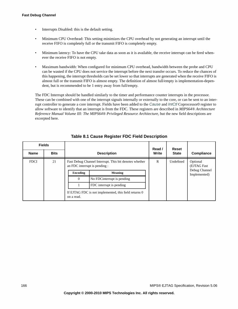
Fast Debug Channel
166 MIPS® EJTAG Specification, Revision 5.06
Copyright © 2000-2010 MIPS Technologies Inc. All rights reserved.
• Interrupts Disabled: this is the default setting.
• Minimum CPU Overhead: This setting minimizes the CPU overhead by not generating an interrupt until thereceive FIFO is completely full or the transmit FIFO is completely empty.
• Minimum latency: To have the CPU take data as soon as it is available, the receive interrupt can be fired when-ever the receive FIFO is not empty.
• Maximum bandwidth: When configured for minimum CPU overhead, bandwidth between the probe and CPUcan be wasted if the CPU does not service the interrupt before the next transfer occurs. To reduce the chances ofthis happening, the interrupt thresholds can be set lower so that interrupts are generated when the receive FIFO isalmost full or the transmit FIFO is almost empty. The definition of almost full/empty is implementation-depen-dent, but is recommended to be 1 entry away from full/empty.
The FDC Interrupt should be handled similarly to the timer and performance counter interrupts in the processor.These can be combined with one of the interrupt signals internally or externally to the core, or can be sent to an inter-rupt controller to generate a core interrupt. Fields have been added to the Cause and IntCtl Coprocessor0 register toallow software to identify that an interrupt is from the FDC. These registers are described in MIPS64® ArchitectureReference Manual Volume III: The MIPS64® Privileged Resource Architecture, but the new field descriptions areexcerpted here.
Table 8.1 Cause Register FDC Field Description
Fields
DescriptionRead /Write
ResetState ComplianceName Bits
FDCI 21 Fast Debug Channel Interrupt. This bit denotes whetheran FDC interrupt is pending :
If EJTAG FDC is not implemented, this field returns 0on a read.
R Undefined Optional(EJTAG FastDebug ChannelImplemented)Encoding Meaning
0 No FDCinterrupt is pending
1 FDC interrupt is pending
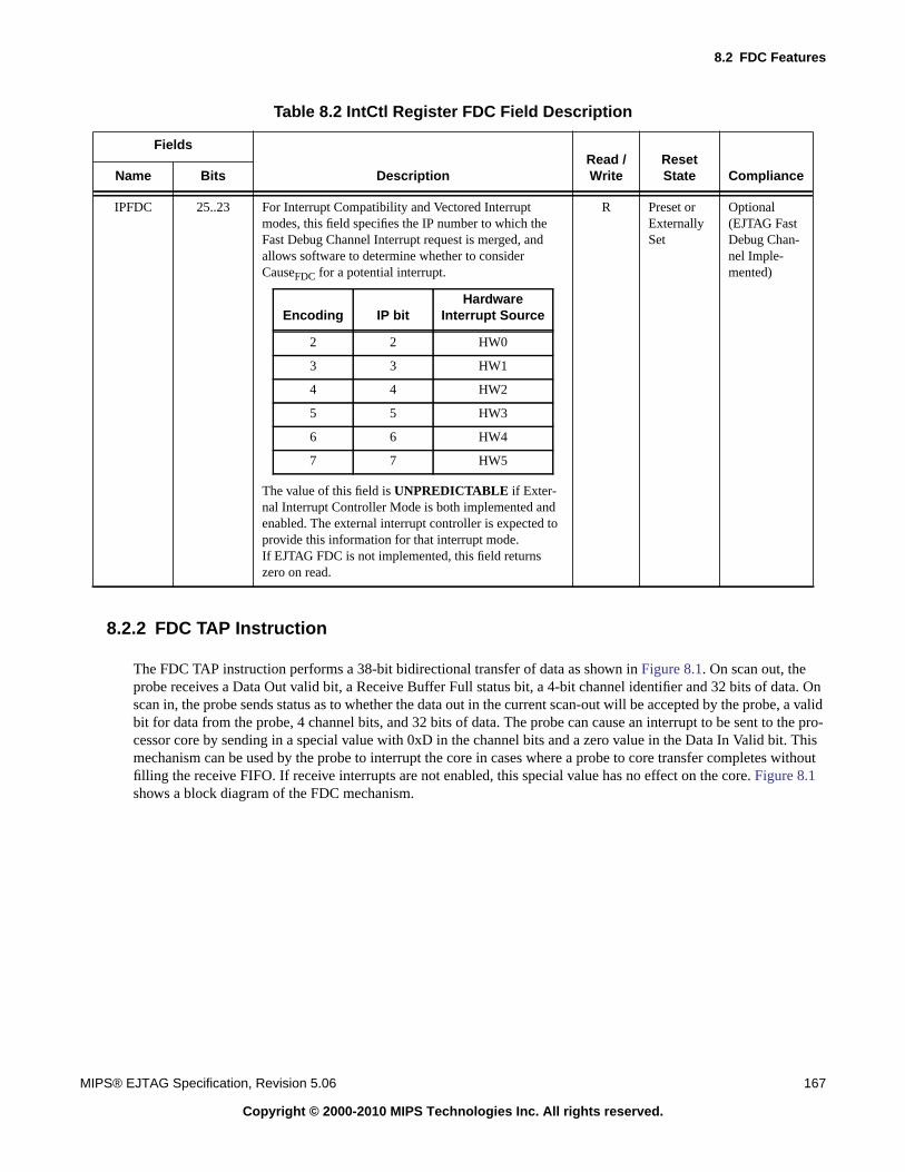
8.2 FDC Features
MIPS® EJTAG Specification, Revision 5.06 167
Copyright © 2000-2010 MIPS Technologies Inc. All rights reserved.
8.2.2 FDC TAP Instruction
The FDC TAP instruction performs a 38-bit bidirectional transfer of data as shown in Figure 8.1. On scan out, theprobe receives a Data Out valid bit, a Receive Buffer Full status bit, a 4-bit channel identifier and 32 bits of data. Onscan in, the probe sends status as to whether the data out in the current scan-out will be accepted by the probe, a validbit for data from the probe, 4 channel bits, and 32 bits of data. The probe can cause an interrupt to be sent to the pro-cessor core by sending in a special value with 0xD in the channel bits and a zero value in the Data In Valid bit. Thismechanism can be used by the probe to interrupt the core in cases where a probe to core transfer completes withoutfilling the receive FIFO. If receive interrupts are not enabled, this special value has no effect on the core. Figure 8.1shows a block diagram of the FDC mechanism.
Table 8.2 IntCtl Register FDC Field Description
Fields
DescriptionRead /Write
ResetState ComplianceName Bits
IPFDC 25..23 For Interrupt Compatibility and Vectored Interruptmodes, this field specifies the IP number to which theFast Debug Channel Interrupt request is merged, andallows software to determine whether to considerCauseFDC for a potential interrupt.
The value of this field is UNPREDICTABLE if Exter-nal Interrupt Controller Mode is both implemented andenabled. The external interrupt controller is expected toprovide this information for that interrupt mode.If EJTAG FDC is not implemented, this field returnszero on read.
R Preset orExternallySet
Optional(EJTAG FastDebug Chan-nel Imple-mented)
Encoding IP bitHardware
Interrupt Source
2 2 HW0
3 3 HW1
4 4 HW2
5 5 HW3
6 6 HW4
7 7 HW5
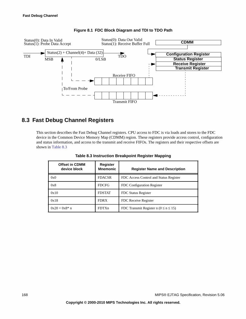
Fast Debug Channel
168 MIPS® EJTAG Specification, Revision 5.06
Copyright © 2000-2010 MIPS Technologies Inc. All rights reserved.
Figure 8.1 FDC Block Diagram and TDI to TDO Path
8.3 Fast Debug Channel Registers
This section describes the Fast Debug Channel registers. CPU access to FDC is via loads and stores to the FDCdevice in the Common Device Memory Map (CDMM) region. These registers provide access control, configurationand status information, and access to the transmit and receive FIFOs. The registers and their respective offsets areshown in Table 8.3
Table 8.3 Instruction Breakpoint Register Mapping
Offset in CDMMdevice block
RegisterMnemonic Register Name and Description
0x0 FDACSR FDC Access Control and Status Register
0x8 FDCFG FDC Configuration Register
0x10 FDSTAT FDC Status Register
0x18 FDRX FDC Receive Register
0x20 + 0x8* n FDTXn FDC Transmit Register n (0 ≤ n ≤ 15)
Transmit FIFO
Receive FIFO
To/From Probe
TDI TDOStatus(2) + Channel(4)+ Data (32)
0/LSBMSB
CDMM
Configuration RegisterStatus RegisterReceive RegisterTransmit Register
Status(0): Data In ValidStatus(1): Probe Data Accept
Status(0): Data Out ValidStatus(1): Receive Buffer Full
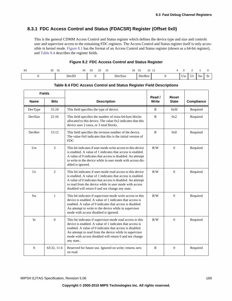
8.3 Fast Debug Channel Registers
MIPS® EJTAG Specification, Revision 5.06 169
Copyright © 2000-2010 MIPS Technologies Inc. All rights reserved.
8.3.1 FDC Access Control and Status (FDACSR) Register (Offset 0x0)
This is the general CDMM Access Control and Status register which defines the device type and size and controlsuser and supervisor access to the remaining FDC registers. The Access Control and Status register itself is only acces-sible in kernel mode. Figure 8.1 has the format of an Access Control and Status register (shown as a 64-bit register),and Table 8.4 describes the register fields.
Figure 8.2 FDC Access Control and Status Register
63 32 31 24 23 22 21 16 15 12 11 4 3 2 1 0
0 DevID 0 DevSize DevRev 0 Uw Ur Sw Sr
Table 8.4 FDC Access Control and Status Register Field Descriptions
Fields
DescriptionRead /Write
ResetState ComplianceName Bits
DevType 31:24 This field specifies the type of device. R 0xfd Required
DevSize 21:16 This field specifies the number of extra 64-byte blocksallocated to this device. The value 0x2 indicates that thisdevice uses 2 extra, or 3 total blocks.
R 0x2 Required
DevRev 15:12 This field specifies the revision number of the device.The value 0x0 indicates that this is the initial version ofFDC
R 0x0 Required
Uw 3 This bit indicates if user-mode write access to this deviceis enabled. A value of 1 indicates that access is enabled.A value of 0 indicates that access is disabled. An attemptto write to the device while in user mode with access dis-abled is ignored.
R/W 0 Required
Ur 2 This bit indicates if user-mode read access to this deviceis enabled. A value of 1 indicates that access is enabled.A value of 0 indicates that access is disabled. An attemptto read from the device while in user mode with accessdisabled will return 0 and not change any state.
R/W 0 Required
Sw 1 This bit indicates if supervisor-mode write access to thisdevice is enabled. A value of 1 indicates that access isenabled. A value of 0 indicates that access is disabled.An attempt to write to the device while in supervisormode with access disabled is ignored.
R/W 0 Required
Sr 0 This bit indicates if supervisor-mode read access to thisdevice is enabled. A value of 1 indicates that access isenabled. A value of 0 indicates that access is disabled.An attempt to read from the device while in supervisormode with access disabled will return 0 and not changeany state..
R/W 0 Required
0 63:32, 11:4 Reserved for future use. Ignored on write; returns zeroon read.
R 0 Required
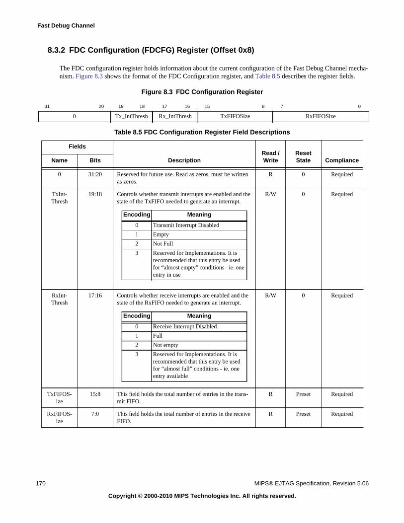
Fast Debug Channel
170 MIPS® EJTAG Specification, Revision 5.06
Copyright © 2000-2010 MIPS Technologies Inc. All rights reserved.
8.3.2 FDC Configuration (FDCFG) Register (Offset 0x8)
The FDC configuration register holds information about the current configuration of the Fast Debug Channel mecha-nism. Figure 8.3 shows the format of the FDC Configuration register, and Table 8.5 describes the register fields.
Figure 8.3 FDC Configuration Register
31 20 19 18 17 16 15 8 7 0
0 Tx_IntThresh Rx_IntThresh TxFIFOSize RxFIFOSize
Table 8.5 FDC Configuration Register Field Descriptions
Fields
DescriptionRead /Write
ResetState ComplianceName Bits
0 31:20 Reserved for future use. Read as zeros, must be writtenas zeros.
R 0 Required
TxInt-Thresh
19:18 Controls whether transmit interrupts are enabled and thestate of the TxFIFO needed to generate an interrupt.
R/W 0 Required
RxInt-Thresh
17:16 Controls whether receive interrupts are enabled and thestate of the RxFIFO needed to generate an interrupt.
R/W 0 Required
TxFIFOS-ize
15:8 This field holds the total number of entries in the trans-mit FIFO.
R Preset Required
RxFIFOS-ize
7:0 This field holds the total number of entries in the receiveFIFO.
R Preset Required
Encoding Meaning
0 Transmit Interrupt Disabled
1 Empty
2 Not Full
3 Reserved for Implementations. It isrecommended that this entry be usedfor “almost empty” conditions - ie. oneentry in use
Encoding Meaning
0 Receive Interrupt Disabled
1 Full
2 Not empty
3 Reserved for Implementations. It isrecommended that this entry be usedfor “almost full” conditions - ie. oneentry available
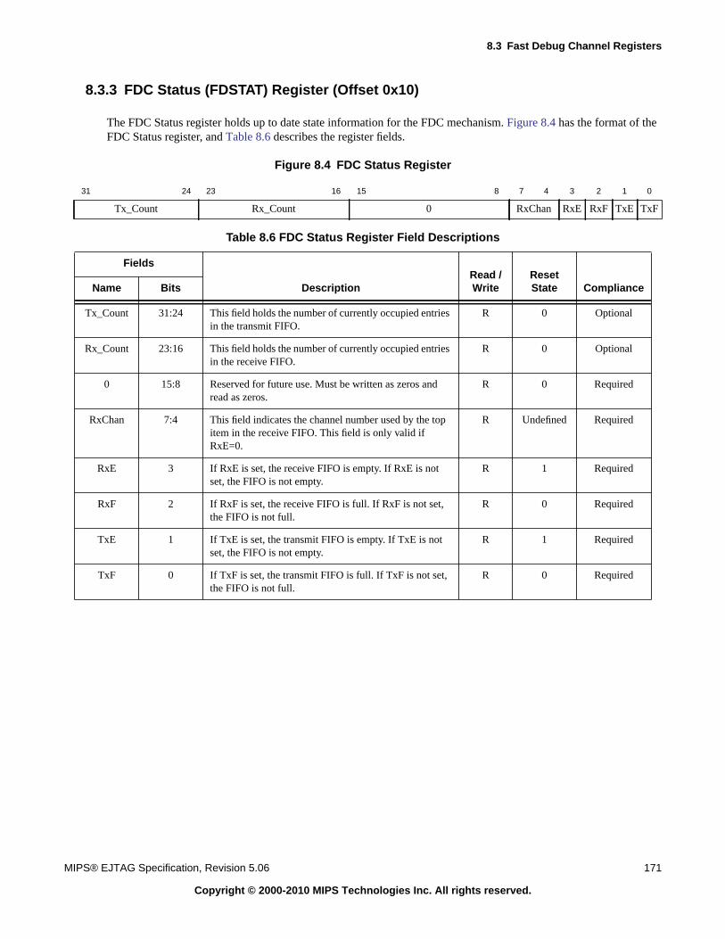
8.3 Fast Debug Channel Registers
MIPS® EJTAG Specification, Revision 5.06 171
Copyright © 2000-2010 MIPS Technologies Inc. All rights reserved.
8.3.3 FDC Status (FDSTAT) Register (Offset 0x10)
The FDC Status register holds up to date state information for the FDC mechanism. Figure 8.4 has the format of theFDC Status register, and Table 8.6 describes the register fields.
Figure 8.4 FDC Status Register
31 24 23 16 15 8 7 4 3 2 1 0
Tx_Count Rx_Count 0 RxChan RxE RxF TxE TxF
Table 8.6 FDC Status Register Field Descriptions
Fields
DescriptionRead /Write
ResetState ComplianceName Bits
Tx_Count 31:24 This field holds the number of currently occupied entriesin the transmit FIFO.
R 0 Optional
Rx_Count 23:16 This field holds the number of currently occupied entriesin the receive FIFO.
R 0 Optional
0 15:8 Reserved for future use. Must be written as zeros andread as zeros.
R 0 Required
RxChan 7:4 This field indicates the channel number used by the topitem in the receive FIFO. This field is only valid ifRxE=0.
R Undefined Required
RxE 3 If RxE is set, the receive FIFO is empty. If RxE is notset, the FIFO is not empty.
R 1 Required
RxF 2 If RxF is set, the receive FIFO is full. If RxF is not set,the FIFO is not full.
R 0 Required
TxE 1 If TxE is set, the transmit FIFO is empty. If TxE is notset, the FIFO is not empty.
R 1 Required
TxF 0 If TxF is set, the transmit FIFO is full. If TxF is not set,the FIFO is not full.
R 0 Required
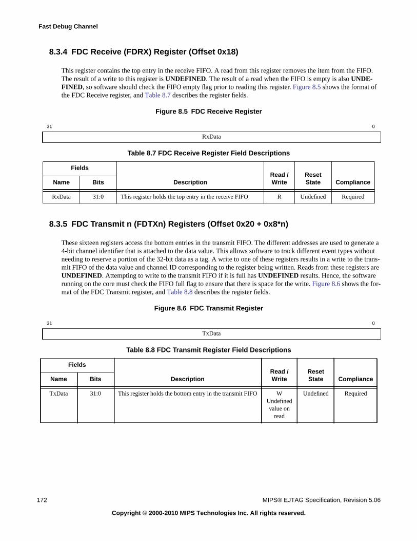
Fast Debug Channel
172 MIPS® EJTAG Specification, Revision 5.06
Copyright © 2000-2010 MIPS Technologies Inc. All rights reserved.
8.3.4 FDC Receive (FDRX) Register (Offset 0x18)
This register contains the top entry in the receive FIFO. A read from this register removes the item from the FIFO.The result of a write to this register is UNDEFINED. The result of a read when the FIFO is empty is also UNDE-FINED, so software should check the FIFO empty flag prior to reading this register. Figure 8.5 shows the format ofthe FDC Receive register, and Table 8.7 describes the register fields.
Figure 8.5 FDC Receive Register
8.3.5 FDC Transmit n (FDTXn) Registers (Offset 0x20 + 0x8*n)
These sixteen registers access the bottom entries in the transmit FIFO. The different addresses are used to generate a4-bit channel identifier that is attached to the data value. This allows software to track different event types withoutneeding to reserve a portion of the 32-bit data as a tag. A write to one of these registers results in a write to the trans-mit FIFO of the data value and channel ID corresponding to the register being written. Reads from these registers areUNDEFINED. Attempting to write to the transmit FIFO if it is full has UNDEFINED results. Hence, the softwarerunning on the core must check the FIFO full flag to ensure that there is space for the write. Figure 8.6 shows the for-mat of the FDC Transmit register, and Table 8.8 describes the register fields.
Figure 8.6 FDC Transmit Register
31 0
RxData
Table 8.7 FDC Receive Register Field Descriptions
Fields
DescriptionRead /Write
ResetState ComplianceName Bits
RxData 31:0 This register holds the top entry in the receive FIFO R Undefined Required
31 0
TxData
Table 8.8 FDC Transmit Register Field Descriptions
Fields
DescriptionRead /Write
ResetState ComplianceName Bits
TxData 31:0 This register holds the bottom entry in the transmit FIFO WUndefinedvalue on
read
Undefined Required
Chapter 9
MIPS® EJTAG Specification, Revision 5.06 173
Copyright © 2000-2010 MIPS Technologies Inc. All rights reserved.
On-Chip Interfaces
This chapter covers issues regarding implementation of a processor on a chip with respect to hook-up of the EJTAGTAP and DINT interfaces. It contains the following sections:
• Section 9.1 “Connecting Unused EJTAG Test Access Port and Debug Interrupt Signals”
• Section 9.2 “Optional TRST* Pin”
• Section 9.3 “Input Buffers with Pull-Up/Down and Output Drivers for Chip Pins”
• Section 9.4 “Connecting Multi-Core Test Access Port (TAP) Controllers”
9.1 Connecting Unused EJTAG Test Access Port and Debug Interrupt Sig-nals
If the EJTAG capabilities provided through the Test Access Port (TAP) and Debug Interrupt (DINT) signals on a pro-cessor core are unused when the processor core is implemented on a chip, then TRST* is tied to low (if TRST* ispresent on the core) and the remaining input signals TCK, TMS, TDI, and DINT must be tied to a constant value,either high or low. The output signal TDO should be left unconnected.
9.2 Optional TRST* Pin
The TRST* signal to the TAP is optional, and need not be provided as a pin on the chip for a processor implementingthe EJTAG TAP.
If a TRST* chip pin is not provided, then a TAP reset like the one provided when TRST* is asserted (low) must beapplied to the TAP at power-up, for example, through a power-up reset circuit on the chip. This power-up TAP resetmust be finished after the time TVIOrise (see Section 10.2.4 on page 181).
If a TRST* chip pin is provided, then the power-up TAP reset is applied by a pull-down resistor, because the probewill not drive TRST* at power-up.
9.3 Input Buffers with Pull-Up/Down and Output Drivers for Chip Pins
If an input buffer with an integrated pull-up resistor is used for the TRST* chip pin, then its resistor value must besufficiently large that it is overruled by the external pull-down resistor on the PCB, so a well-defined logical level ispresent on the TRST* pin (see Section 10.5.1 on page 183 for more information).
Observe the additional rules described in the IEEE Std. 1149.1 specification, if the same TAP is used for JTAGboundary scan also.
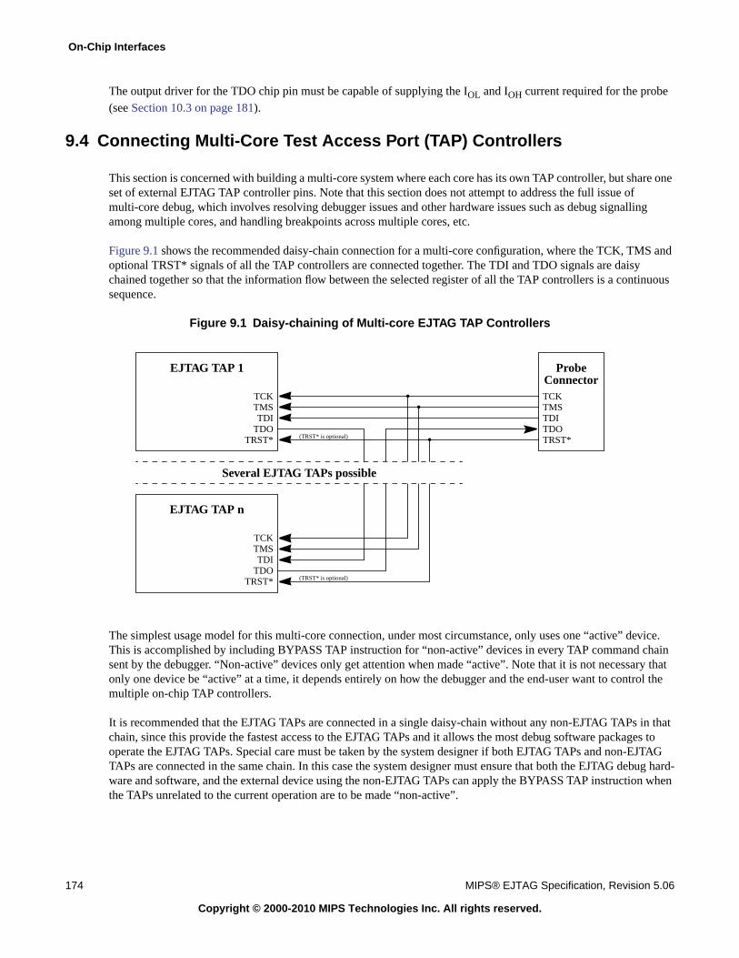
On-Chip Interfaces
174 MIPS® EJTAG Specification, Revision 5.06
Copyright © 2000-2010 MIPS Technologies Inc. All rights reserved.
The output driver for the TDO chip pin must be capable of supplying the IOL and IOH current required for the probe(see Section 10.3 on page 181).
9.4 Connecting Multi-Core Test Access Port (TAP) Controllers
This section is concerned with building a multi-core system where each core has its own TAP controller, but share oneset of external EJTAG TAP controller pins. Note that this section does not attempt to address the full issue ofmulti-core debug, which involves resolving debugger issues and other hardware issues such as debug signallingamong multiple cores, and handling breakpoints across multiple cores, etc.
Figure 9.1 shows the recommended daisy-chain connection for a multi-core configuration, where the TCK, TMS andoptional TRST* signals of all the TAP controllers are connected together. The TDI and TDO signals are daisychained together so that the information flow between the selected register of all the TAP controllers is a continuoussequence.
Figure 9.1 Daisy-chaining of Multi-core EJTAG TAP Controllers
The simplest usage model for this multi-core connection, under most circumstance, only uses one “active” device.This is accomplished by including BYPASS TAP instruction for “non-active” devices in every TAP command chainsent by the debugger. “Non-active” devices only get attention when made “active”. Note that it is not necessary thatonly one device be “active” at a time, it depends entirely on how the debugger and the end-user want to control themultiple on-chip TAP controllers.
It is recommended that the EJTAG TAPs are connected in a single daisy-chain without any non-EJTAG TAPs in thatchain, since this provide the fastest access to the EJTAG TAPs and it allows the most debug software packages tooperate the EJTAG TAPs. Special care must be taken by the system designer if both EJTAG TAPs and non-EJTAGTAPs are connected in the same chain. In this case the system designer must ensure that both the EJTAG debug hard-ware and software, and the external device using the non-EJTAG TAPs can apply the BYPASS TAP instruction whenthe TAPs unrelated to the current operation are to be made “non-active”.
Probe
TCKTMS
TDOTDI
TRST*
ConnectorTCKTMS
TDOTDI
TRST*
EJTAG TAP 1
(TRST* is optional)
TCKTMS
TDOTDI
TRST*
EJTAG TAP n
(TRST* is optional)
Several EJTAG TAPs possible
Chapter 10
MIPS® EJTAG Specification, Revision 5.06 175
Copyright © 2000-2010 MIPS Technologies Inc. All rights reserved.
Off-Chip and Probe Interfaces
This chapter outlines the requirements for the target system chip and probe interfaces to make them compatible. Thischapter contains the following sections:
• Section 10.1 “Logical Signals”
• Section 10.2 “AC Timing Characteristics”
• Section 10.3 “DC Electrical Characteristics”
• Section 10.4 “Mechanical Connector”
• Section 10.5 “Target System PCB Design”
• Section 10.6 “Probe Requirements and Recommendations”
The off-chip interface forms the connection from the chip over the target system PCB and to the probe connector,thereby allowing the probe to connect to the target processor. The probe connection is optional in the target system.
The probe signals are described with respect to logical functionality, timing behavior, electrical characteristics, andconnector and PCB design. Comments are also added with respect to probe functionality.
The descriptions in this chapter only cover issues related to EJTAG use of the Test Access Port (TAP). Issues relatedto reuse of the same TAP on a chip, for example, for JTAG boundary scan, are not covered.
10.1 Logical Signals
This section describes the EJTAG signals categorized according to functionality:
• Test Access Port: TCK, TMS, TDI, TDO, and TRST* (optional TRST*)
• Debug Interrupt: DINT (optional)
• System reset (reset or soft reset): RST*
• Return TCK: RTCK (optional)
• Voltage Sense for I/O: VIO
Figure 10.1 shows the signal flow between the chip, target system PCB, and Probe.
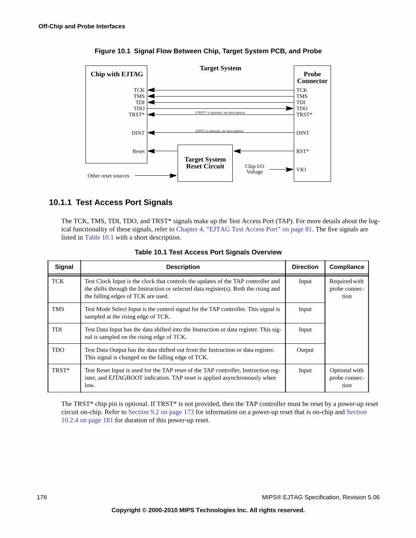
Off-Chip and Probe Interfaces
176 MIPS® EJTAG Specification, Revision 5.06
Copyright © 2000-2010 MIPS Technologies Inc. All rights reserved.
Figure 10.1 Signal Flow Between Chip, Target System PCB, and Probe
10.1.1 Test Access Port Signals
The TCK, TMS, TDI, TDO, and TRST* signals make up the Test Access Port (TAP). For more details about the log-ical functionality of these signals, refer to Chapter 4, “EJTAG Test Access Port” on page 81. The five signals arelisted in Table 10.1 with a short description.
The TRST* chip pin is optional. If TRST* is not provided, then the TAP controller must be reset by a power-up resetcircuit on-chip. Refer to Section 9.2 on page 173 for information on a power-up reset that is on-chip and Section10.2.4 on page 181 for duration of this power-up reset.
Table 10.1 Test Access Port Signals Overview
Signal Description Direction Compliance
TCK Test Clock Input is the clock that controls the updates of the TAP controller andthe shifts through the Instruction or selected data register(s). Both the rising andthe falling edges of TCK are used.
Input Required withprobe connec-
tion
TMS Test Mode Select Input is the control signal for the TAP controller. This signal issampled at the rising edge of TCK.
Input
TDI Test Data Input has the data shifted into the Instruction or data register. This sig-nal is sampled on the rising edge of TCK.
Input
TDO Test Data Output has the data shifted out from the Instruction or data register.This signal is changed on the falling edge of TCK.
Output
TRST* Test Reset Input is used for the TAP reset of the TAP controller, Instruction reg-ister, and EJTAGBOOT indication. TAP reset is applied asynchronously whenlow.
Input Optional withprobe connec-
tion
Target System
Probe
TCKTMS
TDOTDI
TRST*
DINT
RST*
VIO
ConnectorTCKTMS
TDOTDI
TRST*
DINT
Chip with EJTAG
Reset
Other reset sources
(TRST* is optional, see description)
Chip I/OVoltage
(DINT is optional, see description)
Reset Circuit
Target System
10.1 Logical Signals
MIPS® EJTAG Specification, Revision 5.06 177
Copyright © 2000-2010 MIPS Technologies Inc. All rights reserved.
10.1.2 Debug Interrupt Signal
The Debug Interrupt (DINT) signal allows the probe to request the CPU to take a debug exception. Table 10.2 brieflydefines this signal.
The DINT signal from the probe is optional. The DINTsup bit indicates whether or not the DINT signal is imple-mented. Refer to Section 4.5.2 on page 90 for more information on DINTsup. The debug interrupt request isdescribed in Section 2.3.10 on page 49.
10.1.3 System Reset Signal
The System Reset (RST*) signal from the probe is required to generate a reset of the target board. It is recommendedthat assertion of RST* results in a (hard) reset of the processor, but it is allowed to generate a soft reset. Table 10.3briefly describes the RST* signal.
The probe controls the RST* via an open-collector (OC) output. Thus RST* is actively driven low when asserted(low), but is 3-stated when deasserted (high).
10.1.4 Return Test Clock Input
The Voltage sense for I/O (VIO) indicates target power is applied and voltage levels are present at the probe I/O con-nections. Table 10.5 briefly describes the VIO signal.
This is useful when for example, a hardware emulator used with the target core wants to hook up an EJTAG probe fordebugging. The hardware emulator starts and stops its system clock and needs the debug probe to pause any JTAGoperations during that time. This can be achieved by the addition of a return TCK signal which is an output from thetarget chip to the probe and is a mirror of the probe’s TCK input after clocking with the system clock. The probe can
Table 10.2 Debug Interrupt Signal Overview
Signal Description Direction Compliance
DINT A debug interrupt is requested when DINT goes from low to high. The CPU isallowed to synchronize this signal to the CPU clock before detecting its risingedge, if this is possible with respect to the minimum pulse width indicated inSection 10.2.2 on page 180. The request is ignored if the CPU is already inDebug Mode.
Input Optional withEJTAG TAP
Table 10.3 System Reset Signal Overview
Signal Description Direction Compliance
RST* RST* is the system reset of the target board. When the probe asserts RST* low,the result is either a reset (recommended) or soft reset of the processor.No reset is applied when the RST* is undriven (3-stated from the probe).
Input Required withprobe connec-
tion
Table 10.4 Voltage Sense for I/O Signal Overview
Signal Description Direction Compliance
RTCK This return TCK signal to the JTAG connector allows the target chip underdebug to mirror the start and stop of its system clock to correspond to start andstop of the debug probe.
Input Optional withprobe connec-
tion
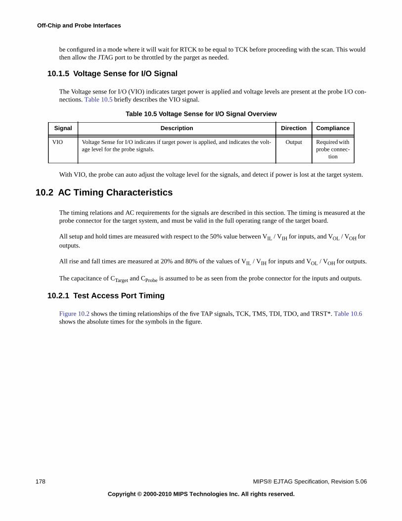
Off-Chip and Probe Interfaces
178 MIPS® EJTAG Specification, Revision 5.06
Copyright © 2000-2010 MIPS Technologies Inc. All rights reserved.
be configured in a mode where it will wait for RTCK to be equal to TCK before proceeding with the scan. This wouldthen allow the JTAG port to be throttled by the parget as needed.
10.1.5 Voltage Sense for I/O Signal
The Voltage sense for I/O (VIO) indicates target power is applied and voltage levels are present at the probe I/O con-nections. Table 10.5 briefly describes the VIO signal.
With VIO, the probe can auto adjust the voltage level for the signals, and detect if power is lost at the target system.
10.2 AC Timing Characteristics
The timing relations and AC requirements for the signals are described in this section. The timing is measured at theprobe connector for the target system, and must be valid in the full operating range of the target board.
All setup and hold times are measured with respect to the 50% value between VIL / VIH for inputs, and VOL / VOH foroutputs.
All rise and fall times are measured at 20% and 80% of the values of VIL / VIH for inputs and VOL / VOH for outputs.
The capacitance of CTarget and CProbe is assumed to be as seen from the probe connector for the inputs and outputs.
10.2.1 Test Access Port Timing
Figure 10.2 shows the timing relationships of the five TAP signals, TCK, TMS, TDI, TDO, and TRST*. Table 10.6shows the absolute times for the symbols in the figure.
Table 10.5 Voltage Sense for I/O Signal Overview
Signal Description Direction Compliance
VIO Voltage Sense for I/O indicates if target power is applied, and indicates the volt-age level for the probe signals.
Output Required withprobe connec-
tion
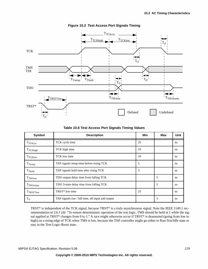
10.2 AC Timing Characteristics
MIPS® EJTAG Specification, Revision 5.06 179
Copyright © 2000-2010 MIPS Technologies Inc. All rights reserved.
Figure 10.2 Test Access Port Signals Timing
TRST* is independent of the TCK signal, because TRST* is a truly asynchronous signal. Note the IEEE 1149.1 rec-ommendation in 3.6.1 (d): “To ensure deterministic operation of the test logic, TMS should be held at 1 while the sig-nal applied at TRST* changes from 0 to 1.” A race might otherwise occur if TRST* is deasserted (going from low tohigh) on a rising edge of TCK when TMS is low, because the TAP controller might go either to Run-Test/Idle state orstay in the Test-Logic-Reset state.
Table 10.6 Test Access Port Signals Timing Values
Symbol Description Min Max Unit
TTCKcyc TCK cycle time 25 ns
TTCKhigh TCK high time 10 ns
TTCKlow TCK low time 10 ns
TTsetup TAP signals setup time before rising TCK 5 ns
TThold TAP signals hold time after rising TCK 3 ns
TTDOout TDO output delay time from falling TCK 5 ns
TTDOzstate TDO 3-state delay time from falling TCK 5 ns
TTRST*low TRST* low time 25 ns
Trf TAP signals rise / fall time, all input and output 3 ns
TCK
TTCKcyc
TTCKhigh TTCKlow
TRST*
TTRST*low
TMSTDI
TTDOout
TThold
TTDOzstate
TDO
TTsetup
UndefinedDefined
Trf
Trf
Trf
Trf
Trf
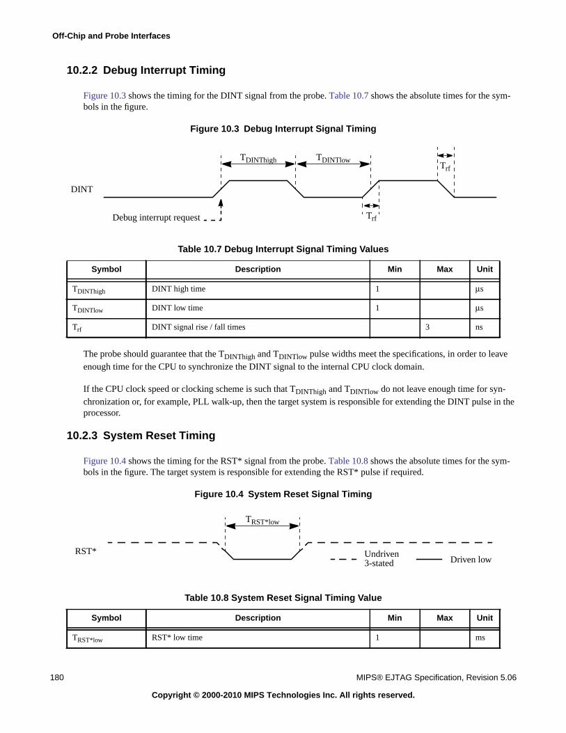
Off-Chip and Probe Interfaces
180 MIPS® EJTAG Specification, Revision 5.06
Copyright © 2000-2010 MIPS Technologies Inc. All rights reserved.
10.2.2 Debug Interrupt Timing
Figure 10.3 shows the timing for the DINT signal from the probe. Table 10.7 shows the absolute times for the sym-bols in the figure.
Figure 10.3 Debug Interrupt Signal Timing
The probe should guarantee that the TDINThigh and TDINTlow pulse widths meet the specifications, in order to leaveenough time for the CPU to synchronize the DINT signal to the internal CPU clock domain.
If the CPU clock speed or clocking scheme is such that TDINThigh and TDINTlow do not leave enough time for syn-chronization or, for example, PLL walk-up, then the target system is responsible for extending the DINT pulse in theprocessor.
10.2.3 System Reset Timing
Figure 10.4 shows the timing for the RST* signal from the probe. Table 10.8 shows the absolute times for the sym-bols in the figure. The target system is responsible for extending the RST* pulse if required.
Figure 10.4 System Reset Signal Timing
Table 10.7 Debug Interrupt Signal Timing Values
Symbol Description Min Max Unit
TDINThigh DINT high time 1 µs
TDINTlow DINT low time 1 µs
Trf DINT signal rise / fall times 3 ns
Table 10.8 System Reset Signal Timing Value
Symbol Description Min Max Unit
TRST*low RST* low time 1 ms
DINT
TDINThigh TDINTlowTrf
TrfDebug interrupt request
RST*
TRST*low
Driven lowUndriven3-stated
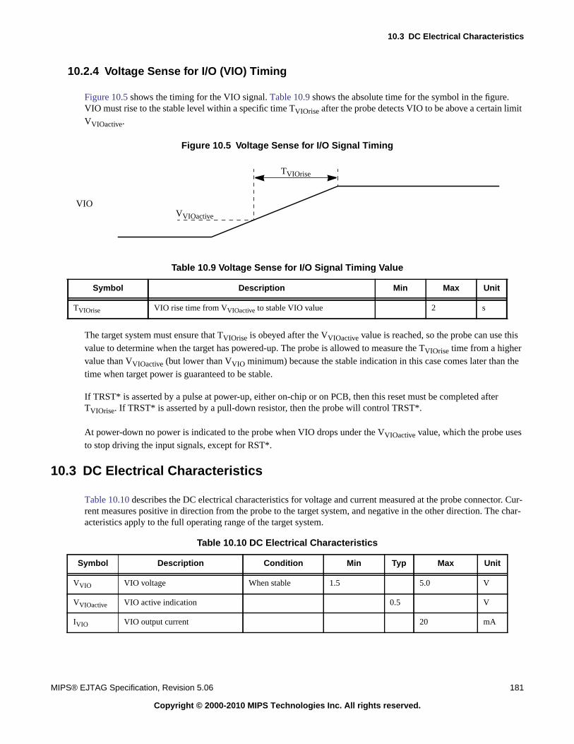
10.3 DC Electrical Characteristics
MIPS® EJTAG Specification, Revision 5.06 181
Copyright © 2000-2010 MIPS Technologies Inc. All rights reserved.
10.2.4 Voltage Sense for I/O (VIO) Timing
Figure 10.5 shows the timing for the VIO signal. Table 10.9 shows the absolute time for the symbol in the figure.VIO must rise to the stable level within a specific time TVIOrise after the probe detects VIO to be above a certain limitVVIOactive.
Figure 10.5 Voltage Sense for I/O Signal Timing
The target system must ensure that TVIOrise is obeyed after the VVIOactive value is reached, so the probe can use thisvalue to determine when the target has powered-up. The probe is allowed to measure the TVIOrise time from a highervalue than VVIOactive (but lower than VVIO minimum) because the stable indication in this case comes later than thetime when target power is guaranteed to be stable.
If TRST* is asserted by a pulse at power-up, either on-chip or on PCB, then this reset must be completed afterTVIOrise. If TRST* is asserted by a pull-down resistor, then the probe will control TRST*.
At power-down no power is indicated to the probe when VIO drops under the VVIOactive value, which the probe usesto stop driving the input signals, except for RST*.
10.3 DC Electrical Characteristics
Table 10.10 describes the DC electrical characteristics for voltage and current measured at the probe connector. Cur-rent measures positive in direction from the probe to the target system, and negative in the other direction. The char-acteristics apply to the full operating range of the target system.
Table 10.9 Voltage Sense for I/O Signal Timing Value
Symbol Description Min Max Unit
TVIOrise VIO rise time from VVIOactive to stable VIO value 2 s
Table 10.10 DC Electrical Characteristics
Symbol Description Condition Min Typ Max Unit
VVIO VIO voltage When stable 1.5 5.0 V
VVIOactive VIO active indication 0.5 V
IVIO VIO output current 20 mA
VIO
TVIOrise
VVIOactive
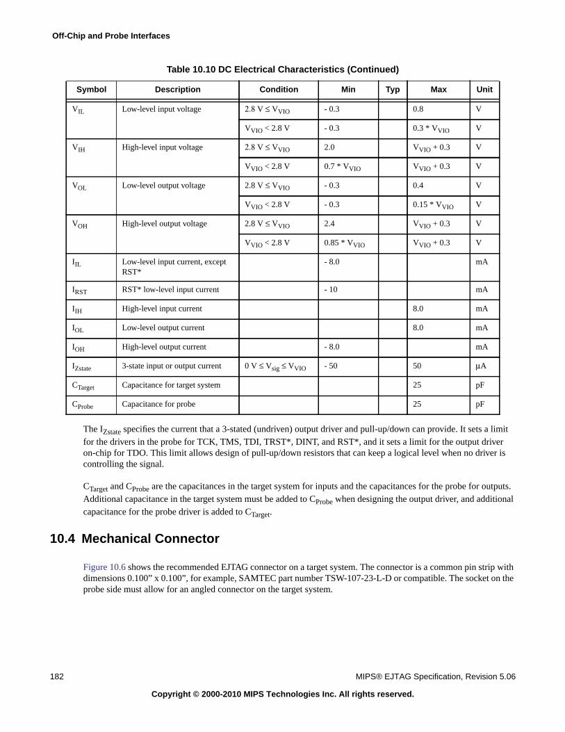
Off-Chip and Probe Interfaces
182 MIPS® EJTAG Specification, Revision 5.06
Copyright © 2000-2010 MIPS Technologies Inc. All rights reserved.
The IZstate specifies the current that a 3-stated (undriven) output driver and pull-up/down can provide. It sets a limitfor the drivers in the probe for TCK, TMS, TDI, TRST*, DINT, and RST*, and it sets a limit for the output driveron-chip for TDO. This limit allows design of pull-up/down resistors that can keep a logical level when no driver iscontrolling the signal.
CTarget and CProbe are the capacitances in the target system for inputs and the capacitances for the probe for outputs.Additional capacitance in the target system must be added to CProbe when designing the output driver, and additionalcapacitance for the probe driver is added to CTarget.
10.4 Mechanical Connector
Figure 10.6 shows the recommended EJTAG connector on a target system. The connector is a common pin strip withdimensions 0.100” x 0.100”, for example, SAMTEC part number TSW-107-23-L-D or compatible. The socket on theprobe side must allow for an angled connector on the target system.
VIL Low-level input voltage 2.8 V ≤ VVIO - 0.3 0.8 V
VVIO < 2.8 V - 0.3 0.3 * VVIO V
VIH High-level input voltage 2.8 V ≤ VVIO 2.0 VVIO + 0.3 V
VVIO < 2.8 V 0.7 * VVIO VVIO + 0.3 V
VOL Low-level output voltage 2.8 V ≤ VVIO - 0.3 0.4 V
VVIO < 2.8 V - 0.3 0.15 * VVIO V
VOH High-level output voltage 2.8 V ≤ VVIO 2.4 VVIO + 0.3 V
VVIO < 2.8 V 0.85 * VVIO VVIO + 0.3 V
IIL Low-level input current, exceptRST*
- 8.0 mA
IRST RST* low-level input current - 10 mA
IIH High-level input current 8.0 mA
IOL Low-level output current 8.0 mA
IOH High-level output current - 8.0 mA
IZstate 3-state input or output current 0 V ≤ Vsig ≤ VVIO - 50 50 µA
CTarget Capacitance for target system 25 pF
CProbe Capacitance for probe 25 pF
Table 10.10 DC Electrical Characteristics (Continued)
Symbol Description Condition Min Typ Max Unit
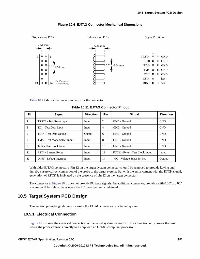
10.5 Target System PCB Design
MIPS® EJTAG Specification, Revision 5.06 183
Copyright © 2000-2010 MIPS Technologies Inc. All rights reserved.
Figure 10.6 EJTAG Connector Mechanical Dimensions
Table 10.11 shows the pin assignments for the connector.
With older EJTAG connectors, Pin 12 on the target system connector should be removed to provide keying andthereby ensure correct connection of the probe to the target system. But with the enhancement with the RTCK signal,generation of RTCK is indicated by the presence of pin 12 on the target connector.
The connector in Figure 10.6 does not provide PC trace signals. An additional connector, probably with 0.05” x 0.05”spacing, will be defined later when the PC trace feature is redefined.
10.5 Target System PCB Design
This section provides guidelines for using the EJTAG connector on a target system.
10.5.1 Electrical Connection
Figure 10.7 shows the electrical connection of the target system connector. This subsection only covers the casewhere the probe connects directly to a chip with an EJTAG compliant processor.
Table 10.11 EJTAG Connector Pinout
Pin Signal Direction Pin Signal Direction
1 TRST* - Test Reset Input Input 2 GND - Ground GND
3 TDI - Test Data Input Input 4 GND - Ground GND
5 TDO - Test Data Output Output 6 GND - Ground GND
7 TMS - Test Mode Select Input Input 8 GND - Ground GND
9 TCK - Test Clock Input Input 10 GND - Ground GND
11 RST* - System Reset Input 12 RTCK - Return Test Clock Input Input
13 DINT - Debug Interrupt Input 14 VIO - Voltage Sense for I/O Output
2.54 mm
Top view on PCB
2.54 mm
1 2
13 14Pin 12 removedto allow for key
0.64 mm
5.84 mm
Side view on PCB
GND
Signal Positions
1
GND
GND
GND
GND
key
VIO
TRST*
TDI
TDO
TMS
TCK
RST*
DINT
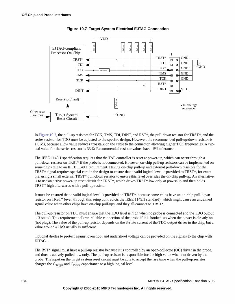
Off-Chip and Probe Interfaces
184 MIPS® EJTAG Specification, Revision 5.06
Copyright © 2000-2010 MIPS Technologies Inc. All rights reserved.
Figure 10.7 Target System Electrical EJTAG Connection
In Figure 10.7, the pull-up resistors for TCK, TMS, TDI, DINT, and RST*, the pull-down resistor for TRST*, and theseries resistor for TDO must be adjusted to the specific design. However, the recommended pull-up/down resistor is1.0 kΩ, because a low value reduces crosstalk on the cable to the connector, allowing higher TCK frequencies. Α typ-ical value for the series resistor is 33 Ω. Recommended resistor values have 5% tolerance.
The IEEE 1149.1 specification requires that the TAP controller is reset at power-up, which can occur through apull-down resistor on TRST* if the probe is not connected. However, on-chip pull-up resistors can be implemented onsome chips due to an IEEE 1149.1 requirement. Having on-chip pull-up and external pull-down resistors for theTRST* signal requires special care in the design to ensure that a valid logical level is provided to TRST*, for exam-ple, using a small external TRST* pull-down resistor to ensure this level overrides the on-chip pull-up. An alternativeis to use an active power-up reset circuit for TRST*, which drives TRST* low only at power-up and then holdsTRST* high afterwards with a pull-up resistor.
It must be ensured that a valid logical level is provided on TRST*, because some chips have an on-chip pull-downresistor on TRST* (even through this setup contradicts the IEEE 1149.1 standard), which might cause an undefinedsignal value when other chips have on-chip pull-ups, and they all connect to TRST*.
The pull-up resistor on TDO must ensure that the TDO level is high when no probe is connected and the TDO outputis 3-stated. This requirement allows reliable connection of the probe if it is hooked-up when the power is already on(hot plug). The value of the pull-up resistor depends on the 3-state current of the TDO output driver in the chip, but avalue around 47 kΩ usually is sufficient.
Optional diodes to protect against overshoot and undershoot voltage can be provided on the signals to the chip withEJTAG.
The RST* signal must have a pull-up resistor because it is controlled by an open-collector (OC) driver in the probe,and thus is actively pulled low only. The pull-up resistor is responsible for the high value when not driven by theprobe. The input on the target system reset circuit must be able to accept the rise time when the pull-up resistorcharges the CTarget and CProbe capacitance to a high logical level.
GND1
GND
GND
GND
GND
TRST*
TDI
TDO
TMS
TCK
RST*
DINT
TRST*
TDI
TDO
TMS
TCK
GND
DINT
VDD
GND
VIO voltagereference
Pull-
up
Pull-
up
Pull-
dow
n
Series-res.
Reset (soft/hard)
Target SystemReset Circuit
Pull-
up
Other resetsources
VIO
Pull-
up
Pull-
up
Pull-
up
EJTAG-compliantProcessor On Chip
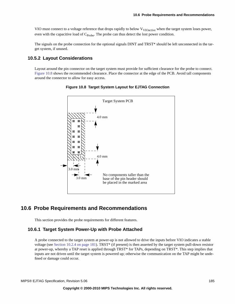
10.6 Probe Requirements and Recommendations
MIPS® EJTAG Specification, Revision 5.06 185
Copyright © 2000-2010 MIPS Technologies Inc. All rights reserved.
VIO must connect to a voltage reference that drops rapidly to below VVIOactive when the target system loses power,even with the capacitive load of CProbe. The probe can thus detect the lost power condition.
The signals on the probe connection for the optional signals DINT and TRST* should be left unconnected in the tar-get system, if unused.
10.5.2 Layout Considerations
Layout around the pin connector on the target system must provide for sufficient clearance for the probe to connect.Figure 10.8 shows the recommended clearance. Place the connector at the edge of the PCB. Avoid tall componentsaround the connector to allow for easy access.
Figure 10.8 Target System Layout for EJTAG Connection
10.6 Probe Requirements and Recommendations
This section provides the probe requirements for different features.
10.6.1 Target System Power-Up with Probe Attached
A probe connected to the target system at power-up is not allowed to drive the inputs before VIO indicates a stablevoltage (see Section 10.2.4 on page 181). TRST* (if present) is then asserted by the target system pull-down resistorat power-up, whereby a TAP reset is applied through TRST* for TAPs, depending on TRST*. This step implies thatinputs are not driven until the target system is powered up; otherwise the communication on the TAP might be unde-fined or damage could occur.
Target System PCB
4.0 mm
4.0 mm
3.0 mm
3.0 mmNo components taller than thebase of the pin header shouldbe placed in the marked area
1
Off-Chip and Probe Interfaces
186 MIPS® EJTAG Specification, Revision 5.06
Copyright © 2000-2010 MIPS Technologies Inc. All rights reserved.
At power-down the probe is not allowed to drive the inputs after VIO has dropped under a certain level (see Section10.2.4 on page 181).
The RST* signal is an exception to the above description because it can be driven low by the probe during power-up.
10.6.2 Hot Plug in of Probe
The probe must not drive any inputs to the target system if it is connected while the system is running (hot plug).Detection of a stable VIO from the target system is required before any input is allowed to be (see Section 10.2.4 onpage 181).
To avoid spikes or changes in the input voltage to the target system when the probe is connected, the level of the sig-nal on the probe must be adjusted to the same level as the signals on the target system. This adjustment can be donewith large pull-up/down resistors (in the range of 150 kΩ) on the probe signals, so the level of these signals matchesthe level on the target system shown in Figure 10.8. The specific implementation of this feature is dependent on theprobe, the driver type, etc. used in the probe.
10.6.3 TDO Level when 3-Stated
The probe must apply a pull-up resistor on TDO to have a well-defined logical level when TDO on the TAP is3-stated. The pull-up on the target system ensures the level at hot plug. The size of the pull-up on the probe isexpected to be 1.0 kΩ or more. The resistor value must be chosen so IZstate is observed.
10.6.4 RST* Drive by Open Collector
Drive the RST* signal with an open-collector (OC) output driver to allow for easy connection of the RST* signal inthe target system.
10.6.5 Changing TMS and TDI
It is recommended that the TMS and TDI signals driven by the probe change in relation to the falling edge generatedon the TCK, because this ensures a high setup and hold time for the TMS and TDI in relation to the rising edge ofTCK, on which these signals are sampled by the target processor.
If the TCK clock speed can be adjusted by extending the high and low period time of the TCK clock, then the behav-ior described above will also make the probe work even with a target processor not respecting setup and hold time,simply by lowering the TCK frequency.
10.6.6 Mechanical Connector
The female connector from the probe must allow for an angled board connector.
Block Hole 12 on the probe connector in order to provide keying and ensure correct connection of the probe to thetarget system. Connect the signal from the probe at line 12 to GND on the probe.
With the enhancement of the EJTAG connector with the input RTCK signal on pin 12, targets generating RTCK canonly be used with probes capable of accepting it. Generation of RTCK is indicated by the presence of pin 12 on thetarget connector. Probe acceptance of RTCK is indicated by lack of a plug on pin 12 of the probe cable.
Appendix A
MIPS® EJTAG Specification, Revision 5.06 187
Copyright © 2000-2010 MIPS Technologies Inc. All rights reserved.
Differences for R3000 Privileged Environments
This appendix describes the EJTAG feature differences necessary for integration with a 32-bit processor having anR3000 privileged environment.
A.1 EJTAG Processor Core Extensions
This section covers differences between an R3000 environment and the description in Chapter 2, “EJTAG ProcessorCore Extensions” on page 31.
A.1.1 SYNC Instruction
The SYNC instruction is not available for processors with R3000 privileged environment, but this instruction must beavailable and have behavior as described in Section 2.2.3.7 on page 38.
A.1.2 Debug Exception Vector Location
Table A.1 shows the debug exception vector location in system memory for processors with R3000 privileged envi-ronments.
The debug exception vector in dmseg (EJTAG memory) is the same for processors with R3000 and R4000 privilegedenvironments.
A.1.3 SYNC Instruction Substitute
In case the SYNC instruction is not provided (for example, on a processor with an R3000 privileged environment),then an implementation-specific instruction sequence must be used to ensure full update of the Debug register statusbits and BSn bits for hardware breakpoints with respect to handling of imprecise data hardware breakpoints andimprecise errors.
A.1.4 CP0 Register Numbers for Debug and DEPC Registers
The register numbers to use in processors with R3000 privileged environments for CP0 Debug and DEPC registers isshown below:
• Debug register: 16
• DEPC register: 17
Table A.1 Debug Exception Vector Location for R3k Privileged Environment Processors
ProbTrap bit inECR register Debug Exception Vector Address
0 0xBFC0 0200
Differences for R3000 Privileged Environments
188 MIPS® EJTAG Specification, Revision 5.06
Copyright © 2000-2010 MIPS Technologies Inc. All rights reserved.
A.2 Hardware Breakpoints
This section describes the differences between hardware breakpoints in an R3000 privileged environment and thosedescribes in Chapter 5, “Hardware Breakpoints” on page 111.
A.2.1 Instruction Breakpoint Registers
Table A.2 shows the address offsets in drseg for the Instruction Breakpoint registers. In the table, n is the breakpointnumber in the range 0 to 14.
A.2.2 Conditions for Matching Instruction Breakpoints
The width in bits of the ASID field for the compare is 6 bits, as is the size used in the TLB. The ASID andIBASIDnASID references used in the equations in Section 5.3.1 on page 114 has this size.
A.2.3 ASID Field in IBCn Register
Compliance Level: Required with instruction breakpoints when the ASIDsup bit in the IBS register is 1, optionalotherwise.
The ASID field has the ASID value used in the compare for instruction breakpoint n; it is placed in the IBCn register,not in a register of its own. Table A.3 shows the format of the ASID field.
A.2.4 Data Breakpoint Registers
Table A.4 shows the address offsets in drseg for the Data Breakpoint registers. In the table, n is the breakpoint num-ber in the range 0 to 14.
Table A.2 Offsets for Instruction Breakpoint Registers for R3k Privileged Environment Processors
Offset in drsegRegister
Mnemonic Register Name and Description
0x0004 IBS Instruction Breakpoint Status
0x0100 + 0x010 * n IBAn Instruction Breakpoint Address n
0x0104 + 0x010 * n IBCn Instruction Breakpoint Control and ASID n
0x0108 + 0x010 * n IBMn Instruction Breakpoint Address Mask n
Table A.3 ASID Field in IBCn Register
Fields
DescriptionRead/Write Reset StateName Bits
ASID 29:24 Instruction breakpoint ASID value for compare. R/W Undefined
Table A.4 Offsets for Data Breakpoint Registers for R3k Privileged Environment Processors
Offset in drsegRegister
Mnemonic Register Name and Description
0x0008 DBS Data Breakpoint Status
A.3 EJTAG Test Access Port
MIPS® EJTAG Specification, Revision 5.06 189
Copyright © 2000-2010 MIPS Technologies Inc. All rights reserved.
A.2.5 Conditions for Matching Data Breakpoints
The width in bits of the ASID field for the compare is 6 bits, as is the size used in the TLB. The ASID andDBASIDnASID references used in the equations in Section 5.3.2 on page 116 has this size.
A.2.6 ASID Field in DBCn Register
Compliance Level: Required with instruction breakpoints when the ASIDsup bit in the DBS register is 1, optionalotherwise.
The ASID field has the ASID value used in the compare for data breakpoint n; it is placed in the DBCn register, notin a register of its own. Table A.5 shows the format of the ASID field.
A.3 EJTAG Test Access Port
There are no differences for processors with R3000 privileged environment with respect to the EJTAG Test AccessPort. The R4000/R3000 bit in the Implementation register selects between R4000 and R3000 privileged environ-ments (see Section 4.5.2 on page 90).
0x0200 + 0x010 * n DBAn Data Breakpoint Address n
0x0204 + 0x010 * n DBCn Data Breakpoint Control and ASID n
0x0208 + 0x010 * n DBMn Data Breakpoint Address Mask n
0x020C + 0x010 * n DBVn Data Breakpoint Value n
Table A.5 ASID Field in DBCn Register
Fields
DescriptionRead/Write Reset StateName Bits
ASID 29:24 Data breakpoint ASID value for compare. R/W Undefined
Table A.4 Offsets for Data Breakpoint Registers for R3k Privileged Environment Processors (Continued)
Offset in drsegRegister
Mnemonic Register Name and Description
Differences for R3000 Privileged Environments
190 MIPS® EJTAG Specification, Revision 5.06
Copyright © 2000-2010 MIPS Technologies Inc. All rights reserved.
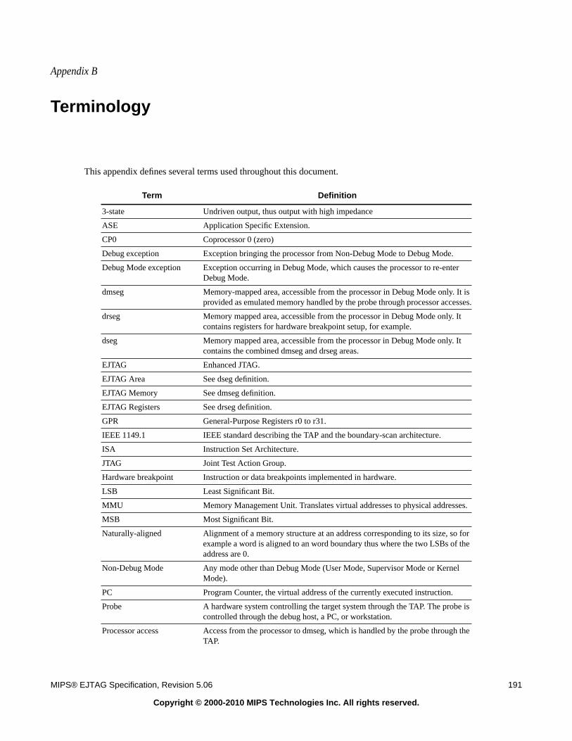
Appendix B
MIPS® EJTAG Specification, Revision 5.06 191
Copyright © 2000-2010 MIPS Technologies Inc. All rights reserved.
Terminology
This appendix defines several terms used throughout this document.
Term Definition
3-state Undriven output, thus output with high impedance
ASE Application Specific Extension.
CP0 Coprocessor 0 (zero)
Debug exception Exception bringing the processor from Non-Debug Mode to Debug Mode.
Debug Mode exception Exception occurring in Debug Mode, which causes the processor to re-enterDebug Mode.
dmseg Memory-mapped area, accessible from the processor in Debug Mode only. It isprovided as emulated memory handled by the probe through processor accesses.
drseg Memory mapped area, accessible from the processor in Debug Mode only. Itcontains registers for hardware breakpoint setup, for example.
dseg Memory mapped area, accessible from the processor in Debug Mode only. Itcontains the combined dmseg and drseg areas.
EJTAG Enhanced JTAG.
EJTAG Area See dseg definition.
EJTAG Memory See dmseg definition.
EJTAG Registers See drseg definition.
GPR General-Purpose Registers r0 to r31.
IEEE 1149.1 IEEE standard describing the TAP and the boundary-scan architecture.
ISA Instruction Set Architecture.
JTAG Joint Test Action Group.
Hardware breakpoint Instruction or data breakpoints implemented in hardware.
LSB Least Significant Bit.
MMU Memory Management Unit. Translates virtual addresses to physical addresses.
MSB Most Significant Bit.
Naturally-aligned Alignment of a memory structure at an address corresponding to its size, so forexample a word is aligned to an word boundary thus where the two LSBs of theaddress are 0.
Non-Debug Mode Any mode other than Debug Mode (User Mode, Supervisor Mode or KernelMode).
PC Program Counter, the virtual address of the currently executed instruction.
Probe A hardware system controlling the target system through the TAP. The probe iscontrolled through the debug host, a PC, or workstation.
Processor access Access from the processor to dmseg, which is handled by the probe through theTAP.
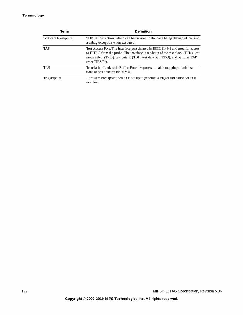
Terminology
192 MIPS® EJTAG Specification, Revision 5.06
Copyright © 2000-2010 MIPS Technologies Inc. All rights reserved.
Software breakpoint SDBBP instruction, which can be inserted in the code being debugged, causinga debug exception when executed.
TAP Test Access Port. The interface port defined in IEEE 1149.1 and used for accessto EJTAG from the probe. The interface is made up of the test clock (TCK), testmode select (TMS), test data in (TDI), test data out (TDO), and optional TAPreset (TRST*).
TLB Translation Lookaside Buffer. Provides programmable mapping of addresstranslations done by the MMU.
Triggerpoint Hardware breakpoint, which is set up to generate a trigger indication when itmatches.
Term Definition
Appendix C
MIPS® EJTAG Specification, Revision 5.06 193
Copyright © 2000-2010 MIPS Technologies Inc. All rights reserved.
Functional Clarifications from Old EJTAG 2.5
The following items were clarified from the previous EJTAG rev. 2.5 Specification:
• Update of Instruction register in Update-IR state
Updating Instruction register in the Update-IR state is allowed either on the rising or the falling TCK edge. SeeSection 4.3.4 on page 85 for more information.
• Update of selected Data register(s) in Update-DR state
Updating selected Data register(s) in the Update-IR state is allowed either on the rising or the falling TCK edge.See Section 4.3.7 on page 85 for more information.
• Use of the Device ID register
The Device ID register is recommended to be unique among designs and among several processors on the samechip. See Section 4.5.1 on page 89 for more information.
• Reset State or Power-up State
Either the reset state or the power-up state is indicated for the data registers. It is not possible to state only thereset value, because a reset denotes a processor reset. For example, the Bypass register must be reset to 1 as soonas the TAP can be operated, thus the processor should not be required to be reset first. See Section 4.5 on page 88for more information.
• SRstE Changed to Optional
The SRstE bit described in Chapter 3, “Debug Control Register” on page 75 has been made optional, because notevery implementation needs it, and its behavior is defined as implementation-dependent.
• Bypass Register Initial Value as 0 (zero)
The initial value for the Bypass register (in Capture-DR state) is defined as 0 (see Section 4.5.8 on page 105),since the JTAG Specification requires this in chapter 9 page 9-1.
Functional Clarifications from Old EJTAG 2.5
194 MIPS® EJTAG Specification, Revision 5.06
Copyright © 2000-2010 MIPS Technologies Inc. All rights reserved.
Appendix D
MIPS® EJTAG Specification, Revision 5.06 195
Copyright © 2000-2010 MIPS Technologies Inc. All rights reserved.
Multithreaded and Multi-Core Debug
Multicore debugging is not a required feature of EJTAG, but is provided here as a recommended method to imple-ment debug for a multi-core or a multithreaded processor.
D.1 Introduction
This document serves as a guideline for designing a Multi-Core Breakpoint Unit (MCBU) for System-On-Chip(SOC) devices that integrate multiple MIPS processor cores. The document is intended to be used by designers ofSOC devices and by software tool vendors who design debuggers capable of interacting with these SOC devices.
The MCBU is capable of requesting a debug interrupt from any number of cores in the SOC as a result of any core inthe system entering Debug Mode. In addition, the MCBU can be used to request a debug interrupt, soft reset, hardreset, and non-maskable interrupt from any number of the cores under software control.
D.2 MCBU Register Map
The MCBU consists of registers that specify which of the processors in the multi-processor system should receive aRESET, COLD RESET, NMI, and Debug Interrupt signal. There are also per-processor debug interrupt registers thatspecify whether that processor causes a debug interrupt to be sent to other processors in the multi-processor system.These registers are described below. These registers are memory-mapped for access by the debug probe hardware andsoftware. Refer to Table D.1 and Table D.2.
Table D.1 sMCBU Register Memory Map
Register Name Memory Map of the Register
Reset Base+0x000
Cold_Reset Base+0x010
NMI Base+0x020
Debug_Interrupt Base+0x030
Table D.2 MCBU Debug_Int Register Memory Map
Register Name Memory Map of the Register
Debug_Int_0 Base+0x200
Debug_Int_1 Base+0x210
Debug_Int_2 Base+0x220
... ...
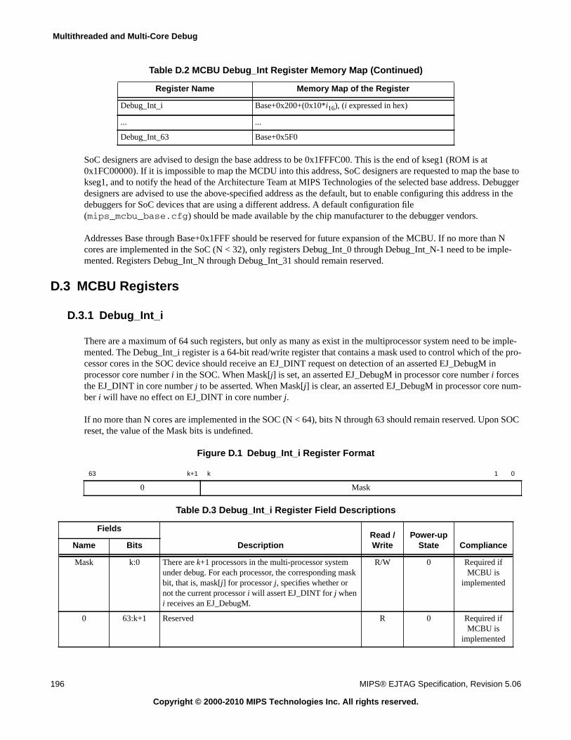
Multithreaded and Multi-Core Debug
196 MIPS® EJTAG Specification, Revision 5.06
Copyright © 2000-2010 MIPS Technologies Inc. All rights reserved.
SoC designers are advised to design the base address to be 0x1FFFC00. This is the end of kseg1 (ROM is at0x1FC00000). If it is impossible to map the MCDU into this address, SoC designers are requested to map the base tokseg1, and to notify the head of the Architecture Team at MIPS Technologies of the selected base address. Debuggerdesigners are advised to use the above-specified address as the default, but to enable configuring this address in thedebuggers for SoC devices that are using a different address. A default configuration file(mips_mcbu_base.cfg) should be made available by the chip manufacturer to the debugger vendors.
Addresses Base through Base+0x1FFF should be reserved for future expansion of the MCBU. If no more than Ncores are implemented in the SoC (N < 32), only registers Debug_Int_0 through Debug_Int_N-1 need to be imple-mented. Registers Debug_Int_N through Debug_Int_31 should remain reserved.
D.3 MCBU Registers
D.3.1 Debug_Int_i
There are a maximum of 64 such registers, but only as many as exist in the multiprocessor system need to be imple-mented. The Debug_Int_i register is a 64-bit read/write register that contains a mask used to control which of the pro-cessor cores in the SOC device should receive an EJ_DINT request on detection of an asserted EJ_DebugM inprocessor core number i in the SOC. When Mask[j] is set, an asserted EJ_DebugM in processor core number i forcesthe EJ_DINT in core number j to be asserted. When Mask[j] is clear, an asserted EJ_DebugM in processor core num-ber i will have no effect on EJ_DINT in core number j.
If no more than N cores are implemented in the SOC (N < 64), bits N through 63 should remain reserved. Upon SOCreset, the value of the Mask bits is undefined.
Figure D.1 Debug_Int_i Register Format
Debug_Int_i Base+0x200+(0x10*i16), (i expressed in hex)
... ...
Debug_Int_63 Base+0x5F0
63 k+1 k 1 0
0 Mask
Table D.3 Debug_Int_i Register Field Descriptions
Fields
DescriptionRead /Write
Power-upState ComplianceName Bits
Mask k:0 There are k+1 processors in the multi-processor systemunder debug. For each processor, the corresponding maskbit, that is, mask[j] for processor j, specifies whether ornot the current processor i will assert EJ_DINT for j wheni receives an EJ_DebugM.
R/W 0 Required ifMCBU is
implemented
0 63:k+1 Reserved R 0 Required ifMCBU is
implemented
Table D.2 MCBU Debug_Int Register Memory Map (Continued)
Register Name Memory Map of the Register
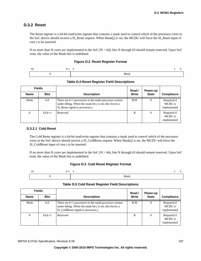
D.3 MCBU Registers
MIPS® EJTAG Specification, Revision 5.06 197
Copyright © 2000-2010 MIPS Technologies Inc. All rights reserved.
D.3.2 Reset
The Reset register is a 64-bit read/write register that contains a mask used to control which of the processor cores inthe SoC device should receive a SI_Reset request. When Mask[j] is set, the MCDU will force the SI_Reset input ofcore j to be asserted.
If no more than N cores are implemented in the SoC (N < 64), bits N through 63 should remain reserved. Upon SoCreset, the value of the Mask bits is undefined.
Figure D.2 Reset Register Format
D.3.2.1 Cold Reset
The Cold Reset register is a 64-bit read/write register that contains a mask used to control which of the processorcores in the SoC device should receive a SI_ColdReset request. When Mask[j] is set, the MCDU will force theSI_ColdReset input of core j to be asserted.
If no more than N cores are implemented in the SoC (N < 64), bits N through 63 should remain reserved. Upon SoCreset, the value of the Mask bits is undefined.
Figure D.3 Cold Reset Register Format
63 k+1 k 1 0
0 Mask
Table D.4 Reset Register Field Descriptions
Fields
DescriptionRead /Write
Power-upState ComplianceName Bits
Mask k:0 There are k+1 processors in the multi-processor systemunder debug. When the mask bit j is set, this forces aSI_Reset signal to processor j.
R/W 0 Required ifMCBU is
implemented
0 63:k+1 Reserved R 0 Required ifMCBU is
implemented
63 k+1 k 1 0
0 Mask
Table D.5 Cold Reset Register Field Descriptions
Fields
DescriptionRead /Write
Power-upState ComplianceName Bits
Mask k:0 There are k+1 processors in the multi-processor systemunder debug. When the mask bit j is set, this forces aSI_ColdReset signal to processor j.
R/W 0 Required ifMCBU is
implemented
0 63:k+1 Reserved R 0 Required ifMCBU is
implemented
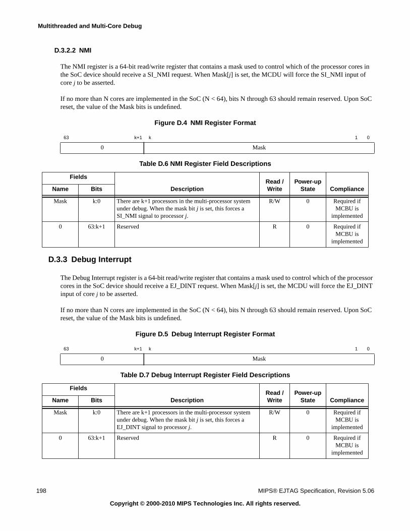
Multithreaded and Multi-Core Debug
198 MIPS® EJTAG Specification, Revision 5.06
Copyright © 2000-2010 MIPS Technologies Inc. All rights reserved.
D.3.2.2 NMI
The NMI register is a 64-bit read/write register that contains a mask used to control which of the processor cores inthe SoC device should receive a SI_NMI request. When Mask[j] is set, the MCDU will force the SI_NMI input ofcore j to be asserted.
If no more than N cores are implemented in the SoC (N < 64), bits N through 63 should remain reserved. Upon SoCreset, the value of the Mask bits is undefined.
Figure D.4 NMI Register Format
D.3.3 Debug Interrupt
The Debug Interrupt register is a 64-bit read/write register that contains a mask used to control which of the processorcores in the SoC device should receive a EJ_DINT request. When Mask[j] is set, the MCDU will force the EJ_DINTinput of core j to be asserted.
If no more than N cores are implemented in the SoC (N < 64), bits N through 63 should remain reserved. Upon SoCreset, the value of the Mask bits is undefined.
Figure D.5 Debug Interrupt Register Format
63 k+1 k 1 0
0 Mask
Table D.6 NMI Register Field Descriptions
Fields
DescriptionRead /Write
Power-upState ComplianceName Bits
Mask k:0 There are k+1 processors in the multi-processor systemunder debug. When the mask bit j is set, this forces aSI_NMI signal to processor j.
R/W 0 Required ifMCBU is
implemented
0 63:k+1 Reserved R 0 Required ifMCBU is
implemented
63 k+1 k 1 0
0 Mask
Table D.7 Debug Interrupt Register Field Descriptions
Fields
DescriptionRead /Write
Power-upState ComplianceName Bits
Mask k:0 There are k+1 processors in the multi-processor systemunder debug. When the mask bit j is set, this forces aEJ_DINT signal to processor j.
R/W 0 Required ifMCBU is
implemented
0 63:k+1 Reserved R 0 Required ifMCBU is
implemented
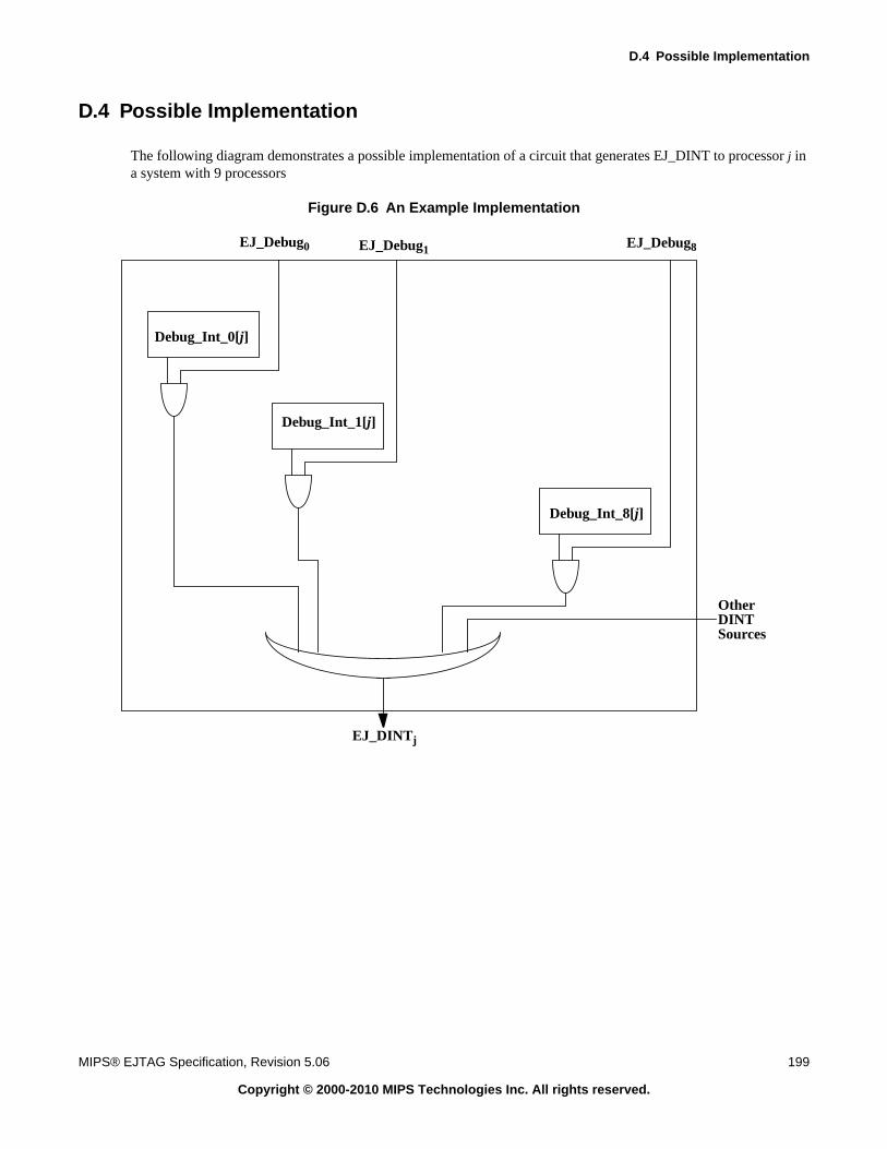
D.4 Possible Implementation
MIPS® EJTAG Specification, Revision 5.06 199
Copyright © 2000-2010 MIPS Technologies Inc. All rights reserved.
D.4 Possible Implementation
The following diagram demonstrates a possible implementation of a circuit that generates EJ_DINT to processor j ina system with 9 processors
Figure D.6 An Example Implementation
Debug_Int_0[j]
Debug_Int_1[j]
Debug_Int_8[j]
EJ_Debug0 EJ_Debug1 EJ_Debug8
OtherDINTSources
EJ_DINTj
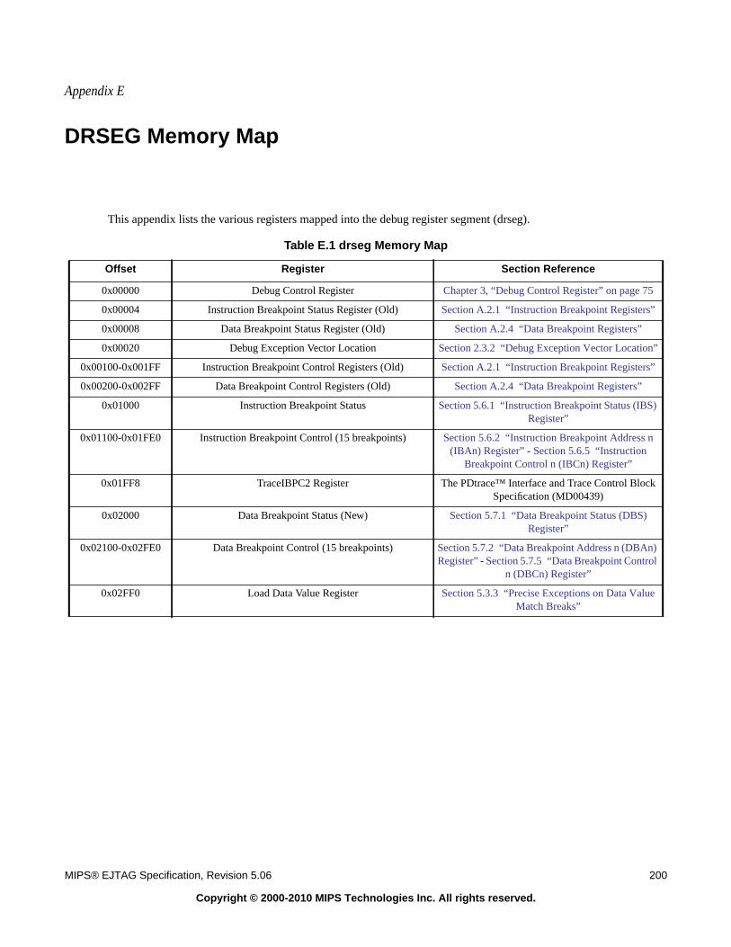
Appendix E
MIPS® EJTAG Specification, Revision 5.06 200
Copyright © 2000-2010 MIPS Technologies Inc. All rights reserved.
DRSEG Memory Map
This appendix lists the various registers mapped into the debug register segment (drseg).
Table E.1 drseg Memory Map
Offset Register Section Reference
0x00000 Debug Control Register Chapter 3, “Debug Control Register” on page 75
0x00004 Instruction Breakpoint Status Register (Old) Section A.2.1 “Instruction Breakpoint Registers”
0x00008 Data Breakpoint Status Register (Old) Section A.2.4 “Data Breakpoint Registers”
0x00020 Debug Exception Vector Location Section 2.3.2 “Debug Exception Vector Location”
0x00100-0x001FF Instruction Breakpoint Control Registers (Old) Section A.2.1 “Instruction Breakpoint Registers”
0x00200-0x002FF Data Breakpoint Control Registers (Old) Section A.2.4 “Data Breakpoint Registers”
0x01000 Instruction Breakpoint Status Section 5.6.1 “Instruction Breakpoint Status (IBS)Register”
0x01100-0x01FE0 Instruction Breakpoint Control (15 breakpoints) Section 5.6.2 “Instruction Breakpoint Address n(IBAn) Register” - Section 5.6.5 “Instruction
Breakpoint Control n (IBCn) Register”
0x01FF8 TraceIBPC2 Register The PDtrace™ Interface and Trace Control BlockSpecification (MD00439)
0x02000 Data Breakpoint Status (New) Section 5.7.1 “Data Breakpoint Status (DBS)Register”
0x02100-0x02FE0 Data Breakpoint Control (15 breakpoints) Section 5.7.2 “Data Breakpoint Address n (DBAn)Register” - Section 5.7.5 “Data Breakpoint Control
n (DBCn) Register”
0x02FF0 Load Data Value Register Section 5.3.3 “Precise Exceptions on Data ValueMatch Breaks”
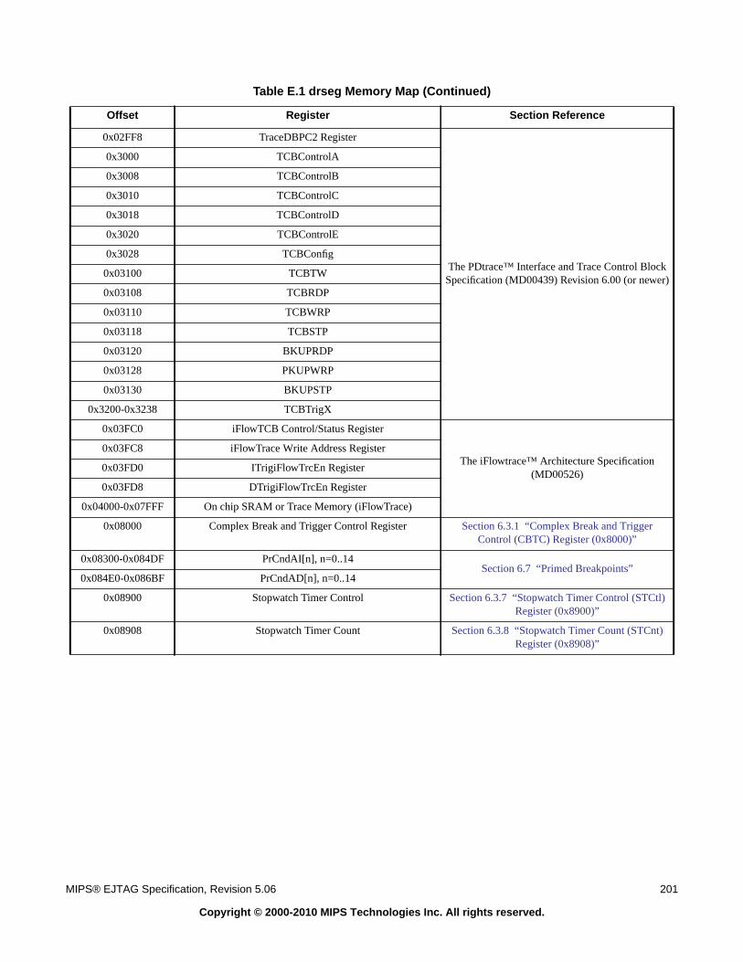
MIPS® EJTAG Specification, Revision 5.06 201
Copyright © 2000-2010 MIPS Technologies Inc. All rights reserved.
0x02FF8 TraceDBPC2 Register
The PDtrace™ Interface and Trace Control BlockSpecification (MD00439) Revision 6.00 (or newer)
0x3000 TCBControlA
0x3008 TCBControlB
0x3010 TCBControlC
0x3018 TCBControlD
0x3020 TCBControlE
0x3028 TCBConfig
0x03100 TCBTW
0x03108 TCBRDP
0x03110 TCBWRP
0x03118 TCBSTP
0x03120 BKUPRDP
0x03128 PKUPWRP
0x03130 BKUPSTP
0x3200-0x3238 TCBTrigX
0x03FC0 iFlowTCB Control/Status Register
The iFlowtrace™ Architecture Specification(MD00526)
0x03FC8 iFlowTrace Write Address Register
0x03FD0 ITrigiFlowTrcEn Register
0x03FD8 DTrigiFlowTrcEn Register
0x04000-0x07FFF On chip SRAM or Trace Memory (iFlowTrace)
0x08000 Complex Break and Trigger Control Register Section 6.3.1 “Complex Break and TriggerControl (CBTC) Register (0x8000)”
0x08300-0x084DF PrCndAI[n], n=0..14Section 6.7 “Primed Breakpoints”
0x084E0-0x086BF PrCndAD[n], n=0..14
0x08900 Stopwatch Timer Control Section 6.3.7 “Stopwatch Timer Control (STCtl)Register (0x8900)”
0x08908 Stopwatch Timer Count Section 6.3.8 “Stopwatch Timer Count (STCnt)Register (0x8908)”
Table E.1 drseg Memory Map (Continued)
Offset Register Section Reference
DRSEG Memory Map
202 MIPS® EJTAG Specification, Revision 5.06
Copyright © 2000-2010 MIPS Technologies Inc. All rights reserved.
Appendix F
MIPS® EJTAG Specification, Revision 5.06 203
Copyright © 2000-2010 MIPS Technologies Inc. All rights reserved.
Revision History
MIPS documents include change bars (vertical bars in the page margin) that mark significant changes to the docu-ment since its last release. Change bars are removed for changes which are more than one revision old.
This document may refer to Architecture specifications (for example, instruction set descriptions and EJTAG registerdefinitions), and change bars in these sections indicate changes since the previous version of the relevant Architecturedocument.
Revision Date Description
2.5 February 22, 2000 Release to users under NDA
2.5-1 June 6, 2000 Changes in this revision:• Clarification describing possible speculative fetch from dmseg. See Section
2.2.2.1 on page 35.• Clarification of SYNC instruction behavior in Section 2.2.3.7 on page 38.• Added hazard description on DEBUG[LSNM] and DEBUG[IEXI] in Section
2.2.4 on page 39.• Clarification for Doze and Halt bits in Debug register, see Section 2.7.1 on
page 56.• Removed requirement that bytes of TAP Data Register which are not accessed
for a processor access read must be written with 0s by the probe. Thus, nowany value may be written to the not accessed bytes.
• Wording change in headline and beginning of Appendix C covering clarifica-tion of changes since previous EJTAG revisions.
• Added cross references for clarification.• Corrected typos.• Declassify the document.
2.5-2 August 22, 2000 Removed old Section 6.2, and added Section 6.4 to discuss multi-core EJTAG,i.e., MIPS recommended way to connect multiple TAP controllers to one set ofexternal EJTAG TAP pins.
02.53 January 8, 2001 Changes in this revision:• Revision number changed to have format XX.YY, thus the next minor revision
after 2.5-2 is named 02.53.• Clarification of data triggerpoint handling when exception occur on a
load/store instruction.• Clarification of value of BYTELANE for hardware breakpoints when access
with unaligned address occurs.• Elaborated description of fields in TAP Device ID register.• Added recommendation for handling of CacheErr register in Debug Mode.• Modified description of connecting multiple TAP controllers in daisy chain.• Updates for clarifications in general.• Corrected typos.
Revision History
204 MIPS® EJTAG Specification, Revision 5.06
Copyright © 2000-2010 MIPS Technologies Inc. All rights reserved.
02.60 February 15, 2001 Changes in this revision:• Updated the chapter on TAP controller to specify the FASTDATA instruction.• Added the instructions needed for the trace control block register access.• Updated the revision number to 02.60 and made a value of 2 in the EJTAGver
field correspond to this version.
02.61 September 30, 2002 Changes in this revision:• Include the EJTAGver field encoding of 2, inadvertently left out of version
2.60.
02.62 May 7, 2003 Changes in this revision:• Remove Appendix D, as this information in not appropriate to a specification
documenting the current state of the EJTAG architecture.• Clarify the definition of EJTAGBOOT. If this condition is active, the first
instruction fetch after reset is to one of the EJTAG debug addresses, not to thereset exception vector.
• Clarify the wording describing the BAI field of the Data Breakpoint Controlregister.
• Clarify the definition of ADDR for the LUXC1 and SUXC1 instructions,when used in the data breakpoint address match equation.
• Clarify the use of the DebugDExcCode field for SDBBP instructions in Debug
Mode.• Add an introduction to EJTAG to the first chapter of the specification.• Clarify the state of the Halt and Doze bits in the Debug register if a hardware
interrupt or other event awakens the processor, but a debug exception is takeninstead.
• Make it clear that it is implementation-dependent whether an SC/SCD, whichwould fail because the LLbit is 0, will cause a debug exception due to a databreakpoint match.
• Update with MIPS32 and MIPS64 Release 2 Architecture changes.
3.10 July 5, 2005 Changes in this revision:• Added PC Sampling feature• Added support for MIPS MT ASE• EJTAG version 3 for specification revision 3.10 and up• Inclusion of a possible proposal for implementing EJTAG support for multiple
processors or a multi-threaded configuration• Miscellaneous cleanup
3.20 September 19, 2005 Changes in this revision:• PC sampling clarifications for MT, add a PCSe bit to DCR• Typo fixes
4.00 June 28, 2006 Changes in this revision:• Add complex break and trigger chapter and the Debug2 register• Add the ability to Invert a data value check• Add the feature that saves a data value on a precise match• Typo fixes and clarification.
4.10 July 3, 2006 Fix typographical errors, unresolved pointers, and clarification of existing fea-tures. Add a new Return TCk (RTCK) signal to pin 12 of the EJTAG Connector.
4.11 May 18, 2007 Add EJTAGJver 4.0 to indicate the architecture upgrade to include the ComplexBreak and Trigger feature.
4.12 July 15, 2008 Update copyrights and contact information.
Revision Date Description
MIPS® EJTAG Specification, Revision 5.06 205
Copyright © 2000-2010 MIPS Technologies Inc. All rights reserved.
4.13 August 01, 2008 • DBCCn Register figure was missing UnPRCnd field.• Load Data Value address offset is 0x2FF0.• Page 16, Table 1.1 and Page 138, 7.5.5.1 gave the wrong impression that
EJTAGBOOT and NORMALBoot commands cause reset themselves.
4.14 November 06, 2008 • Added new TAP instructions• Added drseg map appendix
4.5 January 26, 2009 MIPS Technologies-only release for internal review:• Added Fast Debug Channel control bits to DCR• Added Fast Debug Channel Chapter• Added information about relocatable debug vector• Added Data Address Sampling and enhanced PC Sampling.• Added TIBrkNum and TUP fields to DBCCn register description• Moved UnPrCnd field in DBCCn registers to avoid overlap with above fields• Added UnPrCnd field to IBCCn register
4.51 April 8, 2009 MIPS Technologies-only release for internal review:• Changes to ISAOnDebug bit for reset state and microMIPS-only case.
4.52 April 20, 2009 MIPS Technologies-only release for internal review:• Added MIPS64 definition for PCSAMPLE TAP register• Updated sections relating to debug vector relocation• Updated sections relating to ISA mode selection for debug exception handlers• Clarified that FDC is optional, fixed typos in FDC chapter• Updated list of memory mapped registers in Introduction and Appendix• Added new version number for 4.5• Clarified that PC sampling is available from version 3 onwards• Updated description of DEPC to include ISA mode bit
4.53 Aptil 24, 2009 MIPS Technologies-only release for internal review:• microMIPS edits.
5.00 July 20, 2009 External release of all new features post revision 4.14:• Corrected bitfield descriptions for DBASIDn.VPE, DBCn.VPEuse• Changed DCR bit RDVec - now optional• Changed DCR bits PCIM, PCnoASID, PCR - write optional• Changed DebugVectorAddr - now optional, bit 7 is r/w• Added DCR bit PCnoTCID
5.01 October 05,2009 • IMPCODE.EJTAGVer field - added missing identifier for revision 5.00.• Additional text for DebugVectorAddr register - how vector is actually calcu-
lated for different exceptions. Some clean-up for that description.
5.02 November 16,2009 • Many of the embedded tables (tables within tables) in Chapter 8 were clippedoff at the bottom so you couldn’t see the last entry. These have been fixed.
• ISAMode bit only exists if microMIPS ISA is implemented.
5.03 November 18,2009 • Moved Core Extensions, DCR and TAP chapters ahead of chapters describingoptional features.
• Renamed a few chapters.
5.04 March 01, 2010 • Remove “Preliminary” Margin Note.
5.05 November 25, 2010 • Clarify EJTAGboot behavior - only affects instruction fetch, not exceptiontype.
5.06 March 05,2011 • Added CPUNum & Type field to IMPCODE register.
Revision Date Description