Embed Size (px)
Citation preview
f. m. rotella FILENAME: oralspres2.fmk DATE: June 4, 1998 2:49 pmPAGE: 1
Mixed Circuit and Device Simulation forModeling, Analyzing, and
Designing RF Devices
Francis Rotella
Integrated Circuits LabStanford University
June 5, 1998
Center for Integrated Systems 2 of 39 June 5, 1998
Motivation: Wireless Growth
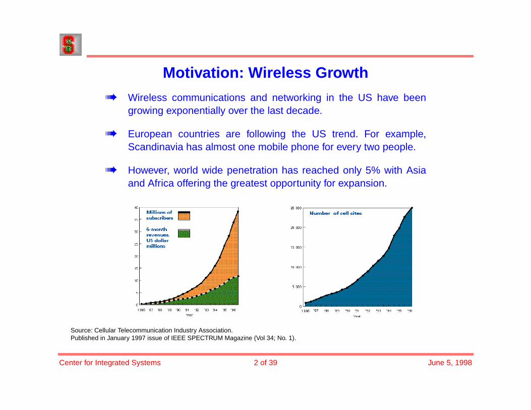
Wireless communications and networking in the US have beengrowing exponentially over the last decade.
European countries are following the US trend. For example,Scandinavia has almost one mobile phone for every two people.
However, world wide penetration has reached only 5% with Asiaand Africa offering the greatest opportunity for expansion.
Source: Cellular Telecommunication Industry Association.Published in January 1997 issue of IEEE SPECTRUM Magazine (Vol 34; No. 1).
Center for Integrated Systems 3 of 39 June 5, 1998
Motivation: TCAD Tools are Critical
In order to meet the demands of these expanding markets, nextgeneration semiconductor technology (chip level and discrete RFpower devices) need to be developed quickly, produced in highvolume, and sold at low cost.
Over the last decades, to meet the challenges of new technologydevelopment TCAD tools such as PISCES (aka Medici from Avant!and Atlas from Silvaco) played a critical role in understandingdevice design and performance trade-off.
Recent work and this talk examines the role of PISCES in RFdevice design in order to meet the challenges of the growingmarkets in wireless communications.
a. Development of the harmonic balance solver for the deviceequations. (Boris Troyanovsky)
b. Inclusion of circuit components in the device simulation andharmonic balance simulation.
c. Accurate modeling techniques to develop an RF representation ofa device.
Center for Integrated Systems 4 of 39 June 5, 1998
Outline of Talk
Tools: Coupling Circuit and Device Simulation
a. Full-Newton Algorithm
b. Two-Level Newton Algorithm
c. Reduction to Boundary Condition Equations
Tools: Harmonic Balance Simulation
a. Harmonic Balance Simulation
b. Boundary Conditions for HB Simulation
Example: Modeling RF LDMOS Discrete Transistors
a. Device Structure and Operation
b. Model for the Device
c. Model Verification
Example: Analysis and Design of LDMOS Discrete Transistors
a. Gain, Efficiency, and Inter-modulation Distortion
b. Variation in Parasitic Components
c. Matching Network Effects
Center for Integrated Systems 5 of 39 June 5, 1998
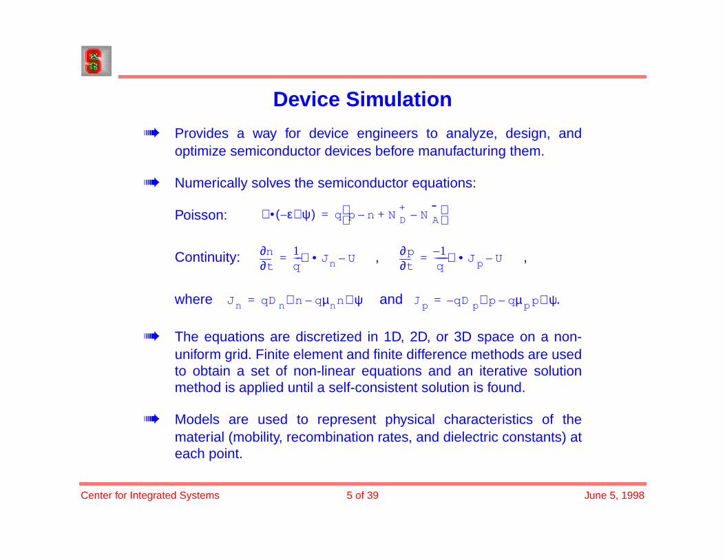
Device Simulation
Provides a way for device engineers to analyze, design, andoptimize semiconductor devices before manufacturing them.
Numerically solves the semiconductor equations:
Poisson:
Continuity: , ,
where and .
The equations are discretized in 1D, 2D, or 3D space on a non-uniform grid. Finite element and finite difference methods are usedto obtain a set of non-linear equations and an iterative solutionmethod is applied until a self-consistent solution is found.
Models are used to represent physical characteristics of thematerial (mobility, recombination rates, and dielectric constants) ateach point.
ε ψ∇–( )∇• q p n– N D+
N A-
–+ =
t∂∂n 1
q---∇ Jn U–•=
t∂∂p 1–
q------∇ J p U–•=
Jn qD n∇ n qµnn∇ψ–= J p q– D p∇ p qµpp∇ ψ–=
Center for Integrated Systems 6 of 39 June 5, 1998
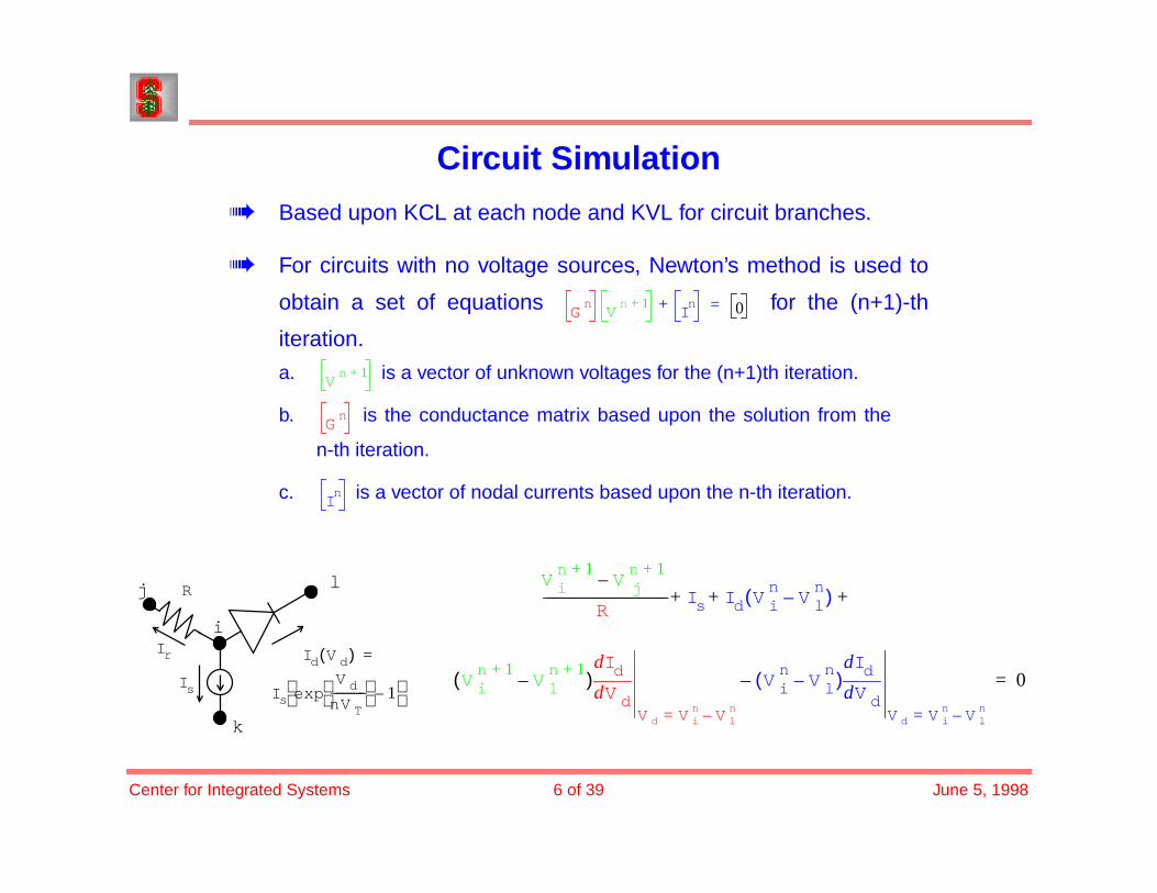
Circuit Simulation
Based upon KCL at each node and KVL for circuit branches.
For circuits with no voltage sources, Newton’s method is used to
obtain a set of equations for the (n+1)-th
iteration.
a. is a vector of unknown voltages for the (n+1)th iteration.
b. is the conductance matrix based upon the solution from the
n-th iteration.
c. is a vector of nodal currents based upon the n-th iteration.
Id V d( ) =
Is
Ir
R l
i
j
k
V in 1+
V jn 1+
–
R-------------------------------------- Is Id V i
nV ln
–( )+ + +
IsV d
nV T------------
exp 1– V i
n 1+V ln 1+
–( )V dd
dId
V d V in
V ln–=
V in
V ln
–( )–V dd
dId
V d V in
V ln–=
0=
Gn
Vn 1+
In+ 0=
Vn 1+
Gn
In
Center for Integrated Systems 7 of 39 June 5, 1998
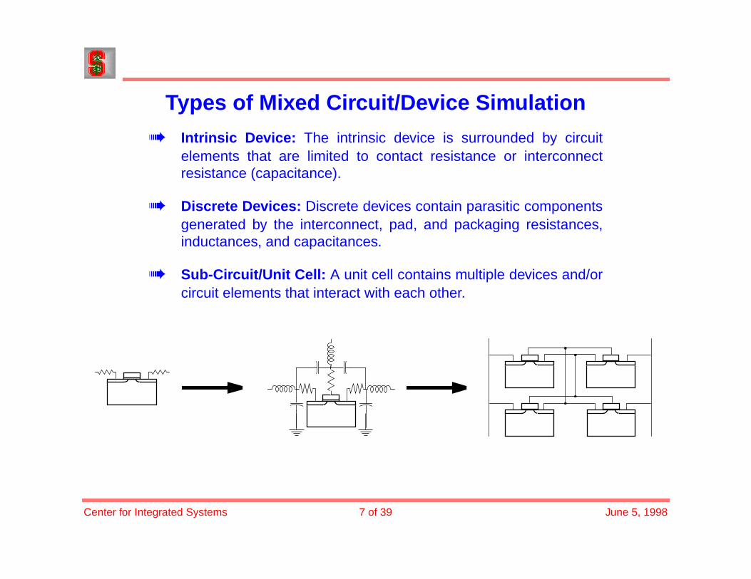
Types of Mixed Circuit/Device Simulation
Intrinsic Device: The intrinsic device is surrounded by circuitelements that are limited to contact resistance or interconnectresistance (capacitance).
Discrete Devices: Discrete devices contain parasitic componentsgenerated by the interconnect, pad, and packaging resistances,inductances, and capacitances.
Sub-Circuit/Unit Cell: A unit cell contains multiple devices and/orcircuit elements that interact with each other.
Center for Integrated Systems 8 of 39 June 5, 1998
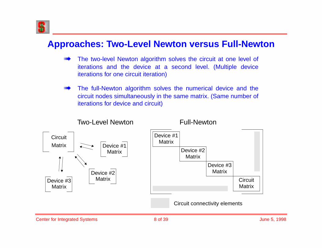
Approaches: Two-Level Newton versus Full-Newton
The two-level Newton algorithm solves the circuit at one level ofiterations and the device at a second level. (Multiple deviceiterations for one circuit iteration)
The full-Newton algorithm solves the numerical device and thecircuit nodes simultaneously in the same matrix. (Same number ofiterations for device and circuit)
Device #1Matrix
Full-NewtonTwo-Level Newton
Circuit
Matrix Device #1Matrix
Device #3Matrix
Device #2Matrix
Device #2Matrix
Device #3Matrix
CircuitMatrix
Circuit connectivity elements
Center for Integrated Systems 9 of 39 June 5, 1998
Comparison of the Two AlgorithmsAdvantages of the two-level Newton over the full-Newton algorithm:
Better convergence for DC analysis if node voltages are unknown.The full level Newton requires all circuit node voltages to bespecified within a certain percentage; otherwise it fails toconverge.
More modularity in two-level Newton allows many devicesimulators to be used simultaneously. For example, PISCES maybe used for two dimensional devices and Fielday may be used forthe three dimensional devices.
Easier to implement a parallel version of two-level Newtonalgorithm. Each numerical device simulation can be relegated to anode of a parallel machine whereas the matrix for the full levelNewton algorithm has to be partitioned to each node.
By utilizing SPICE as the circuit simulator, any improvements/modifications in SPICE automatically benefit the mixed-modesimulations.
Center for Integrated Systems 10 of 39 June 5, 1998
Comparison of the Two Algorithms (continued)Disadvantages of the two-level Newton over the full-Newton algorithm:
Given a good estimate of all the node voltages, the full-Newtonalgorithm converges much more quickly than the two-levelNewton.
Likewise, since transient analysis involves small voltage changesfrom time step to time step making the problem well behaved, thefull-Newton method converges much more quickly for this case aswell. Mayaram determined a factor of 1.7 times as fast.1
Limitations in scope of comparison:
Mayaram limited his devices to a couple hundred nodes, but as thesize of the problem increases, the dynamics change.
Work not presented in this talk explored the capabilities usingdevices of many nodes and using parallization.
1. Mayaram, Kartikeya and Donald O. Pederson. “Coupling Algorithms for Mixed-Level Circuit and Device Simulation.”IEEE Transactions on Computer Aided Design. Vol. II, No 8. August 1992. pp 1003-1012.
Center for Integrated Systems 11 of 39 June 5, 1998
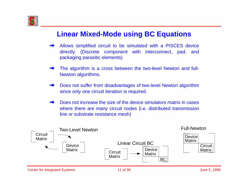
Linear Mixed-Mode using BC Equations
Allows simplified circuit to be simulated with a PISCES devicedirectly. (Discrete component with interconnect, pad, andpackaging parasitic elements)
The algorithm is a cross between the two-level Newton and full-Newton algorithms.
Does not suffer from disadvantages of two-level Newton algorithmsince only one circuit iteration is required.
Does not increase the size of the device simulators matrix in caseswhere there are many circuit nodes (i.e. distributed transmissionline or substrate resistance mesh)
CircuitMatrix
DeviceMatrix
DeviceMatrix
CircuitMatrixDevice
MatrixCircuitMatrix
BC
Full-NewtonTwo-Level Newton
Linear Circuit BC
Center for Integrated Systems 12 of 39 June 5, 1998
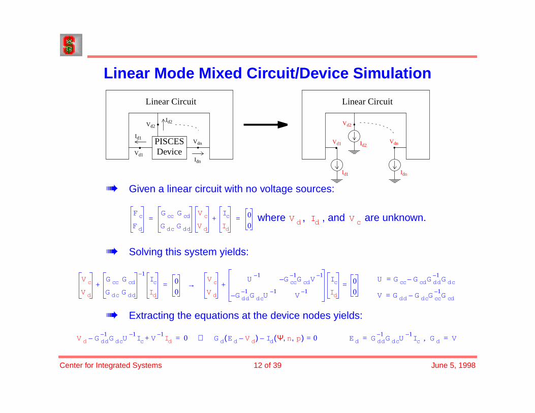
Linear Mode Mixed Circuit/Device Simulation
Given a linear circuit with no voltage sources:
where , , and are unknown.
Solving this system yields:
Extracting the equations at the device nodes yields:
PISCESDevice
Vd2
Vdn
Vd1
Id2
Idn
Id1
Linear Circuit
Vd2
VdnVd1 Id2
IdnId1
Linear Circuit
Fc
Fd
G cc G cd
G dc G dd
V c
V d
Ic
Id+ 0
0= = V d Id V c
V c
V d
G cc G cd
G dc G dd
1–Ic
Id+ 0
0
V c
V d
U1–
G cc1–G cdV
1––
G dd1–G dcU
1–– V
1–
Ic
Id+ 0
0
U G cc G cdG dd1–G dc–=
V G dd G dcG cc1–G cd–=
=→=
V d G dd1–G dcU
1–Ic– V
1–Id+ 0 G d E d V d–( ) Id Ψ n p, ,( )– 0 Ed=⇔ G dd
1–G dcU
1–Ic , G d V= = =
Center for Integrated Systems 13 of 39 June 5, 1998
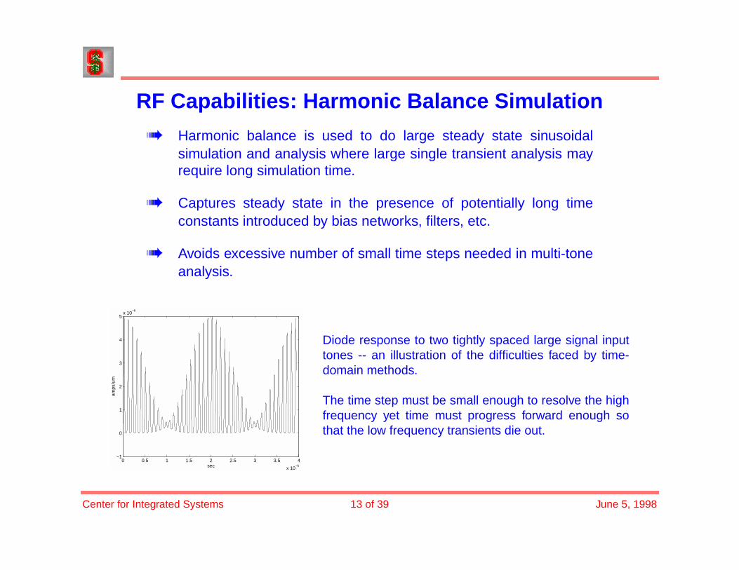
RF Capabilities: Harmonic Balance Simulation
Harmonic balance is used to do large steady state sinusoidalsimulation and analysis where large single transient analysis mayrequire long simulation time.
Captures steady state in the presence of potentially long timeconstants introduced by bias networks, filters, etc.
Avoids excessive number of small time steps needed in multi-toneanalysis.
0 0.5 1 1.5 2 2.5 3 3.5 4
x 10−6
−1
0
1
2
3
4
5x 10
−6
sec
amps
/um
Diode response to two tightly spaced large signal inputtones -- an illustration of the difficulties faced by time-domain methods.
The time step must be small enough to resolve the highfrequency yet time must progress forward enough sothat the low frequency transients die out.

Center for Integrated Systems 14 of 39 June 5, 1998
Harmonic Balance Solution1
Instead of solving for the time samples of each variable, theharmonic balance method expands each variable as a Fourierseries and solves for the coefficients:
The number of harmonics is limited to H. Harmonics of higherorder are assumed to be insignificant.
Harmonic balance solves for the real and imaginary coefficientswhich can then be assembled into a time domain representation ofthe signal in addition to the computed spectral view of the signal.
Using basic circuit theory techniques, power can be calculated inthe total signal or the individual harmonics.
1. For an in depth discussion of the solution algorithms please refer to the dissertation titled: Frequency DomainAlgorithms for Simulating Large Signal Distortion in Semiconductor Devices by Boris Troyanovsky.
xn t( ) X n0 X nhR ωht( )cos X nh
I ωht( )sin–( )h 1=
H
∑+=
Center for Integrated Systems 15 of 39 June 5, 1998
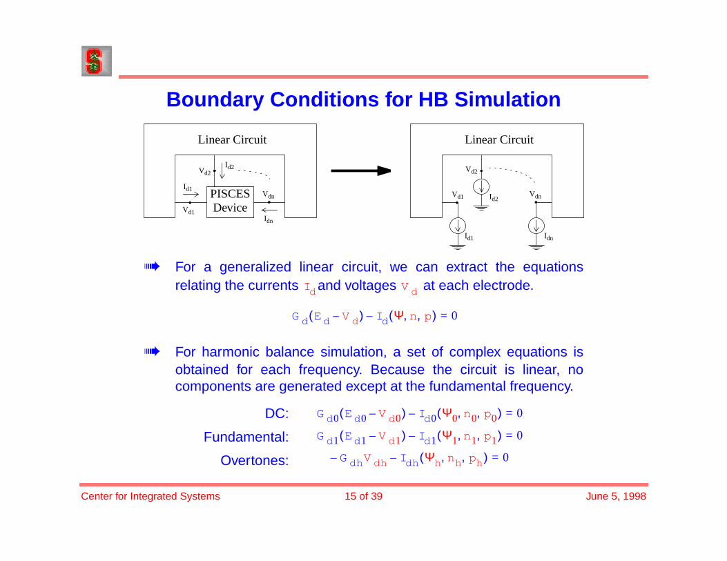
Boundary Conditions for HB Simulation
For a generalized linear circuit, we can extract the equationsrelating the currents and voltages at each electrode.
For harmonic balance simulation, a set of complex equations isobtained for each frequency. Because the circuit is linear, nocomponents are generated except at the fundamental frequency.
PISCESDevice
Vd2
Vdn
Vd1
Id2
Idn
Id1
Linear Circuit
Vd2
VdnVd1 Id2
IdnId1
Linear Circuit
Id V d
G d Ed V d–( ) Id Ψ n p, ,( )– 0=
G d0 Ed0 V d0–( ) Id0 Ψ0 n0 p0, ,( )– 0=
G d1 Ed1 V d1–( ) Id1 Ψ1 n1 p1, ,( )– 0=
G dhV dh– Idh Ψh nh ph, ,( )– 0=
DC:
Fundamental:
Overtones:
Center for Integrated Systems 16 of 39 June 5, 1998
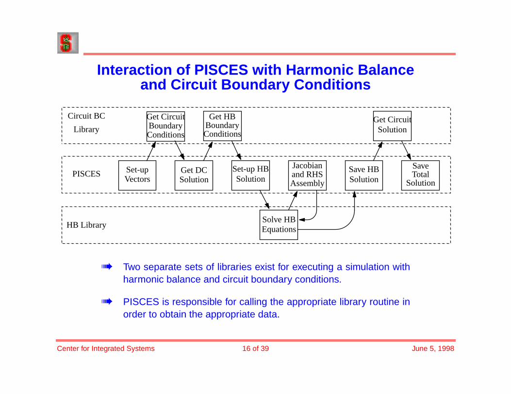
Interaction of PISCES with Harmonic Balanceand Circuit Boundary Conditions
Two separate sets of libraries exist for executing a simulation withharmonic balance and circuit boundary conditions.
PISCES is responsible for calling the appropriate library routine inorder to obtain the appropriate data.
PISCES
Circuit BC
HB Library
Library
Get HBBoundaryConditions
Set-upVectors
Get DCSolution
Set-up HBSolution
Solve HBEquations
Jacobianand RHSAssembly
Save HBSolution
Get CircuitSolution
SaveTotal
Solution
Get CircuitBoundaryConditions
Center for Integrated Systems 17 of 39 June 5, 1998
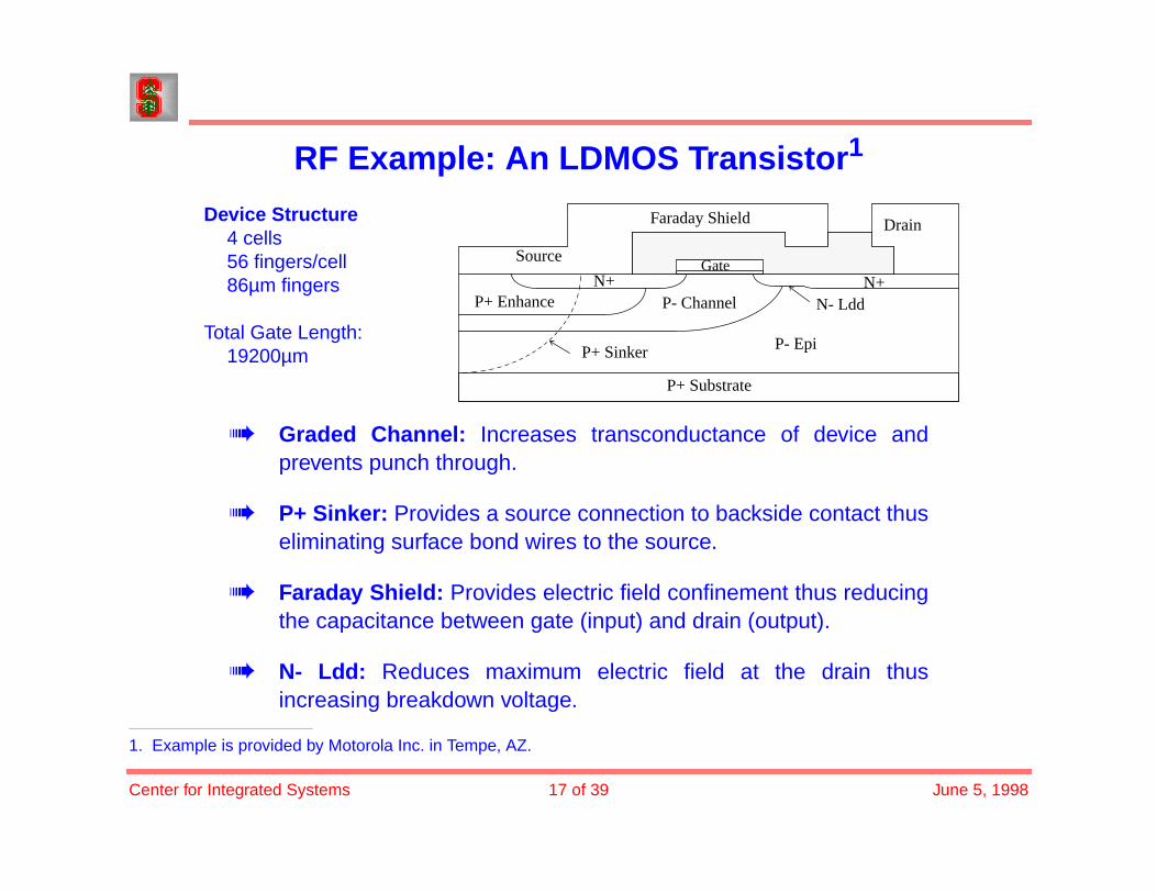
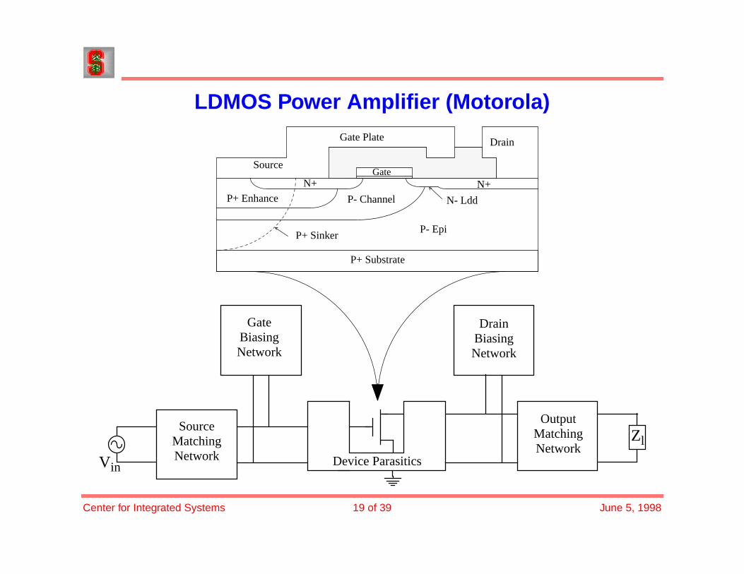
RF Example: An LDMOS Transistor1
Graded Channel: Increases transconductance of device andprevents punch through.
P+ Sinker: Provides a source connection to backside contact thuseliminating surface bond wires to the source.
Faraday Shield: Provides electric field confinement thus reducingthe capacitance between gate (input) and drain (output).
N- Ldd: Reduces maximum electric field at the drain thusincreasing breakdown voltage.
1. Example is provided by Motorola Inc. in Tempe, AZ.
Drain
GateSource
P+ Sinker
N+P- Channel
P- Epi
N- Ldd
N+P+ Enhance
Faraday Shield
P+ Substrate
Device Structure4 cells56 fingers/cell86µm fingers
Total Gate Length:19200µm
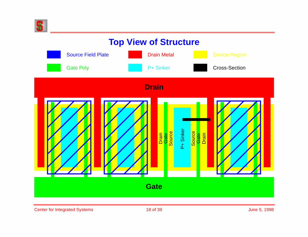
Center for Integrated Systems 18 of 39 June 5, 1998
Top View of StructureSource Field Plate
Gate Poly P+ Sinker
Drain Metal Device Region
Sou
rce
Dra
in
Dra
in
Sou
rce
Gat
e
P+
Sin
ker
Gat
e
Gate
Drain
Cross-Section
Center for Integrated Systems 19 of 39 June 5, 1998
LDMOS Power Amplifier (Motorola)
Zl
Vin
GateBiasingNetwork
DrainBiasingNetwork
SourceMatchingNetwork
OutputMatchingNetwork
Device Parasitics
Drain
GateSource
P+ Sinker
N+P- Channel
P- Epi
N- Ldd
N+
P+ Enhance
Gate Plate
P+ Substrate
Center for Integrated Systems 20 of 39 June 5, 1998
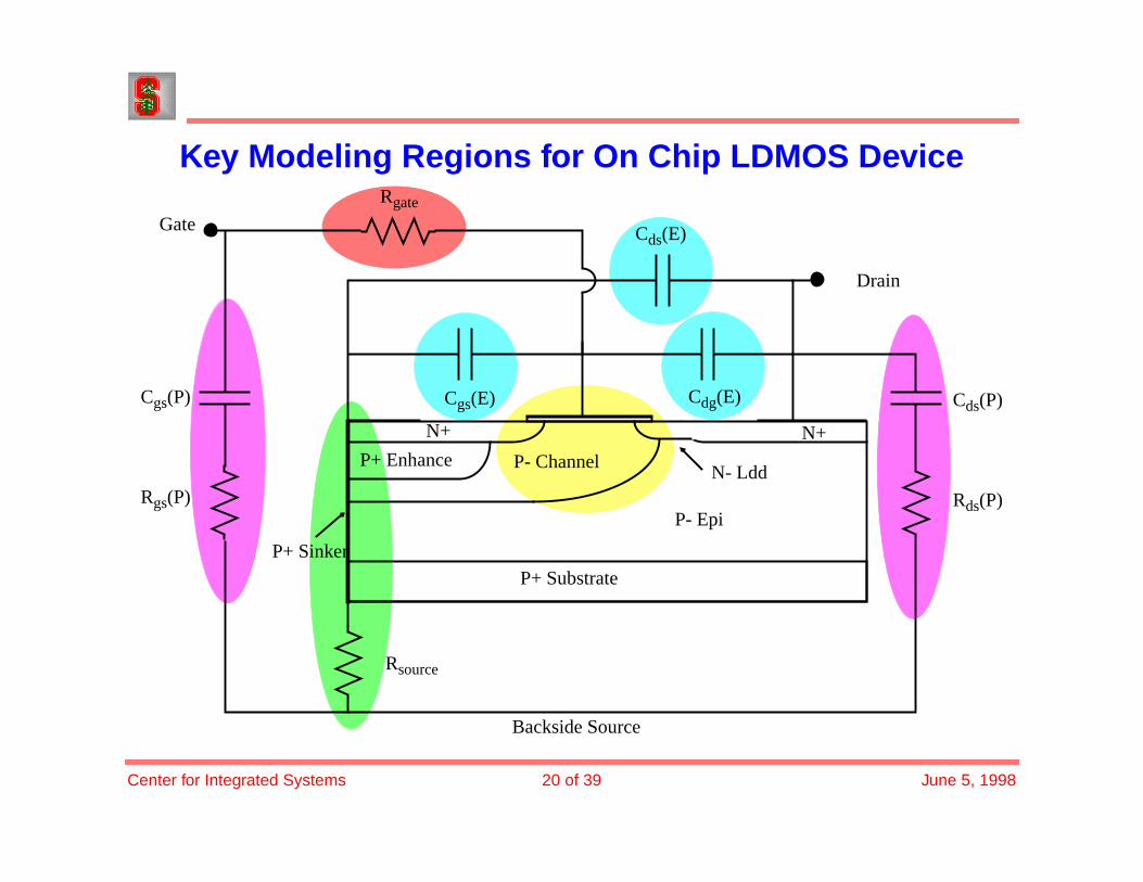
Key Modeling Regions for On Chip LDMOS Device
Drain
Gate
Backside Source
P+ Sinker
N+
P- Channel
P- Epi
N- Ldd
N+
P+ Enhance
P+ Substrate
Cgs(E)
Cds(E)
Cdg(E)
Rsource
Rgate
Cds(P)
Rds(P)
Cgs(P)
Rgs(P)
Center for Integrated Systems 21 of 39 June 5, 1998
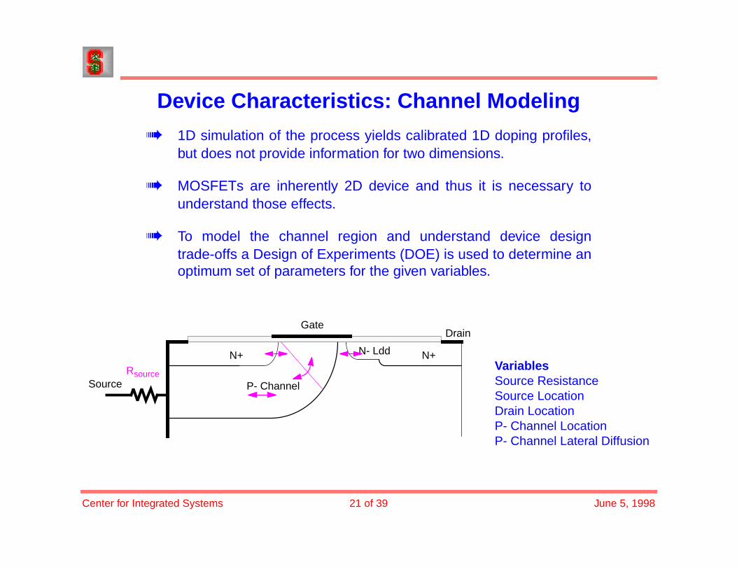
Device Characteristics: Channel Modeling
1D simulation of the process yields calibrated 1D doping profiles,but does not provide information for two dimensions.
MOSFETs are inherently 2D device and thus it is necessary tounderstand those effects.
To model the channel region and understand device designtrade-offs a Design of Experiments (DOE) is used to determine anoptimum set of parameters for the given variables.
N+ N- Ldd
P- Channel
N+
DrainGate
SourceRsource
VariablesSource ResistanceSource LocationDrain LocationP- Channel LocationP- Channel Lateral Diffusion
Center for Integrated Systems 22 of 39 June 5, 1998
Sensitivity Analysis of Graded Channel Region
Drain location had no effect on DC characteristics, but lateranalysis showed there was a significant effect on ACcharacteristics.
The measured Gm at high current is affected strongly by sourceresistance and source location.
Reason: The internal Vgs is reduced by the voltage drop acrossresistances on the source side of the device.
The measured Vt is affected strongly by channel location andsource location.
Reason: Threshold is determined by the inversion of the channelnearest the source side of the device.
The measured sub-threshold slope is affected strongly by sourcelocation and channel location.
Reason: The slope is determined by the channel length andpunch through characteristics.
Center for Integrated Systems 23 of 39 June 5, 1998
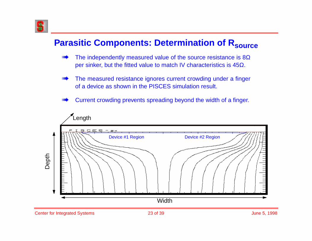
Parasitic Components: Determination of Rsource
The independently measured value of the source resistance is 8Ωper sinker, but the fitted value to match IV characteristics is 45Ω.
The measured resistance ignores current crowding under a fingerof a device as shown in the PISCES simulation result.
Current crowding prevents spreading beyond the width of a finger.
Dep
th
Width
Length
Device #1 Region Device #2 Region
Center for Integrated Systems 24 of 39 June 5, 1998
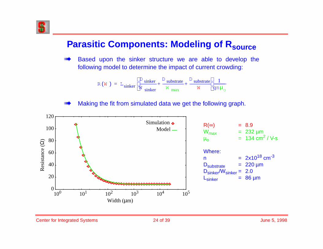
Parasitic Components: Modeling of Rsource
Based upon the sinker structure we are able to develop thefollowing model to determine the impact of current crowding:
Making the fit from simulated data we get the following graph.
R W( ) L sinker
D sinkerW sinker------------------
D substrateW max
-----------------------D substrate
W-----------------------+ +
1
qnµo-------------=
0
20
40
60
80
100
120
100 101 102 103 104 105
Res
ista
nce
(Ω)
Width (µm)
SimulationModel
R(∞) = 8.9Wmax = 232 µmµo = 134 cm2 / V-s
Where:n = 2x1018 cm-3
Dsubstrate = 220 µmDsinker/Wsinker = 2.0Lsinker = 86 µm
Center for Integrated Systems 25 of 39 June 5, 1998
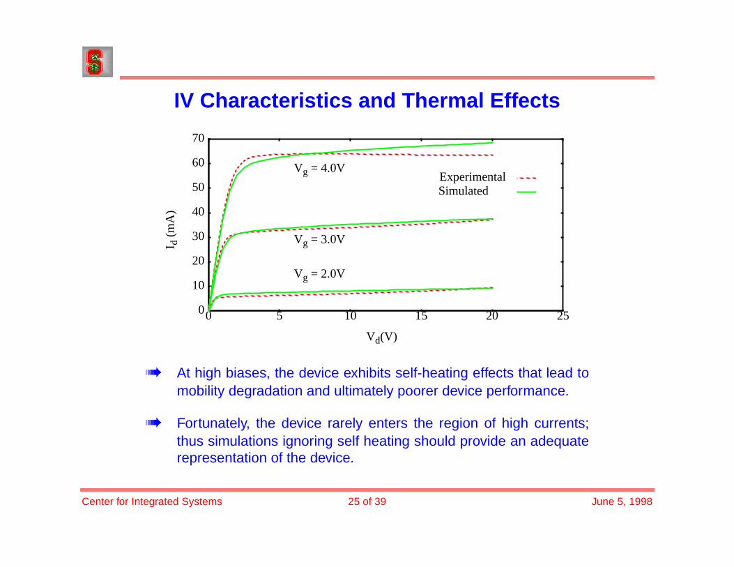
IV Characteristics and Thermal Effects
At high biases, the device exhibits self-heating effects that lead tomobility degradation and ultimately poorer device performance.
Fortunately, the device rarely enters the region of high currents;thus simulations ignoring self heating should provide an adequaterepresentation of the device.
0
10
20
30
40
50
60
70
0 5 10 15 20 25
SimulatedExperimental
I d (
mA
)
Vd(V)
Vg = 2.0V
Vg = 3.0V
Vg = 4.0V
Center for Integrated Systems 26 of 39 June 5, 1998
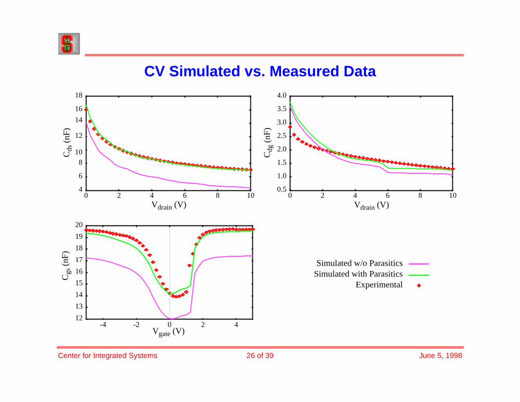
CV Simulated vs. Measured DataC
gs (
nF)
Cds
(nF
)
Cdg
(nF
)
Vgate (V)
Vdrain (V) Vdrain (V)
4
6
810
12
14
16
18
0 2 4 6 8 100.5
1.0
1.5
2.0
2.5
3.0
3.5
4.0
0 2 4 6 8 10
12
13
14
15
16
17
18
19
20
-4 -2 0 2 4
Simulated w/o ParasiticsSimulated with Parasitics
Experimental
Center for Integrated Systems 27 of 39 June 5, 1998
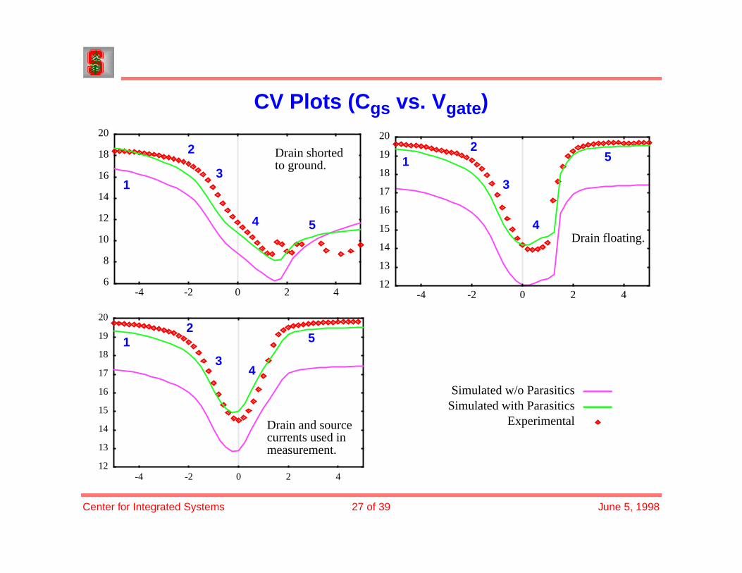
CV Plots (Cgs vs. Vgate)
Drain shortedto ground.
Drain floating.
Drain and sourcecurrents used inmeasurement.
12
13
14
15
16
17
18
19
20
-4 -2 0 2 46
8
10
12
14
16
18
20
-4 -2 0 2 4
12
13
14
15
16
17
18
19
20
-4 -2 0 2 4
Simulated w/o ParasiticsSimulated with Parasitics
Experimental
1
2
3
4
512
3
4
512
3
4 5
Center for Integrated Systems 28 of 39 June 5, 1998
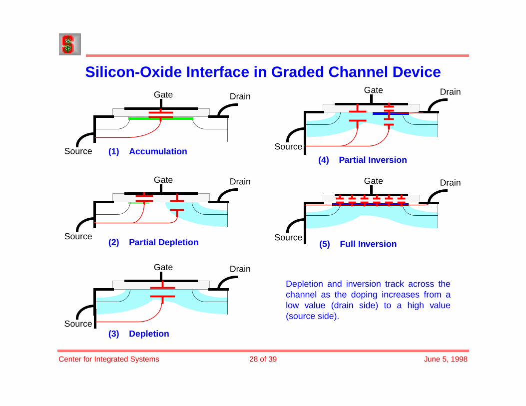
Silicon-Oxide Interface in Graded Channel DeviceGate Drain
Source
Gate Drain
Source
Gate Drain
Source
Gate Drain
Source
Gate Drain
Source
(1) Accumulation
(2) Partial Depletion
(3) Depletion
(4) Partial Inversion
(5) Full Inversion
Depletion and inversion track across thechannel as the doping increases from alow value (drain side) to a high value(source side).
Center for Integrated Systems 29 of 39 June 5, 1998
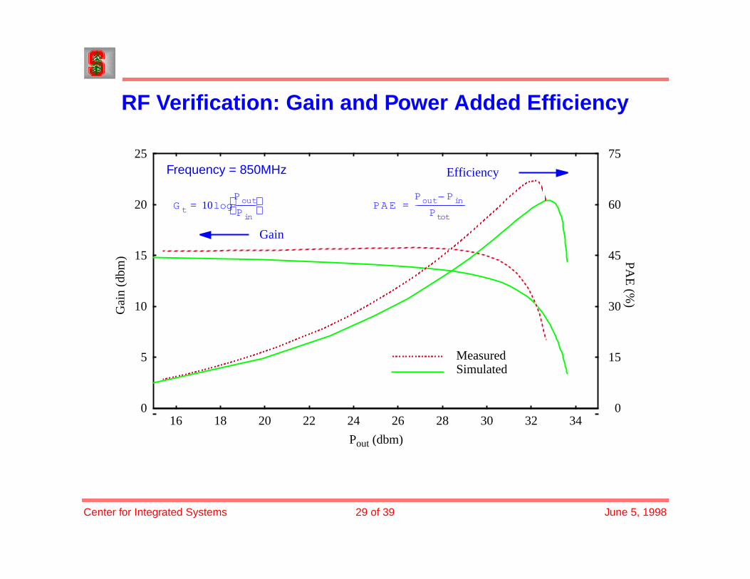
RF Verification: Gain and Power Added Efficiency
0
15
30
45
60
75
16 18 20 22 24 26 28 30 32 340
5
10
15
20
25
MeasuredSimulated
Efficiency
Gain
Pout (dbm)
PAE
(%)
Gai
n (d
bm)
Frequency = 850MHz
PAEPout Pin–
Ptot---------------------------=G t 10
PoutPin-----------
log=
Center for Integrated Systems 30 of 39 June 5, 1998
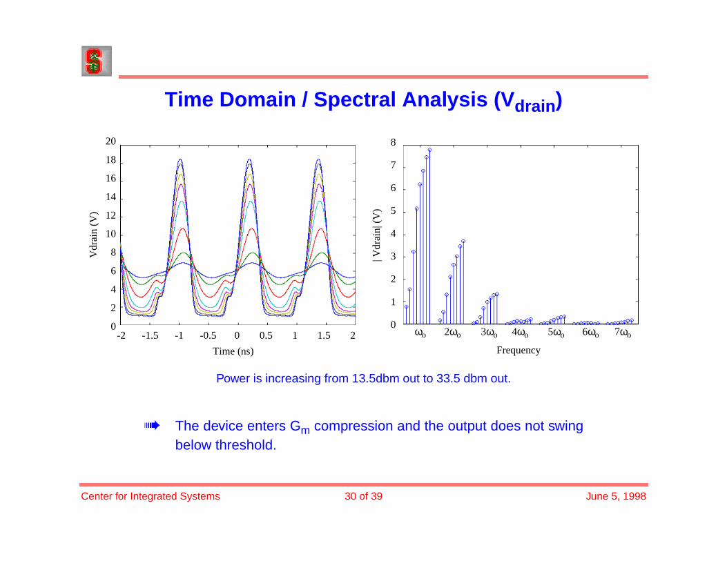
Time Domain / Spectral Analysis (Vdrain)
The device enters Gm compression and the output does not swingbelow threshold.
0
2
4
6
8
10
12
14
16
18
20
-2 -1.5 -1 -0.5 0 0.5 1 1.5 20
1
2
3
4
5
6
7
8
ωo 2ωo 3ωo 4ωo 5ωo
Vdr
ain
(V)
Time (ns) Frequency
| Vdr
ain|
(V
)
6ωo 7ωo
Power is increasing from 13.5dbm out to 33.5 dbm out.
Center for Integrated Systems 31 of 39 June 5, 1998
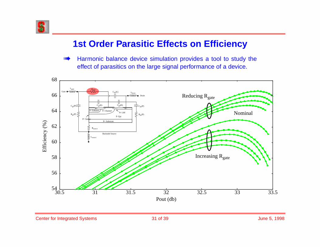
1st Order Parasitic Effects on Efficiency
Harmonic balance device simulation provides a tool to study theeffect of parasitics on the large signal performance of a device.
54
56
58
60
62
64
66
68
30.5 31 31.5 32 32.5 33 33.5
Eff
icie
ncy
(%)
Pout (db)
Reducing Rgate
Nominal
Increasing Rgate
Drain
Gate
Backside Source
P+ Sinker
N+P- Channel
P- Epi
N- Ldd
N+P+ Enhance
P+ Substrate
Cgs(E)
Cds(E)
Cgd(E)
Rsource
Rgate
Cds(P)
Rds(P)
Cgs(P)
Rgs(P)
Ldrain
Lsource
Lgate

Center for Integrated Systems 32 of 39 June 5, 1998
2nd Order Parasitic Effects on Efficiency
Examining the curves where Rgate is reduced yields anunderstanding of the second order effects.
63
64
65
66
67
68
32 32.2 32.4 32.6 32.8 33 33.2 33.4
Eff
icie
ncy
(%)
Pout (db)
Reducing Cgs
Reducing Rgate
Reducing Lsource
Reducing Lsource
Increasing Cgs
Increasing Lsource
Increasing Lsource
Drain
Gate
Backside Source
P+ Sinker
N+P- Channel
P- Epi
N- Ldd
N+P+ Enhance
P+ Substrate
Cgs(E)
Cds(E)
Cgd(E)
Rsource
Rgate
Cds(P)
Rds(P)
Cgs(P)
Rgs(P)
Ldrain
Lsource
Lgate
Center for Integrated Systems 33 of 39 June 5, 1998
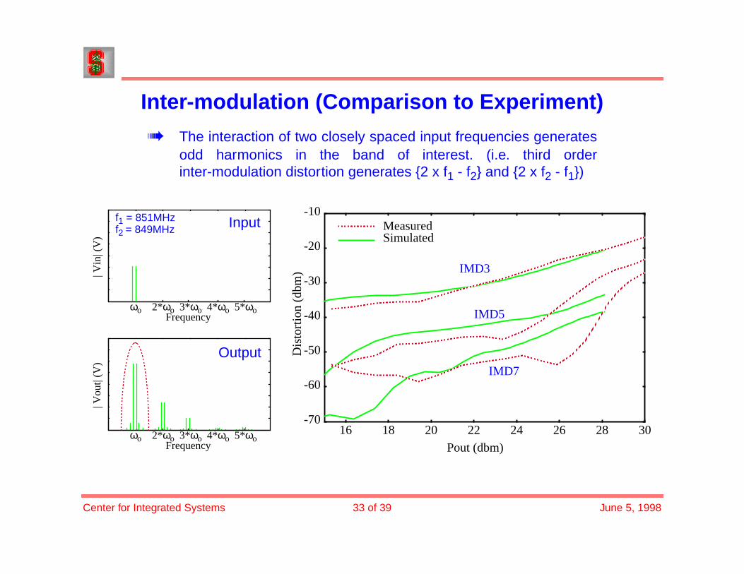
Inter-modulation (Comparison to Experiment)
The interaction of two closely spaced input frequencies generatesodd harmonics in the band of interest. (i.e. third orderinter-modulation distortion generates 2 x f1 - f2 and 2 x f2 - f1)
-70
-60
-50
-40
-30
-20
-10
16 18 20 22 24 26 28 30
IMD3
IMD5
IMD7
Pout (dbm)
MeasuredSimulated
Dis
tort
ion
(dbm
)
ωo 2*ωo 3*ωo 4*ωo 5*ωoFrequency
| Vou
t| (V
)
ωo 2*ωo 3*ωo 4*ωo 5*ωoFrequency
| Vin
| (V
)
Input
Output
f1 = 851MHzf2 = 849MHz
Center for Integrated Systems 34 of 39 June 5, 1998
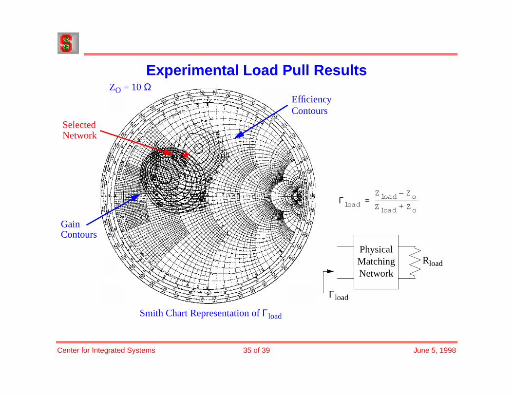
Matching Network Effects
Matching networks play a critical role in efficiently transferringpower from the supply source to the amplifier and from theamplifier to the load.
The input matching network is designed to reduce reflections backto the supply thus preventing wasted power.
The output network has multiple functions:
a. Impedance matching between amplifier output and load to achievemaximum power transfer.
b. Filter for higher order harmonics.
A load-pull analysis is used to sweep over multiple matchingnetworks configurations and to calculate gain and efficiency foreach of those configurations.
a. Input power is set to a constant value.
b. Input matching network is set to minimize reflections.
c. Output matching network is swept.
d. Contour plots for gain and efficiency are plotted
Center for Integrated Systems 35 of 39 June 5, 1998
Experimental Load Pull Results
Gain
EfficiencyZO = 10 Ω
Contours
Contours
SelectedNetwork
PhysicalMatchingNetwork
Rload
Γload
Smith Chart Representation of Γload
ΓloadZload Zo–
Zload Zo+-----------------------------=
Center for Integrated Systems 36 of 39 June 5, 1998
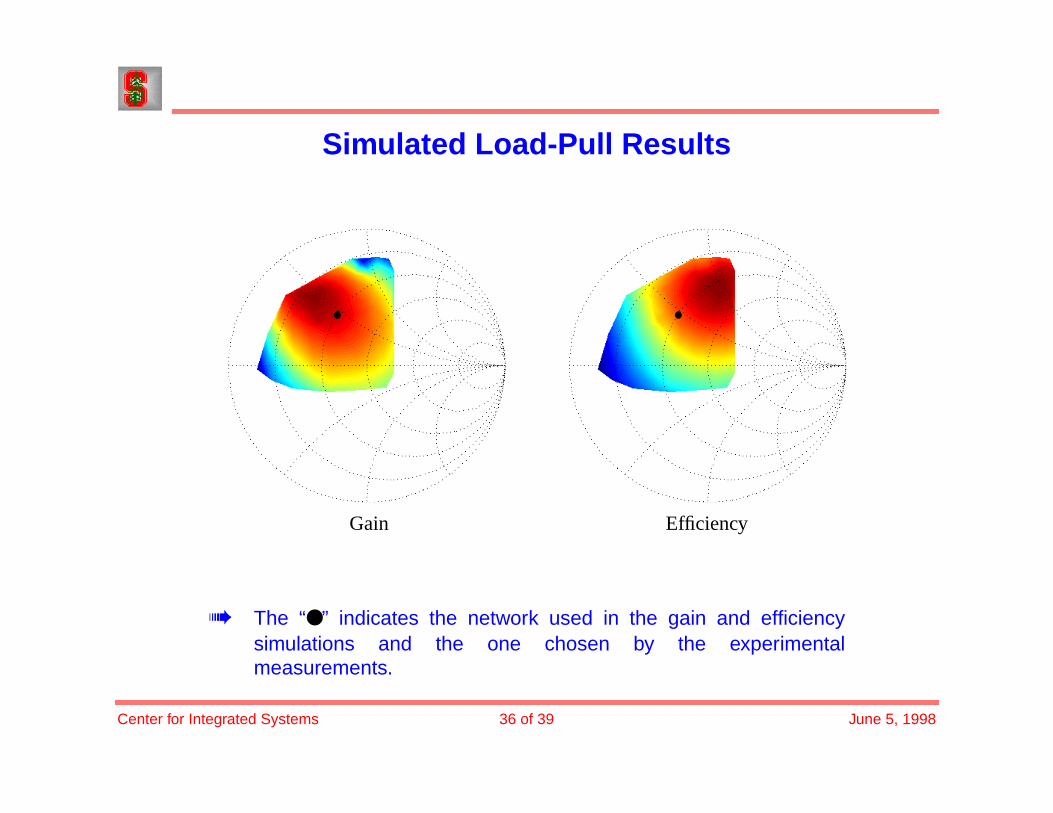
Simulated Load-Pull Results
The “ ” indicates the network used in the gain and efficiencysimulations and the one chosen by the experimentalmeasurements.
Gain Efficiency

Center for Integrated Systems 37 of 39 June 5, 1998
Contributions
Extended work on mixed circuit and device simulation for use withlarger and more realistic problems. (not presented)
Parallelized mixed circuit and device simulation so that largeproblems can be solved on a network of workstations. (notpresented)
Improved PISCES to include a generalized linear circuit throughboundary condition equations.
Integrated PISCES with an harmonic balance solver anddeveloped the boundary condition equations for harmonic balanceanalysis with circuit components.
Modeled RF LDMOS devices for use in device simulation toprovide predictive analysis.
Developed tools and methodologies to aid in RF devicedesign by including the intrinsic physical device with externalparasitics and matching networks.
Center for Integrated Systems 38 of 39 June 5, 1998
Acknowledgments Kunle Olukotun: Special thanks for taking the time to chair my orals.
Bob Dutton: My advisor and mentor at Stanford University.
Simon Wong: My associate advisor and one of the first professors that I metat Stanford through EE216 and EE410.
Zhiping Yu: A very important mentor who is a gold mine of knowledge.
Gordon Ma: Motorola mentor who provided help and expertise inunderstanding LDMOS devices and RF device design.
Boris Troyanovsky: Former TCAD student (currently at HP) who providedinvaluable assistance in understanding HB solvers.
Sunderarajan Sunderesan Mohan: A good friend and a knowledgeableperson who was able to answer my many questions about RF.
SRC and ARO: Funding agencies that supported me through the Ph.D.program at Stanford.

Center for Integrated Systems 39 of 39 June 5, 1998
Acknowledgments (continued) Fely & Maria & (Lynn): Professor Dutton’s administrative staff who provided
much needed guidance through Stanford’s bureaucracy.
TCADre (past and present): The many members of Bob Dutton’s group withwhom I have interacted: both technically and socially.
Stanford Volleyball Program: Provided an escape from the rigors of the Ph.D.world. I would especially like to acknowledge Reuben Nieves for his manyyears of excellent instruction.
CroMem: There are many people whom I met from my years living inCroMem. Many have left a lasting impression.
Joe & Jerrie Ann: My brother and his wife who have made the long trek fromBoston to California to be here today.
Friends: They provided the laughs and camaraderie to make it through thedifficult times and shared in the many fun times.