Embed Size (px)
Citation preview
Lehrstuhl fur Technische ElektronikTechnische Universitat Munchen • Arcisstraße 21 • 80333 MunchenTel: 089/289-22929 • Fax: 089/289-22938 • Email: [email protected]
Prof. Dr. rer. nat. Franz Kreupl
Mixed-Signal IC Design LAB
LTE, SS 2017Prof. Dr. rer. nat. Franz Kreupl
M.Sc. Andrew GiebfriedM.Sc. Umidjon Nurmetov
LAB Introduction
There are 3 Labs to choose from:
1. 1st Order 1-Bit Σ∆-ADC for Audio Applications:In this lab, you will design a 1st order Σ∆-ADC able to process signals for voiceapplications from system level to circuit level. This lab will have an emphasis onsignal processing and system level design.
2. Algorithmic ADC for Sensor Applications:In this lab, you will design an algorithmic ADC following a given specification fromsystem level to circuit level. This lab will have an emphasis on designing withswitched-cap circuits and the transistor-level design.
3. Successive Approximation ADC for Sensor Applications:In this lab, you will design a sucessive approximation ADC following a given spec-ification from system level to circuit level. This lab will have an emphasis on usingdifferent Cadence tools throughout the entire design process. The control logic forthis ADC will be implemented with either Verilog or VHDL.
2
Rules and Suggestions in the Labs:
1. Deliverables:
• A “Design Report” comprising of three parts should be handed in. It shouldbe properly formatted (e.g. written in LATEX or a properly formatted Worddocument.) The first part should be completed by May 12, the second partJune 12, and the last part August 31. The report should be written as-suming the reader has taken a Mixed-Signal course, but is not necessarily anexpert.
• A 15 minute presentation will take place on Late July, where each groupshows their outcomes up to that point.
• Your Simulink model, any MATLAB scripts used, your HDL code (if appli-cable), and the Cadence schematics and ADE states used to simulate yourresults. These should be delivered when the relevent section of the report isdue.
2. Teamwork: Each topic has two or three participants. Please make sure you arein good relationship and achieve the final goal together. The division of labour isdetermined by each group themselves.
3. Lab usage: The lab room (N4303) is open Monday to Friday during office hours(8:00 - 19:00). These computers can also be accessed from any Linux machine on theLRZ network via SSH from the using the command ssh -X [groupname]@[ip-address]
where groupname is the groupname given to you and ip-address is one of the ipaddresses printed on the lab computers. Since another group might also using thesame machine remotely, please do not shutdown the computer, just log off. Forsecurity purposes, these machines will not read USB drives.
4. Grading: The three reports and the final presentation are graded, not only interms of its content, but also considering their quality and clarity.
Reference Books
• D.A. Johns; K. Martin, Analog Integrated Circuit Design, Wiley, 1997
• B. Razavi, Design of Analog CMOS Integrated Circuits, McGraw-Hill, 2001
• R. Schreier; G.C. Temes, Understanding Delta-Sigma Data Converters, IEEE Press, 2005
• S.R. Norsworthy; R. Schreier, Delta-Sigma Data Converters, IEEE Press, 1997
• A.V. Oppenheim; A.S. Willsky, Signals and Systems, Prentice Hall, 1999
• R.J. Baker; H.W. Li; D.E. Boyce, CMOS, Circuit Design, Layout and Simulation, Wiley, 1997
• R. Gregorian; G.C. Temes, Analog MOS Integrated Circuits For Signal Processing, Wiley, 1986
• S.J. Orfanidis, Introduction to Signal Processing, Prentice Hall, 1998
3
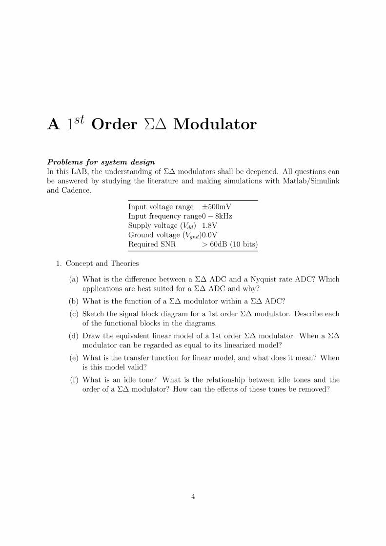
A 1st Order Σ∆ Modulator
Problems for system designIn this LAB, the understanding of Σ∆ modulators shall be deepened. All questions canbe answered by studying the literature and making simulations with Matlab/Simulinkand Cadence.
Input voltage range ±500mVInput frequency range0− 8kHzSupply voltage (Vdd) 1.8VGround voltage (Vgnd)0.0VRequired SNR > 60dB (10 bits)
1. Concept and Theories
(a) What is the difference between a Σ∆ ADC and a Nyquist rate ADC? Whichapplications are best suited for a Σ∆ ADC and why?
(b) What is the function of a Σ∆ modulator within a Σ∆ ADC?
(c) Sketch the signal block diagram for a 1st order Σ∆ modulator. Describe eachof the functional blocks in the diagrams.
(d) Draw the equivalent linear model of a 1st order Σ∆ modulator. When a Σ∆modulator can be regarded as equal to its linearized model?
(e) What is the transfer function for linear model, and what does it mean? Whenis this model valid?
(f) What is an idle tone? What is the relationship between idle tones and theorder of a Σ∆ modulator? How can the effects of these tones be removed?
4
2. Spectrum analysis
(a) What is the Discrete Fourier Transform? What is the equation that definesit?
(b) MATLAB does not provide a DFT() function; instead it provides the similarfunction FFT(). What is the relationship between these two functions?
(c) Briefly explain what a ‘window function’ is. Why is it used and how does itaffect the results?
(d) How is the SNR of a sinusoidal input calculated from the DFT? Write a MAT-LAB function to calculate this.
(Finish the problems above before May 12 and submit the report toyour supervisor)
3. System development and analysis
(a) Determine the minimum required OSR needed to implement the required SNRwith a first order Σ∆ modulator.
(b) Prototype a first-order Σ∆ modulator in Simulink.
(c) Plot a sinusoidal input with the maximum possible amplitude and the resultingoutput signal over time on the same graph. Describe and interpret your results.
(d) Transform the output signal with the help of FFT in the frequency domain.Display the whole spectrum in the range from −1
2fs ≤ f ≤ 1
2fs, where fs is
the sample rate and baseband bandwidth. Describe and interpret your result.Think about the attributes a Σ∆ modulator should have. Do your resultsfulfill this requirements?
(e) Is the SNR dependent on the amplitude of the input signal? Justify youranswer and verify it via simulations. Make a diagram of SNR over the inputlevel.
(f) Use a constant input signal Vin = 13V . Simulate the system and analyse the
output signal in the time and frequency domain. What undesired effects occurand why do they occur?
(g) Design and implement a strategy that reduces this problem. Test your im-plementation via simulations and compare the results. What are the maindownsides to this solution?
(Finish above problems before June 12 and submit the report togetherwith the codes and simulation results to your supervisor)
5
Implementing and testing
4. You will now implement your Simulink prototype in Cadence Virtuoso in two iter-ations. In the first iteration, you will create an circuit using (mostly) ideal com-ponents. Then you will replace these ideal components with transistors for a morerealistic circuit. Please implement your design using a switched-capacitor approach.
(a) Based on your Simulink model, how can you split up your design into man-agable blocks? Create a cell for each of these blocks as well as a cell for an idealswitch. How can you verify that each of these blocks are properly functioning?
(b) The thermal noise of a capacitor will set a limit on the sampling capacitance fora switched-cap circuit. Determine the minimum required sampling capacitanceCs so that the RMS noise is less than ½LSB.
(c) Switched capacitor circuits are usually clocked with two alternating phases Φ1
and Φ2. How are these clocks generated and why is it not a good idea to usejust one clock signal and an inverter?
Verify that the circuit behaviour is correct using the same input signals used inyour Simulink model.
Note that the ½LSB here is one half the least significant bit of the signal after the deci-mation filter and downsampling is applied!
!Cadence’s default settings for transient simulationscan create excessive data and long simulation times.Set the strobeperiod and strobedelay parametersto more sensible values, if needed. You can find thesesettings in the transient simulation settings by press-ing Options... then navigating to the Output tab.
6

5. Once the circuit works with ideal components, work on the “transistor-level” im-plementation. In this iteration, you should replace the ideal components with morerealistic components. You should also use non-ideal OpAmps; however, a transistor-level description is not necessary: adjusting the cell parameters to more realisticvalues is sufficient.
(a) What non-ideal behaviour is introduced by using transistors instead of idealswitches? Which type of switch (NMOS, transmission gate, etc...) is bestsuited for this ADC?
(b) How does a finite gain of a real OpAmp affect the result? Calculate the mini-mum DC-gain for the OpAmp to ensure an error of less than ½LSB (ignoringthe thermal noise and finite bandwidth).
(c) How does a finite bandwidth affect the result? Calculate the required band-width for the OpAmps so the settling error over is less than ½LSB (ignoringthe finite gain and the thermal noise).
Apply the same input signals as before to your circuit. Compare these results toyour Simulink results. What is the final SNR of your circuit and where is the sourceof this noise?
!Please save the settings for for all of the simulationsyou use for your report! Go to Session→Save State...,then select Cellview at the top of the dialog. Thenunder Cellview Options give a meaningful name forState and a brief description of the test under De-scription.
(Finish above problems before August 31 and submit the report togetherwith the simulation files and results to your supervisor)
7
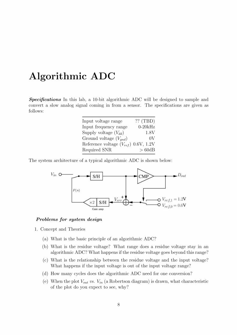
Algorithmic ADC
Specifications In this lab, a 10-bit algorithmic ADC will be designed to sample andconvert a slow analog signal coming in from a sensor. The specifications are given asfollows:
Input voltage range ?? (TBD)Input frequency range 0-20kHzSupply voltage (Vdd) 1.8VGround voltage (Vgnd) 0VReference voltage (Vref ) 0.6V, 1.2VRequired SNR > 60dB
The system architecture of a typical algorithmic ADC is shown below:
Problems for system design
1. Concept and Theories
(a) What is the basic principle of an algorithmic ADC?
(b) What is the residue voltage? What range does a residue voltage stay in analgorithmic ADC? What happens if the residue voltage goes beyond this range?
(c) What is the relationship between the residue voltage and the input voltage?What happens if the input voltage is out of the input voltage range?
(d) How many cycles does the algorithmic ADC need for one conversion?
(e) When the plot Vout vs. Vin (a Robertson diagram) is drawn, what characteristicof the plot do you expect to see, why?
8
2. Spectrum analysis
(a) What is the Discrete Fourier Transform? What is the equation that definesit?
(b) MATLAB does not provide a DFT() function; instead it provides the similarfunction FFT(). What is the relationship between these two functions?
(c) Briefly explain what a ‘window function’ is. Why is it used and how does itaffect the results?
(d) How is the SNR of a sinusoidal input calculated from the DFT? Write a MAT-LAB function to calculate this.
(Finish above problems before May 12 and submit the report to yoursupervisor)
3. Specification related
(a) Given the two reference voltages above, determine the input voltage range.
(b) Determine the required number of cycles corresponding to one conversion andsampling frequency fs according to the given specification.
(c) Prototype the behavioural model for the algorithmic ADC using Simulink.
(d) Draw the Robertson diagram showing the conversion process of your prototypewhen a constant, DC input is applied.
(e) Add gain error to the ×2 block. Draw the Robertson plot again. Whathappens this time? What about a negative gain error?
(f) Plot the output spectrum for a periodical sinusoidal input voltage. How muchis the noise floor below the input signal? Compare the simulated SNR to yourSNR calculations.
(Finish above problems before June 12 and submit the report togetherwith the codes and simulation results your supervisor)
9

Problems for circuit design
4. You will now implement your Simulink prototype in Cadence Virtuoso in two iter-ations. In the first iteration, you will create an circuit using (mostly) ideal com-ponents. Then you will replace these ideal components with transistors for a morerealistic circuit. Please implement your design using a switched-capacitor approach.
(a) Based on your Simulink model, how can you split up your design into man-agable blocks? Create a cell for each of these blocks as well as a cell for an idealswitch. How can you verify that each of these blocks are properly functioning?
(b) The thermal noise of a capacitor will set a limit on the sampling capacitance fora switched-cap circuit. Determine the minimum required sampling capacitanceCs so that the RMS noise is less than ½LSB.
(c) Switched capacitor circuits are usually clocked with two alternating phases Φ1
and Φ2. How are these clocks generated and why is it not a good idea to usejust one clock signal and an inverter?
Verify that the circuit behaviour is correct using the same input signals used inyour Simulink model.
!Cadence’s default settings for transient simulationscan create excessive data and long simulation times.Set the strobeperiod and strobedelay parametersto more sensible values, if needed. You can find thesesettings in the transient simulation settings by press-ing Options... then navigating to the Output tab.
10

5. Once the circuit works with ideal components, work on the “transistor-level” im-plementation. In this iteration, you should replace the ideal components with morerealistic components. You should also use non-ideal OpAmps; however, a transistor-level description is not necessary: adjusting the cell parameters to more realisticvalues is sufficient.
(a) What non-ideal behaviour is introduced by using transistors instead of idealswitches? Which type of switch (NMOS, transmission gate, etc...) is bestsuited for this ADC?
(b) How does a finite gain of a real OpAmp affect the result? Calculate the mini-mum DC-gain for the OpAmp to ensure an error of less than ½LSB (ignoringthe thermal noise and finite bandwidth).
(c) How does a finite bandwidth affect the result? Calculate the required band-width for the OpAmps so the settling error over is less than ½LSB (ignoringthe finite gain and the thermal noise).
Apply the same input signals as before to your circuit. Compare these results toyour Simulink results. What is the final SNR of your circuit and where is the sourceof this noise?
!Please save the settings for for all of the simulationsyou use for your report! Go to Session→Save State...,then select Cellview at the top of the dialog. Thenunder Cellview Options give a meaningful name forState and a brief description of the test under De-scription.
(Finish above problems before August 31 and submit the report togetherwith the simulation files and results to your supervisor)
11
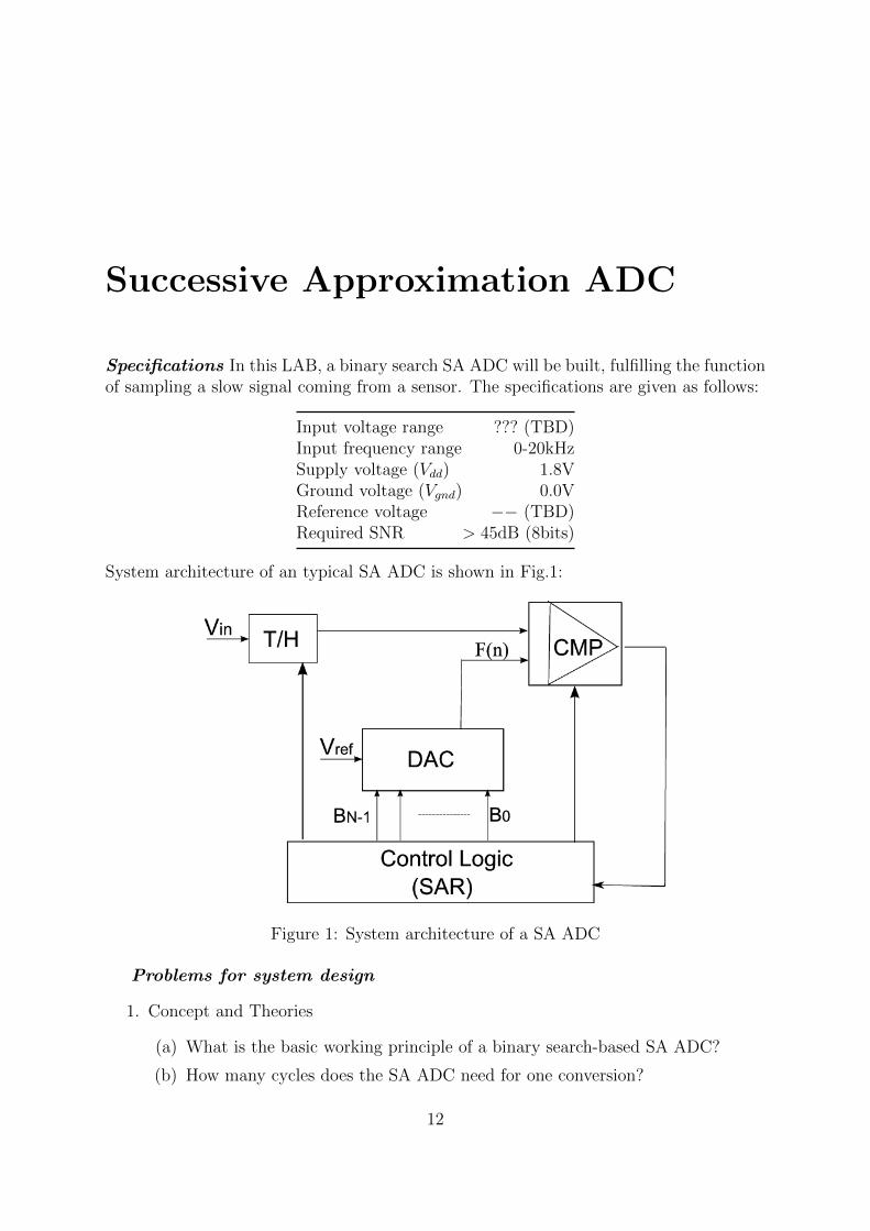
Successive Approximation ADC
Specifications In this LAB, a binary search SA ADC will be built, fulfilling the functionof sampling a slow signal coming from a sensor. The specifications are given as follows:
Input voltage range ??? (TBD)Input frequency range 0-20kHzSupply voltage (Vdd) 1.8VGround voltage (Vgnd) 0.0VReference voltage −− (TBD)Required SNR > 45dB (8bits)
System architecture of an typical SA ADC is shown in Fig.1:
Figure 1: System architecture of a SA ADC
Problems for system design
1. Concept and Theories
(a) What is the basic working principle of a binary search-based SA ADC?
(b) How many cycles does the SA ADC need for one conversion?
12
(c) Compare an SA ADC that uses a binary code against one with a thermometercode.
(d) What are the advantages of a Hybrid ADC?
(e) What are the advantages of using charge distribution DAC in SA ADC?
(f) Which circuit elements in the SA ADC cause DNL and INL errors? State theequation describing relation between INL and DNL errors.
(g) What is the maximum achievable theoretical SNR for an N bit ADC? Why isthe ENOB always less than designed resolution of an ADC?
2. Spectrum analysis
(a) What is the Discrete Fourier Transform? What is the equation that definesit?
(b) MATLAB does not provide a DFT() function; instead it provides the similarfunction FFT(). What is the relationship between these two functions?
(c) Briefly explain what a ‘window function’ is. Why is it used and how does itaffect the results?
(d) How is the SNR of a sinusoidal input calculated from the DFT? Write a MAT-LAB function to calculate this.
(Please finish above problems before May 12.)
3. Specification related
(a) Draw a finite state machine for the control logic (SAR) block for the SAADC using a Hybrid DAC with D bits using a thermometer code and theremaining B−D bits using a binary code. You do not need to show the FSMfor any counters, shift registers, etc. that you may use for the SAR.
(b) Using VHDL or Verilog, implement the code for the SAR.
(c) Determine the reference voltage and the input voltage range. Let D = 3 bits.
(d) Determine the required number of cycles corresponding to one conversion andsampling frequency fs according to the given specification.
(e) Implement the rest of the ADC using Simulink. You should use the “HDLCosimulation” block so your VHDL/Verilog code is used for the SAR.
(f) If a constant DC input is given, plot F (n) vs. time. What characteristic isshown in such a plot?
(Please finish above problems before June 12.)
13
Problems for circuit design
4. You will now implement your Simulink prototype in Cadence Virtuoso in two iter-ations. In the first iteration, you will create an circuit using (mostly) ideal com-ponents. Then you will replace these ideal components with transistors for a morerealistic circuit. Please implement your design using a switched-capacitor approach.
(a) Based on your Simulink model, how can you split up your design into man-agable blocks? Create a cell for each of these blocks as well as a cell for an idealswitch. How can you verify that each of these blocks are properly functioning?
(b) The thermal noise of a capacitor will set a limit on the sampling capacitance fora switched-cap circuit. Determine the minimum required sampling capacitanceCs so that the RMS noise is less than ½LSB.
(c) Switched capacitor circuits are usually clocked with two alternating phases Φ1
and Φ2. How are these clocks generated and why is it not a good idea to usejust one clock signal and an inverter?
Verify that the circuit behaviour is correct using the same input signals used inyour Simulink model.
!Cadence’s default settings for transient simulationscan create excessive data and long simulation times.Set the strobeperiod and strobedelay parametersto more sensible values, if needed. You can find thesesettings in the transient simulation settings by press-ing Options... then navigating to the Output tab.
14
5. Once the circuit works with ideal components, work on the “transistor-level” im-plementation. In this iteration, you should replace the ideal components with morerealistic components. You should also use non-ideal OpAmps; however, a transistor-level description is not necessary: adjusting the cell parameters to more realisticvalues is sufficient.
(a) What non-ideal behaviour is introduced by using transistors instead of idealswitches? Which type of switch (NMOS, transmission gate, etc...) is bestsuited for this ADC?
(b) How does a finite gain of a real OpAmp affect the result? Calculate the mini-mum DC-gain for the OpAmp to ensure an error of less than ½LSB (ignoringthe thermal noise and finite bandwidth).
(c) How does a finite bandwidth affect the result? Calculate the required band-width for the OpAmps so the settling error over is less than ½LSB (ignoringthe finite gain and the thermal noise).
Apply the same input signals as before to your circuit. Compare these results toyour Simulink results. What is the final SNR of your circuit and where is the sourceof this noise?
!Please save the settings for for all of the simulationsyou use for your report! Go to Session→Save State...,then select Cellview at the top of the dialog. Thenunder Cellview Options give a meaningful name forState and a brief description of the test under De-scription.
(Finish above problems before August 31 and submit the report togetherwith the simulation files and results to your supervisor)
15


![[Unix Programming] Signal and Signal Processing](https://img.pdfslide.net/doc/110x75/56813a6c550346895da26644/unix-programming-signal-and-signal-processing.jpg)


![Introduction to Signal Processing Orfanidis [Solution Manual]](https://img.pdfslide.net/doc/110x75/58ed4e841a28ab83138b466f/introduction-to-signal-processing-orfanidis-solution-manual.jpg)
