Embed Size (px)
Citation preview

LM8333
www.ti.com SNLS246K –SEPTEMBER 2006–REVISED MAY 2013
LM8333 Mobile I/O Companion Supporting Key-Scan, I/O Expansion, PWM, andACCESS.bus Host Interface
Check for Samples: LM8333
1FEATURES DESCRIPTIONThe LM8333 Mobile I/O Companion offloads the
2• 8 × 8 Standard Keysburden of keyboard scanning from the host, while
• 8 Special Function Keys (SF Keys) Providing a providing extremely low power consumption in bothTotal of 72 Keys for the Maximum Keyboard operational and standby modes. It supports keypadMatrix matrices up to 8 × 8 in size (plus another 8 special-
function keys), for portable applications such as• ACCESS.Bus (I2C-compatible) Communicationcellphones, PDAs, games, and other handheldInterface to the Hostapplications.• Four General Purpose Host Programmable I/O
Pins with Two Optional (Slow) External Key press and release events are encoded into abyte format and loaded into a FIFO buffer for retrievalInterruptsby the host processor. An interrupt output (IRQ) is• 15-byte FIFO Buffer to Store Key Pressed andused to signal events such as keypad activity, a stateKey Released Events change on either of two interrupt-capable general-
• Error Control with Error Reports on (FIFO purpose I/O pins, or an error condition. Interrupt andOverrun, Keypad Overrun, Invalid Command) error codes are available to the host by reading
dedicated registers.• Host Programmable PWM• Host Programmable Active Time and Four general-purpose I/O pins are available, two of
which have interrupt capability. A pulse-widthDebounce Timemodulated output based on a host-programmableinternal timer is also available, which can be used asAPPLICATIONSa general-purpose output if the PWM function is not
• Mobile Phones required.• Personal Digital Assistants (PDAs)
To minimize power, the LM8333 automatically enters• Smart Handheld Devices a low-power standby mode when there is no keypad,
I/O, or host activity.• Personal Media Players
The device is packaged in a 32–pin WQFN and a49-pin csBGA. Both are chip-scale packages.
1
Please be aware that an important notice concerning availability, standard warranty, and use in critical applications ofTexas Instruments semiconductor products and disclaimers thereto appears at the end of this data sheet.
2All trademarks are the property of their respective owners.
PRODUCTION DATA information is current as of publication date. Copyright © 2006–2013, Texas Instruments IncorporatedProducts conform to specifications per the terms of the TexasInstruments standard warranty. Production processing does notnecessarily include testing of all parameters.

LM8333
SNLS246K –SEPTEMBER 2006–REVISED MAY 2013 www.ti.com
Block Diagram
Pin Assignments
Figure 1. 32-Lead WQFN (Top View)See Package Number NJE0032A
2 Submit Documentation Feedback Copyright © 2006–2013, Texas Instruments Incorporated
Product Folder Links: LM8333

LM8333
www.ti.com SNLS246K –SEPTEMBER 2006–REVISED MAY 2013
Figure 2. 49-Ball csBGA (Top View)See Package Number NYC0049A
Copyright © 2006–2013, Texas Instruments Incorporated Submit Documentation Feedback 3
Product Folder Links: LM8333

LM8333
SNLS246K –SEPTEMBER 2006–REVISED MAY 2013 www.ti.com
SIGNAL DESCRIPTIONSName 32 Pins 49 Pins I/O Description
WAKE_IN0 29 D7 Input Wake-up input/Keyboard scanning input 0
WAKE_IN1 30 C7 Input Wake-up input/Keyboard scanning input 1
WAKE_IN2 27 E7 Input Wake-up input/Keyboard scanning input 2
WAKE_IN3 28 D6 Input Wake-up input/Keyboard scanning input 3
WAKE_IN4 31 B6 Input Wake-up input/Keyboard scanning input 4
WAKE_IN5 32 A7 Input Wake-up input/Keyboard scanning input 5
WAKE_IN6 1 A6 Input Wake-up input/Keyboard scanning input 6
WAKE_IN7 2 B5 Input Wake-up input/Keyboard scanning input 7
K_OUT0 21 G3 Output Keyboard scanning output 0
K_OUT1 22 F4 Output Keyboard scanning output 1
K_OUT2 23 G4 Output Keyboard scanning output 2
K_OUT3 24 G5 Output Keyboard scanning output 3
K_OUT4 3 A5 Output Keyboard scanning output 4
K_OUT5 4 B4 Output Keyboard scanning output 5
K_OUT6 5 A4 Output Keyboard scanning output 6
K_OUT7 6 A3 Output Keyboard scanning output 7
GEN_IO_0 12 D2 I/O General-purpose I/O 0
GEN_IO_1 13 D1 I/O General-purpose I/O 1
GEN_IO_2 7 B3 I/O General-purpose I/O 2
GEN_IO_3 8 A2 I/O General-purpose I/O 3
SDA 25 F7 I/O ACCESS.bus data signal
SCL 26 E6 Input ACCESS.bus clock signal
IRQ 17 F2 Output Interrupt request output
PWM 16 F1 Output Pulse-width modulated output
WD_OUT 18 G1 Output Watchdog timer output (connect to RESET input)
RESET 20 F3 Input Reset input
CLK_IN 11 B1 Input Clock input (connect to ground through a 68k ohm resistor)
VCC 15 E1, E2 n.a. Vcc
GND 9, 10, 14 A1, B2, C3, n.a. GroundC4, C5, D3,D4, D5, E3,
E4, E5
NC 19 B7, C1, C2, n.a. No connectC6, F5, F6,G2, G6, G7
4 Submit Documentation Feedback Copyright © 2006–2013, Texas Instruments Incorporated
Product Folder Links: LM8333

LM8333
www.ti.com SNLS246K –SEPTEMBER 2006–REVISED MAY 2013
Typical Application
Figure 3. Typical Keypad Configuration
FEATURES
The following features are supported:• 8 x 8 Standard Keys.• 8 Special Function Keys (SF keys) with Wake-Up Capability by Forcing a WAKE_INx Pin to Ground. Pressing
a SF Key Overrides any other Key in the Same Row.• A Total of 72 Keys can be Scanned.• ACCESS.Bus (I2C-Compatible) Interface for Communication with the Host.• The Watchdog Timer is Mandatory, so WD_OUT Must be Connected to RESET.
I/O EXPANSION OPTIONS• One Host-Programmable PWM Output which also may be Used as a General-Purpose Output.• Four Host-Programmable General-Purpose I/O Pins, GEN_IO_0, GEN_IO_1, GEN_IO_2, and GEN_IO_3.
GEN_IO_0 and GEN_IO_1 can also be Configured for “Slow” Interrupts, in which any Transition will Trigger aHardware Interrupt Event to the Host.
Copyright © 2006–2013, Texas Instruments Incorporated Submit Documentation Feedback 5
Product Folder Links: LM8333

LM8333
SNLS246K –SEPTEMBER 2006–REVISED MAY 2013 www.ti.com
WATCHDOG TIMER
The watchdog timer is always enabled in hardware. To use the timer, connect the WD_OUT output to theRESET input.
HALT MODE
The fully static architecture of the LM8333 allows stopping the internal RC clock in Halt mode, which reducespower consumption to the minimum level.
Halt mode is entered when no key-press, key-release, or ACCESS.bus activity is detected for a certain period oftime (by default, 500 milliseconds). The mechanism for entering Halt mode is always enabled in hardware, butthe host can program the period of inactivity which triggers entry into Halt mode.
The LM8333 will remain in Active mode as long as a key event, or any other event, which causes the IRQ outputto be asserted is not resolved.
ACCESS.bus Activity
When the LM8333 is in Halt mode, any activity on the ACCESS.bus interface will cause the LM8333 to exit fromHalt mode. However, the LM8333 will not be able to acknowledge the first bus cycle immediately following wake-up from Halt mode. It will respond with a negative acknowledgement, and the host should then repeat the cycle.
The LM8333 will be prevented from entering Halt mode if it shares the bus with peripherals that are continuouslyactive. For lowest power consumption, the LM8333 should only share the bus with peripherals that require littleor no bus activity after system initialization.
KEYPAD SCANNING
The LM8333 starts new scanning cycles at fixed time intervals of about 4 ms. If a change in the state of thekeypad is detected, the keypad is rescanned after a debounce delay. When the state change has been reliablycaptured, it is encoded and written to the FIFO buffer.
If more than two keys are pressed simultaneously, the pattern of key closures may be ambiguous, so pressingmore than two keys asserts the Error Flag condition and the IRQ output (if enabled). The host may attempt tointerpret the events stored in the FIFO or discard them.
The SF keys connect the WAKE_INx pins directly to ground. There can be up to eight SF-keys. If any of thesekeys are pressed, other key presses that use the same WAKE_INx pin will be ignored.
COMMUNICATION INTERFACE
The two-wire ACCESS.bus interface is used to communicate with a host. The ACCESS.bus interface is fullycompliant with the I2Cbus standard. The LM8333 operates as a bus slave at speeds up to 400 kHz.
An ACCESS.bus transfer starts with a byte that includes a 7-bit slave device address. The LM8333 responds toa fixed device address. This address is 0xA2, when aligned to the MSB (7-bit address mapped to bits 7:1, ratherthan bits 6:0). Bit 0 is a direction bit (0 on write, 1 on read).
Because it is a slave, the LM8333 never initiates an ACCESS.bus cycle, it only responds to bus cycles initiatedby the host. The LM8333 may signal events to the host by asserting the IRQ interrupt request.
Interrupts Between the Host and LM8333
The IRQ output is used to signal unresolved interrupts, errors, and key-events to the host.
The host can use an available GEN_IO_0 or GEN_IO_1 pin to interrupt (or wake-up) the LM8333, if it is notbeing used for another function. The host can also wake-up the LM8333 by sending a Start Condition on theACCESS.bus interface.
NOTEThe LM8333 it will not be able to acknowledge the first byte received from the host afterwake-up. In this case, the host will have to resend the slave address.
6 Submit Documentation Feedback Copyright © 2006–2013, Texas Instruments Incorporated
Product Folder Links: LM8333

LM8333
www.ti.com SNLS246K –SEPTEMBER 2006–REVISED MAY 2013
Interrupt Sources
The IRQ output is asserted on these conditions:• Any new key-event.• Any error condition, which is indicated by the error code.• Any enabled interrupt on either of the GEN_IO_0 or GEN_IO_1 pins that can be configured as external
interrupt inputs. When enabled, any rising or falling edge triggers an interrupt.
The IRQ output remains asserted until the interrupt code is read.
Device Operation
EVENT CODE ASSIGNMENT
After power-on reset, the LM8333 starts scanning the keypad. It stays active for a default time of about 500 msafter the last key is released, after which it enters a standby mode to minimize power consumption (<2 µAstandby current).
Table 1 lists the codes assigned to the matrix positions encoded by the hardware. Key-press events areassigned the codes listed in Table 1, but with the MSB set. When a key is released, the MSB of the code isclear.
Table 1. Keypad Matrix Code Assignments
K_OUT0 K_OUT1 K_OUT2 K_OUT3 K_OUT4 K_OUT5 K_OUT6 K_OUT7 SF Keys
WAKE_IN0 0x01 0x02 0x03 0x04 0x05 0x06 0x07 0x08 0x09
WAKE_IN1 0x11 0x12 0x13 0x14 0x15 0x16 0x17 0x18 0x19
WAKE_IN2 0x21 0x22 0x23 0x24 0x25 0x26 0x27 0x28 0x29
WAKE_IN3 0x31 0x32 0x33 0x34 0x35 0x36 0x37 0x38 0x39
WAKE_IN4 0x41 0x42 0x43 0x44 0x45 0x46 0x47 0x48 0x49
WAKE_IN5 0x51 0x52 0x53 0x54 0x55 0x56 0x57 0x58 0x59
WAKE_IN6 0x61 0x62 0x63 0x64 0x65 0x66 0x67 0x68 0x69
WAKE_IN7 0x71 0x72 0x73 0x74 0x75 0x76 0x77 0x78 0x79
The codes are loaded into the FIFO buffer in the order in which they occurred. Table 2 shows an examplesequence of events, and Figure 4 shows the resulting sequence of event codes loaded into the FIFO buffer.
Table 2. Example Sequence of Events
Event Number Event Code Event on Input Matrix Node Description
1 0xF1 Wake_INP7 K_OUT0 Key is pressed
2 0xB6 Wake_INP3 K_OUT5 Key is pressed
3 0x71 Wake_INP7 K_OUT0 Key is released
4 0x36 Wake_INP3 K_OUT5 Key is released
5 0xB4 Wake_INP3 K_OUT3 Key is pressed
6 0x34 Wake_INP3 K_OUT3 Key is released33
7 0x91 Wake_INP1 K_OUT0 Key is pressed
8 0x00 NA NA Indicates end of stored events
Figure 4. Example Event Codes Loaded in FIFO Buffer
I/O EXPANSION
In addition to keypad scanning, the LM8333 supports various I/O expansion options.
Copyright © 2006–2013, Texas Instruments Incorporated Submit Documentation Feedback 7
Product Folder Links: LM8333

LM8333
SNLS246K –SEPTEMBER 2006–REVISED MAY 2013 www.ti.com
PWM Output with Programmable Duty Cycle
The PWM pin may be used either as a pulse-width modulated output driven by a 16-bit timer or as a general-purpose output pin. In the PWM mode, the low time (TLO) and high time (THI) are programmable between 1 × tCand 65K × tC cycles in which tC is the cycle time (nominally 1 microsecond), as shown in Figure 5. The periodTPD is the sum of THI and TLO. The PWM_LO command writes TLO, and the PWM_HI command writes THI.Operational modes of the PWM pin are controlled by the PWM_CTL command. Before activating the PWMoutput, the TLO and THI times must be initialized. Figure 6 shows the command formats.
Figure 5. Programmable PWM
Figure 6. PWM Control Commands for Arbitrary Duty Cycle
Table 3. Summary of PWM Control Bits
OUT_DIR Bit PWM_DIR Bit MOD BIT Description
0 1 0 Drive output low
1 1 0 Drive output high
0 0 0 TRI-STATE® mode
X X 1 PWM timer output
General-Purpose I/O (GPIO)
Figure 7 shows the commands to write, read and control the general-purpose I/O port pins, GEN_IO_0,GEN_IO_1, GEN_IO_2, and GEN_IO_3.
All general-purpose I/O pins can be programmed as inputs or outputs as shown in Table 4. The GEN_IO_0 andGEN_IO_1 pins provide an additional capability for programmable wake-up.
8 Submit Documentation Feedback Copyright © 2006–2013, Texas Instruments Incorporated
Product Folder Links: LM8333

LM8333
www.ti.com SNLS246K –SEPTEMBER 2006–REVISED MAY 2013
Figure 7. General-Purpose I/O Control Commands
Table 4 shows the pin configuration for all four combinations of control bit settings (data output and direction) forthe general-purpose I/O pins. GEN_IO_3 cannot be put into the high impedance (Hi-Z) input mode. Whenprogrammed as an input, it can only be configured as an input with a weak pullup.
Table 4. General Purpose I/O Pin Configuration
GEN_IO_DIR Bit GEN_IO_OUT Bit Direction State
0 0 Input Hi-Z
0 1 Input Weak Pullup
1 0 Output Drive Low
1 1 Output Drive High
External Interrupts
When the GEN_IO_0 or GEN_IO_1 pins are configured as inputs, a SET_EXT_INT command (0xD1) can beused to enable receiving external interrupts on either or both of these pins. Setting the EX_0 or EX_1 bits in thedata byte of the SET_EXT_INT command (as shown in Figure 8) enables the corresponding pin as an externalinterrupt input. When enabled as an interrupt input, any rising or falling edge causes the IRQ output to beasserted. If the LM8333 was in Halt mode, it also wakes up into Active mode.
Figure 8. SET_EXT_INT Command Data Byte
When both GEN_IO_0 and GEN_IO_1 are configured as interrupt inputs, bits 1 and 2 of the interrupt codeindicate which input asserted the interrupt. However, if only one of GEN_IO_0 or GEN_IO_1 is configured as aninterrupt input, both bits 1 and 2 of the interrupt code will be set when an interrupt occurs.
Copyright © 2006–2013, Texas Instruments Incorporated Submit Documentation Feedback 9
Product Folder Links: LM8333

LM8333
SNLS246K –SEPTEMBER 2006–REVISED MAY 2013 www.ti.com
Table 5. Interface Commands for Controlling the LM8333
Function Cmd Dir Data Bits Data Description
Read an event from the FIFO.
Maximum 14 event codes stored in the FIFO.Event Codes fromFIFO_READ 0x20 R 128 FIFO MSB = 1: key pressed.
MSB = 0: key released.
Repeats a FIFO read without advancing the FIFO pointer,for example to retry a read after an error.
Event Codes from Maximum 14 event codes stored in the FIFO.RPT_FIFO_READ 0x21 R 128 FIFOMSB = 1: key pressed.
MSB = 0: key released.
Default is 10 ms. Valid range 1–255.DEBOUNCE 0x22 W 8 nnnn nnnn
Time ~ n × 3 ms
GEN_IO_IN 0x30 R 8 0000 nnnn Read port data.
Specify port mode. (Drive 0 or 1 when the port is configuredGEN_IO_OUT 0x31 W 8 0000 nnnn as an output; select Hi-Z or pullup when the port is
configured as an input.)
GEN_IO_DIR 0x32 W 8 0000 nnnn Select port direction (input or output).
PWM_HI 0x40 W 16 (n+1) × tC Sets the low pulse time of the PWM signal.
PWM_LO 0x41 W 16 (n+1) × tC Sets the high pulse time of the PWM signal.
PWM_CTL 0x42 W 8 0000 0nnn Activate, reactivate, or stop PWM.
Reads the interrupt code, acknowledges the interrupt,READ_INT 0xD0 R 8 0000 nnnn deasserts the IRQ output, and clears the code.
Enables/disables external interrupts on GEN_IO_0 andSET_EXT_INT 0xD1 W 8 0000 00nn GEN_IO_1.
READ_STAT 0xE0 R 8 000n nnnn Status Information.
Requests rescanning the keypad (for example, after an errorSCAN_REQ 0xE3 W 8 was reported).
Specifies the time after the last event during which theLM8333 stays active before entering Halt mode. The activetime must be greater than the debounce time.ACTIVE 0xE4 W 8 nnnn nnnn Default is 500 msecValid range for n is 1–255Time ~ n × 3 msec.
READ_ERROR 0xF0 R 8 0nnn nnnn Reads and clears the error code.
HOST COMMAND EXECUTION
Command Structure
All communication with the LM8333 over the ACCESS.bus interface is initiated by the host, usually in responseto an interrupt request (IRQ low) asserted by the LM8333. Figure 9 shows a sequence of Start conditions, slaveaddresses, READ_INT command (0xD0), acknowledge cycles, data bytes, and Stop condition for reading theinterrupt code.
10 Submit Documentation Feedback Copyright © 2006–2013, Texas Instruments Incorporated
Product Folder Links: LM8333

LM8333
www.ti.com SNLS246K –SEPTEMBER 2006–REVISED MAY 2013
Figure 9. Typical Command Sequence from Host
Every transfer is preceded by a Start condition (S) or a Repeated Start condition (RS). The latter occurs when acommand follows immediately upon another command without an intervening Stop condition (P). A Stopcondition indicates the end of transmission. Every byte is acknowledged (A) by the receiver.
The first byte in a write from the host to the LM8333 is 0xA2, and the first byte in a read is 0xA3. This byte iscomposed of a 7-bit slave address in bits 7:1 and a direction bit in bit 0. The direction bit is 0 on writes from thehost to the slave and 1 on reads from the slave to the host.
The second byte sends the command. The commands are listed in Table 5. In the example, the READ_INTcommand (0xD0) reads the interrupt code.
The slave address is repeated in the third byte, with the direction bit set to 1. The Start (or Repeated Start)condition must be repeated whenever the slave address or the direction bit is changed. In this case, the directionbit is changed.
The data is sent from the slave to the host in the fourth byte. When the master is the receiver, it sends anegative acknowledgement (NA) to indicate the end of the data.
HOST WRITE COMMANDS
Some host commands include one or more data bytes written to the LM8333. Figure 10 shows a SET_EXT_INTcommand, which consists of an address byte, a command byte, and one data byte.
The first byte is composed of a 7-bit slave address in bits 7:1 and a direction bit in bit 0. The state of the directionbit is 0 on writes from the host to the slave and 1 on reads from the slave to the host.
The second byte sends the command. The commands are listed in Figure 11. The SET_EXT_INT command is0xD1.
The third byte send the data, in this case configuring GEN_IO_0 as an external interrupt input.
Figure 10. Host Write Command
HOST READ COMMANDS
NOTE: All NSIDs perform as described in this section. NSID LM8333GGR8AXS is an enhanced version whichalso allows the use of a STOP START sequence in addition to the REPEATED_START sequence described inthis section.
Copyright © 2006–2013, Texas Instruments Incorporated Submit Documentation Feedback 11
Product Folder Links: LM8333

LM8333
SNLS246K –SEPTEMBER 2006–REVISED MAY 2013 www.ti.com
Some host commands include one or more data bytes read from the LM8333. Figure 11 shows a READ_INTcommand which consists of an address byte, a command byte, a second address byte, and a data byte.
The first address byte is sent with the direction bit driven low to indicate a write transaction of the command tothe LM8333. The second address byte is sent with the direction bit undriven (pulled high) to indicate a readtransaction of the data from the LM8333.
The Repeated Start condition must be repeated whenever the slave address or the direction bit is changed. Inthis case, the direction bit is changed.
The data is sent from the slave to the host in the fourth byte. This byte ends with a negative acknowledgement(NACK) to indicate the end of the data.
Figure 11. Host Read Command
WAKE-UP FROM HALT MODE
Any bus transaction initiated by the host may encounter the LM8333 device in Halt mode or busy with processingdata, such as controlling the FIFO buffer or executing interrupt service routines.
Figure 12 shows the case in which the host sends a command while the LM8333 is in Halt mode (CPU clock isstopped). Any activity on the ACCESS.bus wakes up the LM8333, but it cannot acknowledge the first bus cycleimmediately after wake-up.
The host drives a Start condition followed by seven address bits and a R/W bit. The host then releases SDA forone clock period, so that it can be driven by the LM8333.
If the LM8333 does not drive SDA low during the high phase of the clock period immediately after the R/W bit,the bus cycle terminates without being acknowledged (shown as NACK in Figure 12). The host then aborts thetransaction by sending a Stop condition. After aborting the bus cycle, the host may then retry the bus cycle. Onthe second attempt, the LM8333 will be able to acknowledge the slave address, because it will be in Activemode.
Alternatively, the I2C specification allows sending a START byte (00000001), which will not be acknowledged byany device. This byte can be used to wake up the LM8333 from Halt mode.
The LM8333 may also stall the bus transaction by pulling the SCL low, which is a valid behavior defined by theI2C specification.
12 Submit Documentation Feedback Copyright © 2006–2013, Texas Instruments Incorporated
Product Folder Links: LM8333

LM8333
www.ti.com SNLS246K –SEPTEMBER 2006–REVISED MAY 2013
Figure 12. LM8333 Responds with NACK, Host Retries Command
Interrupts
INTERRUPT CODE
The interrupt code is read and acknowledged with the READ_INT command (0xD0). This command clears thecode and deasserts the IRQ output. Table 6 shows the format of the interrupt code.
Note that when only one of the interrupt-capable pins GEN_IO_0 or GEN_IO_1 is configured as an interruptinput, bits 1 and 2 are both set when an interrupt occurs. When both GEN_IO_0 and GEN_IO_1 pins areconfigured as interrupt inputs, only one bit corresponding to the interrupt source is set when an interrupt occurs.
Table 6. Interrupt Code
7 6 5 4 3 2 1 0
0 0 0 0 ERROR EX_1 EX_0 KEYPAD
Bit Description
ERROR An error condition occurred.
EX_1 A rising or falling edge was detected on GEN_IO_1.
EX_0 A rising or falling edge was detected on GEN_IO_0.
KEYPAD A key-press or key-release event occurred.
ERROR CODE
If the LM8333 reports an error, the READ_ERROR command (0xF0) is used to read and clear the error code.Table 7 shows the format of the error code.
Table 7. Error Code
7 6 5 4 3 2 1 0
0 FIFOOVR 0 NOINT 0 KEYOVR CMDUNK CMDOVR
Bit Description
FIFOOVR Key event occurred while the FIFO was full.
NOINT Interrupt deasserted before it could be serviced.
KEYOVR More than two keys were pressed simultaneously.
CMDUNK Not a valid command.
CMDOVR Command received before it could be accepted, e.g. after wake-up.
Copyright © 2006–2013, Texas Instruments Incorporated Submit Documentation Feedback 13
Product Folder Links: LM8333

LM8333
SNLS246K –SEPTEMBER 2006–REVISED MAY 2013 www.ti.com
STATUS CODES
The host can use the READ_STAT command (0xE0) to read the status code, for example to synchronize afteran error.
Table 8. Status Codes
Status Code Description
Reset 0000 0000 Default after reset.
Wake Up Interrupt 0000 0010 Wake-up caused by external interrupt.
Ack 0000 0110 Last host command was successful.
NoAck 0001 0101 Last host command was not successful.
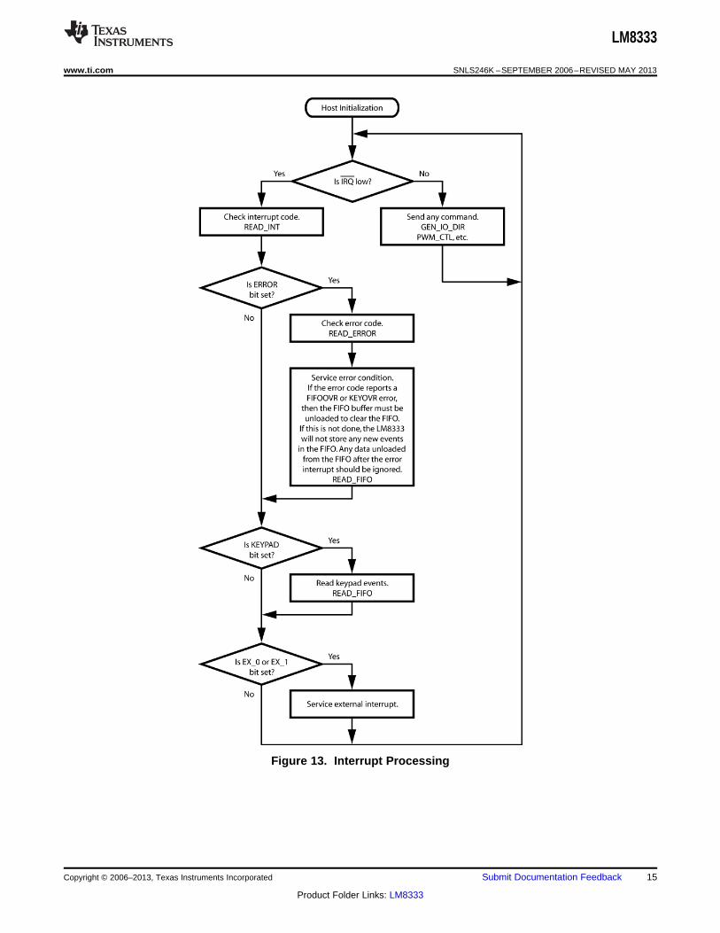
INTERRUPT PROCESSING
Unexpected states encountered during run-time, for example overrun of the FIFO buffer, are reported as errors.When the host receives an interrupt from the LM8333, it uses a READ_INT command to read the interrupt code.If the code has a set ERROR bit, the host then uses a READ_ERROR command to read the error code, asshown in Figure 13.
14 Submit Documentation Feedback Copyright © 2006–2013, Texas Instruments Incorporated
Product Folder Links: LM8333
LM8333
www.ti.com SNLS246K –SEPTEMBER 2006–REVISED MAY 2013
Figure 13. Interrupt Processing
Copyright © 2006–2013, Texas Instruments Incorporated Submit Documentation Feedback 15
Product Folder Links: LM8333

LM8333
SNLS246K –SEPTEMBER 2006–REVISED MAY 2013 www.ti.com
COMMAND EXECUTION SUMMARY• With the interrupt, status, and error codes, the LM8333 provides the features needed to support a reliable
key-scan functionality.• Up to 14 key-scan events can be stored in an internal FIFO buffer. The end of buffer is indicated with the 00
(empty character) code.• The host can repeatedly read the FIFO without modifying the FIFO pointer using the RPT_FIFO_READ
command (0x21), for example if an error is encountered during a read.• The LM8333 asserts the IRQ output low when a new character is pressed after the last interrupt acknowledge
from the host. The IRQ output will be deasserted after the host has acknowledged the interrupt by reading theinterrupt code using the READ_INT command (0xD0).
• The host can synchronize with the LM8333 by reading the status code with the READ_STAT command(0xE0). The status code verifies whether the last command was successfully completed.
• Two GPIO pins on the LM8333 may be configured as external interrupt inputs. A rising or falling edge on anenabled interrupt input triggers wake-up from Halt mode and asserts an interrupt to the host by pulling theIRQ output low.
• The host can change the debounce time from the default time of 10 ms. This can be used for reliablescanning of keyboards with noisy contacts. The debounce time can be set to about 1 second in steps of 4milliseconds. The debounce time is set with the DEBOUNCE command (0x22).
• The host can change the active time permitted before entering Halt mode from the default period of 500 ms.The active time is the time during which the keypad is scanned after the last key is released, before enteringHalt mode. The active time must be longer than the debounce time.
• The host can program the direction and output state of four general-purpose I/O pins. The host can also readthe states on these pins.
• The host can program a 16-bit timer for generating a PWM output. If the PWM function is not used, the PWMpin can be used as a general-purpose output.
16 Submit Documentation Feedback Copyright © 2006–2013, Texas Instruments Incorporated
Product Folder Links: LM8333

LM8333
www.ti.com SNLS246K –SEPTEMBER 2006–REVISED MAY 2013
These devices have limited built-in ESD protection. The leads should be shorted together or the device placed in conductive foamduring storage or handling to prevent electrostatic damage to the MOS gates.
ABSOLUTE MAXIMUM RATINGS (1) (2)
Supply Voltage (VCC) 3.5V
Voltage at Any Pin -0.3V to VCC +0.3V
Maximum Input Current Without Latchup ±100 mA
ESD Protection Level
Human Body Model 2 kV
Machine Model 200V
Total Current into VCC Pin (Source) 80 mA
Total Current out of GND Pin (Sink) 60 mA
Storage Temperature Range −65°C to +140°C
(1) Absolute Maximum Ratings indicate limits beyond which damage to the device may occur. Operating Ratings indicate conditions forwhich the device is intended to be functional, but specific performance is not specified. For specifications and test conditions, see theElectrical Characteristics tables.
(2) If Military/Aerospace specified devices are required, please contact the Texas Instruments Sales Office/ Distributors for availability andspecifications.
DC ELECTRICAL CHARACTERISTICS(Temperature: -40°C ≤ TA ≤ +85°C)Data sheet specification limits are specified by design, test, or statistical analysis.
Symbol Parameter Conditions Min (1) Typ Max (1) Units
VCC Operating Voltage 2.25 2.9 V
Power Supply Rise Time from 0.0V 20 µs 10 ms
(On Chip Power-On Reset Selected)
IDD Supply Current (2) RC Clock = 10 MHz, 6 mA
VCC = 2.75V, TC = 1 µs (3)
IHALT Standby Mode Current (4) VCC = 2.75V, TC = 0 µs, (3), TA <2 15 µA= 25°C
VIL Logical 0 Input Voltage 0.25 VCC V
VIH Logical 1 Input Voltage 0.8 VCC V
Hi-Z Input Leakage (TRI-STATE Output) VCC = 2.75V -0.1 0.1 µA
Input PullupCurrent VCC = 2.75V, VIN = 0V -15 -120 µA
Port Input Hysteresis (5) 0.1 V
Output Current Source (Weak Pull-Up) VCC = 2.25V, VOH = 1.7V -10 -80 µA
Output Current Source (Push-Pull Mode) VCC = 2.25V, VOH = 1.7V -10 mA
Output CurrentSink (Push-Pull Mode) VCC = 2.25V, VOL = 0.4V 10 mA
Allowable Sink and Source Current per Pin 16 mA
CPAD Input Capacitance 8.5 pF
(1) Data sheet minimum and maximum limits are specified by design, test, or statistical analysis.(2) Supply current is measured with inputs connected to VCC and outputs driven low but not connected to a load.(3) TC = instruction cycle time (min. 0.7 µs).(4) In Halt mode, the internal clock is switched off. Supply current in Halt mode is measured with inputs connected to VCC and outputs
driven low but not connected to a load.(5) Specified by design, not tested.
Copyright © 2006–2013, Texas Instruments Incorporated Submit Documentation Feedback 17
Product Folder Links: LM8333
LM8333
SNLS246K –SEPTEMBER 2006–REVISED MAY 2013 www.ti.com
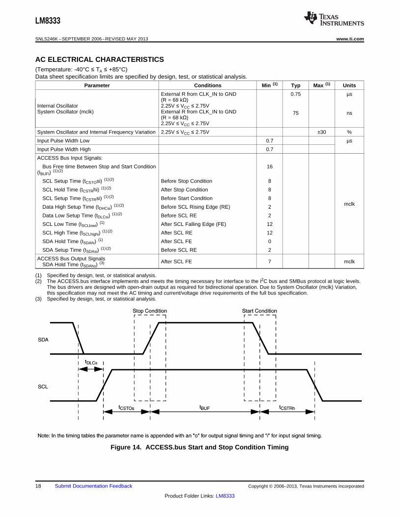
AC ELECTRICAL CHARACTERISTICS(Temperature: -40°C ≤ TA ≤ +85°C)Data sheet specification limits are specified by design, test, or statistical analysis.
Parameter Conditions Min (1) Typ Max (1) Units
External R from CLK_IN to GND 0.75 µs(R = 68 kΩ)
Internal Oscillator 2.25V ≤ VCC ≤ 2.75VSystem Oscillator (mclk) External R from CLK_IN to GND 75 ns
(R = 68 kΩ)2.25V ≤ VCC ≤ 2.75V
System Oscillator and Internal Frequency Variation 2.25V ≤ VCC ≤ 2.75V ±30 %
Input Pulse Width Low 0.7 µs
Input Pulse Width High 0.7
ACCESS Bus Input Signals:
Bus Free time Between Stop and Start Condition 16(IBUFI)
(1) (2)
SCL Setup Time (tCSTOsi) (1) (2) Before Stop Condition 8
SCL Hold Time (tCSTRhi) (1) (2) After Stop Condition 8
SCL Setup Time (tCSTRsi) (1) (2) Before Start Condition 8mclkData High Setup Time (tDHCsi)
(1) (2) Before SCL Rising Edge (RE) 2
Data Low Setup Time (tDLCsi)(1) (2) Before SCL RE 2
SCL Low Time (tSCLlowi)(1) After SCL Falling Edge (FE) 12
SCL High Time (tSCLhighi)(1) (2) After SCL RE 12
SDA Hold Time (tSDAhi)(1) After SCL FE 0
SDA Setup Time (tSDAsi)(1) (2) Before SCL RE 2
ACCESS Bus Output Signals After SCL FE 7 mclkSDA Hold Time (tSDAho) (3)
(1) Specified by design, test, or statistical analysis.(2) The ACCESS.bus interface implements and meets the timing necessary for interface to the I2C bus and SMBus protocol at logic levels.
The bus drivers are designed with open-drain output as required for bidirectional operation. Due to System Oscillator (mclk) Variation,this specification may not meet the AC timing and current/voltage drive requirements of the full bus specification.
(3) Specified by design, test, or statistical analysis.
Figure 14. ACCESS.bus Start and Stop Condition Timing
18 Submit Documentation Feedback Copyright © 2006–2013, Texas Instruments Incorporated
Product Folder Links: LM8333

LM8333
www.ti.com SNLS246K –SEPTEMBER 2006–REVISED MAY 2013
REVISION HISTORY
Changes from Revision J (May 2013) to Revision K Page
• Changed layout of National Data Sheet to TI format .......................................................................................................... 18
Copyright © 2006–2013, Texas Instruments Incorporated Submit Documentation Feedback 19
Product Folder Links: LM8333

PACKAGE OPTION ADDENDUM
www.ti.com 2-Oct-2017
Addendum-Page 1
PACKAGING INFORMATION
Orderable Device Status(1)
Package Type PackageDrawing
Pins PackageQty
Eco Plan(2)
Lead/Ball Finish(6)
MSL Peak Temp(3)
Op Temp (°C) Device Marking(4/5)
Samples
LM8333FLQ8X/NOPB ACTIVE WQFN NJE 32 2500 Green (RoHS& no Sb/Br)
CU SN Level-3-260C-168 HR -40 to 85 LM8333F
LM8333FLQ8Y/NOPB ACTIVE WQFN NJE 32 250 Green (RoHS& no Sb/Br)
CU SN Level-3-260C-168 HR -40 to 85 LM8333F
LM8333GGR8AXS/NOPB ACTIVE csBGA NYC 49 1000 Green (RoHS& no Sb/Br)
CU SNAGCU Level-1-260C-UNLIM -40 to 85 8333AXS
LM8333GGR8AXSX/NOPB ACTIVE csBGA NYC 49 3500 Green (RoHS& no Sb/Br)
CU SNAGCU Level-1-260C-UNLIM -40 to 85 8333AXS
(1) The marketing status values are defined as follows:ACTIVE: Product device recommended for new designs.LIFEBUY: TI has announced that the device will be discontinued, and a lifetime-buy period is in effect.NRND: Not recommended for new designs. Device is in production to support existing customers, but TI does not recommend using this part in a new design.PREVIEW: Device has been announced but is not in production. Samples may or may not be available.OBSOLETE: TI has discontinued the production of the device.
(2) RoHS: TI defines "RoHS" to mean semiconductor products that are compliant with the current EU RoHS requirements for all 10 RoHS substances, including the requirement that RoHS substancedo not exceed 0.1% by weight in homogeneous materials. Where designed to be soldered at high temperatures, "RoHS" products are suitable for use in specified lead-free processes. TI mayreference these types of products as "Pb-Free".RoHS Exempt: TI defines "RoHS Exempt" to mean products that contain lead but are compliant with EU RoHS pursuant to a specific EU RoHS exemption.Green: TI defines "Green" to mean the content of Chlorine (Cl) and Bromine (Br) based flame retardants meet JS709B low halogen requirements of <=1000ppm threshold. Antimony trioxide basedflame retardants must also meet the <=1000ppm threshold requirement.
(3) MSL, Peak Temp. - The Moisture Sensitivity Level rating according to the JEDEC industry standard classifications, and peak solder temperature.
(4) There may be additional marking, which relates to the logo, the lot trace code information, or the environmental category on the device.
(5) Multiple Device Markings will be inside parentheses. Only one Device Marking contained in parentheses and separated by a "~" will appear on a device. If a line is indented then it is a continuationof the previous line and the two combined represent the entire Device Marking for that device.
(6) Lead/Ball Finish - Orderable Devices may have multiple material finish options. Finish options are separated by a vertical ruled line. Lead/Ball Finish values may wrap to two lines if the finishvalue exceeds the maximum column width.
Important Information and Disclaimer:The information provided on this page represents TI's knowledge and belief as of the date that it is provided. TI bases its knowledge and belief on informationprovided by third parties, and makes no representation or warranty as to the accuracy of such information. Efforts are underway to better integrate information from third parties. TI has taken and

PACKAGE OPTION ADDENDUM
www.ti.com 2-Oct-2017
Addendum-Page 2
continues to take reasonable steps to provide representative and accurate information but may not have conducted destructive testing or chemical analysis on incoming materials and chemicals.TI and TI suppliers consider certain information to be proprietary, and thus CAS numbers and other limited information may not be available for release.
In no event shall TI's liability arising out of such information exceed the total purchase price of the TI part(s) at issue in this document sold by TI to Customer on an annual basis.

TAPE AND REEL INFORMATION
*All dimensions are nominal
Device PackageType
PackageDrawing
Pins SPQ ReelDiameter
(mm)
ReelWidth
W1 (mm)
A0(mm)
B0(mm)
K0(mm)
P1(mm)
W(mm)
Pin1Quadrant
LM8333FLQ8X/NOPB WQFN NJE 32 2500 330.0 16.4 6.3 6.3 1.5 12.0 16.0 Q1
LM8333FLQ8Y/NOPB WQFN NJE 32 250 178.0 16.4 6.3 6.3 1.5 12.0 16.0 Q1
LM8333GGR8AXS/NOPB csBGA NYC 49 1000 178.0 12.4 4.3 4.3 1.5 8.0 12.0 Q1
LM8333GGR8AXSX/NOPB
csBGA NYC 49 3500 330.0 12.4 4.3 4.3 1.5 8.0 12.0 Q1
PACKAGE MATERIALS INFORMATION
www.ti.com 24-Aug-2017
Pack Materials-Page 1

*All dimensions are nominal
Device Package Type Package Drawing Pins SPQ Length (mm) Width (mm) Height (mm)
LM8333FLQ8X/NOPB WQFN NJE 32 2500 367.0 367.0 38.0
LM8333FLQ8Y/NOPB WQFN NJE 32 250 210.0 185.0 35.0
LM8333GGR8AXS/NOPB csBGA NYC 49 1000 210.0 185.0 35.0
LM8333GGR8AXSX/NOPB csBGA NYC 49 3500 367.0 367.0 35.0
PACKAGE MATERIALS INFORMATION
www.ti.com 24-Aug-2017
Pack Materials-Page 2

MECHANICAL DATA
NYC0049A
www.ti.com
GRA49A (Rev A)

MECHANICAL DATA
NJE0032A
www.ti.com
LQA32A (REV A)

IMPORTANT NOTICE
Texas Instruments Incorporated (TI) reserves the right to make corrections, enhancements, improvements and other changes to itssemiconductor products and services per JESD46, latest issue, and to discontinue any product or service per JESD48, latest issue. Buyersshould obtain the latest relevant information before placing orders and should verify that such information is current and complete.TI’s published terms of sale for semiconductor products (http://www.ti.com/sc/docs/stdterms.htm) apply to the sale of packaged integratedcircuit products that TI has qualified and released to market. Additional terms may apply to the use or sale of other types of TI products andservices.Reproduction of significant portions of TI information in TI data sheets is permissible only if reproduction is without alteration and isaccompanied by all associated warranties, conditions, limitations, and notices. TI is not responsible or liable for such reproduceddocumentation. Information of third parties may be subject to additional restrictions. Resale of TI products or services with statementsdifferent from or beyond the parameters stated by TI for that product or service voids all express and any implied warranties for theassociated TI product or service and is an unfair and deceptive business practice. TI is not responsible or liable for any such statements.Buyers and others who are developing systems that incorporate TI products (collectively, “Designers”) understand and agree that Designersremain responsible for using their independent analysis, evaluation and judgment in designing their applications and that Designers havefull and exclusive responsibility to assure the safety of Designers' applications and compliance of their applications (and of all TI productsused in or for Designers’ applications) with all applicable regulations, laws and other applicable requirements. Designer represents that, withrespect to their applications, Designer has all the necessary expertise to create and implement safeguards that (1) anticipate dangerousconsequences of failures, (2) monitor failures and their consequences, and (3) lessen the likelihood of failures that might cause harm andtake appropriate actions. Designer agrees that prior to using or distributing any applications that include TI products, Designer willthoroughly test such applications and the functionality of such TI products as used in such applications.TI’s provision of technical, application or other design advice, quality characterization, reliability data or other services or information,including, but not limited to, reference designs and materials relating to evaluation modules, (collectively, “TI Resources”) are intended toassist designers who are developing applications that incorporate TI products; by downloading, accessing or using TI Resources in anyway, Designer (individually or, if Designer is acting on behalf of a company, Designer’s company) agrees to use any particular TI Resourcesolely for this purpose and subject to the terms of this Notice.TI’s provision of TI Resources does not expand or otherwise alter TI’s applicable published warranties or warranty disclaimers for TIproducts, and no additional obligations or liabilities arise from TI providing such TI Resources. TI reserves the right to make corrections,enhancements, improvements and other changes to its TI Resources. TI has not conducted any testing other than that specificallydescribed in the published documentation for a particular TI Resource.Designer is authorized to use, copy and modify any individual TI Resource only in connection with the development of applications thatinclude the TI product(s) identified in such TI Resource. NO OTHER LICENSE, EXPRESS OR IMPLIED, BY ESTOPPEL OR OTHERWISETO ANY OTHER TI INTELLECTUAL PROPERTY RIGHT, AND NO LICENSE TO ANY TECHNOLOGY OR INTELLECTUAL PROPERTYRIGHT OF TI OR ANY THIRD PARTY IS GRANTED HEREIN, including but not limited to any patent right, copyright, mask work right, orother intellectual property right relating to any combination, machine, or process in which TI products or services are used. Informationregarding or referencing third-party products or services does not constitute a license to use such products or services, or a warranty orendorsement thereof. Use of TI Resources may require a license from a third party under the patents or other intellectual property of thethird party, or a license from TI under the patents or other intellectual property of TI.TI RESOURCES ARE PROVIDED “AS IS” AND WITH ALL FAULTS. TI DISCLAIMS ALL OTHER WARRANTIES ORREPRESENTATIONS, EXPRESS OR IMPLIED, REGARDING RESOURCES OR USE THEREOF, INCLUDING BUT NOT LIMITED TOACCURACY OR COMPLETENESS, TITLE, ANY EPIDEMIC FAILURE WARRANTY AND ANY IMPLIED WARRANTIES OFMERCHANTABILITY, FITNESS FOR A PARTICULAR PURPOSE, AND NON-INFRINGEMENT OF ANY THIRD PARTY INTELLECTUALPROPERTY RIGHTS. TI SHALL NOT BE LIABLE FOR AND SHALL NOT DEFEND OR INDEMNIFY DESIGNER AGAINST ANY CLAIM,INCLUDING BUT NOT LIMITED TO ANY INFRINGEMENT CLAIM THAT RELATES TO OR IS BASED ON ANY COMBINATION OFPRODUCTS EVEN IF DESCRIBED IN TI RESOURCES OR OTHERWISE. IN NO EVENT SHALL TI BE LIABLE FOR ANY ACTUAL,DIRECT, SPECIAL, COLLATERAL, INDIRECT, PUNITIVE, INCIDENTAL, CONSEQUENTIAL OR EXEMPLARY DAMAGES INCONNECTION WITH OR ARISING OUT OF TI RESOURCES OR USE THEREOF, AND REGARDLESS OF WHETHER TI HAS BEENADVISED OF THE POSSIBILITY OF SUCH DAMAGES.Unless TI has explicitly designated an individual product as meeting the requirements of a particular industry standard (e.g., ISO/TS 16949and ISO 26262), TI is not responsible for any failure to meet such industry standard requirements.Where TI specifically promotes products as facilitating functional safety or as compliant with industry functional safety standards, suchproducts are intended to help enable customers to design and create their own applications that meet applicable functional safety standardsand requirements. Using products in an application does not by itself establish any safety features in the application. Designers mustensure compliance with safety-related requirements and standards applicable to their applications. Designer may not use any TI products inlife-critical medical equipment unless authorized officers of the parties have executed a special contract specifically governing such use.Life-critical medical equipment is medical equipment where failure of such equipment would cause serious bodily injury or death (e.g., lifesupport, pacemakers, defibrillators, heart pumps, neurostimulators, and implantables). Such equipment includes, without limitation, allmedical devices identified by the U.S. Food and Drug Administration as Class III devices and equivalent classifications outside the U.S.TI may expressly designate certain products as completing a particular qualification (e.g., Q100, Military Grade, or Enhanced Product).Designers agree that it has the necessary expertise to select the product with the appropriate qualification designation for their applicationsand that proper product selection is at Designers’ own risk. Designers are solely responsible for compliance with all legal and regulatoryrequirements in connection with such selection.Designer will fully indemnify TI and its representatives against any damages, costs, losses, and/or liabilities arising out of Designer’s non-compliance with the terms and provisions of this Notice.
Mailing Address: Texas Instruments, Post Office Box 655303, Dallas, Texas 75265Copyright © 2017, Texas Instruments Incorporated