Embed Size (px)
Citation preview
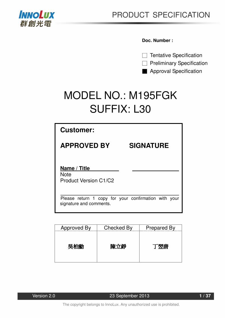
PRODUCT SPECIFICATION
Version 2.0 23 September 2013 1 / 37
The copyright belongs to InnoLux. Any unauthorized use is prohibited.
Customer: APPROVED BY SIGNATURE Name / Title Note Product Version C1/C2 Please return 1 copy for your confirmation with your signature and comments.
Doc. Number :
Tentative Specification Preliminary Specification Approval Specification
MODEL NO.: M195FGK SUFFIX: L30
Approved By Checked By Prepared By
PRODUCT SPECIFICATION
Version 2.0 23 September 2013 2 / 37
The copyright belongs to InnoLux. Any unauthorized use is prohibited.
CONTENTS
1. GENERAL DESCRIPTION.......................................................................................................5 1.1 OVERVIEW........................................................................................................................5 1.2 GENERAL SPECIFICATIONS ...........................................................................................5
2. MECHANICAL SPECIFICATIONS ...........................................................................................5 3. ABSOLUTE MAXIMUM RATINGS............................................................................................6
3.1 ABSOLUTE RATINGS OF ENVIRONMENT......................................................................6 3.2 ELECTRICAL ABSOLUTE RATINGS ................................................................................6
3.2.1 TFT-LCD MODULE .................................................................................................... 6 3.2.2 BACKLIGHT UNIT...................................................................................................... 7 3.2.3 Touch Module ............................................................................................................. 7
4. ELECTRICAL SPECIFICATIONS.............................................................................................7 4.1.1 FUNCTION BLOCK DIAGRAM .................................................................................. 7 4.1.2 TOUCH FUNCTION BLOCK DIAGRAM..................................................................... 7
4.2. INTERFACE CONNECTIONS ..........................................................................................8 4.2.1 Module LCD PIN ASSIGNMENT ................................................................................ 8 4.2.2 Module Panel Connector Information ......................................................................... 8 4.2.3 Touch Sensor PIN ASSIGNMENT .............................................................................. 9 4.2.4 Touch Sensor Connector Information ......................................................................... 9
4.3 ELECTRICAL CHARACTERISTICS ................................................................................10 4.3.1 LCD ELETRONICS SPECIFICATION ...................................................................... 10 4.3.2 Vcc Power Dip Condition.......................................................................................... 12 4.3.3 BACKLIGHT UNIT.................................................................................................... 12 4.3.4 LIGHTBAR Connector Pin Assignment .................................................................... 14
4.4 LVDS INPUT SIGNAL SPECIFICATIONS........................................................................15 4.4.1 LVDS DATA MAPPING TABLE ................................................................................. 15 4.4.2 COLOR DATA INPUT ASSIGNMENT....................................................................... 16
4.5 DISPLAY TIMING SPECIFICATIONS ..............................................................................17 5.TOUCH SENSOR SPECIFICATION .......................................................................................20
5.1 TOUCH GENERAL SPECIFICATION ..............................................................................20 5.2 TOUCH ELECTRICAL SPECIFICATION .........................................................................21 5.3 TOUCH TEST CONDITIONS...........................................................................................21
6. OPTICAL CHARACTERISTICS .............................................................................................21 6.1 TEST CONDITIONS ........................................................................................................21 6.2 OPTICAL SPECIFICATIONS ...........................................................................................21
7. RELIABILITY TEST ITEM.......................................................................................................24
PRODUCT SPECIFICATION
Version 2.0 23 September 2013 3 / 37
The copyright belongs to InnoLux. Any unauthorized use is prohibited.
8. MECHANICAL STRENGTH CHARACTERISTICS.................................................................25 8.1 MECHANICAL STRENGTH CHARACTERISTICS ..........................................................25 8.2 TEST CONDITIONS ........................................................................................................25 8.3 DEFINITION OF TEST POINTS ......................................................................................25
9.PACKING ................................................................................................................................26 9.1 PACKING SPECIFICATIONS ..........................................................................................26 9.2 PACKING METHOD.........................................................................................................27 9.2 PALLET............................................................................................................................28 9.3 UN-PACKING METHOD ..................................................................................................29
10. INX MODULE LABEL...........................................................................................................30 11. PRECAUTIONS....................................................................................................................31
11.1 ASSEMBLY AND HANDLING PRECAUTIONS..............................................................31 11.2 STORAGE PRECAUTIONS...........................................................................................31 11.3 OPERATION PRECAUTIONS........................................................................................31 11.4 SAFETY PRECAUTIONS ..............................................................................................32 11.5 SAFETY STANDARDS ..................................................................................................32 11.6 OTHER...........................................................................................................................32
Appendix 1. SYSTEM COVER DESIGN NOTICE......................................................................32 Appendix 2. OUTLINE DRAWING..............................................................................................35
PRODUCT SPECIFICATION
Version 2.0 23 September 2013 4 / 37
The copyright belongs to InnoLux. Any unauthorized use is prohibited.
REVISION HISTORY
Version Date Page Description
2.0 2013.Aug.10 Approval spec was first issued.
PRODUCT SPECIFICATION
Version 2.0 23 September 2013 5 / 37
The copyright belongs to InnoLux. Any unauthorized use is prohibited.
1. GENERAL DESCRIPTION
1.1 OVERVIEW M195FGK-L30 is a 19.5” TFT Liquid Crystal Display module with PCT* sensor embedded, white-LED
back-light unit and 30 pins 2 channels LVDS interface. This module supports 1600x900 native resolutions
and can display up to 16.7 millions colors. The converter module for Backlight is not built in.
*Projected Capacitive Touch
1.2 GENERAL SPECIFICATIONS Item Specification Unit Note
Active Area Size 19.5” real diagonal
Driver Element a-si TFT active matrix -
Pixel Number 1600 x R.G.B. x 900 pixel
Pixel Pitch 0.27 (H) x 0.27 (V) mm
Pixel Arrangement RGB vertical stripe -
Display Colors 16.7M color
Transmissive Mode Normally white -
Luminance, White 200 nits cd/m2
Color Gamut 72% of NTSC(Typ.) -
Touch Technology Projected Capacitive Multi-Touch Panel -
Touch Method Finger or Electrically Charged Object -
Numbers of Touch 10 Points
Interface USB -
Cover Glass Type EXG -
RoHS,Halogen Free &TCO 5.2 RoHS, Halogen Free compliance -
Power Consumption Total (14.87W) @ cell (4.7W), BL (9.72W), Touch sensor (450mW) (1)
Note (1) The specified power consumption: Total= cell(reference 4.3.1)+BL(reference 4.3.3)+TP(reference)
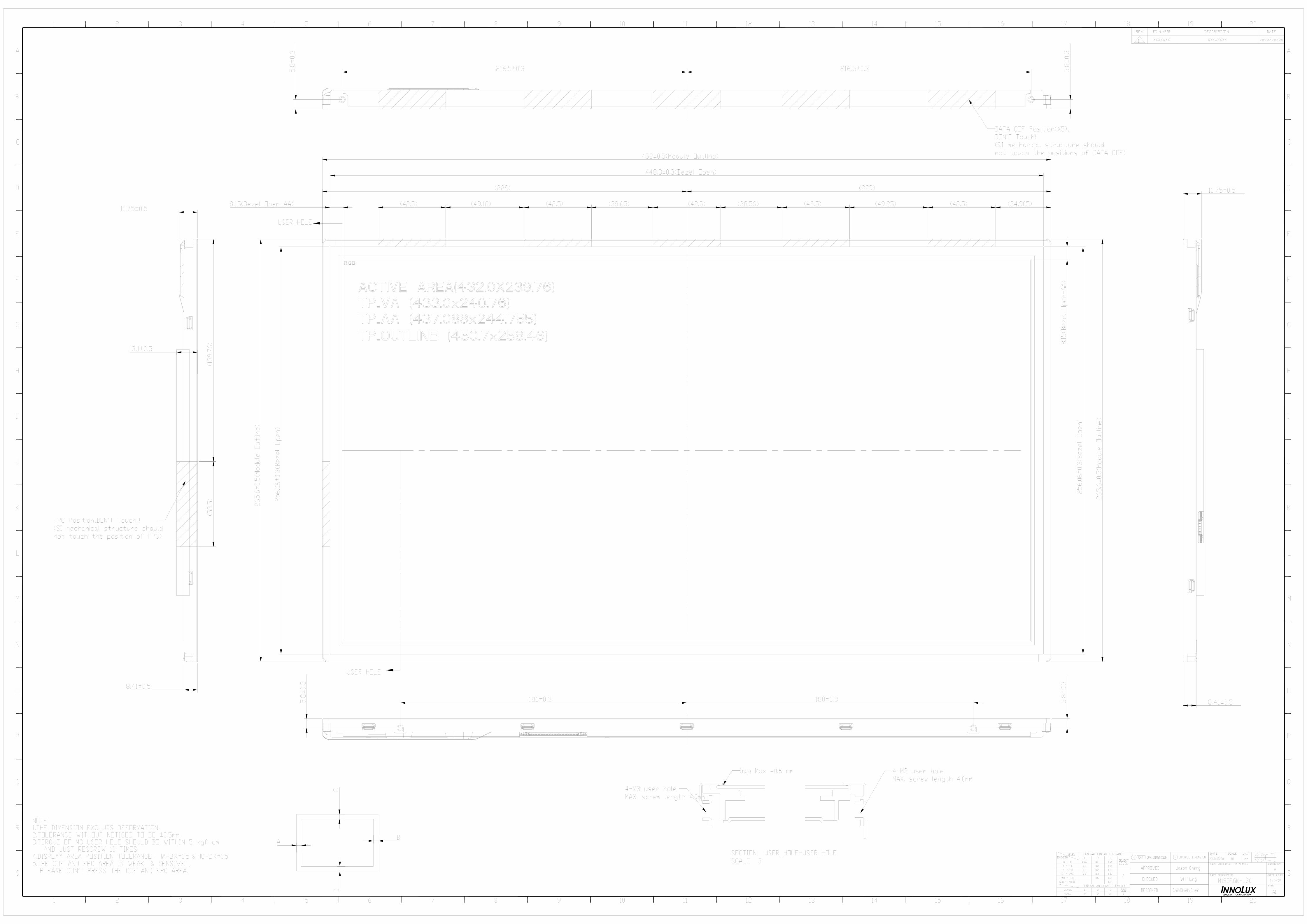
2. MECHANICAL SPECIFICATIONS
Item Min. Typ. Max. Unit Note
Horizontal 457.5 458 458.5 mm
Vertical 265.1 265.6 266.1 mm Module Size
Thickness - 13.1 13.6 mm
(1)
Horizontal 448.0 448.3 448.6 mm Bezel Area
Vertical 255.76 256.06 256.36 mm
Horizontal 433.0 mm Touch Sensor Visible Area Vertical 240.76 mm
Horizontal - 432.0 - Display Active Area Vertical - 239.76 - mm
Weight 1580 1650 g
Note (1) Please refer to the attached drawings for more information of front and back outline dimensions.
PRODUCT SPECIFICATION
Version 2.0 23 September 2013 6 / 37
The copyright belongs to InnoLux. Any unauthorized use is prohibited.
3. ABSOLUTE MAXIMUM RATINGS
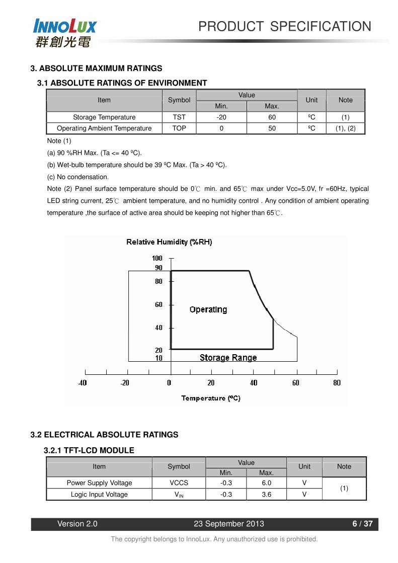
3.1 ABSOLUTE RATINGS OF ENVIRONMENT Value
Item Symbol Min. Max.
Unit Note
Storage Temperature TST -20 60 ºC (1)
Operating Ambient Temperature TOP 0 50 ºC (1), (2)
Note (1)
(a) 90 %RH Max. (Ta <= 40 ºC).
(b) Wet-bulb temperature should be 39 ºC Max. (Ta > 40 ºC).
(c) No condensation.
Note (2) Panel surface temperature should be 0 min. and 65 max under Vcc=5.0V, fr =60Hz, typical
LED string current, 25 ambient temperature, and no humidity control . Any condition of ambient operating
temperature ,the surface of active area should be keeping not higher than 65.
3.2 ELECTRICAL ABSOLUTE RATINGS
3.2.1 TFT-LCD MODULE Value Item Symbol
Min. Max. Unit Note
Power Supply Voltage VCCS -0.3 6.0 V
Logic Input Voltage VIN -0.3 3.6 V (1)
PRODUCT SPECIFICATION
Version 2.0 23 September 2013 7 / 37
The copyright belongs to InnoLux. Any unauthorized use is prohibited.
3.2.2 BACKLIGHT UNIT Value Item Symbol
Min. Typ Max. Unit Note
LED Forward Current Per Input Pin IF 0 65 69 mA (1), (2)
Duty=100%
LED Pulse Forward Current Per Input Pin IP --- --- 200 mA
(1), (2) Pulse Width10msec.
and Duty10%
Note (1) Permanent damage to the device may occur if maximum values are exceeded. Function operation
should be restricted to the conditions described under Normal Operating Conditions.
Note (2) Specified values are for input pin of LED light bar at Ta=25±2 (Refer to 4.3.3 and 4.3.4 for
further information).
3.2.3 Touch Module Value Item Symbol
Min. Max. Unit Note
DC Supply Voltage USB_VDD -0.5 6.0 V
4. ELECTRICAL SPECIFICATIONS
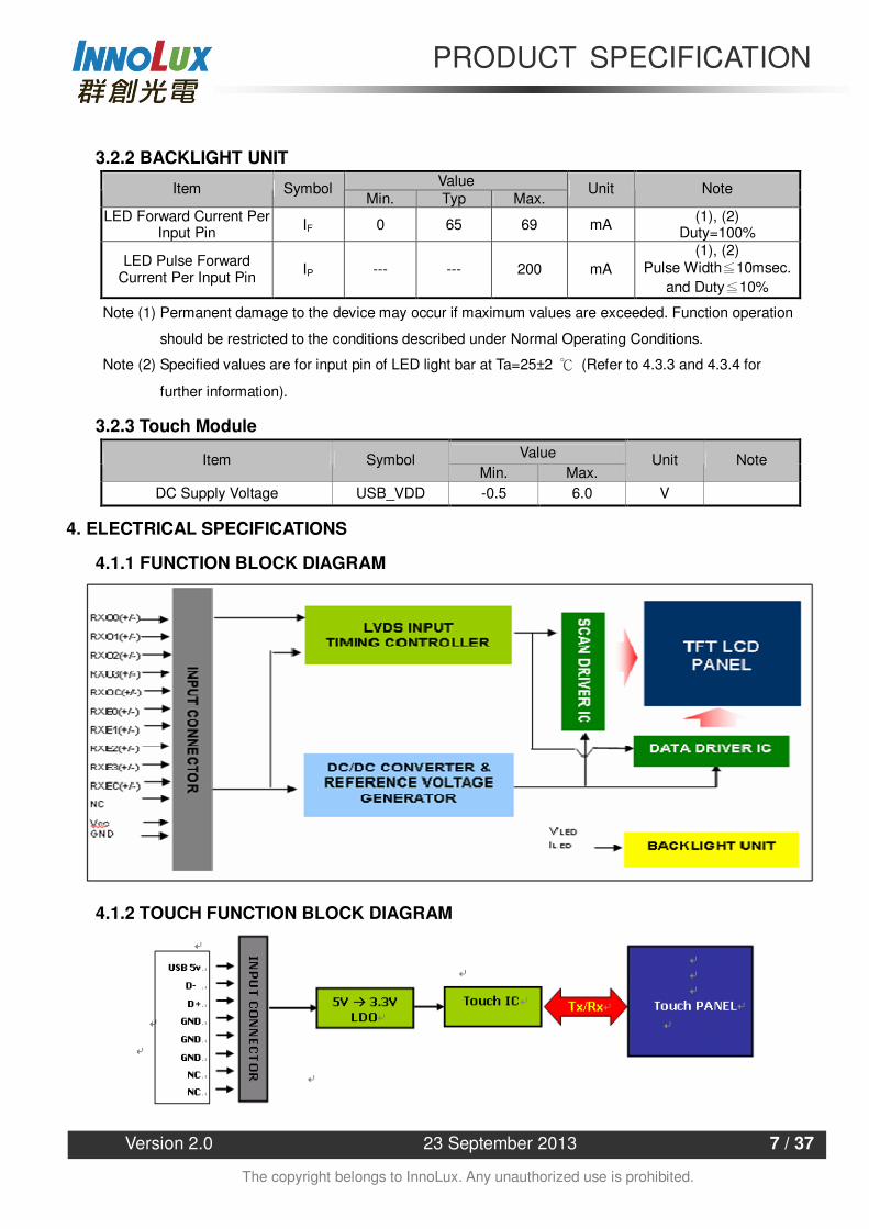
4.1.1 FUNCTION BLOCK DIAGRAM
4.1.2 TOUCH FUNCTION BLOCK DIAGRAM
PRODUCT SPECIFICATION
Version 2.0 23 September 2013 8 / 37
The copyright belongs to InnoLux. Any unauthorized use is prohibited.
4.2. INTERFACE CONNECTIONS
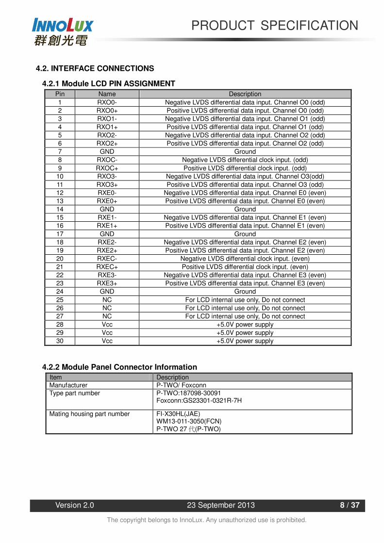
4.2.1 Module LCD PIN ASSIGNMENT Pin Name Description 1 RXO0- Negative LVDS differential data input. Channel O0 (odd) 2 RXO0+ Positive LVDS differential data input. Channel O0 (odd) 3 RXO1- Negative LVDS differential data input. Channel O1 (odd) 4 RXO1+ Positive LVDS differential data input. Channel O1 (odd) 5 RXO2- Negative LVDS differential data input. Channel O2 (odd) 6 RXO2+ Positive LVDS differential data input. Channel O2 (odd) 7 GND Ground 8 RXOC- Negative LVDS differential clock input. (odd) 9 RXOC+ Positive LVDS differential clock input. (odd)
10 RXO3- Negative LVDS differential data input. Channel O3(odd) 11 RXO3+ Positive LVDS differential data input. Channel O3 (odd) 12 RXE0- Negative LVDS differential data input. Channel E0 (even) 13 RXE0+ Positive LVDS differential data input. Channel E0 (even) 14 GND Ground 15 RXE1- Negative LVDS differential data input. Channel E1 (even) 16 RXE1+ Positive LVDS differential data input. Channel E1 (even) 17 GND Ground 18 RXE2- Negative LVDS differential data input. Channel E2 (even) 19 RXE2+ Positive LVDS differential data input. Channel E2 (even) 20 RXEC- Negative LVDS differential clock input. (even) 21 RXEC+ Positive LVDS differential clock input. (even) 22 RXE3- Negative LVDS differential data input. Channel E3 (even) 23 RXE3+ Positive LVDS differential data input. Channel E3 (even) 24 GND Ground 25 NC For LCD internal use only, Do not connect 26 NC For LCD internal use only, Do not connect 27 NC For LCD internal use only, Do not connect 28 Vcc +5.0V power supply 29 Vcc +5.0V power supply 30 Vcc +5.0V power supply
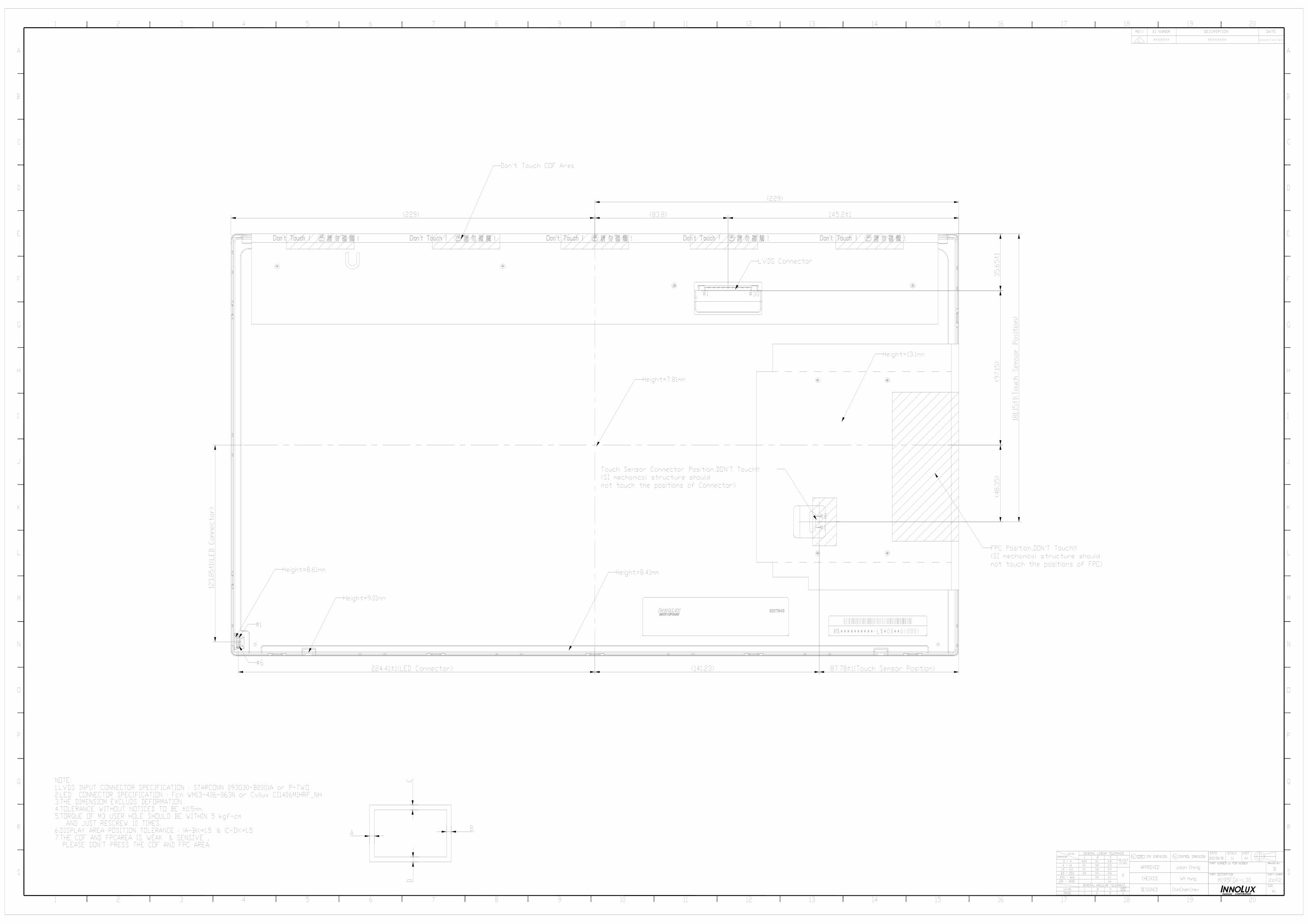
4.2.2 Module Panel Connector Information Item Description Manufacturer P-TWO/ Foxconn Type part number P-TWO:187098-30091
Foxconn:GS23301-0321R-7H
Mating housing part number FI-X30HL(JAE) WM13-011-3050(FCN) P-TWO 27 (P-TWO)
PRODUCT SPECIFICATION
Version 2.0 23 September 2013 9 / 37
The copyright belongs to InnoLux. Any unauthorized use is prohibited.
4.2.3 Touch Sensor PIN ASSIGNMENT Pin Name Description 1 USB_VDD USB power 2 D- USB D- 3 D+ USB D+ 4 GND USB ground 5 GND USB ground 6 GND USB ground 7 NC No Connection 8 NC No Connection
4.2.4 Touch Sensor Connector Information Item Description Manufacturer FCN Type part number FCN WM13-406-083N Mating housing part number WF1300106-B
*Notice: There would be compatible issues, if not using the indicated connectors in the matching list.
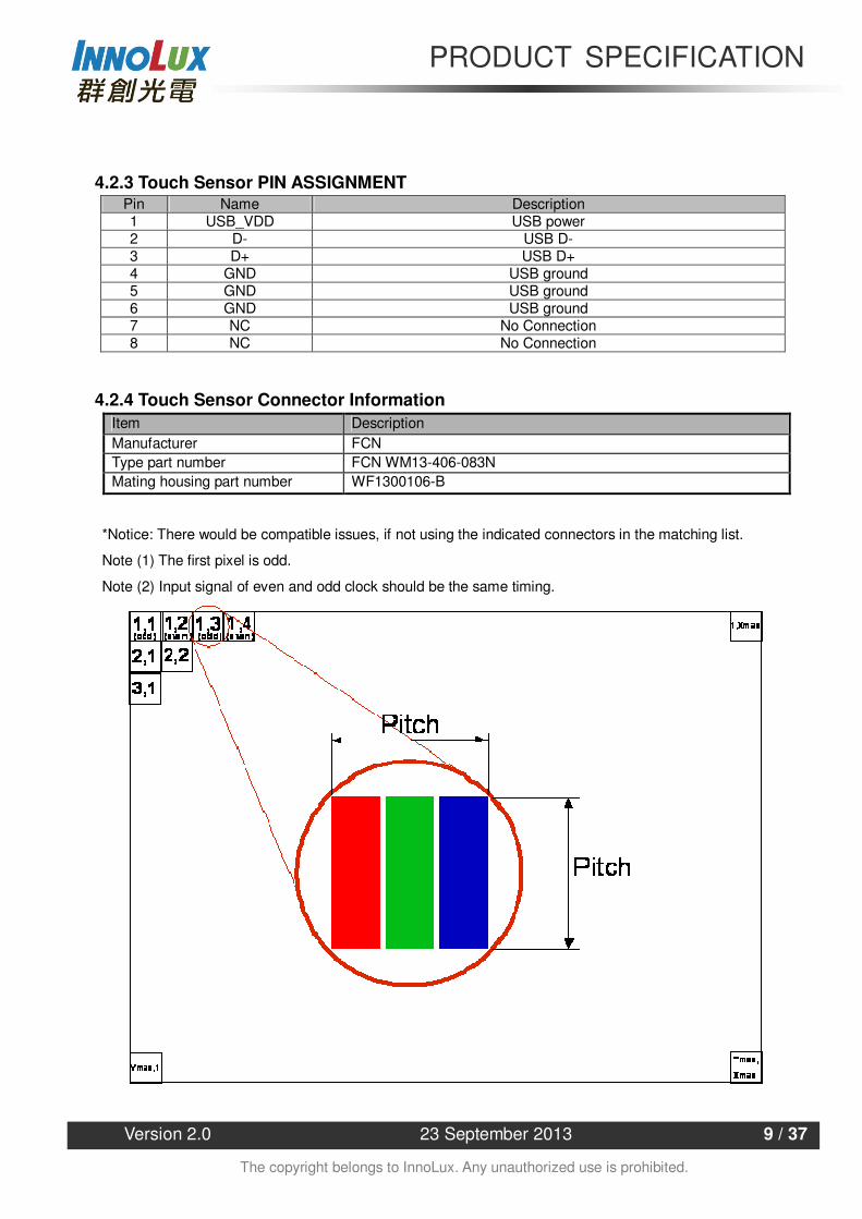
Note (1) The first pixel is odd.
Note (2) Input signal of even and odd clock should be the same timing.
PRODUCT SPECIFICATION
Version 2.0 23 September 2013 10 / 37
The copyright belongs to InnoLux. Any unauthorized use is prohibited.
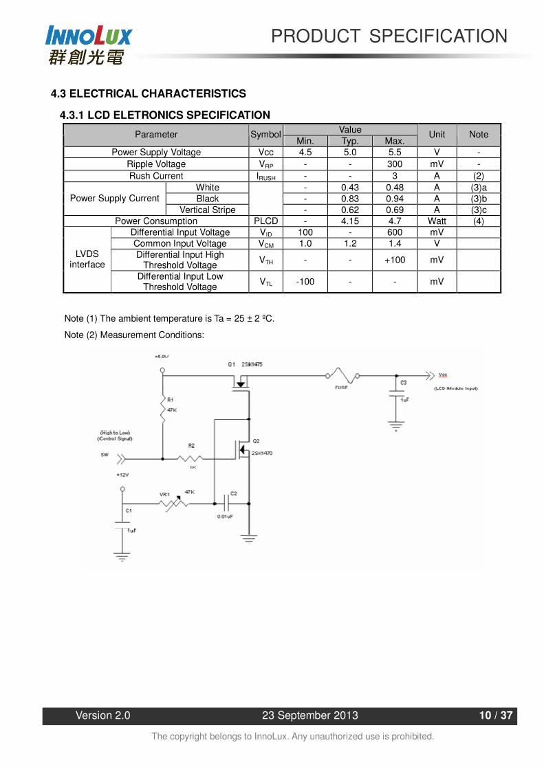
4.3 ELECTRICAL CHARACTERISTICS
4.3.1 LCD ELETRONICS SPECIFICATION Value Parameter Symbol
Min. Typ. Max. Unit Note
Power Supply Voltage Vcc 4.5 5.0 5.5 V - Ripple Voltage VRP - - 300 mV - Rush Current IRUSH - - 3 A (2)
White - 0.43 0.48 A (3)a Black - 0.83 0.94 A (3)b Power Supply Current
Vertical Stripe
- 0.62 0.69 A (3)c Power Consumption PLCD - 4.15 4.7 Watt (4)
Differential Input Voltage VID 100 - 600 mV Common Input Voltage VCM 1.0 1.2 1.4 V Differential Input High
Threshold Voltage VTH - - +100 mV LVDS
interface Differential Input Low
Threshold Voltage VTL -100 - - mV
Note (1) The ambient temperature is Ta = 25 ± 2 ºC.
Note (2) Measurement Conditions:
PRODUCT SPECIFICATION
Version 2.0 23 September 2013 11 / 37
The copyright belongs to InnoLux. Any unauthorized use is prohibited.
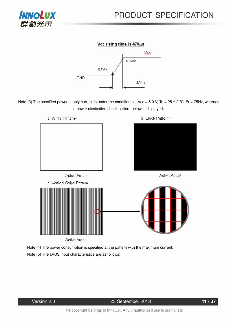
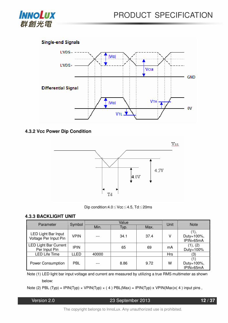
Note (3) The specified power supply current is under the conditions at Vcc = 5.0 V, Ta = 25 ± 2 ºC, Fr = 75Hz, whereas
a power dissipation check pattern below is displayed.
Note (4) The power consumption is specified at the pattern with the maximum current.
Note (5) The LVDS input characteristics are as follows:
PRODUCT SPECIFICATION
Version 2.0 23 September 2013 12 / 37
The copyright belongs to InnoLux. Any unauthorized use is prohibited.
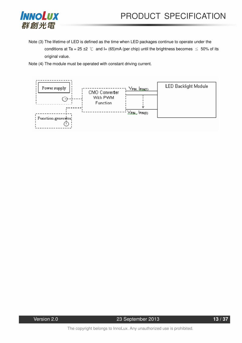
4.3.2 Vcc Power Dip Condition
Dip condition:4.0Vcc4.5, Td20ms
4.3.3 BACKLIGHT UNIT Value Parameter Symbol
Min. Typ. Max. Unit Note
LED Light Bar Input Voltage Per Input Pin VPIN --- 34.1 37.4 V
(1), Duty=100%, IPIN=65mA
LED Light Bar Current Per Input Pin IPIN 65 69 mA (1), (2)
Duty=100% LED Life Time LLED 40000 Hrs (3)
Power Consumption PBL --- 8.86 9.72 W (1)
Duty=100%, IPIN=65mA
Note (1) LED light bar input voltage and current are measured by utilizing a true RMS multimeter as shown
below:
Note (2) PBL (Typ) = IPIN(Typ) × VPIN(Typ) × ( 4 ) PBL(Max) = IPIN(Typ) x VPIN(Max)x( 4 ) input pins ,
PRODUCT SPECIFICATION
Version 2.0 23 September 2013 13 / 37
The copyright belongs to InnoLux. Any unauthorized use is prohibited.
Note (3) The lifetime of LED is defined as the time when LED packages continue to operate under the
conditions at Ta = 25 ±2 and I= (65)mA (per chip) until the brightness becomes 50% of its
original value.
Note (4) The module must be operated with constant driving current.
PRODUCT SPECIFICATION
Version 2.0 23 September 2013 14 / 37
The copyright belongs to InnoLux. Any unauthorized use is prohibited.
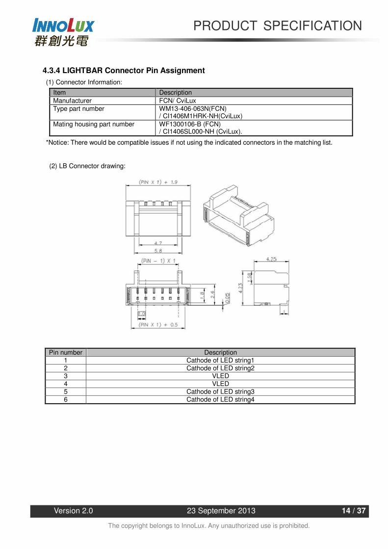
4.3.4 LIGHTBAR Connector Pin Assignment (1) Connector Information:
Item Description Manufacturer FCN/ CviLux Type part number WM13-406-063N(FCN)
/ CI1406M1HRK-NH(CviLux) Mating housing part number WF1300106-B (FCN)
/ CI1406SL000-NH (CviLux).
*Notice: There would be compatible issues if not using the indicated connectors in the matching list.
(2) LB Connector drawing:
Pin number Description 1 Cathode of LED string1 2 Cathode of LED string2 3 VLED 4 VLED 5 Cathode of LED string3 6 Cathode of LED string4
PRODUCT SPECIFICATION
Version 2.0 23 September 2013 15 / 37
The copyright belongs to InnoLux. Any unauthorized use is prohibited.
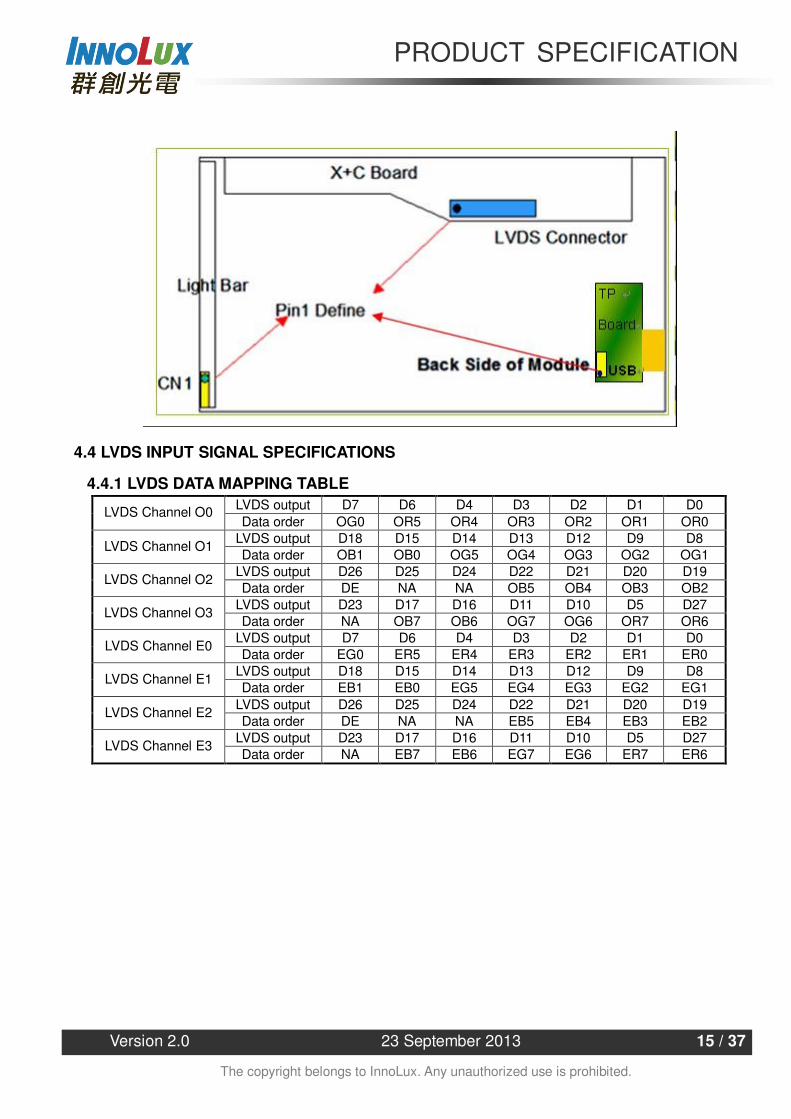
4.4 LVDS INPUT SIGNAL SPECIFICATIONS
4.4.1 LVDS DATA MAPPING TABLE LVDS output D7 D6 D4 D3 D2 D1 D0 LVDS Channel O0 Data order OG0 OR5 OR4 OR3 OR2 OR1 OR0
LVDS output D18 D15 D14 D13 D12 D9 D8 LVDS Channel O1 Data order OB1 OB0 OG5 OG4 OG3 OG2 OG1
LVDS output D26 D25 D24 D22 D21 D20 D19 LVDS Channel O2 Data order DE NA NA OB5 OB4 OB3 OB2
LVDS output D23 D17 D16 D11 D10 D5 D27 LVDS Channel O3 Data order NA OB7 OB6 OG7 OG6 OR7 OR6
LVDS output D7 D6 D4 D3 D2 D1 D0 LVDS Channel E0 Data order EG0 ER5 ER4 ER3 ER2 ER1 ER0
LVDS output D18 D15 D14 D13 D12 D9 D8 LVDS Channel E1 Data order EB1 EB0 EG5 EG4 EG3 EG2 EG1
LVDS output D26 D25 D24 D22 D21 D20 D19 LVDS Channel E2 Data order DE NA NA EB5 EB4 EB3 EB2
LVDS output D23 D17 D16 D11 D10 D5 D27 LVDS Channel E3 Data order NA EB7 EB6 EG7 EG6 ER7 ER6
PRODUCT SPECIFICATION
Version 2.0 23 September 2013 16 / 37
The copyright belongs to InnoLux. Any unauthorized use is prohibited.
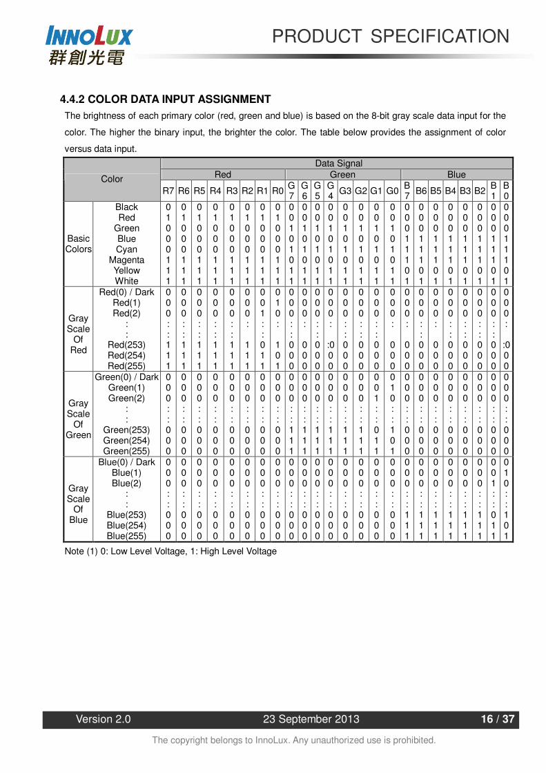
4.4.2 COLOR DATA INPUT ASSIGNMENT The brightness of each primary color (red, green and blue) is based on the 8-bit gray scale data input for the
color. The higher the binary input, the brighter the color. The table below provides the assignment of color
versus data input.
Data Signal Red Green Blue Color
R7 R6 R5 R4 R3 R2 R1 R0 G7
G6
G5
G4 G3 G2 G1 G0 B
7 B6 B5 B4 B3 B2 B1
B0
Basic Colors
Black Red
Green Blue Cyan
Magenta Yellow White
0 1 0 0 0 1 1 1
0 1 0 0 0 1 1 1
0 1 0 0 0 1 1 1
0 1 0 0 0 1 1 1
0 1 0 0 0 1 1 1
0 1 0 0 0 1 1 1
0 1 0 0 0 1 1 1
0 1 0 0 0 1 1 1
0 0 1 0 1 0 1 1
0 0 1 0 1 0 1 1
0 0 1 0 1 0 1 1
0 0 1 0 1 0 1 1
0 0 1 0 1 0 1 1
0 0 1 0 1 0 1 1
0 0 1 0 1 0 1 1
0 0 1 0 1 0 1 1
0 0 0 1 1 1 0 1
0 0 0 1 1 1 0 1
0 0 0 1 1 1 0 1
0 0 0 1 1 1 0 1
0 0 0 1 1 1 0 1
0 0 0 1 1 1 0 1
0 0 0 1 1 1 0 1
0 0 0 1 1 1 0 1
Gray Scale
Of Red
Red(0) / Dark Red(1) Red(2)
: :
Red(253) Red(254) Red(255)
0 0 0 : : 1 1 1
0 0 0 : : 1 1 1
0 0 0 : : 1 1 1
0 0 0 : : 1 1 1
0 0 0 : : 1 1 1
0 0 0 :
1 1 1
0 0 1 : : 0 1 1
0 1 0 :
1 0 1
0 0 0 : : 0 0 0
0 0 0 :
0 0 0
0 0 0 : : 0 0 0
0 0 0 :
:0 0 0
0 0 0 : : 0 0 0
0 0 0 : : 0 0 0
0 0 0 : : 0 0 0
0 0 0 :
0 0 0
0 0 0 :
0 0 0
0 0 0 : : 0 0 0
0 0 0 :
0 0 0
0 0 0 : : 0 0 0
0 0 0 : : 0 0 0
0 0 0 : : 0 0 0
0 0 0 : : 0 0 0
0 0 0 :
:0 0 0
Gray Scale
Of Green
Green(0) / Dark Green(1) Green(2)
: :
Green(253) Green(254) Green(255)
0 0 0 : : 0 0 0
0 0 0 : : 0 0 0
0 0 0 : : 0 0 0
0 0 0 : : 0 0 0
0 0 0 : : 0 0 0
0 0 0 : : 0 0 0
0 0 0 : : 0 0 0
0 0 0 : : 0 0 0
0 0 0 : : 1 1 1
0 0 0 : : 1 1 1
0 0 0 : : 1 1 1
0 0 0 : : 1 1 1
0 0 0 : : 1 1 1
0 0 0 : : 1 1 1
0 0 1 : : 0 1 1
0 1 0 : : 1 0 1
0 0 0 : : 0 0 0
0 0 0 : : 0 0 0
0 0 0 : : 0 0 0
0 0 0 : : 0 0 0
0 0 0 : : 0 0 0
0 0 0 : : 0 0 0
0 0 0 : : 0 0 0
0 0 0 : : 0 0 0
Gray Scale
Of Blue
Blue(0) / Dark Blue(1) Blue(2)
: :
Blue(253) Blue(254) Blue(255)
0 0 0 : : 0 0 0
0 0 0 : : 0 0 0
0 0 0 : : 0 0 0
0 0 0 : : 0 0 0
0 0 0 : : 0 0 0
0 0 0 : : 0 0 0
0 0 0 : : 0 0 0
0 0 0 : : 0 0 0
0 0 0 : : 0 0 0
0 0 0 : : 0 0 0
0 0 0 : : 0 0 0
0 0 0 : : 0 0 0
0 0 0 : : 0 0 0
0 0 0 : : 0 0 0
0 0 0 : : 0 0 0
0 0 0 : : 0 0 0
0 0 0 : : 1 1 1
0 0 0 : : 1 1 1
0 0 0 : : 1 1 1
0 0 0 : : 1 1 1
0 0 0 : : 1 1 1
0 0 0 : : 1 1 1
0 0 1 : : 0 1 1
0 1 0 : : 1 0 1
Note (1) 0: Low Level Voltage, 1: High Level Voltage
PRODUCT SPECIFICATION
Version 2.0 23 September 2013 17 / 37
The copyright belongs to InnoLux. Any unauthorized use is prohibited.
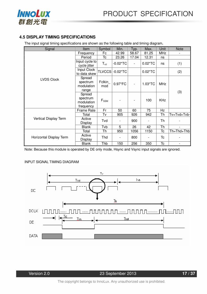
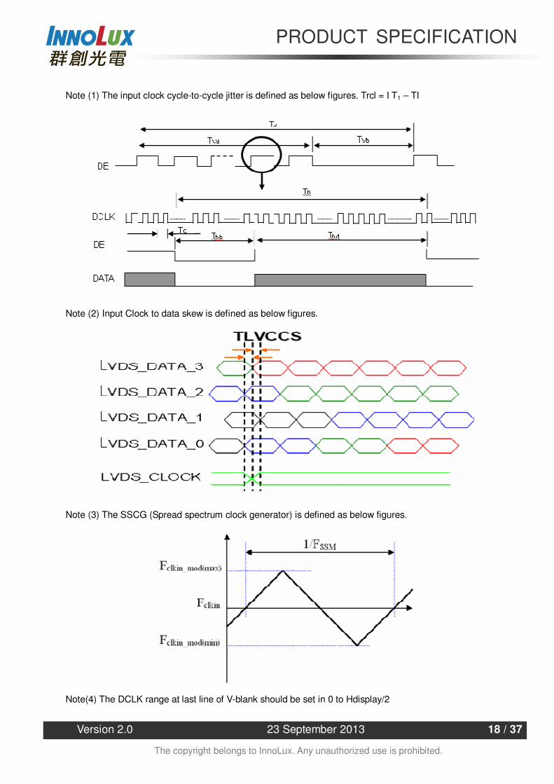
4.5 DISPLAY TIMING SPECIFICATIONS The input signal timing specifications are shown as the following table and timing diagram.
Signal Item Symbol Min. Typ. Max. Unit Note Frequency Fc 42.99 58.67 81.25 MHz -
Period Tc 23.26 17.04 12.31 ns Input cycle to
cycle jitter Trcl -0.02*TC - 0.02*TC ns (1)
Input Clock to data skew TLVCCS -0.02*TC 0.02*TC (2)
Spread spectrum
modulation range
Fclkin_mod
0.97*FC - 1.03*TC MHz LVDS Clock
Spread spectrum
modulation frequency
FSSM - - 100 KHz
(3)
Frame Rate Fr 50 60 75 Hz Total Tv 905 926 942 Th Tv=Tvd+Tvb-
Active Display Tvd - 900 - Th -
Vertical Display Term
Blank Tvb 5 26 42 Th - Total Th 950 1056 1150 Tc Th=Thd+Thb
Active Display Thd - 800 - Tc - Horizontal Display Term
Blank Thb 150 256 350 Tc -
Note: Because this module is operated by DE only mode, Hsync and Vsync input signals are ignored.
INPUT SIGNAL TIMING DIAGRAM
PRODUCT SPECIFICATION
Version 2.0 23 September 2013 18 / 37
The copyright belongs to InnoLux. Any unauthorized use is prohibited.
Note (1) The input clock cycle-to-cycle jitter is defined as below figures. Trcl = I T1 – TI
Note (2) Input Clock to data skew is defined as below figures.
Note (3) The SSCG (Spread spectrum clock generator) is defined as below figures.
Note(4) The DCLK range at last line of V-blank should be set in 0 to Hdisplay/2
PRODUCT SPECIFICATION
Version 2.0 23 September 2013 19 / 37
The copyright belongs to InnoLux. Any unauthorized use is prohibited.
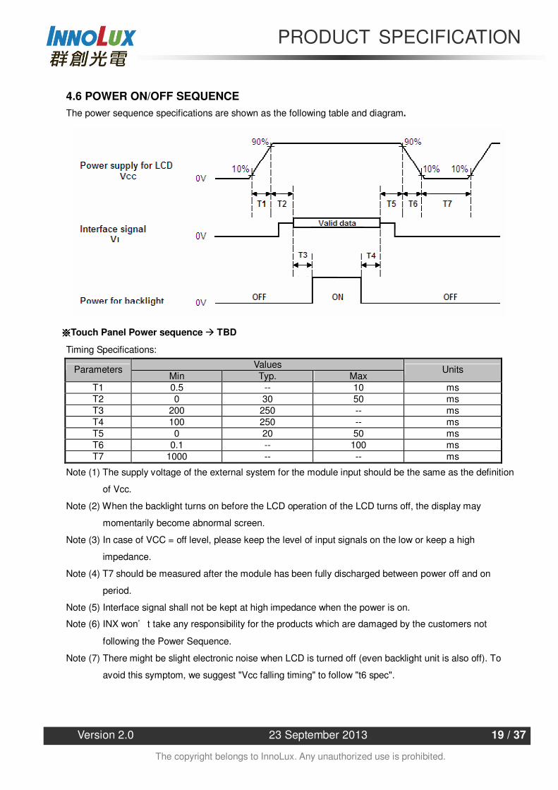
4.6 POWER ON/OFF SEQUENCE The power sequence specifications are shown as the following table and diagram.
Touch Panel Power sequence TBD
Timing Specifications:
Values Parameters Min Typ. Max
Units
T1 0.5 -- 10 ms T2 0 30 50 ms T3 200 250 -- ms T4 100 250 -- ms T5 0 20 50 ms T6 0.1 -- 100 ms T7 1000 -- -- ms
Note (1) The supply voltage of the external system for the module input should be the same as the definition
of Vcc.
Note (2) When the backlight turns on before the LCD operation of the LCD turns off, the display may
momentarily become abnormal screen.
Note (3) In case of VCC = off level, please keep the level of input signals on the low or keep a high
impedance.
Note (4) T7 should be measured after the module has been fully discharged between power off and on
period.
Note (5) Interface signal shall not be kept at high impedance when the power is on.
Note (6) INX wont take any responsibility for the products which are damaged by the customers not
following the Power Sequence.
Note (7) There might be slight electronic noise when LCD is turned off (even backlight unit is also off). To
avoid this symptom, we suggest "Vcc falling timing" to follow "t6 spec".
PRODUCT SPECIFICATION
Version 2.0 23 September 2013 20 / 37
The copyright belongs to InnoLux. Any unauthorized use is prohibited.
5.TOUCH SENSOR SPECIFICATION
5.1 TOUCH GENERAL SPECIFICATION Items General
Touch Module Size 19.5”
Touch Technology Projected Capacitive Multi-Touch Panel
Number of Channels 87*49
Touch Method Finger
Numbers of Touch 10 Points
Accuracy +/- 1 mm
Linearity Maximum of 1 mm over 10 mm of travel
Reporting rate >100 Hz
Minimum stylus diameter 9 mm
Sensor Glass Material EXG Glass
TP unit cell pattern pitch size X 5024um/Y4995um
TP Type One Glass Sensor ( Sensor on Lens)
Touch Module Outline 458 * 265.6 mm
Touch Active Area 437.088 * 244.755 mm
Touch Window Visible Area 433.0 * 240.76 mm
Touch Panel Thickness 0.52 mm +/-0.1 (WIS 0.5mm & Ink 0.2mm)
Surface Hardness 6H
Items Electrical
Supply Voltage USB: 5V
Interface USB
Touch Channels (X - Y) 87*49
Sensor Pitch (X - Y) X 5024um/Y4995um
PRODUCT SPECIFICATION
Version 2.0 23 September 2013 21 / 37
The copyright belongs to InnoLux. Any unauthorized use is prohibited.
5.2 TOUCH ELECTRICAL SPECIFICATION Value Item Symbol
Min. Typ. Max. Unit Note
USB Power Supply Voltage USB 4.8 5 5.2 V
Active mode IDD 120 mA
Idle mode IDD TBD mA Power Consumption
Sleep mode IDD 0 mA
5.3 TOUCH TEST CONDITIONS All of the touch test conditions are following Win 8 specification.
6. OPTICAL CHARACTERISTICS
6.1 TEST CONDITIONS Item Symbol Value Unit
Ambient Temperature Ta 25±2 oC Ambient Humidity Ha 50±10 %RH
Supply Voltage VCC 5 V Input Signal According to typical value in "3. ELECTRICAL CHARACTERISTICS"
LED Light Bar Input Current Per Input Pin IPIN 65 ± 1.95 mADC
PWM Duty Ratio D 100 % LED Light Bar Test Converter INX 27-D041745
6.2 OPTICAL SPECIFICATIONS The relative measurement methods of optical characteristics are shown in 5.2. The following items should be
measured under the test conditions described in 5.1 and stable environment shown in Note (5).
Item Symbol Condition Min. Typ. Max. Unit Note Rx 0.636
Red Ry 0.338 Gx 0.311 Green Gy 0.629 Bx 0.159
Blue By 0.065 Wx 0.313
Color Chromaticity (CIE 1931)
White Wy
Typ – 0.03
0.329
Typ + 0.03 - (1), (5)
Center Luminance of White (Center of Screen) LC 150 200 - cd/m2 (4), (5)
Contrast Ratio CR
θx=0°, θY =0° CS-2000
R=G=B=255 Gray scale
700 1000 - - (2), (5) TR - 1.5 2.5 Response Time TF θx=0°, θY =0° - 3.5 5.5
ms (3)
White Variation W θx=0°, θY =0° 75 - - % (5), (6) Horizontal θx- + θx+ 150 170 -
Viewing Angle Vertical θy- + θy+
CR 10 140 160 -
Deg. (1), (5)
Horizontal θx- + θx+ 160 178 --- Viewing Angle
Vertical θy- + θy+ CR 5
150 170 --- Deg. (1), (5)
PRODUCT SPECIFICATION
Version 2.0 23 September 2013 22 / 37
The copyright belongs to InnoLux. Any unauthorized use is prohibited.
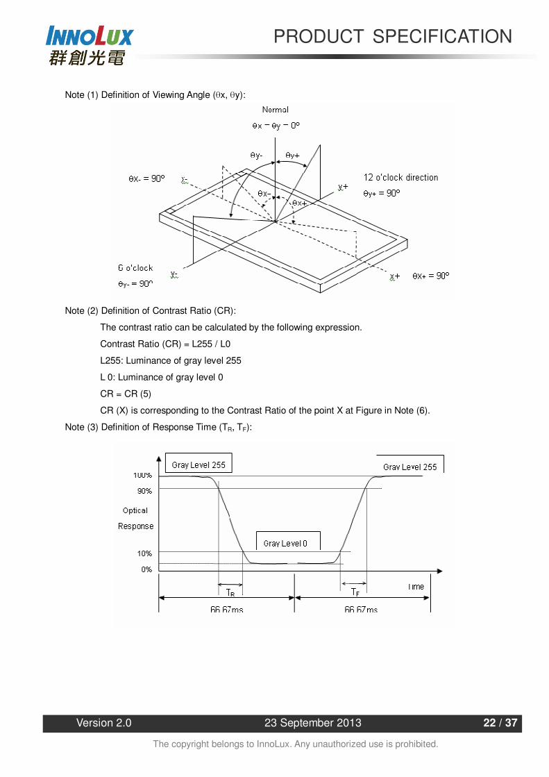
Note (1) Definition of Viewing Angle (θx, θy):
Note (2) Definition of Contrast Ratio (CR):
The contrast ratio can be calculated by the following expression.
Contrast Ratio (CR) = L255 / L0
L255: Luminance of gray level 255
L 0: Luminance of gray level 0
CR = CR (5)
CR (X) is corresponding to the Contrast Ratio of the point X at Figure in Note (6).
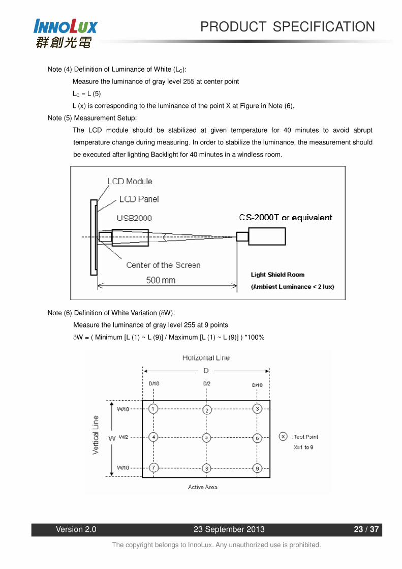
Note (3) Definition of Response Time (TR, TF):
PRODUCT SPECIFICATION
Version 2.0 23 September 2013 23 / 37
The copyright belongs to InnoLux. Any unauthorized use is prohibited.
Note (4) Definition of Luminance of White (LC):
Measure the luminance of gray level 255 at center point
LC = L (5)
L (x) is corresponding to the luminance of the point X at Figure in Note (6).
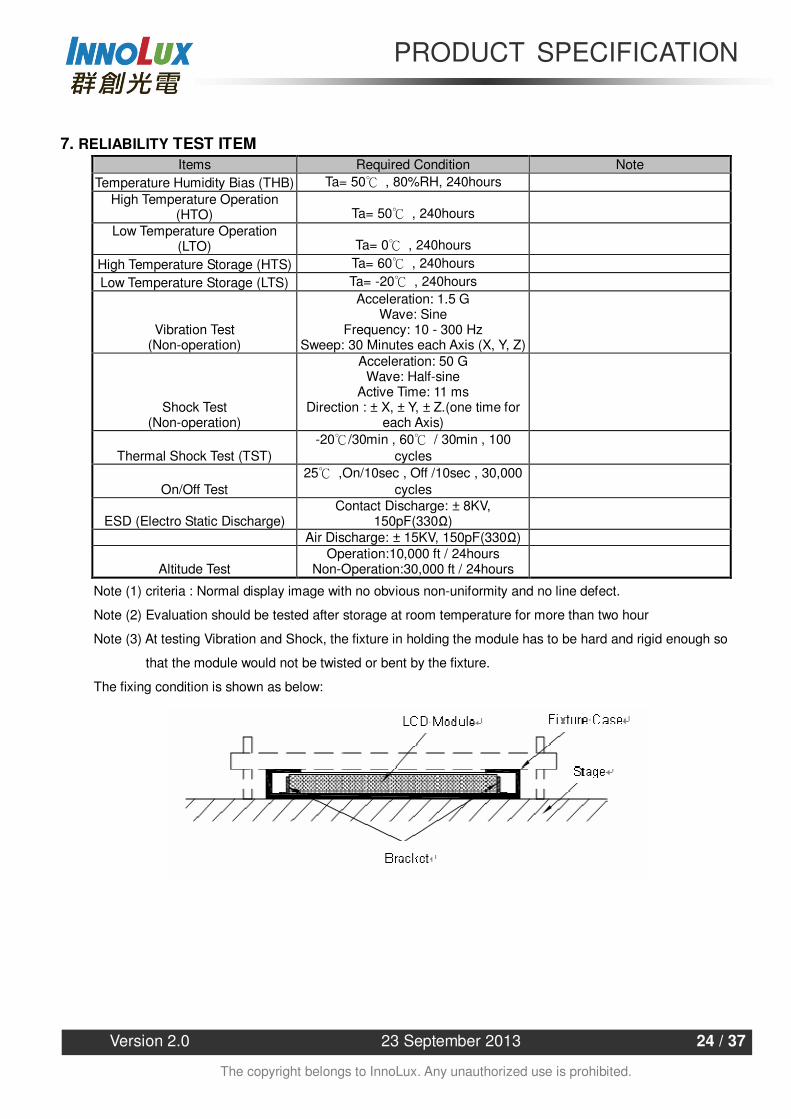
Note (5) Measurement Setup:
The LCD module should be stabilized at given temperature for 40 minutes to avoid abrupt
temperature change during measuring. In order to stabilize the luminance, the measurement should
be executed after lighting Backlight for 40 minutes in a windless room.
Note (6) Definition of White Variation (δW):
Measure the luminance of gray level 255 at 9 points
δW = ( Minimum [L (1) ~ L (9)] / Maximum [L (1) ~ L (9)] ) *100%
PRODUCT SPECIFICATION
Version 2.0 23 September 2013 24 / 37
The copyright belongs to InnoLux. Any unauthorized use is prohibited.
7. RELIABILITY TEST ITEM Items Required Condition Note
Temperature Humidity Bias (THB) Ta= 50 , 80%RH, 240hours High Temperature Operation
(HTO) Ta= 50 , 240hours
Low Temperature Operation (LTO) Ta= 0 , 240hours
High Temperature Storage (HTS) Ta= 60 , 240hours Low Temperature Storage (LTS) Ta= -20 , 240hours
Vibration Test (Non-operation)
Acceleration: 1.5 G Wave: Sine
Frequency: 10 - 300 Hz Sweep: 30 Minutes each Axis (X, Y, Z)
Shock Test (Non-operation)
Acceleration: 50 G Wave: Half-sine
Active Time: 11 ms Direction : ± X, ± Y, ± Z.(one time for
each Axis)
Thermal Shock Test (TST) -20/30min , 60 / 30min , 100
cycles
On/Off Test 25 ,On/10sec , Off /10sec , 30,000
cycles
ESD (Electro Static Discharge) Contact Discharge: ± 8KV,
150pF(330Ω)
Air Discharge: ± 15KV, 150pF(330Ω)
Altitude Test Operation:10,000 ft / 24hours
Non-Operation:30,000 ft / 24hours
Note (1) criteria : Normal display image with no obvious non-uniformity and no line defect.
Note (2) Evaluation should be tested after storage at room temperature for more than two hour
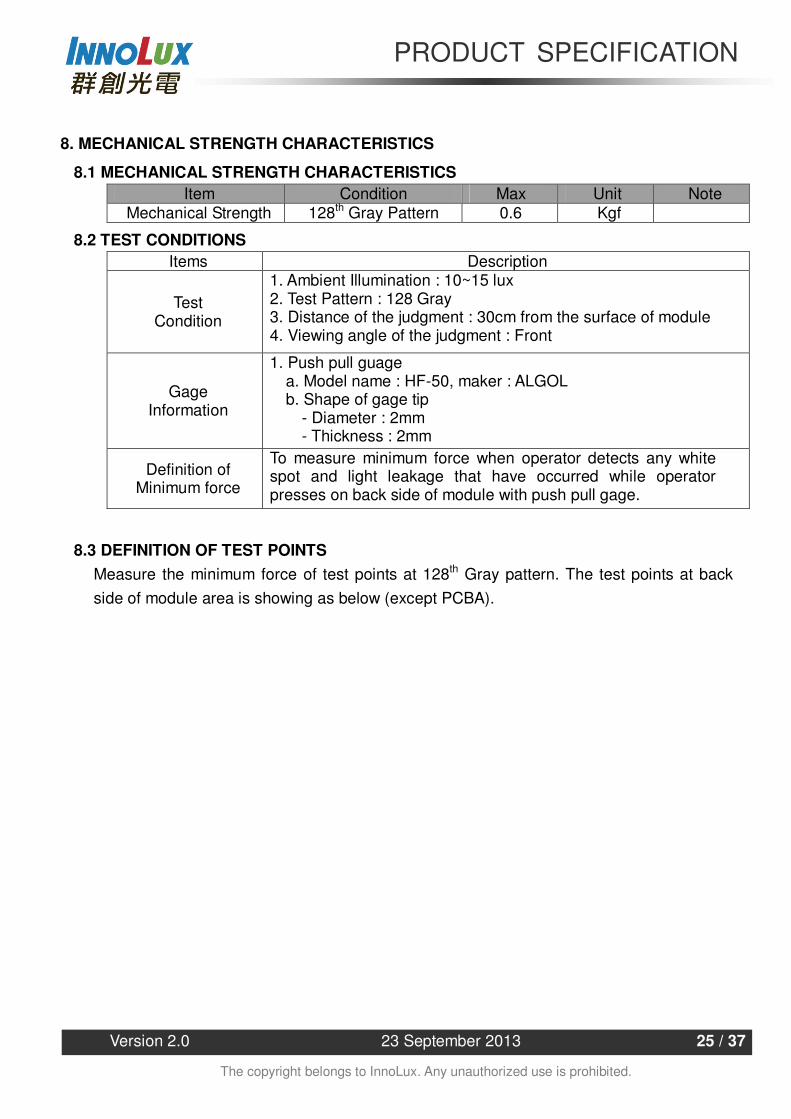
Note (3) At testing Vibration and Shock, the fixture in holding the module has to be hard and rigid enough so
that the module would not be twisted or bent by the fixture.
The fixing condition is shown as below:
PRODUCT SPECIFICATION
Version 2.0 23 September 2013 25 / 37
The copyright belongs to InnoLux. Any unauthorized use is prohibited.
8. MECHANICAL STRENGTH CHARACTERISTICS
8.1 MECHANICAL STRENGTH CHARACTERISTICS Item Condition Max Unit Note
Mechanical Strength 128th Gray Pattern 0.6 Kgf
8.2 TEST CONDITIONS Items Description
Test Condition
1. Ambient Illumination : 10~15 lux 2. Test Pattern : 128 Gray 3. Distance of the judgment : 30cm from the surface of module 4. Viewing angle of the judgment : Front
Gage Information
1. Push pull guage a. Model name : HF-50, maker : ALGOL b. Shape of gage tip - Diameter : 2mm - Thickness : 2mm
Definition of Minimum force
To measure minimum force when operator detects any white spot and light leakage that have occurred while operator presses on back side of module with push pull gage.
8.3 DEFINITION OF TEST POINTS Measure the minimum force of test points at 128th Gray pattern. The test points at back side of module area is showing as below (except PCBA).
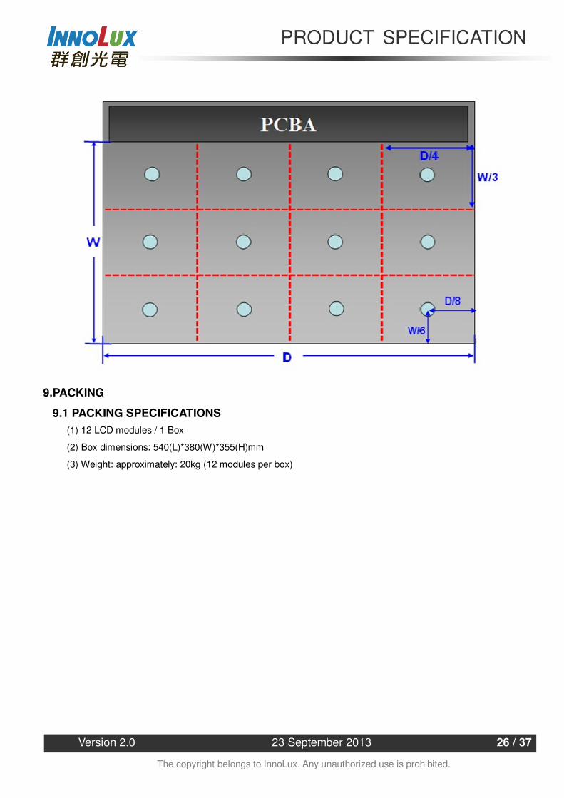
PRODUCT SPECIFICATION
Version 2.0 23 September 2013 26 / 37
The copyright belongs to InnoLux. Any unauthorized use is prohibited.
9.PACKING
9.1 PACKING SPECIFICATIONS (1) 12 LCD modules / 1 Box
(2) Box dimensions: 540(L)*380(W)*355(H)mm
(3) Weight: approximately: 20kg (12 modules per box)
PRODUCT SPECIFICATION
Version 2.0 23 September 2013 27 / 37
The copyright belongs to InnoLux. Any unauthorized use is prohibited.
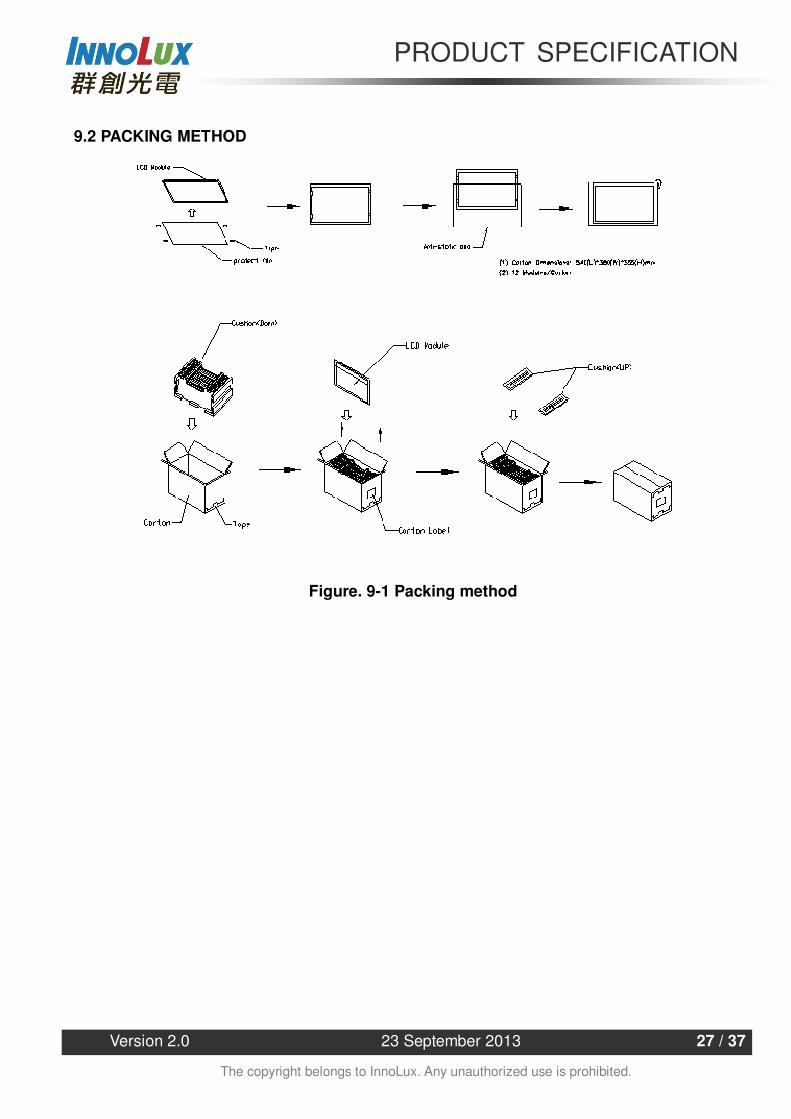
9.2 PACKING METHOD
Figure. 9-1 Packing method
PRODUCT SPECIFICATION
Version 2.0 23 September 2013 28 / 37
The copyright belongs to InnoLux. Any unauthorized use is prohibited.
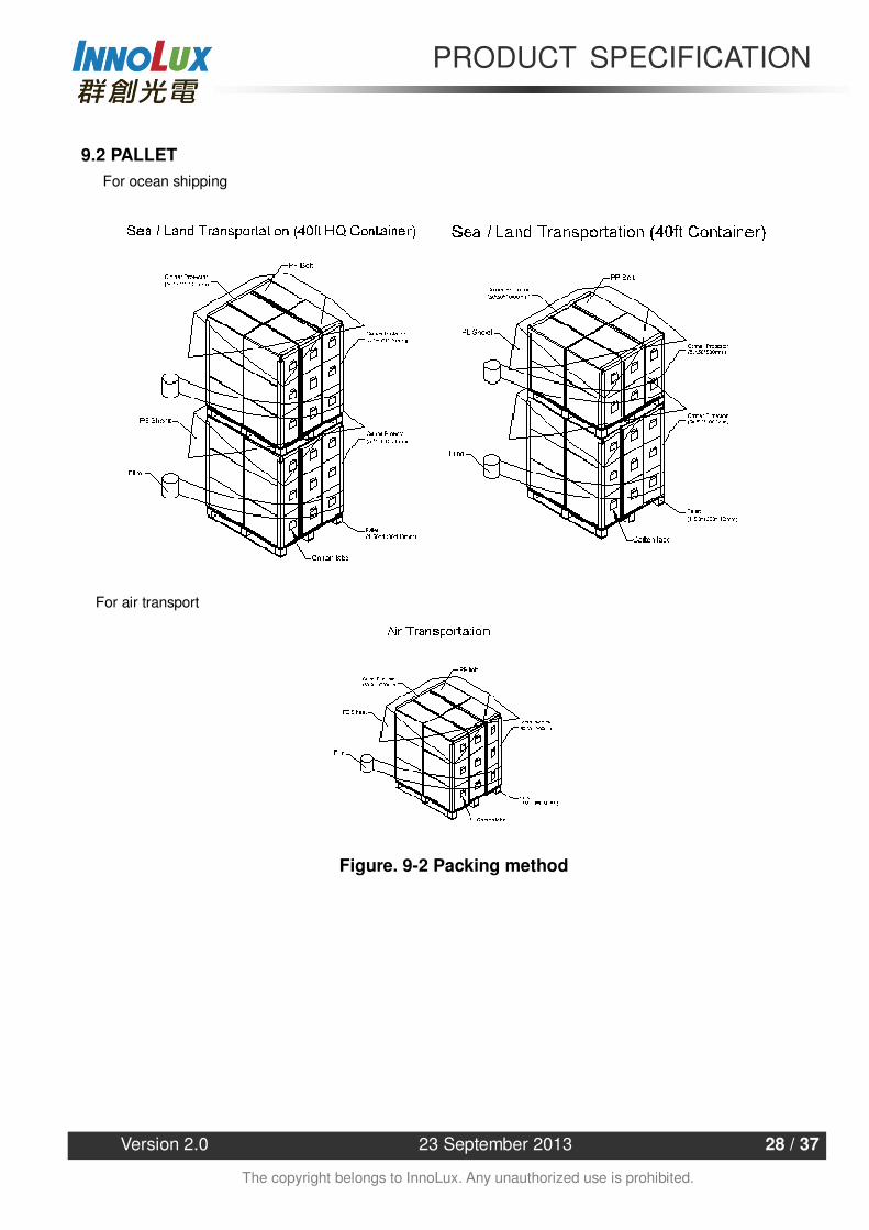
9.2 PALLET For ocean shipping
For air transport
Figure. 9-2 Packing method
PRODUCT SPECIFICATION
Version 2.0 23 September 2013 29 / 37
The copyright belongs to InnoLux. Any unauthorized use is prohibited.
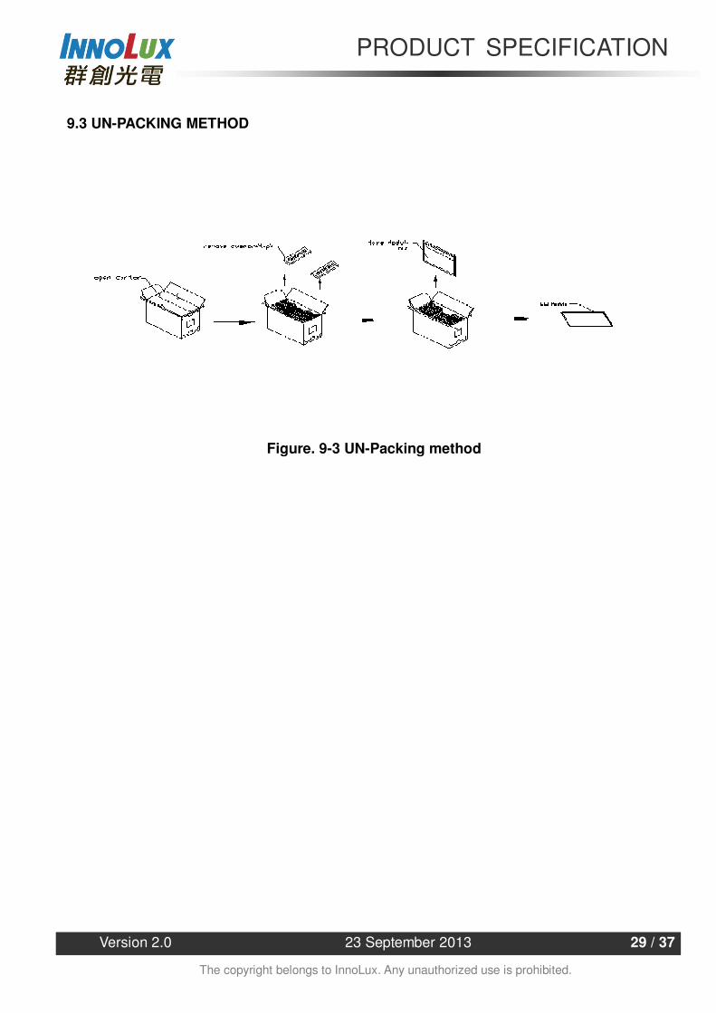
9.3 UN-PACKING METHOD
Figure. 9-3 UN-Packing method
PRODUCT SPECIFICATION
Version 2.0 23 September 2013 30 / 37
The copyright belongs to InnoLux. Any unauthorized use is prohibited.
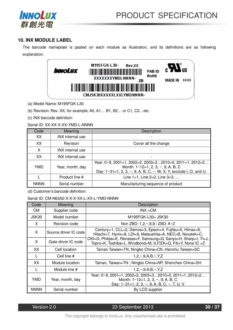
10. INX MODULE LABEL The barcode nameplate is pasted on each module as illustration, and its definitions are as following
explanation.
(a) Model Name: M195FGK-L30
(b) Revision: Rev. XX, for example: A0, A1… B1, B2… or C1, C2…etc.
(c) INX barcode definition:
Serial ID: XX-XX-X-XX-YMD-L-NNNN
Code Meaning Description XX INX internal use -
XX Revision Cover all the change
X INX internal use -
XX INX internal use -
YMD Year, month, day Year: 0~9, 2001=1, 2002=2, 2003=3…2010=0, 2011=1, 2012=2…
Month: 1~12=1, 2, 3, ~, 9, A, B, C Day: 1~31=1, 2, 3, ~, 9, A, B, C, ~, W, X, Y, exclude I, O, and U.
L Product line # Line 1=1, Line 2=2, Line 3=3, …
NNNN Serial number Manufacturing sequence of product
(d) Customer’s barcode definition:
Serial ID: CM-N63A2-X-X-X-XX-L-XX-L-YMD-NNNN
Code Meaning Description CM Supplier code INX =CM
J5K30 Model number M195FGK-L30= J5K30
X Revision code Non ZBD: 1,2,~,8,9 / ZBD: A~Z
X Source driver IC code
X Gate driver IC code
Century=1, CLL=2, Demos=3, Epson=4, Fujitsu=5, Himax=6, Hitachi=7, Hynix=8, LDI=9, Matsushita=A, NEC=B, Novatek=C,
OKI=D, Philips=E, Renasas=F, Samsung=G, Sanyo=H, Sharp=I, TI=J, Topro=K, Toshiba=L, Windbond=M, ILITEK=Q, Fiti=Y, None IC =Z
XX Cell location Tainan Taiwan=TN, Ningbo China=CN, Hsinchu Taiwan=SC
L Cell line # 1,2,~,9,A,B,~,Y,Z
XX Module location Tainan, Taiwan=TN ; Ningbo China=NP, Shenzhen China=SH
L Module line # 1,2,~,9,A,B,~,Y,Z
YMD Year, month, day Year: 0~9, 2001=1, 2002=2, 2003=3…2010=0, 2011=1, 2012=2…
Month: 1~12=1, 2, 3, ~, 9, A, B, C Day: 1~31=1, 2, 3, ~, 9, A, B, C, ~, T, U, V
NNNN Serial number By LCD supplier
PRODUCT SPECIFICATION
Version 2.0 23 September 2013 31 / 37
The copyright belongs to InnoLux. Any unauthorized use is prohibited.
(e) FAB ID(UL Factory ID):
Region Factory ID
TWINX GEMN
NBCMI LEOO
NBCMI VIRO NBCME CANO NHCMI CAPG
11. PRECAUTIONS
11.1 ASSEMBLY AND HANDLING PRECAUTIONS (1) Do not apply rough force such as bending or twisting to the module during assembly.
(2) To assemble or install module into user’s system can be only in clean working areas. The dust and oil
may cause electrical short or worsen the polarizer.
(3) It’s not permitted to have pressure or impulse on the module because the LCD panel and Backlight will
be damaged.
(4) Always follow the correct power sequence when LCD module is connecting and operating. This can
prevent damage to the CMOS LSI chips during latch-up.
(5) Do not pull the I/F connector in or out while the module is operating.
(6) Do not disassemble the module.
(7) Use a soft dry cloth without chemicals for cleaning, because the surface of polarizer is very soft and
easily scratched.
(8) It is dangerous that moisture come into or contacted the LCD module, because moisture may damage
LCD module when it is operating.
(9) High temperature or humidity may reduce the performance of module. Please store LCD module within
the specified storage conditions.
(10)When ambient temperature is lower than 10ºC may reduce the display quality. For example, the
response time will become slowly.
(11) Do not press or scratch the surface harder than a HB pencil lead on the panel because the polarizer is
very soft and easily scratched.
11.2 STORAGE PRECAUTIONS (1) Do not leave the module in high temperature, and high humidity for a long time. It is highly recommended
to store the module with temperature from 0 to 35 and relative humidity of less than 70%
(2) Do not store the TFT – LCD module in direct sunlight
(3) The module should be stored in dark place. It is prohibited to apply sunlight or fluorescent light in storing
11.3 OPERATION PRECAUTIONS (1) The LCD product should be operated under normal condition.
Normal condition is defined as below :
Temperature : 20±15
PRODUCT SPECIFICATION
Version 2.0 23 September 2013 32 / 37
The copyright belongs to InnoLux. Any unauthorized use is prohibited.
Humidity: 65±20%
Display pattern : continually changing pattern(Not stationary)
(2) If the product will be used in extreme conditions such as high temperature,high humidity,high
altitude ,display pattern or operation time etc…It is strongly recommended to contact INX for application
engineering advice . Otherwise , Its reliability and function may not be guaranteed.
11.4 SAFETY PRECAUTIONS (1) If the liquid crystal material leaks from the panel, it should be kept away from the eyes or mouth. In case
of contact with hands, skin or clothes, it has to be washed away thoroughly with soap.
(2) After the module’s end of life, it is not harmful in case of normal operation and storage.
11.5 SAFETY STANDARDS The LCD module should be certified with safety regulations as follows:
(1) UL60950-1 or updated standard.
(2) IEC60950-1 or updated standard.
11.6 OTHER When fixed patterns are displayed for a long time, remnant image is likely to occur.
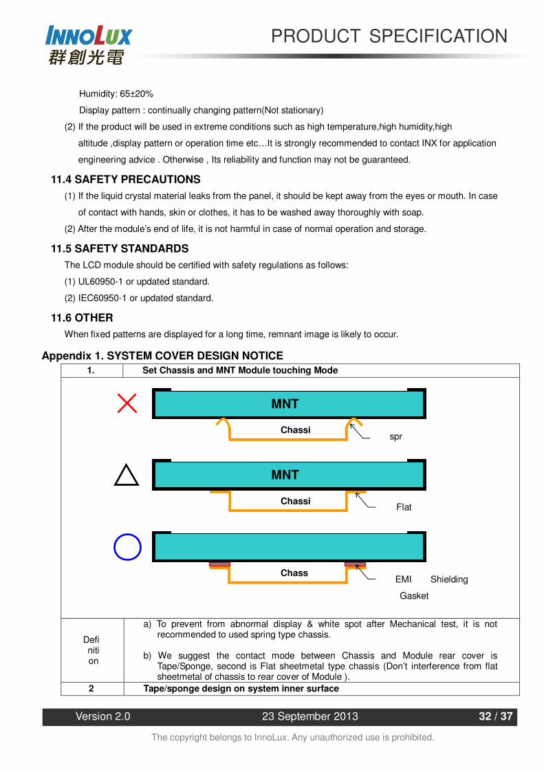
Appendix 1. SYSTEM COVER DESIGN NOTICE 1. Set Chassis and MNT Module touching Mode
Definition
a) To prevent from abnormal display & white spot after Mechanical test, it is not recommended to used spring type chassis.
b) We suggest the contact mode between Chassis and Module rear cover is
Tape/Sponge, second is Flat sheetmetal type chassis (Don’t interference from flat sheetmetal of chassis to rear cover of Module ).
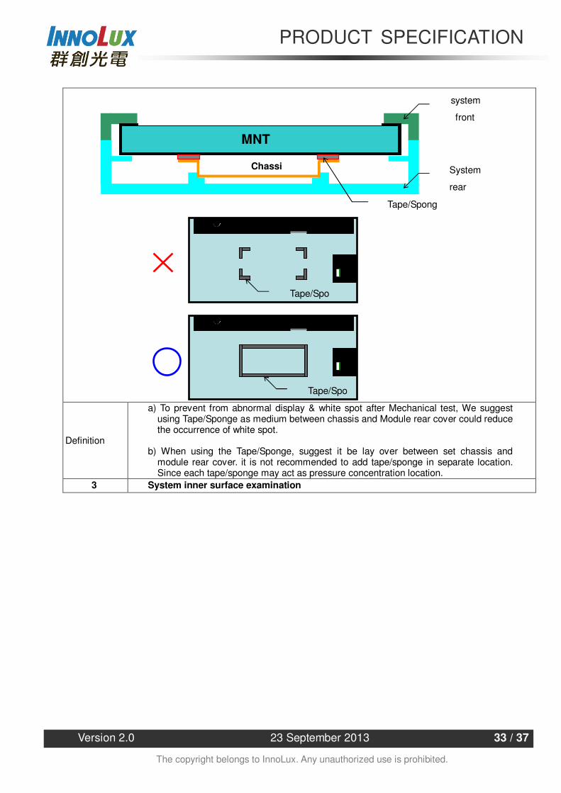
2 Tape/sponge design on system inner surface
MNT
ChassEMI Shielding
Gasket
MNT
Chassispr
MNT
ChassiFlat
PRODUCT SPECIFICATION
Version 2.0 23 September 2013 33 / 37
The copyright belongs to InnoLux. Any unauthorized use is prohibited.
Definition
a) To prevent from abnormal display & white spot after Mechanical test, We suggest using Tape/Sponge as medium between chassis and Module rear cover could reduce the occurrence of white spot.
b) When using the Tape/Sponge, suggest it be lay over between set chassis and
module rear cover. it is not recommended to add tape/sponge in separate location. Since each tape/sponge may act as pressure concentration location.
3 System inner surface examination
system
front
bezel
System
rear
MNT
Chassi
Tape/Spong
Tape/Spo
Tape/Spo
PRODUCT SPECIFICATION
Version 2.0 23 September 2013 34 / 37
The copyright belongs to InnoLux. Any unauthorized use is prohibited.
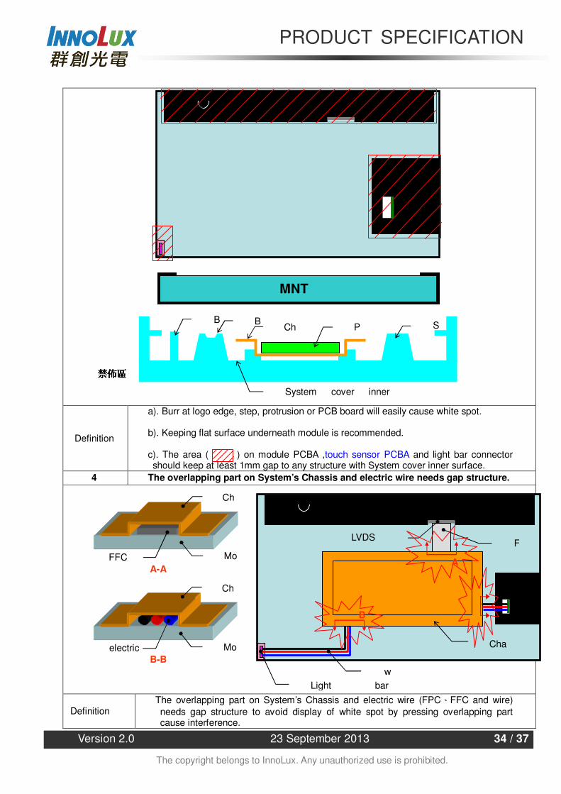
Definition
a). Burr at logo edge, step, protrusion or PCB board will easily cause white spot. b). Keeping flat surface underneath module is recommended. c). The area ( ) on module PCBA ,touch sensor PCBA and light bar connector should keep at least 1mm gap to any structure with System cover inner surface.
4 The overlapping part on System’s Chassis and electric wire needs gap structure.
Definition The overlapping part on System’s Chassis and electric wire (FPCFFC and wire) needs gap structure to avoid display of white spot by pressing overlapping part cause interference.
MNT
SBP
BCh
System cover inner
Mo
Ch
electric B-B
A-A
Ch
MoFFC
Cha
F
wLight bar
LVDS
B
A
PRODUCT SPECIFICATION
Version 2.0 23 September 2013 35 / 37
The copyright belongs to InnoLux. Any unauthorized use is prohibited.
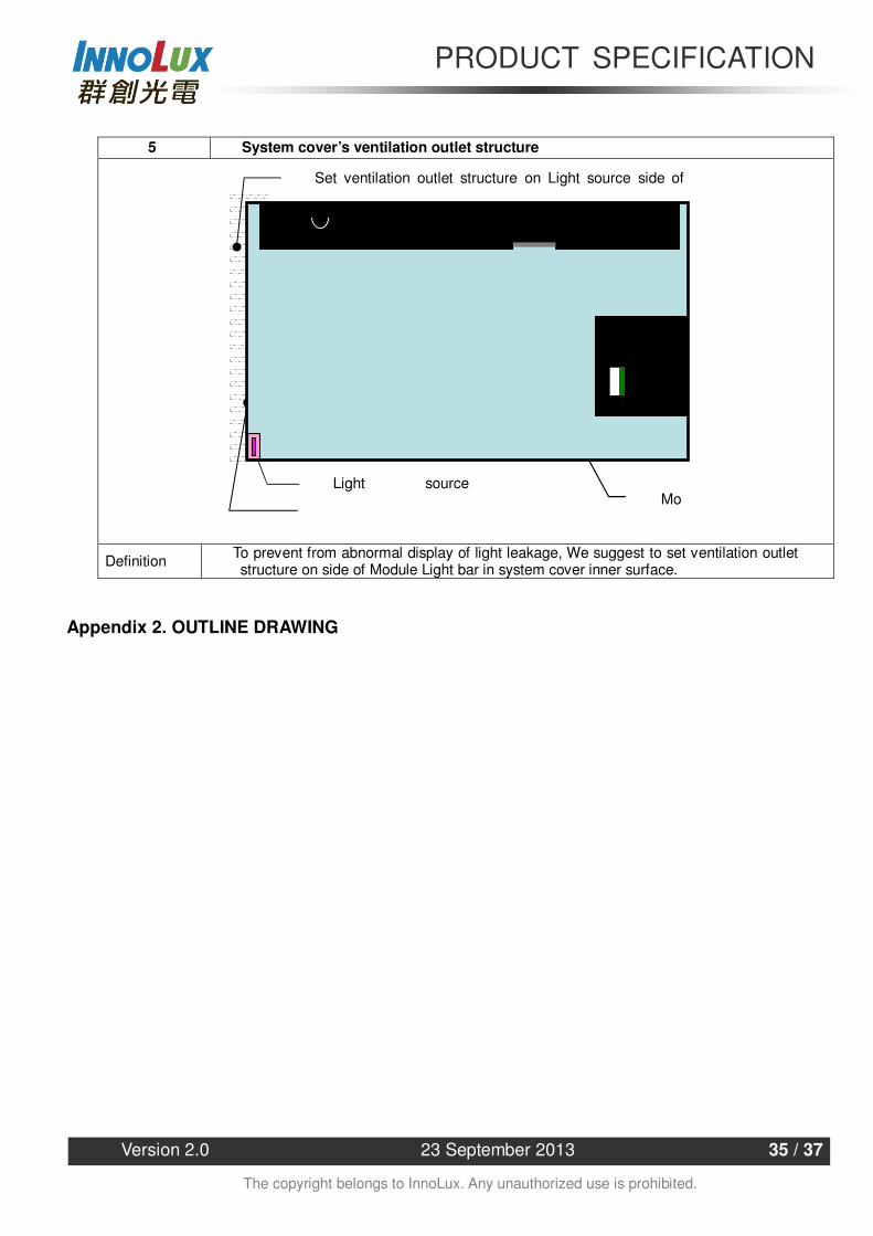
5 System cover’s ventilation outlet structure
Definition To prevent from abnormal display of light leakage, We suggest to set ventilation outlet structure on side of Module Light bar in system cover inner surface.
Appendix 2. OUTLINE DRAWING
MoLight source
Set ventilation outlet structure on Light source side of