Embed Size (px)
Citation preview

OLED SPECIFICATION
WEA012864LWPP3N00000
■APPROVAL FOR SPECIFICATIONS ONLY
□APPROVAL FOR SPECIFICATIONS AND
SAMPLE ( )
Model No:

SPECIFICATION Version: D
SALES BY
APPROVED BY
CHECKED BY
PREPARED BY
RELEASE DATE:
■APPROVAL FOR SPECIFICATIONS ONLY
□APPROVAL FOR SPECIFICATIONS AND SAMPLE
CUSTOMER :
MODULE NO. : WEA012864LWPP3N00000
APPROVED BY:
( FOR CUSTOMER USE ONLY )

WEA012864LWPP3N00000 第 1 頁,共 24頁
MODEL NO:
RECORDS OF REVISION DOC. FIRST ISSUE
VERSION DATE REVISED PAGE NO.
SUMMARY
0 2020/02/11 First release
A 2020/08/28 Modify Inspection specification
B 2020/11/18 Modify Storage Precautions
C 2020/11/19 Modify Contrast Ratio
D 2021/02/25 Modify Precautions in use of OLED Modules
WEA012864LWPP3N00000 第 2 頁,共 24頁
Contents
1.Module Classification Information
2.General Specification
3.Contour Drawing & Block Diagram
4.Interface Pin Function
5.Absolute Maximum Ratings
6.Electrical Characteristics
7.Optical Characteristics
8.OLED Lifetime
9.Reliability
10.Inspection specification
11.Precautions in use of OLED Modules
WEA012864LWPP3N00000 第 3 頁,共 24頁
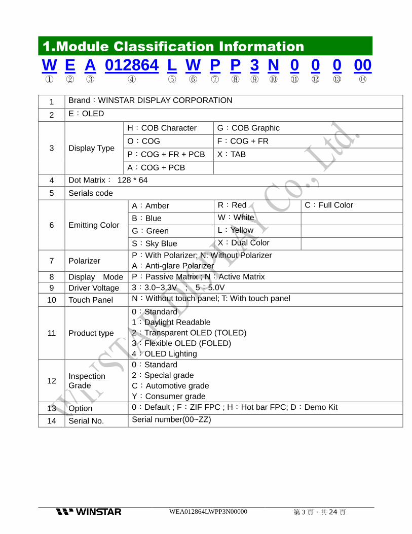
1.Module Classification Information
W E A 012864 L W P P 3 N 0 0 0 00 ① ② ③ ④ ⑤ ⑥ ⑦ ⑧ ⑨ ⑩ ⑪ ⑫ ⑬ ○14
1 Brand:WINSTAR DISPLAY CORPORATION
2 E:OLED
3 Display Type
H:COB Character G:COB Graphic
O:COG F:COG + FR
P:COG + FR + PCB X:TAB
A:COG + PCB
4 Dot Matrix: 128 * 64
5 Serials code
6 Emitting Color
A:Amber R:Red C:Full Color
B:Blue W:White
G:Green L:Yellow
S:Sky Blue X:Dual Color
7 Polarizer P:With Polarizer; N: Without Polarizer
A:Anti-glare Polarizer
8 Display Mode P:Passive Matrix ; N:Active Matrix
9 Driver Voltage 3:3.0~3.3V ; 5:5.0V
10 Touch Panel N:Without touch panel; T: With touch panel
11 Product type
0:Standard
1:Daylight Readable
2:Transparent OLED (TOLED)
3:Flexible OLED (FOLED)
4:OLED Lighting
12 Inspection Grade
0:Standard
2:Special grade
C:Automotive grade
Y:Consumer grade
13 Option 0:Default ; F:ZIF FPC ; H:Hot bar FPC; D:Demo Kit
14 Serial No. Serial number(00~ZZ)
WEA012864LWPP3N00000 第 4 頁,共 24頁
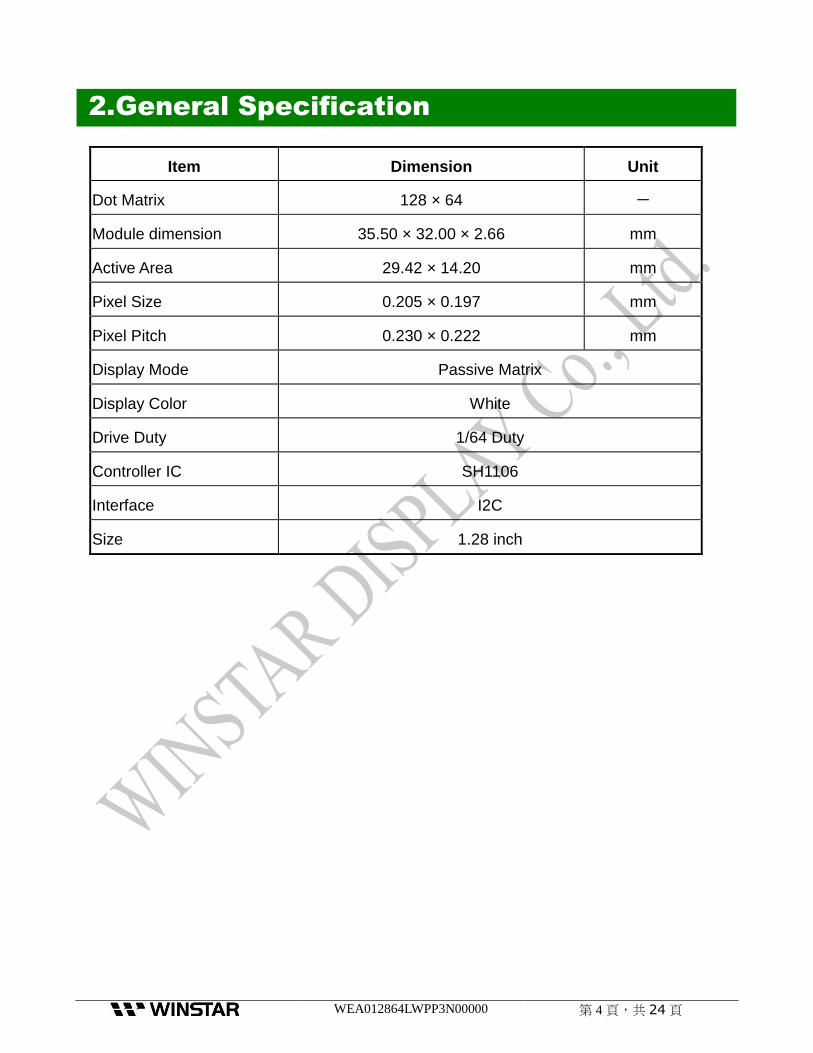
2.General Specification
Item Dimension Unit
Dot Matrix 128 × 64 -
Module dimension 35.50 × 32.00 × 2.66 mm
Active Area 29.42 × 14.20 mm
Pixel Size 0.205 × 0.197 mm
Pixel Pitch 0.230 × 0.222 mm
Display Mode Passive Matrix
Display Color White
Drive Duty 1/64 Duty
Controller IC SH1106
Interface I2C
Size 1.28 inch

WEA012864LWPP3N00000 第 5 頁,共 24頁
3. Contour Drawing & Block Diagram
SCL
4
3
2
1
GND
SDA
Scale 20/1
0.205
0.23
0.1
97
0.2
22
VCC
Active Area 1.28"128*64 Dots
23
±0
.2
15
.62
(V
A)
14
.2 (
AA
)34.5±0.2
33.5 (Pol.)
29.42 (AA)
31.32 (VA) 1.59
0.5
2.54
18
.2 (
Po
l.)
1.6
4
2.3
5
0.5
Pull tape
1.66
WEA012864LWPP3N00000
EA012864L-ASM2-01
華凌光電股份有限公司WINSTAR DISPLAY CO.
OLED MODULE
DWG NO.
TITLE
MODEL1/1
The non-specified tolerance of dimension is ±0.3 mm .
0REV:
1/1SCALE: mmUNIT:
PAGE:
DRAWN
CHECKED
APPROVED
Purry
41 14
30 1
27
.7
1.7
0.5±0.5
35.5±0.5
32
±0
.5
4.5
±0
.5
2.1
5
5.05
3.3
25.4 2.2
R1.1
4-R2.
5
13.94
1(10)(15.5)
1
Power supply
IC
Operating Temperature
Storage Temperature
Interface Jack
William
-40 C ~80 C
-40 C ~85 C
Color
SH1106G
2
3
4
5
6
WHITE
3V
I2C
Component area
Height=2.5 max.
7.5±0.5
Scale 1/1
SDA SCL GND VCC
1.5
6
2
P2.54*(4-1)=7.62
2.540.64
2019.7.17
2.66±0.3
WEA012864LWPP3N00000 第 6 頁,共 24頁
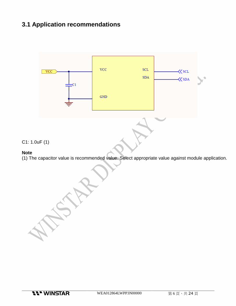
3.1 Application recommendations
C1: 1.0uF (1) Note (1) The capacitor value is recommended value. Select appropriate value against module application.

WEA012864LWPP3N00000 第 7 頁,共 24頁
4. Interface Pin Function
No. Symbol Function
1 VCC Power supply input
2 GND Ground
3 SCL The serial clock input
4 SDA The serial data input

WEA012864LWPP3N00000 第 8 頁,共 24頁
5.Absolute Maximum Ratings
Parameter Symbol Min Max Unit Notes
Supply Voltage for Logic VCC 1.65 5.5 V 1,2
Operating Temperature TOP -40 +80 °C —
Storage Temperature TSTG -40 +85 °C —
Note 1: All the above voltages are on the basis of “VSS = 0V”. Note 2: When this module is used beyond the above absolute maximum ratings, permanent
breakage of the module may occur. Also, for normal operations, it is desirable to use this module under the conditions according to Section 6.“Optics & Electrical Characteristics”. If this module is used beyond these conditions, malfunctioning of the module can occur and the reliability of the module may deteriorate.

WEA012864LWPP3N00000 第 9 頁,共 24頁
6.Electrical Characteristics
6.1 DC Electrical Characteristics
Item Symbol Condition Min Typ Max Unit
Supply Voltage for Logic VCC - 2.9 3.3 5.2 V
Input High Volt. VIH - 0.8×VCC - VCC V
Input Low Volt. VIL - 0 - 0.2×VCC V
Output High Volt. VOH - 0.8×VCC - VCC V
Output Low Volt. VOL - 0 - 0.2×VCC V
50% Check Board operating Current
ICC VCC =3.3V - 25 37.5 mA

WEA012864LWPP3N00000 第 10 頁,共 24頁
6.2 Initial code
void INIT_SH1106(){
WriteCommand(0xAE); // display OFF
WriteCommand(0xB0); //set page address WriteCommand(0x10); //set higher column address WriteCommand(0x00); //set lower column address WriteCommand(0xA4); //set entire display off WriteCommand(0xD5); //set display clock divide ratio/osc frequency WriteCommand(0x50); WriteCommand(0xA8); //Select Multiplex Ratio WriteCommand(0x3F); //64Duty WriteCommand(0xD3); //display offset,set to 0x00 WriteCommand(0x00); WriteCommand(0x40); //set start line,set to 0x40 WriteCommand(0xAD); //set DC-DC WriteCommand(0x8A); //8B: ON ; 8A: OFF WriteCommand(0xA1); //set segment re-map,SEG131~S0 WriteCommand(0xC8); //set common output scan direction; WriteCommand(0xDA); //common pad configuration WriteCommand(0x12); WriteCommand(0x81); //set contrast WriteCommand(0xFF); WriteCommand(0xD9); //set dis-charge/pre-charge period WriteCommand(0x11); WriteCommand(0xDB); //set VCOM deselect level WriteCommand(0x35); WriteCommand(0xA6); //set normal display WriteCommand(0xAF); //display ON } Note: Initial code is for reference only. Please make the best adjustment with the OLED module.

WEA012864LWPP3N00000 第 11 頁,共 24頁
7.Optical Characteristics
Item Symbol Condition Min Typ Max Unit
View Angle
(V)θ - 160 - - deg
(H)φ - 160 - - deg
Contrast Ratio CR Dark 10,000:1 - - -
Response Time
T rise - - 10 - μs
T fall - - 10 - μs
Display with 50% check Board Brightness 60 80 - cd/m2
CIEx(White) (CIE1931) 0.26 0.28 0.30 -
CIEy(White) (CIE1931) 0.30 0.32 0.34 -

WEA012864LWPP3N00000 第 12 頁,共 24頁
8.OLED Lifetime
ITEM Conditions Min Typ Remark
Operating Life Time
Ta=25°C / Initial 50% check board brightness Typical Value
20,000 Hrs - Note
Notes: 1. Life time is defined the amount of time when the luminance has decayed to <50% of the
initial value. 2. This analysis method uses life data obtained under accelerated conditions to extrapolate
an estimated probability density function (pdf) for the product under normal use conditions.
3. Screen saving mode will extend OLED lifetime.

WEA012864LWPP3N00000 第 13 頁,共 24頁
9.Reliability
Content of Reliability Test
Environmental Test
Test Item Content of Test Test Condition Applicable Standard
High Temperature storage
Endurance test applying the high storage temperature for a long time.
85°C 240hrs
——
Low Temperature storage
Endurance test applying the low storage temperature for a long time.
-40°C 240hrs
——
High Temperature Operation
Endurance test applying the electric stress (Voltage & Current) and the thermal stress to the element for a long time.
80°C 240hrs
——
Low Temperature Operation
Endurance test applying the electric stress under low temperature for a long time.
-40°C 240hrs
——
High Temperature/ Humidity Storage
Endurance test applying the high temperature and high humidity storage for a long time.
60°C,90%RH 240hrs
——
High Temperature/ Humidity Operation
Endurance test applying the high temperature and high humidity Operation for a long time.
60°C,90%RH 120hrs
——
Temperature Cycle
Endurance test applying the low and high temperature cycle. -40°C 25°C 80°C 30min 5min 30min 1 cycle
-40°C /80°C 30 cycles
——
Mechanical Test
Vibration test Endurance test applying the vibration during transportation and using.
Frequency:10~55Hz amplitude:1.5mm Time:0.5hrs/axis Test axis:X,Y,Z
——
Others
Static electricity test
Endurance test applying the electric stress to the finished product housing.
Air Discharge model ±4kv,10 times
——
*** Supply voltage for OLED system =Operating voltage at 25°C

WEA012864LWPP3N00000 第 14 頁,共 24頁
Test and measurement conditions 1. All measurements shall not be started until the specimens attain to temperature stability.
After the completion of the described reliability test, the samples were left at room temperature for 2 hrs prior to conducting the failure test at 23±5°C; 55±15% RH.
2. All-pixels on/off exchange is used as operation test pattern. 3. The degradation of Polarizer are ignored for High Temperature storage, High Temperature/
Humidity Storage, Temperature Cycle Evaluation criteria 1. The function test is OK. 2. No observable defects. 3. Luminance: > 50% of initial value. 4. Current consumption: within ± 50% of initial value.
APPENDIX: RESIDUE IMAGE Because the pixels are lighted in different time, the luminance of active pixels may reduce or differ from inactive pixels. Therefore, the residue image will occur. To avoid the residue image, every pixel needs to be lighted up uniformly.

WEA012864LWPP3N00000 第 15 頁,共 24頁
10.Inspection specification
Inspection Standard: MIL-STD-105E table normal inspection single sample level II.
Definition 1 Major defect : The defect that greatly affect the usability of product. 2 Minor defect : The other defects, such as cosmetic defects, etc.
Definition of inspection zone:
Zone A: Active Area Zone B: Viewing Area except Zone A Zone C: Outside Viewing Area Note: As a general rule, visual defects in Zone C are permissible, when it is no trouble of
quality and assembly to customer`s product.
Inspection Methods 1 The general inspection : Under fluorescent light illumination: 750~1500 Lux, about 30cm viewing distance, within 45º viewing angle, under 25±5°C.
2 The luminance and color coordinate inspection : By SR-3 or BM-7 or the equal equipments, in the dark room, under 25±5°C.
NO Item Criterion AQL
01 Electrical Testing
1.1 Missing vertical, horizontal segment, segment contrast defect. 1.2 Missing character , dot or icon. 1.3 Display malfunction. 1.4 No function or no display. 1.5 Current consumption exceeds product specifications. 1.6 OLED viewing angle defect. 1.7 Mixed product types. 1.8 Contrast defect.
0.65
02
Black or white spots on OLED (display only)
2.1 White and black spots on display ≦ 0.25mm, no more than three white or black spots present. 2.2 Densely spaced: No more than two spots or lines within 3mm.
2.5
C B A

WEA012864LWPP3N00000 第 16 頁,共 24頁
NO Item Criterion AQL
03
OLED black spots, white spots, contamination (non-display)
3.1 Round type : As following drawing Φ=( x + y ) / 2
SIZE Acceptable QTY
Zone
Φ≦0.10 ignore A+ B
0.10<Φ≦0.20 2 A+ B
0.20<Φ≦0.25 1 A+ B
0.25<Φ 0 A+ B
2.5
3.2 Line type : (As following drawing)
Length Width Acceptable Q TY
Zone
--- W≦0.02 ignore A+B
L≦3.0 0.02<W≦0.03 2
A+B
L≦2.5 0.03<W≦0.05 A+B
--- 0.05<W As round type
2.5
04 Polarizer bubbles /Dent
4.1 If bubbles are visible, judge using black spot specifications, not easy to find, must check in specify direction. 4.2 The polarizer dent follows this specification.
Size Φ Acceptable Q TY Zone
Φ≦0.20 ignore A+B
0.20<Φ≦0.50 3 A+B
0.50<Φ≦1.00 2 A+B
1.00<Φ 0 A+B
Total Q TY 3
2.5
05 Scratches Follow NO.3 OLED black spots, white spots, contamination.

WEA012864LWPP3N00000 第 17 頁,共 24頁
NO Item Criterion AQL
06 Chipped glass
Symbols Define: x: Chip length y: Chip width z: Chip thickness k: Seal width t: Glass thickness a: OLED side length L: Electrode pad length: 6.1 General glass chip : 6.1.1 Chip on panel surface and crack between panels:
z: Chip thickness y: Chip width x: Chip length
Z≦1/2t Not over viewing area x≦1/8a
1/2t<z≦2t Not exceed 1/3k x≦1/8a
☉If there are 2 or more chips, x is total length of each chip.
6.1.2 Corner crack:
z: Chip thickness y: Chip width x: Chip length
Z≦1/2t Not over viewing area x≦1/8a
1/2t<z≦2t Not exceed 1/3k x≦1/8a
☉If there are 2 or more chips, x is the total length of each chip.
2.5
06 Glass crack
Symbols : x: Chip length y: Chip width z: Chip thickness k: Seal width t: Glass thickness a: OLED side length L: Electrode pad length 6.2 Protrusion over terminal : 6.2.1 Chip on electrode pad :
y: Chip width x: Chip length z: Chip thickness
y≦0.5mm x≦1/8a 0 < z ≦ t
2.5
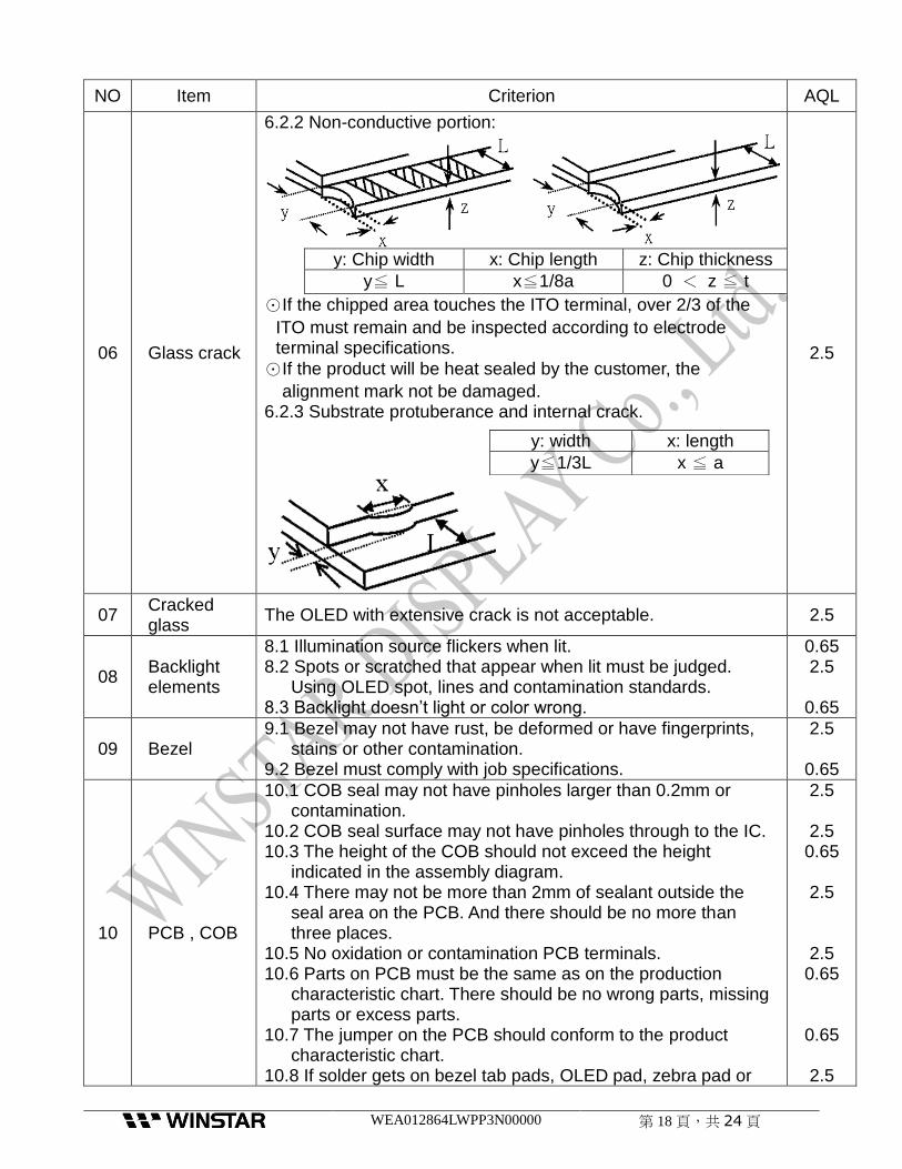
WEA012864LWPP3N00000 第 18 頁,共 24頁
NO Item Criterion AQL
06 Glass crack
6.2.2 Non-conductive portion:
y: Chip width x: Chip length z: Chip thickness
y≦ L x≦1/8a 0 < z ≦ t
☉If the chipped area touches the ITO terminal, over 2/3 of the
ITO must remain and be inspected according to electrode terminal specifications.
☉If the product will be heat sealed by the customer, the
alignment mark not be damaged. 6.2.3 Substrate protuberance and internal crack.
y: width x: length
y≦1/3L x ≦ a
2.5
07 Cracked glass
The OLED with extensive crack is not acceptable. 2.5
08 Backlight elements
8.1 Illumination source flickers when lit. 8.2 Spots or scratched that appear when lit must be judged.
Using OLED spot, lines and contamination standards. 8.3 Backlight doesn’t light or color wrong.
0.65 2.5
0.65
09 Bezel 9.1 Bezel may not have rust, be deformed or have fingerprints,
stains or other contamination. 9.2 Bezel must comply with job specifications.
2.5
0.65
10 PCB , COB
10.1 COB seal may not have pinholes larger than 0.2mm or contamination.
10.2 COB seal surface may not have pinholes through to the IC. 10.3 The height of the COB should not exceed the height
indicated in the assembly diagram. 10.4 There may not be more than 2mm of sealant outside the
seal area on the PCB. And there should be no more than three places.
10.5 No oxidation or contamination PCB terminals. 10.6 Parts on PCB must be the same as on the production
characteristic chart. There should be no wrong parts, missing parts or excess parts.
10.7 The jumper on the PCB should conform to the product characteristic chart.
10.8 If solder gets on bezel tab pads, OLED pad, zebra pad or
2.5
2.5 0.65
2.5
2.5 0.65
0.65
2.5

WEA012864LWPP3N00000 第 19 頁,共 24頁
screw hold pad, make sure it is smoothed down.

WEA012864LWPP3N00000 第 20 頁,共 24頁
NO Item Criterion AQL
11 Soldering
11.1 No un-melted solder paste may be present on the PCB. 11.2 No cold solder joints, missing solder connections, oxidation
or icicle. 11.3 No residue or solder balls on PCB. 11.4 No short circuits in components on PCB.
2.5 2.5
2.5
0.65
12 General appearance
12.1 No oxidation, contamination, curves or, bends on interface
Pin (OLB) of TCP. 12.2 No cracks on interface pin (OLB) of TCP. 12.3 No contamination, solder residue or solder balls on product. 12.4 The IC on the TCP may not be damaged, circuits. 12.5 The uppermost edge of the protective strip on the interface
pin must be present or look as if it cause the interface pin to sever.
12.6 The residual rosin or tin oil of soldering (component or chip component) is not burned into brown or black color.
12.7 Sealant on top of the ITO circuit has not hardened. 12.8 Pin type must match type in specification sheet. 12.9 OLED pin loose or missing pins. 12.10 Product packaging must the same as specified on
packaging specification sheet. 12.11 Product dimension and structure must conform to product
specification sheet.
2.5
0.65 2.5
2.5 2.5
2.5
2.5 0.65 0.65 0.65
0.65

WEA012864LWPP3N00000 第 21 頁,共 24頁
Check Item Classification Criteria
No Display Major
Missing Line Major
Pixel Short Major
Darker Short Major
Wrong Display Major
Un-uniform B/A x 100% < 70% A/C x 100% < 70%
Major

WEA012864LWPP3N00000 第 22 頁,共 24頁
11.Precautions in use of OLED Modules
Modules
(1) Avoid applying excessive shocks to module or making any alterations or modifications to it. (2) Don’t make extra holes on the printed circuit board, change the components or modify its
shape of OLED display module. (3) Don’t disassemble the OLED display module. (4) Do not apply input signals while the logic power is off. (5) Don’t operate it above the absolute maximum rating. (6) Don’t drop, bend or twist OLED display module. (7) Soldering: only to the I/O terminals. (8) Hot-Bar FPC soldering condition: 280~350C, less than 5 seconds. (9) Winstar has the right to change the passive components (Resistors, capacitors and other
passive components will have different appearance and color caused by the different supplier.) and change the PCB Rev. (In order to satisfy the supplying stability, management optimization and the best product performance...etc, under the premise of not affecting the electrical characteristics and external dimensions, Winstar have the right to modify the version.)
(10) Winstar has the right to upgrade or modify the product function. (11) For COG & COF structure OLED products, customers should reserve VCC (VPP) adjustment
function or software update function when designing OLED supporting circuit. (The progress of OLED light-emitting materials will increase the conversion efficiency and the brightness. The brightness can be adjusted if necessary).
11.1. Handling Precautions (1) Since the display panel is being made of glass, do not apply mechanical impacts such as
dropping from a high position. (2) If the display panel is broken by some accident and the internal organic substance leaks out,
be careful not to inhale nor lick the organic substance. (3) If pressure is applied to the display surface or its neighborhood of the OLED display module,
the cell structure may be damaged. So, be careful not to apply pressure to these sections. (4) The polarizer covering the surface of the OLED display module is soft and easily scratched. (5) When the surface of the polarizer of the OLED display module has soil, clean the surface. It
takes advantage by using following adhesion tape. * Scotch Mending Tape No. 810 or an equivalent Never try to breathe upon the soiled surface nor wipe the surface using cloth containing solvent such as ethyl alcohol, since the surface of the polarizer will become cloudy. Also, pay attention that the following liquid and solvent may spoil the polarizer: * Water * Ketone * Aromatic Solvents
(6) Protection film is being applied to the surface of the display panel and removes the protection film before assembling it. At this time, if the OLED display module has been stored for a long period of time, residue adhesive material of the protection film may remain on the surface of the display panel after removed of the film. In such case, remove the residue material by the method introduced in the above Section 5.
(7) Do not touch the following sections whenever possible while handling the OLED display modules. * Pins and electrodes

WEA012864LWPP3N00000 第 23 頁,共 24頁
* Pattern layouts such as the TCP & FPC (8) Hold OLED display module very carefully when placing OLED display module into the
System housing. Do not apply excessive stress or pressure to OLED display module. And, do not over bend the film with electrode pattern layouts. These stresses will influence the display performance. Also, secure sufficient rigidity for the outer cases.
(9) Do not apply stress to the LSI chips and the surrounding molded sections. (10) Pay sufficient attention to the working environments when handing OLED display modules
to prevent occurrence of element breakage accidents by static electricity. * Be sure to make human body grounding when handling OLED display modules. * Be sure to ground tools to use or assembly such as soldering irons. * To suppress generation of static electricity, avoid carrying out assembly work under dry environments. * Protective film is being applied to the surface of the display panel of the OLED display module. Be careful since static electricity may be generated when exfoliating the protective film.
11.2. Storage Precautions (1) When storing OLED display modules, put them in static electricity preventive bags to avoid
be directly exposed to sun or lights of fluorescent lamps. And, also, place in the temperature 25±5°C and Humidity below 65% RH.(We recommend you to store these modules in the packaged state when they were shipped from Winstar. At that time, be careful not to let water drops adhere to the packages or bags.)
(2) When the OLED display module is being dewed or when it is placed under high temperature or high humidity environments, the electrodes may be corroded if electric current is applied. Please store it in clean environment.
11.3. Designing Precautions (1) The absolute maximum ratings are the ratings which cannot be exceeded for OLED display
module, and if these values are exceeded, OLED display module may be damaged. (2) To prevent occurrence of malfunctioning by noise, pay attention to satisfy the VIL and VIH
specification and to make the signal line cable as short as possible. (3) We recommend you to install excess current preventive unit (fuses, etc.) to the power circuit
(VDD / VCC). (Recommend value: 0.5A) (4) Pay sufficient attention to avoid occurrence of mutual noise interference with the nearby
devices. (5) As for EMI, take necessary measures on the equipment side basically. (6) If the power supplied to the OLED display module is forcibly shut down by such errors as
taking out the main battery while the OLED display panel is in operation, we cannot guarantee the quality of this OLED display module. * Connection (contact) to any other potential than the above may lead to rupture of the IC.

WEA012864LWPP3N00000 第 24 頁,共 24頁
(7) If this OLED driver is exposed to light, malfunctioning may occur and semiconductor elements may change their characteristics.
(8) The internal status may be changed, if excessive external noise enters into the module. Therefore, it is necessary to take appropriate measures to suppress noise generation or to protect module from influences of noise on the system design.
(9) We recommend you to make periodical refreshment of the operation statuses (re-setting of the commands and re-transference of the display data) to cope with catastrophic noise.
(10) It's pretty common to use "Screen Saver" to extend the lifetime and Don't use the same image for long time in real application. When an OLED display module is operated for a long of time with fixed pattern, an afterimage or slight contrast deviation may occur.
(11) The limitation of FPC and Film bending.
(12) The module should be fixed balanced into the housing, or the module may be twisted.
(13) Please heat up a little the tape sticking on the components when removing it; otherwise the
components might be damaged.
11.4. Precautions when disposing of the OLED display modules (1) Request the qualified companies to handle industrial wastes when disposing of the OLED
display modules. Or, when burning them, be sure to observe the environmental and hygienic laws and regulations.
0.1
(0.1
Max
.)