Embed Size (px)
Citation preview
Modeling and characterization of
nanoelectromechanical systems
Martin Duemling
Thesis submitted to the Faculty of the
Virginia Polytechnic Institute and State University
in partial fulfillment of the requirements for the degree of
Masters of Science
in
Materials Science and Engineering
Dr. Stephane Evoy, Chair
Dr. James R. Heflin
Dr. William T. Reynolds, Jr.
August 15, 2002
Blacksburg, Virginia
Keywords: Nanotechnology, Nanomechanical resonator, NEMS
Copyright 2002, Martin Duemling
Modeling and characterization of
nanoelectromechanical systems
Martin Duemling
(Abstract)
Microelectromechanical structures (MEMS) are used commercially in sensor applications
and in recent years much research effort has been done to implement them in wireless
communication. Electron beam lithography and other advancements in fabrication
technology allowed to shrink the size of MEMS to nanomechanical systems (NEMS).
Since NEMS are just a couple of 100 nm in size, highly integrated sensor applications
are possible. Since NEMS consume only little energy, this will allow continuous
monitoring of all the important functions in hospitals, in manufacturing plants, on
aircrafts, or even within the human body.
This thesis discusses the modeling of NEM resonators. Loss mechanisms of
macroscale resonators, and how they apply to NEM resonators, will be reviewed.
Electron beam lithography and the fabrication process of Silicon NEM resonator will be
described. The emphasis of this work was to build a test setup for temperature dependant
measurements. Therefore different feasible techniques to detect nanoscale vibration will
be compared and the setup used in this work will be discussed. The successful detection
of nanoscale vibration and preliminary results of the temperature dependence of the
quality factor of a paddle resonator will be reported. A new approach to fabricate NEM
resonator using electrofluidic assembly will be introduced.

iii
To my wife
iv
Acknowledgements
I would like to thank my advisor Dr. Stephane Evoy for his encouragement, guidance and
support throughout the work, especially his continued support after he left Virginia Tech
to join the University of Pennsylvania. Dr. James R. Heflin I thank for the space in his
lab, his equipment and for handling all the money concerns after Dr. Evoy left. In
addition I am thankful to my other committee member Dr. William T. Reynolds.
I would like to thank all the people who supported this work with their knowledge
and time. Steve McCartney for teaching me electron microscopy, for his help in setting
up the electron beam lithography tool and for giving me access to the microscope around
the clock. Fred A. Mahone from the physics electronic shop for his quick response to my
inquiries and for all the answers to my questions regarding the measurement equipment.
Melvin Shaver, Scott Allen and John Miller from the physics machine shop for their help
and input in building the setup. Dan Huff from the packaging lab for giving me access to
the wirebonder. Dr. Hendricks and David Gray for the access to the clean room.
Christopher Maxey for running the FEM simulation of the paddle resonators for me. Ben
Hailer and Benjamin R. Martin, Thomas E. Mallouk, Irena Kratochvilova and Theresa S.
Mayer from Penn State University for fabricating and assembling the rhodium NEMS.
Anatoli Olkhovets and Harold Craighead from Cornell University for making silicon
NEMS available to us to test our characterization setup. William D. Barnhart for the
things he taught me regarding the silicon fabrication process. The particle physics group
of Virginia Tech for their vacuum equipment and especially Mark Makela for his help
with the equipment. Martin Drees for his help with the cryostat and other lab concerns.
Ingrid Burbey and Martin Phelan for revising my thesis.
This work was funded by the electrical engineering departments of Virginia Tech and
Upenn and by Oak Ridge National Laboratory and supported by the physics department
of Virginia Tech.
v
Contents
1 Introduction........................................................................................................... 1
1.1 Application of MEMS................................................................................. 1
1.2 Nanoelectromechanical structures .............................................................. 3
1.3 Overview of this thesis................................................................................ 4
2 Theory of vibration ............................................................................................... 6
2.1 Theory of elasticity of beams and cantilever .............................................. 6
2.1.1 Euler-Bernoulli law of elementary beam theory............................. 7
2.1.2 Damping of an Euler-Bernoulli beam........................................... 13
2.1.3 Timoshenko beam......................................................................... 14
2.1.4 Empirical approaches for a cantilever........................................... 15
2.2 Classical Harmonic Oscillation................................................................. 17
2.3 Application to nanomechanical paddles ................................................... 21
2.3.1 Translational motion ..................................................................... 22
2.3.2 Torsional motion........................................................................... 27
3 Loss mechanisms................................................................................................. 33
3.1 Energy dissipation and quality factor ....................................................... 34
3.2 Air friction ................................................................................................ 35
3.2.1 Viscous region .............................................................................. 35
3.2.2 Molecular region........................................................................... 36
3.2.3 Squeeze force ................................................................................ 37
3.3 Clamping................................................................................................... 38
3.4 Phonon-Phonon Scattering........................................................................ 39
3.5 Phonon-Electron Scattering ...................................................................... 39
3.6 High temperature background................................................................... 39
vi
3.7 Surface related effects............................................................................... 40
3.7.1 Thin film on surface...................................................................... 40
3.7.2 Metal layer .................................................................................... 40
3.7.3 Oxide layer.................................................................................... 41
3.7.4 Water layer.................................................................................... 41
3.8 Summary ................................................................................................... 42
4 Stress relaxation .................................................................................................. 43
4.1 Mathematical description of relaxation .................................................... 44
4.2 Thermoelastic relaxation........................................................................... 49
4.3 Defect Relaxation...................................................................................... 51
4.4 Grain boundary relaxation ........................................................................ 52
4.5 Summary ................................................................................................... 54
5 Device fabrication and setup.............................................................................. 55
5.1 Electron beam lithography........................................................................ 55
5.1.1 Electron-Solid-Interaction............................................................. 56
5.1.2 Strategy to avoid the proximity effect .......................................... 57
5.2 Virginia Tech EBL system........................................................................ 57
5.3 Surface machining of NEMS .................................................................... 58
5.4 Testing of nanomechanical structures....................................................... 59
5.4.1 Capacitive detection...................................................................... 59
5.4.2 Magnetic detection........................................................................ 60
5.4.3 Electron beam detection................................................................ 61
5.4.4 Optical detection methods............................................................. 61
5.4.5 Interferometry method .................................................................. 62
vii
5.5 Experimental setup.................................................................................... 64
5.5.1 Electrostatical actuation ................................................................ 64
5.5.2 Room temperature setup ............................................................... 65
5.5.3 Low temperature setup.................................................................. 66
5.5.4 Modeling of optical response........................................................ 68
5.5.5 Sensitivity of the Detector ............................................................ 71
5.5.6 Electrical calibration ..................................................................... 72
5.5.7 Temperature calibration ................................................................ 73
6 Testing of nanomechanical paddle resonators ................................................. 74
6.1 Preliminary assessment of resonant modes............................................... 75
6.1.1 Room temperature setup ............................................................... 75
6.1.2 In the low temperature setup......................................................... 75
6.2 DC dependence measurements ................................................................. 77
6.3 Low temperature measurements ............................................................... 79
6.4 Conclusion ................................................................................................ 80
7 Rhodium NEMS.................................................................................................. 81
7.1 Fabrication and assembly.......................................................................... 81
7.2 Nanomechanical testing of rhodium NEMS ............................................. 84
7.3 Discussion ................................................................................................. 84
7.4 Outlook ..................................................................................................... 85
8 Improvements of the Setup ................................................................................ 86
8.1 Optical....................................................................................................... 86
8.2 Electrical ................................................................................................... 87
8.3 Room temperature setup ........................................................................... 87
8.4 Low temperature setup.............................................................................. 88
8.5 New detection method .............................................................................. 89
9 Conclusion and further work............................................................................. 90
9.1 Further work.............................................................................................. 91
viii
List of figures
Figure 2.1 Flexural behavior of a straight beam (a) and its stress distribution (b) ............. 7
Figure 2.2 Strain in a cantilever .......................................................................................... 9
Figure 2.3 Geometry of a paddle (the thickness of the paddle is a and the gap between
substrate and the resonator is h) (a) and the modes of its motion (b) ............ 22
Figure 2.4 Olkhovets model for the translation mode of the paddle ................................ 23
Figure 2.5 Dowell model of a paddle................................................................................ 24
Figure 2.6 Results of the FEM simulation of the translational mode, resonant frequency
(a) and stress distribution (b) ......................................................................... 25
Figure 2.7 Results of the FEM simulation of the butterfly mode, resonant frequency (a)
and stress distribution (b)............................................................................... 26
Figure 2.8 Torsional model of paddle............................................................................... 28
Figure 2.9 Results of the FEM simulation with an asymmetry of 50 nm, resonant
frequency (a) and stress distribution (top view) (b) and with an asymmetry of
10 nm (c)........................................................................................................ 32
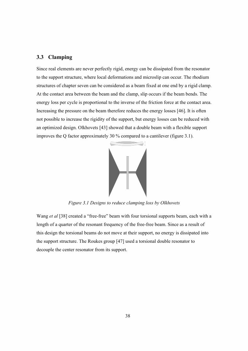
Figure 3.1 Designs to reduce clamping loss by Olkhovets............................................... 38
Figure 4.1 Influence of an applied stress to the energy levels of a system....................... 44
Figure 4.2 Hook’s element (a), Newton’s element (b), St. Venenat element (c) and the
rheological representations of the Zener model (d) ....................................... 45
Figure 4.3 Stress relaxation and creep of a Zener solid .................................................... 46
Figure 4.4 ωτ (a) and temperature (b) dependence of the Debye relaxation curves for
internal friction (α) and dynamic modulus (β) .............................................. 47
Figure 4.5 Schematic illustration of a disordered atom group model............................... 53
Figure 5.1 First structure written with EBL at Virginia Tech a) using NPGS b) using the
SEM alone, PMMA as negative resist. .......................................................... 58
Figure 5.2 Principle of a deflection system used in an AFM and change of reflection of a
beam............................................................................................................... 62
ix
Figure 5.3 Principle of a Farby-Perot interferometer........................................................ 63
Figure 5.4 Electrostatical actuation................................................................................... 64
Figure 5.5 Experimental setup for room temperature measurements ............................... 66
Figure 5.7 Change of intensity with a change of the optical path length.......................... 70
Figure 5.9 Temperature calibration setup (a) and results (b)............................................ 73
Figure 6.1 Geometry of a paddle (not visible in the picture: the thickness of the paddle a
and the gap between substrate and the resonator h) ...................................... 74
Figure 6.2 Resonance peak of room temperature measurements ..................................... 75
Figure 6.3 Change of Amplitude for different applied voltages (a) ................................. 76
Figure 6.4 Detector output at resonance versus driving term (a) and he resonance peak of
two different modes (b) ................................................................................. 77
Figure 6.5 Frequency dependence on the applied DC potential ....................................... 78
Figure 6.6 Temperature dependence of Q-factor and frequency ...................................... 80
Figure 7.1 Rhodium NEMS .............................................................................................. 81
Figure 7.2 Top- and cross-sectional views of the electrodes structure ............................. 82
Figure 7.3 Destroyed electrodes ....................................................................................... 83
x
List of tables
Table 2.1 Solution of the equation of motion for a cantilever beam ................................ 13
Table 2.2 Comparison of an Euler-Bernoulli beam with the analytical solution for a free-
free rectangular beam .................................................................................... 16
Table 2.3 Comparison of different models for a paddle oscillator ................................... 27
Table 2.4 Comparison of the torsional resonant frequency of two different models with an
FEM simulation ............................................................................................. 30
Table 5.1 Intensity of the reflected light from the resonator ............................................ 69
Table 5.2 Absorption coefficient of the optical parts measured with a Filmetrics ........... 69
1
1 Introduction
“There’s plenty of room at the Bottom” was the title of a talk given by Richard Feynman
in December 1959 [1]. Since then many things he had envisioned have become true. Sub-
micron circuits are commercially employed in computers. It is even possible to freely
place single atoms on a substrate [2]. However, while there is still plenty of room at the
bottom, there is even more in-between. In solid state physics, for example, as long as a
system can be approximated as infinite, its behavior can be explained and predicted fairly
well. At the other end systems consisting of a few electrons or an atom can be described
by particle or molecular physics. In between these two regions lies the mesoscopic
region, where the classical theories break down but where systems are already too large
to apply straightforward quantum mechanics. In the mesoscopic region many questions
remain unanswered. The best understood mesoscopic systems are electric systems
(quantum dots, quantization of electrical conductance)[3]. Recently the first step to a
theory of thermal conductance in the mesoscopic regime was reported [4]. But the
mechanical behavior of mesoscopic system leaves many questions open. These questions
will be addressed in this work.
1.1 Application of MEMS
The term MEMS (microelectromechanical structure) describes devices where a
mechanical function is coupled with an electrical signal. These MEMS are used in a wide
range of applications: from sensors using the change of resistance or capacitance [5],
motors [6], applications for fluid transport [7], switches [8], phase shifters [9] or even
2
optical switches in fiber communication [10]. A subgroup of MEMS are MEM
resonators. These resonators are used in sensors [5] and in wireless communication [9].
Sensing functions can also be accomplished by monitoring changes in resonant frequency
due to either forces on the resonator or through mass absorption. An example of a force
sensor is an atomic force microscope (AFM) [11]. If the force between the atoms of the
sample and the tip changes, so does the frequency of the resonator. An AFM has a
resolution in the nano Newton range. In pressure sensors the force is due to the
interaction of the surface with the surrounding gas [5]. The force on the resonator is
pressure dependent and therefore pressure changes are accompanied by a change of the
resonant frequency. Gas sensors are coated with an active layer that attracts certain gas
molecules [12]. This additional mass changes also the resonant frequency. Since
different molecules are absorbed by different coatings, gas sensors can be made for very
specific gases. Biological sensors work in a similar way. There the resonator is coated
with an immobilized antibody. These sensors achieve a sensitivity of a few cells [13].
While gas sensors are commercially available, biological sensors are still in development.
Angular acceleration can be measured with microgyrometers [5]. In a
microgryrometer, a mass supported by a spring in the x and y direction, rotates around
the z-axis. The amplitude of the x and y oscillation is proportional to the rotation around
the z-axis.
Resonators can be used in wireless communication as filters [9], oscillators [9] and
mixers [9]. A resonator will only resonate around its resonant frequency. This property is
utilized in filters. In a filter the input signal is used to excite the resonator and the output
signal is coupled to the amplitude response of the resonator. This way signals with
frequencies away from the resonant frequency are filtered out. A resonator in connection
with a feedback amplifier can be used as an oscillator. The output signal of an oscillator
has the resonant frequency of the resonator. This signal can be used as a carrier frequency
in wireless communication. A mixer has two input signals with two different frequencies
and the output signal will be the sum of the signals but with another frequency [14]. So
far MEM resonators are not used in wireless communication application. One of the
main reasons for this is that the integration with the integrated circuitry (IC) is difficult.
To integrate sensors the electronics are often built on one chip and the actual sensor on
3
another, the two chips are than wirebonded together [16]. This method is not feasible for
wireless communication, because the advantage of size reduction compared to quartz
resonators would be lost. Also the frequency regime of MEM resonators limits their
possible functions in wireless communication.
1.2 Nanoelectromechanical structures
Reducing the size of a resonator increases its resonant frequency. Since frequencies in the
GHZ range are possible, NEM resonators are envisioned for RF or microwave
communication. A consequence of the smaller mass of the resonator is that smaller
changes in the mass can be detected, which enables an NEM resonator to detect masses
approaching the level of single atoms [17]. Charges can also be detected with NEM
resonators with an ultimate sensitivity of an electron [18].
Another possible application of NEM resonators is magnetic resonant force
microscopy (MRFM) [17]. In MRFM the interaction of the intrinsic magnetic moment
(spin) of a nuclei with an applied magnetic field is utilized. With today’s technique
(nuclear magnetic resonant spectrometry (NMR)) a response of 1014 – 1016 nuclei
generates a measurable signal (which leads to a resolution of 10 µm). Sidles (1991) has
shown theoretically that a sensitivity down to the spin of a single proton can be achieved
with a mechanical detection method. If a nanomagnet is used to provide a magnetic field,
it can vary so strongly in space that the nuclear resonant condition is satisfied only in the
volume of an atom, a 3D mapping of individual biomolecules would be therfore possible.
The tiny back action of the interaction of the spin with the external magnetic field results
in a vibration of the cantilever. It is already possible to measure the magnitude of forces
that result from a single resonant nucleus (10-18 N) [19].
Another interesting aspect of NEM resonators is that they allow research on quantum
mechanical resonators. In the millikelvin range the thermal energy (kT) of a GHz range
NEM resonator is in the order of the energy quantum (hv). There the thermal fluctuations
will be smaller than the intrinsic quantum noise. So the square amplitude of the vibration
should be quantized, only having values that are multiples of hfQ/2 keff. Transducers that
4
measure the position squared are only a factor 100 away from the sensitivity that is
needed to measure displacement in the quantum domain (10-27 m2) [20][17].
Another advantage of NEMS is their low energy consumption, even a million
nanomechanical elements would dissipate only a millionth of a watt. This could lead to
miniature sensors with low power consumption. Important functions in hospitals, in
manufacturing plants, on aircrafts, or even within the human body could be continuously
monitored with these sensors [21].
The size reduction also brings some major challenges. If the frequency is changed by
a few additional atoms on the surface, it will be difficult to mass-produce resonators with
the same properties. The communication with the macro world is already challenging in
MEMS application and will increase further for NEMS devices: For example, a signal of
the magnitude of a few electrons can get easily obscured by thermal vibration.
At present our understanding of nano mechanical systems is very limited. For
example the quality factor of microelectromechanical (MEM) resonators is around 1011 at
cryogenic temperatures, reducing the size of the resonator to a nano level decreases the
quality factor to less than 107 [17]. Since the percentage of surface and near surface
atoms increases with decreasing size, the decrease of the quality factor is probably
surface related, but its precise origin is not known yet [17].
This work had three goals. The first goal was to setup an electron beam lithography
tool and to develop a nanofabrication process. The second was to review existing
vibration models and to develop an adequate model of the vibration of NEM resonators.
The last and most important goal was to develop a test setup for temperature-dependent
experimental testing of NEM resonators.
1.3 Overview of this thesis
The mechanical properties of NEM resonators will be discussed in chapter two. First the
resonant frequency of the resonator is derived using elasticity and simple beam theory.
Then it will be shown that these more complex mechanical systems can be approximated
as simple harmonic oscillators. In chapter three and four the main mechanisms that
contribute to energy dissipation in an NEM resonator will be discussed. Chapter three
concentrates on the more general and fundamental loss mechanisms, while in chapter
5
four relaxation phenomena are discussed. Chapter five describes the device fabrication
and the experimental setup. In chapter six the results of the experiments are discussed. It
will be shown that we were able to measure the resonant frequency and the quality factor
of NEM resonators as a function of temperature. Chapter seven is dedicated to an
alternative fabrication method based on the self-assembly of rhodium rods. Finally this
work will conclude with a discussion of possible improvements of the setup (chapter
eight) and further work that must be done to obtain a better understanding of NEM
resonators (chapter nine).
6
2 Theory of vibration
For designing and modeling a device based on an NEM resonator, a theoretical
understanding of its vibration is necessary. A theoretical understanding of vibration is
also necessary for a correct interpretation of experimental data. In part 2.1.1, the resonant
frequency of a cantilever beam will be derived using simple beam theory and elasticity.
The remaining part of 2.1 will review approaches to overcome the limitation of the
simple beam theory and how damping can be introduced into simple beam theory. In part
2.2, it will be shown that a resonator can be approximated as a simple harmonic
oscillator. The model of a simple harmonic oscillator will than be used in part 2.3 to
model the resonant behavior of paddle resonators.
2.1 Theory of elasticity of beams and cantilever
Simple beam-theory is restricted to a prismatic (equal cross section), homogeneous,
straight and untwisted structure. The thickness (d) and width (w) have to be small
compared to the length (l), which reduces the problem to an one-dimensional problem
along the length of the beam. Furthermore it is assumed that the normal stresses (σ) in the
x and y direction can be neglected [22]. The following derivation only holds if the
maximum deflection (in x) is smaller than the radius of gyration (K). If the maximum
deflection approaches K, additional non-linear terms must be considered [23]. The
coordinate system used for the following derivation is shown in figure 2.1.
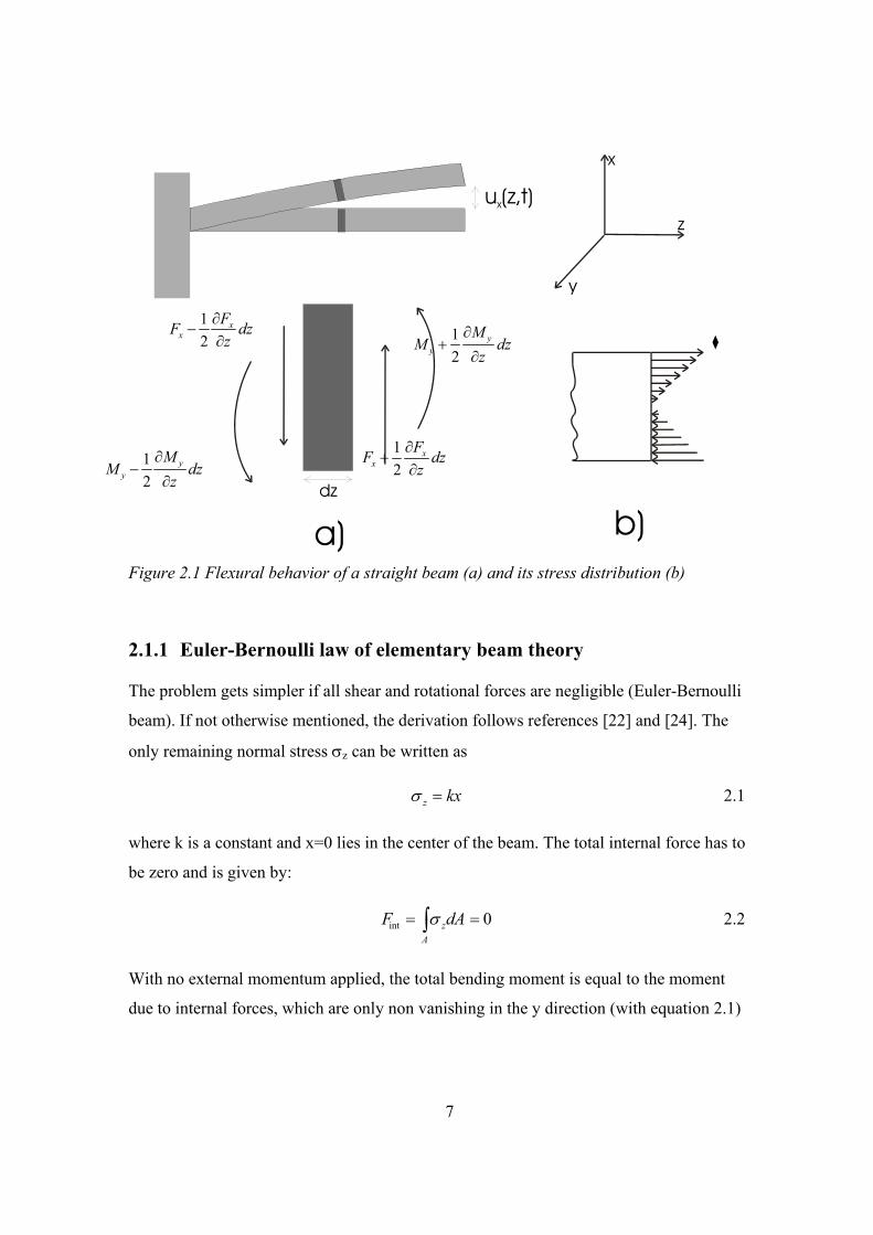
7
z
y
x
u (z,t)x
dz
a) b)
Figure 2.1 Flexural behavior of a straight beam (a) and its stress distribution (b)
2.1.1 Euler-Bernoulli law of elementary beam theory
The problem gets simpler if all shear and rotational forces are negligible (Euler-Bernoulli
beam). If not otherwise mentioned, the derivation follows references [22] and [24]. The
only remaining normal stress σz can be written as
z kxσ = 2.1
where k is a constant and x=0 lies in the center of the beam. The total internal force has to
be zero and is given by:
Fint = σ zA∫ dA = 0 2.2
With no external momentum applied, the total bending moment is equal to the moment
due to internal forces, which are only non vanishing in the y direction (with equation 2.1)
12
yy
MM dz
z∂
−∂
12
xx
FF dzz
∂+
∂
12
xx
FF dzz
∂−
∂ 12
yy
MM dz
z∂
+∂
8
M = My = xσ zdAA∫ = k x2dA
A∫ 2.3
The moment of inertia is defined as:
Iy = x2
A∫ dA 2.4
substituting equation 2.4 into 2.3 defines k as:
k =My
Iy
2.5
The stress of the cross section is therefore given by:
σz =MyxIy
2.6
Using Hook’s law the strain (ε) can be calculated
εz =σ z
E=
My xEIy
2.7
where E is Young’s modulus.
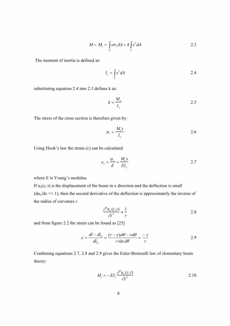
If ux(z, t) is the displacement of the beam in x direction and the deflection is small
(dux/dx << 1), then the second derivative of the deflection is approximately the inverse of
the radius of curvature r
∂ 2ux (z, t)∂z 2 ≈
1r
2.8
and from figure 2.2 the strain can be found as [25]
rx
drrddxr
dldldl −
=−−
=−
=θ
θθεsin)(
0
0 2.9
Combining equations 2.7, 2.8 and 2.9 gives the Euler-Bernoulli law of elementary beam
theory:
My = −EIy∂2ux (z, t)∂z 2 2.10
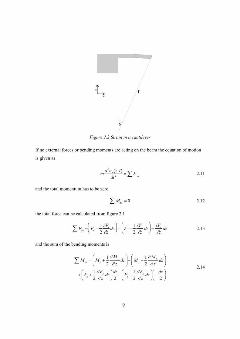
9
Figure 2.2 Strain in a cantilever
If no external forces or bending moments are acting on the beam the equation of motion
is given as
2
2 int
( , )xd u z tm Fdt
= ∑ 2.11
and the total momentum has to be zero
Mint = 0∑ 2.12
the total force can be calculated from figure 2.1
Fint =∑ Fx +12∂Fx
∂zdz
− Fx −
12∂Fx
∂zdz
=
∂Fx
∂zdz 2.13
and the sum of the bending moments is
int
1 12 2
1 12 2 2 2
y yy y
x xx x
M MM M dz M dz
z z
F Fdz dzF dz F dzz z
∂ ∂∂ ∂
∂ ∂∂ ∂
= + − −
+ + − − −
∑ 2.14
10
Equations 2.14 and 2.12 combined give the relationship between the bending moment
and the force
Fx = −∂My
∂z 2.15
With equation 2.15, 2.13 and the mass m=ρAdz (where ρ is the density and A the cross
section), the equation of motion (equation 2.11) becomes
2
2
2
2 ),(zM
tdtzud
A yx
∂∂
ρ −= 2.16
Now My can be replaced in equation 2.16 with 2.10, which leads to the final equation of
motion
ρAd2ux(z, t)
d2t+ EIy
∂ 4ux(z, t)∂z4 = 0 2.17
This harmonic linear 4th order differential equation can be solved using separation of
variables [22] [24]. In this work we are not concerned with the complete solution, but
only the natural resonant frequency of the beam. The natural resonant frequency can be
easily obtained by using a Fourier transformation. Applying a Fourier transformation to
equation 2.17 with Φ (ux(z,t))=Ux(z,ω) leads to
ρA iω( )2U x(z,ω) + EIy∂ 4Ux (z,ω)
∂z 4 = 0 2.18
The calculation becomes simpler if the equation is rewritten as
−α 4ω x2Ux (z,ω ) +
∂ 4Ux (z,ω )∂z 4 = 0 2.19
with
α =ρAEIy
4 2.20
The solution of this differential equation is
11
Ux(z,ω) = A1eαz ω + A2e
−αz ω + A3eiαz ω + A4e
− iαz ω 2.21
where A1, A2 ,A3 ,A4 are complex constants which can be determined by the boundary
condition. Using the Euler equations and the comparable equations for sinh and cosh
(sinh x =e x − e− x
2 and cosh x =
ex + e− x
2) equation 2.21 can be transformed to an
equation with real constants B1, B2, B3, B4
Ux(z,ω) = B1 sin(αz ω ) + B2 cos(αz ω ) + B3 sinh(αz ω ) + B4 cosh(αz ω ) 2.22
By applying the boundary conditions of the problem to equation 2.22, the resonant
frequency can be found. In the following a cantilever will be considered. Since at the
clamped side of the cantilever (z=0) no displacement takes place and the beam is straight,
the boundary conditions are given by
(0, ) 0 (0, ) 0xx
dUUdz
ω ω= = 2.23
At the free end of the beam (z=L), there is no bending moment and no shear forces that
act on the beam
d2Ux( l,ω )
dz2 = 0 dUx
3(l,ω )dz3 = 0 2.24
From the first two boundary conditions, it follows that B2=B4 and B1=-B3. The last two
boundary conditions reduce equation 2.22 to
2 + 2cos(αl ω )cosh(αl ω )
sin(αl ω ) − sinh(αl ω )= 0 2.25
A non-trivial solution can be found if
cos(αl ω )cosh(αl ω ) = −1 2.26
12
This equation has no analytical solution but can be solved numerical by using the
following substitution
β = αl ω 2.27
The values for βi can be found in table 2.1. From equation 2.20 and 2.19 the natural
resonant frequency and its harmonics can be calculated:
ω i =βi
l2
2 EIy
ρA 2.28
The moment of inertia of a beam with circular cross section is given by
4
64ydI π
= 2.29
where d is the diameter of the beam and the inertia with a rectangular cross section is
3
12ywtI = 2.30
For a beam clamped on both sides the boundary conditions are
(0, ) 0 (0, ) 0 ( , ) 0 ( , ) 0x xx x
dU dUU U L Ldz dz
ω ω ω ω= = = = 2.31
and for a beam free on both sides the boundary conditions are
2 3 2 3
2 3 2 3
(0, ) (0, ) ( , ) ( , )0 0 0 0x x x xd U dU d U l dU ldz dz dz dz
ω ω ω ω= = = = 2.32
The solution method is similar to the one for the cantilever. The final solution is the same
for the clamped-clamped and the free-free beam and only differs from the cantilever in
the factor βi,, whose values are also listed in table 2.1.
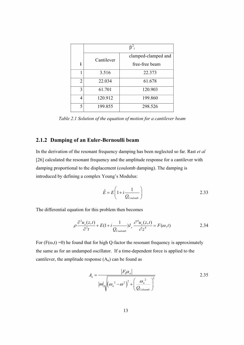
13
β2i
i Cantilever
clamped-clamped and
free-free beam
1 3.516 22.373
2 22.034 61.678
3 61.701 120.903
4 120.912 199.860
5 199.855 298.526
Table 2.1 Solution of the equation of motion for a cantilever beam
2.1.2 Damping of an Euler-Bernoulli beam
In the derivation of the resonant frequency damping has been neglected so far. Rast et al
[26] calculated the resonant frequency and the amplitude response for a cantilever with
damping proportional to the displacement (coulomb damping). The damping is
introduced by defining a complex Young’s Modulus:
1ˆ 1Coulomb
E E iQ
= +
2.33
The differential equation for this problem then becomes
2 4
2 4
( , ) ( , )1(1 ) ( , )x xy
Coulomb
u z t u z tE i I F tt Q z
∂ρ ω∂
∂+ + =
∂ 2.34
For (F(ω,t) =0) he found that for high Q-factor the resonant frequency is approximately
the same as for an undamped oscillator. If a time-dependent force is applied to the
cantilever, the amplitude response (An) can be found as
( )
0
2222 2
nn
nn
Coloumb
FA
mQ
α
ωω ω
=
− +
2.35
14
where ωn is the resonant frequency of the cantilever and αn is a constant depending on the
boundary condition (i.e. the form of the applied force). As seen later, this equation has
the same form as the solution of the simple harmonic oscillator. Therefore the cantilever
used in this thesis can be approximated with a simple harmonic oscillator.
2.1.3 Timoshenko beam
In the Euler-Bernoulli beam, the shear deformation of the beam was not taken into
account. Timoshenko developed a model to overcome that limitation. All other
limitations of the Euler-Bernoulli model still apply to the Timoshenko model. Only the
main steps are given here, and a more detailed derivation can be found in reference [22].
The shear deformation of the cross section acts in the opposite direction to the
deflection of the beam. The cross section is therefore not perpendicular to the (deformed)
beam as in the Euler-Bernoulli beam. The rotation can be written as:
xy x
uz
φ γ∂= −
∂ 2.36
where the shear strain is given by
γ x =
χFx
GA 2.37
and χ is the shear factor. This shear factor is dependent on the shape of the beam’s cross
section. G is the rigidity modulus, which is linked to Young’s modulus through the
Poisson ratio (µ) [27]:
G =E
2(1+ µ) 2.38
The bending moment then becomes
My = EIy∂∂z
∂ux
∂z−
TFx
GA
2.39
15
Another consequence of taking the rotational inertia of the cross section into account is
that the total moment of the beam is no longer equal to zero (as in equation 2.12) but
2
2y
yM I dzt
ρ∂ Φ
=∂∑ 2.40
With the sum of the force and the moment (equation 2.13 and 2.14) the two governing
equations become
2
2
2
2
( , )x x
y yy x
u z t Fmt z
MI F
t z
∂∂∂
ρ∂
∂=
∂∂ Φ
= +∂
2.41
With equation 2.36 and 2.37 equation 2.41 can be combined and solved for Fx
24 4 2 4 4
2 2 4 2 4 2 2 0y yx x x x xy y
I EIu u u u uI A EIz t G t t z G z t
ρ χ ρχ∂ ∂ ∂ρ ρ∂ ∂ ∂ ∂
∂ ∂− − − + =
∂ ∂ ∂ 2.42
This differential equation was first solved by Goen in 1931 [28]. Pickett [29] gives a
good summary of Goen's work and includes some application notes. Due to the length of
the solution for an actual thin beam, it is not included and only an advancement of this
solution is given in the next paragraph.
2.1.4 Empirical approaches for a cantilever
The Timoshenko beam is still an approximation and the solution found by Goen does not
fulfill all boundary conditions [29]. Since it is very difficult to find a model that
implements all material and geometric characteristics an empirical model is necessary.
This empirical relationship was determined by the American Society for Testing and
Materials (ASTM) [30] based on Goen's and Pickett's work. For a free-free beam with
rectangular cross section the resonant frequency can be found as
2
11.028( , )f
t Efl T t l ρ
= 2.43

16
Resonant frequency [MHz]
Euler-Bernoulli ASTM Relative error
Correction
factor T
l =1µm 1649.7 1469.6 0.12 1.260
l =4µm 103.1 102.2 0.008 1.017 t=200 nm
l =8µm 25.8 25.7 0.002 1.004
l =1µm 2886.8 2183.6 0.322 1.748
l =4µm 180.4 175.9 0.026 1.052 t=350 nm
l =8µm 45.1 44.8 0.006 1.013
Table 2.2 Comparison of an Euler-Bernoulli beam with the analytical solution for a free-
free rectangular beam
The equation differs from the resonant equation derived for an Euler-Bernoulli Beam
only by a correction factor T(t,l).
2 42
42
22
( , ) 1.000 6.585(1.000 0.075 0.811 ) 0.868
8.340(1.000 0.202 2.173 )
1.000 6.338(1 0.141 1.537 )
t tT t ll l
tl
tl
µ µ
µ µ
µ µ
= + + + −
+ + −
+ + +
2.44
It can be seen that for t << l the correction factor T becomes equal to 1. The correction
factor for an Euler-Bernoulli beam with a circular cross-section is given as
2 42
42
22
( , ) 1.000 4.939(1.000 0.075 0.811 ) 0.4883
4.691(1.000 0.202 2.173 )
1.000 4.754(1.000 0.141 1.537 )
d dT d ll l
dl
dl
µ µ
µ µ
µ µ
= + + + −
+ + −
+ + +
2.45
17
The experiments done by the ASTM to obtain the correction factor were done on a large
scale beam at low frequencies. Therefore it should be kept in mind that the correction
factors might have some errors if applied to high frequency NEMS and MEMS. The
ASTM standard assumes a homogeneous material. Due to the high surface to volume
ratio it is questionable whether an NEMS device could be assumed to be homogeneous.
Table 3.2 shows the error that is introduced by the Euler-Bernoulli approximation, which
is only significant for short beams.
2.2 Classical Harmonic Oscillation
As it can be seen from the complexity of the derivation of the resonant frequency it will
be difficult to model the behavior of these devices using continuous mechanics. It would
be desirable to describe the resonator using a system with one-degree of freedom. The
simplest one-degree of freedom system is a massless spring with a spring constant k and
a mass m attached to the spring. This oscillator will be discussed in detail here and we
will show that by adjusting the spring constant and the mass it can describe the vibration
of more complex structures like a cantilever or even paddle resonators. Neglecting
damping, the equation of motion of a harmonic oscillator is given as
2
2 ( ) ( ) 0dm x t kx tdt
+ = 2.46
The solution of this equation is
1 2( ) sin( ) cos( )k km mx t A t A t= + 2.47
Which leads to a resonant frequency of
ω0 =km
2.48
18
Comparing this equation with equation 2.43 shows that a beam resonator can be
approximated with a simple harmonic oscillator if an effective spring constant keff and an
effective mass meff is defined [31].
Almeff ρ= 2.49
4
3( , )yi
eff
EIk
T t l lβ
= 2.50
where βi depends on the mode and can be found in table 2.1. The damping can be
included in equation 2.46 by defining a complex spring constant for damping
proportional to the displacement (i.e. coloumb damping) [25]
1ˆ 1Coulomb
k k iQ
= +
2.51
By adding a frictional force that is proportional to the velocity (viscous damping) [32].
0( ) ( )frictionviscous
mF x t x tQωγ= =& & 2.52
The equation of motion with a periodical driving force is then
20 00
1( ) ( ) (1 ) ( ) i t
viscous Coulomb
Fx t x t i x t eQ Q m
ωω ω+ + + =&& & 2.53
The solution of this equation must have the following form
1 2( ) i t i tx t A e A eω ω−= + 2.54
To find the factors A1 and A2 equation 2.54 can be inserted into equation 2.53
f
f f
2 2 0 0 f1 0 f
2 2 0 0 f 02 0 f
- +i
- +i
i t
coloumb viscous
i t i t
coloumb viscous
A eQ Q
FA e eQ Q m
ω
ω ω
ω ω ωω ω
ω ω ωω ω −
− +
+ =
2.55
19
It follows that A2=0 and the solution for x(t) is therefore
( )
( ) ( ) f
122 2 3 4 2 20
0 f 0 f 0 f 0
2 2 20 f 0 f 0
( ) coloumb viscousviscous coloumb
viscous coloumb
i tviscous coloumb coloumb viscous
F Q Qx t Q Qm Q Q
Q Q i Q Q e ω
ω ω ω ω ω ω ω
ω ω ω ω ω
−
= − + + −
− + −
2.56
which can be rewritten as
( )1
2 22 22 2 ( )0 0 f 0f 0( ) i t
viscous coloumb
Fx t em Q Q
ω ψω ω ω ω ω
−
+ = − + −
2.57
where ψ is the phase difference
( ) ( )
21 0 f 0
2 2 2 20 f 0 f
tanviscous coloumbQ Q
ω ω ωψω ω ω ω
− = − − −
2.58
The actual amplitude of the vibration is then given by
0f 22
2 2 2 0 0 f0 f
1( )
( )coloumb viscous
FAm
Q Q
ωω ω ωω ω
=
− + +
2.59
For Qviscous=0 equation 2.59 is similar to the amplitude response calculated by Rast et al
(equation 2.35) [26]. Since it only differs by a proportionality factor that depends on the
form of the applied force and the boundary condition, beam resonators can be
approximated with a simple harmonic oscillator. Equation 2.59 shows that the frequency
where the amplitude is maximum is not at the resonant frequency ω0 but is actually
quality factor dependent. Since finding the resonant frequency is straightforward but
tedious, only the case where Qcloumb =0 will be considered here, which is
max 0 2
112
viscousQ
ω ω
= −
2.60
20
In the limit of a high quality factor (Q) the amplitude will only be significant for the
region where ωf≈ω0, therefore ωfω0≈ω02 and ωf+ω0≈2ω0. With this substitution equation
2.59 becomes
0f 2 2
0 f
0
1( )1 14
coloumb viscous
FAk
Q Q
ωω ω
ω
= −
+ +
2.61
In the limit of large Q we than find that
1
Qtot
=1
Qcoloumb
+1
Qviscous
2.62
and equation 2.61 becomes
0max f 2 2
0 f
0
1( )14tot
FAk
Q
ωω ω
ω
= −
+
2.63
Equation 2.63 has the form of a Lorentzian. The experimental data can be fitted to that
equation to obtain the Q factor and the resonant frequency. But from equation 2.63 a
quicker way to calculate Qtot can be derived. The maximum amplitude at resonance is
given by
0max tot
FA Qk
= 2.64
The amplitude is reduced to half its original value if
2 2
0
0
1 12 14
tot
half
tot
Q
Qω ω
ω
= −
+
2.65
or
0
0
3 14
half
totQω ω
ω−
= 2.66
21
The half bandwidth ∆ω is the peak width at half the amplitude and therefore
02( )halfω ω ω∆ = − 2.67
and the quality factor is given as
0 03 1.73tothalfbandwith halfbandwith
fQf
ωω
= = 2.68
This expression will be used later to calculate the Q factor from the data obtained in the
experiments.
2.3 Application to nanomechanical paddles
Paddle resonators are a better choice for sensor applications where high frequencies are
not necessary. The surface of a paddle is larger than the surface of a cantilever or a
double clamped beam, therefore their active sensing area is larger. The larger surface is
also interesting from a research point of view, as it allows the investigation of
interestinmg surface-related phenomena. In addition, the deflection also will be much
larger compared with the one of cantilevers or beams, which makes it easier to detect
their vibration. Hence paddle resonators have been chosen for these experimental studies.
It can be seen in figure 2.4b, that paddles resonate in two different modes, a torsional and
a translational mode. In the following, the two modes are discussed separately.
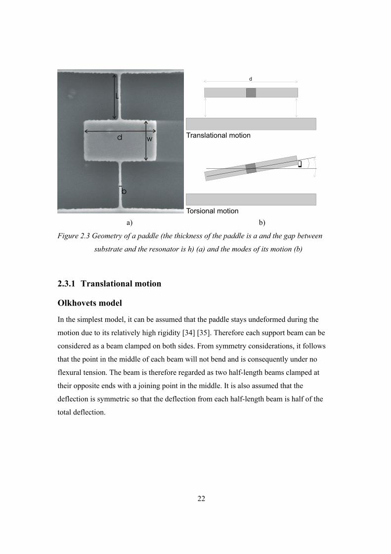
22
d w
L
b
Translational motion
d
Torsional motion a) b)
Figure 2.3 Geometry of a paddle (the thickness of the paddle is a and the gap between
substrate and the resonator is h) (a) and the modes of its motion (b)
2.3.1 Translational motion
Olkhovets model
In the simplest model, it can be assumed that the paddle stays undeformed during the
motion due to its relatively high rigidity [34] [35]. Therefore each support beam can be
considered as a beam clamped on both sides. From symmetry considerations, it follows
that the point in the middle of each beam will not bend and is consequently under no
flexural tension. The beam is therefore regarded as two half-length beams clamped at
their opposite ends with a joining point in the middle. It is also assumed that the
deflection is symmetric so that the deflection from each half-length beam is half of the
total deflection.
23
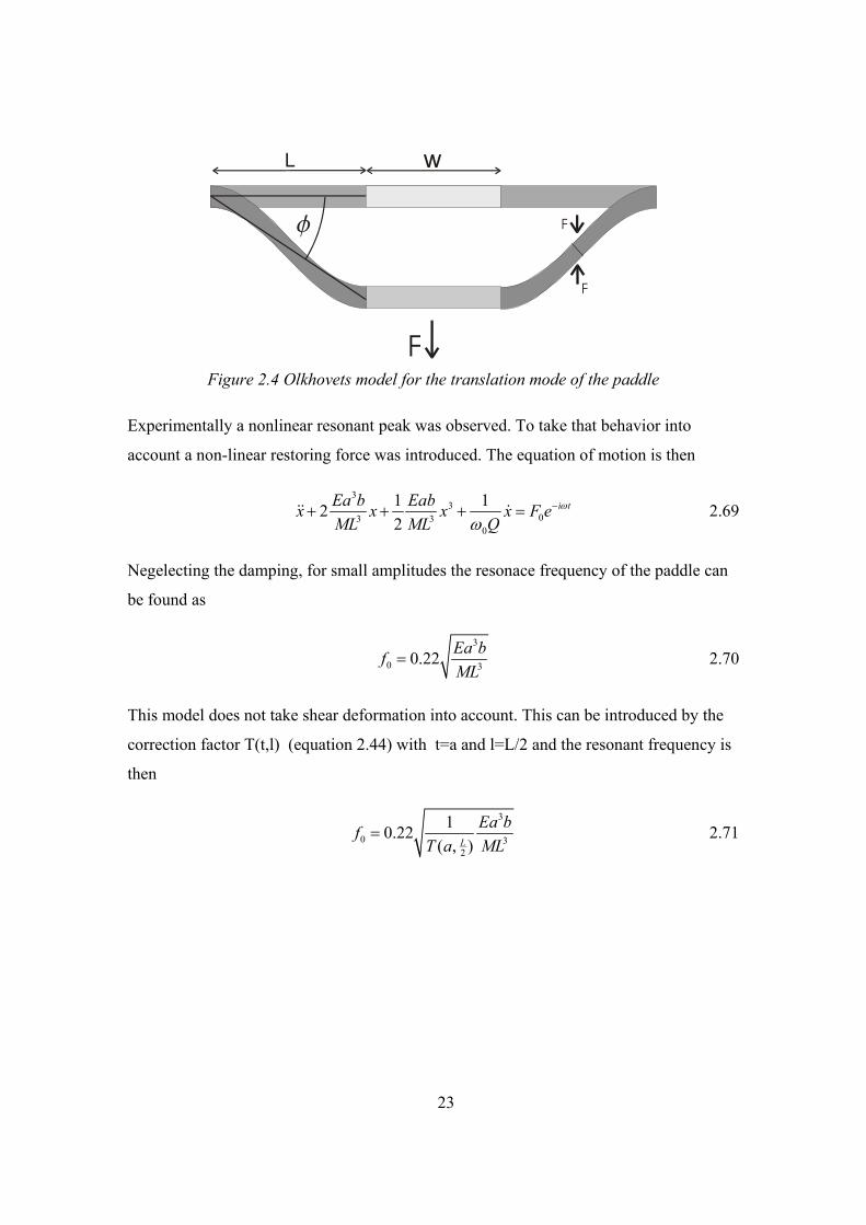
Figure 2.4 Olkhovets model for the translation mode of the paddle
Experimentally a nonlinear resonant peak was observed. To take that behavior into
account a non-linear restoring force was introduced. The equation of motion is then
3
303 3
0
1 122
i tEa b Eabx x x x F eML ML Q
ω
ω−+ + + =&& & 2.69
Negelecting the damping, for small amplitudes the resonace frequency of the paddle can
be found as
3
0 30.22 Ea bfML
= 2.70
This model does not take shear deformation into account. This can be introduced by the
correction factor T(t,l) (equation 2.44) with t=a and l=L/2 and the resonant frequency is
then
3
0 32
10.22( , )L
Ea bfT a ML
= 2.71
24
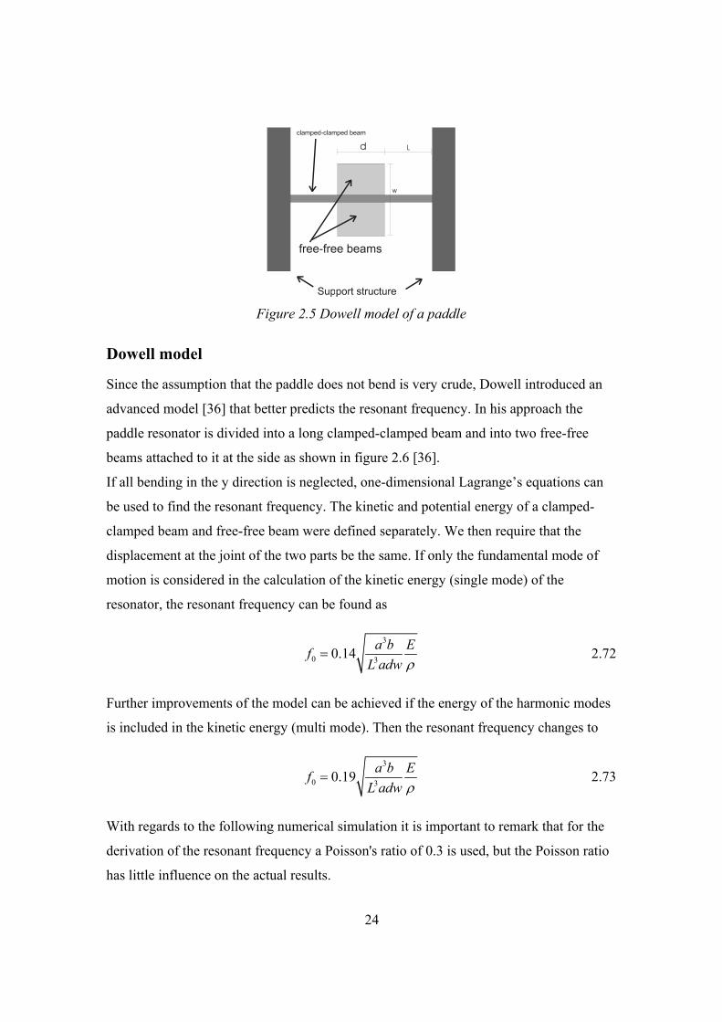
Figure 2.5 Dowell model of a paddle
Dowell model
Since the assumption that the paddle does not bend is very crude, Dowell introduced an
advanced model [36] that better predicts the resonant frequency. In his approach the
paddle resonator is divided into a long clamped-clamped beam and into two free-free
beams attached to it at the side as shown in figure 2.6 [36].
If all bending in the y direction is neglected, one-dimensional Lagrange’s equations can
be used to find the resonant frequency. The kinetic and potential energy of a clamped-
clamped beam and free-free beam were defined separately. We then require that the
displacement at the joint of the two parts be the same. If only the fundamental mode of
motion is considered in the calculation of the kinetic energy (single mode) of the
resonator, the resonant frequency can be found as
3
0 30.14 a b EfL adw ρ
= 2.72
Further improvements of the model can be achieved if the energy of the harmonic modes
is included in the kinetic energy (multi mode). Then the resonant frequency changes to
3
0 30.19 a b EfL adw ρ
= 2.73
With regards to the following numerical simulation it is important to remark that for the
derivation of the resonant frequency a Poisson's ratio of 0.3 is used, but the Poisson ratio
has little influence on the actual results.
25
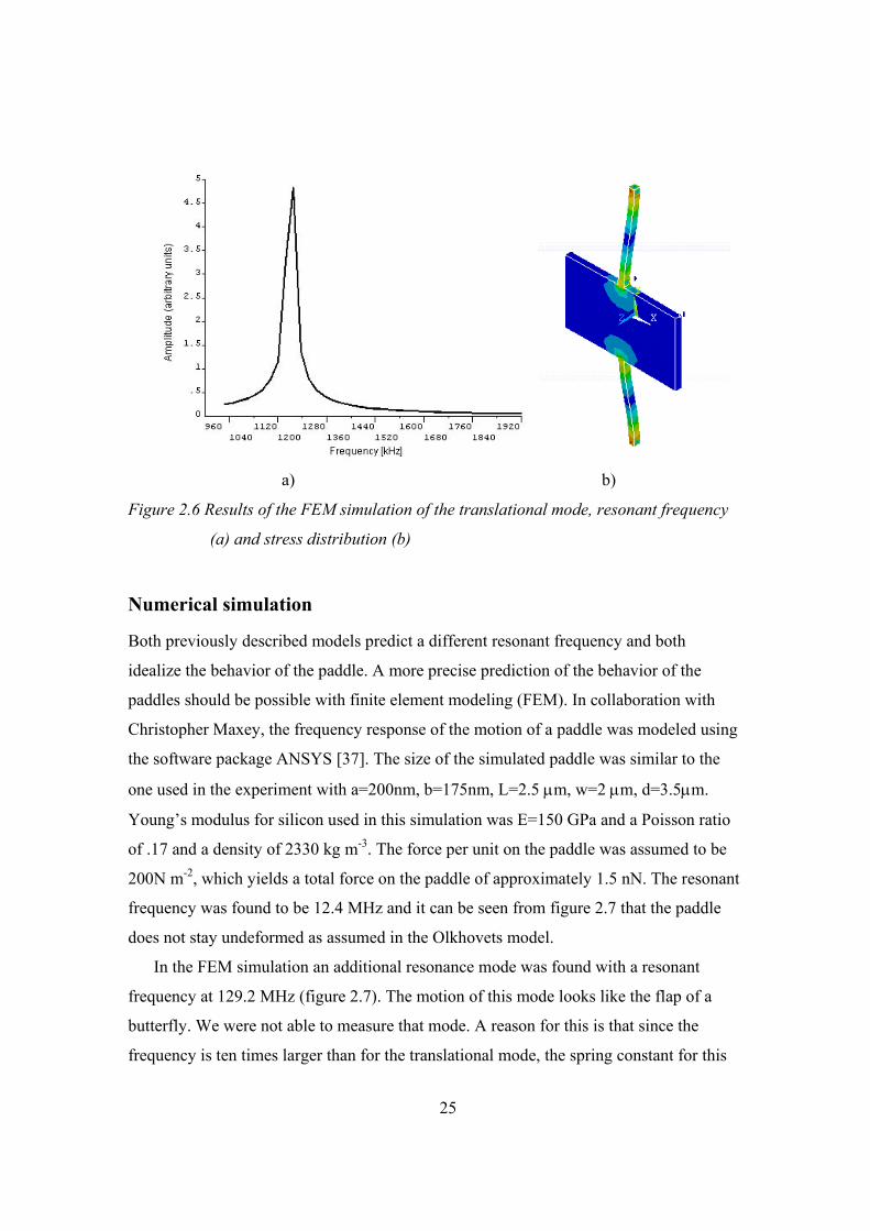
a) b)
Figure 2.6 Results of the FEM simulation of the translational mode, resonant frequency
(a) and stress distribution (b)
Numerical simulation
Both previously described models predict a different resonant frequency and both
idealize the behavior of the paddle. A more precise prediction of the behavior of the
paddles should be possible with finite element modeling (FEM). In collaboration with
Christopher Maxey, the frequency response of the motion of a paddle was modeled using
the software package ANSYS [37]. The size of the simulated paddle was similar to the
one used in the experiment with a=200nm, b=175nm, L=2.5 µm, w=2 µm, d=3.5µm.
Young’s modulus for silicon used in this simulation was E=150 GPa and a Poisson ratio
of .17 and a density of 2330 kg m-3. The force per unit on the paddle was assumed to be
200N m-2, which yields a total force on the paddle of approximately 1.5 nN. The resonant
frequency was found to be 12.4 MHz and it can be seen from figure 2.7 that the paddle
does not stay undeformed as assumed in the Olkhovets model.
In the FEM simulation an additional resonance mode was found with a resonant
frequency at 129.2 MHz (figure 2.7). The motion of this mode looks like the flap of a
butterfly. We were not able to measure that mode. A reason for this is that since the
frequency is ten times larger than for the translational mode, the spring constant for this
26
a) b)
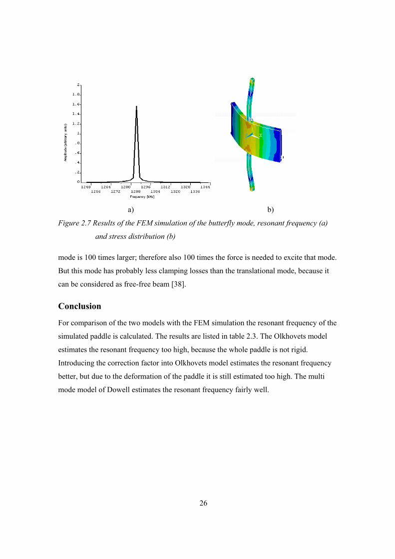
Figure 2.7 Results of the FEM simulation of the butterfly mode, resonant frequency (a)
and stress distribution (b)
mode is 100 times larger; therefore also 100 times the force is needed to excite that mode.
But this mode has probably less clamping losses than the translational mode, because it
can be considered as free-free beam [38].
Conclusion
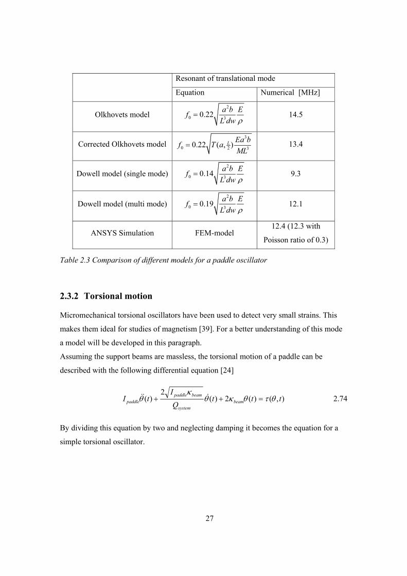
For comparison of the two models with the FEM simulation the resonant frequency of the
simulated paddle is calculated. The results are listed in table 2.3. The Olkhovets model
estimates the resonant frequency too high, because the whole paddle is not rigid.
Introducing the correction factor into Olkhovets model estimates the resonant frequency
better, but due to the deformation of the paddle it is still estimated too high. The multi
mode model of Dowell estimates the resonant frequency fairly well.
27
Resonant of translational mode
Equation Numerical [MHz]
Olkhovets model 2
0 30.22 a b EfL dw ρ
= 14.5
Corrected Olkhovets model 3
0 2 30.22 ( , )L Ea bf T aML
= 13.4
Dowell model (single mode) 2
0 30.14 a b EfL dw ρ
= 9.3
Dowell model (multi mode) 2
0 30.19 a b EfL dw ρ
= 12.1
ANSYS Simulation FEM-model 12.4 (12.3 with
Poisson ratio of 0.3)
Table 2.3 Comparison of different models for a paddle oscillator
2.3.2 Torsional motion
Micromechanical torsional oscillators have been used to detect very small strains. This
makes them ideal for studies of magnetism [39]. For a better understanding of this mode
a model will be developed in this paragraph.
Assuming the support beams are massless, the torsional motion of a paddle can be
described with the following differential equation [24]
),()(2)(2
)( tttQ
ItI beam
system
beampaddlepaddle θτθκθ
κθ =++ &&& 2.74
By dividing this equation by two and neglecting damping it becomes the equation for a
simple torsional oscillator.
28
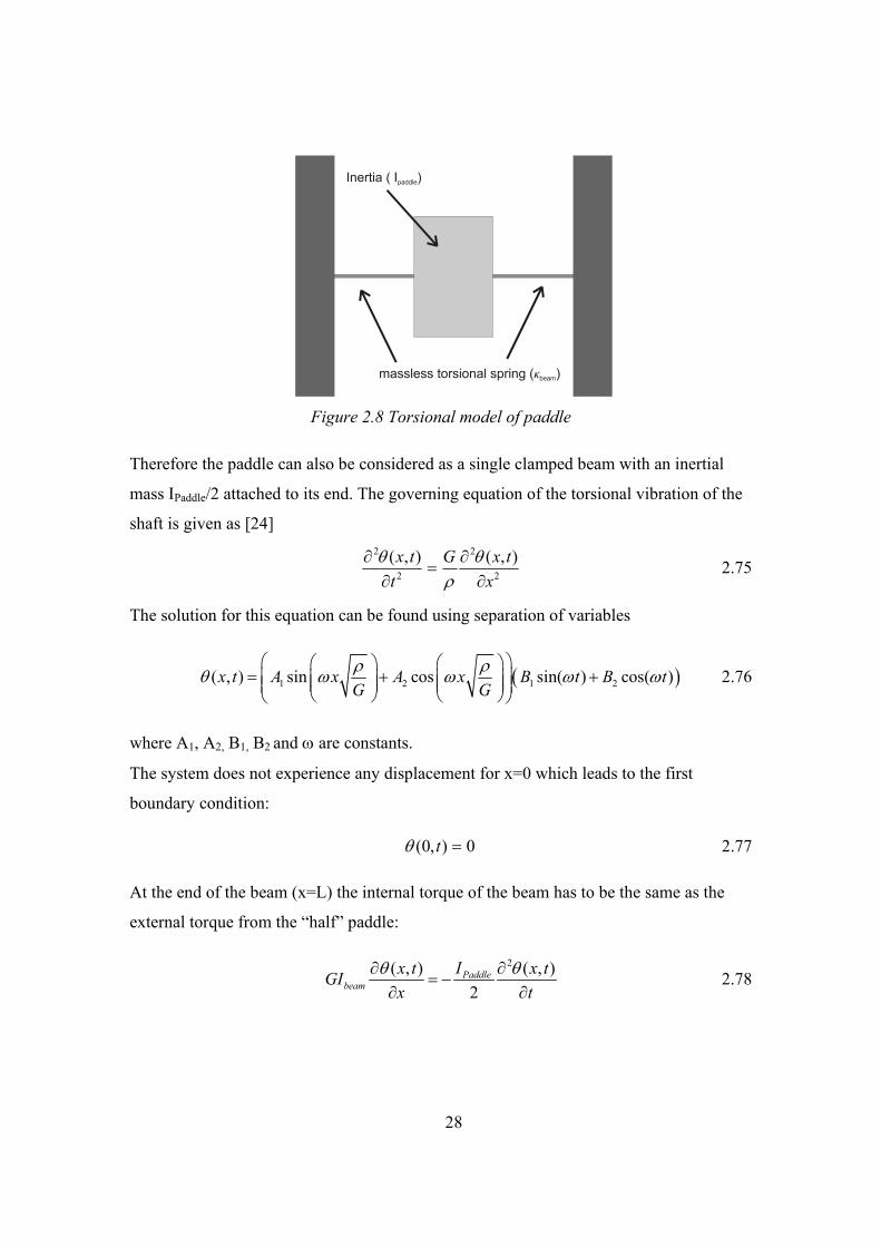
Figure 2.8 Torsional model of paddle
Therefore the paddle can also be considered as a single clamped beam with an inertial
mass IPaddle/2 attached to its end. The governing equation of the torsional vibration of the
shaft is given as [24]
2
2
2
2 ),(),(x
txGt
tx∂
∂=
∂∂ θ
ρθ 2.75
The solution for this equation can be found using separation of variables
( )1 2 1 2( , ) sin cos sin( ) cos( )x t A x A x B t B tG Gρ ρθ ω ω ω ω
= + +
2.76
where A1, A2, B1, B2 and ω are constants.
The system does not experience any displacement for x=0 which leads to the first
boundary condition:
0),0( =tθ 2.77
At the end of the beam (x=L) the internal torque of the beam has to be the same as the
external torque from the “half” paddle:
2( , ) ( , )
2Paddle
beamIx t x tGI
x tθ θ∂ ∂
= −∂ ∂
2.78
29
The first boundary condition leads directly to A2=0 and the second one to
Paddle
beam
ILI
cL
cL ρωω 2tan = 2.79
This equation has no analytical solution but can be solved numerical with the following
substitution
cLωβ = 2.80
Unlike for translational motion, it is not possible to find a general factor β that suits all
systems. Equation 2.79 has to be solved numerical for each system.
Other authors [34] [35] approximated the support beams of the paddle as simple beam
and found the following resonant frequency
GILab
baf
paddle
3
0 221
= β
π 2.81
where β(a/b) is a dimensionless function of the ratio a/b, with β(1.14)=0.16.
The moment of inertia for a symmetric paddle and a rectangular beam are given as [40]
2
2 22
12
Paddle
beam
dI dwa
a bI abL
ρ
ρ
=
+=
2.82
30
Resonant Frequency
Equation Symmetric
50 nm
asymmetric
Beam with intertial
mass
2tanPad
LIL LG G I
ρρ ρω ω
=
2.86 MHz 2.82 MHz
Simple beam 3
0 0.09paddle
abf GL I
= 3.34 MHz 3.28 MHz
Table 2.4 Comparison of the torsional resonant frequency of two different models with an
FEM simulation
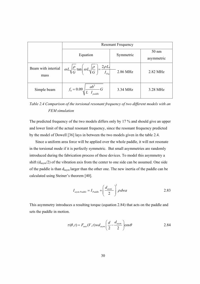
The predicted frequency of the two models differs only by 17 % and should give an upper
and lower limit of the actual resonant frequency, since the resonant frequency predicted
by the model of Dowell [36] lays in between the two models given in the table 2.4.
Since a uniform area force will be applied over the whole paddle, it will not resonate
in the torsional mode if it is perfectly symmetric. But small asymmetries are randomly
introduced during the fabrication process of these devices. To model this asymmetry a
shift (dasym/2) of the vibration axis from the center to one side can be assumed. One side
of the paddle is than dasym larger than the other one. The new inertia of the paddle can be
calculated using Steiner’s theorem [40].
2
2asym
asym Paddle Paddle
dI I dwaρ
= +
2.83
This asymmetry introduces a resulting torque (equation 2.84) that acts on the paddle and
sets the paddle in motion.
( , ) ( , ) cos2 2
asymunit asym
ddt F V t wdτ θ θ
= −
2.84
31
After the paddle is set in motion the gap dependency (h) of the force introduces an
additional torque and can be found as [35]
3
( , ) ( , )12unitwdt F V t
hτ θ θ≈ 2.85
Which leads to the following equation of motion
( )2 2 2
0
2
( , ) 2 cos( ) cos ( )
cos2 4 6
unit DC DC AC AC
asym asym
II F V t wd V V V t V tQ
d dd dd h
θ κθ θ ω ωω
θ θ
+ + = + +
+ +
&& &
2.86
With d >> dasym and an expansion for the cosines the equation can be rewritten as
( )2 2
2
0
( , ) 2 cos( ) ( 1 )2 2 6asym
unit DC DC AC
dI dI F V t wd V V V tQ h
θθ κθ θ ω θω
+ + = + − +
&& & 2.87
All higher order terms of the cosines expansion were neglected, as well as the
V2ACcos2(ωt) term. Further the damping and, since the deflection is small, nonlinear
terms were neglected, which reduces equation 2.87 to
( ) ( )2
2 2( , ) ( , )6 2
asymunit DC unit DC
ddI F V t wd V F V t wd Vh
θ κ θ
+ − =
&& 2.88
Which leads finally to a DC potential dependence of the resonant frequency
( ) 22
0
( , )1
6unit
DC
F V t wd df f V
hκ= − 2.89
32
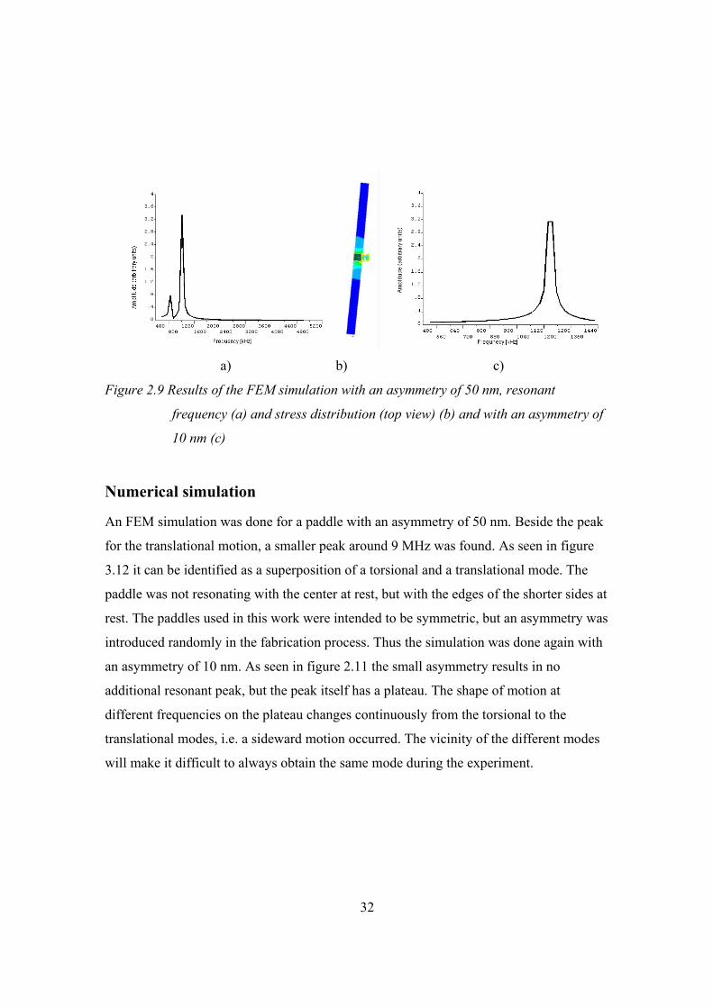
a) b) c)
Figure 2.9 Results of the FEM simulation with an asymmetry of 50 nm, resonant
frequency (a) and stress distribution (top view) (b) and with an asymmetry of
10 nm (c)
Numerical simulation
An FEM simulation was done for a paddle with an asymmetry of 50 nm. Beside the peak
for the translational motion, a smaller peak around 9 MHz was found. As seen in figure
3.12 it can be identified as a superposition of a torsional and a translational mode. The
paddle was not resonating with the center at rest, but with the edges of the shorter sides at
rest. The paddles used in this work were intended to be symmetric, but an asymmetry was
introduced randomly in the fabrication process. Thus the simulation was done again with
an asymmetry of 10 nm. As seen in figure 2.11 the small asymmetry results in no
additional resonant peak, but the peak itself has a plateau. The shape of motion at
different frequencies on the plateau changes continuously from the torsional to the
translational modes, i.e. a sideward motion occurred. The vicinity of the different modes
will make it difficult to always obtain the same mode during the experiment.
33
3 Loss mechanisms
For many applications resonators with high quality factor are needed. For filter
applications in wireless systems, it may be necessary to filter out a weak signal in the
vicinity of a strong interfering signal. Since the output signal of a filter is proportional to
the amplitude of the resonator, the signal of interest may still be superposed with the
interfering signal of the same magnitude if a resonator with a low quality factor is used.
High quality factors are therefore needed to reduce the interfering signal. For sensor
applications, the shift of the resonance frequency can be determined more precisely if the
resonator has a higher quality factor, leading to greater sensitivity. No NEMS resonator
with a higher quality factor than 107 have been reported [17]; most NEMS do not even
come close to this value. In macroscopic resonators much higher Q-factors can be
obtained. Therefore the origin of losses in NEM resonators must be understood in order
to increase the quality factor.
The loss mechanisms described in part 3.2 (air damping) and 3.3 (clamping losses)
are extrinsic loss mechanisms: they have nothing to do with the material itself but are
influenced by the design of the structure. The loss mechanisms discussed in paragraph
3.4 to 3.6 are intrinsic loss mechanisms that will limit the highest possible achievable Q-
factor. Paragraph 3.7 discusses surface related loss mechanisms. In addition loss
mechanism associated with stress relaxation will be discussed in the next chapter.
Most of the theoretical and experimental work on energy dissipation was done with
large oscillators at low frequencies (~1 Hz), which makes it questionable whether the
theoretical description of the loss mechanism can be easily applied to high frequency
NEMS.
34
3.1 Energy dissipation and quality factor
The extent of the energy dissipation is often expressed in the form of a quality factor
[41]. The quality factor Q is defined as
1 1 Energy loss per cycle2 Total elastic energyQ π
= 3.1
This can easily be seen for an oscillator with coulomb damping ( ˆ E = E(1 + iη)).
Assuming the applied external stress has the following form
σ = σ 0eiωt 3.2
The strain response will then have a phase shift
ε = ε0eiωt +φ 3.3
due to the complex part of the modulus. The elastic energy stored in the oscillator is
W =12
Eσ02 3.4
The energy that is dissipated per cycle is
∆W = πEησ02 3.5
which then gives us
1Q
=∆W
2πW= tanφ = η 3.6
The energy dissipation can also be expressed in the form of a complex resonant
frequency [42]. The real part gives the resonant frequency and the imaginary part the
damping. The mechanical energy is proportional to the square of its amplitude, the
inverse of the quality factor can therefore be written as
( )
1 Im( )2ReQ
ωω
= 3.7
35
In general, different energy dissipation mechanisms contribute to the quality factor. An
individual quality factor can be assigned to the different mechanisms. The overall Q-
factor of a system can then be found as the sum of the inverses of the individual Q-factors
1 1
tot iQ Q= ∑ 3.8
3.2 Air friction
Air damping can be separated into an intrinsic, a molecular, and a viscous region. In the
intrinsic region, air friction is not a significant source of energy loss. In general, the
interaction of the surroundings with the beam can be summarized with a drag force Fdrag
[43]. The drag force has the following form
( ) 2 21 2 1 1drag x x x x x
LF i u u u Lu uβ γβ β β γω ω
= + = − = −& & & & & 3.9
where xu& is the velocity and L the length of the beam. It can be shown that γ1 is
proportional to the quality factor and γ2 is proportional to the frequency shift.
3.2.1 Viscous region
For higher pressure, in the viscous region the gas acts as a viscous fluid [43]. Assuming
that the air is incompressible and that the Reynolds number is small (no turbulences) the
force on the surface can be calculated using the Navier-Stokes and the continuity
equation. The beam will be approximated with a row of spheres vibrating independently
of each other, because it is difficult to determine the velocity field of the air around the
vibrating beam. The force on the surface is then given as
32 96 1 13 2drag gas
rF r i r vrδπµ π ρ ω
δ = + − +
3.10
36
where µ the dynamic viscosity of the medium and ρ0 the density of the gas, which for an
ideal gas is:
0M pRT
ρ = 3.11
δ is the region around the beam where the motion of the gas is turbulent and is
approximately:
1/ 2
0
2µδρ ω
=
3.12
From the drag force it is easy to obtain the Q-factor and the frequency shift.
( )0 0
1 6 1beam beam
r
A wtlQr γ
ρ ρω ωγ πµ
= =+
3.13
3
02
0
1 912 3 2beam beam
rA lwt r
π ργω δω ρ ρ∆ = − = − +
3.14
For the calculation, the radius r can be approximated with the width of the beam.
3.2.2 Molecular region
At low pressure the collisions of the air molecules with the resonator surface can be
considered independent of each other [43]. The force on the resonator is due to these
collisions. The damping parameter γ1 is proportional to the air pressure p and the width of
the beam w
12
1
2
329
0
M wpRT
γπ
γ
=
=
3.15
37
where R is the gas constant and M the mass of the gas molecules (Mair ≈ 29 g/mol). The
quality factor is then simply
1/ 2
0 0932
beam beamA tRTQM p
ρ ω ρ ωπγ
= =
3.16
where ρ is the density of the beam material.
Blom et al [43] found the transition from the viscous to the molecular regime around one
torr and from molecular to the intrinsic regime between 10-2 and 10-3 torr for a cantilever
with a cross section in the mm2 range.
3.2.3 Squeeze force
If the gap (h0) between the beam and the supporting surface is small a squeeze force acts
between the beam and the surface [44]. This force can be calculated using the Reynholds
equation. The Q-factor can be found as
0
3
02beamh t
Qw
ρω
µ= 3.17
This approximation holds if the beam is much longer than it is wide, and if the initial gap
is uniform and the vibration is much smaller than the gap.
It is assumed that the pressure is constant around the resonator, which might not be
true, since the pumping effect resulting from the vibration might introduce an
inhomogeneous pressure distribution underneath the resonator [45]. In an experimental
setup, we therefore must consider that the small size of the gap between the resonator and
the substrate reduces the effective pumping speed underneath the resonator. The pressure
underneath the resonator is therefore probably higher than on the top of the resonator.
38
3.3 Clamping
Since real elements are never perfectly rigid, energy can be dissipated from the resonator
to the support structure, where local deformations and microslip can occur. The rhodium
structures of chapter seven can be considered as a beam fixed at one end by a rigid clamp.
At the contact area between the beam and the clamp, slip occurs if the beam bends. The
energy loss per cycle is proportional to the inverse of the friction force at the contact area.
Increasing the pressure on the beam therefore reduces the energy losses [46]. It is often
not possible to increase the rigidity of the support, but energy losses can be reduced with
an optimized design. Olkhovets [43] showed that a double beam with a flexible support
improves the Q factor approximately 30 % compared to a cantilever (figure 3.1).
Figure 3.1 Designs to reduce clamping loss by Olkhovets
Wang et al [38] created a “free-free” beam with four torsional supports beam, each with a
length of a quarter of the resonant frequency of the free-free beam. Since as a result of
this design the torsional beams do not move at their support, no energy is dissipated into
the support structure. The Roukes group [47] used a torsional double resonator to
decouple the center resonator from its support.
39
3.4 Phonon-Phonon Scattering
Phonon-phonon scattering takes place if the oscillatory wavelength is considerably larger
than the mean free path of phonons. The photons due to the oscillation (sound-waves) of
the structure can interact with the phonons due to thermal vibration [47]. These sound-
waves locally change the thermal-phonon frequencies and energy is dissipated to restore
the equilibrium. The values for ωQ are found to be in the order of 1012 to 1014 for
aluminum at 4.2 K and room temperature respectively. This process is an intrinsic
process that will limit the largest possible Q-factor.
3.5 Phonon-Electron Scattering
In metals a free electron gas is present. Due to the external periodical force the ions start
to oscillate which produces a varying electric field. The oscillating electric field forces
the electrons to move. An electron gas can be approximated as a viscous fluid [47],
therefore energy is dissipated by the motion of the electrons. For aluminum the ωQ is
found to be 3 x 10¹¹ for 4.2 K and 5 x 10¹³ for 4.2 K. However, an intrinsic
semiconductor at room temperature has electrons and holes through thermal excitation.
The external strain can change the band structure so that electron can migrate from one
band to another. When an electron jumps from one band to another energy is dissipated.
As with photon-photon scattering, electron-photon scattering is also a Q-factor limiting
process.
3.6 High temperature background
In experiments, it is observed that at a transition temperature, the damping curve raises
continually to a very large value until the melting point of the material is reached. This
high temperature background is much smaller for single crystals than for polycrystals and
it is smaller for samples with larger grains. This background might be due to a coupled
relaxation behavior where stress relaxation across viscous slip bands takes place. The
shorter slip bands relax first and as the longer ones start to relax additional stress can be
put on the shorter bands.
40
3.7 Surface related effects
Carr [25] observed a linear relationship between the damping and the surface-volume
ratio. Yasumura et al stated in a literature review that the Q-factor decreased with
decreasing oscillator dimensions [58]. This suggests that the dominant loss mechanisms
are surface related in NEM resonators. Unfortunately, loss mechanisms at the surface are
still not well understood. A few possible mechanisms are proposed here.
3.7.1 Thin film on surface
Pohl’s group [59] developed a method to obtain the quality factor of a thin film by
depositing a film on a centimeter scale silicon double oscillator, and then measuring the
Q-factors of the oscillator with and without the film. The relationship between the Q-
factors is given as
1 1 1 13 3
Si Si Si Si
film Film Film Paddle and Film Paddle Film Film
G t G tQ G t Q Q G t Q
= − = ∆
3.18
where GFilm and GSi are the rigidity modulus and tfilm and tSi the thickness of the
deposited material and Silicon respectively. All their measurements were taken at low
temperatures (T < 2K). They found that the Q-factor of the film is similar to the one in
bulk material. But they observed that the Q-factor of a SiO2 film already differs
significantly from the bulk at 10 K. The results suggest that for higher temperature, a
more complex interaction between the two layers takes place and increases the losses.
3.7.2 Metal layer
To increase the conductivity of the resonator, a thin metal layer is deposited on the
resonator. Evoy et al [34] [60] found that the quality factor decreases linearly with the
thickness of this metal layer. From equation 3.18 it can be seen that this is expected:
31 1 1Film Film
Paddle and Film Si Si film Paddle
G tQ G t Q Q
= + 3.19
But there is no dependence of the surface-volume ratio so it cannot explain the
dependence of the Q-factor on the surface-volume ratio.
41
3.7.3 Oxide layer
A thin amorphous layer of oxide is formed if a silicon device is exposed to air. The layer
is approximately 2.5 nm thick [25]. Since SiO2 needs twice the space that silicon does,
additional stress is created at the interface, which results in additional thermoelastic
losses (paragraph 4.2). Removing the SiO2 and all surface contamination by heat
treatment increases the Q-factor by almost a factor of 5 [61]. Terminating the surface
with hydrogen further increases the Q-factor. The hydrogen reduces the stress on the
surface. If the thickness of the resonator is 200 nm, as in our experiments, the ratio of the
film thickness and the resonator is tfilm/tsub ≈ 10-2. For this ratio of a SiO2 layer with the
substrate the Q-factor of the system decreased by around ∆Q≈105 compared to the paddle
without a SiO2 layer [59]. From equation 3.18 we see that
1 1 1
Paddle and Film PaddleQ Q Q= +
∆ 3.20
The Q-factor of a 200 nm thick resonator to 105 at 1.3 K. In quartz glass (SiO2) it is
assumed that the Si-O bond length changes if an external stress is applied. The
longitudinal oscillation of the bridging oxygen atom, resulting from an oscillating stress,
dissipates energy [41]. Since the oxide layers on silicon NEM resonators also contain Si-
O bonds, this process can also take place there.
3.7.4 Water layer
On a silicon surface with its native SiO2 layer, a water layer of around 10 nm can be
found (in normal atmosphere) [79]. Since water increases the internal friction of glass
(SiO2) by forming vibrating Si-OH groups [78], it is most likely that it also increases the
losses in silicon NEM resonators.
42
3.8 Summary
Since photon-photon scattering and photon-electron scattering related losses are very
small and NEM resonators have a relatively low quality factor, this effect can be
neglected in NEM resonators. Air friction can easily be limited by performing the
experiments in a good enough vacuum (p<< 1 mtorr). The influence of clamping losses in
silicon resonators is highly controversial. Since the rhodium NEM resonator is clamped
to the bonding pad, it is expected that clamping losses contribute much more to the total
energy dissipation than in silicon NEM resonators. The structures used in this work have
a high surface-volume ratio, therefore it is expected that surface related loss mechanisms
are dominant [33] [58].
43
4 Stress relaxation
Energy dissipation is a strong function of temperature. At different temperatures different
mechanisms can be dominant. Most mechanisms show a dissipation peak with a specific
activation energy and relaxation time. This process is also called Debye relaxation. Since
a relaxation time and an activation energy can be attributed to each relaxation
mechanism, it is possible to compare the dominant loss mechanisms between different
resonators. This helps to understand and isolate the dominant loss mechanism of an NEM
resonator.
Relaxation results from a transition between two configurations in a solid. In a
resonator the transition is stress induced. This behavior can be illustrated by considering
two states in a system with slightly different energy levels, separated by a potential
barrier of height H. Before a stress is applied, the system is in its minimum energy state.
If an external stress is applied to the system the energy levels change their position
(figure 4.1), and the other state is energetically more favorable. If the system can
overcome the energy barrier H a transition from state one to state two takes place. The
system is relaxed and the energy difference between the two states is lost.
In this chapter relaxation will first be explained mathematically (4.1) and then
different relaxation phenomena (4.2 to 4.4) will be discussed.
44
Figure 4.1 Influence of an applied stress to the energy levels of a system
4.1 Mathematical description of relaxation
To understand the relaxation behaviour of a material, a model needs to be found that
describes its properties. Rheological models are a helpful tool to do so. They are the
equivalent in elasticity to what equivalent circuit diagrams are in electrical engineering.
[48].
In rheological models three elements are used: Hook’s elements to describe elastic
behaviour (figure 4.2a), Newton’s elements to describe viscous damping (figure 4.2b),
and St. Venant element for coulomb damping (figure 4.2c). The different elements can be
connected either parallel to each other, then the strain is equal in both elements, or in
series, then the stress in the two elements is equal.
The materials used in this work have a viscoelastic behavior. The simplest model to
describe their stress relaxation and their creep behavior correctly is the Zener model. It
consists of a Hook's element parallel to a Newton's element and an additional Hook’s
element in series. The stress strain relationship for this model is then
( ) ( )( ) ( )s p p dd
s p s p s p
E E Ed t d tt tE E dt E E E E dt
ηη σ εσ ε+ = ++ + +
4.1
45
a) b) c) d)
Ep
Es
d
Figure 4.2 Hook’s element (a), Newton’s element (b), St. Venenat element (c) and the
rheological representations of the Zener model (d)
From equation 4.1 the origin of the dissipation peaks can be explained. The following
derivation is a summary of the one given in reference 49. For simplification the
prefactors of equation 4.1are replaced by single constants.
( ) ( )( ) ( )d t d ta t b c t ddt dtσ εσ ε+ = + 4.2
To give some meaning to the constants in equation 4.2 in terms of relaxation two simple
cases are considered: relaxation and creep. If a constant strain ε0 is applied to a solid at
time t=0, the stress-strain relationship (equation 4.2) becomes
aσ (t) + bdσ (t)
dt= cε0 4.3
and has the following solution
σ(t) =caε0 + σ0 −
caε0
e
− ab
t 4.4
The stress reaches its equilibrium at σ=c/a ε0. Therefore, a relaxed Young’s modulus
ER=c/a can be introduced. Furthermore, a relaxation time τσ = b/a can be introduced. At
t=τσ the stress is reduced to 36 % of its original value. If a constant stress σ0 at t=0 is
applied to the system, the stress-strain relationship becomes
dt
tdcdEtE RR
)()(0εεσ += 4.5
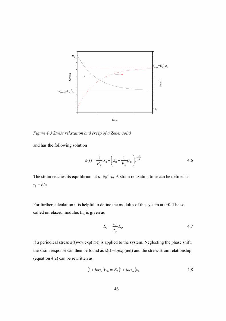
46
εrelex=ER-1 σ0
ε0
σ0
σrelaxed=ER-1ε0
time
Stre
ss
Stra
in
Figure 4.3 Stress relaxation and creep of a Zener solid
and has the following solution
0 0 01 1( )
c td
R R
t eE E
ε σ ε σ−
= + −
4.6
The strain reaches its equilibrium at ε=ER-1σ0. A strain relaxation time can be defined as
τε = d/c.
For further calculation it is helpful to define the modulus of the system at t=0. The so
called unrelaxed modulus Eu, is given as
Ru EEε
σ
ττ
= 4.7
if a periodical stress σ(t)=σ0 exp(iωt) is applied to the system. Neglecting the phase shift,
the strain response can then be found as ε(t) =ε0exp(iωt) and the stress-strain relationship
(equation 4.2) can be rewritten as
( ) ( ) 00 11 εωτσωτ σε iEi R +=+ 4.8
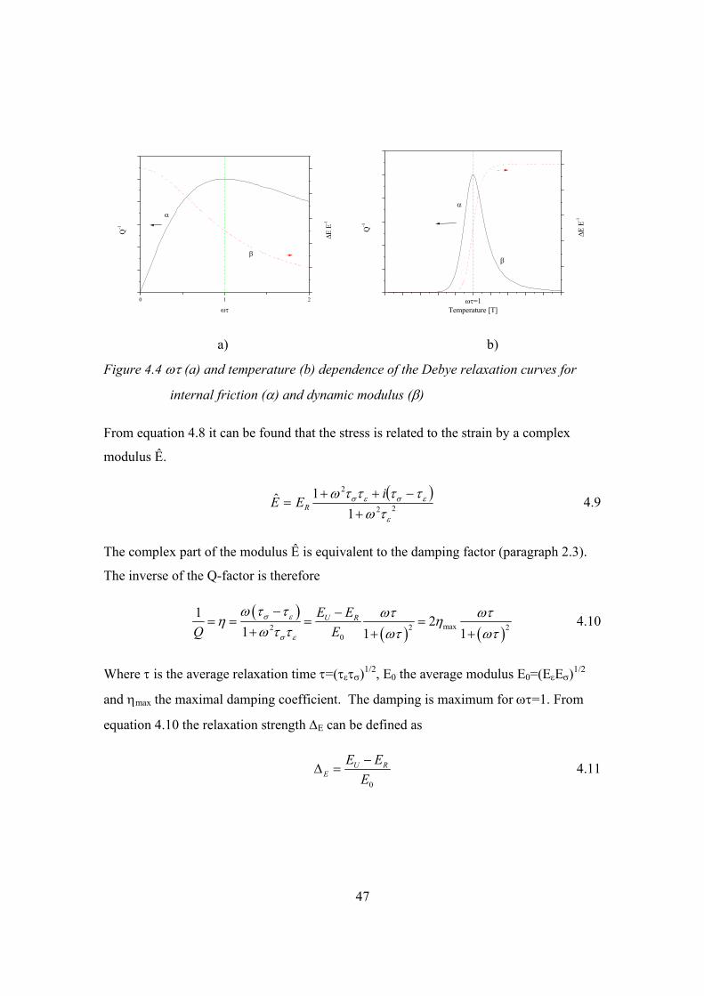
47
0 1 2
α
ωτ
Q-1
β
∆E
E-1
α
ωτ=1
Temperature [T]
Q-1
β
∆E
E-1
a) b)
Figure 4.4 ωτ (a) and temperature (b) dependence of the Debye relaxation curves for
internal friction (α) and dynamic modulus (β)
From equation 4.8 it can be found that the stress is related to the strain by a complex
modulus Ê.
( )22
2
11ˆ
ε
εσεσ
τωττττω
+−++
=iEE R 4.9
The complex part of the modulus Ê is equivalent to the damping factor (paragraph 2.3).
The inverse of the Q-factor is therefore
( )( ) ( )max2 22
0
1 21 1 1
U RE EQ E
σ ε
σ ε
ω τ τ ωτ ωτη ηω τ τ ωτ ωτ
− −= = = =
+ + + 4.10
Where τ is the average relaxation time τ=(τετσ)1/2, E0 the average modulus E0=(EεEσ)1/2
and ηmax the maximal damping coefficient. The damping is maximum for ωτ=1. From
equation 4.10 the relaxation strength ∆E can be defined as
0
U RE
E EE−
∆ = 4.11
48
The real part of the modulus (Ê) depends also on the frequency and on the strain
relaxation time.
( ) ( ) ( ) ( )
2
max2 2 2 2
1 121 1 1 1
T S U R U RR U U
S S
E E E EE E E Eω τ τ ηωτ ωτ ωτ ωτ
+ − −= = − ≈ − =
+ + + + 4.12
In an experimental setting with measurements over a wide range of ωτ, τS can be
approximated with τ (τS≈τ). The change of the modulus is then
( )212
1M
EE
ηωτ
∆=
+ 4.13
For most relaxation phenomena the relaxation time is an exponential function of the
temperature and can be described with an Arrhenius-type equation
0( )HkTT eτ τ= 4.14
H is the activation energy, any temperature dependence of H can be incorporated into τ0.
The dissipation peak at ωτ=1 can be understood quantitatively in the following way
[42]: If the vibration period is much larger than the relaxation time (ω<<1/τ), the system
stays almost exclusively in equilibrium and not much energy is dissipated. If the period is
much smaller than the relaxation time (ω>>1/τ), the system then does not have any time
to relax and again not much energy is dissipated.
In real materials a deviation of the relaxation peak from the symmetric Debye peak
can often be observed. This is either due to a distribution of relaxation times for one
relaxation mechanism or to different relaxation phenomena lying close together and
overlapping each other. A distribution of relaxation times can result from
inhomogeneities in the material or from a different stress in the center than on the
surface.
49
4.2 Thermoelastic relaxation
If the resonator is deformed, different areas experience different strains. Since stress and
strain are coupled with temperature and entropy, the beam will then have a non uniform
temperature distribution. Heat will flow from the high temperature regions to the low
temperature regions and thus energy will be dissipated. Torsional modes do not suffer
volume change and therefore no thermoelastic damping takes place [50]. Thermoelastic
relaxation was first predicted and confirmed experimentally by Zener in 1937 and 38 [51]
[52] [53]. Based on this work, Lifshitz developed a more accurate model to predict
thermoelastic relaxation for a rectangular Euler-Bernoulli beam [42]. The following
derivation follows reference [42]. The same coordinate system is used as introduced in
paragraph 2.1. In consideration of thermal expansion the normal stresses in the beam are
given by
1z z T
Eε σ α= + ∆ 4.15
and the stresses in the other directions are
x y x TEµε ε σ α= = − + ∆ 4.16
where µ is the Poisson ratio and α the thermal expansion coefficient. All shear stresses
are assumed to be zero. Following the same steps as in paragraph 2.1 the equation of
motion can be obtained
2 2
2 2 2 0x zy T
u uA EI E It z z
ρ α ∂ ∂∂
+ + = ∂ ∂ ∂ 4.17
where IT is the thermal inertia that can be defined as
TA
I x Tdxdy= ∆∫ 4.18
50
The heat equation in the presence of thermoelastic coupling in y-direction is given as
2 2
2 2
11 21 2
EE th
T T uD yt x t x
µµ α
∆+ ∂∆ ∂ ∆ ∂ ∂+ ∆ = + − ∂ ∂ ∂ ∂
4.19
where ∆E is the relaxation strength:
2
0E
P
E TCα
∆ = 4.20
CP is the heat capacity per unit volume at constant pressure. Assuming that the heat
transfer is fast enough such that the temperature changes follows the displacement
without a time delay, the frequency can be found as
0 1 [1 ( )]E fω ω ω= + ∆ + 4.21
Where ω0 is the resonant frequency for a beam without thermoelastic losses (equation
2.28) and f (ω) is
3 3
24( ) tan2 2tk tkf
t kω = −
4.22
with k
( )12 Th
k iDω
= + 4.23
where t is the thickness of the beam and the DTh is the temperature dependent diffusion
constant
HkT
th oD D e−
= 4.24
Using a square root extension and neglecting all higher order terms the dispersion
relation becomes
0 1 [1 ( )]2
E fω ω ω∆ = + + 4.25
51
and the Q factor can be found as
2
02 3
1 Im( ) 6 6 sinh sin2Re( ) cosh cos
E TQ C
αω ξ ξω ξ ξ ξ ξ
+= = − +
4.26
with
0
2 Th
tDωξ = 4.27
We see a strong dependence of the quality factor on the thickness of the beam. The
thermoelastic relaxation peak can be seen more direct from Zener’s original work, where
he started from equation 4.1 and found the Q-factor for a rectangular beam as:
2
02 2 2 2
11 1
adE E E TQ E cσ
αωτ ωτω τ ω τ
−≈ =
+ + 4.28
with
thD
a2
2
πτ = 4.29
Cavities and other impurities or grains with different crystal orientations introduce a non-
uniform stress distribution even if no external stress is applied. This non-uniform stress
distribution increases thermoelastic losses. A mathematical proof would be beyond the
scope of this thesis but is given by Zener [52]. The concept of thermoelastic losses fails if
the length of the beam is smaller than the mean free path of a thermal photon. [54]
4.3 Defect Relaxation
Point defects in crystals produce a local non-uniform stress distribution [50]. It is possible
to associate a symmetry with each defect. If the defect symmetry is lower than the crystal
symmetry, an elastic dipole originates. Consequently, there will be an interaction between
the dipole and a homogeneous applied stress and if an activation energy is overcome, a
reordering of the dipoles take place.
52
In bcc metals, the dipole is introduced by interstitial impurities (Snoek relaxation)
[50]. The interstitial atoms occupy the octahedral sites and have a four-fold symmetry
(tetragonal symmetry). When a dipole reorientates the interstitials jump to the
neighboring octahedral site. It can be found that the activation energy that controls the
relaxation time is similar to the one for the migration of the interstitials.
Zener relaxation is observed in over 20 alloy systems and in all three common
metallic structures [50]. The relaxation is due to a stress-introduced reorientation of
atom-defect pairs in the nearest neighbor configuration. The atom-defect pair can be
considered as a dumbbell that rotates about its center. The concept of defect pairs applies
only to solids with a high impurity concentration. In silver the peak starts to be become
visible at a zinc impurity of about 3.7 % and increases significantly with zinc
concentration.
The simplest model to describe dislocation relaxation is to consider the dislocation as
a loop that is firmly pinned at its end and executes vibration under an external periodical
stress (like a vibrating string) [50]. A major limitation of this model is that stresses and
strains outside the slip plane are neglected. The pinning points are assumed fixed, which
is only true at low temperatures, where the diffusion is negligible. Dislocation damping
can be nonlinear and shows a strong amplitude dependence.
4.4 Grain boundary relaxation
In a polycrystalline material the grains slide back and forth if a periodical stress is
applied. Since friction occurs if two grains are sliding along each other, energy is
dissipated [55]. The sliding is blocked at the end of the grain but can be continued if the
strain is large enough to overcome the blocking. The activation energy of grain boundary
relaxation lies between the activation energy of volume diffusion and of grain boundary
diffusion, which suggests that boundary relaxation is linked to diffusion. The grain
boundary consists of many disordered atom groups, separated by regions where the atoms
fit (figure 4.5).
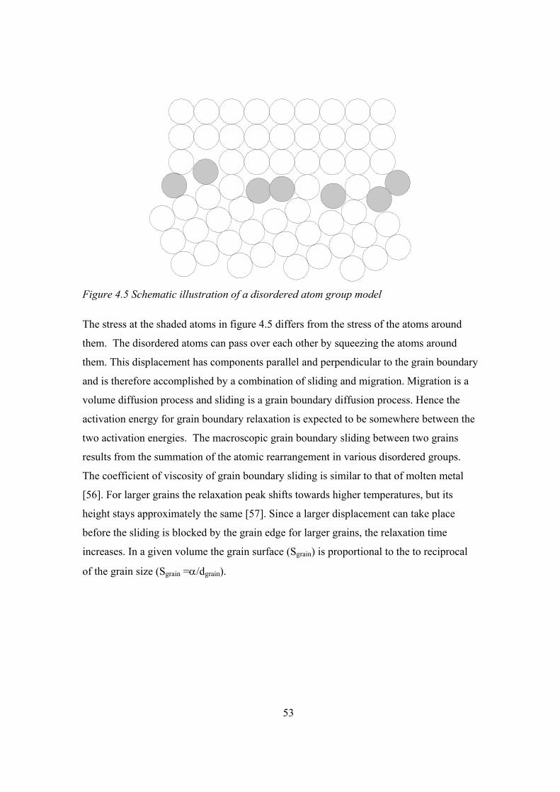
53
Figure 4.5 Schematic illustration of a disordered atom group model
The stress at the shaded atoms in figure 4.5 differs from the stress of the atoms around
them. The disordered atoms can pass over each other by squeezing the atoms around
them. This displacement has components parallel and perpendicular to the grain boundary
and is therefore accomplished by a combination of sliding and migration. Migration is a
volume diffusion process and sliding is a grain boundary diffusion process. Hence the
activation energy for grain boundary relaxation is expected to be somewhere between the
two activation energies. The macroscopic grain boundary sliding between two grains
results from the summation of the atomic rearrangement in various disordered groups.
The coefficient of viscosity of grain boundary sliding is similar to that of molten metal
[56]. For larger grains the relaxation peak shifts towards higher temperatures, but its
height stays approximately the same [57]. Since a larger displacement can take place
before the sliding is blocked by the grain edge for larger grains, the relaxation time
increases. In a given volume the grain surface (Sgrain) is proportional to the to reciprocal
of the grain size (Sgrain =α/dgrain).
54
The energy dissipation for each grain (Egrain ) is proportional to the displacement at the
grain boundary and the maximum displacement is proportional to the grain size (Egrain=β
dgrain). The total dissipated energy (∆E) in a given volume is then
grain grainE E S αβ∆ = = 4.30
where α and β are constant. From equation 4.30 it can be seen that the total dissipated
energy is independent of the grain size.
4.5 Summary
Thermoelastic and defect related losses will be present in NEM resonators, but it is
expected that they are not dominant and do not show a relaxation peak in the temperature
range available in this work [33]. Grain boundary related losses play an important role in
the rhodium samples. Since grain boundary peaks are at higher temperatures [55]-[57] it
is not possible to investigate grain boundary relaxation in this work.
55
5 Device fabrication and setup
The fabrication of NEMS involves electron beam lithography (EBL), metal deposition,
RIE and wet etch processes. This project involved the installation of an EBL system at
Virginia Tech. Once the EBL tool was installed and preliminary pattern had been written,
the NEMS fabrication process originally developed at Cornell [65] [25] was optimized
for the equipment available at Virginia Tech by William Barnhart [64].
The characterization of NEM resonators requires an experimental test bed offering
sub-nanometer deflection detection sensitivity. Since no commercial system is available,
this project also involved the building of such a system. Paragraph 1.4 will outline
different detection methods, and will justify our choice of the specific technique chosen
for this work.
5.1 Electron beam lithography
In electron beam lithography (EBL), a beam of electrons is scanned across a resist-
covered surface [62]. The electrons change the chemical structure of the resist. In positive
resists, the electrons break the polymer chains of the resist. After developing, the exposed
parts are dissolved, while the rest of the resist stays on the surface. In a negative resist,
however, the polymer chains are cross-linked by the electrons. In this case, the exposed
resist remains therefore on the surface, while the unexposed is dissolved in the
developing solution.
Since the wavelength associated with electrons is much smaller than those of photons
(2 Å for electrons with an energy of 30 keV), the exposure resolution is no longer limited
56
by diffraction as in optical lithography, but rather by electron scattering events in the
resist. For instance, PMMA has an intrinsic resolution limit of 10nm.
Quick turnaround times and the ability to write patterns in the submicron region
makes EBL a very versatile tool that is widely employed in research and development. It
is also commonly employed for the fabrication of masks for optical lithography systems.
5.1.1 Electron-Solid-Interaction
When the electrons interact with the resist, they get scattered [62]. Small angle
scattering events, also known as forward scattering, results in an enlargement of the beam
diameter. The enlargement of the beam is empirically found as
Resist
acceleration
0.9V
td∆ = 5.1
where tresist is the resist thickness in nanometers and Vaccelration the beam voltage in
kilovolts. Using the highest available acceleration voltage and the thinnest possible resist
increases the resolution of the lithography. The thickness of the resist cannot be reduced
arbitrarily, because the steps following the lithography need a certain resist thickness (i.e.
the resist must be thicker than the metal layer that is deposited in the next step). Electrons
also undergo large angle scattering, also known as backscattering. This happens
especially in the substrate due to its higher density compared with the resist.
Backscattered electrons result in an exposure of the resist from its rear, therefore an
adjustment of the dose is required to prevent overexposure. This effect is called the
proximity effect. The fraction of electrons that backscatter is roughly independent of the
beam energy but depends strongly on the substrate material. The percentage of
backscattered electrons ranges from 17% for silicon to 50% in tungsten. Finally, when
the electrons slow down, a cascade of low voltage secondary electrons is created.
Secondary electrons have energy between 2 and 50 eV. They do the bulk of the exposure,
but also widen the beam by roughly 10 nm. Figure 5.1 is a simulation of the scattering of
the electrons and shows how the acceleration voltage affects the EBL resolution.
57
5.1.2 Strategy to avoid the proximity effect
The interaction between the resist and the electron can be simulated prior to writing. The
dose can then be adjusted for each part of the pattern so that the whole structure is
exposed equally with the same dose. The required calculations are complex and time-
consuming. A correction method where no calculation is required is the GHOST method.
Here the inverse shade of the pattern is written with a defocused beam to imitate
backscattering for the areas that experience less backscattering. After the structure is
written the whole writing field was exposed to the same background dose. Expensive
stand alone EBL systems have either dose modulation or GHOST built in, while in low
cost systems the proximity effect can only be corrected manually, by assigning different
doses to different parts.
Another approach to reduce proximity effect is to use a multilayer resist where a first
thin layer is sensitive to electrons, while the second thicker layer is not. The thick layer
absorbs all backscattered electrons, so that they cannot damage the top layer. The pattern
from the thin layer is transferred into the thicker layer using a dry etching process.
5.2 Virginia Tech EBL system
The system installed at Viginia Tech is the Nanometer Pattern Generation System
(NPGS) from J. C. Nabity Lithography Systems. This pattern generator was installed as
an add-on module to a pre-existing LEO 1550 SEM. This system is based on a Windows
PC with a data translation DT2823 multifunction board (DAC). The board is used to
generate the X and Y beam deflection [62]. NPGS controls the stage and other
microscope settings via the serial port. The ISA-bus limits the deflection speed to around
100 kHz, which is equivalent to a minimum dwell time of 10 µs per point. The NPGS
uses a vector scan method, where the view field is sectioned in single pixels. Each shape
is filled by rastering the beam along the pattern. A limitation of this SEM based system is
the absence of a high tech laser stage, which reduces the maximum structure size to the
view field. Due to the size of our structures this is not a problem.
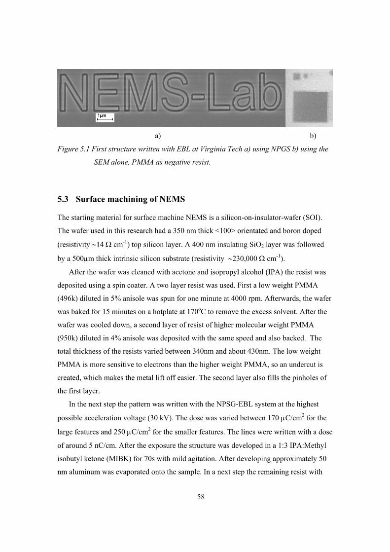
58
a) b)
Figure 5.1 First structure written with EBL at Virginia Tech a) using NPGS b) using the
SEM alone, PMMA as negative resist.
5.3 Surface machining of NEMS
The starting material for surface machine NEMS is a silicon-on-insulator-wafer (SOI).
The wafer used in this research had a 350 nm thick <100> orientated and boron doped
(resistivity ∼14 Ω cm-1) top silicon layer. A 400 nm insulating SiO2 layer was followed
by a 500µm thick intrinsic silicon substrate (resistivity ∼230,000 Ω cm-1).
After the wafer was cleaned with acetone and isopropyl alcohol (IPA) the resist was
deposited using a spin coater. A two layer resist was used. First a low weight PMMA
(496k) diluted in 5% anisole was spun for one minute at 4000 rpm. Afterwards, the wafer
was baked for 15 minutes on a hotplate at 170oC to remove the excess solvent. After the
wafer was cooled down, a second layer of resist of higher molecular weight PMMA
(950k) diluted in 4% anisole was deposited with the same speed and also backed. The
total thickness of the resists varied between 340nm and about 430nm. The low weight
PMMA is more sensitive to electrons than the higher weight PMMA, so an undercut is
created, which makes the metal lift off easier. The second layer also fills the pinholes of
the first layer.
In the next step the pattern was written with the NPSG-EBL system at the highest
possible acceleration voltage (30 kV). The dose was varied between 170 µC/cm2 for the
large features and 250 µC/cm2 for the smaller features. The lines were written with a dose
of around 5 nC/cm. After the exposure the structure was developed in a 1:3 IPA:Methyl
isobutyl ketone (MIBK) for 70s with mild agitation. After developing approximately 50
nm aluminum was evaporated onto the sample. In a next step the remaining resist with
59
the aluminum on top was washed away using a solution of equal parts acetone and
dichloromethane for 5 minutes in an ultrasonic bath. The remaining solvents are removed
from the surface by putting the sample for a short time in IPA in an ultrasonic bath. After
the resist is dissolved, the aluminum in the desired structure is left. The structure can be
transferred into the Silicon using a dry etch process.
Finally the structure is released by removing the SiO2 underneath the structure. This
is done by dipping the sample in Buffered Oxide Etch (BOE) (hydrofluoric acid 1:10).
BOE etches away approximately 50 nm a minute. BOE also etches aluminum and due to
its small thickness all the aluminum was etched away. Finally the chip can be wirebonded
to the sample holder. It is important to keep in mind that during the whole fabrication
process no liquid may dry on the surface. The sample has to be kept wet when going from
one solution to another and blown or spun dry afterwards.
5.4 Testing of nanomechanical structures
Since the NEM resonators are expected to resonate in the MHz regime with a resonant
amplitude in the nanometer regime, subnanometer displacement detection is required.
Different detection methods with a subnanometer resolution are reported in literature. In
the following section they will be reviewed and their advantages and disadvantages will
be discussed.
5.4.1 Capacitive detection
The capacitance of a plate capacitor, neglecting edge effects is given as
0 ACdε
= 5.2
where A is the area of the plates and d the distance between the two plates. From this
equation it can be seen that if the distance of the two plates changes so does the
capacitance [25]. The paddles used in this research had a width (w) of 2 µm and a length
of 3.5 µm. The distance between the paddle and the substrate was 400 nm. The resulting
60
capacitance (Cpaddle) is 1.5 10-16 F. The change in the capacitance for a change in the
distance (∆d) is given as
ddCC ∆
=∆ 5.3
For a maximum deflection of 1 Å the change of capacitance is then ∆C= 3.8 10-20 F. The
bonding pad has a size of 100µm x 100µm and has a capacity of 8.6 10-13 F (εSiO2=3.9ε0).
The two capacitances are parallel to each other, so the total capacitance of the system is
8.6 10-13 F. This means that to detect a 1 Å deflection, a change in capacitance in the
order of 10-6 % has to be detected. No equipment is available to detect this change in
capacitance, especially in the RF frequency range [66].
For a thin, good conducting resonator with a high quality factor vibrating laterally,
calculations have shown that it is possible to pick up the resonance capacitivly, but an
experimental observation is missing so far [64].
5.4.2 Magnetic detection
This method makes use of the Lorentz force [67]. If a current flows through a wire that is
exposed to a perpendicular magnetic field, a force acts on the current and the wire moves
perpendicular to the magnetic field. Since the current is oscillating the wire also oscillates
and an electromotive force (EMF), having the same frequency, is induced in the wire. To
pick up the vibration either the reflected voltage can be measured with a network
analyzer [69], or the electromagnetic power that is absorbed by the motion of the beam
can be measured [67]. To excite the resonator, relatively large magnetic fields are
required (up to 12 Tesla [67]). Since the experiment has to be performed at cryogenic
temperatures [25], this method is not suitable for temperature dependent measurements.
Another drawback of this method is that in order to prevent heating the structure has to
have low resistance [25]. For a silicon resonator this can only be accomplished with
heavy doping or a thick metal film on top of the resonator, which makes this method
unsuitable if the intrinsic characteristic of silicon is of interest.
61
5.4.3 Electron beam detection
If the secondary electron detector of an SEM is coupled with a spectrum analyzer, an
SEM can be used to detect lateral vibration of a resonator [69]. The electron beam is
focused at the edge of the resonator. If the resonator vibrates it moves in and out of the
electron beam, so that the signal at the detector changes at the frequency of the resonator.
To get a good contrast the silicon underneath the beam has to be removed. This method
was successfully used to measure the resonant frequency of a 200 µm long beam
resonating in the 100 KHz regime. The minimum detectable deflection of an SEM in a
low noise environment is approximately two nanometers. Since the maximum deflection
of a NEM resonator is in the nanometer region, it might be difficult to pick up the
vibration. This method is not suitable if the resonator vibrates vertically.
5.4.4 Optical detection methods
The frequency of a light source changes with the speed of the light source (Doppler
effect). Since the reflective surface of the resonator can be considered as a point source,
this effect can be employed to detect the vibration of a resonator. The change of
frequency can be detected with a Doppler vibrometer. This method was successfully used
by Yasumura [58] and Yang [61] for the vibration measurement of micron scale
cantilevers. A Doppler system would work perfectly on a paddle resonator with a
relatively high displacement but not with cantilevers or beams. Since a cantilever is much
smaller than the laser beam most of the reflected light would not have the shifted
frequency. To detect the vibration in commercially available Doppler Vibrometers it is
necessary that most of the reflected beam has the shifted frequency [70].
The most common optical method to detect displacement of a micronscale cantilever is
to use a position-sensitive detector (PSPD). This method is implemented in most AFMs.
A laser is reflected off the end of a cantilever, and depending on the angle between the
surface of the cantilever and the incident laser beam, the position of the reflected light at
the detector changes. The detector can measure displacements of a light beam in the
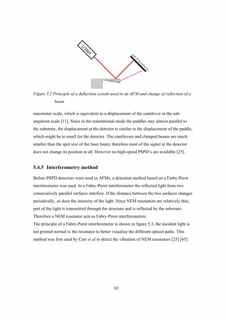
62
Figure 5.2 Principle of a deflection system used in an AFM and change of reflection of a
beam
nanometer scale, which is equivalent to a displacement of the cantilever in the sub-
angstrom scale [11]. Since in the translational mode the paddles stay almost parallel to
the substrate, the displacement at the detector is similar to the displacement of the paddle,
which might be to small for the detector. The cantilevers and clamped beams are much
smaller than the spot size of the laser beam; therefore most of the signal at the detector
does not change its position at all. However no high-speed PSPD’s are available [25].
5.4.5 Interferometry method
Before PSPD detectors were used in AFMs, a detection method based on a Farby-Perot
interferometer was used. In a Fabry-Perot interferometer the reflected light from two
consecutively parallel surfaces interfere. If the distance between the two surfaces changes
periodically, so does the intensity of the light. Since NEM resonators are relatively thin,
part of the light is transmitted through the structure and is reflected by the substrate.
Therefore a NEM resonator acts as Fabry-Perot interferometers.
The principle of a Fabry-Perot interferometer is shown in figure 5.3, the incident light is
not printed normal to the resonator to better visualize the different optical paths. This
method was first used by Carr et al to detect the vibration of NEM resonators [25] [65].
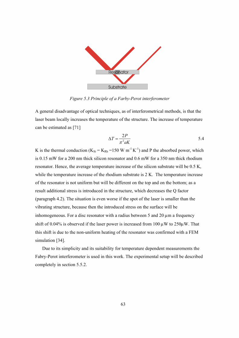
63
Figure 5.3 Principle of a Farby-Perot interferometer
A general disadvantage of optical techniques, as of interferometrical methods, is that the
laser beam locally increases the temperature of the structure. The increase of temperature
can be estimated as [71]
2
2PTaKπ
∆ = 5.4
K is the thermal conduction (KSi = KRh =150 W m-1 K-1) and P the absorbed power, which
is 0.15 mW for a 200 nm thick silicon resonator and 0.6 mW for a 350 nm thick rhodium
resonator. Hence, the average temperature increase of the silicon substrate will be 0.5 K,
while the temperature increase of the rhodium substrate is 2 K. The temperature increase
of the resonator is not uniform but will be different on the top and on the bottom; as a
result additional stress is introduced in the structure, which decreases the Q factor
(paragraph 4.2). The situation is even worse if the spot of the laser is smaller than the
vibrating structure, because then the introduced stress on the surface will be
inhomogeneous. For a disc resonator with a radius between 5 and 20 µm a frequency
shift of 0.04% is observed if the laser power is increased from 100 µW to 250µW. That
this shift is due to the non-uniform heating of the resonator was confirmed with a FEM
simulation [34].
Due to its simplicity and its suitability for temperature dependent measurements the
Fabry-Perot interferometer is used in this work. The experimental setup will be described
completely in section 5.5.2.
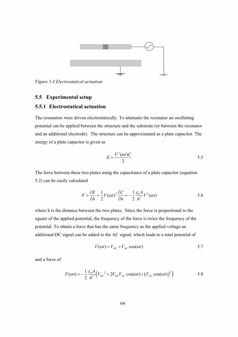
64
Figure 5.4 Electrostatical actuation
5.5 Experimental setup
5.5.1 Electrostatical actuation
The resonators were driven electrostatically. To attenuate the resonator an oscillating
potential can be applied between the structure and the substrate (or between the resonator
and an additional electrode). The structure can be approximated as a plate capacitor. The
energy of a plate capacitor is given as
2 ( )
2V t CE ω
= 5.5
The force between these two plates using the capacitance of a plate capacitor (equation
5.2) can be easily calculated
2 202
1 1( ) ( )2 2
AE CF V t V th h h
εω ω∂ ∂= = = −
∂ ∂ 5.6
where h is the distance between the two plates. Since the force is proportional to the
square of the applied potential, the frequency of the force is twice the frequency of the
potential. To obtain a force that has the same frequency as the applied voltage an
additional DC signal can be added to the AC signal, which leads to a total potential of
( ) cos( )DC ACV t V V tω ω= + 5.7
and a force of
( )( )2202
1( ) 2 cos( ) cos( )2 DC DC AC AC
AF t V V V t V thεω ω ω= − + + 5.8
65
If VAC << VDC the term V2AC cos2(ωt) can be neglected and the force will oscillate with
the same frequency as the potential around a force F0. The DC potential not only creates a
force offset but also increases the amplitude of the oscillation. Due to electrical losses the
potential at the resonator is much smaller than the output potential of the power supply.
Therefore a loss factor α will be introduced in equation 5.8. To simplify the discussion all
prefactors were combined in one factor (Funit)
( ) ( )2 202
1( ) 2 cos( ) 2 cos( )2 DC AC DC unit DC AC DC
AF t V V V t F A V V V thεω α ω ω= − + = + 5.9
5.5.2 Room temperature setup
Since the Fabry-Perot interferometer technique is successfully used to characterize NEM
resonators [34] [65] and is relatively simple to build, the setup for this work is based on
this technique. The laser was a 35 mW helium-neon laser (633nm) from JDS Uniphase,
directly followed by a double concave lens with a focal length of –25 mm to widen the
beam to uniformly illuminate the microscope objective. Approximately 16” away from
the laser a 1” beam splitter cube was set up followed by a Olympus SLMPlan 20x
microscope objective at 13” further. The objective had a numerical aperture of 0.35 and a
working distance of approximately 2 cm. The sample was mounted in a CF 2 ¾” vacuum
tee on an IC socket that was glued on a Teflon spacer. Four of the pins of the IC socket
were connected to the 4 BNC feed-through at the back of the chamber. The ground was
taken from the chamber walls. The tee was closed with a quartz window in the front and
a valve at the side. The chamber was pumped down with a rotary pump below 10 mtorr
before disconnecting the pump for the measurement. This was done to limit the vibration
of the chamber during the measurements, but also to prevent the chamber from tilting
since it was not screwed to the base plate but rested on a U shaped holder. We did not
have the ability to monitor the pressure in the chamber itself. An xyz stage with a
positioning sensitivity of about one micrometer was used to position the chamber.
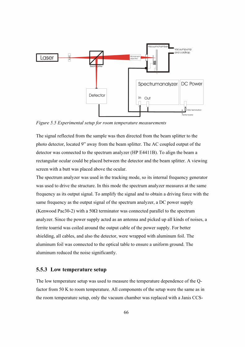
66
Figure 5.5 Experimental setup for room temperature measurements
The signal reflected from the sample was then directed from the beam splitter to the
photo detector, located 9” away from the beam splitter. The AC coupled output of the
detector was connected to the spectrum analyzer (HP E4411B). To align the beam a
rectangular ocular could be placed between the detector and the beam splitter. A viewing
screen with a butt was placed above the ocular.
The spectrum analyzer was used in the tracking mode, so its internal frequency generator
was used to drive the structure. In this mode the spectrum analyzer measures at the same
frequency as its output signal. To amplify the signal and to obtain a driving force with the
same frequency as the output signal of the spectrum analyzer, a DC power supply
(Kenwood Pac30-2) with a 50Ω terminator was connected parallel to the spectrum
analyzer. Since the power supply acted as an antenna and picked up all kinds of noises, a
ferrite toarrid was coiled around the output cable of the power supply. For better
shielding, all cables, and also the detector, were wrapped with aluminum foil. The
aluminum foil was connected to the optical table to ensure a uniform ground. The
aluminum reduced the noise significantly.
5.5.3 Low temperature setup
The low temperature setup was used to measure the temperature dependence of the Q-
factor from 50 K to room temperature. All components of the setup were the same as in
the room temperature setup, only the vacuum chamber was replaced with a Janis CCS-
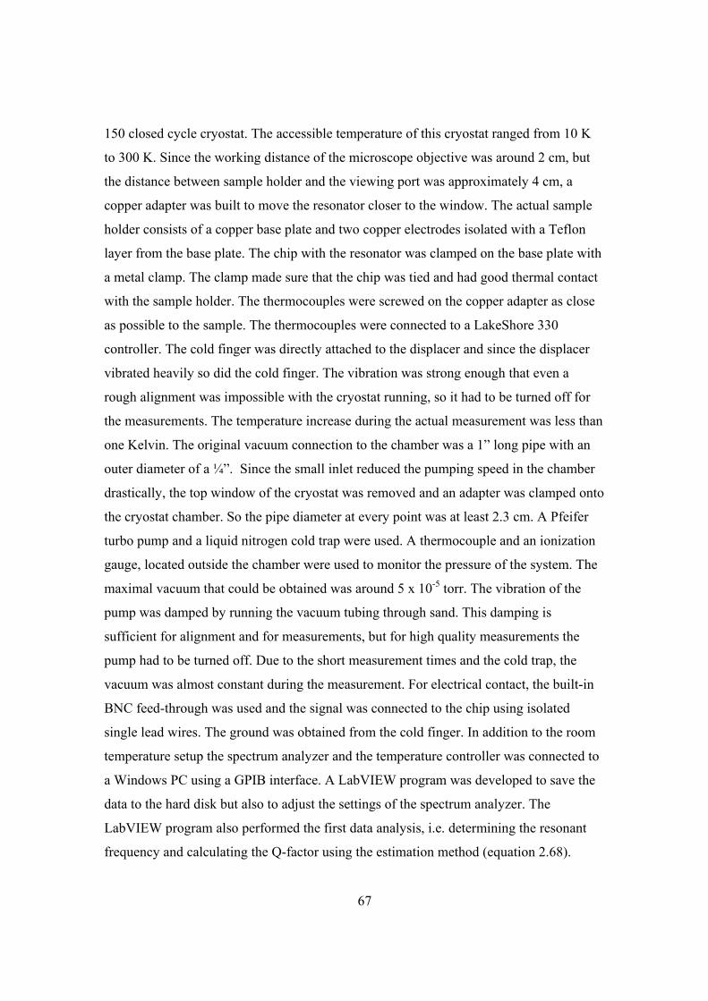
67
150 closed cycle cryostat. The accessible temperature of this cryostat ranged from 10 K
to 300 K. Since the working distance of the microscope objective was around 2 cm, but
the distance between sample holder and the viewing port was approximately 4 cm, a
copper adapter was built to move the resonator closer to the window. The actual sample
holder consists of a copper base plate and two copper electrodes isolated with a Teflon
layer from the base plate. The chip with the resonator was clamped on the base plate with
a metal clamp. The clamp made sure that the chip was tied and had good thermal contact
with the sample holder. The thermocouples were screwed on the copper adapter as close
as possible to the sample. The thermocouples were connected to a LakeShore 330
controller. The cold finger was directly attached to the displacer and since the displacer
vibrated heavily so did the cold finger. The vibration was strong enough that even a
rough alignment was impossible with the cryostat running, so it had to be turned off for
the measurements. The temperature increase during the actual measurement was less than
one Kelvin. The original vacuum connection to the chamber was a 1” long pipe with an
outer diameter of a ¼”. Since the small inlet reduced the pumping speed in the chamber
drastically, the top window of the cryostat was removed and an adapter was clamped onto
the cryostat chamber. So the pipe diameter at every point was at least 2.3 cm. A Pfeifer
turbo pump and a liquid nitrogen cold trap were used. A thermocouple and an ionization
gauge, located outside the chamber were used to monitor the pressure of the system. The
maximal vacuum that could be obtained was around 5 x 10⁻⁵ torr. The vibration of the
pump was damped by running the vacuum tubing through sand. This damping is
sufficient for alignment and for measurements, but for high quality measurements the
pump had to be turned off. Due to the short measurement times and the cold trap, the
vacuum was almost constant during the measurement. For electrical contact, the built-in
BNC feed-through was used and the signal was connected to the chip using isolated
single lead wires. The ground was obtained from the cold finger. In addition to the room
temperature setup the spectrum analyzer and the temperature controller was connected to
a Windows PC using a GPIB interface. A LabVIEW program was developed to save the
data to the hard disk but also to adjust the settings of the spectrum analyzer. The
LabVIEW program also performed the first data analysis, i.e. determining the resonant
frequency and calculating the Q-factor using the estimation method (equation 2.68).
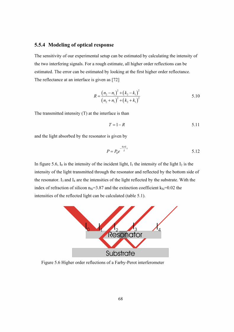
68
5.5.4 Modeling of optical response
The sensitivity of our experimental setup can be estimated by calculating the intensity of
the two interfering signals. For a rough estimate, all higher order reflections can be
estimated. The error can be estimated by looking at the first higher order reflectance.
The reflectance at an interface is given as [72]
( ) ( )( ) ( )
2 22 1 2 1
2 22 1 2 1
n n k kR
n n k k− + −
=+ + +
5.10
The transmitted intensity (T) at the interface is than
1T R= − 5.11
and the light absorbed by the resonator is given by
4
0
k tP P e
πλ
−= 5.12
In figure 5.6, I0 is the intensity of the incident light, I1 the intensity of the light I2 is the
intensity of the light transmitted through the resonator and reflected by the bottom side of
the resonator. I3 and I4 are the intensities of the light reflected by the substrate. With the
index of refraction of silicon nSi=3.87 and the extinction coefficient kSi=0.02 the
intensities of the reflected light can be calculated (table 5.1).
Resonator
Substrate
I0 I4I3I1 I2
Figure 5.6 Higher order reflections of a Farby-Perot interferometer
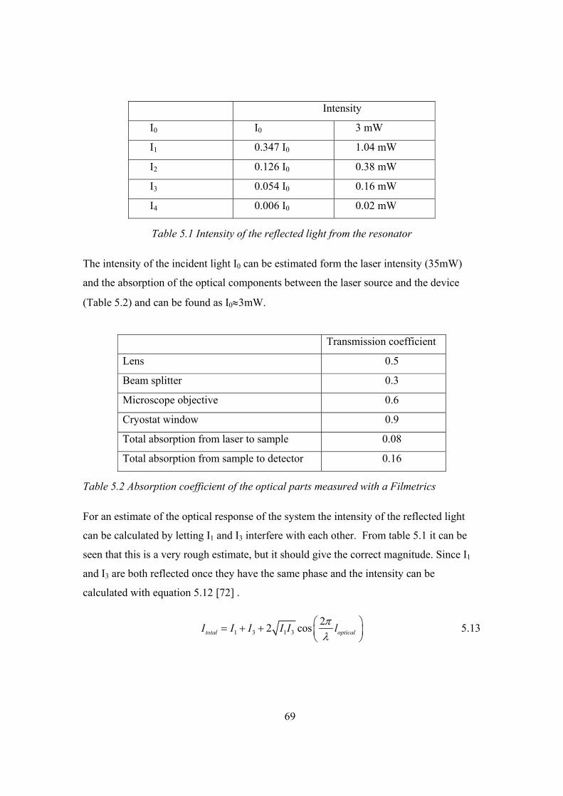
69
Intensity
I0 I0 3 mW
I1 0.347 I0 1.04 mW
I2 0.126 I0 0.38 mW
I3 0.054 I0 0.16 mW
I4 0.006 I0 0.02 mW
Table 5.1 Intensity of the reflected light from the resonator
The intensity of the incident light I0 can be estimated form the laser intensity (35mW)
and the absorption of the optical components between the laser source and the device
(Table 5.2) and can be found as I0≈3mW.
Transmission coefficient
Lens 0.5
Beam splitter 0.3
Microscope objective 0.6
Cryostat window 0.9
Total absorption from laser to sample 0.08
Total absorption from sample to detector 0.16
Table 5.2 Absorption coefficient of the optical parts measured with a Filmetrics
For an estimate of the optical response of the system the intensity of the reflected light
can be calculated by letting I1 and I3 interfere with each other. From table 5.1 it can be
seen that this is a very rough estimate, but it should give the correct magnitude. Since I1
and I3 are both reflected once they have the same phase and the intensity can be
calculated with equation 5.12 [72] .
1 3 1 322 costotal opticalI I I I I lπλ
= + +
5.13
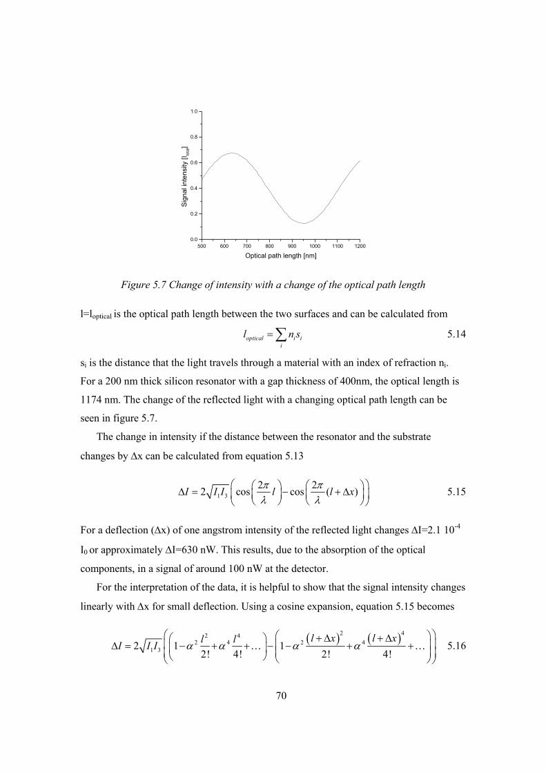
70
500 600 700 800 900 1000 1100 12000.0
0.2
0.4
0.6
0.8
1.0
Optical path length [nm]
Sign
al in
tens
ity [I
tota
l]
Figure 5.7 Change of intensity with a change of the optical path length
l=loptical is the optical path length between the two surfaces and can be calculated from
optical i ii
l n s= ∑ 5.14
si is the distance that the light travels through a material with an index of refraction ni.
For a 200 nm thick silicon resonator with a gap thickness of 400nm, the optical length is
1174 nm. The change of the reflected light with a changing optical path length can be
seen in figure 5.7.
The change in intensity if the distance between the resonator and the substrate
changes by ∆x can be calculated from equation 5.13
1 32 22 cos cos ( )I I I l l xπ πλ λ
∆ = − + ∆
5.15
For a deflection (∆x) of one angstrom intensity of the reflected light changes ∆I=2.1 10-4
I0 or approximately ∆I=630 nW. This results, due to the absorption of the optical
components, in a signal of around 100 nW at the detector.
For the interpretation of the data, it is helpful to show that the signal intensity changes
linearly with ∆x for small deflection. Using a cosine expansion, equation 5.15 becomes
( ) ( )2 42 42 4 2 4
1 32 1 12! 4! 2! 4!
l x l xl lI I I α α α α + ∆ + ∆ ∆ = − + + − − + +
K K 5.16
71
where α=2πλ-1. Since ∆x << l all higher order terms of ∆x can be neglected, equation
5.16 becomes
2 4 2 42 4 2 4
1 3 32 4
1 12! 4! 2! 4!
22 42! 4!
l l l l
I I Il lx
α α α α
α α
− + + − − + +
∆ = +∆ − +
K K
K
5.17
or simply
2 3
2 41 3 2
2 482! 4!l lI I I xπ α α
λ
∆ = ∆ − +
K 5.18
5.5.5 Sensitivity of the Detector
The detector used for this work was a 1 GHz low noise detector from New Focus (model
1601). The detector has a noise-equivalent power (NEP) of 38 pW/Hz-1/2 and a gain of
300 V/W at 633 nm. The bandwidth (BW) of the spectrum analyzer was 5 kHz. The
minimum detectable signal can be calculated as a product of NEP and BW1/2 and is
therefore 2.6 nW, which would yield in an electrical signal of 0.8 µV. Since the noise
level of the electrical equipment is in the same magnitude, intensity changes of the signal
larger than 3 nW can be detected. A deflection of 1 Å results in an intensity change of ∆I
=100 nW at the detector or a signal of 30 µV. The setup is therefore sufficient to detect
sub-nanometer scale motion, even if structure is much smaller than the diameter of the
incident laser beam.
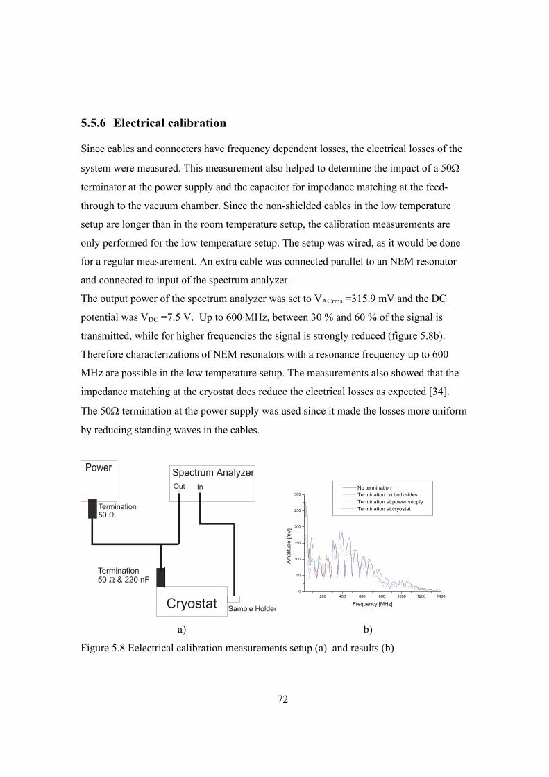
72
5.5.6 Electrical calibration
Since cables and connecters have frequency dependent losses, the electrical losses of the
system were measured. This measurement also helped to determine the impact of a 50Ω
terminator at the power supply and the capacitor for impedance matching at the feed-
through to the vacuum chamber. Since the non-shielded cables in the low temperature
setup are longer than in the room temperature setup, the calibration measurements are
only performed for the low temperature setup. The setup was wired, as it would be done
for a regular measurement. An extra cable was connected parallel to an NEM resonator
and connected to input of the spectrum analyzer.
The output power of the spectrum analyzer was set to VACrms =315.9 mV and the DC
potential was VDC =7.5 V. Up to 600 MHz, between 30 % and 60 % of the signal is
transmitted, while for higher frequencies the signal is strongly reduced (figure 5.8b).
Therefore characterizations of NEM resonators with a resonance frequency up to 600
MHz are possible in the low temperature setup. The measurements also showed that the
impedance matching at the cryostat does reduce the electrical losses as expected [34].
The 50Ω termination at the power supply was used since it made the losses more uniform
by reducing standing waves in the cables.
200 400 600 800 1000 1200 14000
50
100
150
200
250
300 No termination Termination on both sides Termination at power supply Termination at cryostat
Ampl
itude
[mV]
Frequency [MHz]
a) b)
Figure 5.8 Eelectrical calibration measurements setup (a) and results (b)
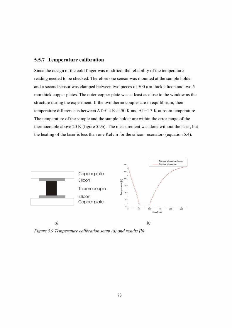
73
5.5.7 Temperature calibration
Since the design of the cold finger was modified, the reliability of the temperature
reading needed to be checked. Therefore one sensor was mounted at the sample holder
and a second sensor was clamped between two pieces of 500 µm thick silicon and two 5
mm thick copper plates. The outer copper plate was at least as close to the window as the
structure during the experiment. If the two thermocouples are in equilibrium, their
temperature difference is between ∆T=0.4 K at 50 K and ∆T=1.3 K at room temperature.
The temperature of the sample and the sample holder are within the error range of the
thermocouple above 20 K (figure 5.9b). The measurement was done without the laser, but
the heating of the laser is less than one Kelvin for the silicon resonators (equation 5.4).
0 50 100 150 200 2500
50
100
150
200
250
300
Sensor at sample holder Sensor at sample
Tem
pera
ture
[K]
time [min]
a) b)
Figure 5.9 Temperature calibration setup (a) and results (b)
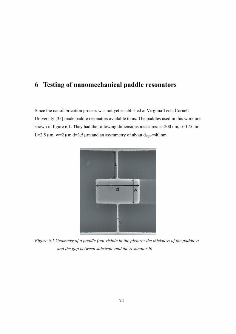
74
6 Testing of nanomechanical paddle resonators
Since the nanofabrication process was not yet established at Virginia Tech, Cornell
University [35] made paddle resonators available to us. The paddles used in this work are
shown in figure 6.1. They had the following dimensions measures: a=200 nm, b=175 nm,
L=2.5 µm, w=2 µm d=3.5 µm and an asymmetry of about dasym=40 nm.
d w
L
b
Figure 6.1 Geometry of a paddle (not visible in the picture: the thickness of the paddle a
and the gap between substrate and the resonator h)
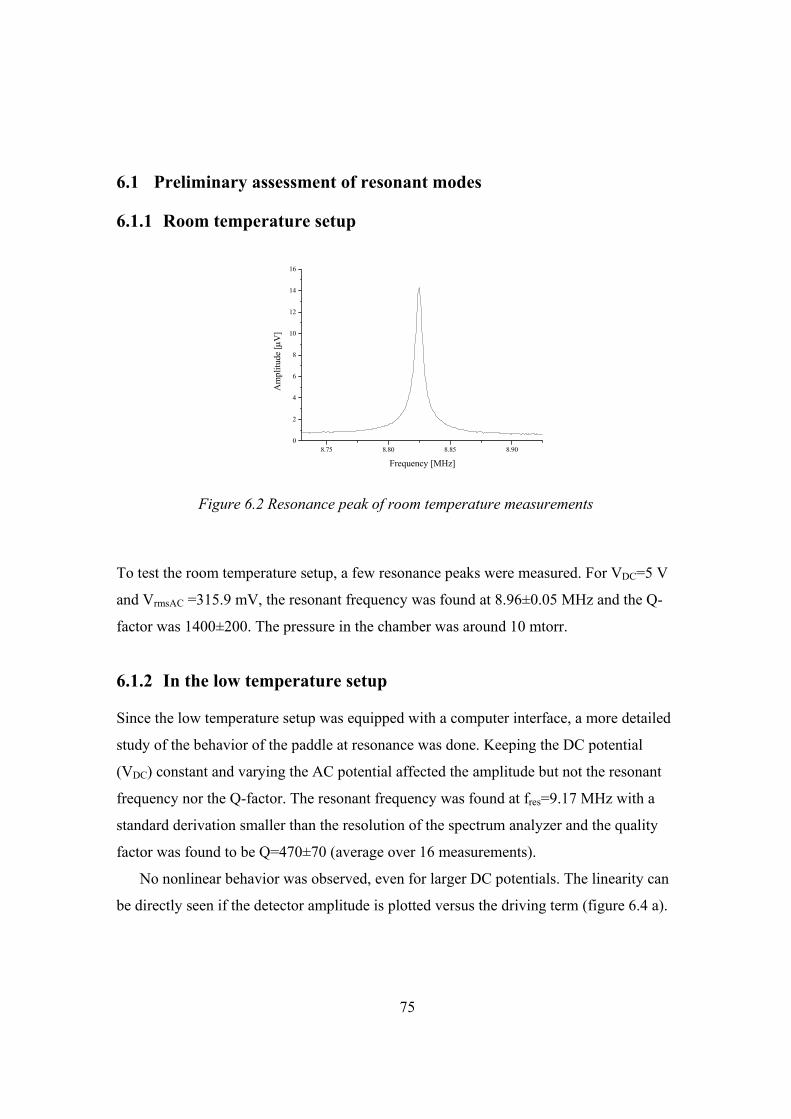
75
6.1 Preliminary assessment of resonant modes
6.1.1 Room temperature setup
8.75 8.80 8.85 8.900
2
4
6
8
10
12
14
16A
mpl
itude
[µV
]
Frequency [MHz]
Figure 6.2 Resonance peak of room temperature measurements
To test the room temperature setup, a few resonance peaks were measured. For VDC=5 V
and VrmsAC =315.9 mV, the resonant frequency was found at 8.96±0.05 MHz and the Q-
factor was 1400±200. The pressure in the chamber was around 10 mtorr.
6.1.2 In the low temperature setup
Since the low temperature setup was equipped with a computer interface, a more detailed
study of the behavior of the paddle at resonance was done. Keeping the DC potential
(VDC) constant and varying the AC potential affected the amplitude but not the resonant
frequency nor the Q-factor. The resonant frequency was found at fres=9.17 MHz with a
standard derivation smaller than the resolution of the spectrum analyzer and the quality
factor was found to be Q=470±70 (average over 16 measurements).
No nonlinear behavior was observed, even for larger DC potentials. The linearity can
be directly seen if the detector amplitude is plotted versus the driving term (figure 6.4 a).
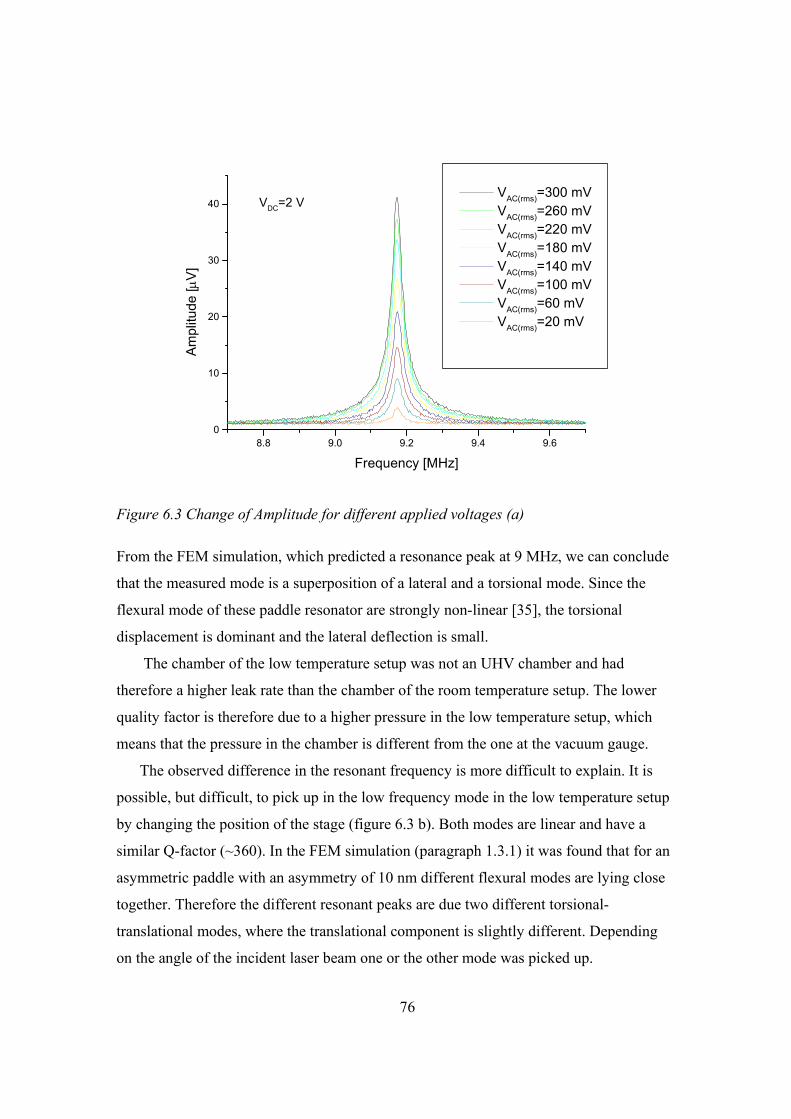
76
8.8 9.0 9.2 9.4 9.60
10
20
30
40 VDC=2 V VAC(rms)=300 mV VAC(rms)=260 mV VAC(rms)=220 mV VAC(rms)=180 mV VAC(rms)=140 mV VAC(rms)=100 mV VAC(rms)=60 mV VAC(rms)=20 mV
Ampl
itude
[µV]
Frequency [MHz]
Figure 6.3 Change of Amplitude for different applied voltages (a)
From the FEM simulation, which predicted a resonance peak at 9 MHz, we can conclude
that the measured mode is a superposition of a lateral and a torsional mode. Since the
flexural mode of these paddle resonator are strongly non-linear [35], the torsional
displacement is dominant and the lateral deflection is small.
The chamber of the low temperature setup was not an UHV chamber and had
therefore a higher leak rate than the chamber of the room temperature setup. The lower
quality factor is therefore due to a higher pressure in the low temperature setup, which
means that the pressure in the chamber is different from the one at the vacuum gauge.
The observed difference in the resonant frequency is more difficult to explain. It is
possible, but difficult, to pick up in the low frequency mode in the low temperature setup
by changing the position of the stage (figure 6.3 b). Both modes are linear and have a
similar Q-factor (~360). In the FEM simulation (paragraph 1.3.1) it was found that for an
asymmetric paddle with an asymmetry of 10 nm different flexural modes are lying close
together. Therefore the different resonant peaks are due two different torsional-
translational modes, where the translational component is slightly different. Depending
on the angle of the incident laser beam one or the other mode was picked up.
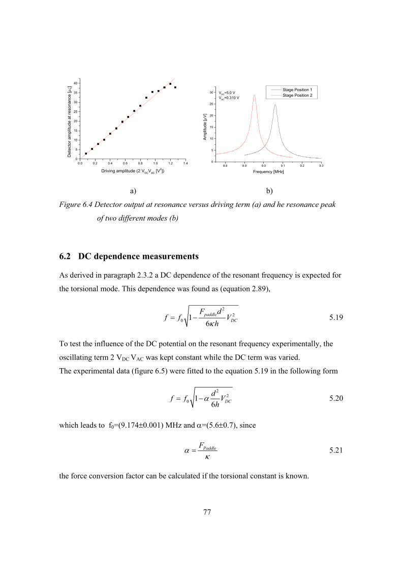
77
0.0 0.2 0.4 0.6 0.8 1.0 1.2 1.40
5
10
15
20
25
30
35
40
Det
ecto
r am
plitu
de a
t res
onan
ce [µ
ς]
Driving amplitude (2 VDCVAC [V2])8.8 8.9 9.0 9.1 9.2 9.3
0
5
10
15
20
25
30 VDC=5.0 VVAC=0.310 V
Stage Position 1 Stage Position 2
Ampl
itude
[µV]
Frequency [MHz]
a) b)
Figure 6.4 Detector output at resonance versus driving term (a) and he resonance peak
of two different modes (b)
6.2 DC dependence measurements
As derived in paragraph 2.3.2 a DC dependence of the resonant frequency is expected for
the torsional mode. This dependence was found as (equation 2.89),
2
20 1
6paddle
DC
F df f V
hκ= − 5.19
To test the influence of the DC potential on the resonant frequency experimentally, the
oscillating term 2 VDC VAC was kept constant while the DC term was varied.
The experimental data (figure 6.5) were fitted to the equation 5.19 in the following form
2
20 1
6 DCdf f V
hα= − 5.20
which leads to f0=(9.174±0.001) MHz and α=(5.6±0.7), since
PaddleFακ
= 5.21
the force conversion factor can be calculated if the torsional constant is known.
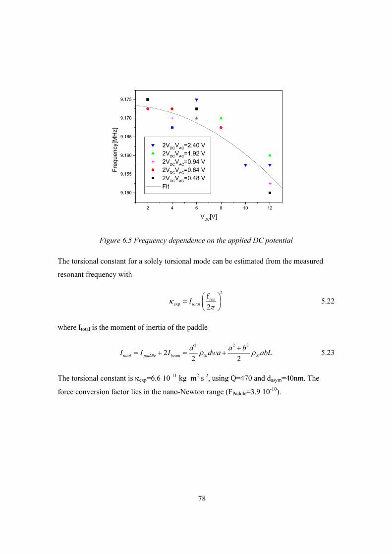
78
2 4 6 8 10 12
9.150
9.155
9.160
9.165
9.170
9.175
2VDCVAC=2.40 V 2VDCVAC=1.92 V 2VDCVAC=0.94 V 2VDCVAC=0.64 V 2VDCVAC=0.48 V Fit
Freq
uenc
y[M
Hz]
VDC[V]
Figure 6.5 Frequency dependence on the applied DC potential
The torsional constant for a solely torsional mode can be estimated from the measured
resonant frequency with
2
expf2
restotalIκ
π =
5.22
where Itotal is the moment of inertia of the paddle
2 2 2
22 2total paddle beam Si Si
d a bI I I dwa abLρ ρ+= + = + 5.23
The torsional constant is κexp=6.6 10-11 kg m2 s-2, using Q=470 and dasym=40nm. The
force conversion factor lies in the nano-Newton range (FPaddle=3.9 10-10).
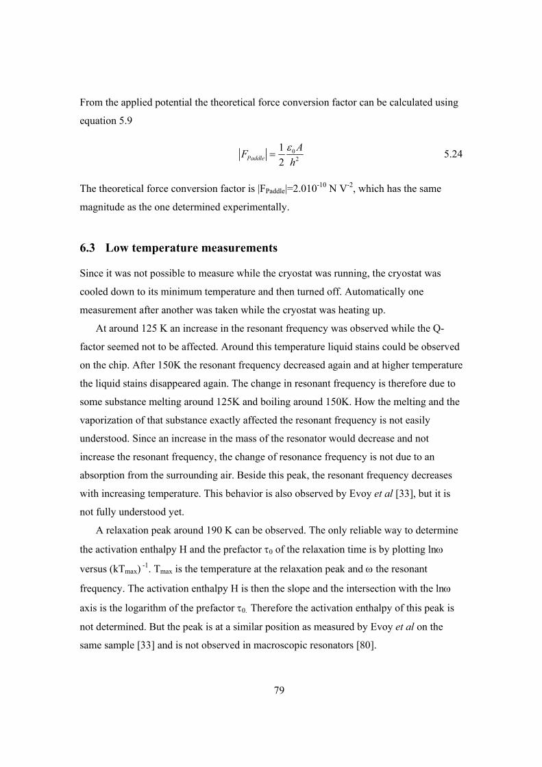
79
From the applied potential the theoretical force conversion factor can be calculated using
equation 5.9
02
12Paddle
AFhε
= 5.24
The theoretical force conversion factor is |FPaddle|=2.010-10 N V-2, which has the same
magnitude as the one determined experimentally.
6.3 Low temperature measurements
Since it was not possible to measure while the cryostat was running, the cryostat was
cooled down to its minimum temperature and then turned off. Automatically one
measurement after another was taken while the cryostat was heating up.
At around 125 K an increase in the resonant frequency was observed while the Q-
factor seemed not to be affected. Around this temperature liquid stains could be observed
on the chip. After 150K the resonant frequency decreased again and at higher temperature
the liquid stains disappeared again. The change in resonant frequency is therefore due to
some substance melting around 125K and boiling around 150K. How the melting and the
vaporization of that substance exactly affected the resonant frequency is not easily
understood. Since an increase in the mass of the resonator would decrease and not
increase the resonant frequency, the change of resonance frequency is not due to an
absorption from the surrounding air. Beside this peak, the resonant frequency decreases
with increasing temperature. This behavior is also observed by Evoy et al [33], but it is
not fully understood yet.
A relaxation peak around 190 K can be observed. The only reliable way to determine
the activation enthalpy H and the prefactor τ0 of the relaxation time is by plotting lnω
versus (kTmax) -1. Tmax is the temperature at the relaxation peak and ω the resonant
frequency. The activation enthalpy H is then the slope and the intersection with the lnω
axis is the logarithm of the prefactor τ0. Therefore the activation enthalpy of this peak is
not determined. But the peak is at a similar position as measured by Evoy et al on the
same sample [33] and is not observed in macroscopic resonators [80].
80
50 100 150 200 2500
5
10
Freq
uenc
y [M
Hz]
1/Q
[10-3
]
T [K]
8.9
9.0
9.1
9.2
9.3
9.4
9.5
Figure 6.6 Temperature dependence of Q-factor and frequency
It is interesting to note, that for temperature below 150 K it was much easier to get
reliable and reproducible measurements. The paddle reaches the same quality factor as
for the room temperature setup at very low temperature (~60K). This indicates that the
pressure at these low temperatures is similar to the room temperature setup. Which means
that the cold finger of the cryostat acts as cryogenic pump at low temperatures. This also
explains why the height of the relaxation peak measured in this experiment is much
higher than the one measured by Evoy et al [30].
6.4 Conclusion
Sub nanometer vibration of a torsional-translational mode was measured with this setup.
The measured resonant frequency agrees with the one predicted by the FEM simulation.
Since no translational mode was dedected it might be possible that the setup did not pick
up the vibration as a Fabry-Perot interferometer, but simple that the tilted paddle reflected
part of the light away from the detector. Forces in the nano Newton regime can be
detected with a torsional paddle resonator. However a better vacuum is needed to make
reliable temperature dependent measurement. This and other possible improvements of
the setup are discussed in chapter eight.
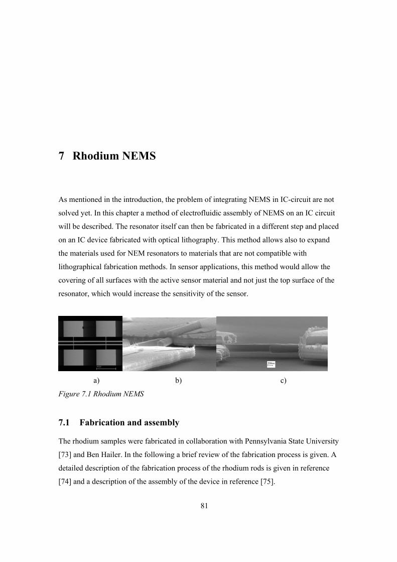
81
7 Rhodium NEMS
As mentioned in the introduction, the problem of integrating NEMS in IC-circuit are not
solved yet. In this chapter a method of electrofluidic assembly of NEMS on an IC circuit
will be described. The resonator itself can then be fabricated in a different step and placed
on an IC device fabricated with optical lithography. This method allows also to expand
the materials used for NEM resonators to materials that are not compatible with
lithographical fabrication methods. In sensor applications, this method would allow the
covering of all surfaces with the active sensor material and not just the top surface of the
resonator, which would increase the sensitivity of the sensor.
a) b) c)
Figure 7.1 Rhodium NEMS
7.1 Fabrication and assembly
The rhodium samples were fabricated in collaboration with Pennsylvania State University
[73] and Ben Hailer. In the following a brief review of the fabrication process is given. A
detailed description of the fabrication process of the rhodium rods is given in reference
[74] and a description of the assembly of the device in reference [75].
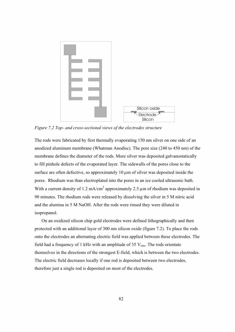
82
Figure 7.2 Top- and cross-sectional views of the electrodes structure
The rods were fabricated by first thermally evaporating 150 nm silver on one side of an
anodized aluminum membrane (Whatman Anodisc). The pore size (240 to 450 nm) of the
membrane defines the diameter of the rods. More silver was deposited galvanostatically
to fill pinhole defects of the evaporated layer. The sidewalls of the pores close to the
surface are often defective, so approximately 10 µm of silver was deposited inside the
pores. Rhodium was than electroplated into the pores in an ice cooled ultrasonic bath.
With a current density of 1.2 mA/cm2 approximately 2.5 µm of rhodium was deposited in
90 minutes. The rhodium rods were released by dissolving the silver in 5 M nitric acid
and the alumina in 5 M NaOH. After the rods were rinsed they were diluted in
isopropanol.
On an oxidized silicon chip gold electrodes were defined lithographically and then
protected with an additional layer of 300 nm silicon oxide (figure 7.2). To place the rods
onto the electrodes an alternating electric field was applied between these electrodes. The
field had a frequency of 1 kHz with an amplitude of 35 Vrms. The rods orientate
themselves in the directions of the strongest E-field, which is between the two electrodes.
The electric field decreases locally if one rod is deposited between two electrodes,
therefore just a single rod is deposited on most of the electrodes.
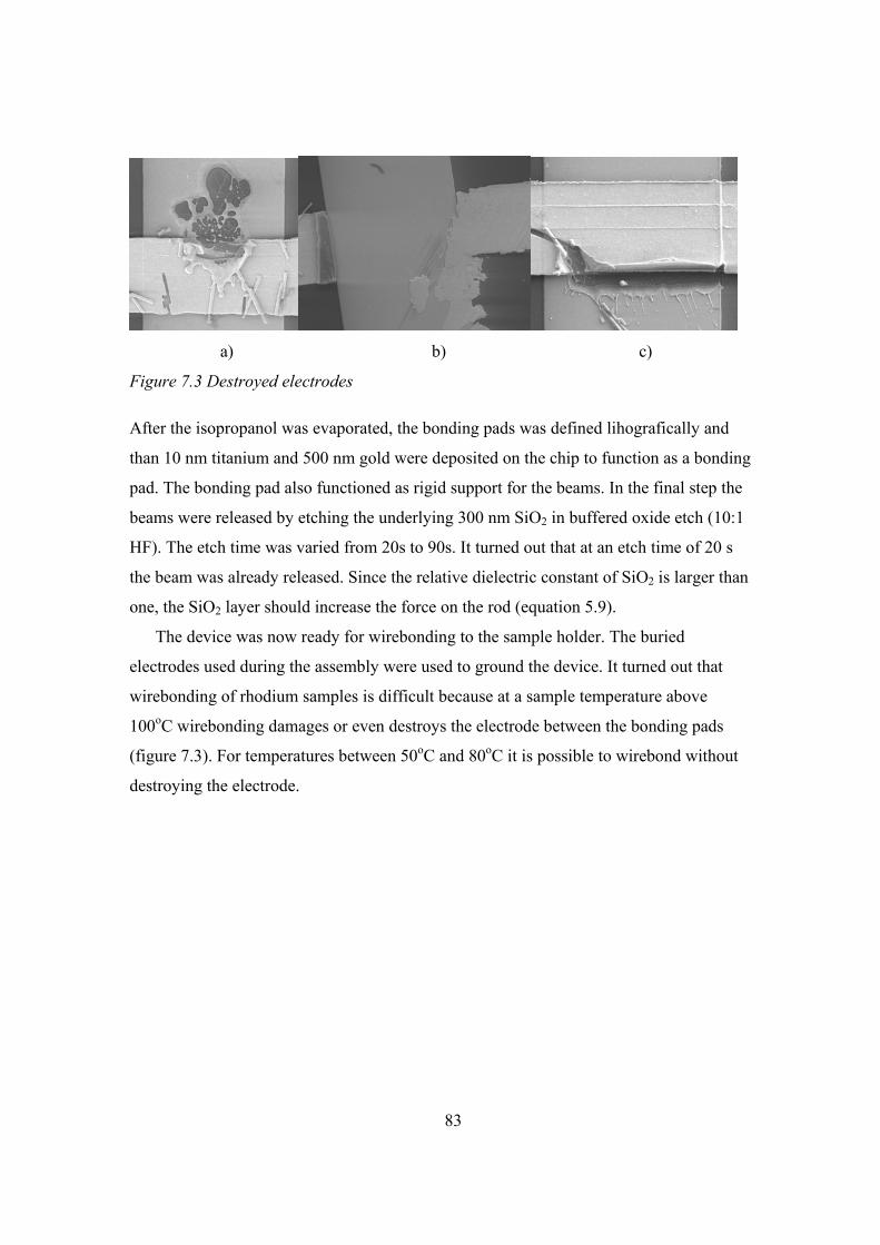
83
a) b) c)
Figure 7.3 Destroyed electrodes
After the isopropanol was evaporated, the bonding pads was defined lihografically and
than 10 nm titanium and 500 nm gold were deposited on the chip to function as a bonding
pad. The bonding pad also functioned as rigid support for the beams. In the final step the
beams were released by etching the underlying 300 nm SiO2 in buffered oxide etch (10:1
HF). The etch time was varied from 20s to 90s. It turned out that at an etch time of 20 s
the beam was already released. Since the relative dielectric constant of SiO2 is larger than
one, the SiO2 layer should increase the force on the rod (equation 5.9).
The device was now ready for wirebonding to the sample holder. The buried
electrodes used during the assembly were used to ground the device. It turned out that
wirebonding of rhodium samples is difficult because at a sample temperature above
100oC wirebonding damages or even destroys the electrode between the bonding pads
(figure 7.3). For temperatures between 50oC and 80oC it is possible to wirebond without
destroying the electrode.
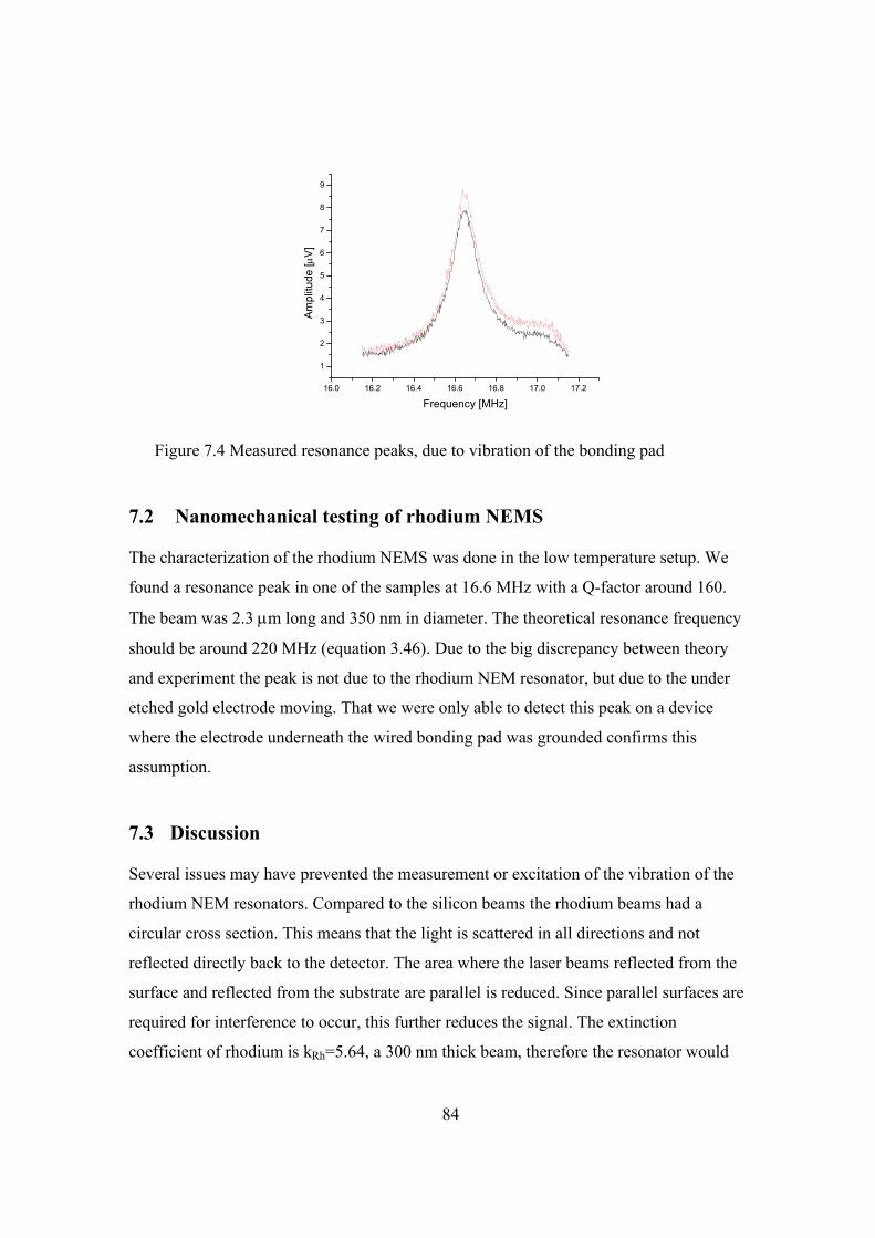
84
16.0 16.2 16.4 16.6 16.8 17.0 17.2
1
2
3
4
5
6
7
8
9
Ampl
itude
[µV]
Frequency [MHz]
Figure 7.4 Measured resonance peaks, due to vibration of the bonding pad
7.2 Nanomechanical testing of rhodium NEMS
The characterization of the rhodium NEMS was done in the low temperature setup. We
found a resonance peak in one of the samples at 16.6 MHz with a Q-factor around 160.
The beam was 2.3 µm long and 350 nm in diameter. The theoretical resonance frequency
should be around 220 MHz (equation 3.46). Due to the big discrepancy between theory
and experiment the peak is not due to the rhodium NEM resonator, but due to the under
etched gold electrode moving. That we were only able to detect this peak on a device
where the electrode underneath the wired bonding pad was grounded confirms this
assumption.
7.3 Discussion
Several issues may have prevented the measurement or excitation of the vibration of the
rhodium NEM resonators. Compared to the silicon beams the rhodium beams had a
circular cross section. This means that the light is scattered in all directions and not
reflected directly back to the detector. The area where the laser beams reflected from the
surface and reflected from the substrate are parallel is reduced. Since parallel surfaces are
required for interference to occur, this further reduces the signal. The extinction
coefficient of rhodium is kRh=5.64, a 300 nm thick beam, therefore the resonator would
85
only transmit 2.6 x 10⁻¹⁵ of the incident light, which makes interference impossible. But
also the bonding pad is opaque, whose vibration we where able to pick up. This again
confirms that our experimental system not only picks vibration with Farby-Perot
interferometry but that the change of the reflectance angle changes the signal enough to
detect vibration.
Since the resistivity of silicon is relatively high it is more likely that the force does
not act between the beam and the substrate underneath, but directly between the electrode
and the beam. Due to the large distance between the electrode and the beam the force is
neglectably small (400 times smaller, compared to an electrode underneath the beam).
For a 3 µm long beam with a diameter of 300 nm keff=50.1, which is a factor of 3.5
smaller than for a silicon double clamped beam, whose resonant frequency is already
measured with a similar setup [76]. But since the rhodium NEM resonators are
polycrystalline structures, the quality factors compared to crystalline silicon resonators is
smaller. Also the clamping losses are expected to be higher since for the silicon NEMS
the support and the beam is one piece, while the rhodium NEMS are clamped between a
layer of SiO2 and a gold layer, which means that microslip can occur, especially at the
support edges, where the SiO2 is etched away. The vibration amplitude is therefore
smaller than for a silicon NEM resonator.
7.4 Outlook
By depositing an additional electrode underneath the beam the problem with the bad
electrical grounding can be overcome. The relative dielectric constant of SiO2 is 3.9. A
remaining SiO2-layer on the electrode would therefore increase the force on the beam
compared to an air gap. Hence just enough SiO2 to release the beam should be removed.
Increasing the thickness of the bonding pad can reduce the clamping losses. Since
rhodium is a relatively good conductor it also would be worth trying the magnetic
detection method to detect the vibration (paragraph 5.4.2).
86
8 Improvements of the Setup
In this chapter recommendations are made for the improvement of the nanomechanical
test setup developed in this work. Such improvements would allow more thorough
research on surface-related loss mechanisms.
8.1 Optical
Alignment of the laser beam was difficult due to the inability to precisely align each part.
A micrometer precise alignment in all three translational directions is recommended.
Larger lenses would reduce the observed edge effects. The absorption coefficient of the
optical parts used in this setup was comparably high, using parts with less absorption
would increase the signal at the detector, which would result in the ability to detect even
smaller vibrations. The size of the smallest device whose vibration can be detected is
limited by diffraction. If the size of the resonators would be further reduced, it might be
necessary to reduce the wavelength. Reducing the wavelength would have another
advantage; the extinction coefficient of rhodium would be reduced to kRh=3.1 for violet
light, which would result in a higher signal (for silicon k would increase to kSi=0.3).
A big improvement in the quality of the setup would be achieved by using optical
fiber to transport the signal to the structure and pick it up again. Such fiber would make
the XYZ stage unnecessary, because the fiber itself could easily be moved to illuminate
the sample. The chamber can than be screwed directly to the optical table which would
reduce the vibration of the chamber. Concerns are raised that detecting a signal with
optical fiber might already fail when the size of the device becomes much smaller than
the diameter of the fiber, which would be long before the diffraction limit [17]. Before
employing this method the theoretical resolution limit has to be calculated.
87
8.2 Electrical
The noise had the same level than the smallest detectable signal, to increase the
sensitivity of the setup the noise should be therefore reduced. This could probably be
accomplished by grounding the whole chamber and all of the equipment. As stated
earlier, the power supply acted as an antenna, so a filter that cuts out all AC signals
between the power supply and the rest of the system might be necessary. The noise could
be further reduced if shielded cables, were also used in the vacuum chamber. A better
conducting substrate would further decrease the electrical losses and could be achieved
by doping the wafer from its backside. Also a metalized bonding pad would decrease the
electrical losses while the resonator itself should be left without metal to obtain a high
quality factor.
8.3 Room temperature setup
While the pressure in the room temperature setup was low enough to eliminate air
friction, a better vacuum is needed to study surface related loss mechanisms. The better
vacuum would reduce absorption and desorption at the surface.
Since it has no moving parts, an ion pump would be the best choice to obtain a higher
vacuum. Not only does it not vibrate but it can also be used as a vacuum gauge. The
higher limit of the working pressure of an ion pump can be obtained with a regular rotary
pump. A diffusion pump that also has no vibrating parts is not a good choice since back
streaming oil can contaminate the sample. To decrease the pump down time an additional
turbo pump can be used. This would also allow starting the ion pump at a lower pressure,
which means that the ion pump could run longer in the non-saturated mode, where the
pumping speed is much higher. If the chamber is baked out overnight a vacuum of 10-8
torr could easily be obtained, but even lower pressures should be possible.
If the system is vented with argon the pump down time can be reduced, because it
terminates the surfaces of the chamber better than nitrogen and therefore reduces the
amount of water that condenses on the surfaces when they are exposed to air.
To make sure that the effective pumping speed at the sample is not drastically
reduced, the Teflon spacer should have large holes, or better yet, be replaced by a metal
88
cross that is soldered to the chamber walls. The vacuum gauge should be mounted
directly in the chamber. The sensitivity to vibration can be reduced if a vacuum cross is
used, where one outlet is directly screwed to the base plate.
An integrated sample heater would be helpful to remove all the water on the sample
and also to look into the behavior at higher temperatures, which could reveal further
relaxation peaks. A sample heater that can reach temperatures up to 200° C can be
implanted relatively easily at low cost (less than $ 200). Higher temperatures would be
possible but would need some more changes to the setup. The ability to reach higher
temperatures (>>8000C) would allow annealing the device in the vacuum chamber and
making measurements without exposing it to air between treatment and measurement. If
the chamber has a flow controlled inlet for processing gasses, it would be possible for
example to terminate the surface with H2 by annealing it in an H2 atmosphere. Also, in
situ measurement during an oxidation process might be possible.
8.4 Low temperature setup
The quality of the temperature dependent measurements can be increased if the
cryostat were to run during the measurement. However the cryostat must not introduce
any vibration into the sample, which requires either a liquid flow cryostat or a mechanical
decoupling between the cold finger and the displacer. Closed cycle cryostats where the
cold finger is mechanically decoupled from the displacer would reduce the vibration of
the sample to 3-5 nm [77]. This displacement should be small enough to allow
measurements while the cryostat is left on. The major advantage of this system is that no
liquid helium is consumed during the operation which reduces the operation costs
drastically. In addition, due to the decoupling of the sample from the chamber,
measurements can be done with a running turbo pump, which makes an ion pump
unnecessary. The advantage of a liquid flow cryostat is that temperatures down to 1.4 K
can be easily achieved if He3 is used, while the temperature of most closed circuit
cryostats is limited to 10 K. For most cryostats a higher temperature option is available
where temperatures up to 800 K can be attained. This would allow the characterization of
a sample at the full temperature range without exposing it to air.
89
It is very crucial to have a high vacuum before the cool down processes starts,
because otherwise the cold finger acts as a cryogenic pump and the pressure would
change with temperature.
8.5 New detection method
For measuring the vibration of higher frequencies with a smaller amplitude than the one
of the paddle resonator, another detection method is needed. A technique based on a
scanning tunneling microscope (STM) can be used to measure the vibration of an NEM
resonator. In an STM, the tip is approximately 10 Å away from the sample and if the
separation between the sample and tip changes, by an angstrom, the tunnel current
changes by an order of magnitude [11], which leads to the high resolution of an STM. If
an STM-tip is placed above a resonator, the tunnel current should change with the
position of the tip. To measure a tunneling current a DC bias has to be applied between
the tip and resonator. This bias has to have the same magnitude as the DC potential used
to excite the structure, so a tunnel current might already be measurable if the tip is
grounded, otherwise it might be necessary to ground the resonator itself and apply the
oscillating potential to excite the resonator to the substrate. Since this method needs no
laser, the sample does not heat up during measurements and the experiment can also be
done in the inner of a vacuum chamber far away from a viewing port, which enables
measurements at even lower temperatures.
90
9 Conclusion and further work
This project had three objectives: The first objective was to setup an electron beam
lithography tool and to develop a nanofabrication process. The second was to review
existing vibration models and to develop an adequate model of the vibration of NEM
resonators. The third objective was to develop a test setup for temperature-dependent
experimental testing of NEM resonators.
In chapter two, after reviewing the fundamentals of vibration, an adequate model for
the translational mode was described. In chapter three and four the loss mechanism of
NEM resonators has been reviewed. Electron beam lithography and the fabrication
process of silicon NEMS have been described in the first quarter of chapter five. The first
nanostructure was fabricated as part of this work (figure 5.1a). Since the emphasis of this
work was to develop a test setup for temperature dependent experimental testing of NEM
resonators the rest of chapter five was dedicated to the setup. Different detection methods
have been compared and then the actual setup has been described. The successful
detection of sub-nanometer vibration and the dependency of the quality factor on
temperature has been reported in chapter six. In chapter seven a new fabrication approach
for NEM resonators using electrofluidic assembly was introduced and the first
characterization attempts have been discussed. In chapter eight improvements of the
existing setup have been suggested.
91
9.1 Further work
Since an additional relaxation peak can be observed in NEM resonators compared to
macroscopic resonators, it is most likely that this peak is due to surface related losses, but
its more specific origin has not yet been determined.
Other materials that have a more stable surface, might be used to obtain higher Q-
factors, but these materials have the big disadvantage that they cannot easily be integrated
to standard IC-fabrication processes. Therefore, besides the aspect of surface science,
from a technology point of view it is beneficial to work on the understanding of loss
mechanisms of silicon NEMS, because only with an understanding of underlying loss
mechanism it is possible to design high quality NEM resonators.
For the experimental studies, cantilever resonators seem to be the best choice. Paddle
resonators have the advantage that they produce a larger signal due to their larger size,
but for simpler structures, like a double clamped beam or a cantilever, it is much easier to
model their resonance behavior or their loss mechanisms. This allows a better
comparison between experiment and theory. Cantilevers are preferable over double
clamped beams due to their larger resonance amplitude, which makes it easier to pick up
their vibration. It is further preferable to space the cantilever so that just one cantilever is
measured at a time. With harp structures [73], for example, it is not possible to
differentiate between the higher mode of a shorter beam and the fundamental mode of a
larger beam. To obtain a comprehensive understanding of the relevant loss mechanism,
the temperature should be varied not only from 50 K to room temperature, but from at
least 1.4 K [59] to almost the melting point of the material. Further the experiments must
be done with several resonators resonating at different frequencies.
The first step to an understanding of surface related loss mechanisms is to know the
surface properties of the resonator. The surface roughness can be obtained with an AFM,
which might be difficult, since the structure might start moving in contact with the AFM
tip. To learn something about the contamination on the surface, spectroscopy methods
can be used. How the fabrication process has damaged the crystal structure in the near
surface region can be investigated with cross section transmission electron microscopy.
92
If the surface composition is known, these parameters can be varied. One of the first
experiments that should be done is to remove the silicon oxide layer and all impurities on
the surface and then make temperature dependent measurements of the resonator. The
next step would be measurements on resonators with different oxide layer thicknesses.
Other interesting experiments would be measurements on resonators with different
surface roughness or amounts of surface impurities. Also the effect of the 10 nm thick
water layer that condenses on the silicon surface should be investigated.
Besides experimental studies, a theoretical understanding of these loss mechanisms is
also needed. So far not much theoretical work on the loss mechanisms on NEMS has
been done and all of the work is related to the fundamental loss mechanisms [42], which
will finally limit the achievable Q-factor, but they are not the dominant loss mechanism
in today’s devices. Due to the difficulty of developing an analytical model for surface
related loss mechanisms, it might be helpful to simulate the behavior of the surface and
near surface region. Atomistic simulations have been used to understand energy
dissipation that occurs if a crack proceeds in a cast niobium aluminide intermetallics [15].
The same kind of simulation might be helpful to understand energy dissipation of NEM
resonators.
From a technology point of view the integration of NEMS with ICs will be a major
obstacle to overcome. The methods used to integrate MEM devices have not been
demonstrated yet to work for NEM devices. A new technique might be to use surface
acoustic waves (SAW) to pick up the resonance. The feasibility of this method was
already demonstrated [62] but a more detailed investigation is necessary.
93
Bibliography
[1] R P. Feynman, “There's plenty of room at the bottom” American Physical Society
Meeting (Pasadena, CA), 1960 (www.its.caltech.edu/~feynman)
[2] D. M. Eigler, E. K. Schweizer, Nature 344, 524 (1990)
[3] D. Bimberg, M. Grundmann, N.N. Ledentsov, Quantum Dot Heterostructures,
Wiley 1999
[4] M. C. Cross, R. Lifshitz, Phys. Rev. B 64, 085324 (2001)
[5] J. W. Gardner, V. K. Varadan, O. O. Awadelkarim, Microsensors MEMS and
Smart devices, Wiley 2001
[6] M. J. Madou, “LIGA and other replication techniques”, in the MEMS Handbook,
CRC Press 2002
[7] T. Ujiie, A. Yamazaki, M. Watanabe, T. Okuda, T. Ichiki, Y. Horiike, Digest of
Papers Microprocesses and Nanotechnology (IEEE Cat. No.00EX387), 28 (2000)
[8] K. Grenier, D. Dubuc, L. Rabbia, A. Tackac, P. Pons, T. Parra, P. Caudriller, H.
Aubert, J. Graffeuil, O. Pascal, P. Combes, H. Baudrand, R. Plana, Proceedings of
the Fourth IEEE International Caracas Conference on Devices, Circuits and
Systems, 202 (2002)
[9] H. J. De Los Santos, Introduction to Microelectromechanical Microwave Systems,
Artech House Publishers, 1999
94
[10] Li Fan, A. Husain, P. D. Dobblelaere, S. Gloeckner, S. Patra, S. Gutierrez, P.
Marchand, C. King, T. Yeh, Y. Loke, J. Hartman, J. Gritters, 14th Annual Meeting
of the IEEE Lasers and Electro-Optics Society (Cat. No.01CH37242), 10 (2001)
[11] A practical guide to scanning probe Microscopy, Park Scientifig Instrument
[12] J.-S. Park, C. Wilson, Y. B. Ginachandani Micromechanical pressure sensors, in
the MEMS Handbook, CRC Press 2002
[13] B. Ilic, D. Czaplewski, H. G. Craighead, P. Neuzil, C. Campagnolo C. Batt, Appl.
Phys. Lett. 77, 450 (2000)
[14] A. Erbe, G. Corso, H. Kroemmer, A. Kraus, K. Richter, and R.H. Blick,
Appl. Phys. Lett. 77, 3102 (2000)
[15] F. Ye, D. Farkes, W.O. Soboyejo, Mat. Sci. Eng. A 264, 81 (1999)
[16] A. A. Ayon, Microfabrication for MEMS Part IV: Case analysis and concsions, in
Symposium Tutorial at 2001 MRS fall meeting, Boston
[17] M. L. Roukes, Phys. World 14, February 2001
[18] A. N. Cleland and M. L. Roukes, Nature 392, 160 (1998)
[19] H. J. Mamin, D. Rugar, Appl. Phys. Lett. 79 (2001) 3358
[20] R. H. Blick, A. Erbe, A. Tilke, A. Wixforth, Phys Bl 1, 31 (2000)
[21] M. L. Roukes, Sci. Am. 285, 48 (1998)
[22] G. Genta, Vibration of Structure and Machines , Springer 1999
[23] H. A. C. Tilmans, M. Elwenspoek, J. H. J. Fluitman, Sens. and Actuators A 30, 35
(1992)
[24] A. A. Shabana, “Vibration of Discrete and Continuous Systems” Springer-Verlag
1997
95
[25] D. W. Carr, Nanoelectomechanical Resonators, Ph.D. thesis Cornell University
2000
[26] S. Rast, C. Wattinger, U. Gysin, E. Meyer, Revi. Sci. Instrum. 71, 2772 (2000)
[27] P. C. Chou, NJ Pagano: Elasticity, Tensor, Dyadic and engineering approaches,
Dover Publication 1992
[28] E. Goens, Ann. Physik 5, 42 (1931)
[29] G. Pickett, Proceedings ASTM 45, 846 (1945)
[30] e1875-00e1 Standard Test Method for Dynamic Young's Modulus, Shear Modulus,
and Poisson's Ratio by Sonic Resonance, ASTM International 2002
[31] A. N. Cleland, M. L. Roukes, Sens. and Actuators 72, 256 (1999)
[32] A. A. Shabana, “Theory of Vibration Volume I” Springer-Verlag 1990 and G.
Mack, lecture notes: “Klassische Mechanik” Universitaet Hamburg 1997-2000
[33] S. Evoy, A. Olkhovets, L. Sekaric, J. M. Parpia, H. G. Craighead , D. W. Carr,
Appl. Phys. Lett. 77 (2000), 2397
[34] A. Olkhovets, Nano Electro Mechanical Systems and their applications, Ph.d.
Thesis Cornell 2001
[35] S. Evoy, D. W. Carr, L. Sekaric, A. Olkhovets, J. M. Parpia, H. G. Craighead, J.
Appl. Phys. 86, 6072 (1999)
[36] E. H. Dowell, D. Tang , J. Appl. Phys. 90, 5606 (2001)
[37] The simulations were done by Christopher Maxey on ANSYS 5.7.1
[38] K. Wang, A. C. Wong, C. T. C. Nguyen, J. Microelectromech. Syst. 9, 347 (2000)
[39] R. D. Biggar and J. M. Parpia, Rev. Sci. Instrum. 69, 3558 (1998)
96
[40] M. Alonoso, E. J. Finn, Physics, Addison-Wesley 1992
[41] B. Purniah in T.V. Ramakrishnan, M. R. Lakshmi, Non-Debye Relaxation in
Condensed Matter , World Scientific Singapore 1987
[42] R. Lifshitz, M. L. Roukes, Phys. Rev. B. 61, 5600 (2000)
[43] F. R. Blom, S. Bouwstra, M. Elwenspoek, J .H. J. Fluitman, J. Vac. Sci. Technol. B
10, (1992) 19
[44] H. Hosaka, K. Itao, S. Kuroda, Sens. and Actuators A 49, (1995) 87
[45] Y. H. Cho, A. P. Pisano, R. T. Howe., J. Microelectromech. Syst. 3, (1994) 81
[46] Z. Osinikis, Damping of vibrations, A. A. Balkema 1998
[46] D. A. Harrington, P. Mohanty, M. L. Roukes, Phys. B 248-288, 2145 (2000)
[47] V. B. Braginskey, V. P. Mitrofanov, V. I. Panov, Systems with small dissipation,
The University of Chicago Press 1985
[48] V. Palmov, Vibration of Elasto-Plastic Bodies, Springer-Verlag 1998
[49] R. De Batist, Internal friction of structural defects in crystalline solids, North-
Holland Publishing Company, 1972
[50] A. S. Nowick, B.S. Berry, Anelastic relaxation in Crystalline Solids, Academic
Press 1972
[51] C. Zener, Phys. Rev. 52, 230 (1937)
[52] C. Zener, Phys. Rev. 53, 90 (1938)
[53] C. Zener, W. Otis, R. Nuckolls, Phys. Rev. 53, 100 (1938)
[54] R. Lifshitz, submitted to Elsevier Science, 2001
[55] T. S. Ke, Metallurgical and Materials Transaction A 30A, 2267 (1999)
97
[56] T. S. Ke, Phys. Rev. 71, 553 (1947)
[57] T. S. Ke, Phys. Rev. 72, 41 (1947)
[58] K. Y. Yasumura, T. D. Stowe, E. M. Chow, T. Pfafman, T.W. Kenny, B. C. Stipe,
D. Rugar, J. Microelectromech. Syst. 9, 117 (2000)
[59] B. E. White, R. O. Pohl, Phys. Rev. Let. 75, 4437 (1995)
[60] S. Evoy, A. Olkhovets2, D. W. Carr, J. M. Parpia2, H. G. Craighead, Mat. Res.
Soc. Symp. Proc. Vol. 657, EE1.3.1 (2001)
[61] J. Yang, T. Ono, M. Esashi, J. Vac. Sci. Technol. B 19, 551 (2001)
[62] F. W. Beil, A. Wixforth, R.H. Blick to be published
[63] M. A. McCord, M. J. Rooks in P. Rai-Choudhury “Handbook of microlithography,
micromachining and microfabrication”, p. 139, SPIE Optical Engineering Press
1997
[64] W. T. Barnhart, Development of Nanoelectromechanical Resonators for RFIC
Applications, Thesis Virgina Tech. 2002
[65] D.W. Carr, H. G. Craighead, J. Vac. Sci. Technol. B 15, 2760 (1997)
[66] Personal communication with Fred A. Mahone from the physics electronic shop,
2002
[67] R. H. Blick, A. Erbe, H. Krömmer, A. Kraus, J. P. Kotthaus, Phys. E 6, 821 (2000)
[68] A. N. Cleland, M.L. Roukes, Sens. and Actuators 72, 256 (1999)
[69] E. Buks, M.L. Roukes, Europhys. Lett. 54, 2220 (2001) and E. Buks, M.L.
Roukes, Phys. Rev. B. 63, 033402 (2001)
[70] Private communication with David E. Oliver from Polytec, 2002
98
[71] R.C. Crafere, P.J. Oakley, Laser processing in manufacturing, Chapman & Hall
1993
[72] E. Hecht, Optics, 3rd Edidtion, Addison-Wesley Longman, Inc. 1998
[73] S. Evoy, B. Hailer, M. Duemling, B.R. Martin, T. E. Mallouk, I. Kratochvilova,
T.S. Mayer, to appear in Mat. Res. Soc. Symp. Proc. (2002)
[74] B. R. Martin, D. J. Dermody, B. D. Reiss, M. Fang, L. A. Lyon, M. J. Natan, T. E.
Mallouk, Advanced Material 11, 1021 (1999)
[75] P. A. Smith, C. D. Nordquist, T. N. .Jackson, T. S. Mayer, B. R. Martin, J.
Mbindyo, T. E. Mallouk, Appl. Phys. Lett. 77, 1399 (2000)
[76] D.W. Carr, S. Evoy, L. Sekaric, H. G. Craighead HG, J. M. Parpia, Appl. Phys.
Lett. 75, 920 (1999)
[77] Product information of Advanced Research Systems, Inc.
[78] W. A. Zdaniewski, G. E. Rindone, D. E. Day, J. Mat. Sci. 14, 763 (1979)
[79] M. Scherge, X. Li, J.A Schaefer, Tribol. Lett. 6, 215 (1999)
[80] S. V. Starodubtsev, D. Kaipnazarov, L. P. Khizinichenko, P. F. Kromer, Sov.
Phys. Solid State (Engl Transl) 8, 1521 (1966)
99
Vita
Martin Duemling was born on June 3rd, 1975 in Muellheim, Germany. In 1995 he
graduated from Markgraefler Gymnasium Muellheim, Germany. After his civil service at
the Red Cross in Muellheim he went to the University of Hamburg, Germany, where he
studied physics and received his Vordiplom in October 1999. In 2000 he joined Virginia
Tech as graduate student.
Martin will have completed the requirements of the degree of Masters of Science in
Material Science Engineering in August 2002.