Embed Size (px)
Citation preview
MODELING AND CONTROL OF A SYNCHRONOUS
GENERATOR WITH ELECTRONIC LOAD
Ivan Jadric
Thesis submitted to the Faculty of
Virginia Polytechnic Institute and State University
in partial fulfillment of the requirements for the degree of
Master of Science
in
Electrical Engineering
Dr. Dušan Borojevic, Chair
Dr. Fred C. Lee
Dr. Douglas K. Lindner
January 5, 1998
Blacksburg, Virginia
Keywords: synchronous generators, diode rectifiers, modeling, stability, control
Copyright 1998, Ivan Jadric

MODELING AND CONTROL OF A SYNCHRONOUS GENERATOR WITH
ELECTRONIC LOAD
Ivan Jadric
(ABSTRACT)
Design and analysis of a system consisting of a variable-speed synchronous
generator that supplies an active dc load (inverter) through a three-phase diode rectifier
requires adequate modeling in both time and frequency domain. In particular, the
system’s control-loops, responsible for stability and proper impedance matching between
generator and load, are difficult to design without an accurate small-signal model. A
particularity of the described system is strong non-ideal operation of the diode rectifier, a
consequence of the large value of generator’s synchronous impedance. This non-ideal
behavior influences both steady state and transient performance. This thesis presents a
new, average model of the system. The average model accounts, in a detailed manner, for
dynamics of generator and load, and for effects of the non-ideal operation of diode
rectifier. The model is non-linear, but time continuous, and can be used for large- and
small-signal analysis.
The developed model was verified on a 150 kW generator set with inverter output,
whose dc-link voltage control-loop design was successfully carried out based on the
average model.

iii
Acknowledgements
This thesis is a result of my two-and-a-half year stay at Virginia Power Electronics
Center (VPEC) at Virginia Tech. During that period, many people have contributed to my
learning and, at the same time, to having a good time.
Dr. Dusan Borojevic has been as much a friend as an academic advisor. Memories
of good company, conversation and food at his home will probably last longer than those
of synchronous generator control design.
Classes I took with Dr. Fred C. Lee and Dr. Douglas K. Lindner were sources of
valuable knowledge, without which this thesis could not have been completed. I also
wish to thank them for their helpful and stimulating comments and suggestions in the
final stage of writing of the text.
Luca Amoroso, Paolo Nora, Richard Zhang, V. Himamshu Prasad, Xiukuan Jing,
Ivana Milosavljevic, Zhihong Sam Ye, Ray Lee Lin and Nikola Celanovic are only some
of my fellow graduate students with whom I despaired over overdue homework and
projects, senseless simulation results and non-working hardware. I wish them all plenty
of success in the future.
All VPEC faculty and staff members were extremely helpful whenever they were
needed. My special thanks go to Teresa Shaw, Linda Fitzgerald, Jeffrey Batson and
Jiyuan Lunan.

iv
I gratefully acknowledge the Kohler Company for providing support for the project
that this work was part of. A summer internship at this company was a learning
opportunity for me and useful out-of-academia experience.
Jeni, of course, is a very special person who has made my life happier for almost a
year now by successfully distracting me from work. I hope she continues doing that in the
years to come.
Finally, I cannot omit from these acknowledgements an ancient Roman emperor
who decided to retire in a very special corner of the world, and thus founded a place to
live for people who contributed greatly to what I am today.

v
Table of Contents
CHAPTER 1. INTRODUCTION 1
1.1. Motivation for this work and state of the art 1
1.2. Thesis outline 8
CHAPTER 2. SYNCHRONOUS GENERATOR DYNAMIC
MODELING 10
2.1. Synchronous generator model in rotor reference frame 10
2.1.1. Assumptions for model development 11
2.1.2. Development of the model’s equations and equivalent circuit 12
2.1.3. Sinusoidal steady state operation 18
2.1.4. Model implementation in a simulation software 21
2.2. Parameter identification 23
2.2.1. Main generator 26
2.2.2. Exciter 26

vi
CHAPTER 3. SWITCHING MODEL 34
3.1. Introduction 34
3.2. Simulation and experimental results 35
3.3. Analysis of switching model results 40
CHAPTER 4. AVERAGE MODEL 48
4.1. Concept of the average model 48
4.2. Formulation of average model equations 51
4.2.1. System space-vector diagram 51
4.2.2. Average model equations 52
4.3. Verification of the average model 55
4.4. Validity of the average model 65
4.4.1. Discussion of first harmonic assumption 65
4.4.2. Average model and diode rectifier losses 65
4.4.3. Use of the average model with different loads and sources 69
4.5. Linearized average model 70
4.5.1. Linearization of model equations 70
4.5.2. Linearized state-space representation 73
4.5.2.1. Exciter’s equations 74
4.5.2.2. Main generator’s equations 78
4.5.2.3. State-space representation of the system 80
4.5.3. Transfer functions 83
CHAPTER 5. DC-LINK CONTROL-LOOP DESIGN 91

vii
5.1. Introduction 91
5.2. PI compensator 93
5.2.1. Design 93
5.2.2. Operation with resistive dc load 95
5.2.3. Operation with inverter load and instability problem 98
5.3. Multiple-pole, multiple-zero compensators 100
5.3.1. Design 100
5.3.2. Operation with resistive dc load 106
5.3.3. Operation with inverter load 111
CHAPTER 6. CONCLUSIONS 113

viii
List of Figures
Fig. 1.1. Block diagram of the studied system. 1
Fig. 1.2. Ideal three-phase voltage source feeding a dc current source load through a
diode rectifier. 3
Fig. 1.3. Ac waveforms of the system shown in Fig. 1.2. 3
Fig. 1.4. Non-ideal voltage source feeding a current source dc load through a diode
rectifier. 4
Fig. 1.5. Main generator’s line-to-line voltage and phase current with a 100 kW resistive
load connected to the dc-link (time scale: 2 ms/div). 5
Fig. 1.6. Block diagram of the studied system in closed loop. 6
Fig. 2.1. Synchronous generator’s equivalent circuit in rotor reference frame. 17
Fig. 2.2. Generator’s space vector diagram for sinusoidal steady state operation. 20
Fig. 2.3. Implementation of generator’s three-phase output. 21
Fig. 2.4. Implementation of generator’s field voltage. 23
Fig. 2.5. Circuit for measurement of Ld and Ld’. 27
Fig. 2.6. Circuit for measurement of Tdo’ and Td
’. 29
Fig. 2.7. Circuit for measurement of q axis parameters. 31

ix
Fig. 3.1. Generator/rectifier switching model. 35
Fig. 3.2. Block diagram of the simulated system. 35
Fig. 3.3. Switching model simulation: the main generator’s line voltage and phase current
(n=2280 rpm, Rl=19 Ω, vfd=16 V). 36
Fig. 3.4. Switching model simulation: the main generator’s line voltage and phase current
(n=3340 rpm, Rl=6.4 Ω, vfd=33 V). 36
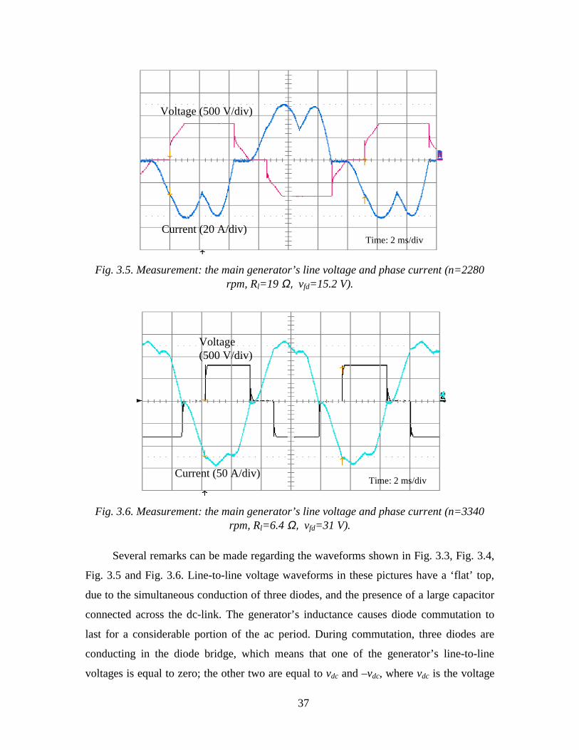
Fig. 3.5. Measurement: the main generator’s line voltage and phase current (n=2280 rpm,
Rl=19 Ω, vfd=15.2 V). 37
Fig. 3.6. Measurement: the main generator’s line voltage and phase current (n=3340 rpm,
Rl=6.4 Ω, vfd=31 V). 37
Fig. 3.7. Switching model simulation: the exciter’s line-to-line voltage and phase current
(n=3340 rpm, Rl=6.4 Ω, vfd=33 V). 38
Fig. 3.8. Switching model simulation: the main generator’s field voltage at exciter’s field
voltage step from 0 V to 47.5 V (n=4000 rpm, Rl=4.27 Ω). 39
Fig. 3.9. Switching model simulation: the main generator’s phase voltage and phase
current (n=2280 rpm, Rl=19 Ω, vfd=16 V). 41
Fig. 3.10. Switching model simulation: the main generator’s phase voltage and phase
current (n=3340 rpm, Rl=6.4 Ω, vfd=33 V). 41
Fig. 3.11. Switching model simulation: the exciter’s phase voltage and phase current
(n=3340 rpm, Rl=6.4 Ω, vfd=33 V). 42
Fig. 3.12. Switching model simulation: the main generator’s steady state armature d-axis
voltage and current. 43
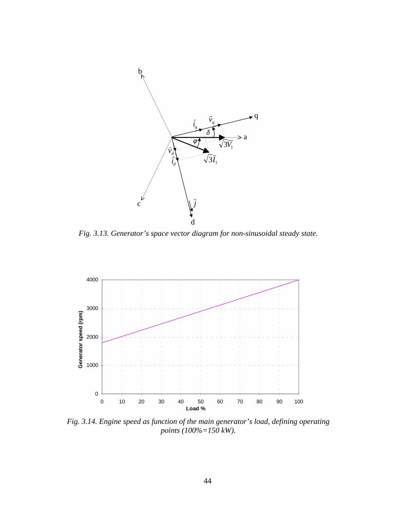
Fig. 3.13. Generator’s space vector diagram for non-sinusoidal steady state. 44
Fig. 3.14. Engine speed as function of the main generator’s load, defining operating
points (100%=150 kW). 44
Fig. 3.15. Variation of φ with the operating point. 45

x
Fig. 3.16. Variation of kv with the operating point. 47
Fig. 3.17. Variation of ki with the operating point. 47
Fig. 4.1. Generator/rectifier space vector diagram. 51
Fig. 4.2. Block diagram of the average model. 53
Fig. 4.3. Switching model simulation: the main generator’s field voltage at the exciter’s
field voltage step from 0 V to 47.5 V (n=4000 rpm, Rl=4.27 Ω). 57
Fig. 4.4. Average model simulation: the main generator’s field voltage at the exciter’s
field voltage step from 0 V to 47.5 V (n=4000 rpm, Rl=4.27 Ω). 57
Fig. 4.5. Measurement: dc-link voltage and the exciter’s field current at the exciter’s field
voltage step from 0 V to 8.5 V (n=3050 rpm, Rl=18.75 Ω). 58
Fig. 4.6. Switching model simulation: dc-link voltage and the exciter’s field current at the
exciter’s field voltage step from 0 V to 7 V (n=3050 rpm, Rl=18.75 Ω). 59
Fig. 4.7. Average model simulation: dc-link voltage and the exciter’s field current at the
exciter’s field voltage step from 0 V to 7 V (n=3050 rpm, Rl=18.75 Ω). 59
Fig. 4.8. Measurement: dc-link voltage and the exciter’s field current at the exciter’s field
current step from 0.34 A to 0 A (n=3050 rpm, Rl=18.75 Ω.). 60
Fig. 4.9. Switching model simulation: dc-link voltage and the exciter’s field current at the
exciter’s field current step from 0.38 A to 0 A (n=3050 rpm, Rl=18.75 Ω). 60
Fig. 4.10. Average model simulation: dc-link voltage and the exciter’s field current at the
exciter’s field current step from 0.38 A to 0 A (n=3050 rpm, Rl=18.75 Ω). 61
Fig. 4.11. Measurement: dc-link voltage and the exciter’s field current at resistive load
step from 12.5 Ω to 6.25 Ω (n=3100 rpm, vfd=11.6 V). 62
Fig. 4.12. Switching model simulation: dc-link voltage and the exciter’s field current at
resistive load step from 12.5 Ω to 6.25 Ω (n=3100 rpm, vfd=11.6 V). 62
Fig. 4.13. Average model simulation: dc-link voltage and the exciter’s field current at
resistive load step from 12.5 Ω to 6.25 Ω (n=3100 rpm, vfd=11.6 V). 63

xi
Fig. 4.14. (a) measurement, (b) average model simulation: dc-link voltage in transient
following disconnection of 19 Ω resistive dc load (n=2000 rpm, vfd=3.4 V in (a),
vfd=1.85 V in (b)). 63
Fig. 4.15. (a) measurement, (b) average model simulation: dc-link voltage in transient
following disconnection of 19 Ω resistive dc load (n=3700 rpm, vfd=2.8 V in (a),
vfd=2.03 V in (b)). 64
Fig. 4.16. Diode rectifier’s efficiency variation with load. 67
Fig. 4.17. Magnitude of the exciter’s field voltage-to-dc-link voltage transfer function
with current source load, at two different operating points. 84
Fig. 4.18. Phase of the exciter’s field voltage-to-dc-link voltage transfer function with
current source load, at two different operating points. 85
Fig. 4.19. Magnitude of the exciter’s field voltage-to-dc-link voltage transfer function at
3340 rpm, 105 kW, with different kinds of load. 88
Fig. 4.20. Phase of the exciter’s field voltage-to-dc-link voltage transfer function at 3340
rpm, 105 kW, with different kinds of load. 88
Fig. 4.21. The exciter’s field voltage-to-exciter’s field current transfer function at 3340
rpm, 105 kW current source load. 90
Fig. 4.22. The exciter’s field voltage-to-main generator’s field current transfer function at
3340 rpm, 105 kW current source load. 90
Fig. 5.1. The exciter’s field voltage-to-dc-link voltage transfer function at 3340 rpm and
105 kW current source load. 92
Fig. 5.2. Small-signal block diagram of the closed-loop system. 92
Fig. 5.3. Analog realization of a PI compensator. 94
Fig. 5.4. Loop gain with PI compensator (3340 rpm, 105 kW current source load). 95
Fig. 5.5. Average model simulation: dc-link voltage and the exciter’s field current at
resistive load step from 8.3 Ω to 12.5 Ω (n=2000 rpm, Vg=25 V). 96
xii
Fig. 5.6. Measurement: dc-link voltage and the exciter’s field current at resistive load step
from 8.3 Ω to 12.5 Ω (n=2000 rpm, Vg=25 V). 96
Fig. 5.7. Average model simulation: dc-link voltage and the exciter’s field current at
resistive load step from 8.3 Ω to 12.5 Ω (n=3800 rpm, Vg=15 V). 97
Fig. 5.8. Measurement: dc-link voltage and the exciter’s field current at resistive load step
from 8.3 Ω to 12.5 Ω (n=3800 rpm, Vg=15 V). 97
Fig. 5.9. Illustration for instability problem. 98
Fig. 5.10. Magnitude of the generator’s output impedance (in open and closed loop) and
the inverter’s input impedance (3340 rpm, 105 kW current source load). 99
Fig. 5.11. Loop gain with four-pole, three-zero compensator (3340 rpm, 105 kW current
source load). 101
Fig. 5.12. Generator’s closed loop output impedance with four-pole, three zero
compensator (3340 rpm, 105 kW current source load). 102
Fig. 5.13. Multiple-pole, multiple-zero compensators’ transfer function’s magnitudes. 103
Fig. 5.14. Loop gain with five-pole, three-zero compensator (3340 rpm, 105 kW current
source load). 104
Fig. 5.15. Generator’s closed loop output impedance with five-pole, three zero
compensator (3340 rpm, 105 kW current source load). 104
Fig. 5.16. Analog realization of a five-pole, three-zero compensator. 105
Fig. 5.17. Average model simulation: the dc-link voltage and exciter’s field current for a
resistive load step from 8.3 Ω to 12.5 Ω (n=2000 rpm, Vg=25 V). 107
Fig. 5.18. Measurement: the dc-link voltage and exciter’s field current for a resistive load
step from 8.3 Ω to 12.5 Ω (n=2000 rpm, Vg=25 V). 107
Fig. 5.19. Average model simulation: the dc-link voltage and exciter’s field current for a
resistive load step from 8.3 Ω to 12.5 Ω (n=3800 rpm, Vg=15 V). 108
Fig. 5.20. Measurement: the dc-link voltage and exciter’s field current for a resistive load
step from 8.3 Ω to 12.5 Ω (n=3800 rpm, Vg=15 V). 108

xiii
Fig. 5.21. Average model simulation: the dc-link voltage and exciter’s field current for a
resistive load step from 12.5 Ω to 8.3 Ω (n=2000 rpm, Vg=25 V). 109
Fig. 5.22. Measurement: the dc-link voltage and exciter’s field current for a resistive load
step from 12.5 Ω to 8.3 Ω (n=2000 rpm, Vg=25 V). 109
Fig. 5.23. Average model simulation: the dc-link voltage and exciter’s field current for a
resistive load step from 12.5 Ω to 8.3 Ω (n=3800 rpm, Vg=15 V). 110
Fig. 5.24. Measurement: the dc-link voltage and exciter’s field current for a resistive load
step from 12.5 Ω to 8.3 Ω (n=3800 rpm, Vg=15 V). 110
Fig. 5.25. Measurement: the dc-link voltage and exciter’s field current at step in the
inverter’s resistive three-phase load from 18.8 kW to 12.8 kW (n=3000 rpm, Vg=35
V). 111
Fig. 5.26. Measurement: the dc-link voltage and exciter’s field current at step in the
inverter’s resistive three-phase load from 12.8 kW to 18.8 kW (n=3800 rpm, Vg=35
V). 112

xiv
List of Tables
Table 2.1. Measured exciter’s parameters. 32
Table 4.1. Values of kv, ki and φ used for verification of the average model. 56
Table 4.2. Poles and zeros of efdadc vv ~/~ transfer function at 3340 rpm, 105 kW current
source load. 86
Table 4.3. Poles and zeros of efdadc vv ~/~ transfer function at 3340 rpm, 105 kW resistive
load. 89

1
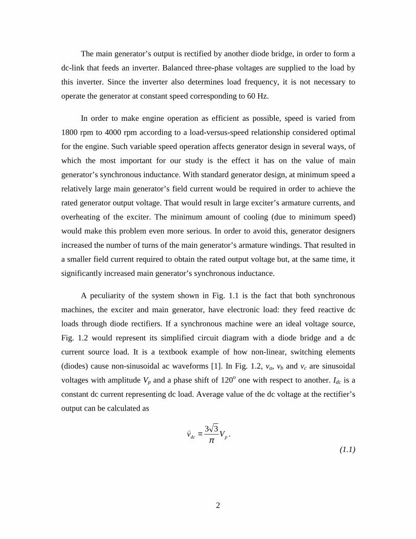
Chapter 1. Introduction
1.1. Motivation for this work and state of the art
This work was motivated by the need to study dynamics and control design of the
system whose block diagram is shown in Fig. 1.1. It is a 150 kW generator set with
inverter output, in which a natural gas engine drives a synchronous generator (which,
throughout this text, will also be referred to as main generator). Field voltage is provided
to the main generator by means of a separate, smaller synchronous machine, an exciter.
The exciter is constructed with field winding on the stator and armature winding on the
rotor; that makes it possible to rectify the exciter’s armature ac voltages by a rotating
diode bridge, and connect the rectifier’s output directly to the field winding of the main
generator.
EXCITER GENERATOR
RECTIFIER vdc
INVERTER
vfd
ENGINE LOAD
Modeled Subsystem
Fig. 1.1. Block diagram of the studied system.
2
The main generator’s output is rectified by another diode bridge, in order to form a
dc-link that feeds an inverter. Balanced three-phase voltages are supplied to the load by
this inverter. Since the inverter also determines load frequency, it is not necessary to
operate the generator at constant speed corresponding to 60 Hz.
In order to make engine operation as efficient as possible, speed is varied from
1800 rpm to 4000 rpm according to a load-versus-speed relationship considered optimal
for the engine. Such variable speed operation affects generator design in several ways, of
which the most important for our study is the effect it has on the value of main
generator’s synchronous inductance. With standard generator design, at minimum speed a
relatively large main generator’s field current would be required in order to achieve the
rated generator output voltage. That would result in large exciter’s armature currents, and
overheating of the exciter. The minimum amount of cooling (due to minimum speed)
would make this problem even more serious. In order to avoid this, generator designers
increased the number of turns of the main generator’s armature windings. That resulted in
a smaller field current required to obtain the rated output voltage but, at the same time, it
significantly increased main generator’s synchronous inductance.
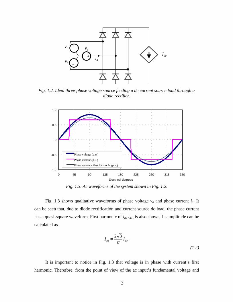
A peculiarity of the system shown in Fig. 1.1 is the fact that both synchronous
machines, the exciter and main generator, have electronic load: they feed reactive dc
loads through diode rectifiers. If a synchronous machine were an ideal voltage source,
Fig. 1.2 would represent its simplified circuit diagram with a diode bridge and a dc
current source load. It is a textbook example of how non-linear, switching elements
(diodes) cause non-sinusoidal ac waveforms [1]. In Fig. 1.2, va, vb and vc are sinusoidal
voltages with amplitude Vp and a phase shift of 120o one with respect to another. Idc is a
constant dc current representing dc load. Average value of the dc voltage at the rectifier’s
output can be calculated as
pdc Vvπ
33=.
(1.1)
3
Idc
va
vc
vb
+
+
+ ia
Fig. 1.2. Ideal three-phase voltage source feeding a dc current source load through adiode rectifier.
-1.2
-0.6
0
0.6
1.2
0 45 90 135 180 225 270 315 360
Electrical degrees
Phase voltage (p.u.)
Phase current (p.u.)
Phase current's first harmonic (p.u.)
Fig. 1.3. Ac waveforms of the system shown in Fig. 1.2.
Fig. 1.3 shows qualitative waveforms of phase voltage va and phase current ia. It
can be seen that, due to diode rectification and current-source dc load, the phase current
has a quasi-square waveform. First harmonic of ia, ia1, is also shown. Its amplitude can be
calculated as
dca IIπ
321 = .
(1.2)
It is important to notice in Fig. 1.3 that voltage is in phase with current’s first
harmonic. Therefore, from the point of view of the ac input’s fundamental voltage and
4
current harmonics, an ideal diode rectifier with a current source dc load behaves like a
nonlinear resistor.
Idc
va
vc
vb
+
+
+ ia
Ll
Ll
Ll
B
A
C
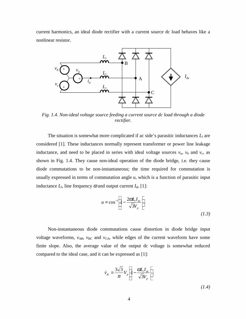
Fig. 1.4. Non-ideal voltage source feeding a current source dc load through a dioderectifier.
The situation is somewhat more complicated if ac side’s parasitic inductances Ll are
considered [1]. These inductances normally represent transformer or power line leakage
inductance, and need to be placed in series with ideal voltage sources va, vb and vc, as
shown in Fig. 1.4. They cause non-ideal operation of the diode bridge, i.e. they cause
diode commutations to be non-instantaneous; the time required for commutation is
usually expressed in terms of commutation angle u, which is a function of parasitic input
inductance Ll, line frequency ω and output current Idc [1]:
−= −
p
dcl
V
ILu
3
21cos1 ω
.
(1.3)
Non-instantaneous diode commutations cause distortion in diode bridge input
voltage waveforms, vAB, vBC and vCA, while edges of the current waveform have some
finite slope. Also, the average value of the output dc voltage is somewhat reduced
compared to the ideal case, and it can be expressed as [1]:
−=
p
dclpdc
V
ILVv
31
33 ωπ
.
(1.4)

5
Expression (1.4) is valid only if 3
π<u ; for cases in which 3
π≥u , expressions
similar to (1.4) can be found [1].
It needs to be understood that (1.1) and (1.2) describe an ideal operation of the
diode rectifier in an average sense: they express average dc output voltage by means of
input ac peak voltage, and fundamental harmonic of input ac current by means of the
output dc current. These expressions do not contain any information about the voltage
ripple at the dc side and the current’s higher harmonics at the ac side.
A synchronous generator is never an ideal voltage source, and it is even less so if it
is characterized by a large value of synchronous inductance. If it is connected to a diode
rectifier, inductance Ll from Fig. 1.4 is of the order of magnitude of the generator’s
synchronous inductance. Therefore, it can be expected that the exciter’s and the main
generator’s ac terminal voltage and current waveforms will be heavily distorted [2]-[7].
Fig. 1.5 shows measured waveforms of the system from Fig. 1.1 and can serve as an
example of such distortion. It can be seen that the main generator’s line-to-line voltage is
a quasi-square wave, and the current is also far from being sinusoidal.
Voltage(500V/div)
Current(50A/div)
Fig. 1.5. Main generator’s line-to-line voltage and phase current with a 100 kW resistiveload connected to the dc-link (time scale: 2 ms/div).
Similarly, a dc load is never an ideal dc current source. For a heavily inductive dc
load, like the main generator’s field winding that loads the exciter in Fig. 1.1, the current
6
source approximation is very close to the actual situation. For the main generator, which
has a large dc-link capacitor and an inverter as a load, that is not the case.
For the above reasons, operation of the system shown in Fig. 1.1 cannot be
described with analytical expressions such as (1.1) (or (1.3)) and (1.2). Moreover, even
though it is not obvious from Fig. 1.5, there is a phase-shift between the first harmonics
of the phase voltage and the phase current. Therefore, as a result of the non-ideal
operation of the diode-bridge, the generator will behave as if some reactive load were
connected to its terminals.
Some design aspects relative to the system shown in Fig. 1.1 (e.g., design of
protection measures at the dc-link) require large-signal, time-domain simulation results.
Simulation of the system’s switching model can provide these results, but is extremely
time- and memory consuming (time-constants of the system are of the order of magnitude
of hundreds of milliseconds, and the maximum simulation time-step needs to be kept well
below the switching ripple period, i.e. on the order of millisecond). Therefore, from the
point of view of large signal analysis, the need for an ‘average’ model of the system can
be anticipated. Such a model would describe dynamic behavior of the system without
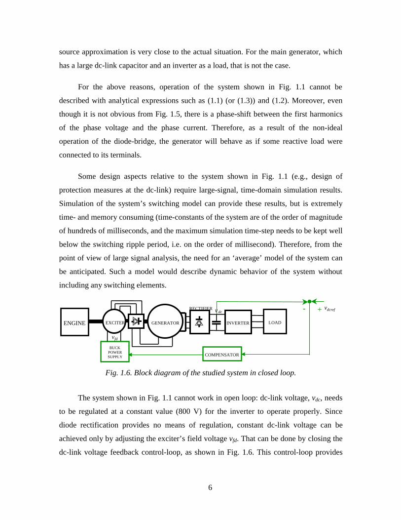
including any switching elements.
EXCITER GENERATOR
RECTIFIER vdc
COMPENSATOR
BUCKPOWERSUPPLY
vdcref+-
INVERTER
vfd
ENGINE LOAD
Fig. 1.6. Block diagram of the studied system in closed loop.
The system shown in Fig. 1.1 cannot work in open loop: dc-link voltage, vdc, needs
to be regulated at a constant value (800 V) for the inverter to operate properly. Since
diode rectification provides no means of regulation, constant dc-link voltage can be
achieved only by adjusting the exciter’s field voltage vfd. That can be done by closing the
dc-link voltage feedback control-loop, as shown in Fig. 1.6. This control-loop provides

7
regulation of the inverter’s input voltage, but also plays an important role in impedance
matching between the generator and inverter, thus assuring system stability.
In order to design the compensator in Fig. 1.6, it is necessary to have a good small-
signal model representing the system’s dynamic behavior. A three-phase, salient pole,
wound field synchronous generator is characterized by relatively complex dynamics. In
order to describe properly its electrical behavior, it is necessary to deal with at least a
third order system, which becomes fifth (or higher) order if there are damper windings
present in the machine [8], [9]. These high-order models contain complete information
about the generator’s dynamics, but are often quite demanding to use, both from
parameters identification and computational burden point of view. In particular, for the
generator’s control-loop design, it is a common practice to model a generator as a first-
order system [11], [12]. For that simplification to be legitimate, two assumptions need to
be true. First, the generator has to behave as a good voltage source; i.e. its synchronous
impedance needs to be small. Second, the generator must operate at constant speed. Both
assumptions are normally true for large generators used in power generation plants.
However, the system shown in Fig. 1.1 is characterized by variable speed and the large
main generator’s synchronous impedance. Also, if the exciter’s field voltage is
considered input, and the dc-link voltage output variable, the overall order of the system
is eight. Therefore, it can be suspected that the above-mentioned, single-pole generator
model would hardly be appropriate. The presence of diode rectifiers makes modeling of
the system even more difficult. The diode’s switching behavior causes the system to be
time-discontinuous, and therefore impossible to linearize. Moreover, it is not clear how to
model the effect of the distorted generator’s ac waveforms.
The above–mentioned, design–related requirements for transient and small–signal
representation of the system’s behavior define the goal of this work. It consists of
developing a model of the system with the following properties:
• Accurate dynamic representation of the generator, load and effects of non-ideal
operation of diode rectifier;
8
• Suitability for time domain simulations, with emphasis on efficient use of CPU
time and computer memory; and
• Suitability for small-signal analysis and application to control design.
The following section is a short overview of the topics covered in the body of the
text.
1.2. Thesis outline
Chapter 2, Synchronous Generator Dynamic Modeling, starts with a summary of
synchronous machine’s dynamic model development. This model has been known for
more than half a century, and that is why its development is not carried out in a detailed
manner; only the main assumptions and results are presented. During the work that
resulted in this thesis, a considerable amount of time and effort was spent on the
parameter identification problem, particularly for the exciter. That is why this chapter
also contains a brief description of the parameter identification process. Following that is
a section dedicated to the review of the generator’s steady state operation, and a short
section on how the generator’s model can be implemented in a simulation software like
PSpice.
In Chapter 3, results obtained by simulating the “modeled subsystem” from Fig. 1.1
are presented and compared to the measurement results. This is referred to as the
“switching model” of the system, since it includes switching elements (diodes), and
therefore describes the system as it actually operates. Results obtained with the switching
model simulations are discussed, and the basis is set for the development of the average
model.
Chapter 4, Average Model, is the most innovative part of this work. Based on
conclusions regarding the switching model of the system, this chapter shows how a
system, consisting of a synchronous generator, a diode bridge rectifier and some reactive

9
dc load, can be modeled in a simplified way. This is referred to as the “average model” of
the system. The average model preserves all of the system’s relevant dynamic
information, but it does not include any switching elements. That makes it particularly
useful for linearization and control-loop design. Assumptions for the development of the
average model are presented, and derivation of the model’s equations is carried out. The
average model is then verified through comparison with the switching model and
measurement results. Since the average model equations are non-linear, it is shown how
they can be linearized and how the corresponding state-space representation of the system
can be found. Finally, a discussion on model’s validity is included.
Chapter 5 contains dc-link voltage control-loop design procedure. It is based on the
exciter’s field voltage-to-dc-link voltage transfer function obtained with the average
model developed in Chapter 4. A design procedure for a PI compensator is given, and
transient simulation and measurement results with resistive load at the dc-link are shown.
Unstable operation of this compensator with an inverter load due to poor impedance
matching between different parts of the system is discussed, and the need for a higher-
order dynamic compensator is justified. A five-pole, three-zero compensator is found to
be satisfactory, and its design process is carried out. Validity of this compensator is
confirmed through simulation and measurement results of transient operation with
resistive and inverter load at the dc-link.
Chapter 6 concludes the thesis by summarizing its most important results.

10
Chapter 2. Synchronous
Generator Dynamic Modeling
2.1. Synchronous generator model in rotor reference
frame
It was explained in the introductory chapter why a first-order synchronous machine
model would not be appropriate for the application that motivated the work presented in
this thesis. The purpose of this section is to introduce a detailed synchronous generator
model, which takes into account all relevant dynamic phenomena occurring in the
machine. Since this model has been widely known since 1930s, only the main
assumptions and results will be presented.

11
2.1.1. Assumptions for model development
A three-phase, wound-field synchronous generator has three identical armature
windings symmetrically distributed around the air-gap, and one field winding. One or
more damper windings can also be present and, for our convenience in this section, we
will assume that one damper winding is present in each machine’s axis. Normally,
armature windings are placed on the stator, and field and damper windings on the rotor.
However, there are cases, such as the exciter in Fig. 1.1, when armature windings are
placed on the rotor and field winding on the stator (the exciter has no damper windings).
This does not affect the machine modeling approach at all, since only relative motion
between the stator and rotor windings is important. Therefore, throughout this text, when
we refer to ‘rotor windings’, we will always imply the field (and damper, if existent)
winding placed at the opposite side of the air gap with respect to the three-phase armature
windings.
Several assumptions are needed in order to simplify the actual synchronous
machine and make the model development less tedious [9]:
1. It is assumed that every winding present in the machine produces a sinusoidal
MMF along the air gap, which, for phase a, can be expressed as
Θ= saa
Pγθ2
sin , where P represents the machine’s number of poles, and γs
stands for the stator’s angular coordinate;
2. Iron permeability in the machine is assumed to be infinite. This is equivalent to
neglecting all effects due to magnetic saturation, and flux fringing;
3. Rotor construction is assumed to be the only factor contributing to magnetic
asymmetry in the machine. Effects of the stator or rotor slots can be taken into
account by Carter’s factor. This assumption results in approximating the
magnetic conductivity function as )cos(20 sPγλλλ −= , where λ0 and λ2
depend on the geometry of the air gap; and

12
4. Local value of magnetic flux density B is obtained by multiplying local values
of MMF and magnetic conductivity. The third harmonic of the magnetic flux
density resulting from this multiplication is neglected, in accordance with
assumption 1.
Errors introduced by these assumptions are normally small enough to be negligible,
particularly from the point of view of the machine’s dynamic performance.
2.1.2. Development of the model’s equations and equivalent
circuit
A synchronous machine can be described by a system of n+1 equations, n of which
are electrical and one of which is mechanical. The number n of electrical equations is
equal to the number of independent electrical variables necessary to describe the
machine. These variables can be either currents or flux linkages. Currents are chosen to
be the independent variables in this thesis.
Electrical equations are obtained by writing Kirchoff’s voltage law for every
winding, i.e. by equating the voltage at the winding’s terminal to the sum of resistive and
inductive voltage drops across the winding [8], [9]. Note that damper windings, if
present, are always short circuited. Therefore, their terminal voltage is equal to zero.
In order to correctly calculate the inductive voltage drop across a winding, total
magnetic flux linked with the winding needs to be evaluated. That is achieved by means
of an inductance matrix, which relates all windings’ flux linkages to all windings’
currents. When that is done for a salient-pole synchronous machine, an inductance matrix
dependent on the rotor position is obtained. This dependence is due to the magnetic
asymmetry of the rotor: because of the way the rotor of a salient pole machine is shaped,
there exists a preferable magnetic direction. This direction coincides with the direction of
the flux produced by the field winding, and is defined as machine’s d axis. The machine’s
q axis is placed at 90 electrical degrees (in a counterclockwise direction) with respect to

13
the machine’s d axis. Then, the rotor position can be expressed by means of an angle,
named θ, between the magnetic axis of the armature’s phase a and the rotor’s q axis.
Dependence of the inductance matrix on the rotor position represents the main
difficulty in modeling the synchronous machine. A solution to this problem is to change
the reference system, or frame, in which the machine’s electrical and magnetic variables
are expressed. So far, the reference frame intuitively used was the so-called stationary, or
stator, or abc reference frame. In it, variables are expressed as they can actually be
measured in the machine, but the machine parameters are time variant (since θ is a
function of time). It can be shown that the only reference frame that provides constant
machine parameters is the rotor, or dq, reference frame. In it, all variables are expressed
in a form in which a hypothetical observer placed on the rotor would measure them.
Transformation from the abc to the dq reference frame is given by the following
transformation matrix:
+
−
+
−
=
3
2cos
3
2coscos
3
2sin
3
2sinsin
3
2πθπθθ
πθπθθT .
(2.1)
Inverse transformation (from the dq to the abc reference frame) is then given by
+
+
−
−=
3
2cos
3
2sin
3
2cos
3
2sin
cossin
3
2
πθπθ
πθπθθθ
invT .
(2.2)
In (2.1) and (2.2), θ is calculated as
0
0
)()( θξξωθ += ∫t
dt ,
(2.3)
14
where ω represents the rotor’s (electrical) speed.
Therefore, any set of three-phase variables fa, fb and fc expressed in the abc
reference frame can be transformed in dq reference frame variables fd and fq by
multiplying them by T:
=
c
b
a
q
d
f
f
f
f
fT .
(2.4)
Vice versa:
=
q
d
inv
c
b
a
f
f
f
f
f
T .
(2.5)
Note that transformation of the variables, as defined by (2.1) and (2.2), preserves
total system power: in every time instant, power in the abc reference frame is equal to the
power in the dq reference frame.
Another comment needs to be made regarding zero variables, which generally must
be taken into account when variables are transformed into the rotor reference frame. In
our case, with a Y-connected generator without neutral connection, zero variables are
always equal to zero, and are therefore excluded from representation.
When the machine’s electrical equations are transformed from the abc to the dq
reference frame, they assume the following form:
• Armature equations
dt
di
dt
di
dt
diiv kdfdd
qdd mdmdmdlss LL)LL(R +++−−−= ωλ ,
(2.6)
dt
di
dt
diiv kqq
dqq mqmqlss L)LL(R ++−+−= ωλ ,
(2.7)

15
where
)(L)LL( mdmdls kdfddd iii +++−=λ ,
(2.8)
kqqq ii mqmqls L)LL( ++−=λ ;
(2.9)
• Field equation
dt
di
dt
di
dt
diiv kdfdd
fdfd mdmdlfdmdfd L)LL(LR +++−= ;
(2.10)
• Damper winding equations
dt
di
dt
di
dt
dii kdfddkd )LL(LLR0 mdlkdmdmdkd +++−= ,
(2.11)
dt
di
dt
dii kqq
mqkq )LL(LR0 mqlkqkq ++−= .
(2.12)
Parameters and variables in the above equations have the following meanings:
• ω: rotor speed;
• vd: armature d axis terminal voltage;
• vq: armature q axis terminal voltage;
• id: armature d axis terminal current;
• iq: armature q axis terminal current;
• vfd: field winding terminal voltage (reflected to the stator);
• i fd: field winding terminal current (reflected to the stator);
• ikd: d axis damper winding current (reflected to the stator);
• ikq: q axis damper winding current (reflected to the stator);

16
• λd: total armature flux in d axis;
• λq: total armature flux in q axis;
• Rs: armature phase resistance;
• Lls: armature phase leakage inductance;
• Lmd: d axis coupling inductance;
• Rfd: field winding resistance (reflected to the stator);
• Llfd: field winding leakage inductance (reflected to the stator);
• Rkd: d axis damper wining resistance (reflected to the stator);
• Llkd: d axis damper winding leakage inductance (reflected to the stator);
• Lmq: q axis coupling inductance;
• Rkq: q axis damper winding resistance (reflected to the stator);
• Llkq: q axis damper winding leakage inductance (reflected to the stator).
Equations (2.6)-(2.12) describe the synchronous generator’s equivalent circuit in
the rotor reference frame shown in Fig. 2.1.
Several comments can be made regarding this equivalent circuit:
• D and q axis equivalent circuits are similar to a transformer equivalent circuit: in
each of them, several windings, each characterized by some resistance and
leakage inductance, are coupled through a mutual coupling inductance. The
difference, compared to the transformer case, is that, while a transformer
equivalent circuit is an ac circuit, here, when the generator is operating in
sinusoidal steady state, all voltages, currents and flux linkages are dc.
• Even though armature windings are now represented in the rotor reference frame,
and there are no time-variant inductances, the fact that armature windings are
magnetically coupled is taken into account by presence of cross-coupling terms in
the d and q axis’s equivalent circuit’s armature branch. For each axis, that term is

17
equal to the product of rotor speed and total flux linked with armature winding of
the other axis.
vd
id RsLls
Lmd
Rfd
Llfd
Rkd
Llkd
vfd
+ωλ
q
+
vq
iq Rs Lls
Lmq
Rkq
Llkq
+ωλ
d
+
+
Fig. 2.1. Synchronous generator’s equivalent circuit in rotor reference frame.
• If a machine (such as the exciter) has no damper windings, the equivalent circuit
can be easily adapted by removing from it the branches representing damper
windings. The rest of the circuit remains unchanged.
• All rotor parameters are reflected to armature. Therefore, when this circuit is used
for simulation, and actual values of rotor variables are of interest, the turns ratio
between the rotor and armature needs to be taken into account.
This equivalent circuit describes a synchronous generator electrically. The
mechanical variable is represented by rotor speed ω, and the mechanical equation of the
system is needed in order to complete the model. This equation relates the external torque
applied to the generator’s shaft to the electromagnetic torque that the machine develops
internally. However, for the purpose of this thesis, the mechanical equation of the system
is not considered, i.e. rotor speed is assumed to be known. The reason for that is the fact

18
that our interest consists primarily in describing electrical behavior of the generator
loaded with a diode rectifier and a dc reactive load. To do that, it is legitimate to assume
constant speed, since electrical transients in the machine can be considered much faster
than mechanical transients (which involve the engine’s dynamics and inertia and the
generator’s inertia). However, the main results of this work (the average model described
in Chapter 4) will be verified at different values of rotor speed, in order to assure their
validity.
With the above considerations, rotor speed ω is not a variable, but a parameter of
the system. That causes (2.6)-(2.12) to be a set of linear differential equations.
2.1.3. Sinusoidal steady state operation
If a generator operates in sinusoidal steady state, phase voltages can be written in
the abc reference frame as
vpa Vv θcos= ,
(2.13)
−=
3
2cos
πθvpb Vv ,
(2.14)
+=
3
2cos
πθvpc Vv ,
(2.15)
where
0vvv t θωθ += .
(2.16)
In steady state, obviously, ωv=ω. However, in order to reach a steady state, the
generator must go through a transient during which the rotor electrical speed can be

19
different from the terminal voltage’s angular frequency. That is the transient which
allows the machine to reach the steady state value of rotor angle δ, defined as the
displacement of the rotor referenced to the maximum positive value of the fundamental
component of the terminal voltage of phase a. It can be expressed, in radians, as
∫ −+−=−=t
vvv d0
)0()0())()(( θθξξωξωθθδ .
(2.17)
Then, after applying (2.1) to (2.13)-(2.15), in the dq reference frame we have
δθθ sin2
3)sin(
2
3pvpd VVv =−= ,
(2.18)
δθθ cos2
3)cos(
2
3pvpq VVv =−= .
(2.19)
Expressions (2.18) and (2.19) suggest that, in order to be able to represent dq
reference frame variables and ac space vectors in the same diagram, a complex
(Gaussian) plane be associated with the machine’s ‘physical’ dq plane. The Gaussian
plane’s real axis is aligned with the machine’s q axis, and the Gaussian plane’s imaginary
axis is aligned with machine’s d axis. It can then be written
)(3
1dq vjvV += .
(2.20)
In (2.20), V represents the space vector associated to voltages va, vb and vc defined
by (2.13)-(2.15), and j represents the unity vector in the direction of imaginary axis.
Remember that the length of a space vector is assumed to be equal to the variable’s rms
value. Fig. 2.2 shows the position of the dq reference frame and space vector V3 at
time t=0. Space vector V3 and dq reference frame rotate at constant speed ω in a

20
counterclockwise direction, and the instantaneous values of va, vb and vc are obtained as
projections of V2 onto axes a, b and c, which are still.
a
c
b
V3
δ
d
q
vd
vq
j
I3
iq
id
φ
Fig. 2.2. Generator’s space vector diagram for sinusoidal steady state operation.
Space vector I3 , representing phase currents, is shifted by load angle φ with
respect to V . The instantaneous values of phase currents in the abc reference frame are
obtained as projections of I2 onto axes a, b and c, and (constant) values of phase
currents in the rotor reference frame are obtained as projections of the current space
vector onto the d and q axis, which yields
)sin(2
3 φδ += pd Ii ,
(2.21)
)cos(2
3 φδ += pq Ii ,
(2.22)
where Ip stands for peak phase current.
21
2.1.4. Model implementation in a simulation software
Synchronous generator equivalent circuit in the rotor reference frame, shown in
Fig. 2.1, is very convenient to simulate with any software that allows schematic
descriptions of electric circuits, since only resistors, inductors and current dependent
voltage sources need to be implemented. PSpice [10] was used for all simulation results
in this thesis. Implementation of the circuit is straightforward, and only a few details will
be given some attention in this section
Cross-coupling terms in armature branches contain total armature flux in d and q
axis, given by (2.8) and (2.9). It is evident that these terms can be implemented using
current-dependent voltage sources.
The generator model is implemented in the dq reference frame, but it is usually of
practical interest to a have three-phase generator’s output terminals available in a
simulation process. That can be done by implementing the generator’s output with three
current-dependent current sources (Fig. 2.3), which generate currents in the abc reference
frame by calculating them from armature currents in the dq reference frame as
=
q
d
inv
c
b
a
i
i
i
i
i
T .
(2.23)
GENERATORMODEL IN DQREFERENCE
FRAME
THREE-PHASE LOAD
IN ABCREFERENCE
FRAME
ia
ib
ic
+ vdid
+ vqiq
+
+
+
va
vb
vc
Fig. 2.3. Implementation of generator’s three-phase output.
From the principle of duality, the generator model in the rotor reference frame is
loaded with two voltage-dependent voltage sources (Fig. 2.3), representing the

22
generator’s armature voltages in dq reference frame, and calculated from the generator’s
armature voltages in the abc reference frame as
=
c
b
a
q
d
v
v
v
v
vT .
(2.24)
In order to be able to implement (2.23) and (2.24), rotor angle θ needs to be known.
It can be calculated from (2.3), with the rotor speed represented by a current source
charging a 1 F capacitor. Voltage across this capacitor is numerically equal to the rotor
angle θ. The initial angle θ0, if needed, can be implemented by an ideal dc voltage source
in series with the capacitor.
One last comment regarding the generator’s field voltage value. All rotor
parameters and variables in model equations are referred to armature. However, for
purposes of easy comparison of simulation with measurement results, it is convenient to
implement the field voltage source in the simulation process as it actually exists in a real
machine. To be able to do that, field-to-armature equivalent turns ratio t needs to be
known. The following relationships exist between the actual field winding variables and
field winding variables referred to armature (index ‘act’ denotes an actual field winding
variable, i.e. the variable as it can be measured at field winding terminals):
fdactfd tvv = ,
(2.25)
fdfdact tii = .
(2.26)
These relationships can be implemented as shown in Fig. 2.4.

23
GENERATORMODEL IN DQREFERENCE
FRAME
+tvfdact
ifd
+ti fdvfdact
Fig. 2.4. Implementation of generator’s field voltage.
2.2. Parameter identification
The synchronous generator equivalent circuit from Fig. 2.1 requires a large number
of machine’s parameters to be known. These parameters can be obtained from either the
generator’s design data or through measurements.
The two most common ways to measure a synchronous machine’s parameters are
short-circuit characteristics and standstill frequency response characteristics [8], [9], [13]-
[19]. Both of these methods are based on determining the machine’s parameters from the
following standard inductances and time-constants:
• D axis synchronous inductance Ld
mdlsd LLL += ;
(2.27)
• D axis transient inductance Ld’
lfdmd
lfdmdls
'd LL
LLLL
++= ;
(2.28)
• D axis subtransient inductance Ld’’
24
lkdlfdlkdmdlfdmd
lkdlfdmdls
''d LLLLLL
LLLLL
+++= ;
(2.29)
• Q axis synchronous inductance Lq
mqlsq LLL += ;
(2.30)
• Q axis subtransient inductance Lq’’
lkqmq
lkqmqls
''q LL
LLLL
++= ;
(2.31)
• D axis open circuit transient time constant T’do
fd
mdlfd'do R
LLT
+= ;
(2.32)
• D axis short circuit transient time constant T’d
fd
lsmd
lsmdlfd
'd R
LLLL
L
T+
+= ;
(2.33)
• D axis open circuit subtransient time constant T’’do
kd
lfdmd
lfdmdlkd
''do R
LLLL
L
T+
+= ;
(2.34)
• D axis short circuit subtransient time constant T’’d
kd
lslfdlsmdlfdmd
lslfdmdlkd
''d R
LLLLLLLLL
L
T++
+= ;
(2.35)

25
• Q axis open circuit subtransient time constant T’’qo
kq
mqlkq''qo R
LLT
+= ;
(2.36)
• Q axis short circuit subtransient time constant T’’q
kq
lsmq
lsmqlkq
''q R
LL
LLL
T+
+= .
(2.37)
Measurement of short-circuit characteristics requires measurement of the waveform
of the armature current immediately after a three-phase short circuit is performed at the
armature terminals. During the transient, the machine is rotating at a constant speed, and
field voltage is kept constant. From the measured armature current waveform, it is
possible to extract the values of Ld, Ld’’ , Td
’ and Td’’ , and from them to calculate the d
axis parameters. This method does not allow calculation of the parameters of the q axis.
Measurement of frequency response characteristics requires blocking the rotor in a
position in which its d (or q) axis is aligned with the flux produced by the armature
windings. With field winding shorted, frequency response is measured from the armature
terminals. The obtained Bode plots allow to determine Ld, Ld’’ , Lq, Lq
’’ , Td’, Tdo
’, Td’’ ,
Tdo’’ , Tq
’’ , Tqo’’ and, from them, all parameters of the d and q axes.
In a system like the one shown in Fig. 1.1, it is difficult to perform any of these
measurements. The reason for thist is that the exciter’s armature terminals and main
generator’s field terminals are not accessible (they rotate with the shaft). Since detailed
design data sheets were available for the main generator, all the main generator’s
parameters were extracted from these data sheets. In the exciter’s case, no reliable design
data sheets were available. Therefore, an exciter’s stator and rotor (without a shaft) were
obtained from the manufacturer, and some measurements, conceptually similar to
standstill frequency response measurements, were done.

26
2.2.1. Main generator
Design data sheets resulted in the following values of the main generator’s
parameters at 145oC:
• P= 4 poles;
• Rs=0.137 Ω;
• Lls=0.897 mH;
• Lmd=43.2 mH;
• Rfd=0.0266 Ω;
• Llfd=3.37 mH;
• Rkd=0.120 Ω;
• Llkd=0.164 mH;
• Lmq=20.8 mH;
• Rkq=0.120 Ω;
• Llkq=0.347 mH;
• t=0.098.
2.2.2. Exciter
The exciter is a machine without damper windings, and that makes measurements
of its parameters relatively easy. The parameters to be determined are Rs, Lls, Lmd, Lmq,
Rfd, Llfd and t. While Rs and Rfdact can be measured directly at the winding’s terminals,
Lls, Lmd, Lmq, Llfd and Rfd can be calculated using (2.27)-(2.33), once Ld, Ld’, T’
do, T’d and
Lq are measured.

27
Measurement of Ld and Ld’
Consider the exciter with the rotor blocked and windings positioned as
schematically shown in Fig. 2.5. With θ=0o, ω=0 rad/s, the transformation matrix is
−−
−=
6
1
6
1
3
22
1
2
10
T ,
(2.38)
while the inverse transformation matrix is
−
−−=
6
1
2
16
1
2
13
20
invT .
(2.39)
ccbb
aa
f1f1f2f2 dd
ii
vv
++
Fig. 2.5. Circuit for measurement of Ld and Ld’.
From Fig. 2.5, armature currents in the abc reference frame can be expressed as
ia=0, ib=i , ic=-i . Armature currents in the dq reference frame are easily calculated by
applying (2.4), which yields iid 2−= , iq=0. Then, if field winding terminals f1 and f2
are left open (ifd=0), equations (2.6)-(2.12) are reduced to

28
++=+−−=
dt
dii
dt
diiv s
ddsd )LL(R2)LL(R mdlsmdls ,
(2.40)
0=qv ,
(2.41)
dt
div d
fd mdL−= .
(2.42)
Once vd and vq are known, va, vb and vc can be found from (2.5), yielding
0=av ,
(2.43)
dt
diivv scb )LL(R mdls +−−=−= .
(2.44)
Finally, supply voltage v can be expressed from vb and vc:
++=−=
dt
diivvv sbc )LL(R2 mdls .
(2.45)
If v is a sinusoidal voltage source of frequency ωs, (2.45) can be rewritten in terms
of phasors as
[ ] [ ]dsmdlss LR2)LL(R2 ss jjI
V ωω +=++= ,
(2.46)
where Ld stands for the exciter’s d axis synchronous inductance. It is clear now that, by
measuring V , I and Rs, it is possible to determine the value of Ld.
It can be shown that, in the same conditions as above, except for field winding
terminals f1 and f2 being shorted instead of open (vfd=0), the following is valid if
Rfd<< ωsLlfd:

29
[ ]'ds
lfdmd
lfdmdlss LR2)
LL
LLL(R2 ss jj
I
V ωω +=
+
++≈ .
(2.47)
In this way, d axis transient inductance Ld’ can be found.
Measurement of T’do and T’
d
D axis time constants Tdo’ and Td
’ can be found from measurements performed at
the field winding terminals. The configuration shown in Fig. 2.6 is used. Remember that
time constants do not depend on whether they are referred to the rotor or to the armature.
Therefore, it is allowable to draw conclusions from the machine’s equations referred to
the armature, but to perform measurements at the actual field winding terminals.
ccbb
aa
f1f1
f2f2
dd
ii
vv++
Fig. 2.6. Circuit for measurement of Tdo’ and Td
’.
If the armature windings are left open, (2.10) immediately yields
dt
diiv )LL(R mdlfdfd ++= ,
(2.48)
or, written with phasors,
fdos ZjI
V =++= )LL(R mdlfdfd ω .
(2.49)

30
Then, as (2.32) suggests, the d-axis open-circuit transient time constant can be
found from the resistive and inductive part of fdoZ .
If the armature terminals are shorted, the assumption that Rs<<ωsLls needs to be
made in order to measure Td’. With va=vb=vc=vd=vq=0, and stator resistance Rs
neglected, (2.6)-(2.10) yield
fdd iimdls
md
LLL
+= ,
(2.50)
0=qi ,
(2.51)
dt
diiv fd
fdfd
+
++=lsmd
lsmdlfdfd LL
LLLR .
(2.52)
When (2.52) is written in terms of phasors, we obtain
fds ZjI
V =
+
++=lsmd
lsmdlfdfd LL
LLLR ω .
(2.53)
Then, as (2.33) suggests, d axis short-circuit transient time constant can be found
from the resistive and inductive part of fdZ .
Measurement of Lq
For measurement of the q axis parameters, the windings can still be positioned as in
Fig. 2.5, but the armature terminals need to be connected as shown in Fig. 2.7. It has no
importance, in this case, whether the field winding is left open or shorted, since no flux
produced by the armature links the field winding.

31
ccbb
aa
f1f1f2f2 dd
ii
vv++
Fig. 2.7. Circuit for measurement of q axis parameters.
With the connection as in Fig. 2.7, abc reference frame armature currents are
iia −= , iib 21= , iic 2
1= , which, by virtue of (2.4), yields id=0, iiq 2
3−= . Then, from
(2.6) and (2.7), armature voltages in rotor reference frame can be found as
0=dv ,
(2.54)
++=+−−=
dt
dii
dt
diiv qqq )LL(R
2
3)LL(R mqlssmqlss .
(2.55)
From (2.54) and (2.55), by using (2.5), the armature voltages in the abc reference
frame are
dt
diiva )LL(R mqlss ++= ,
(2.56)
++−==
dt
diivv cb )LL(R
2
1mqlss .
(2.57)
Since v=va-vb, it can be written (in phasor terms)
[ ] )LR(23
)LL(R23
qsmqlss ss jjI
V ωω +=++= ,
(2.58)

32
which makes it clear that Lq can be found after IV , and Rs are measured.
Note that where a factor of two was present in (2.46), expression (2.58) has a factor
of 3/2. That can be intuitively explained by the way the armature phases are connected in
Fig. 2.5 and Fig. 2.7.
The above-described measurements were performed at the available exciter’s stator
and rotor. Since there were no shaft and bearings, uniformity of the air gap was assured
by inserting transformer paper between stator and rotor. Resistances were measured at dc
and 25ºC, and ac measurements were performed at three different frequencies, in order to
check for the effects of iron eddy currents. Since there is no standard way of dividing Ld
into its two components, Lls and Lmd, it is assumed that Lls represents 5% of the value of
Ld. Table 2.1 summarizes the measurement results. It was found that eddy currents had
no influence, since the measurements at all three frequencies gave very similar values.
Table 2.1. Measured exciter’s parameters.
Parameter
measured
Measured at dc Measured at 60
Hz
Measured at
200 Hz
Measured at
400 Hz
Rs (Ω) 0.218
Rfdact (Ω) 30.6
Ld (mH) 2.43 2.43 2.42
Ld’ (mH) 0.677 0.672 0.669
Tdo’ (s) 0.026 0.026 0.026
Td’ (s) 0.0086 0.0077 0.0076
Lq (mH) 2.38 2.37 2.37
The following parameter values (at 145ºC) were used when exciter operation was
simulated:

33
• P= 8 poles;
• Rs=0.218 Ω;
• Lls=0.122 mH;
• Lmd=2.31 mH;
• Rfd=0.123 Ω;
• Llfd=0.845 mH;
• Lmq=2.25 mH;
• t=0.063.

34
Chapter 3. Switching Model
3.1. Introduction
The switching model of a diode bridge-loaded synchronous generator (which will
also be referred to as a generator/rectifier switching model) is obtained when a three-
phase diode bridge is connected to the generator’s three-phase output implemented in a
simulation software, as shown in Fig. 3.1. The main purpose of time-domain simulations
of the switching model is to see how an electronic (diode-rectifier) load affects the
generator’s ac waveforms; the model’s switching nature makes it unsuitable for
linearization and control-purpose applications. Also, because of the need to keep the
maximum simulation time-step well below the switching period, these simulations are
time- and memory consuming.
Fig. 3.2 shows the block diagram of the system whose switching model was
simulated. It differs from the one shown in Fig. 1.1 in the fact that the engine is excluded
from the model, the generator speed is set as a model parameter, and the main generator’s
dc load is represented by a resistor (instead of an inverter). Since our primary interest is
to show the exciter’s and main generator’s ac waveforms, these simplifications are
legitimate.

35
Synchronousgenerator
model in rotorreference frame
Dq-to-abc andabc-to-dq
reference frametransformation
vdid
vqiq
+
+
Dc loa
d
Fig. 3.1. Generator/rectifier switching model.
EXCITER GENERATOR
RECTIFIERvo
vfd
RlCf
ω
Fig. 3.2. Block diagram of the simulated system.
3.2. Simulation and experimental results
It is convenient to simulate the system shown in Fig. 3.2 under different operating
conditions (values of speed ω and load Rl) in order to see how the main generator’s ac
waveforms are affected by diode-rectifier load. Two cases are shown in Fig. 3.3 and Fig.
3.4. They represent the main generator’s line-to-line voltage and phase current at two
different speeds (2280 rpm and 3340 rpm) and different resistive dc loads (34 kW and
100 kW). In both cases, the exciter’s field voltage was set to an appropriate value in order
to obtain 800 V at the dc-link.
The simulation results shown in Fig. 3.3 and Fig. 3.4 are to be compared with the
measurement results, shown in Fig. 3.5 and Fig. 3.6, respectively. It can be seen that the
measured waveforms closely match the simulation results.

36
-2000
-1500
-1000
-500
0
500
1000
1500
2000
1.892 1.894 1.896 1.898 1.9 1.902 1.904 1.906 1.908 1.91 1.912Time (s)
-80
-60
-40
-20
0
20
40
60
80
Line voltage Phase current
Fig. 3.3. Switching model simulation: the main generator’s line voltage and phasecurrent (n=2280 rpm, Rl=19 Ω, vfd=16 V).
-2000
-1500
-1000
-500
0
500
1000
1500
2000
0.959 0.961 0.963 0.965 0.967 0.969 0.971 0.973 0.975 0.977 0.979
Time (s)
-200
-150
-100
-50
0
50
100
150
200
Line voltage
Phase current
Fig. 3.4. Switching model simulation: the main generator’s line voltage and phasecurrent (n=3340 rpm, Rl=6.4 Ω, vfd=33 V).
37
Voltage (500 V/div)
Current (20 A/div)Time: 2 ms/div
Fig. 3.5. Measurement: the main generator’s line voltage and phase current (n=2280rpm, Rl=19 Ω, vfd=15.2 V).
Voltage(500 V/div)
Current (50 A/div)Time: 2 ms/div
Fig. 3.6. Measurement: the main generator’s line voltage and phase current (n=3340rpm, Rl=6.4 Ω, vfd=31 V).
Several remarks can be made regarding the waveforms shown in Fig. 3.3, Fig. 3.4,
Fig. 3.5 and Fig. 3.6. Line-to-line voltage waveforms in these pictures have a ‘flat’ top,
due to the simultaneous conduction of three diodes, and the presence of a large capacitor
connected across the dc-link. The generator’s inductance causes diode commutation to
last for a considerable portion of the ac period. During commutation, three diodes are
conducting in the diode bridge, which means that one of the generator’s line-to-line
voltages is equal to zero; the other two are equal to vdc and –vdc, where vdc is the voltage

38
across the dc-link capacitor. That voltage does not practically change over an ac period,
which results in the line-to-line voltage waveform’s flat top. Therefore, the main
generator’s line voltages are shaped by its dc load, dominated by a large capacitor. Note
that as generator speed increases (ac period decreases) and dc load current increases, the
duration of commutation becomes relatively longer with respect to the ac period. That
continues until diode commutation requires 60 electrical degrees, and line-to-line voltage
shows no more sinusoidal portions, but is a quasi-square waveform (Fig. 3.4 and Fig.
3.6). If the ac period were further reduced, and/or the load current were further increased,
it could be expected that the commutation angle would exceed 60°. However, no such
conditions were experienced with the studied system. The phase current waveform shown
in Fig. 3.3, Fig. 3.4, Fig. 3.5 and Fig. 3.6 is a consequence of applied voltage conditions,
and no immediate intuitive explanation can be associated with it.
-80
-60
-40
-20
0
20
40
60
80
0.992 0.9925 0.993 0.9935 0.994 0.9945 0.995 0.9955 0.996 0.9965
Time (s)
Pha
se v
olta
ge (
V)
-20
-15
-10
-5
0
5
10
15
20
Phase current (A
)
Linevoltage Phase current
Fig. 3.7. Switching model simulation: the exciter’s line-to-line voltage and phase current(n=3340 rpm, Rl=6.4 Ω, vfd=33 V).
The exciter’s voltage and the current waveforms obtained with the switching model
simulation are shown in Fig. 3.7. It was not possible to measure the exciter’s armature
voltage and current waveforms because of the inaccessibility of the exciter’s armature
windings. In Fig. 3.7, the exciter’s diode bridge already operates with the 60°
commutation angle, but the waveforms are very different from the ones relative to the

39
main generator, due to the nature of the exciter’s dc load. It is a heavily inductive load
(the main generator’s field winding), which causes the output dc current to be practically
constant over one exciter’s ac period. Because of that, and because of the 60° diode
commutation angle, the exciter’s phase currents have a trapezoidal form as shown in Fig.
3.7. The line-to-line voltage waveform is a consequence of such currents, and it is not
subject to an intuitive explanation. Dually to main generator’s case, the exciter’s phase
currents are shaped by its primarily inductive dc load.
0
50
100
150
200
250
0 0.05 0.1 0.15 0.2 0.25 0.3 0.35 0.4
Time (s)
Mai
n ge
nera
tor's
fiel
d vo
ltage
(V
)
Fig. 3.8. Switching model simulation: the main generator’s field voltage at exciter’s fieldvoltage step from 0 V to 47.5 V (n=4000 rpm, Rl=4.27 Ω).
All figures in this section show the machine’s ac variables in steady state. In order
to reach a steady state of interest, a long initial transient needs to be simulated. It is
illustrative to consider one of the system’s dc variables during such a transient. Fig. 3.8
shows the main generator’s field voltage (output voltage of exciter’s diode bridge) during
transient caused by a step in exciter’s field voltage. Note that the waveform consists of an
average component on which is superimposed a large amount of the switching ripple. It
will be argued in the following section that only the average component of such a
waveform has importance regarding power transfer and the system’s dynamic behavior;
the ripple is a consequence of the exchange of reactive power between various parts of
the system. Therefore, a representation of a system that accounts for the average
component of a dc waveform, but excludes the ripple, would be valid and meaningful for

40
the system’s analysis. It would also save simulation time, and offer some possibilities
(linearization) that are not inherent to the switching model. Such ‘ripple-free’
representation will be made possible by the average model presented in the following
chapter. It is necessary, however, for the average model to take into account the effects of
non-ideal operation of the system. In order to identify and correctly quantify these
effects, an analysis of the switching model simulation results need to be conducted.
3.3. Analysis of switching model results
It was mentioned in the introductory chapter that, with a generator operating in
conditions such as those shown in Fig. 3.5 and Fig. 3.6, a phase-shift exists between the
fundamental harmonic of the generator’s phase voltage and phase current. In the system
studied, it was not possible to measure the generator’s phase voltage waveform because
of the absence of a neutral connection. In such a case, switching model simulation offers
a precise means of obtaining phase voltage waveforms, shown (together with phase
current) in Fig. 3.9 and Fig. 3.10 for the main generator and in Fig. 3.11 for the exciter. It
is evident from these figures that there is a considerable phase shift between the
fundamental harmonic of the two waveforms; however it is also evident that, due to the
complexity of the waveforms, it is practically impossible to evaluate the phase shift
analytically. Numerical evaluation is made possible by using the results of the switching
model simulations and the generator’s space vector diagram. Prior to explaining how this
numerical evaluation can be carried out, it is useful to discuss the role of the current’s and
voltage’s higher harmonics (harmonics other than fundamental) in the power transfer
occurring from the generator to the dc output of the diode rectifier.
On the ac side of the rectifier, higher current harmonics are caused by diode non-
linearity. Higher voltage harmonics are due to the voltage drop, caused by the higher
harmonics of the current, across generator’s impedance. Since this impedance is
primarily inductive, for each harmonic other than the fundamental, the voltage will be

41
shifted by practically 90° with respect to the current. Therefore, active power associated
with higher harmonics at the rectifier’s ac side can be considered negligible.
-600
-400
-200
0
200
400
600
1.892 1.897 1.902 1.907 1.912Time (s)
Pha
se v
olta
ge (
V)
-60
-40
-20
0
20
40
60P
hase current (A)
Phase voltage
Phase current
Fig. 3.9. Switching model simulation: the main generator’s phase voltage and phasecurrent (n=2280 rpm, Rl=19 Ω, vfd=16 V).
-600
-400
-200
0
200
400
600
0.959 0.964 0.969 0.974 0.979Time (s)
Pha
se v
olta
ge (
V)
-150
-100
-50
0
50
100
150
Phase current (A
)
Phase voltage
Phase current
Fig. 3.10. Switching model simulation: the main generator’s phase voltage and phasecurrent (n=3340 rpm, Rl=6.4 Ω, vfd=33 V).

42
-50
-40
-30
-20
-10
0
10
20
30
40
50
0.992 0.993 0.993 0.994 0.994 0.995 0.995 0.996 0.996 0.997
Time (s)
Pha
se v
olta
ge (
V)
-25
-20
-15
-10
-5
0
5
10
15
20
25
Phase current (A
)
Phase voltage
Phase current
Fig. 3.11. Switching model simulation: the exciter’s phase voltage and phase current(n=3340 rpm, Rl=6.4 Ω, vfd=33 V).
At the dc side of diode rectifier, the dc voltage and current consist of an average
value and a certain ripple superimposed on it. One of two dc variables, however, is
almost ripple-free: it is the dc current in the exciter’s case, due to the heavily inductive
main generator’s field winding; it is dc voltage in the case of the main generator, due to a
large dc-link capacitor. Therefore, power associated with ripple voltage and current at the
dc side of the rectifier can be neglected, compared to the power associated with the
output variables’ average values.
It is possible now to proceed with an explanation of how the generator’s space
vector diagram can be drawn when steady state ac waveforms consist of a fundamental
and higher harmonics. Because of higher harmonics present in ac waveforms, steady state
currents and voltages in the dq reference frame are not constants, but dc variables
consisting of an average value to which a ripple (at a frequency equal to six times the
generator terminal frequency) is added. For example, the main generator’s d axis
armature voltage and current are shown in Fig. 3.12. In these conditions, and according to
the above discussion regarding the importance of higher harmonics for power transfer,
the generator’s space vector diagram can still be drawn, but d and q axis armature
variables are represented by their average values, i.e. ac variables are represented by their

43
fundamental harmonics. That is shown in Fig. 3.13, where x
denotes the steady state
average value of variable x, and index ‘1’ refers to the fundamental harmonic of an ac
variable. From Fig. 3.13, phase shift φ between the fundamental harmonics of generator’s
voltage and current can be evaluated as
q
d
q
d
v
v
i
i
arctanarctan −=φ .
(3.1)
The operating point of the system is defined by the main generator’s load and
engine speed. These two, however, are related through a linear dependence as shown in
Fig. 3.14. That kind of relationship is considered optimal for the engine, and will be used
in this section whenever the dependence of a certain parameter on the operating point is
investigated.
Fig. 3.15 shows how φ varies with system’s operating point. In order to obtain
these results, the switching model was simulated and the steady state average values of id,
iq, vd and vq were found, after which φ was computed from (3.1). The dependence of φ on
the operating point will be important for the development of the generator/rectifier
average model, carried out in the following chapter.
300
400
500
600
700
0.99 0.991 0.992 0.993 0.994 0.995 0.996 0.997 0.998 0.999 1Time (s)
Arm
atur
e d
axis
vol
tage
(V
)
100
200
300
400
500
Arm
ature d axis current (A)
Voltage Current
Fig. 3.12. Switching model simulation: the main generator’s steady state armature d-axisvoltage and current.
44
a
c
b
13V
δ
d
q
j
13I
φ
qv
qi
dv
di
Fig. 3.13. Generator’s space vector diagram for non-sinusoidal steady state.
0
1000
2000
3000
4000
0 10 20 30 40 50 60 70 80 90 100Load %
Gen
erat
or s
peed
(rp
m)
Fig. 3.14. Engine speed as function of the main generator’s load, defining operatingpoints (100%=150 kW).

45
0
0.05
0.1
0.15
0.2
0.25
0.3
0 10 20 30 40 50 60 70 80 90 100Load %
Main generator Exciter
Fig. 3.15. Variation of φ with the operating point.
For the development of the generator/rectifier average model, it is also interesting
to study how the average value of the rectifier’s output dc voltage and current can be
related to the average values of the armature voltages and currents in the dq reference
frame. If the generator were an ideal voltage source, by combining (1.1) with (2.18) and
(2.19), the following expression can be found:
222222 35.12323
qdqdqddc vvvvvvv +≈+=+=
ππ.
(3.2)
Similarly, with an ideal voltage source generator and a dc current source load, from
(1.2) and the space vector diagram in Fig. 3.13, a relationship for currents can be
obtained:
2222 74.023
qdqddc iiiiI
+≈+= π.
(3.3)
In the actual case, when the generator is not ideal and the dc load is not a constant
current source, it can be assumed that these relationships preserve the same form;
however, the value of the constants that relate the rectifier’s output variables to the
generator’s average dq variables will have to be changed. The switching model

46
simulation can be used in order to evaluate numerically these constants (named kv for
voltages and ki for currents) according to the following expressions:
22qd
dcv
vv
vk
+= ,
(3.4)
22qd
dci
ii
ik
+= .
(3.5)
Fig. 3.16 and Fig. 3.17 show the variation of kv and ki, respectively, with the
operating point, for the main generator and the exciter. It is interesting to note that, for
the main generator at light load, constant kv is practically equal to 1.35, which is its ideal
value. That is due to the fact that, at light load and low generator speed, distortion in the
main generator’s terminal voltage is minimal. The exciter’s kv, however, does not show
the same behavior at light load. That can be attributed to the forward voltage drop across
the diodes in the exciter’s rectifier bridge. At light load, the exciter needs to provide only
several volts of the main generator’s field voltage. In these conditions, the forward
voltage drop across two diodes (which are in serial connection with the exciter’s armature
windings) is a significant portion of the exciter’s phase voltage. Therefore, in order to
provide the needed main generator’s field voltage, the exciter’s phase voltages need to be
somewhat larger compared to the ideal case characterized by the zero diode forward
voltage drop. Consequently, when the exciter’s kv at low load is calculated from (3.4), the
resulting value is significantly smaller than in the ideal case. The difference between the
ideal and non-ideal value of kv gets relatively smaller as the load increases, because the
exciter’s phase voltage becomes much larger than the diode forward voltage drop. That is
also why the effect of the diode forward voltage drop is practically negligible in main
generator’s case.
Calculation of ki is not directly affected by diode non-ideality, and both the
exciter’s and main generator’s ki show the same type of load dependence. Their
discrepancy from the ideal value (equal to 0.74) can only be attributed to phase current
waveforms being different from the one shown in Fig. 1.3.

47
1.1
1.15
1.2
1.25
1.3
1.35
1.4
0 10 20 30 40 50 60 70 80 90 100Load %
Main generator Exciter Ideal
Fig. 3.16. Variation of kv with the operating point.
0.7
0.72
0.74
0.76
0.78
0.8
0 10 20 30 40 50 60 70 80 90 100Load %
ki
Main generator Exciter Ideal
Fig. 3.17. Variation of ki with the operating point.
The influence of the diode forward voltage drop will be addressed again in Section
4.4.2, when the validity of generator/rectifier average model will be discussed.
The above discussion on the meaning and load-dependence of φ, kv and ki
represents the basis for the development of the average model of a diode bridge-loaded
synchronous generator (also referred to as the generator/rectifier average model),
contained in Chapter 4.

48
Chapter 4. Average Model
4.1. Concept of the average model
The higher harmonics present in the generator’s ac variables need to be taken into
account and studied in detail for certain purposes, such as, for example, evaluation of
additional generator losses caused by them. However, as was already mentioned in
section 3.3, they can be ignored from the point of view of the main power transfer from
the generator to the dc-link. The same statement can be made regarding their importance
for the generator’s dynamic performance, which is determined primarily by the
fundamental harmonic of ac voltage and current. For example, when the dc-link control-
loop of the system in Fig. 1.6 needs to be designed, the objective is to control the average
value of the dc-link voltage, i.e. the fundamental harmonic of the generator’s ac voltage.
The ripple present in dc (or dq reference frame) variables, and harmonics other than
fundamental in ac variables, are characterized by frequencies too high to affect the
machine’s dynamic behavior and to be dealt with by the field control-loop.
For the above reasons, it would be useful to have an ‘average’ model of a diode
bridge-loaded synchronous generator, i.e. a model that would take into account only
fundamental harmonic of the ac variables, and the average value of dc (or rotor reference

49
frame) variables [20], [21]. The model should also take into account the effects that the
non-ideal operation of the diode bridge has on fundamental harmonic and average values.
Before proceeding, a clarification regarding the meaning of the term ‘average’ in
this text is necessary. A more appropriate term to describe what is intended here would be
‘moving average’ [1] which, for a generic periodic variable x of period T, can be defined
as
ξξ∫−
=t
Tt
dxT
tx )(1
)(
.
(4.1)
Applied to the case dealt with in this text, (4.1) means that the process of averaging
removes the ripple from all dc or rotor reference frame variables. What remains is a
‘smooth’ variable that assumes the role of instantaneous value of the actual variable, and
can be affected by any transient characterized by frequencies smaller than 1/(2T), where
T=1/(6f), f being the generator’s ac frequency. Transients occurring at frequencies larger
than 1/(2T) are lost in the process of averaging. However, the synchronous generator’s
dominant characteristic frequencies are, as a rule, well below 3f. Therefore, it can be
expected that all important dynamic characteristics of the synchronous generator will be
preserved in the averaging process.
It can be noticed that the symbol used in (4.1) for moving average is the same one
used in (3.1)-(3.5) for steady state average. It was chosen because the steady state
average can be considered only a special case of the more generic moving average.
It is possible now to proceed with presenting the approach that is going to be used
to develop the generator/rectifier average model. In [21], an average model of a system
consisting of a three-phase voltage source, rectifier, inverter and synchronous motor is
presented. It involves describing the rectifier and inverter in a reference frame rotating
synchronously with source voltages, while the synchronous motor is desribed in a
reference frame rotating synchronously with its rotor. Transformation from one to
another reference frame is then established by means of rotor angle δ.

50
A similar method will be applied here in order to develop an average model of a
diode-bridge loaded synchronous generator: the rectifier’s dc output will be expressed in
a reference frame rotating synchronously with the generator’s terminal voltages. Rotor
displacement angle δ will then be used to relate it to the generator’s variables in rotor
reference frame.
In development of the average model, switching model simulation results from
Section 3.3 are used. The main conclusions from this section, indispensable for
development of the average model, are repeated here for convenience:
• Power transfer and the system’s dynamic behavior are determined primarily by
the fundamental harmonic of ac variables and the average component of dc
variables.
• Due to the reactive nature of the generator’s impedance and dc load, there exists
a phase shift φ between the fundamental harmonics of the generator’s phase
voltage and phase current. The amount of phase shift can be determined from
the switching model simulation results.
• In spite of non-ideal operation of the rectifier, it can be assumed that average
values of rectifier’s output voltage and current are proportional to the
fundamental harmonic of the generator’s phase voltage and current through
constants kv and ki, respectively. Values of these constants need to be
determined numerically from switching model simulation results.
Based on the above conclusions, development of the average model is carried out
in two steps, which are discussed in the following section:
• The generator’s armature variables in rotor reference frame and the rectifier’s
output variables are represented together in the system’s space vector’s diagram
by means of kv, ki and φ.
• Appropriate equations (following from the geometry of the system’s space-
vector diagram) are selected as the average model’s equations.

51
4.2. Formulation of average model equations
4.2.1. System space-vector diagram
It was shown in Fig. 3.13 how the generator’s space vector diagram can be drawn
by taking into account the average values of variables in the rotor reference frame, and
the fundamental harmonic of ac variables. It is possible now to move one step further,
and to include vectors representing the average values of the diode bridge’s output
variables in the same diagram. According to (3.4) and (3.5), that is possible by simply
replacing space vectors 13V and 13I in Fig. 3.13 with vectors whose lengths are
vdc kv /
and idc ki /
, respectively. The resulting generator/rectifier space vector diagram is
shown in Fig. 4.1. Axes a, b and c were omitted from representation in Fig. 4.1, since no
three-phase variables are shown.
The following expressions can be obtained from Fig. 4.1:
)cossin( δδ qdvdc vvkv += ,
(4.2)
v
dc
k
v
δ
d
q
i
dc
k
i
φ
qv
qi
dv
di
Fig. 4.1. Generator/rectifier space vector diagram.

52
[ ])cos()sin( φδφδ +++= qdidc iiki
,
(4.3)
δsinv
dcd k
vv
= ,
(4.4)
δcosv
dcq k
vv
= ,
(4.5)
)sin( φδ +=v
dcd k
ii
,
(4.6)
)cos( φδ +=v
dcq k
ii
.
(4.7)
Strictly speaking, Fig. 4.1 and (4.2)-(4.7) describe, in an average sense, a certain
steady state operating point, because the values of φ, kv and ki change as the operating
point changes. However, from Fig. 3.15, Fig. 3.16 and Fig. 3.17, it can be seen that their
variation with the operating point is not significant. It can, therefore, be assumed that
(4.2)-(4.7) will be valid during transients, too, as long as values of φ, kv and ki
corresponding to a ‘medium’ operating point (for example, 50% of rated load) are
selected. If it is known in advance that transient will occur in the proximity of a particular
operating point, it is possible to select more appropriate values of φ, kv and ki relative to
it, thus making (4.2)-(4.7) a more accurate representation of the system.
4.2.2. Average model equations
It is possible now to select appropriate expressions among (4.2)-(4.7) in order to
implement the average generator/rectifier model, whose block diagram is shown in Fig.
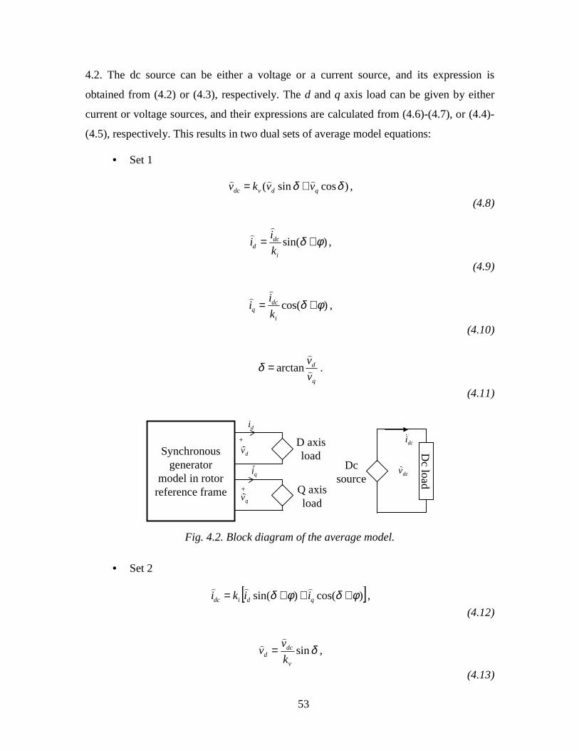
53
4.2. The dc source can be either a voltage or a current source, and its expression is
obtained from (4.2) or (4.3), respectively. The d and q axis load can be given by either
current or voltage sources, and their expressions are calculated from (4.6)-(4.7), or (4.4)-
(4.5), respectively. This results in two dual sets of average model equations:
• Set 1
)cossin( δδ qdvdc vvkv += ,
(4.8)
)sin( φδ +=i
dcd k
ii
,
(4.9)
)cos( φδ +=i
dcq k
ii
,
(4.10)
q
d
v
v
arctan=δ .
(4.11)
Synchronousgenerator
model in rotorreference frame
+
+
Dc loa
d
D axisload
Q axisload
Dcsource
vd
id
vq
iq
vdc
idc
Fig. 4.2. Block diagram of the average model.
• Set 2
[ ])cos()sin( φδφδ +++= qdidc iiki
,
(4.12)
δsinv
dcd k
vv
= ,
(4.13)

54
δcosv
dcq k
vv
= ,
(4.14)
q
d
v
v
arctan=δ .
(4.15)
It can be seen that, both in Set 1 and Set 2, an equation for calculation of rotor
angle δ was included among the average model’s equations. More generally, if the
generator’s mechanical transients were modeled, angle δ should be calculated according
to (2.17). In our case, rotor speed is set as a model parameter, and δ can change only due
to electrical transients; therefore, it can be calculated directly from the armature voltages
in the dq reference frame.
It can be seen that the average model’s equations establish a ‘transformer-like’
relationship between the generator’s output in the dq reference frame, and the rectifier’s
dc output. For example, if Set 1 is considered, dc output voltage is calculated from
armature d and q axis voltages, and the generator’s armature currents in the dq reference
frame are calculated from the dc output current. However, the presence of angle δ in (4.9)
and (4.10) causes the armature currents in the dq reference frame to be dependent also on
the armature voltages in the dq reference frame. That is a consequence of the fact that the
generator is not an ideal voltage source.
An analogous conclusion can be reached if Set 2 of the average model equations is
considered.
Set 1 of the average model equations can be written in a somewhat different form if
the equation for calculation of angle δ is incorporated into other equations. That can be
done by expanding sin(δ+φ) and cos(δ+φ), and replacing sinδ with dcdv vvk
/ , and cosδ
with dcqv vvk
/ . That results in:
• Set 1a
55
22qdvdc vvkv += ,
(4.16)
dc
dcqdd v
ivkvki
)( sincos += ,
(4.17)
dc
dcdqq v
ivkvki
)( sincos −= ,
(4.18)
where
i
v
k
kk
φcoscos = ,
(4.19)
i
v
k
kk
φsinsin = .
(4.20)
Mathematically, Set 1, Set 2 and Set 1a are completely equivalent to each other.
However, when simulation of the average model is performed, sometimes one set of
equations is more convenient than another, as far as the calculation of the steady state
operating point and convergence problems are regarded. It is useful, therefore, to use
them interchangeably in order to obtain the best simulation results.
4.3. Verification of the average model
In order to verify the average model, the simulation results obtained with it can be
compared to the simulation results obtained with the switching model, and to
measurement results. Between these two choices, comparison with the switching model
results are more meaningful for verification of the average model, because they are not
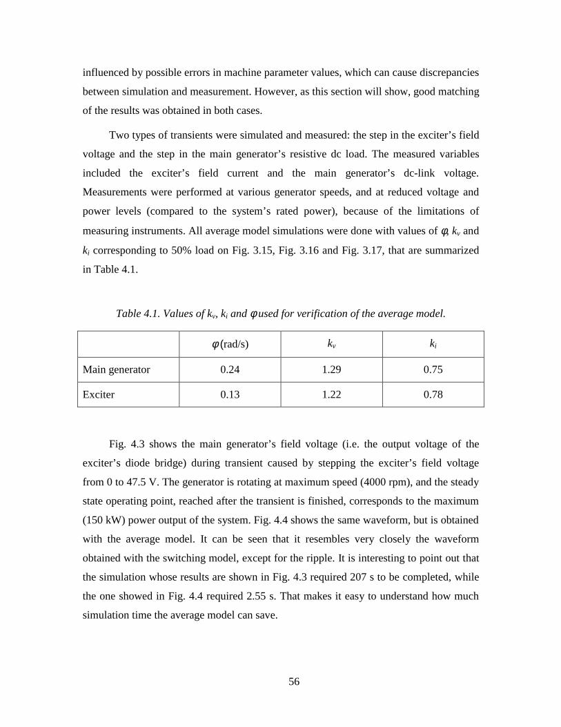
56
influenced by possible errors in machine parameter values, which can cause discrepancies
between simulation and measurement. However, as this section will show, good matching
of the results was obtained in both cases.
Two types of transients were simulated and measured: the step in the exciter’s field
voltage and the step in the main generator’s resistive dc load. The measured variables
included the exciter’s field current and the main generator’s dc-link voltage.
Measurements were performed at various generator speeds, and at reduced voltage and
power levels (compared to the system’s rated power), because of the limitations of
measuring instruments. All average model simulations were done with values of φ, kv and
ki corresponding to 50% load on Fig. 3.15, Fig. 3.16 and Fig. 3.17, that are summarized
in Table 4.1.
Table 4.1. Values of kv, ki and φ used for verification of the average model.
φ (rad/s) kv ki
Main generator 0.24 1.29 0.75
Exciter 0.13 1.22 0.78
Fig. 4.3 shows the main generator’s field voltage (i.e. the output voltage of the
exciter’s diode bridge) during transient caused by stepping the exciter’s field voltage
from 0 to 47.5 V. The generator is rotating at maximum speed (4000 rpm), and the steady
state operating point, reached after the transient is finished, corresponds to the maximum
(150 kW) power output of the system. Fig. 4.4 shows the same waveform, but is obtained
with the average model. It can be seen that it resembles very closely the waveform
obtained with the switching model, except for the ripple. It is interesting to point out that
the simulation whose results are shown in Fig. 4.3 required 207 s to be completed, while
the one showed in Fig. 4.4 required 2.55 s. That makes it easy to understand how much
simulation time the average model can save.

57
0
50
100
150
200
250
0 0.05 0.1 0.15 0.2 0.25 0.3 0.35 0.4
Time (s)
Mai
n ge
nera
tor's
fiel
d vo
ltage
(V
)
Fig. 4.3. Switching model simulation: the main generator’s field voltage at the exciter’sfield voltage step from 0 V to 47.5 V (n=4000 rpm, Rl=4.27 Ω).
0
50
100
150
200
250
0 0.05 0.1 0.15 0.2 0.25 0.3 0.35 0.4
Time (s)
Mai
n ge
nera
tor's
fiel
d vo
ltage
(V
)
Fig. 4.4. Average model simulation: the main generator’s field voltage at the exciter’sfield voltage step from 0 V to 47.5 V (n=4000 rpm, Rl=4.27 Ω).
Fig. 4.5 shows the measured waveforms of the exciter’s field current and main dc-
link voltage during transient caused by a 0 to 8.5 V step in the exciter’s field voltage. The
generator is rotating at 3050 rpm, and the load resistance is 18.75 Ω, which corresponds
to a steady state power output of approximately 12 kW. Fig. 4.6 shows the same

58
waveforms obtained with the switching model simulation, and Fig. 4.7 shows average
model simulation results. Even though the waveforms in Fig. 4.5, Fig. 4.6 and Fig. 4.7
are very similar, there are some differences among them that require a comment. First,
the measurement shows some dc-link voltage even at zero exciter’s field voltage. That is
due to remnant magnetism in the real machine, which is not taken into account by the
generator model. Second, when the switching model simulation was done, the exciter’s
field voltage needed to be lower (7 V), compared to the measured case (8.5 V), in order
to achieve the same steady state dc-link voltage. That can be attributed to errors in the
exciter’s and main generator’s parameters. Third, the value of steady state dc-link voltage
obtained with the average model is slightly lower than the value obtained with the
switching model. That can be attributed to the fact that, when the average model
simulation was done, values of φ, kv and ki corresponding to 50% load in Fig. 3.15, Fig.
3.16 and Fig. 3.17 were chosen, even though actual output power was less than 10% of
rated power. The speed, also, was not such that it would correspond to the power
according to Fig. 3.14.
Exciter’s field current (0.2 A/div)
Dc link voltage (100 V/div)
0 A
0 V
Fig. 4.5. Measurement: dc-link voltage and the exciter’s field current at the exciter’s fieldvoltage step from 0 V to 8.5 V (n=3050 rpm, Rl=18.75 Ω).

59
-200
-100
0
100
200
300
400
500
600
0 0.2 0.4 0.6 0.8 1 1.2 1.4 1.6 1.8 2
Time (s)
-0.2
0
0.2
0.4
0.6
0.8
1
1.2
1.4
Dc link voltage Exciter's field current
Fig. 4.6. Switching model simulation: dc-link voltage and the exciter’s field current at theexciter’s field voltage step from 0 V to 7 V (n=3050 rpm, Rl=18.75 Ω).
-200
-100
0
100
200
300
400
500
600
0 0.2 0.4 0.6 0.8 1 1.2 1.4 1.6 1.8 2
Time (s)
-0.2
0
0.2
0.4
0.6
0.8
1
1.2
1.4
Dc link voltage Exciter's field current
Fig. 4.7. Average model simulation: dc-link voltage and the exciter’s field current at theexciter’s field voltage step from 0 V to 7 V (n=3050 rpm, Rl=18.75 Ω).
Measured and simulated waveforms during transient caused by interruption of the
exciter field current are shown in Fig. 4.8, Fig. 4.9 and Fig. 4.10. Regarding the small
differences in waveforms, the same comments can be applied as in the previous case.

60
0V
0A
Dc link voltage (100 V/div)
Exciter’s field current (0.2 A/div)
Fig. 4.8. Measurement: dc-link voltage and the exciter’s field current at the exciter’s fieldcurrent step from 0.34 A to 0 A (n=3050 rpm, Rl=18.75 Ω.).
-200
-100
0
100
200
300
400
500
600
2 2.2 2.4 2.6 2.8 3 3.2 3.4 3.6 3.8 4
Time (s)
-0.2
0
0.2
0.4
0.6
0.8
1
1.2
1.4
Dc link voltage Exciter's field current
Fig. 4.9. Switching model simulation: dc-link voltage and the exciter’s field current at theexciter’s field current step from 0.38 A to 0 A (n=3050 rpm, Rl=18.75 Ω).

61
-200
-100
0
100
200
300
400
500
600
0 0.2 0.4 0.6 0.8 1 1.2 1.4 1.6 1.8 2
Time (s)
-0.2
0
0.2
0.4
0.6
0.8
1
1.2
1.4
Dc link voltage Exciter's field current
Fig. 4.10. Average model simulation: dc-link voltage and the exciter’s field current at theexciter’s field current step from 0.38 A to 0 A (n=3050 rpm, Rl=18.75 Ω).
The transient caused by stepping the main generator’s resistive dc load is shown in
Fig. 4.11, Fig. 4.12 and Fig. 4.13 (measurement, switching model simulation and average
model simulation, respectively). A slight undershoot, not registered during the
measurement, can be noticed in the simulated waveform of the dc-link voltage; it can be
attributed to errors in machine parameters. Also, for the same reason as before, the steady
state dc-link voltage is somewhat larger when obtained with the average model than with
the switching model.
It is also interesting to notice the effect of the large generator’s synchronous
reactance on Fig. 4.11: when load resistance drops by a factor of two, the output voltage
drops by a large amount (approximately a factor of two in this case). The same effect can
be observed in Fig. 4.14 and Fig. 4.15, which show dc-link voltage during the transient
due to the disconnection of 19 Ω (2 kW) resistive dc load, at two different speeds (2000
rpm and 3700 rpm). It can be seen how the difference in dc-link voltage before and after
the transient depends on generator speed (i.e. the generator’s synchronous reactance).

62
Exciter’s field current (0.2 A/div)
Dc link voltage (100 V/div)
0 V
0 A
Fig. 4.11. Measurement: dc-link voltage and the exciter’s field current at resistive loadstep from 12.5 Ω to 6.25 Ω (n=3100 rpm, vfd=11.6 V).
0
100
200
300
400
500
600
700
800
1.5 1.6 1.7 1.8 1.9 2 2.1 2.2 2.3 2.4 2.5
Time (s)
-1
-0.8
-0.6
-0.4
-0.2
0
0.2
0.4
0.6
Dc link voltage Exciter's field current
Fig. 4.12. Switching model simulation: dc-link voltage and the exciter’s field current atresistive load step from 12.5 Ω to 6.25 Ω (n=3100 rpm, vfd=11.6 V).

63
0
100
200
300
400
500
600
700
800
1.5 1.6 1.7 1.8 1.9 2 2.1 2.2 2.3 2.4 2.5
Time (s)
Dc
link
volta
ge (
V)
-1
-0.8
-0.6
-0.4
-0.2
0
0.2
0.4
0.6
Exciter field current (A
)
Dc link voltage Exciter field current
Fig. 4.13. Average model simulation: dc-link voltage and the exciter’s field current atresistive load step from 12.5 Ω to 6.25 Ω (n=3100 rpm, vfd=11.6 V).
(b)
-50
0
50
100
150
20 0
250
30 0
350
0 1 2 3 4 5 6 7 8 9 10Time (s)
Dc link voltage
1 s/div, 50 V/div0V
(a)
Fig. 4.14. (a) measurement, (b) average model simulation: dc-link voltage in transientfollowing disconnection of 19 Ω resistive dc load (n=2000 rpm, vfd=3.4 V in (a), vfd=1.85
V in (b)).

64
-100
0
100
20 0
30 0
40 0
500
60 0
700
0 1 2 3 4 5 6 7 8 9 10Time (s)
Dc link voltage0V
(b)(a)
1 s/div, 100 V/div
Fig. 4.15. (a) measurement, (b) average model simulation: dc-link voltage in transientfollowing disconnection of 19 Ω resistive dc load (n=3700 rpm, vfd=2.8 V in (a), vfd=2.03
V in (b)).
The results presented in this section lead to the following conclusions:
1. Transient waveforms obtained with average model match extremely well, in the
moving average sense, transient waveforms obtained with the switching model.
Slight discrepancies (about 5%) in steady state values can be attributed to the
fact that the same values of φ, kv and kI, relative to 50% load in Fig. 3.15, Fig.
3.16 and Fig. 3.17, were used for all average model simulation, regardless of
the operating point. Differences in dynamic waveforms characteristics
(overshoot, undershoot, settling time) are practically invisible between the
switching and average model results.
2. All simulation results (switching and average model) match reasonably well
with measurement results. The differences can be explained by either the
generator model’s inherent drawbacks (absence of modeling of magnetic
saturation and remnant magnetism), or by errors in the main generator’s and
exciter’s parameters.
3. Based on the above conclusions, the average model presented in Section 4.2.2
can be used in order to predict dynamic behavior of the system shown in Fig.
3.2. Validity of the model will be discussed more generally in the following
section.
65
4.4. Validity of the average model
4.4.1. Discussion of first harmonic assumption
Based on the discussion regarding the importance of higher harmonics for
operation of a diode bridge loaded synchronous generator (Section 3.3), the following
conditions must be satisfied so that the average model represents the actual system’s
behavior with sufficient accuracy:
1. The generator’s harmonics other than fundamental deliver negligible active
power;
2. The diode rectifier output is well filtered (large L, or C, or both).
In most practical applications, both of these conditions will be true. Almost any
synchronous machine (or, more generally, any non-ideal electrical source) will have the
reactive part of its internal impedance dominant when compared to the resistive part. That
will cause the active power associated with higher harmonics at the rectifier’s input to be
negligible. Similarly, there is always some kind of filter at the output of the diode bridge.
Because of that, either dc voltage or dc current at the rectifier’s output will have a
negligible ripple.
Therefore, it can be expected that the above requirements will not limit the
possibility of practical applications of the developed average model.
4.4.2. Average model and diode rectifier losses
It was explained in Section 3.3 how the diode’s forward voltage drop influences
calculation of the exciter’s kv at light load. It is the purpose of this section to discuss, in a

66
somewhat more detailed manner, how diode rectifier losses can be related to parameters
of the average model.
It needs to be made clear, at the very beginning of this discussion, that all switching
model simulation results presented in previous sections of this work were obtained with
the default diode model available in PSpice. That model accounts for forward voltage
drop, i.e. diodes used in switching model simulations were characterized by a forward
voltage drop larger than zero. However, no attempts were made to accurately model real
diodes used in the actual generator set that is the object of this study. Therefore, all
results regarding relationships between diode losses and average model parameters need
to be interpreted from only the conceptual point of view, without attributing to them any
practical meaning relative to the actual studied system.
The average model’s parameters (φ, kv and ki) were obtained based on switching
model simulations. Therefore, the average model contains information about diode
forward voltage drop and losses. That can be quantified if the diode rectifier input power
is expressed as
qqddin ivivp += .
(4.21)
When d and q axis voltages are substituted according to (4.13) and (4.14), and
currents according to (4.9) and (4.10), input power can be written as
dcdciv
in ivkk
p φcos= .
(4.22)
The product of dc voltage and current in (4.22) can be recognized as output power
of the diode rectifier
dcdcout ivp = .
(4.23)
Therefore, efficiency of the diode rectifier can be expressed as

67
φη
cosiv
in
out kk
p
p ==
.
(4.24)
This last expression relates efficiency of the diode rectifier directly to the
parameters of the generator/rectifier average model. Fig. 4.16 shows variation of the
exciter’s and the main generator’s rectifier efficiency with load, when speed versus load
relationship is the one shown in Fig. 3.14. The main generator’s rectified output dc
voltage is kept at 800 V at any operating point, which makes the main generator’s diode
rectifier’s output power proportional to the output current. At the same time, diode losses
are approximately proportional to the diode current. Consequently, the main generator’s
rectifier efficiency does not change with load variations.
0.85
0.86
0.87
0.88
0.89
0.9
0.91
0.92
0.93
0.94
0.95
0.96
0.97
0.98
0.99
1
0 10 20 30 40 50 60 70 80 90 100Load %
Effi
cien
cy
Exciter's rectifier
Main generator's rectifier
Fig. 4.16. Diode rectifier’s efficiency variation with load.
The exciter’s case is different. The exciter’s rectifier needs to provide variable dc
voltage for the main generator’s field winding. At low output power, this voltage is low
enough to decrease significantly the exciter’s diode rectifier’s efficiency.
Fig. 4.16 also allows for discussion, from a power balance point of view, the
legitimacy of the use of φ, kv and ki values relative to 50% load for any operating point.
(They were used in Section 4.3, when the average model was verified through
comparison with switching model simulation and measurements.) It can be seen that, for

68
the main generator, rectifier efficiency at 50% load is practically equal to efficiency at
any other load; therefore, use of φ, kv and ki relative to 50% load does not introduce any
error, as far as power balance is concerned. For the exciter, however, efficiency at 50%
load is considerably different from efficiency at a lower or higher load. However, power
processed by the exciter is very small compared to the power processed by the main
generator. Consequently, it can be said that error introduced by the use of ‘wrong’ values
of exciter’s φ, kv and ki does not affect significantly the power balance of the whole
system.
The ideal case, (lossless diodes and no reactive components on either side of diode
rectifier) is characterized by η=1, φ=0, π/23=vk , )23/(π=ik , i.e.
vi k
k1= ,
(4.25)
which recalls the relationship characterizing an ideal transformer.
If the diode rectifier is lossless (η=1), but reactive components are present at both
sides of diode rectifier (φ>0), (4.24) yields
φcos=ivkk .
(4.26)
In this case, product kvki can be interpreted as describing the reactive nature of source and
load impedances. When losses in the diode rectifier are negligible (1≈η ), such as in the
main generator’s case, expression (4.26) can be considered alternative to (3.1) for
calculation of φ, once kv and ki are calculated.
The real case (η<1, φ>0) is described by
ηφcos=ivkk ,
(4.27)
which means that product kvki reflects both the reactive nature of source and load
impedances, and losses in the system.

69
4.4.3. Use of the average model with different loads and sources
The average model’s equations were developed based on the switching model
results obtained with resistive load at the main generator’s dc-link. Consequently, the
validity of the average model can be questioned if a different dc load (e.g., an inverter) is
applied, as in the practical system shown in Fig. 1.1. In order to justify the use of the
average model with such a dc load, it needs to be remembered that the average model’s
parameters (φ, kv and ki) were obtained from the switching model steady state waveforms.
If the dc-link capacitor is large enough to provide the high-frequency current component
required by the inverter, there is no reason why the generator’s voltage and current steady
state waveforms should be different with the inverter dc load, as opposed to the resistive
dc load. Essentially, the main generator still has a dc voltage source connected to its
rectifier’s output, and the average model can still be considered valid.
The above justification of the use of the average model does not mean, however,
that the actual inverter can be approximated by a resistor. An inverter operating in closed
loop is a constant power load in the sense that, if the dc-link voltage rises for any reason,
the closed loop inverter will decrease its duty cycle, which will result in smaller current
being drawn from the dc-link. That, small-signal-wise, can be represented by a negative
resistor [22] or, less accurately but easier to apply to control design, a current source. A
dc current source connected to the dc-link provides the desired steady state operating
point, but does not introduce any damping at the output (damping does not exist with the
actual closed-loop inverter, but it would be introduced if the inverter were represented by
a resistor). Therefore, it can be expected that it will be more difficult to stabilize the
closed loop system with current source load than with resistive load.
The average model was developed for the case in which an independent
synchronous generator feeds a diode rectifier. However, it can be generalized to any case
in which a diode rectifier is fed by a three-phase voltage source with complex source
impedance; it suffices to write equations of the particular voltage source of interest, and
transform them to the dq reference frame. The average model is then directly applicable.

70
The model’s strength, however, consists in taking into account the effects of the non-
ideal operation of the diode rectifier. Therefore, the use of the model is meaningful
primarily in cases in which the source’s impedance causes the rectifier’s strongly non-
ideal operation.
4.5. Linearized average model
4.5.1. Linearization of model equations
The average model’s equations, presented in Section 4.2.2, are non-linear because
they contain products of variables, as well as trigonometric functions. For some purposes,
such as control-loop design, it is necessary to study the linearized system. In many cases,
software used for simulation of the average model is capable of linearizing system
equations, after it determines the steady-state operating point. However, it is useful to
find analytically the linearized version of average model equations. That makes it
possible to easily simulate cases that would cause numerical problems in determining the
steady state operating point, as well as to find the linearized state space representation of
the system.
In this section, linearized versions of (4.8)-(4.11) (Set 1) and (4.16)-(4.18) (Set 1a)
of average model equations will be presented. Linearizing an equation around a certain
steady state operating point is equivalent to finding Taylor’s expansion of the function
represented by that equation, and neglecting all terms other than the constant and the
linear term. The obtained linear expression is valid only for small perturbations around
the selected operating point.
In this and the following sections, the steady state value of an average variable x
will be denoted as X, while x~ will stand for small perturbation of the same variable. With
these conventions, the following linearized version of (4.8)-(4.11) can be obtained:

71
δ~~~~321 kvkvkv qddc ++= ,
(4.28)
δ~~~54 kiki dcd += ,
(4.29)
δ~~~76 kiki dcq += ,
(4.30)
qd vkvk ~~~98 +=δ ,
(4.31)
where
k kv1 = sin∆ ,(4.32)
k kv2 = cos∆ ,(4.33)
)sincos(3 ∆−∆= qdv VVkk ,
(4.34)
kki
4 =+sin( )∆ ϕ
,
(4.35)
kI
kdc
i5 =
+cos( )∆ ϕ,
(4.36)
kki
6 =+cos( )∆ ϕ
,
(4.37)
kI
kdc
i7 = −
+sin( )∆ ϕ,
(4.38)
72
∆+∆∆=
sincos
cos8
dq VVk ,
(4.39)
∆+∆∆−=
sincos
sin9
dq VVk .
(4.40)
Linearization of (4.16)-(4.18) yields
qddc vcvcv ~~~21 += ,
(4.41)
qddcdcd vcvcvcici ~~~~~6543 +++= ,
(4.42)
qddcdcq vcvcvcici ~~~~~10987 +++= ,
(4.43)
where
221
qd
dv
VV
Vkc
+= ,
(4.44)
222
qd
qv
VV
Vkc
+= ,
(4.45)
dc
qd
V
VkVkc sincos
3
+= ,
(4.46)
dc
d
V
Ic −=4 ,
(4.47)

73
dc
dc
V
Ikc cos
5 = ,
(4.48)
dc
dc
V
Ikc sin
6 = ,
(4.49)
dc
dq
V
VkVkc sincos
7
−= ,
(4.50)
dc
q
V
Ic −=8 ,
(4.51)
dc
dc
V
Ikc sin
9 −= ,
(4.52)
dc
dc
V
Ikc cos
10 = ,
(4.53)
4.5.2. Linearized state-space representation
The purpose of this section is to find a linear state space representation of the
system consisting of the exciter, main generator and a dc load. This is obtained by
combining the machine’s equations (2.6)-(2.12) with the linearized generator/rectifier
average model’s equations, and an equation describing the dc load. This is an
algebraically tedious process that does not introduce any new concepts. Some readers,
therefore, may wish not to pay particular attention to sections 4.5.2.1 and 4.5.2.2, in
which algebraic manipulations are carried out, but to use results given in section 4.5.2.3.

74
If the generator’s speed is constant and treated as a parameter of the system, (2.6)-
(2.12) are linear differential equations, and they can be rewritten for small perturbations
by simply adding a tilde to all currents and voltages. Since both the exciter’s and the
main generator’s equations will be treated in this section, index ‘e’ will be added to all
parameters and variables relative to the exciter, and index ‘a’ to all those relative to the
main generator, in order to be able to distinguish between them. For example, Ras will
stand for the armature resistance of the main generator, ied will stand for exciter’s d axis
armature current, and so on.
4.5.2.1. Exciter’s equations
With the above conventions, the exciter’s equations can be written as
dt
idL
dt
idLLiLLiRv efd
emded
emdelseqemqelseedesed
~~)(
~)(
~~ ++−++−= ω ,
(4.54)
dt
idLLiLiLLiRv eq
emqelsefdemdeedemdelseeqeseq
~)(
~~)(
~~ +−++−−= ωω ,
(4.55)
dt
idLL
dt
idLiRv efd
emdelfded
emdefdefdefd
~)(
~~~ ++−= .
(4.56)
These equations obviously suggest use of the exciter’s currents for state variables.
In equation (4.56), efdv~ is considered to be the input to the system, which means that
(4.56) is already in a form suitable for obtaining linear state space representation. What
remains to be done is to express edv~ and eqv~ as linear functions of currents and their
derivatives, and to substitute the found expressions in (4.54) and (4.55). That can be
achieved by combining linearized equations of the generator/rectifier average model

75
(4.28)-(4.31) with the exciter’s dc load equation. By substituting (4.31) into (4.28), (4.29)
and (4.30), we get
eqededc vkvkv ~~~239138 += ,
(4.57)
eqededced vkkvkkiki ~~~~95854 ++= ,
(4.58)
eqededceq vkkvkkiki ~~~~97876 ++= ,
(4.59)
where
831138 kkkk += ,
(4.60)
932239 kkkk += .
(4.61)
The exciter’s dc load is represented by the main generator’s field winding, whose
equation is
dt
idL
dt
idLL
dt
idLiRv akd
amdafd
amdalfdad
amdafdafdafd
~~)(
~~~ +++−= .
(4.62)
The main generator’s field voltage in (4.62) is referred to the armature, but it is
related to the exciter’s rectified output voltage by means of the main generator’s field-to-
armature turns ratio ta as
edcaafd vtv ~~ = .
(4.63)
Similarly, for currents
edca
afd it
i~1~ = .
(4.64)
76
When (4.62), (4.63) and (4.64) are combined, the following exciter’s load equation
is obtained:
dt
id
t
L
dt
id
t
LL
dt
id
t
Li
t
Rv akd
a
amdedc
a
amdalfdad
a
amdedc
a
afdedc
~~~~~
22 ++
+−= .
(4.65)
It can be seen that (4.65) contains main generator’s d axis currents; that accounts
for dynamic coupling between the exciter and the main generator.
Now it is possible to find expressions for edv~ and eqv~ by eliminating edcv~ and edci~
from the system of equations consisting of (4.57)-(4.59) and (4.65). That yields
dt
idlk
dt
idlk
dt
idlir
dt
idlirv akd
aead
aeeq
edqeqedqed
eddededded
~~~~
~~~
99 +−+++= ,
(4.66)
dt
idlk
dt
idlk
dt
idlir
dt
idlirv akd
aead
aeeq
eqqeqeqqed
eqdedeqdeq
~~~~
~~~
88 −++++= ,
(4.67)
where
)()( 13892398652398138974det kkkkkkkkkkkkk −+−=(4.68)
det
2972396
k
t
Rkkkk
r a
afd
edd
+= ,
(4.69)
det
2952394
k
t
Rkkkk
r a
afd
edq
+−= ,
(4.70)
det2
97 )(
kt
LLkkl
a
amdalfdedd
+= ,
(4.71)

77
det2
95 )(
kt
LLkkl
a
amdalfdedq
+−= ,
(4.72)
det
2871386
k
t
Rkkkk
r a
afd
eqd
+−= ,
(4.73)
det
2851384
k
t
Rkkkk
r a
afd
eqq
+−= ,
(4.74)
det2
87 )(
kt
LLkkl
a
amdalfdeqd
+−= ,
(4.75)
det2
85 )(
kt
LLkkl
a
amdalfdeqq
+= ,
(4.76)
amda
ae Lkt
kkkkl
det
6574 −= ,
(4.77)
The same process allows us to find the following expression for the main
generator’s field current:
eqaeqedaedafd ihihi~~~ += ,
(4.78)
where
det
8723997138
kt
kkkkkkh
aaed
−= ,
(4.79)

78
det
9513885239
kt
kkkkkkh
aaeq
−= .
(4.80)
Expressions (4.66) and (4.67) will be substituted into (4.54) and (4.55),
respectively, in order to obtain linear state space representation. Expression (4.78) allows
us to replace the main generator’s field current by a linear combination of the exciter’s
armature currents; that eliminates the main generator’s field current as a state variable,
and reduces the order of the system by one.
4.5.2.2. Main generator’s equations
It is possible to proceed now with rewriting the main generator’s equations for
small perturbations. In doing so, the field winding equation is omitted, since it has
already been used as the exciter’s load equation, and the main generator’s field current is
substituted according to (4.78). That yields
,)(
)()(
dt
diL
dt
ihihdL
dt
diLLiLiLLiRv
akdamd
eqaeqedaedamd
adamdalsakqamqaaqamqalsaadasad
++
+
++−−++−= ωω
(4.81)
,)(
)()(
dt
diL
dt
diLLiL
ihihLiLLiRv
akqamq
aqamqalsakdamda
eqaeqedaedamdaadamdalsaaqasaq
++−+
++++−−=
ω
ωω
(4.82)
dt
diLL
dt
ihihdL
dt
diLiR akd
amdalkdeqaeqedaed
amdad
amdakdakd )()(
0 +++
+−= ,
(4.83)

79
dt
diLL
dt
diLiR akq
amqalkqaq
amqakqakq )(0 ++−= .
(4.84)
It can be seen that (4.83) and (4.84) are already in a convenient form for state space
representation. As in the exciter’s case, it is necessary to find expressions which will
linearly relate adv~ and aqv~ to state variables and their derivatives. Again, that can be done
by combining linearized equations of generator/rectifier average model (this time, (4.41)-
(4.43) will be used) with the main generator’s load equation.
It can be assumed at this point, and in accordance with the discussion in Section
4.4.3, that the main generator’s load is represented by a current source loadi~
. In that case,
the main generator’s load equation is given by
~~
~i Cdv
dtiadc
adcload= + .
(4.85)
If the above expression is used to eliminate adci~
from (4.42) and (4.43), the
following expressions are obtained for adv~ and aqv~ :
loadadladc
addcadcaddcaqadqadaddad irdt
vdcvhirirv
~~~~~~ ++++= ,
(4.86)
loadaqladc
aqdcadcaqdcaqaqqadaqdaq irdt
vdcvhirirv
~~~~~~ ++++= ,
(4.87)
where
96105det
1
ccccc
−= ,
(4.88)
10detccradd = ,
(4.89)
80
6detccradq −= ,
(4.90)
)( 10486det ccccchaddc −= ,
(4.91)
Cccccccaddc )( 10376det −= ,
(4.92)
)( 10376det cccccradl −= ,
(4.93)
9detccraqd −= ,
(4.94)
5detccraqq = ,
(4.95)
)( 8594det ccccchaqdc −= ,
(4.96)
Cccccccaqdc )( 7593det −= ,
(4.97)
)( 7593det cccccraql −= .
(4.98)
In (4.86) and (4.87), loadi~
needs to be treated as input to the system. These
expressions will be used to substitute for armature voltages in (4.81) and (4.82),
respectively.
4.5.2.3. State-space representation of the system
State-space representation of the system needs to have the following form:
81
x Ax Bu= + ,(4.99)
where
=
adc
akq
akd
aq
ad
efd
eq
ed
v
i
i
i
i
i
i
i
~
~
~
~
~
~
~
~
x
(4.100)
is the vector of state variables, and
u =
~~v
iefd
load
(4.101)
is the vector of system’s inputs.
In order to find matrices A and B from (4.99), the system’s equations will be
written in the form
Ex Fx Gu = + .(4.102)
After that, matrices A and B can be calculated as
A E F= −1 ,(4.103)
B E G= −1 .(4.104)
In order to obtain the form given by (4.102), for each state variable, an equation is
written in the following way:

82
• For the exciter’s armature d axis current, by combining (4.54) and (4.66);
• For the exciter’s armature q axis current, by combining (4.55) and (4.67);
• For the exciter’s field current, by using (4.56);
• For the main generator’s armature d axis current, by combining (4.81) and
(4.86);
• For the main generator’s armature q axis current, by combining (4.82) and
(4.87);
• For the main generator’s d axis damper winding current, by using (4.83);
• For the main generator’s q axis damper winding current, by using (4.84);
• For dc-link voltage, by combining (4.41) with (4.86) and (4.87).
When these eight equations are written in matrix form, the following matrices E, F
and G are gotten:
)(
0000000
000000
0000
0)(0000
00)(0
000000
0000)(
000)(
2188
88
88
99
aqdcaddc
amqalkqamq
amdalkdamdaeqamdaedamd
aqdcamqamqals
addcamdamdalsaeqamdaedamd
emdelfdemd
aeaeeqqemqelseqd
aeaeemdedqeddemdels
cccce
e
LLL
LLLhLhL
cLLL
cLLLhLhL
LLL
lklklLLl
lklkLllLL
+−=
+−+−
−+−−+−
+−−++−−
−−++−
=E
(4.105)
1
00000
0000000
0000000
0)(0
0)(000
0000000
00000)(
000000)(
2188
2185
2184
888584
−+=
+=
+=
−−
−+++−−+−+
−−+++
+−+
=
aqdcaddc
aqqadq
aqdadd
akq
akd
aqdcamdaaqqasamdalsaaqdaeqamdaaedamda
addcamqaamqalsaadqaddas
efd
emdeeqqesemdelseeqd
emqelseedqeddes
hchcf
rcrcf
rcrcf
fff
R
R
hLrRLLrhLhL
hLLLrrR
R
LrRLLr
LLrrR
ωωωωωω
ωωω
F
(4.106)

83
+
=
aqladl
aql
adl
rcrc
r
r
210
00
00
0
0
01
00
00
G.
(4.107)
If a resistive load were connected to the dc-link, equations which allow us to determine
matrices E, F and G can easily be modified by substituting
l
dcload R
vi
~~ =
(4.108)
where Rl is the load resistance. In that case, the only input to the system is represented by
exciter’s field voltage.
If dc-link voltage is considered to be system’s output, the output equation can be
written in the form
DuCx +=adcv~ ,
(4.109)
where
[ ]10000000=C ,(4.110)
[ ]0=D .(4.111)
4.5.3. Transfer functions
A linearized representation of the system allows to find system’s transfer functions.
For dc-link voltage controller design, it is necessary to have Bode plots of efdadc vv ~/~ (also

84
referred to as control-to-output) transfer function. This transfer function can be found
from linearized state space representation as
DBAIC +−= −1)(~
~s
v
v
efd
adc .
(4.112)
However, it is almost always faster to plot this transfer function by directly
performing frequency-domain simulation of the system’s average model. Fig. 4.17 and
Fig. 4.18 show thus obtained Bode plots of magnitude and phase of efdadc vv ~/~ at two
different operating points. In both cases, dc load is represented by a current source.
-150
-100
-50
0
50
100
0.01 0.1 1 10 100 1000Frequency (Hz)
3340 rpm, 105 kW
2020 rpm, 15 kW
Fig. 4.17. Magnitude of the exciter’s field voltage-to-dc-link voltage transfer functionwith current source load, at two different operating points.

85
-400
-350
-300
-250
-200
-150
-100
-50
0
0.01 0.1 1 10 100 1000Frequency (Hz)
Pha
se (
dB)
2020 rpm, 15 kW
3340 rpm, 105 kW
Fig. 4.18. Phase of the exciter’s field voltage-to-dc-link voltage transfer function withcurrent source load, at two different operating points.
It can be seen from these figures that this system can hardly be approximated with a
first-, or even second-order transfer function. The phase, for example, reaches values well
below –180º (which would be the minimum phase reached by a second-order transfer
function). These facts become even more obvious if the transfer function’s poles and
zeros are found numerically (from numerator and denominator of (4.112)). They are
listed in Table 4.2 for the operating point characterized by 3340 rpm and 105 kW current
source load. It will be seen in the following chapter that all frequencies below 100 Hz are
of interest for dc-link voltage control-loop design. It is clear from Table 4.2 that there are
six poles and three zeros in that frequency range. Therefore, accurate Bode plots of this
transfer function, obtainable with the use of the generator/rectifier average model, are
essential for dc-link voltage control design.
Fig. 4.17 and Fig. 4.18 show that both magnitude and phase of control-to-output
transfer function change as operating point changes. Since the load is represented by a
current source, which does not contribute to damping of the system, this dependence can
be attributed mainly to changes in generator speed, i.e. to the fact that the generator’s
reactances increase proportionally to the speed. The question then arises, which operating
point to select as the basis for control-loop design. It can be argued that, at higher speed
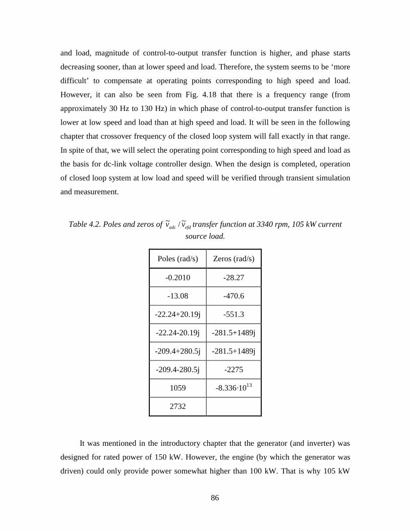
86
and load, magnitude of control-to-output transfer function is higher, and phase starts
decreasing sooner, than at lower speed and load. Therefore, the system seems to be ‘more
difficult’ to compensate at operating points corresponding to high speed and load.
However, it can also be seen from Fig. 4.18 that there is a frequency range (from
approximately 30 Hz to 130 Hz) in which phase of control-to-output transfer function is
lower at low speed and load than at high speed and load. It will be seen in the following
chapter that crossover frequency of the closed loop system will fall exactly in that range.
In spite of that, we will select the operating point corresponding to high speed and load as
the basis for dc-link voltage controller design. When the design is completed, operation
of closed loop system at low load and speed will be verified through transient simulation
and measurement.
Table 4.2. Poles and zeros of efdadc vv ~/~ transfer function at 3340 rpm, 105 kW current
source load.
Poles (rad/s) Zeros (rad/s)
-0.2010 -28.27
-13.08 -470.6
-22.24+20.19j -551.3
-22.24-20.19j -281.5+1489j
-209.4+280.5j -281.5+1489j
-209.4-280.5j -2275
1059 -8.336·1013
2732
It was mentioned in the introductory chapter that the generator (and inverter) was
designed for rated power of 150 kW. However, the engine (by which the generator was
driven) could only provide power somewhat higher than 100 kW. That is why 105 kW

87
were selected as the maximum power of the system for control design purpose. The
corresponding speed was assumed to be 3340 rpm.
It was argued in Section 4.4.3 that current source load, as opposed to resistive load,
makes the system more difficult to stabilize in closed loop. Since the average model
allows us to find transfer functions with any kind of load, it is now possible to verify the
validity of that argument. For the sake of comparison, Fig. 4.19 and Fig. 4.20 show
magnitude and phase, respectively, of control-to-output transfer function at 3340 rpm,
105 kW, with current source load and resistive load. Table 4.3 lists poles and zeros of
control-to-output transfer function with resistive load. It can be seen that, with resistive
load, the lowest-frequency poles of the transfer function are at approximately two Hz, as
opposed to 0.03 Hz with current source load (Table 4.2). That makes the phase of
control-to-output transfer function with resistive load start decreasing at frequencies
higher than with the current source load. Also, the dc gain of the transfer function is
significantly lower with a resistive load. That is easily explained if it is remembered that,
with resistive load, an increase in the exciter’s field voltage by an amount x results in an
increase, by an amount y, in main generator’s armature voltage. Since the dc load is
resistive, the main generator’s armature current will also increase (by an amount
approximately equal to y/Rl), increasing the voltage drop at the main generator’s
synchronous reactance. With current source load, however, the main generator’s armature
current is kept constant. Therefore, an increase by x in the exciter’s field voltage will not
result in an increased voltage drop at the main generator’s synchronous reactance;
consequently, the main generator’s armature voltage will rise by an amount larger than y.
This is seen as a larger magnitude of control-to-output transfer function.
Because of the two above listed reasons (higher dc gain and poles at lower
frequencies), current source load definitely makes the system more difficult to stabilize in
closed loop at frequencies up to approximately three Hz. After that frequency, there is
almost no difference between transfer functions with current source or resistive load (that
can also be seen by comparing poles and zeros in Table 4.2 and Table 4.3), and both are
equally difficult, or easy, to compensate.

88
-150
-100
-50
0
50
100
0.01 0.1 1 10 100 1000Frequency (Hz)
Mag
nitu
de (
dB)
Current source load
Resistive load
Fig. 4.19. Magnitude of the exciter’s field voltage-to-dc-link voltage transfer function at3340 rpm, 105 kW, with different kinds of load.
-350
-300
-250
-200
-150
-100
-50
0
0.01 0.1 1 10 100 1000Frequency (Hz)
Resistive load
Current source load
Fig. 4.20. Phase of the exciter’s field voltage-to-dc-link voltage transfer function at 3340rpm, 105 kW, with different kinds of load.
Current source load, as opposed to resistive load, can therefore be adopted as a
more conservative option from a closed loop control design point of view. Consequently,
transfer function relative to a speed of 3340 rpm and a current source load of 105 kW will
represent a starting point for dc-link controller design, which is the matter of discussion
of the following chapter.

89
Table 4.3. Poles and zeros of efdadc vv ~/~ transfer function at 3340 rpm, 105 kW resistive
load.
Poles (rad/s) Zeros (rad/s)
-8.906+10.25j -30.83
-8.906-10.25j -500
-23.53+21.44j -802.3
-23.53-21.44j -281.6+1771j
-274.1+274.7j -281.6+1777j
-274.1-274.7j -2022
1140 -9.098·1013
2632
Before concluding this chapter, let it note that the average generator/rectifier model
can provide any other system’s transfer function that may be of interest for a particular
application. One such example is the system’s output impedance, which will be a topic of
discussion in the following chapter. Two other examples are given in Fig. 4.21 and Fig.
4.22, which show Bode plots of the exciter’s field voltage-to-exciter’s field current and
the exciter’s field voltage-to-main generator’s field current transfer functions. These
transfer functions would be interesting if the objective were to implement some kind of
field current control. That was not the case in the system under our study, due to the
following reasons. The main generator’s field current is rotating with the shaft, and is
therefore not available for sensing. The exciter’s field current is affected by a large
amount of ripple (visible in Fig. 4.5, Fig. 4.8 and Fig. 4.11), which should be filtered in
order to control the exciter field current’s average value. Filtering of that ripple would
introduce poles in the control-loop that would compromise the bandwidth of the closed
loop system.

90
-50
-45
-40
-35
-30
-25
-20
-15
-10
-5
0
0.01 0.1 1 10 100 1000Frequency (Hz)
Mag
nitu
de (
dB)
-100
-90
-80
-70
-60
-50
-40
-30
-20
-10
0
Phase (deg)
Magnitude
Phase
Fig. 4.21. The exciter’s field voltage-to-exciter’s field current transfer function at 3340rpm, 105 kW current source load.
-80
-70
-60
-50
-40
-30
-20
-10
0
10
20
0.01 0.1 1 10 100 1000Frequency (Hz)
Mag
nitu
de (
dB)
-200
-180
-160
-140
-120
-100
-80
-60
-40
-20
0
Phase (deg)
Magnitude
Phase
Fig. 4.22. The exciter’s field voltage-to-main generator’s field current transfer functionat 3340 rpm, 105 kW current source load.

91
Chapter 5. Dc-Link Control-
Loop Design
5.1. Introduction
It has already been stated that two major advantages of the developed average
generator/rectifier model consist in savings in transient simulation time and the
possibility to perform frequency-domain analysis. The latter was of crucial importance
for the practical application that motivated this entire work, i.e. for control design of the
generator set shown in Fig. 1.1. It is our intention in this final chapter to show, in detail
manner, how the dc-link voltage control-loop compensator was designed based on the
control-to-output transfer function shown in Fig. 4.17 and Fig. 4.18 and repeated, for
convenience, in Fig. 5.1. Apart from representing a good example of practical usefulness
of the developed model, this chapter will supply additional proofs of the model’s validity
through comparison of closed-loop transient simulation and measurement results.
Block diagram of the closed loop system drawn for small signal analysis is shown
in Fig. 5.2. In Fig. 5.2, G(s) represents the exciter’s field voltage-to-dc-link voltage
transfer function, p represents the gain of the dc-link voltage sensor, H(s) stands for

92
dynamic compensator’s transfer function, M for modulator’s gain, and Vg for input
voltage of the buck dc-to-dc power supply used to provide the exciter’s field voltage.
Regarding signals’ notation, efdv~ and adcv~ have already been introduced, while sv~ stands
for dc-link voltage sensed signal, mv~ for voltage signal input to the modulator, and d~
for
the buck converter’s duty cycle.
-140
-110
-80
-50
-20
10
40
70
0.01 0.1 1 10 100 1000Frequency (Hz)
Mag
nitu
de (
dB)
-350
-300
-250
-200
-150
-100
-50
0
Phase (deg)
Magnitude
Phase
Fig. 5.1. The exciter’s field voltage-to-dc-link voltage transfer function at 3340 rpm and105 kW current source load.
efd
adc
v
vsG ~
~)( =
H(s) pM
Vg
T(s)
adcv~efdv~
sv~mv~
d~
Fig. 5.2. Small-signal block diagram of the closed-loop system.
Stability and performance of the closed loop system can be expressed in terms of
system’s loop gain T(s) which, as indicated in Fig. 5.2, is the product of all blocks
forming the loop, i.e.

93
gMVspHsGsT )()()( = .
(5.1)
Sensor gain p, modulator gain M and voltage Vg are constants which follow from a
particular choice of hardware components. In this application, they had the following
values:
• p=0.005;
• M=0.56;
• Vg=48 V.
With these parameters fixed, loop gain is shaped by selecting appropriate gain,
poles and zeros of the compensator’s transfer function H(s). Stability and performance
criteria, such as phase margin and crossover frequency, can be read directly from Bode
plots of the system’s loop gain. In this particular application, no specifications were
defined regarding these criteria. That means that any stable dc-link voltage control-loop
is acceptable, as long as it enables the inverter to operate according to its own
requirements. The first attempt in compensator design was made, therefore, with a simple
PI compensator. For reasons which will be discussed in the following sections, the
system’s operation with that compensator was found to be unsatisfactory, and a more
complex compensator, consisting of three zeros and five poles, needed to be designed and
implemented.
5.2. PI compensator
5.2.1. Design
The PI compensator is the simplest compensator that provides zero steady state
error, due to its pole in the origin. The compensator’s transfer function is

94
s
ù
s+
ksH z
1=)( .
(5.2)
Standard analog realization of this transfer function is shown in Fig. 5.3. After one
component’s value, say C2, is chosen, the other two can be calculated from the
compensator’s pole and zero as
21 C
1R
k= ,
(5.3)
22 C
1R
zω= .
(5.4)
R1
R2C2
Vref
vout
vin -
+
Fig. 5.3. Analog realization of a PI compensator.
Zero at ωz has the role of compensating for the 90º phase lag introduced by the pole
in the origin. It can be seen from Fig. 5.1 that the zero needs to be placed between 0.1 Hz
and 1 Hz in order to have the desired phase-boosting effect. After the zero is placed, gain
k can be adjusted in order to have stable system with the acceptable phase margin.
With zero placed at 1 Hz, and the compensator’s gain of 1.25, the loop gain shown
in Fig. 5.4 is obtained. It is characterized by a crossover frequency of 1 Hz and a phase
margin of approximately 25º. A higher phase margin would have been preferred, but the
crossover frequency would have become unacceptably low in that case.

95
-200
-150
-100
-50
0
50
100
0.01 0.1 1 10 100 1000Frequency (Hz)
Mag
nitu
de (
dB)
-350
-300
-250
-200
-150
-100
-50
Phase (deg)Magnitude (dB)
Phase (degrees)
Fig. 5.4. Loop gain with PI compensator (3340 rpm, 105 kW current source load).
5.2.2. Operation with resistive dc load
After the PI compensator was implemented as shown in Fig. 5.3, operation of the
system was tested with a resistive load connected to main generator’s dc-link. The power
level at which testing was done was significantly lower than the rated power of the
system, because of the unavailability of a dc load with appropriate voltage and power
rating. The buck converter’s input voltage Vg was also reduced, compared to the design
value of 48 V.
Fig. 5.5-Fig. 5.8 show average model simulation and measurement results relative
to resistive load step and two different speeds. Dc-link voltage is regulated at 400 V, and
the load is switched from 19.2 kW to 12.8 kW in both cases. Transient response is always
stable, but is characterized by large overshoot and settling time, due to poor bandwidth. It
can also be noticed that average model simulation results match well with measurement
results, which is another confirmation of the average model’s validity. Average model
simulation results can actually be considered somewhat conservative, since they predict
values of overshoot and settling time slightly larger than their measured values.

96
-200
0
200
400
600
0 0.5 1 1.5 2 2.5 3 3.5 4 4.5 5Time (s)
0
0.4
0.8
1.2
1.6
Dc link voltage
Exciter field current
Fig. 5.5. Average model simulation: dc-link voltage and the exciter’s field current atresistive load step from 8.3 Ω to 12.5 Ω (n=2000 rpm, Vg=25 V).
0V
0A
Dc link voltage (100 V/div)
Exciter’s field current (0.2 A/div)
Fig. 5.6. Measurement: dc-link voltage and the exciter’s field current at resistive loadstep from 8.3 Ω to 12.5 Ω (n=2000 rpm, Vg=25 V).
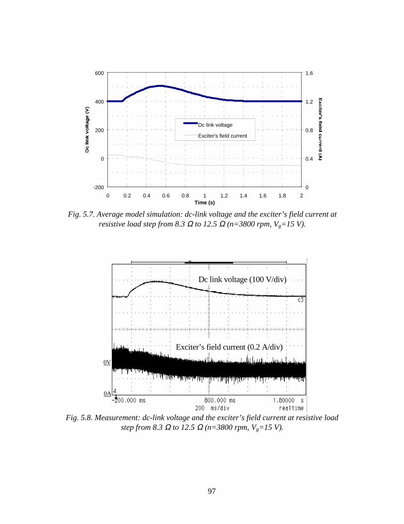
97
-200
0
200
400
600
0 0.2 0.4 0.6 0.8 1 1.2 1.4 1.6 1.8 2Time (s)
0
0.4
0.8
1.2
1.6
Dc link voltage
Exciter's field current
Fig. 5.7. Average model simulation: dc-link voltage and the exciter’s field current atresistive load step from 8.3 Ω to 12.5 Ω (n=3800 rpm, Vg=15 V).
0A
0V
Dc link voltage (100 V/div)
Exciter’s field current (0.2 A/div)
Fig. 5.8. Measurement: dc-link voltage and the exciter’s field current at resistive loadstep from 8.3 Ω to 12.5 Ω (n=3800 rpm, Vg=15 V).

98
5.2.3. Operation with inverter load and instability problem
After testing with resistive dc load, testing the closed loop system with inverter
connected to the dc-link was attempted. When that was done, instability occurred in the
form of oscillations of the dc-link voltage. This instability is due to the nature of the
inverter load, and can be explained in terms of the generator’s output impedance and the
inverter’s input impedance [22], [23].
A regulated inverter (i.e. an inverter operating in closed voltage loop) behaves like
a constant power load which, from the small-signal point of view, can be modeled as a
negative resistor, characterized by a phase of -180º. If such a load is connected to a non-
ideal voltage source, as shown in Fig. 5.9, it can be shown that the system will be stable if
21 io ZZ < .
(5.5)
Otherwise, there may be instability in the cascaded system, depending on the phase of the
ratio Zo1/Zi2.
Non-idealvoltage source
Constantpower load
Zo1 Zi2
Fig. 5.9. Illustration for instability problem.
Fig. 5.10 shows the generator’s output impedance (‘seen’ from the dc-link,
therefore including the dc-link capacitor) in open and closed loop. It can be seen that, at
frequencies up to the crossover frequency, closing the loop reduces the magnitude of the
generator’s output impedance by a factor approximately equal to the loop gain
magnitude. Around the crossover frequency, there is a certain peaking in closed loop
output impedance due to the small phase margin, which makes it somewhat higher than

99
the open loop output impedance. At frequencies significantly higher than the crossover
frequency, closing the loop has no effect on the output impedance.
-40
-30
-20
-10
0
10
20
30
40
50
60
0.01 0.1 1 10 100 1000Frequency (Hz)
Generator's open-loop Zo
Generator's closed-loop Zo
Inverter's closed-loop Zi
Fig. 5.10. Magnitude of the generator’s output impedance (in open and closed loop) andthe inverter’s input impedance (3340 rpm, 105 kW current source load).
Fig. 5.10 also shows input impedance of the inverter operating in closed voltage
loop at 105 kW output power level. It can be seen that the inverter’s input impedance
intersects with the generator’s closed-loop output impedance. Therefore, instability is
present in the system.
A solution to the instability problem consists in increasing the bandwidth of the dc-
link voltage loop. It can be predicted from the generator’s open-loop output impedance
plot in Fig. 5.10 that, if the dc-link voltage control-loop’s crossover frequency were
between ten Hz and 100 Hz, the generator’s closed loop output impedance would have its
peak between zero dB and ten dB, and would not intersect with the inverter’s input
impedance. That would stabilize the overall system.
With the above discussion in mind, the new control goal becomes to design a dc-
link voltage loop compensator that would provide a crossover frequency large enough to
make the generator’s closed-loop output impedance smaller, at all frequencies, than the
inverter’s input impedance.

100
5.3. Multiple-pole, multiple-zero compensators
5.3.1. Design
It can be seen from Fig. 5.1 that the phase of control-to-output transfer function is
the main cause of difficulties in achieving high crossover frequency. At 30 Hz (which is
approximately the frequency at which crossover is desired), the phase of control-to-
output transfer function is -270º. An additional phase lag of 90º will be introduced by the
compensator’s pole in the origin, necessary to have zero steady state error. That would
cause the loop gain’s phase to be -360º at the desired crossover frequency. In order to
stabilize the system, three zeros are needed in the compensator’s transfer function at
frequencies lower than the desired crossover. For the compensator to be a causal system,
there have to be at least as many poles as zeros in the compensator’s transfer function;
practical considerations, however, suggest that there be one more pole than zero, in order
to attenuate the high-frequency noise that may appear at the compensator’s input. That
finally results in a four-pole, three zero compensator. Poles (other than the one in origin)
need to be placed at frequencies as high as possible, in order to affect the loop gain’s
phase as little as possible below the crossover frequency. Zeros are placed between one
Hz and ten Hz by following a trial-and-error procedure, in order to obtain a loop gain’s
magnitude that decreases steadily with a slope of approximately 20 dB/decade, and a
phase which stays well above -180º up to the crossover frequency.
The simulation showed very good results with three compensator poles placed at 1
kHz, zeros at 1.5 Hz, 2 Hz and 10 Hz, and a gain of 584. The corresponding loop gain is
shown in Fig. 5.11, and the generator’s closed loop output impedance (together with the
inverter’s input impedance) in Fig. 5.12. It can be seen that crossover frequency is 100
Hz, with a phase margin of about 15 degrees. Such a low phase margin is acceptable
because the loop gain’s phase, right after the crossover, reaches a minimum of -167º and
then rises again. It eventually reaches -180º at a frequency higher than one kHz. Actually,

101
if only the phase of the loop gain had been considered, crossover frequency could have
been extended above 100 Hz. However, that would not have had the desired effect on the
control-loop because of the shape of the loop gain’s magnitude in the range of 200 Hz–1
kHz. As it is known, the control-loop is effective only as long as the loop gain’s
magnitude is much larger than one; that would not have been the case in the 200 Hz–1
kHz range with the magnitude shaped as in Fig. 5.11.
-50
0
50
100
150
0.01 0.1 1 10 100 1000Frequency (Hz)
Mag
nitu
de (
dB)
-180
-150
-120
-90
-60
Phase (deg)
Magnitude (dB)
Phase (degrees)
Fig. 5.11. Loop gain with four-pole, three-zero compensator (3340 rpm, 105 kW currentsource load).
It can be seen from Fig. 5.12 that, with a four-pole, three-zero compensator, the
generator’s closed loop output impedance always stays well below the inverter’s input
impedance. It could have been expected, therefore, that this compensator would have
solved the instability problem.
An analog four-pole, three-zero compensator was implemented using three stages
(three compensated operational amplifiers) connected in cascade. The first stage had a
gain of one, one pole at one kHz and one zero at ten Hz; the second stage had a gain also
equal to one, pole at one kHz and zero at two Hz; finally, the third stage had a gain of
584, one pole in the origin, one at one kHz, and one zero at 1.5 Hz. When tested, this
compensator revealed itself to be extremely sensitive to noise. The reason for that was the
fact that the first two stages, having one pole and one zero only, also had high, flat gain at

102
high frequencies, thus amplifying any noise that would appear at the compensator’s input.
The noise problems were serious enough to compromise entirely the operation of the
closed loop system.
-40
-30
-20
-10
0
10
20
30
40
50
0.01 0.1 1 10 100 1000Frequency (Hz)
Generator's closed loop Zo
Inverter's closed-loop Zi
Fig. 5.12. Generator’s closed loop output impedance with four-pole, three zerocompensator (3340 rpm, 105 kW current source load).
In order to solve the noise-related problems, implementation of the compensator,
and even the compensator itself, had to be changed. Instead of three stages, a two-stage
approach was tried. The first stage had gain of one, one zero and two poles, so that its
gain decreases at high frequencies. The second stage had two zeros and three poles (of
which one was in the origin). Therefore, one pole was added to the compensator to
reduce the high-frequency gain of the first stage. That resulted in a three-zero, five-pole
compensator. All poles that previously used to be at one kHz, had to be shifted at lower
frequencies, in order to decrease high-frequency gain of both stages. After several
attempts, it was found by trial-and-error that pole frequencies of 150 Hz, 150 Hz, 250 Hz
and 500 Hz made the noise effects tolerable. Frequencies at which compensator zeros
were placed remained unchanged. The highest-frequency zero (ten Hz) and lowest
frequency pole (150 Hz) were attributed to the first stage, in order to keep its gain as low
as possible at all frequencies. Decreasing pole frequencies required a decrease by a factor
of five (117 instead of 584) in the compensator’s gain (attributed entirely to the second
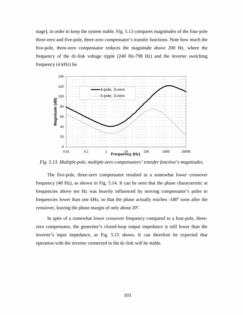
103
stage), in order to keep the system stable. Fig. 5.13 compares magnitudes of the four-pole
three-zero and five-pole, three-zero compensator’s transfer functions. Note how much the
five-pole, three-zero compensator reduces the magnitude above 200 Hz, where the
frequency of the dc-link voltage ripple (240 Hz-798 Hz) and the inverter switching
frequency (4 kHz) lie.
0
20
40
60
80
100
120
140
0.01 0.1 1 10 100 1000 10000Frequency (Hz)
Mag
nitu
de (
dB)
4-pole, 3-zero
5-pole, 3-zero
Fig. 5.13. Multiple-pole, multiple-zero compensators’ transfer function’s magnitudes.
The five-pole, three-zero compensator resulted in a somewhat lower crossover
frequency (40 Hz), as shown in Fig. 5.14. It can be seen that the phase characteristic at
frequencies above ten Hz was heavily influenced by moving compensator’s poles to
frequencies lower than one kHz, so that the phase actually reaches -180º soon after the
crossover, leaving the phase margin of only about 20º.
In spite of a somewhat lower crossover frequency compared to a four-pole, three-
zero compensator, the generator’s closed-loop output impedance is still lower than the
inverter’s input impedance, as Fig. 5.15 shows. It can therefore be expected that
operation with the inverter connected to the dc-link will be stable.
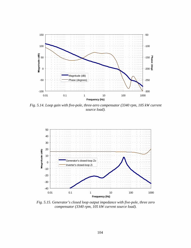
104
-100
-50
0
50
100
150
0.01 0.1 1 10 100 1000
Frequency (Hz)
-300
-250
-200
-150
-100
-50
Magnitude (dB)
Phase (degrees)
Fig. 5.14. Loop gain with five-pole, three-zero compensator (3340 rpm, 105 kW currentsource load).
-40
-30
-20
-10
0
10
20
30
40
50
0.01 0.1 1 10 100 1000Frequency (Hz)
Generator's closed-loop Zo
Inverter's closed-loop Zi
Fig. 5.15. Generator’s closed loop output impedance with five-pole, three zerocompensator (3340 rpm, 105 kW current source load).
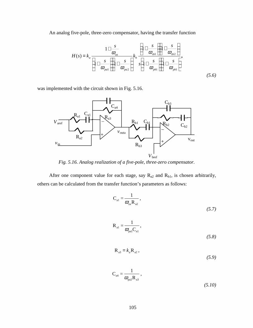
105
An analog five-pole, three-zero compensator, having the transfer function
+
+
+
+
+
+
+=
11
21
21
11
11
11
1
)(
pbpb
zbzbb
papa
zaa
sss
ss
kss
s
ksH
ωω
ωω
ωω
ω,
(5.6)
was implemented with the circuit shown in Fig. 5.16.
Ra1
Ra2
Ra3Ca1
Ca4
Rb1 Rb2
Rb3
Cb1
Cb3
Cb2
++
_
_Varef
vin
vout
Vbref
vouta
Fig. 5.16. Analog realization of a five-pole, three-zero compensator.
After one component value for each stage, say Ra2 and Rb1, is chosen arbitrarily,
others can be calculated from the transfer function’s parameters as follows:
a2zaa1 R
1=C
ω,
(5.7)
a1pa1a1 C
1=R
ω,
(5.8)
a2a3 RR ak= ,
(5.9)
a3pa2a4 R
1=C
ω,
(5.10)

106
b1pb2b1 R
1=C
ω,
(5.11)
b1zb2b3 C
1=R
ω,
(5.12)
bb3b2 kR
1=C ,
(5.13)
b2zb1b2 C
1=R
ω,
(5.14)
b2pb1b3 R
1=C
ω.
(5.15)
For (5.10)-(5.14) to be valid, it needs to be Cb2>>C b3 and Rb3>>Rb1.
5.3.2. Operation with resistive dc load
The five-pole, three-zero compensator was first tested with a resistive dc load. The
same transients presented in Section 5.2.2 for a PI compensator were simulated and
measured with a five-pole, three-zero compensator. The results are shown in Fig. 5.17-
Fig. 5.20. The time scale in these figures is the same as in Fig. 5.5-Fig. 5.8, relative to the
PI compensator. It can be seen that the increased control-loop’s bandwidth results in
dramatically decreased overshoot and settling time.
Fig. 5.21-Fig. 5.24 show resistive load step of the same magnitude as the one
shown in Fig. 5.17-Fig. 5.20, but of the opposite sign. Time scale is also more detailed, in
order to highlight the close matching of simulated and measured results.

107
-200
-100
0
100
200
300
400
500
600
-1.5 -1 -0.5 0 0.5 1 1.5 2 2.5 3 3.5Time (s)
0
0.2
0.4
0.6
0.8
1
1.2
1.4
1.6
Dc link voltage
Exciter's field current
Fig. 5.17. Average model simulation: the dc-link voltage and exciter’s field current for aresistive load step from 8.3 Ω to 12.5 Ω (n=2000 rpm, Vg=25 V).
Dc link voltage (100 V/div)
Exciter’s field current (0.2 A/div)
0V
0A
Fig. 5.18. Measurement: the dc-link voltage and exciter’s field current for a resistiveload step from 8.3 Ω to 12.5 Ω (n=2000 rpm, Vg=25 V).

108
-200
-100
0
100
200
300
400
500
600
0 0.2 0.4 0.6 0.8 1 1.2 1.4 1.6 1.8 2
Time (s)
0
0.2
0.4
0.6
0.8
1
1.2
1.4
1.6
Dc link voltage
Exciter's field current
Fig. 5.19. Average model simulation: the dc-link voltage and exciter’s field current for aresistive load step from 8.3 Ω to 12.5 Ω (n=3800 rpm, Vg=15 V).
Dc link voltage (100 V/div)
Exciter’s field current (0.2 A/div)
0V
0A
Fig. 5.20. Measurement: the dc-link voltage and exciter’s field current for a resistiveload step from 8.3 Ω to 12.5 Ω (n=3800 rpm, Vg=15 V).

109
-200
-100
0
100
200
300
400
500
600
0 0.05 0.1 0.15 0.2 0.25 0.3 0.35 0.4 0.45 0.5Time (s)
0
0.2
0.4
0.6
0.8
1
1.2
1.4
1.6
Dc link voltage
Exciter's field current
Fig. 5.21. Average model simulation: the dc-link voltage and exciter’s field current for aresistive load step from 12.5 Ω to 8.3 Ω (n=2000 rpm, Vg=25 V).
Dc link voltage (100 V/div)
Exciter’s field current (0.2 A/div)0V
0A
Fig. 5.22. Measurement: the dc-link voltage and exciter’s field current for a resistiveload step from 12.5 Ω to 8.3 Ω (n=2000 rpm, Vg=25 V).

110
-200
-100
0
100
200
300
400
500
600
0 0.02 0.04 0.06 0.08 0.1 0.12 0.14 0.16 0.18 0.2
Time (s)
0
0.2
0.4
0.6
0.8
1
1.2
1.4
1.6
Dc link voltage
Exciter's field current
Fig. 5.23. Average model simulation: the dc-link voltage and exciter’s field current for aresistive load step from 12.5 Ω to 8.3 Ω (n=3800 rpm, Vg=15 V).
Dc link voltage (100 V/div)
Exciter’s field current (0.2 A/div)
0V
0A
Fig. 5.24. Measurement: the dc-link voltage and exciter’s field current for a resistiveload step from 12.5 Ω to 8.3 Ω (n=3800 rpm, Vg=15 V).

111
5.3.3. Operation with inverter load
After the testing with a resistive load showed stable operation, fast transient
response and good matching of simulated and measured results, a five-pole, three zero
compensator was tested with the inverter connected to the dc-link. No instability was
detected in the system.
Fig. 5.25 and Fig. 5.26 show the dc-link voltage and exciter’s field current during
the transient caused by stepping the inverter’s resistive three-phase load from 12.8 kW to
18.8 kW. Due to the lack of damping at the dc-link, the response is slightly more
oscillatory than with resistive load; overshoot in dc-link voltage is, nevertheless, very
small.
It can be concluded, therefore, that a five-pole, three-zero compensator satisfies the
requirements regarding the system’s stability and the generator’s output impedance
damping.
Dc link voltage (100 V/div)
Exciter’s field current (0.5 A/div)
0V 0A
Fig. 5.25. Measurement: the dc-link voltage and exciter’s field current at step in theinverter’s resistive three-phase load from 18.8 kW to 12.8 kW (n=3000 rpm, Vg=35 V).

112
Dc link voltage (100 V/div)
Exciter’s field current (0.5 A/div)
0V 0A
Fig. 5.26. Measurement: the dc-link voltage and exciter’s field current at step in theinverter’s resistive three-phase load from 12.8 kW to 18.8 kW (n=3800 rpm, Vg=35 V).

113
Chapter 6. Conclusions
When a diode rectifier is supplied from a three-phase voltage source with large
internal impedance and/or is loaded with a reactive dc load, its operation cannot be
described with equations derived analytically assuming instantaneous commutations of
diodes. An example of a source which can cause extremely non-ideal operation of the
rectifier is a variable-speed stand-by synchronous generator, characterized by an
extremely large value of synchronous impedance as a consequence of variable-speed
design. This thesis presents an attempt to develop a simplified model of the system
consisting of a synchronous generator with large internal impedance feeding a diode
rectifier with a reactive dc load. The results obtained, however, go beyond this particular
application, and can be applied to any case in which the source’s impedance significantly
affects operation of the diode rectifier.
The basis for the development of the simplified, average generator/rectifier model
consists of the study of the generator’s ac waveforms affected by the non-ideal operation
of the diode bridge and reactive nature of the dc load. This study is carried out through
analysis of the switching model of the system. It can be concluded from such analysis
that there exists a phase shift between the fundamental harmonics of the generator’s
voltage and current. In the ideal case, when commutations of the rectifier’s diodes are
instantaneous, this phase shift is equal to zero. Also, average values of dc current and
voltage at the rectifier’s output are found to be different than in the ideal case. The
amount of phase shift and discrepancies in average values of the dc variables depend on
114
the parameters of the three-phase source (in the studied case, the synchronous generator),
and the nature of the dc load (capacitive or inductive). They affect both transient and
steady state operation of the system, and need to be taken into account when, for
example, the system’s control-loops are designed.
The developed average model of the diode rectifier relies on the assumption that
fundamental harmonic of ac variables and average value of dc variables are of primary
importance for the system’s operation, as far as power transfer and dynamic behavior is
concerned. This assumption is true in most practical applications, due to the primarily
inductive character of the source’s impedance and presence of a filter at rectifier’s output.
The developed model allows us to relate the dynamics of the three-phase source
connected to the rectifier’s input, to dynamics of the reactive dc load at rectifier’s output.
In doing so, the non-ideal operation of the rectifier is taken into account by means of
three constants obtained from the switching model. These three constants model the
diode rectifier in an average sense, i.e. they make it possible to establish a relationship
between fundamental harmonics of ac voltage and current at the rectifier’s input to
average values of dc voltage and current at the rectifier’s output. The dependence of these
constants on the operating point is not highly pronounced, which results in the model’s
validity for both steady state and transient operation. This is verified to be true through
comparison of the average model simulation results with switching model simulation
results and measurement results, for both open- and closed-loop operation and different
operating points.
The way the average model is implemented takes into account losses in the diode
rectifier, and allows us to relate these losses directly to the average model’s parameters. If
diode losses are negligible, it can be shown that there are only two independent average
model’s parameters, from which the third one can be computed.
The main advantages of the average model, as opposed to the switching model, are
savings in computational time when time-domain simulations are performed, and the
possibility to perform frequency-domain analysis of the system. The latter is the result of
the average model’s equations’ being time-continuous and, therefore, easy to linearize.
From linearized equations, it is possible to obtain state-space representation and transfer

115
functions of the system. In the studied case, practical interest was focused on the exciter’s
field voltage-to-dc-link voltage transfer function, which represents the system’s control-
to-output transfer function. Dependence of this transfer function on the operating point
and nature of dc load was discussed from the point of view of dc-link voltage control-
loop design.
Design of this control-loop is a good example of a practical application of the
developed model. Control-to-output transfer function, obtained with the average
generator/rectifier model, shows that the actual order of the system in this case is such
that the often-used, first-order generator model cannot be applied. That is particularly true
if a high-order (five pole, three-zero) dynamic compensator needs to be designed in order
to stabilize the cascaded generator-rectifier-inverter system, affected by instability due to
poor matching of output and input impedances of different parts of the system. In such a
design, the system’s dynamic response needs to be known, in a detailed manner, at
frequencies much higher than the frequency corresponding to the transfer function’s
dominant pole. The developed average generator/rectifier model represents a unique and
indispensable means to study and solve this and similar problems.

116
References
[1] J. G. Kassakian, M. F. Schlecht and G. C. Verghese, Principles of Power Electronics,
Addison-Wesley Publishing Company, 1991.
[2] W. J. Bonwick and V. H. Jones, “Performance of a synchronous generator with a
bridge rectifier,” Proceedings IEE, Vol. 119, No. 9, September 1972, pp. 1338-1342.
[3] W. J. Bonwick and V. H. Jones, “Rectifier-loaded synchronous generator with
damper windings,” Proceedings IEE, Vol. 120, No. 6, June 1973, pp. 659-666.
[4] V. H. Jones and W. J. Bonwick, “Three-phase bridge rectifiers with complex source
impedance,” Proceedings IEE, Vol. 122, No. 6, June 1975, pp. 630-636.
[5] W. J. Bonwick, “Characteristics of a diode-bridge-loaded synchronous generator
without damper windings,” Proceedings IEE, Vol. 122, No. 6, June 1975, pp. 637-
641.
[6] W. J. Bonwick, “Voltage waveform distortion in synchronous generators with
rectifier loading,” IEE Proceedings, Vol. 127, Pt. B, No. 1, January 1980, pp. 13-19.
[7] R. L. Ames, “A.C. Generators: Design and Applications,” Research Studies Press
Ltd., Taunton, Somerset, England, 1990
[8] P. C. Krause, Analysis of Electric Machinery, New York: McGraw Hill, Inc., 1987.
[9] M. Jadric, Dinamika elektricnih strojeva, Graphis, Zagreb, 1997.
[10] PSpice A/D Reference Manual, Version 8.0, MicroSim Corporation, June 1997.

117
[11] A.H.M.S. Ula and Abul R. Hasan, “Design and Implementation of a Personal
Computer Based Automatic Voltage Regulator for a Synchronous Generator,” IEEE
Transactions on Energy Conversion, Vol. 7, No.1, March 1992, pp. 125-130.
[12] A. Ghandakly and P. Kronneger, “Digital Controller Design Method for
Synchronous Generator Excitation and Stabilizer Systems, Parts I and II,” IEEE
Transactions on Power Systems, Vol. PWRS-2, No. 3, August 1987, pp. 633-644.
[13] Y. Takeda and B. Adkins, “Determination of synchronous-machine parameters
allowing for unequal mutual inductances,” Proceedings IEE, Vol. 121, No. 12,
December 1974, pp. 1501-1504.
[14] M. E. Coultes and W. Watson, “Synchronous Machine Models by Standstill
Frequency Response Tests,” IEEE Transactions on Power Apparatus and Systems,
Vol. PAS-100, No. 4, April 1981, pp. 1480-1489.
[15] P. L. Dandeno and A. T. Poray, “Development of a Detailed Turbogenerator
Equivalent Circuit from Standstill Frequency Response Measurement,” IEEE
Transactions on Power Apparatus and Systems, Vol. PAS-100, No. 4, April 1981, pp.
1646-1655.
[16] S. H. Minnich, “Snall Signals, Large Signals, and Saturation in Generator
Modeling,” IEEE Transactions on Energy Conversion, Vol. EC-1, No. 1, March
1986, pp. 94-102.
[17] IEEE Standard Procedures for Obtaining Synchronous Machine Parameters by
Standstill Frequency Response Testing, IEEE Std. 115A-1987.
[18] A. Keyhani, H. Tsai and T. Leksan, “Maximum Likelihood Estimation of
Synchronous Machine Parameters from Standstill Time Response Data,” IEEE
Transaction on Energy Conversion, Vol. 9, No. 1, March 1994, pp. 98-114.
[19] A. Keyhani, H. Tsai, “Identification of High-Order Synchronous Generator
Models from SSFR Test Data,” IEEE Transactions on Energy Conversion, Vol. 9,
No. 3, September 1994, pp. 593-603.
[20] P. C. Krause and T. A. Lipo, “Analysis and Simplified Representations of
Rectifier-Inverter Induction Motor Drives,” IEEE Transactions on Power Apparatus
and Systems, Vol. PAS-88, No. 5, May 1969, pp. 588-596.

118
[21] P. C. Krause and T. A. Lipo, “Analysis and Simplified Representations of
Rectifier-Inverter Reluctance-Synchronous Motor Drives,” IEEE Transactions on
Power Apparatus and Systems, Vol. PAS-88, No. 6, June 1969, pp. 962-970.
[22] R. D. Middlebrook, “Input Filter Considerations in Design and Applications of
Switching Regulators,” IEEE IAS Annual Meeting, Chicago, IL, October 11-14, 1976.
[23] B. H. Cho, “Modeling and Analysis of Spacecraft Power Systems,” Ph.D.
Dissertation, Virginia Polytechnic Institute and State University, Blacksburg,
Virginia, October 1985.
119
Vita
Ivan Jadric
Ivan Jadric is a native of Split, Croatia. From 1989 to 1991 he studied at the
Faculty of Electrical Engineering, University of Zagreb, in Zagreb, Croatia, and from
1991 to 1995 at the Polytechnic of Turin in Turin Italy. He obtained the BS in Electrical
Engineering from the Polytechnic of Turin in July 1995. From August 1995 to January
1998, he was with the Virginia Power Electronics Center at Virginia Tech in Blacksburg,
Virginia, working towards the MS degree in Electrical Engineering. He is currently with
the York International Corporation in York, Pennsylvania.