Embed Size (px)
Citation preview
Modeling and Design of high
speed SRAM based Memory Chip
A Thesis submitted in partial fulfillment of the Requirements for the degree of
Master of Technology
In
Electronics and Communication Engineering
Specialization: VLSI Design & Embedded System
By
Rakesh chandankhede
Roll No.: 212EC2132
Department of Electronics and Communication Engineering
National Institute of Technology, Rourkela
Rourkela, Odisha, India, 769008
May 2014
Modeling and Design of high
speed SRAM based Memory Chip
A Thesis submitted in partial fulfillment of the Requirements for the degree of
Master of Technology In
Electronics and Communication Engineering
Specialization: VLSI Design & Embedded System
By
Rakesh Chandankhede
Roll No.: 212EC2132
Under the Guidance of
Prof. Debiprasad Priyabrata Acharya
Department of Electronics and Communication Engineering
National Institute of Technology, Rourkela
Rourkela, Odisha, India, 769008
May 2014

Dedicated to…
My Dear Friends
My parents and my sisters
DEPT. OF ELECTRONICS AND COMMUNICATION
ENGINEERING
NATIONAL INSTITUTE OF TECHNOLOGY, ROURKELA
ROURKELA, ODISHA, INDIA – 769008
Certificate
This is to certify that the work in the thesis entitled Modeling and Design of high speed
SRAM based Memory Chip by Rakesh Chandankhede is a record of an original
research work carried out by him during the 2013 - 2014 under my supervision and
guidance in partial fulfillment of the requirements for the award of the degree of Master of
Technology in Electronics and Communication Engineering (VLSI Design & Embedded
System), National Institute of Technology, Rourkela. Neither this thesis nor any part of it,
to the best of my knowledge, has been submitted for any degree or diploma elsewhere.
Place:
Date:
Prof. D. P. Acharya
Dept. of Electronics and Communication Engg.
National Institute of Technology
Rourkela-769008

DEPT. OF ELECTRONICS AND COMMUNICATION
ENGINEERING
NATIONAL INSTITUTE OF TECHNOLOGY, ROURKELA
ROURKELA, ODISHA, INDIA – 769008
Declaration I certify that
a) The work contained in the thesis is original and has been done by myself under the
general supervision of my supervisor.
b) The work has not been submitted to any other Institute for any degree or diploma.
c) I have followed the guidelines provided by the Institute in writing the thesis.
d) Whenever I have used materials (data, theoretical analysis, and text) from other
sources, I have given due credit to them by citing them in the text of the thesis and
giving their details in the references.
e) Whenever I have quoted written materials from other sources, I have put them
under quotation marks and given due credit to the sources by citing them and giving
the required details in the references.
Rakesh Chandankhede
30th May 2014

i
ACKNOWLEDGEMENTS
It is my immense pleasure to avail this opportunity to express my gratitude, regards and
heartfelt respect to Prof. D. P. Acharya, Department of Electronics and Communication
Engineering, NIT Rourkela for his endless and valuable guidance prior to, during and
beyond the tenure of the project work. His priceless advices have always lighted up my
path whenever I have struck a dead end in my work. It has been a rewarding experience
working under his supervision as he has always delivered the correct proportion of
appreciation and criticism to help me excel in my field of research.
I would also like to thank Mr. Pradip Patra, from Sankalp Semiconductor Pvt. Ltd. for
giving comprehensive knowledge on SRAM and providing me with his suggestion time to
time.
I would like to express my gratitude and respect to Prof. K. K. Mahapatra, Prof. S. K.
Patra, Prof. S. Meher, Prof. A. K. Swain, Prof. M. N. Islam and Prof. P. K. Tiwari for their
support, feedback and guidance throughout my M. Tech course duration. I would also like
to thank all the faculty and staff of the ECE department, NIT Rourkela for their support and
help during the two years of my student life in the department.
I am also very thankful to all my classmates and seniors of VLSI lab, especially Mr.
Tom, Mr. Jaganath, Mr. Debasish Nayak, Mr. Umakanta Nanda and all my friends who
always encouraged me in the Successful completion of my thesis work.
Rakesh chandankhede
ii
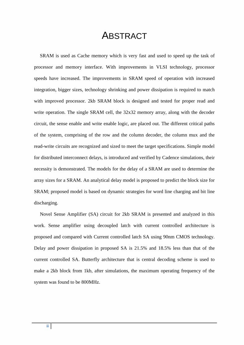
ABSTRACT
SRAM is used as Cache memory which is very fast and used to speed up the task of
processor and memory interface. With improvements in VLSI technology, processor
speeds have increased. The improvements in SRAM speed of operation with increased
integration, bigger sizes, technology shrinking and power dissipation is required to match
with improved processor. 2kb SRAM block is designed and tested for proper read and
write operation. The single SRAM cell, the 32x32 memory array, along with the decoder
circuit, the sense enable and write enable logic, are placed out. The different critical paths
of the system, comprising of the row and the column decoder, the column mux and the
read-write circuits are recognized and sized to meet the target specifications. Simple model
for distributed interconnect delays, is introduced and verified by Cadence simulations, their
necessity is demonstrated. The models for the delay of a SRAM are used to determine the
array sizes for a SRAM. An analytical delay model is proposed to predict the block size for
SRAM; proposed model is based on dynamic strategies for word line charging and bit line
discharging.
Novel Sense Amplifier (SA) circuit for 2kb SRAM is presented and analyzed in this
work. Sense amplifier using decoupled latch with current controlled architecture is
proposed and compared with Current controlled latch SA using 90nm CMOS technology.
Delay and power dissipation in proposed SA is 21.5% and 18.5% less than that of the
current controlled SA. Butterfly architecture that is central decoding scheme is used to
make a 2kb block from 1kb, after simulations, the maximum operating frequency of the
system was found to be 800MHz.
iii
CONTENTS
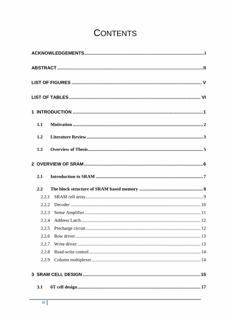
ACKNOWLEDGEMENTS .............................................................................................. I
ABSTRACT .................................................................................................................. II
LIST OF FIGURES ...................................................................................................... V
LIST OF TABLES ....................................................................................................... VI
1 INTRODUCTION ...................................................................................................... 1
1.1 Motivation .................................................................................................................. 2
1.2 Literature Review ...................................................................................................... 3
1.3 Overview of Thesis ..................................................................................................... 5
2 OVERVIEW OF SRAM ............................................................................................. 6
2.1 Introduction to SRAM .............................................................................................. 7
2.2 The block structure of SRAM based memory ........................................................ 8
2.2.1 SRAM cell array ....................................................................................................... 9
2.2.2 Decoder .................................................................................................................. 10
2.2.3 Sense Amplifier ...................................................................................................... 11
2.2.4 Address Latch ......................................................................................................... 12
2.2.5 Precharge circuit ..................................................................................................... 12
2.2.6 Row driver .............................................................................................................. 13
2.2.7 Write driver ............................................................................................................ 13
2.2.8 Read-write control .................................................................................................. 14
2.2.9 Column multiplexer ................................................................................................ 14
3 SRAM CELL DESIGN ............................................................................................ 15
3.1 6T cell design ............................................................................................................ 17
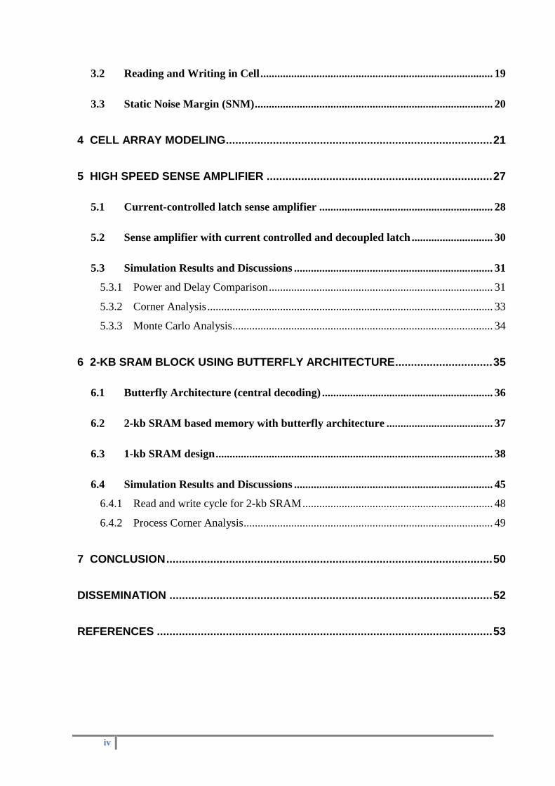
iv
3.2 Reading and Writing in Cell ................................................................................... 19
3.3 Static Noise Margin (SNM) ..................................................................................... 20
4 CELL ARRAY MODELING ..................................................................................... 21
5 HIGH SPEED SENSE AMPLIFIER ........................................................................ 27
5.1 Current-controlled latch sense amplifier .............................................................. 28
5.2 Sense amplifier with current controlled and decoupled latch ............................. 30
5.3 Simulation Results and Discussions ....................................................................... 31
5.3.1 Power and Delay Comparison ................................................................................ 31
5.3.2 Corner Analysis ...................................................................................................... 33
5.3.3 Monte Carlo Analysis ............................................................................................. 34
6 2-KB SRAM BLOCK USING BUTTERFLY ARCHITECTURE ............................... 35
6.1 Butterfly Architecture (central decoding) ............................................................. 36
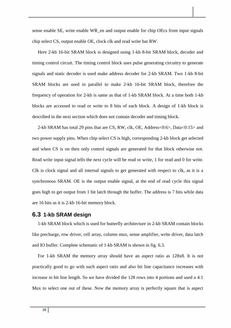
6.2 2-kb SRAM based memory with butterfly architecture ...................................... 37
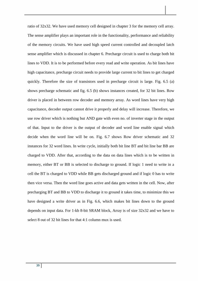
6.3 1-kb SRAM design ................................................................................................... 38
6.4 Simulation Results and Discussions ....................................................................... 45
6.4.1 Read and write cycle for 2-kb SRAM .................................................................... 48
6.4.2 Process Corner Analysis ......................................................................................... 49
7 CONCLUSION ........................................................................................................ 50
DISSEMINATION ....................................................................................................... 52
REFERENCES ........................................................................................................... 53
v
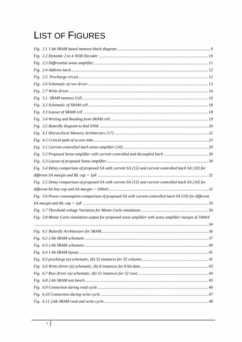
LIST OF FIGURES Fig. 2.1 1-kb SRAM based memory block diagram ........................................................................................... 9
Fig. 2.2 Dynamic 2 to 4 NOR Decoder ........................................................................................................... 10
Fig. 2.3 Differential sense amplifier ................................................................................................................ 11
Fig. 2.4 Address latch...................................................................................................................................... 12
Fig. 2.5 Precharge circuit .............................................................................................................................. 12
Fig. 2.6 Schematic of row driver ..................................................................................................................... 13
Fig. 2.7 Write driver ........................................................................................................................................ 14
Fig. 3.1 SRAM memory Cell ........................................................................................................................... 16
Fig. 3.2 Schematic of SRAM cell ..................................................................................................................... 18
Fig. 3.3 Layout of SRAM cell .......................................................................................................................... 18
Fig. 3.4 Writing and Reading from SRAM cell ................................................................................................ 19
Fig. 3.5 Butterfly diagram to find SNM ........................................................................................................... 20
Fig. 4.1 Hierarchical Memory Architecture [17] ............................................................................................ 22
Fig. 4.2 Critical path of access time ................................................................................................................ 23
Fig. 5.1 Current-controlled latch sense amplifier [10] ................................................................................... 29
Fig. 5.2 Proposed Sense amplifier with current controlled and decoupled latch ........................................... 30
Fig. 5.3 Layout of proposed Sense amplifier ................................................................................................... 30
Fig. 5.4 Delay comparison of proposed SA with current SA [15] and current controlled latch SA [10] for
different SA margin and BL cap = 1pF ............................................................................................................ 32
Fig. 5.5 Delay comparison of proposed SA with current SA [15] and current controlled latch SA [10] for
different bit line cap and SA margin = 100mV ................................................................................................. 32
Fig. 5.6 Power consumption comparison of proposed SA with current controlled latch SA [10] for different
SA margin and BL cap = 1pF .......................................................................................................................... 33
Fig. 5.7 Threshold voltage Variation for Monte Carlo simulation ................................................................. 34
Fig. 5.8 Monte Carlo simulation output for proposed sense amplifier with sense amplifier margin of 100mV
.......................................................................................................................................................................... 34
Fig. 6.1 Butterfly Architecture for SRAM ........................................................................................................ 36
Fig. 6.2 2-kb SRAM schematic ........................................................................................................................ 37
Fig. 6.3 1-kb SRAM schematic ........................................................................................................................ 40
Fig. 6.4 1-kb SRAM layout .............................................................................................................................. 41
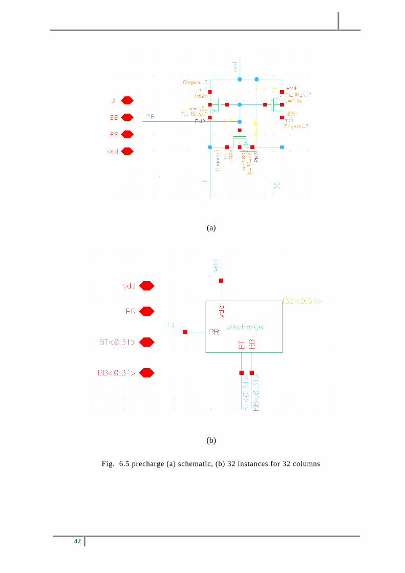
Fig. 6.5 precharge (a) schematic, (b) 32 instances for 32 columns ................................................................ 42
Fig. 6.6 Write driver (a) schematic, (b) 8 instances for 8 bit data .................................................................. 43
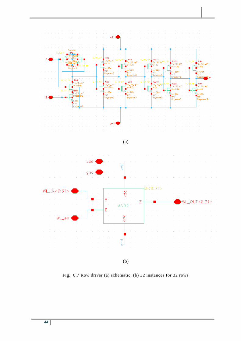
Fig. 6.7 Row driver (a) schematic, (b) 32 instances for 32 rows .................................................................... 44
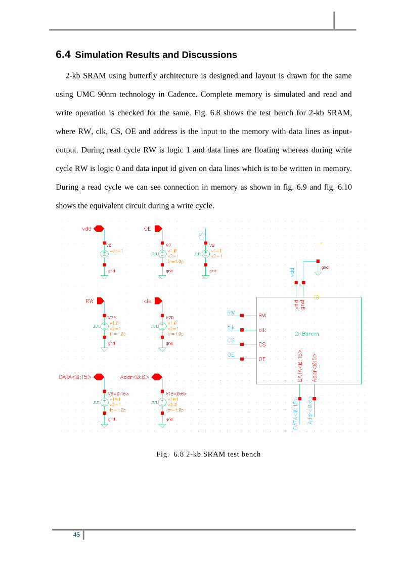
Fig. 6.8 2-kb SRAM test bench ........................................................................................................................ 45
Fig. 6.9 Connection during read cycle ............................................................................................................ 46
Fig. 6.10 Connection during write cycle ......................................................................................................... 47
Fig. 6.11 2-kb SRAM read and write cycle...................................................................................................... 48
vi
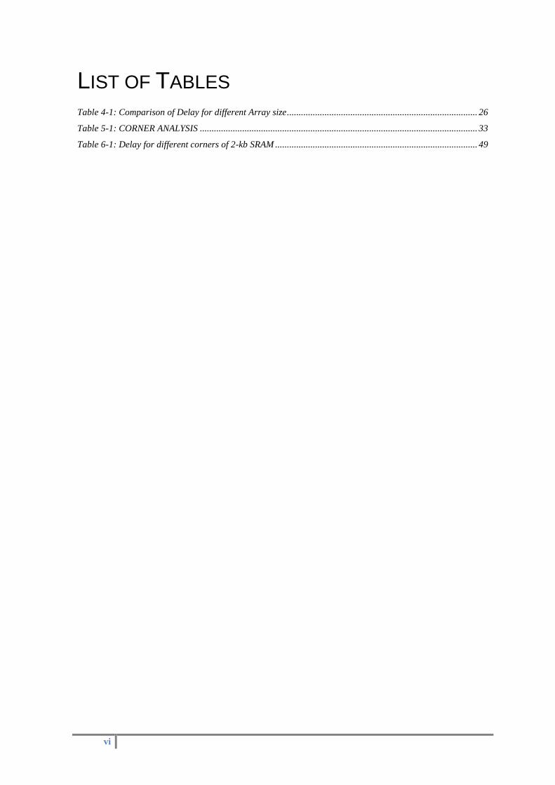
LIST OF TABLES Table 4-1: Comparison of Delay for different Array size ................................................................................. 26
Table 5-1: CORNER ANALYSIS ...................................................................................................................... 33
Table 6-1: Delay for different corners of 2-kb SRAM ...................................................................................... 49
1
1
INTRODUCTION
2
SRAM is used as Cache memory which is very fast and used to speed up the task of
processor and memory interface. With the recent improvements in VLSI technology,
processor speeds have increased intensely. To take the advantage of high speed processors,
i.e. high clock rates, need to provide instructions and data to the processor with little or no
delay. Therefore the very high frequency is required for instructions and data. With
improvements in VLSI technology, the speed of the logic gates has increased significantly,
but memory speed is not improved equivalently because memory densities have increased
simultaneously. Therefore, for high speed computers, SRAM memories are very important
to improve speed and can be used with processors to do so. In this work we have
concentrated on the design of high speed SRAM which can be used as high speed memory
for high speed computers.
1.1 Motivation
Intel microprocessor family demonstrates that the on chip cache sizes in microprocessor
is increasing with increase in speed, on chip L2 (level two) cache size in Intel’s Pentium III
Coppermine is increased from 256 KB, to 4 MB in Intel’s core i3 processor, to 8 MB in
Intel core i7-920 processor with 2.66 GHz clock frequency [18]. Also in Smart phones
processor on chip cache sizes of Qualcomm’s Snapdragon processor family shows L2
(level two) cache sizes increasing, from 256KB in Qualcomm QSD8250 with 65-nm
technology, to 1MB in Qualcomm Snapdragon S4:MSM8960 with 1.3 GHz clock
frequency [19].
For high performance microprocessors and SoC (system-on-chip) implementations
bigger sized on chip caches are necessary. These large sizes are made up by the small
SRAM memory blocks which respond to very high frequency. The SRAM memory blocks
are nothing but the array of memory cells, in which cells are placed in the way such that bit
line and word line delay due to the interconnection and parasitic capacitance will be low.
3
Moreover, with technology reduces by a factor of 2 in every 18 months, In comparison
with transistor, interconnects are getting worse [9], as transistor sizes shrinks and SRAM
size increases, distributed interconnects delay dominates SRAM character. Precise SRAM
performance assessments require exact calculations of interconnect delay. If the designer is
willing to compare different architectures for a memory array so that the desired
specifications will get fulfilled, it will be tedious to draw the layout of every possible
architecture and check the performance, fast and sensibly correct calculations are required
during the initial stage of design to overcome this problem.
Low power, high speed SRAMs are very important element of many VLSI chips. It is
particularly true for microprocessors, in microprocessors, to bridge the growing deviation
in speed of processor and memory, with each generation the on chip cache sizes are
increasing. Also, due to increased integration, speed of operation and explosive
development of battery operated appliances; power dissipation is an important concern.
High speed of operation with increased integration, bigger sizes, technology shrinking
and power dissipation in SRAM motivates to concentrate on these areas for improved
SRAM memory.
1.2 Literature Review
• Dr. Robert H. Dennard, in 1966, created the one transistor DRAM. He used a single
transistor and a capacitor to make a simpler memory cell. Dr. Dennard with IBM granted a
patent for DRAM in 1968. Fairchild Corporation developed first 256-k SRAM chip in
1970. [20]
• Kenneth and Amrutur [7] presented SRAM using a half swing pulse mode gate
family; it does not affect performance though it is using reduced input signal swing. As it
reduces the signal swing on bit lines, word lines and predecode lines, this SRAM is having
very less power dissipation.
4
• Wada et al. [2] have considered configuration, organization, and process parameters
for formulation of the access time of on chip cache. The limitations of this model are, it
doesn’t consider interconnect delays and tag paths, for each delay stage it assumes a step
input waveform, and overgeneralized delay models and circuit models.
• Jouppi and Wilton [3] have stretched Wada’s model to develop new model CACTI.
It shows how different cache organizations affect access time. They have stretched the
results to submicron technology nodes using linear scaling of delay; this method may be
inaccurate to predict performance of the recent submicron cache design.
• Amrutur and Horowitz [4] have given a model for area, delay and power of SRAM.
They have considered that wire delay affects access speed of SRAM. They considered that
with technology shrinking we need to redesign wires to retain the delay of wire in the
proportion of the gate delay.
• Annie Zeng et al. [5] have developed predictor of access and cycle time for cache
stack (PRACTICS) for on chip cache. It considers both dynamic power and delay models.
To predict performance of large cache memory in submicron technology nodes, appropriate
circuit structures, improved wire delay, and technology dependent parameters are
necessary.
• Tsuguo Kobayashi [10] has proposed a current controlled sense amplifier which
gives improvement over Teruo Seki’s [11] Latched Sense Amplifier in term of power
dissipation and performance. It does not require any decoupling at its input, reason for that
it has high impedance input differential stage, which avoids lower noise margin due to the
added pass‑gate transistors which leads to a voltage drop that declines the available input
voltage difference.
5
1.3 Overview of Thesis
This thesis carries out the modeling and design of high speed SRAM based memory.
The overview of SRAM is provided in Chapter 2 of the thesis. Chapter 3 describes 6T
SRAM cell design. The Memory array design and analytical access time model for on-chip
SRAM memories which shows the dependence of the SRAM access time on the
parameters like number of rows N and columns M are discussed in Chapter 4. Chapter 5
describes novel sense amplifier (SA) circuit for SRAM. Sense amplifier using decoupled
latch with current controlled architecture is proposed and compared with current controlled
latch SA in this chapter. After all the design of the complete 2-kb SRAM block and its
simulation results are discussed in chapter 6. Chapter 7 gives the conclusion of the work
done.
6
2
OVERVIEW OF SRAM
7
Static Random Access Memory (SRAM) to store each bit uses bi-stable latching
circuitry. The term static in static random access memory differentiates it from dynamic
random access memory (DRAM) which needs to be refreshed periodically. SRAM is
volatile that data is eventually lost when memory is not powered. This chapter gives an
overview of SRAM in that Section 2.1 discuss about types, uses and operation of SRAM
and Block structure of SRAM giving an insight view of circuits for SRAM memory
presented in section 2.2.
2.1 Introduction to SRAM
Depending on the use of a clock, SRAM can be divided as synchronous SRAM and
asynchronous SRAM. In synchronous SRAM, all the internal signals and timing will be
controlled by clock edge. Data in, control signals as well as address relates to the clock
signal, it is mostly used as cache memory. While asynchronous SRAM is independent of
clock frequency. All the internal signals and timings are initialized by the address
transition. The size of asynchronous SRAM varies from 4 Kb to 64 Mb. Due to the fast
access time of asynchronous SRAM, it is suitable as main memory for cache less
embedded processors which are used in industrial electronics, networking equipment, hard
disks, measurement systems,. It is also used in applications like IP-Phones, IC-Testers,
switches and routers, DSLAM Cards and Automotive Electronics.
SRAM is used in embedded systems such as digital cameras, automotive electronics,
cell phones, synthesizers, LCD screens and printers. In computers, routers and peripherals,
workstations, it is used as CPU register files, hard disk buffers, internal CPU caches and
external burst mode SRAM caches, router buffers, hard disk buffers, etc.
The operation of SRAM can be divided into three states, first is Standby mode, in
which word line is not activated, thus address and data lines are kept detached from SRAM
8
memory cells, hence cells keep the data as it is and no read and write operation is there.
Power dissipation in this mode is the lowest. A second mode of operation is reading from
SRAM, suppose we are reading from a cell which has logic 1 stored in it. Read cycle starts
with precharging the bit line and bit line bar, after precharge word line gets activated
according to address input and one of the bit line start discharging through the cell. Here
logic 1 is stored so bit line bar will start discharging. Sense amplifier senses the difference
in voltage on bit line and bit line bar and gives the proper output. The high sensitivity of
sense amplifier, smaller the read access time. The next mode of operation of SRAM is
writing into the SRAM cell. Write operation starts with applying the data input need to be
written on bit lines. Suppose we have to write 1, the bit line will get charged to 1 and bit
line bar will need to discharge to 0. Then the word line will get activated, and appropriate
data gets written to the cell that is SRAM memory. Proper sizing needs to be done for
accurate reading and writing operation, also static noise margin need to be more so that in
the standby mode cell will tolerate the noise.
2.2 The block structure of SRAM based memory
Fig. 2.1 shows 1-kb SRAM block structure which includes Cell Array, decoder, sense
amplifier, write driver, column mux, precharge circuitry, address latch and read and write
control as the peripheral circuit to the SRAM cell array. Since the memory core trade
performance and reliability in reduction area, memory design relies exceedingly on the
peripheral circuitry to recover both speed and electrical integrity. While the design of the
core is dominated by technological consideration and is largely beyond the scope of the
circuit designer, it is in the design of the periphery where a good designer can make an
important difference.
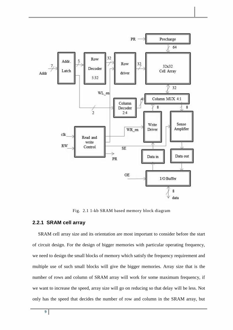
9
Fig. 2.1 1-kb SRAM based memory block diagram
2.2.1 SRAM cell array
SRAM cell array size and its orientation are most important to consider before the start
of circuit design. For the design of bigger memories with particular operating frequency,
we need to design the small blocks of memory which satisfy the frequency requirement and
multiple use of such small blocks will give the bigger memories. Array size that is the
number of rows and column of SRAM array will work for some maximum frequency, if
we want to increase the speed, array size will go on reducing so that delay will be less. Not
only has the speed that decides the number of row and column in the SRAM array, but
10
aspect ratio also needed to be considered. 1:1 is the perfect aspect ratio of no. of rows to
column. Suppose, for 1-Mb 8-bit SRAM memory, 1-kb is block we are using so that
operating frequency will be very high. Therefore, for 1kb SRAM the memory array should
have an aspect ratio as 128x8. It is not practically good to go with such aspect ratio and
also bit line capacitance increases with increase in bit line length. So we have divided the
128 rows into 4 portions and used a 4:1 Mux to select one out of these. Now the memory
array is perfectly square that is aspect ratio of 32x32. How to decide the array size for a
particular frequency is described in chapter 4 using mathematical models.
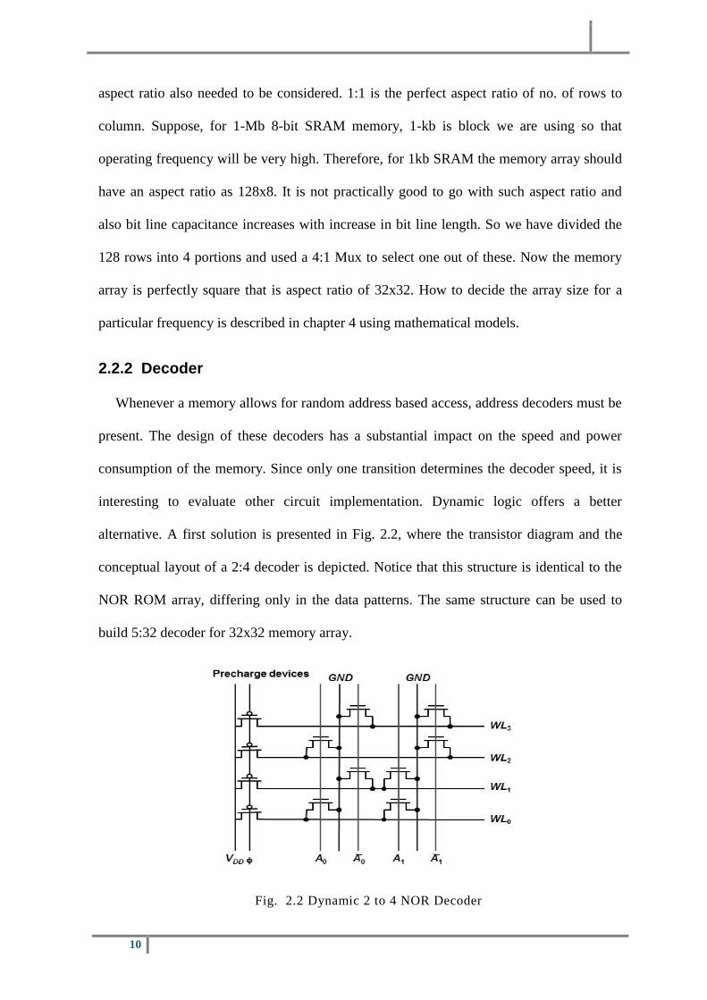
2.2.2 Decoder
Whenever a memory allows for random address based access, address decoders must be
present. The design of these decoders has a substantial impact on the speed and power
consumption of the memory. Since only one transition determines the decoder speed, it is
interesting to evaluate other circuit implementation. Dynamic logic offers a better
alternative. A first solution is presented in Fig. 2.2, where the transistor diagram and the
conceptual layout of a 2:4 decoder is depicted. Notice that this structure is identical to the
NOR ROM array, differing only in the data patterns. The same structure can be used to
build 5:32 decoder for 32x32 memory array.
Fig. 2.2 Dynamic 2 to 4 NOR Decoder
11
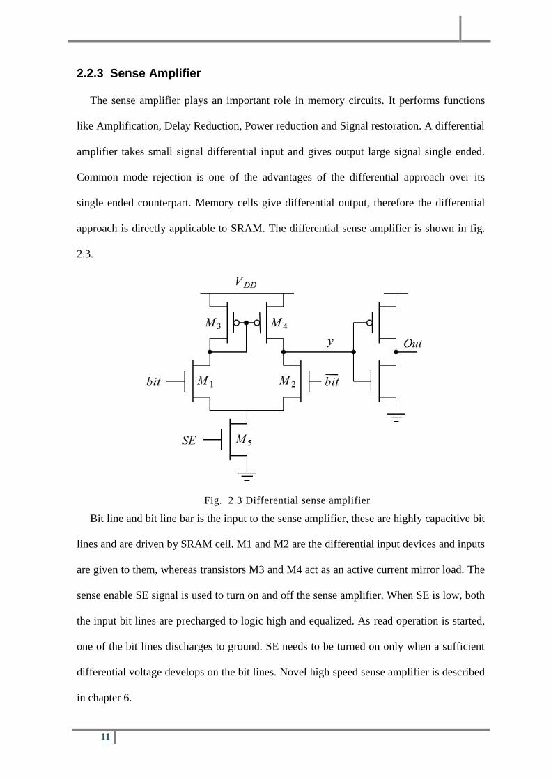
2.2.3 Sense Amplifier
The sense amplifier plays an important role in memory circuits. It performs functions
like Amplification, Delay Reduction, Power reduction and Signal restoration. A differential
amplifier takes small signal differential input and gives output large signal single ended.
Common mode rejection is one of the advantages of the differential approach over its
single ended counterpart. Memory cells give differential output, therefore the differential
approach is directly applicable to SRAM. The differential sense amplifier is shown in fig.
2.3.
Fig. 2.3 Differential sense amplifier
Bit line and bit line bar is the input to the sense amplifier, these are highly capacitive bit
lines and are driven by SRAM cell. M1 and M2 are the differential input devices and inputs
are given to them, whereas transistors M3 and M4 act as an active current mirror load. The
sense enable SE signal is used to turn on and off the sense amplifier. When SE is low, both
the input bit lines are precharged to logic high and equalized. As read operation is started,
one of the bit lines discharges to ground. SE needs to be turned on only when a sufficient
differential voltage develops on the bit lines. Novel high speed sense amplifier is described
in chapter 6.
12
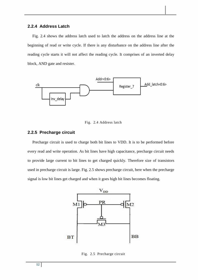
2.2.4 Address Latch
Fig. 2.4 shows the address latch used to latch the address on the address line at the
beginning of read or write cycle. If there is any disturbance on the address line after the
reading cycle starts it will not affect the reading cycle. It comprises of an inverted delay
block, AND gate and resister.
Fig. 2.4 Address latch
2.2.5 Precharge circuit
Precharge circuit is used to charge both bit lines to VDD. It is to be performed before
every read and write operation. As bit lines have high capacitance, precharge circuit needs
to provide large current to bit lines to get charged quickly. Therefore size of transistors
used in precharge circuit is large. Fig. 2.5 shows precharge circuit, here when the precharge
signal is low bit lines get charged and when it goes high bit lines becomes floating.
Fig. 2.5 Precharge circuit
13
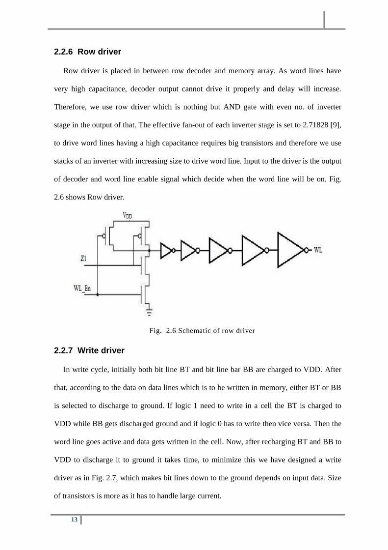
2.2.6 Row driver
Row driver is placed in between row decoder and memory array. As word lines have
very high capacitance, decoder output cannot drive it properly and delay will increase.
Therefore, we use row driver which is nothing but AND gate with even no. of inverter
stage in the output of that. The effective fan-out of each inverter stage is set to 2.71828 [9],
to drive word lines having a high capacitance requires big transistors and therefore we use
stacks of an inverter with increasing size to drive word line. Input to the driver is the output
of decoder and word line enable signal which decide when the word line will be on. Fig.
2.6 shows Row driver.
Fig. 2.6 Schematic of row driver
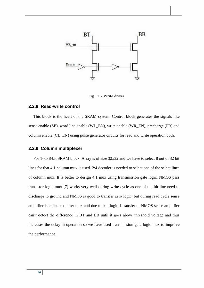
2.2.7 Write driver
In write cycle, initially both bit line BT and bit line bar BB are charged to VDD. After
that, according to the data on data lines which is to be written in memory, either BT or BB
is selected to discharge to ground. If logic 1 need to write in a cell the BT is charged to
VDD while BB gets discharged ground and if logic 0 has to write then vice versa. Then the
word line goes active and data gets written in the cell. Now, after recharging BT and BB to
VDD to discharge it to ground it takes time, to minimize this we have designed a write
driver as in Fig. 2.7, which makes bit lines down to the ground depends on input data. Size
of transistors is more as it has to handle large current.
14
Fig. 2.7 Write driver
2.2.8 Read-write control
This block is the heart of the SRAM system. Control block generates the signals like
sense enable (SE), word line enable (WL_EN), write enable (WR_EN), precharge (PR) and
column enable (CL_EN) using pulse generator circuits for read and write operation both.
2.2.9 Column multiplexer
For 1-kb 8-bit SRAM block, Array is of size 32x32 and we have to select 8 out of 32 bit
lines for that 4:1 column mux is used. 2:4 decoder is needed to select one of the select lines
of column mux. It is better to design 4:1 mux using transmission gate logic. NMOS pass
transistor logic mux [7] works very well during write cycle as one of the bit line need to
discharge to ground and NMOS is good to transfer zero logic, but during read cycle sense
amplifier is connected after mux and due to bad logic 1 transfer of NMOS sense amplifier
can’t detect the difference in BT and BB until it goes above threshold voltage and thus
increases the delay in operation so we have used transmission gate logic mux to improve
the performance.

15
3
SRAM CELL DESIGN
16
As we have discussed in the previous chapter, Orientation of cells in cell array is very
important to achieve frequency specifications, in the same way proper design of SRAM
cell is very important to perform read and write operation. If a SRAM cell is not properly
sized it will lead to destruction of data during the read cycle and also to inappropriate
writing. This chapter describes in details the design of the 6T SRAM cell.
Memory cell needs to be very quick to read and write the single bit to it. The decrease in
supply voltage (VDD) affects the stability of cell [1]. For.25u technology the cell ratio CR
and pull up ratio PR are standard that is for a stable operation, CR need to be in the range
1.5-2 and PR need to be less than 1.8 [17]. In 90nm technology cell ratio and pull up ratio
varies to get required performance. As we go for high frequency the memory cell needs to
be very stable.
In comparison with four transistor resistive load cell, a 6T SRAM cell has greater
immunity to voltage variation and transient noise and lower power consumption in standby
mode. It is the reason why for high speed at low power applications six transistor CMOS
SRAM cell, i.e. 6T is favored over four transistor resistive load cell.
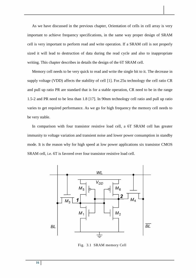
Fig. 3.1 SRAM memory Cell
17
From Fig. 2.1, M1 and M2 are the pull down transistors, M3 and M4 are access transistors
and M5 and M6 are pull up transistors.
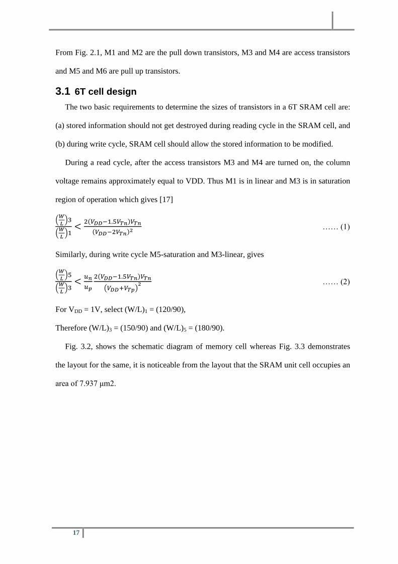
3.1 6T cell design
The two basic requirements to determine the sizes of transistors in a 6T SRAM cell are:
(a) stored information should not get destroyed during reading cycle in the SRAM cell, and
(b) during write cycle, SRAM cell should allow the stored information to be modified.
During a read cycle, after the access transistors M3 and M4 are turned on, the column
voltage remains approximately equal to VDD. Thus M1 is in linear and M3 is in saturation
region of operation which gives [17]
(
)
(
) ( )
( )
…… (1)
Similarly, during write cycle M5-saturation and M3-linear, gives
(
)
(
)
( )
( ) …… (2)
For VDD = 1V, select (W/L)1 = (120/90),
Therefore (W/L)3 = (150/90) and (W/L)5 = (180/90).
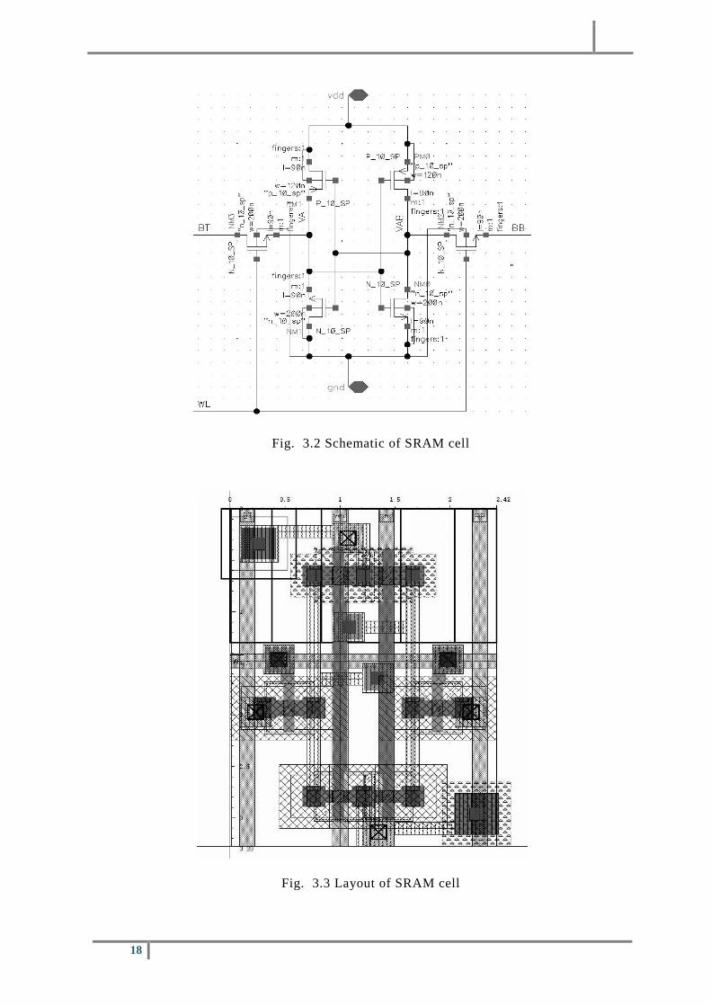
Fig. 3.2, shows the schematic diagram of memory cell whereas Fig. 3.3 demonstrates
the layout for the same, it is noticeable from the layout that the SRAM unit cell occupies an
area of 7.937 μm2.
18
Fig. 3.2 Schematic of SRAM cell
Fig. 3.3 Layout of SRAM cell
19
3.2 Reading and Writing in Cell
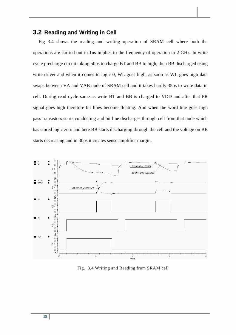
Fig 3.4 shows the reading and writing operation of SRAM cell where both the
operations are carried out in 1ns implies to the frequency of operation to 2 GHz. In write
cycle precharge circuit taking 50ps to charge BT and BB to high, then BB discharged using
write driver and when it comes to logic 0, WL goes high, as soon as WL goes high data
swaps between VA and VAB node of SRAM cell and it takes hardly 35ps to write data in
cell. During read cycle same as write BT and BB is charged to VDD and after that PR
signal goes high therefore bit lines become floating. And when the word line goes high
pass transistors starts conducting and bit line discharges through cell from that node which
has stored logic zero and here BB starts discharging through the cell and the voltage on BB
starts decreasing and in 30ps it creates sense amplifier margin.
Fig. 3.4 Writing and Reading from SRAM cell
20
3.3 Static Noise Margin (SNM)
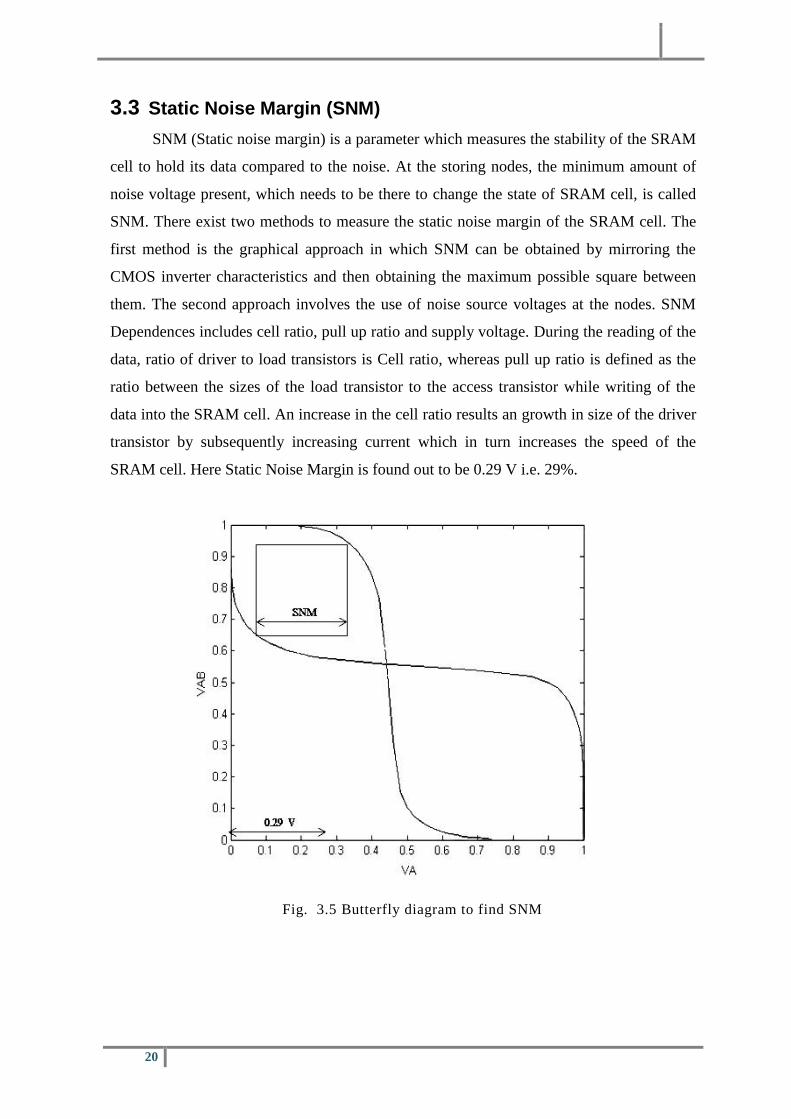
SNM (Static noise margin) is a parameter which measures the stability of the SRAM
cell to hold its data compared to the noise. At the storing nodes, the minimum amount of
noise voltage present, which needs to be there to change the state of SRAM cell, is called
SNM. There exist two methods to measure the static noise margin of the SRAM cell. The
first method is the graphical approach in which SNM can be obtained by mirroring the
CMOS inverter characteristics and then obtaining the maximum possible square between
them. The second approach involves the use of noise source voltages at the nodes. SNM
Dependences includes cell ratio, pull up ratio and supply voltage. During the reading of the
data, ratio of driver to load transistors is Cell ratio, whereas pull up ratio is defined as the
ratio between the sizes of the load transistor to the access transistor while writing of the
data into the SRAM cell. An increase in the cell ratio results an growth in size of the driver
transistor by subsequently increasing current which in turn increases the speed of the
SRAM cell. Here Static Noise Margin is found out to be 0.29 V i.e. 29%.
Fig. 3.5 Butterfly diagram to find SNM
21
4
CELL ARRAY MODELING
22
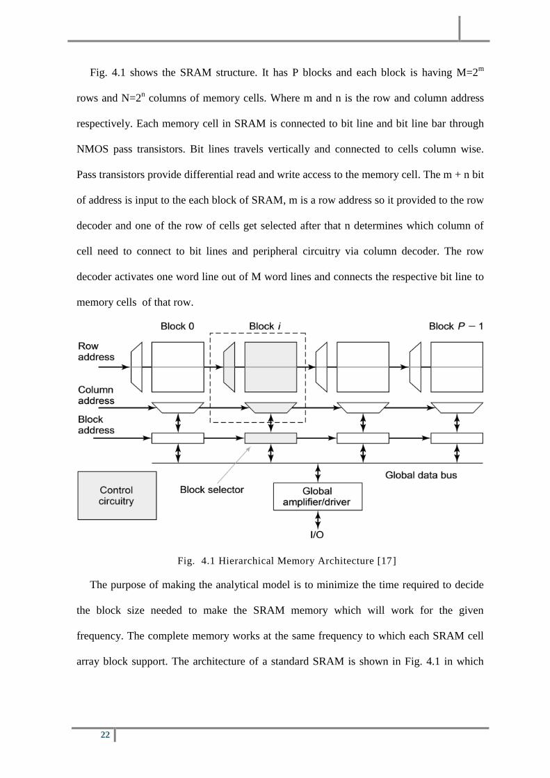
Fig. 4.1 shows the SRAM structure. It has P blocks and each block is having M=2m
rows and N=2n columns of memory cells. Where m and n is the row and column address
respectively. Each memory cell in SRAM is connected to bit line and bit line bar through
NMOS pass transistors. Bit lines travels vertically and connected to cells column wise.
Pass transistors provide differential read and write access to the memory cell. The m + n bit
of address is input to the each block of SRAM, m is a row address so it provided to the row
decoder and one of the row of cells get selected after that n determines which column of
cell need to connect to bit lines and peripheral circuitry via column decoder. The row
decoder activates one word line out of M word lines and connects the respective bit line to
memory cells of that row.
Fig. 4.1 Hierarchical Memory Architecture [17]
The purpose of making the analytical model is to minimize the time required to decide
the block size needed to make the SRAM memory which will work for the given
frequency. The complete memory works at the same frequency to which each SRAM cell
array block support. The architecture of a standard SRAM is shown in Fig. 4.1 in which
23
complete memory is divided into P blocks. If the given frequency of operation of SRAM is
F for which we need to design a memory block. Then total time available is T=1/F.
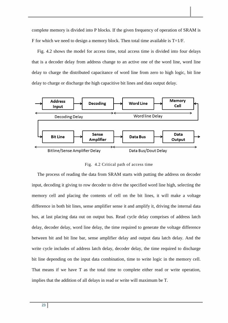
Fig. 4.2 shows the model for access time, total access time is divided into four delays
that is a decoder delay from address change to an active one of the word line, word line
delay to charge the distributed capacitance of word line from zero to high logic, bit line
delay to charge or discharge the high capacitive bit lines and data output delay.
Fig. 4.2 Critical path of access time
The process of reading the data from SRAM starts with putting the address on decoder
input, decoding it giving to row decoder to drive the specified word line high, selecting the
memory cell and placing the contents of cell on the bit lines, it will make a voltage
difference in both bit lines, sense amplifier sense it and amplify it, driving the internal data
bus, at last placing data out on output bus. Read cycle delay comprises of address latch
delay, decoder delay, word line delay, the time required to generate the voltage difference
between bit and bit line bar, sense amplifier delay and output data latch delay. And the
write cycle includes of address latch delay, decoder delay, the time required to discharge
bit line depending on the input data combination, time to write logic in the memory cell.
That means if we have T as the total time to complete either read or write operation,
implies that the addition of all delays in read or write will maximum be T.
24
With change in memory array architecture the effectively affecting delays are word line
delay (TWL), bit line and bit line bar difference time (TBT-BB) and time required to discharge
one of the bitline (TBLdata). Whereas the delay due to decoder, sense amplifier is constant
with their optimize architecture.
If we have to decide the no. of row (N) and no. of columns (M) of the memory array for
specified frequency when peripherals delay is assumed to be constant, then we need to
model the array delays in terms of N and M. The proposed model is based on dynamic
strategies for word line charging, bit line discharging and will not consider the delay as
50% of input to 50% of output, It will check whether device is turned on or not, and the
delay to switch on the device either NMOS or PMOS.
RWL, CWL, RBT and CBT are resistance and capacitance of word line and bit line extracted
from the single memory cell layout. Therefore, here only by drawing the layout for single
cell we can predict the architecture for memory array where same cell will be used.
Word line delay (TWL) can be represented as
(
) …… (3)
By Elmore Delay Formula
( )
…… (4)
Vtnpass is the threshold voltage of the pass transistor in SRAM cell, ∆V is the sense
amplifier margin, that is when ∆V voltage difference is created between BT and BB sense
amplifier will get sense enable signal so that it will amplify the difference and give output
to output data latch. Time to generate BT-BB difference is demonstrated as
(
) …… (5)
By Elmore Delay Formula
25
( ) ( )
…… (6)
RONpass and RONpd is on resistance of pass transistor and pull down transistor of cell from
which data reading operation is carried out. Time to make data available on bit lines during
write cycle is nothing but the time required to discharge one of the bit lines through write
driver
…… (7)
By Elmore Delay Formula
( ) ( )
…… (8)
Here RON is the NMOS on resistance which is present in write driver circuitry. Thus, by
using these equations we can find delay due to word line and bit lines.
F is the frequency on which SRAM supposed to work, then T = 1/F is the total time that
any read or write operation is having to complete their task, as we have assumed that
peripheral circuitry has fixed delay, then array size can be decided by time remains by
subtracting peripheral delay from total time, the remaining time need to be divided into
word line delay and bit line delay, therefore the size of the array will be MxN. The value of
the RBL and CBL is very small compared to RON of pass and pull down transistor, therefore,
from equation 5 and 6, for memory block with less no. of rows bit line delay increases
almost linearly with N, whereas when N increased above a certain value for which second
term in equation 6 becomes effective, the increase in N will increases delay in square law,
it is one of the reason why memory blocks have small sizes to achieve high frequency.
M can be found out by
√
(
) …… (9)
26
And N by using formulas
√ {( )
(
)} …… (10)
√
( ) …… (11)
M can be found out directly by using equation (9) but for N we have to calculate by using
equation (10) and (11) and consider smaller one.
Simulation Results:
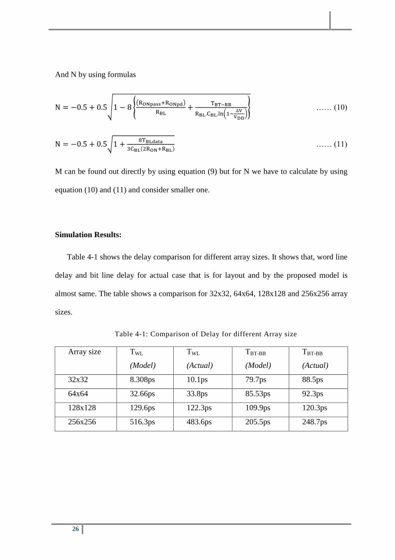
Table 4-1 shows the delay comparison for different array sizes. It shows that, word line
delay and bit line delay for actual case that is for layout and by the proposed model is
almost same. The table shows a comparison for 32x32, 64x64, 128x128 and 256x256 array
sizes.
Table 4-1: Comparison of Delay for different Array size
Array size TWL
(Model)
TWL
(Actual)
TBT-BB
(Model)
TBT-BB
(Actual)
32x32 8.308ps 10.1ps 79.7ps 88.5ps
64x64 32.66ps 33.8ps 85.53ps 92.3ps
128x128 129.6ps 122.3ps 109.9ps 120.3ps
256x256 516.3ps 483.6ps 205.5ps 248.7ps
27
5
HIGH SPEED SENSE AMPLIFIER
28
The sense amplifier (SA) is one of the most important blocks in SRAM memory.
Although various types of SAs are developed, the latch type SA is known for its low power
consumption and high sensing speed [14]. In high performance VLSI circuits the low
power sense amplifiers are required because the huge percentage of total power
consumption is done by on chip memories and interface circuits [10] [12]. To respond high
frequency, the SRAM peripheral circuit needs to be very fast, high speed sense amplifier is
to achieve a significant high speed SRAM memory [11]. Comparative Study of Various
Latch Type Sense Amplifiers [13] gives a comparison in voltage mode and current mode
sense amplifiers also.
Sense amplifier (SA) is an important component in memory design. Read speed,
power and robustness of bit line sensing is defined by the design and choice of sense
amplifier. The function of sense amplifier in SRAM is to sense the small differential
voltage generated on bit line and bit line bar by the memory cell and amplify it to digital
output which leads to reduction in time requirement for read operation. Thus, each memory
cell does not discharge the bit line individually, and hence sense amplifier allows the
memory cell to be small. The minimal bit line differential which is input to SA is called as
SA margin, is a parameter in describing the total read access time and therefore the speed
of an SRAM. Extra read access time and the power needed to spend on the discharging and
precharging of the bit lines for the better tolerance to the process and environmental
fluctuations.
5.1 Current-controlled latch sense amplifier
In high speed VLSI circuits and battery backed up systems, power dissipation is a
serious limitation. In proportion to the speed of operation, power dissipation of high speed
circuits increases. The on chip memories and interface circuits dissipates larger percentage
of total power this is the reason why low power sense amplifiers and interface circuits are
29
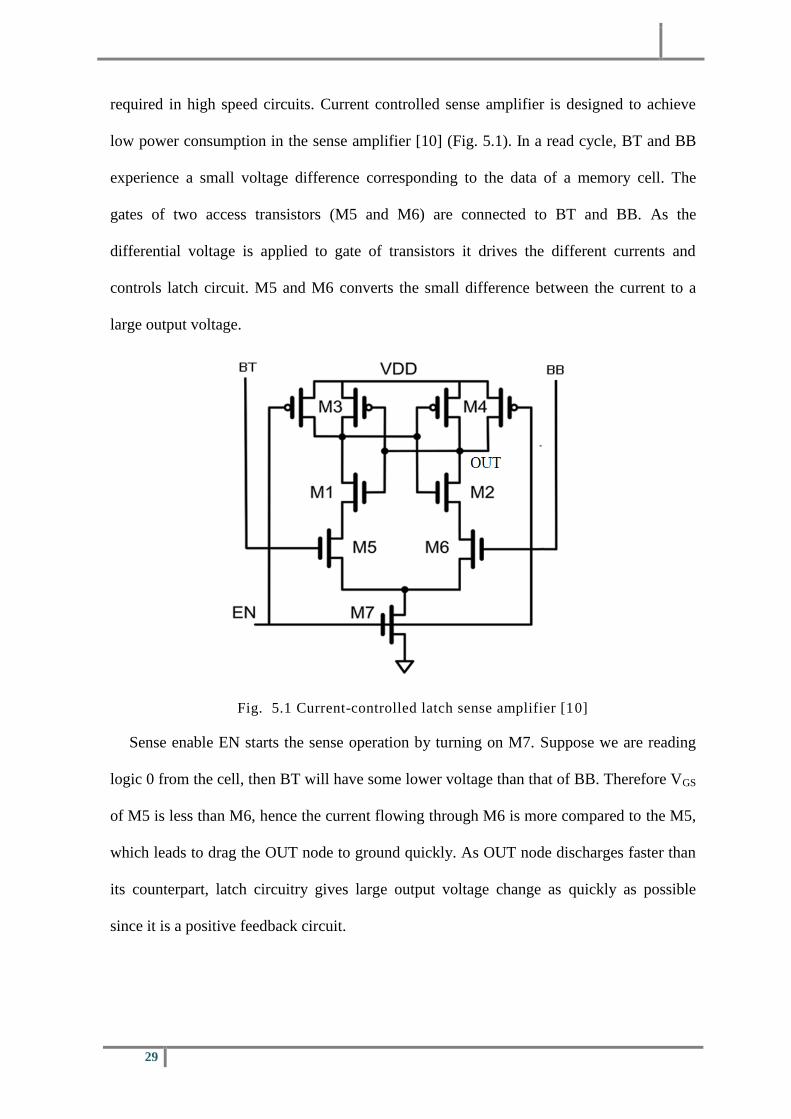
required in high speed circuits. Current controlled sense amplifier is designed to achieve
low power consumption in the sense amplifier [10] (Fig. 5.1). In a read cycle, BT and BB
experience a small voltage difference corresponding to the data of a memory cell. The
gates of two access transistors (M5 and M6) are connected to BT and BB. As the
differential voltage is applied to gate of transistors it drives the different currents and
controls latch circuit. M5 and M6 converts the small difference between the current to a
large output voltage.
Fig. 5.1 Current-controlled latch sense amplifier [10]
Sense enable EN starts the sense operation by turning on M7. Suppose we are reading
logic 0 from the cell, then BT will have some lower voltage than that of BB. Therefore VGS
of M5 is less than M6, hence the current flowing through M6 is more compared to the M5,
which leads to drag the OUT node to ground quickly. As OUT node discharges faster than
its counterpart, latch circuitry gives large output voltage change as quickly as possible
since it is a positive feedback circuit.
30
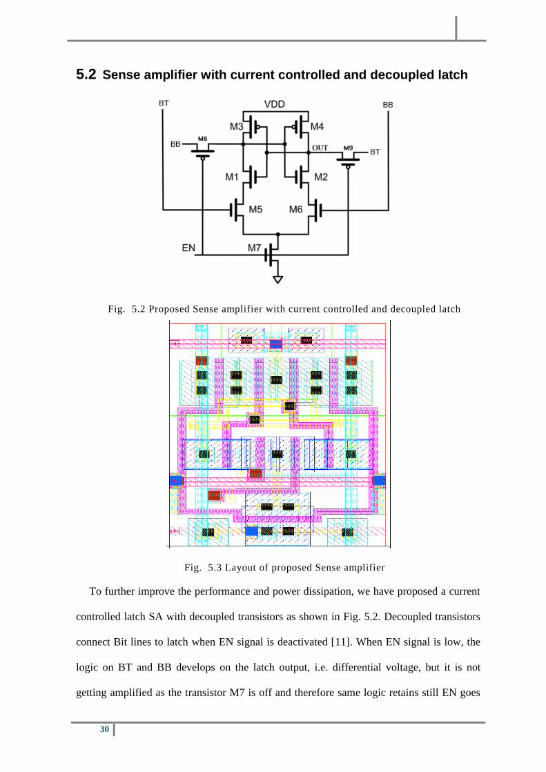
5.2 Sense amplifier with current controlled and decoupled latch
Fig. 5.2 Proposed Sense amplifier with current controlled and decoupled latch
Fig. 5.3 Layout of proposed Sense amplifier
To further improve the performance and power dissipation, we have proposed a current
controlled latch SA with decoupled transistors as shown in Fig. 5.2. Decoupled transistors
connect Bit lines to latch when EN signal is deactivated [11]. When EN signal is low, the
logic on BT and BB develops on the latch output, i.e. differential voltage, but it is not
getting amplified as the transistor M7 is off and therefore same logic retains still EN goes
31
high. Here line having low voltage goes to discharge to ground when EN signal goes high.
When EN signal is highly decoupled transistors disconnect the BT and BB signals from
latch circuit and it act as a current controlled latch as in [10]. Low voltage path is going to
discharge after EN goes high therefore it is quicker than current controlled SA to give
output and is having less power dissipation. The comparative study of proposed with
current controlled latch SA [10] and CMOS current sense amplifier [15] shows the
performance and power dissipation improvement of proposed over them.
5.3 Simulation Results and Discussions
5.3.1 Power and Delay Comparison
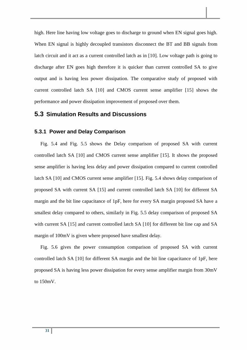
Fig. 5.4 and Fig. 5.5 shows the Delay comparison of proposed SA with current
controlled latch SA [10] and CMOS current sense amplifier [15]. It shows the proposed
sense amplifier is having less delay and power dissipation compared to current controlled
latch SA [10] and CMOS current sense amplifier [15]. Fig. 5.4 shows delay comparison of
proposed SA with current SA [15] and current controlled latch SA [10] for different SA
margin and the bit line capacitance of 1pF, here for every SA margin proposed SA have a
smallest delay compared to others, similarly in Fig. 5.5 delay comparison of proposed SA
with current SA [15] and current controlled latch SA [10] for different bit line cap and SA
margin of 100mV is given where proposed have smallest delay.
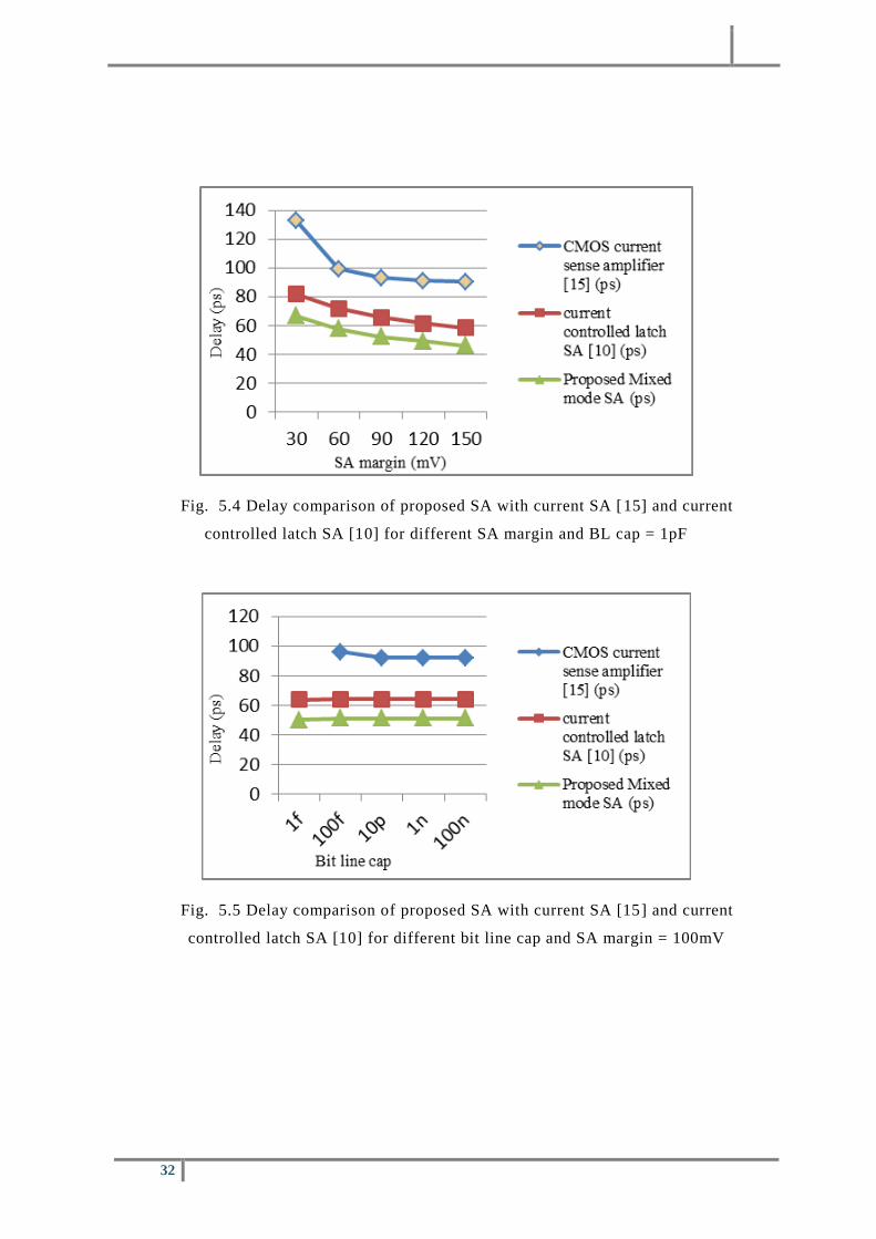
Fig. 5.6 gives the power consumption comparison of proposed SA with current
controlled latch SA [10] for different SA margin and the bit line capacitance of 1pF, here
proposed SA is having less power dissipation for every sense amplifier margin from 30mV
to 150mV.
32
Fig. 5.4 Delay comparison of proposed SA with current SA [15] and current
controlled latch SA [10] for different SA margin and BL cap = 1pF
Fig. 5.5 Delay comparison of proposed SA with current SA [15] and current
controlled latch SA [10] for different bit line cap and SA margin = 100mV
33
Fig. 5.6 Power consumption comparison of proposed SA with current controlled latch
SA [10] for different SA margin and BL cap = 1pF
5.3.2 Corner Analysis
Table I gives the results for corner analysis where the largest delay is found out for SS
case and it is 75.81ps whereas the smallest is for FF case and it is 38.06ps.
Table 5-1: CORNER ANALYSIS
Delay (ps)
NN 51.08
SS 75.81
SF 73.71
FS 38.70
FF 38.06
34
5.3.3 Monte Carlo Analysis
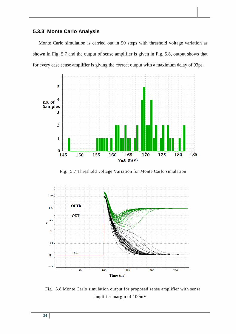
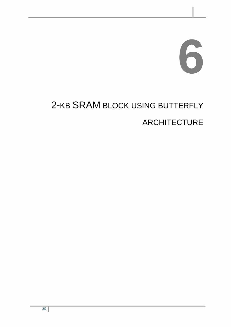
Monte Carlo simulation is carried out in 50 steps with threshold voltage variation as
shown in Fig. 5.7 and the output of sense amplifier is given in Fig. 5.8, output shows that
for every case sense amplifier is giving the correct output with a maximum delay of 93ps.
Fig. 5.7 Threshold voltage Variation for Monte Carlo simulation
Fig. 5.8 Monte Carlo simulation output for proposed sense amplifier with sense
amplifier margin of 100mV
35
6
2-KB SRAM BLOCK USING BUTTERFLY
ARCHITECTURE
36
As described in chapter 4, to reduce the bit line capacitance and bit line leakage, we
divide taller memories and try to make it wider and maintain aspect ratio. But in wide
memories, word line RC is problematic, and therefore we use Butterfly architecture, i.e.
central decoding to overcome this problem. Butterfly architecture is described in section
6.1 of this chapter, whereas design of 2 kb SRAM using the same architecture and its
internal blocks is explained in the next section.
6.1 Butterfly Architecture (central decoding)
Fig. 6.1 Butterfly Architecture for SRAM
To increase the speed for SRAM, we try to minimize the bit line capacitance. To
minimize the bit line capacitance, we try to make SRAM array as wide as possible. When
we make array wider, word line takes more time to propagate signals up to last cell in a
row because increased RC delay in the path. From eqn. 4 in chapter 4, word line delay is
directly proportional to per unit resistance and capacitance of word line, as length is
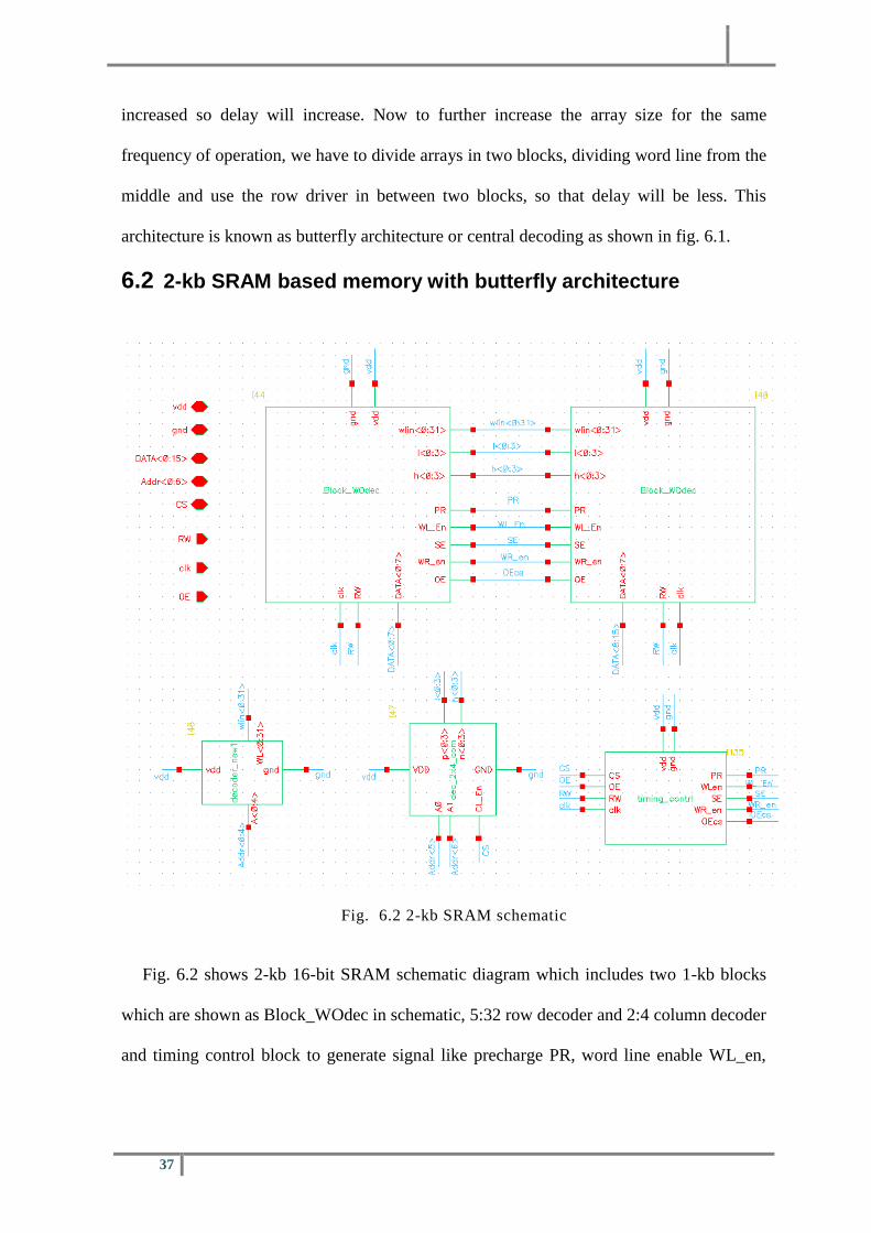
37
increased so delay will increase. Now to further increase the array size for the same
frequency of operation, we have to divide arrays in two blocks, dividing word line from the
middle and use the row driver in between two blocks, so that delay will be less. This
architecture is known as butterfly architecture or central decoding as shown in fig. 6.1.
6.2 2-kb SRAM based memory with butterfly architecture
Fig. 6.2 2-kb SRAM schematic
Fig. 6.2 shows 2-kb 16-bit SRAM schematic diagram which includes two 1-kb blocks
which are shown as Block_WOdec in schematic, 5:32 row decoder and 2:4 column decoder
and timing control block to generate signal like precharge PR, word line enable WL_en,
38
sense enable SE, write enable WR_en and output enable for chip OEcs from input signals
chip select CS, output enable OE, clock clk and read write bar RW.
Here 2-kb 16-bit SRAM block is designed using 1-kb 8-bit SRAM block, decoder and
timing control circuit. The timing control block uses pulse generating circuitry to generate
signals and static decoder is used make address decoder for 2-kb SRAM. Two 1-kb 8-bit
SRAM blocks are used in parallel to make 2-kb 16-bit SRAM block, therefore the
frequency of operation for 2-kb is same as that of 1-kb SRAM block. At a time both 1-kb
blocks are accessed to read or write to 8 bits of each block. A design of 1-kb block is
described in the next section which does not contain decoder and timing block.
2-kb SRAM has total 29 pins that are CS, RW, clk, OE, Address<0:6>, Data<0:15> and
two power supply pins. When chip select CS is high, corresponding 2-kb block get selected
and when CS is on then only control signals are generated for that block otherwise not.
Read write input signal tells the next cycle will be read or write, 1 for read and 0 for write.
Clk is clock signal and all internal signals to get generated with respect to clk, as it is a
synchronous SRAM. OE is the output enable signal, at the end of read cycle this signal
goes high to get output from 1 bit latch through the buffer. The address is 7 bits while data
are 16 bits as it is 2-kb 16-bit memory block.
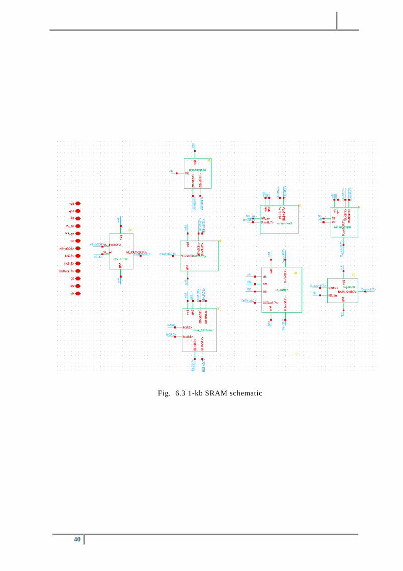
6.3 1-kb SRAM design
1-kb SRAM block which is used for butterfly architecture in 2-kb SRAM contain blocks
like precharge, row driver, cell array, column mux, sense amplifier, write driver, data latch
and IO buffer. Complete schematic of 1-kb SRAM is shown in fig. 6.3.
For 1-kb SRAM the memory array should have an aspect ratio as 128x8. It is not
practically good to go with such aspect ratio and also bit line capacitance increases with
increase in bit line length. So we have divided the 128 rows into 4 portions and used a 4:1
Mux to select one out of these. Now the memory array is perfectly square that is aspect
39
ratio of 32x32. We have used memory cell designed in chapter 3 for the memory cell array.
The sense amplifier plays an important role in the functionality, performance and reliability
of the memory circuits. We have used high speed current controlled and decoupled latch
sense amplifier which is discussed in chapter 6. Precharge circuit is used to charge both bit
lines to VDD. It is to be performed before every read and write operation. As bit lines have
high capacitance, precharge circuit needs to provide large current to bit lines to get charged
quickly. Therefore the size of transistors used in precharge circuit is large. Fig. 6.5 (a)
shows precharge schematic and fig. 6.5 (b) shows instances created, for 32 bit lines. Row
driver is placed in between row decoder and memory array. As word lines have very high
capacitance, decoder output cannot drive it properly and delay will increase. Therefore, we
use row driver which is nothing but AND gate with even no. of inverter stage in the output
of that. Input to the driver is the output of decoder and word line enable signal which
decide when the word line will be on. Fig. 6.7 shows Row driver schematic and 32
instances for 32 word lines. In write cycle, initially both bit line BT and bit line bar BB are
charged to VDD. After that, according to the data on data lines which is to be written in
memory, either BT or BB is selected to discharge to ground. If logic 1 need to write in a
cell the BT is charged to VDD while BB gets discharged ground and if logic 0 has to write
then vice versa. Then the word line goes active and data gets written in the cell. Now, after
precharging BT and BB to VDD to discharge it to ground it takes time, to minimize this we
have designed a write driver as in Fig. 6.6, which makes bit lines down to the ground
depends on input data. For 1-kb 8-bit SRAM block, Array is of size 32x32 and we have to
select 8 out of 32 bit lines for that 4:1 column mux is used.
40
Fig. 6.3 1-kb SRAM schematic
41
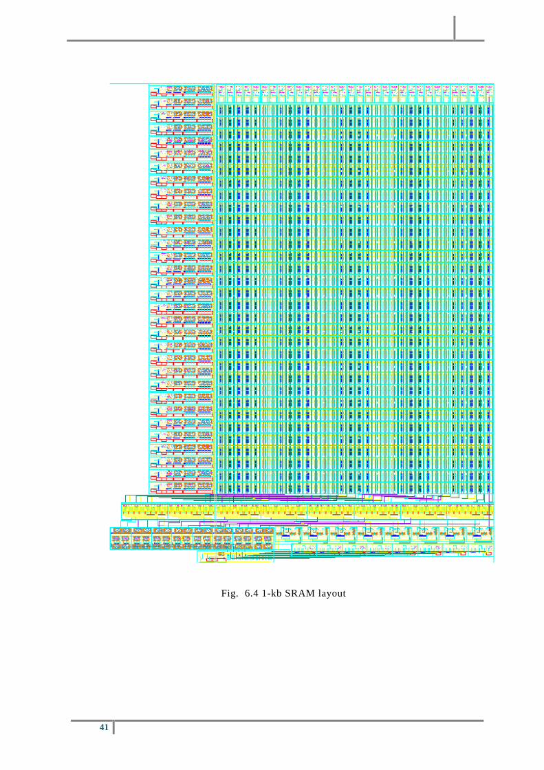
Fig. 6.4 1-kb SRAM layout
42
(a)
(b)
Fig. 6.5 precharge (a) schematic, (b) 32 instances for 32 columns
43
(a)
(b)
Fig. 6.6 Write driver (a) schematic, (b) 8 instances for 8 bit data
44
(a)
(b)
Fig. 6.7 Row driver (a) schematic, (b) 32 instances for 32 rows
45
6.4 Simulation Results and Discussions
2-kb SRAM using butterfly architecture is designed and layout is drawn for the same
using UMC 90nm technology in Cadence. Complete memory is simulated and read and
write operation is checked for the same. Fig. 6.8 shows the test bench for 2-kb SRAM,
where RW, clk, CS, OE and address is the input to the memory with data lines as input-
output. During read cycle RW is logic 1 and data lines are floating whereas during write
cycle RW is logic 0 and data input id given on data lines which is to be written in memory.
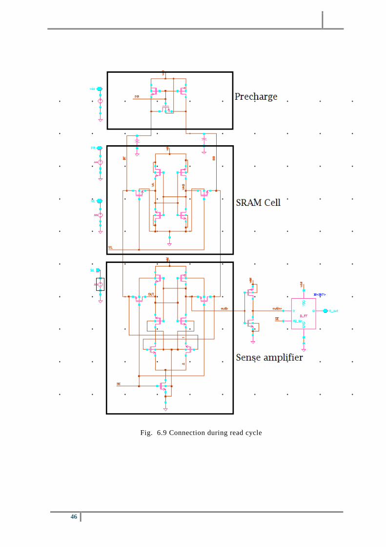
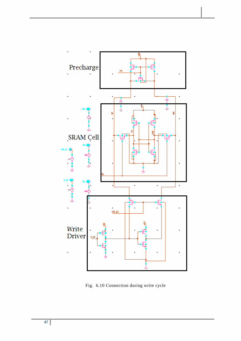
During a read cycle we can see connection in memory as shown in fig. 6.9 and fig. 6.10
shows the equivalent circuit during a write cycle.
Fig. 6.8 2-kb SRAM test bench
46
Fig. 6.9 Connection during read cycle
47
Fig. 6.10 Connection during write cycle
48
6.4.1 Read and write cycle for 2-kb SRAM
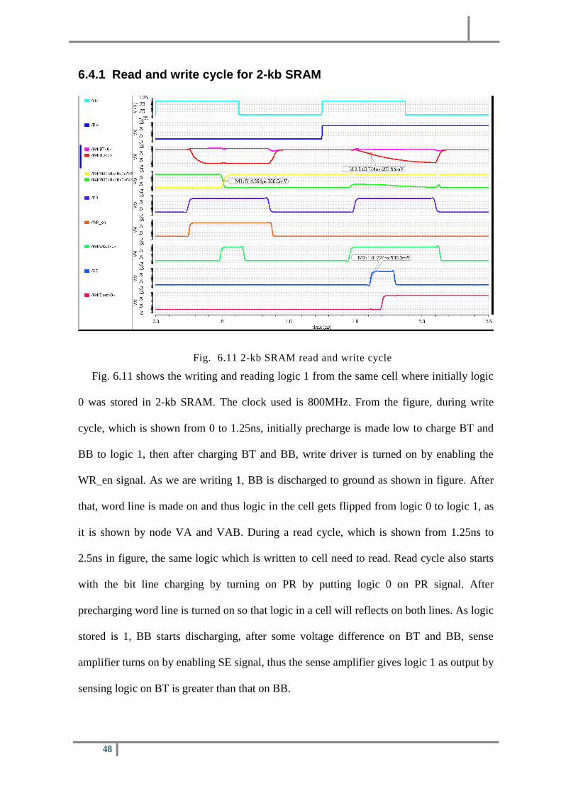
Fig. 6.11 2-kb SRAM read and write cycle
Fig. 6.11 shows the writing and reading logic 1 from the same cell where initially logic
0 was stored in 2-kb SRAM. The clock used is 800MHz. From the figure, during write
cycle, which is shown from 0 to 1.25ns, initially precharge is made low to charge BT and
BB to logic 1, then after charging BT and BB, write driver is turned on by enabling the
WR_en signal. As we are writing 1, BB is discharged to ground as shown in figure. After
that, word line is made on and thus logic in the cell gets flipped from logic 0 to logic 1, as
it is shown by node VA and VAB. During a read cycle, which is shown from 1.25ns to
2.5ns in figure, the same logic which is written to cell need to read. Read cycle also starts
with the bit line charging by turning on PR by putting logic 0 on PR signal. After
precharging word line is turned on so that logic in a cell will reflects on both lines. As logic
stored is 1, BB starts discharging, after some voltage difference on BT and BB, sense
amplifier turns on by enabling SE signal, thus the sense amplifier gives logic 1 as output by
sensing logic on BT is greater than that on BB.
49
6.4.2 Process Corner Analysis
In the manufacturing process, a process corner analysis is a technique that refers to a
variation of fabrication parameters. Process corners represent the extremes of these
parameter variations. At different temperatures and voltage, the NMOS and PMOS will be
either slow or fast and therefore the corners are defined as typical-typical (TT), Fast-Fast
(FF) and Slow-Slow (SS), here first case is of NMOS and second for PMOS. If the circuit
fails to work at any corner, then it is the bad design to be considered for manufacturing.
We have checked the all process variation corners for 2-kb SRAM, and detailed results
and timing are given in table 6.1 for all the five cases. We are checking the effect of
process parameters on delay in write logic change point (write sweep point), time to
develop sense amplifier margin (SA margin delay), time to discharge bit line (bit line
delay) and data out delay. For all the corners, 2-kb SRAM is performing proper reading
and writing operation with the maximum speed 800MHz.
Table 6-1: Delay for different corners of 2-kb SRAM
Corners Write sweep
point
SA margin SA
margin
delay
Bit line
delay
Data out
delay
Typical-Typical
(TT)
514 ps 308 mV 117 ps 146 ps 93 ps
Fast-fast
(FF)
428 ps 328 mV 58 ps 89 ps 66 ps
Slow-slow
(SS)
655 ps 288 mV 212 ps 180 ps 109 ps
Slow n -FAST p
(SNFP)
526 ps 378 mV 122 ps 81 ps 98 ps
Fast n-Slow p
(FNSP)
510 ps 373 mV 115 ps 130 ps 92 ps
50
7
CONCLUSION
51
Static random access memory (SRAM) is designed with its peripheral blocks to achieve
operation of frequency 800 MHz, with memory cell having static noise margin of 29%.
Analytical model to predict the block size for memory is developed. Analytical models for
delay permit one to explore a range of design possibilities in a very short span of time. This
model is used to study the impact of SRAM partitioning. For memory block with less no.
of rows, bit line delay increases almost linearly with increase in row numbers, whereas for
large no. of rows, the increase in row number will increases delay in square law, it is one of
the reason why memory blocks have small sizes to achieve high frequency. A sense
amplifier with decoupled latch and current controlled logic is designed. As the voltage
available and need be discharged to ground is less than supply voltage, it is having
improvement over current controlled latch sense amplifier in terms of power dissipation
and performance. Butterfly architecture is used to design 2-kb using 1-kb SRAM block
which works on the operation frequency of 800MHz. Thus 2-kb 16-bit, 800MHz SRAM is
designed and layout drawn for the same and checked for reading and writing operation also
corner analysis is done to check the all PVT variations affects, and it is working at
800MHz for worst case scenario also.
The future works that can be conducted for manufacturing of 1MB chip using designed
2-kb block. For that 1MB memory need to design and draw a layout of the same using 2-kb
block so that operating frequency will be near to 800MHz. All the post layout checks need
to be done like antenna effect, EM check, electrostatic discharge, IR drop and need to
check the reliability issues.
52
DISSEMINATION
R. D. Chandankhede, D. P. Acharya, P. K. Patra, “Design of High Speed Sense Amplifier
for SRAM”, IEEE International Conference on Advanced Communication Control and
Computing Technologies 2014, pp. 340-343, May 2014.
53
REFERENCES
[1] E. Grossar, M. Stucchi, K. Maex and W. Dehaene, “Read Stability and Write-Stability
Analysis of SRAM Cells for Nanometer Technologies,” IEEE J. Solid State Circuits, vol. 41,
no. 11, pp. 2577-2588, Nov. 2006.
[2] T. Wada, S. Rajan, and S. Przybylski, “An analytical access time model for on-chip cache
memories,” IEEE J. Solid State Circuits, vol. 27, no. 8, pp. 1147–1156, Aug. 1992.
[3] S. Wilton and N. jouppi, “CACTI: An Enhanced cache access and cycle time model,” IEEE J.
Solid-State Circuits, vol. 31, no. 5, pp. 175–185, May 1996.
[4] B. Amrutur and M. Horowitz, “Speed and power scaling of SRAM’s,” IEEE J. Solid-State
Circuits, vol. 35, no. 2, pp. 175–185, Feb. 2000.
[5] A. Zeng, K. Rose and R. Gutmann, “Memory Performance Prediction for High-Performance
Microprocessors at Deep Submicrometer Technologies,” IEEE Trans. on CAD of ICs and
system, vol. 25, no. 9, pp. 1705–1718, Sep. 2006.
[6] K. Zhang, F. Hamzaoglu and Y. Wang, “Low-Power SRAMs in Nanoscale CMOS
Technologies,” IEEE Trans. On Electron Devices, vol. 55, no. 1, pp. 145–151, Jan. 2008.
[7] W. Kenneth, M. Toshihiko, B. Amrutur, Ron Ho, B. Wilburn, M. Horowitz, I. Fukushi, T.
Izawa and S. Mitarai, “Low-Power SRAM Design Using Half-Swing Pulse-
ModeTechniques,” IEEE J. Solid-State Circuits, vol.33, no.11, pp.1659–1671,Nov. 1998.
[8] K. Khare, N. Khare, V. Kulhade and P. Deshpande, “VLSI Design And Analysis Of Low
Power 6T SRAM Cell Using Cadence Tool,” leSE, lohor Bahru, Malaysia, 2008.
[9] J. Meindl et al., “The impact of stochastic dopant and interconnect distributions on gigascale
integration,” IEEE Int. Solid-State Circuits Conf., pp. 232–233, 1997
[10] T. Kobayashi, K. Nogami, T. Shirotori, and Y. Fujimoto, “A current controlled latch sense
amplifier and a static power-saving input buffer for low-power architecture,” IEEE J. Solid-
State Circuits, vol. 28, pp. 523-527, 1993.
54
[11] T. Seki, E. Itoh, C. Furukawa, I. Maeno, T. Ozawa, and H. Sano, “A 6-ns 1-Mb CMOS
SRAM with latched sense amplifier,” IEEE J. Solid-State Circuits, vol. 28, pp. 478-483, 1993.
[12] Ya-Chun Lai and Shi-Yu Huang, “A Resilient and Power-Efficient Automatic Power down
Sense Amplifier for SRAM Design,” IEEE Trans. On Circuits & Systems, vol. 55, no. 10, pp.
1031-1035, Oct. 2008.
[13] Taehui Na, S. Woo, J. Kim, H. Jeong, and S. Jung, “Comparative Study of Various Latch-
Type Sense Amplifiers,” IEEE Trans. On VLSI Systems, vol. 22, no. 2, pp. 425-429, Feb.
2014.
[14] B. Wicht, T. Nirschl, and D. Schmitt-Landsiedel, “Yield and speed optimization of a latch-
type voltage sense amplifier,” IEEE J. Solid-State Circuits, vol. 39, no. 7, pp. 1148–1158, Jul.
2004.
[15] Y.K. Seng and S.S. Rofail, “1.5V high speed low power CMOS current sense amplifier,”
ELECTRONICS LETTERS, vol. 31, no. 23, pp. 1991-93, Non. 1995.
[16] Sung-Mo Kang and Yusuf Leblebici, “Cmos Digital Integrated Circuits,” Tata McGraw-
Hill Education, 2003.
[17] Jan M. Rabaey, Anantha Chandrakasan, and Borivoje Nikolic, “Digital Integrated Circuits
a Design Perspective,” PHI Learning, 2009.
[18] “Intel® Core™ i7-920 Processor” [Online].
Available: http://ark.intel.com/products/37147/
[19] “Qualcomm QSD8250 (Snapdragon) 1024 MHz (65 nm)” [Online].
Available: http://www.7-cpu.com/cpu/Snapdragon.html
[20] “The Invention of the Intel 1103 - The World's First Available DRAM Chip By Mary
Bellis” [Online]. Availabe: http://inventors.about.com/library/weekly/aa100898.htm