Embed Size (px)
Citation preview
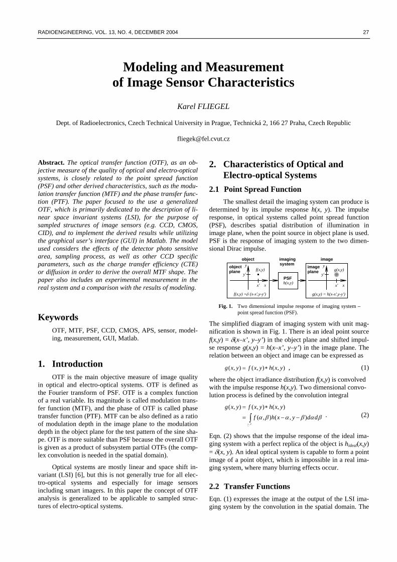
RADIOENGINEERING, VOL. 13, NO. 4, DECEMBER 2004 27
Modeling and Measurement of Image Sensor Characteristics
Karel FLIEGEL
Dept. of Radioelectronics, Czech Technical University in Prague, Technická 2, 166 27 Praha, Czech Republic
Abstract. The optical transfer function (OTF), as an ob-jective measure of the quality of optical and electro-optical systems, is closely related to the point spread function (PSF) and other derived characteristics, such as the modu-lation transfer function (MTF) and the phase transfer func-tion (PTF). The paper focused to the use a generalized OTF, which is primarily dedicated to the description of li-near space invariant systems (LSI), for the purpose of sampled structures of image sensors (e.g. CCD, CMOS, CID), and to implement the derived results while utilizing the graphical user’s interface (GUI) in Matlab. The model used considers the effects of the detector photo sensitive area, sampling process, as well as other CCD specific parameters, such as the charge transfer efficiency (CTE) or diffusion in order to derive the overall MTF shape. The paper also includes an experimental measurement in the real system and a comparison with the results of modeling.
Keywords OTF, MTF, PSF, CCD, CMOS, APS, sensor, model-ing, measurement, GUI, Matlab.
1. Introduction OTF is the main objective measure of image quality
in optical and electro-optical systems. OTF is defined as the Fourier transform of PSF. OTF is a complex function of a real variable. Its magnitude is called modulation trans-fer function (MTF), and the phase of OTF is called phase transfer function (PTF). MTF can be also defined as a ratio of modulation depth in the image plane to the modulation depth in the object plane for the test pattern of the sine sha-pe. OTF is more suitable than PSF because the overall OTF is given as a product of subsystem partial OTFs (the comp-lex convolution is needed in the spatial domain).
Optical systems are mostly linear and space shift in-variant (LSI) [6], but this is not generally true for all elec-tro-optical systems and especially for image sensors including smart imagers. In this paper the concept of OTF analysis is generalized to be applicable to sampled struc-tures of electro-optical systems.
2. Characteristics of Optical and Electro-optical Systems
2.1 Point Spread Function The smallest detail the imaging system can produce is
determined by its impulse response h(x, y). The impulse response, in optical systems called point spread function (PSF), describes spatial distribution of illumination in image plane, when the point source in object plane is used. PSF is the response of imaging system to the two dimen-sional Dirac impulse.
x'
y'
object plane
y
x
f(x,y)
f(x,y) = (x-x',y-y')δ
x'
y'
image plane
y
x
g(x,y)
g(x,y) = h(x-x',y-y')
h(x,y)PSF
object image imagingsystem
Fig. 1. Two dimensional impulse response of imaging system –
point spread function (PSF).
The simplified diagram of imaging system with unit mag-nification is shown in Fig. 1. There is an ideal point source f(x,y) = δ(x–x’, y–y’) in the object plane and shifted impul-se response g(x,y) = h(x–x’, y–y’) in the image plane. The relation between an object and image can be expressed as
( , ) ( , ) ( , )g x y f x y h x y= ∗ , (1)
where the object irradiance distribution f(x,y) is convolved with the impulse response h(x,y). Two dimensional convo-lution process is defined by the convolution integral
2
( , ) ( , ) ( , )
( , ) ( , )
g x y f x y h x y
f h x y d dα β α β α β
= ∗
= − −∫ . (2)
Eqn. (2) shows that the impulse response of the ideal ima-ging system with a perfect replica of the object is hideal(x,y) = δ(x, y). An ideal optical system is capable to form a point image of a point object, which is impossible in a real ima-ging system, where many blurring effects occur.
2.2 Transfer Functions Eqn. (1) expresses the image at the output of the LSI ima-ging system by the convolution in the spatial domain. The
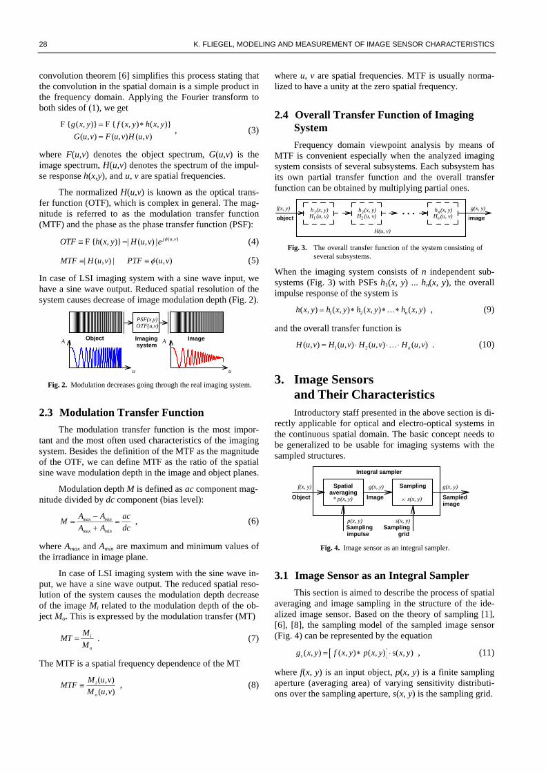
28 K. FLIEGEL, MODELING AND MEASUREMENT OF IMAGE SENSOR CHARACTERISTICS
convolution theorem [6] simplifies this process stating that the convolution in the spatial domain is a simple product in the frequency domain. Applying the Fourier transform to both sides of (1), we get
{ ( , )} { ( , ) ( , )}( , ) ( , ) ( , )
g x y f x y h x yG u v F u v H u v
= ∗=
F F , (3)
where F(u,v) denotes the object spectrum, G(u,v) is the image spectrum, H(u,v) denotes the spectrum of the impul-se response h(x,y), and u, v are spatial frequencies.
The normalized H(u,v) is known as the optical trans-fer function (OTF), which is complex in general. The mag-nitude is referred to as the modulation transfer function (MTF) and the phase as the phase transfer function (PSF):
( , ){ ( , )} | ( , ) | j u vOTF h x y H u v e φ≡ =F (4)
| ( , ) | ( , )MTF H u v PTF u vφ≡ ≡ (5)
In case of LSI imaging system with a sine wave input, we have a sine wave output. Reduced spatial resolution of the system causes decrease of image modulation depth (Fig. 2).
A
u
A
u
ImagingObject Image
PSF(x,y)OTF(u,v)
system
Fig. 2. Modulation decreases going through the real imaging system.
2.3 Modulation Transfer Function The modulation transfer function is the most impor-
tant and the most often used characteristics of the imaging system. Besides the definition of the MTF as the magnitude of the OTF, we can define MTF as the ratio of the spatial sine wave modulation depth in the image and object planes.
Modulation depth M is defined as ac component mag-nitude divided by dc component (bias level):
max min
max min
A A aM cA A d
−= =
+ c , (6)
where Amax and Amin are maximum and minimum values of the irradiance in image plane.
In case of LSI imaging system with the sine wave in-put, we have a sine wave output. The reduced spatial reso-lution of the system causes the modulation depth decrease of the image Mi related to the modulation depth of the ob-ject Mo. This is expressed by the modulation transfer (MT)
i
o
MMTM
= . (7)
The MTF is a spatial frequency dependence of the MT
( , )( , )
i
o
M u vMTFM u v
≡ , (8)
where u, v are spatial frequencies. MTF is usually norma-lized to have a unity at the zero spatial frequency.
2.4 Overall Transfer Function of Imaging System Frequency domain viewpoint analysis by means of
MTF is convenient especially when the analyzed imaging system consists of several subsystems. Each subsystem has its own partial transfer function and the overall transfer function can be obtained by multiplying partial ones.
. . .h (x, y)H (u, v)
11
h (x, y)H (u, v)
22
h (x, y)H (u, v)
nn
H(u, v)
f(x, y)
objectg(x, y)
image
Fig. 3. The overall transfer function of the system consisting of
several subsystems.
When the imaging system consists of n independent sub-systems (Fig. 3) with PSFs h1(x, y) ... hn(x, y), the overall impulse response of the system is
1 2( , ) ( , ) ( , ) ( , )nh x y h x y h x y h x y= ∗ ∗ ∗K , (9)
and the overall transfer function is
1 2( , ) ( , ) ( , ) ( , )nH u v H u v H u v H u v= ⋅ ⋅ ⋅K . (10)
3. Image Sensors and Their Characteristics Introductory staff presented in the above section is di-
rectly applicable for optical and electro-optical systems in the continuous spatial domain. The basic concept needs to be generalized to be usable for imaging systems with the sampled structures.
Spatialaveraging
* p(x, y)
Sampling
Image Sampledimage
Object s(x, y)×
Sampling impulse
Sampling grid
Integral sampler
g(x, y) g(x, y)f(x, y)
s(x, y)p(x, y)
Fig. 4. Image sensor as an integral sampler.
3.1 Image Sensor as an Integral Sampler This section is aimed to describe the process of spatial
averaging and image sampling in the structure of the ide-alized image sensor. Based on the theory of sampling [1], [6], [8], the sampling model of the sampled image sensor (Fig. 4) can be represented by the equation
[ ]( , ) ( , ) ( , ) s( , )sg x y f x y p x y x y= ∗ ⋅ , (11)
where f(x, y) is an input object, p(x, y) is a finite sampling aperture (averaging area) of varying sensitivity distributi-ons over the sampling aperture, s(x, y) is the sampling grid.
RADIOENGINEERING, VOL. 13, NO. 4, DECEMBER 2004 29
The spectrum of the sampled image Gs(u, v) is given by Fourier transform of (11). Recalling the convolution theorem, we can write
[ ]( , ) ( , ) ( , ) ( , )sG u v F u v P u v S u v= ⋅ ∗ , (12)
where F(u, v), P(u, v) and S(u, v) are Fourier images of the functions from (11). S(u, v) is a spectrum of the spatially restricted sampling grid. In case of the ideal sampling (spa-tially non-restricted) and the ideal image restoration
( , ) ( , )S u v u vδ≈ . (13)
Eqn. (12) can be then rewritten to the form
( , ) ( , ) ( , )rG u v F u v P u v= ⋅ , (14)
where Gr(u, v) is a spectrum of the reconstructed image.
Considering (14), OTF of the spatial filtering (spatial averaging on the detector aperture) is obviously
( , )( , ) ( , ) { ( , )}( , )
rdet
G u vOTF u v P u v p x yF u v
≡ = = F . (15)
P(u, v) is Fourier image of sampling impulse p(x, y), and it is called the detector OTF [4] or the footprint OTF [1].
For a detector of a given shape and the uniform sensi-tivity distribution, the function p(x, y) is defined as follows
1 ( , )( , )
0 ( , )p
x y PAp x y
x y P
⎧ ∈⎪= ⎨⎪ ∉⎩
. (16)
Ap is the detector aperture area, (x, y) ∈ P and (x, y) ∉ P mean the position inside and outside the detector, resp.
WS WS
Fig. 5. Wigner-Seitz cell for the rectangular and hexagonal sam-
pling grid. Sampling sites are depicted by black dots.
In a more general case of a non-uniform sensitivity detec-tor aperture, p(x, y) is normalized to meet the condition
( , )
( , ) 1x y P
p x y dxdy∈
=∫∫ . (17)
Considering (15), the detector MTF can be given by
( , ) ( , )det detMTF u v OTF u v= . (18)
3.2 Shift Variance and Sampling MTF Obviously, the sampled imaging system is not inva-
riant to a space shift: position of the source object with respect to the sampling sites affects the final image data. The sampled imaging system has several different MTFs for one spatial frequency depending on the phase between
the sampling grid and the object. One of possible ways of eliminating the space shift dependence from the MTF con-sists in evaluating the average impulse response and the average MTF assuming the scene is randomly positioned with respect to the sampling sites [1], [8]. This MTF is cal-led the sampling MTF or the shift invariant MTF.
An analytic approach can be also used for the samp-ling MTF. Similarly to the detector area p(x, y), Wigner-Seitz (WS) function [3] (Fig. 5) can be defined for a given sampling grid
1 ( , )( , )
0 ( , )w
x y WSAw x y
x y WS
⎧ ∈⎪= ⎨⎪ ∉⎩
, (19)
where Aw is an area of the Wigner-Seitz cell, (x, y) ∈ WS and (x, y) ∉ WS and mean the position inside and outside the cell, respectively.
The sampling OTF for a given sampling grid can be defined as Fourier image of (19)
( , ) { ( , )} ( , )sampOTF u v w x y W u v= =F , (20)
which yields the sampling MTF as a magnitude of (20)
( , ) ( , )samp sampMTF u v OTF u v= . (21)
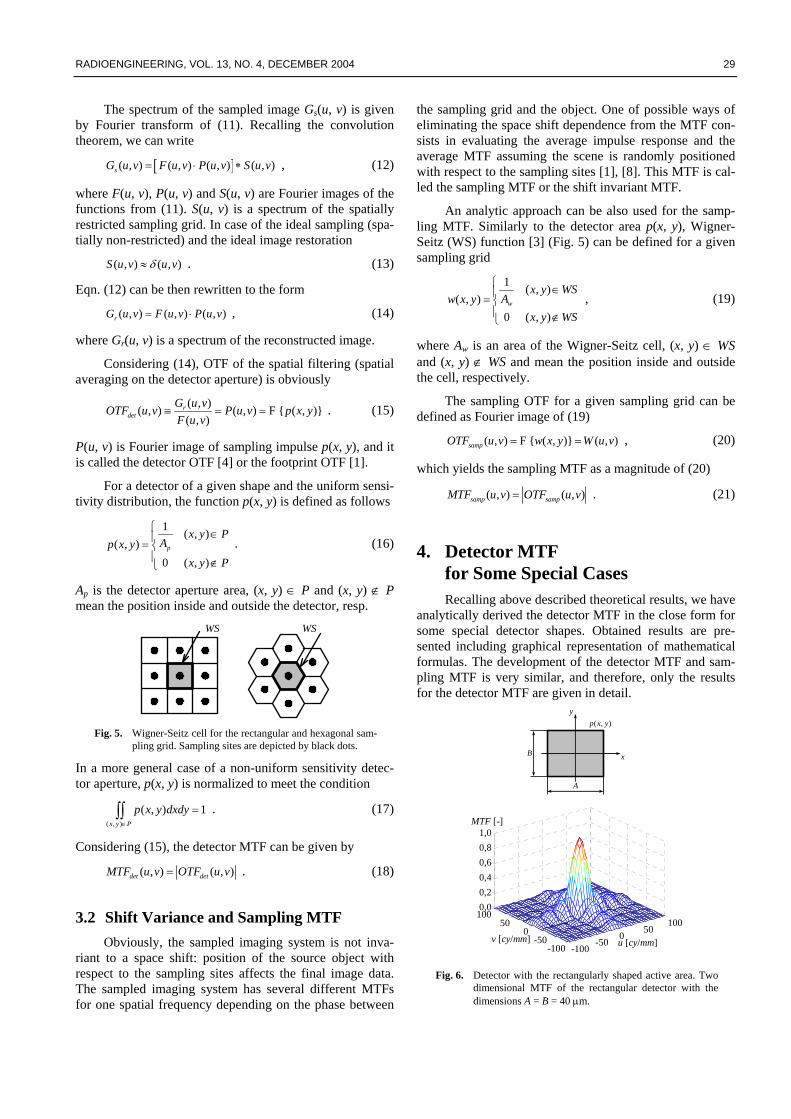
4. Detector MTF for Some Special Cases Recalling above described theoretical results, we have
analytically derived the detector MTF in the close form for some special detector shapes. Obtained results are pre-sented including graphical representation of mathematical formulas. The development of the detector MTF and sam-pling MTF is very similar, and therefore, only the results for the detector MTF are given in detail.
x
y( , )p x y
A
B
-100-50 0
50100
-100-50
050
1000,00,20,40,60,81,0
u [cy/mm]v [cy/mm]
MTF [-]
Fig. 6. Detector with the rectangularly shaped active area. Two
dimensional MTF of the rectangular detector with the dimensions A = B = 40 µm.
30 K. FLIEGEL, MODELING AND MEASUREMENT OF IMAGE SENSOR CHARACTERISTICS
4.1 Rectangularly Shaped Detector Rectangular or square detectors are rare, but play an
important role in the simplest modeling of real sensors.
According to (16), the detector function p(x, y) is
1 | | ,| |2 2( , )
0
A Bx yABp x y
elsewhere
⎧ < <⎪= ⎨⎪⎩
. (22)
The detector OTF is simply obtained Fourier transform of the separable function p(x, y)
1 1 1( , ) rect rect rect ,x yp x y x yA A B B AB A B
⎛ ⎞ ⎛ ⎞ ⎛ ⎞= ⋅ =⎜ ⎟ ⎜ ⎟ ⎜ ⎟⎝ ⎠ ⎝ ⎠ ⎝ ⎠
, (23)
( , ) { ( , )}sinc( ) sinc( ) sinc( , )
detOTF u v p x yAu Bv Au B
== ⋅ =
Fv
, (24)
where sinc(x) = sin(πx) / (πx), and
( , ) ( , ) sinc( , )det detMTF u v OTF u v Au Bv= = . (25)
Eqn. (25) shows that the transfer function is broader for smaller detector area and vice versa. This features imaging systems, which image sensors consist of rectangular detec-tors. The detector of a rectangularly shaped active area and 2D graphical representation of MTF are shown in Fig. 6.
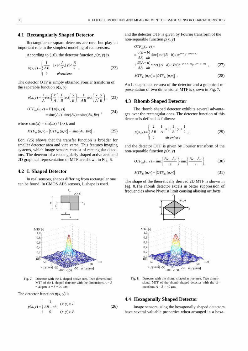
4.2 L Shaped Detector In real sensors, shapes differing from rectangular one
can be found. In CMOS APS sensors, L shape is used.
x
y( , )p x y
A
B
a
b
-100-50 0
50100
-100-50
050
1000,00,20,40,60,81,0
u [cy/mm]v [cy/mm]
MTF [-]
Fig. 7. Detector with the L shaped active area. Two dimensional
MTF of the L shaped detector with the dimensions A = B = 40 µm, a = b = 20 µm.
The detector function p(x, y) is
1 ( , )( , )
0 ( , )
x y Pp x y AB ab
x y P
⎧ ∈⎪= −⎨⎪ ∉⎩
(26)
and the detector OTF is given by Fourier transform of the non-separable function p(x, y)
( )
( )
( )
( ) ( 2 )
( , )( ) sinc ,( )
( ) sinc ( ) ,
det
j ua j v B b
j u A a j v B b
OTF u va B b au B b v e eAB abB A a A a u Bv e eAB ab
π π
π π
− −
− − − −
=−
= −−−
+ −−
, (27)
( , ) ( , )det detMTF u v OTF u v= . (28)
An L shaped active area of the detector and a graphical re-presentation of two dimensional MTF is shown in Fig. 7.
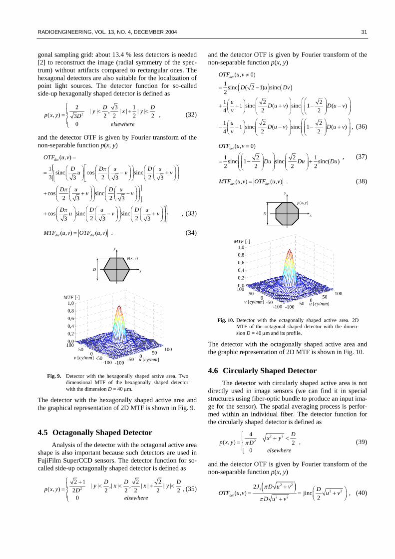
4.3 Rhomb Shaped Detector The rhomb shaped detector exhibits several advanta-
ges over the rectangular ones. The detector function of this detector is defined as follows:
2 1 1 1| | | |2( , )
0
x yAB A Bp x y
elsewhere
⎧ + <⎪= ⎨⎪⎩
, (29)
and the detector OTF is given by Fourier transform of the non-separable function p(x, y)
( , ) sinc sinc2 2det
Bv Au Bv AuOTF u v +⎛ ⎞ ⎛= ⋅⎜ ⎟ ⎜⎝ ⎠ ⎝
− ⎞⎟⎠
(30)
( , ) ( , )det detMTF u v OTF u v= (31)
The shape of the theoretically derived 2D MTF is shown in Fig. 8.The rhomb detector excels in better suppression of frequencies above Nyquist limit causing aliasing artifacts.
x
y
( , )p x y
A
B
-100-50 0
50100
-100-50
050
1000,00,20,40,60,81,0
u [cy/mm]v [cy/mm]
MTF [-]
Fig. 8. Detector with the rhomb shaped active area. Two dimen-
sional MTF of the rhomb shaped detector with the di-mensions A = B = 40 µm.
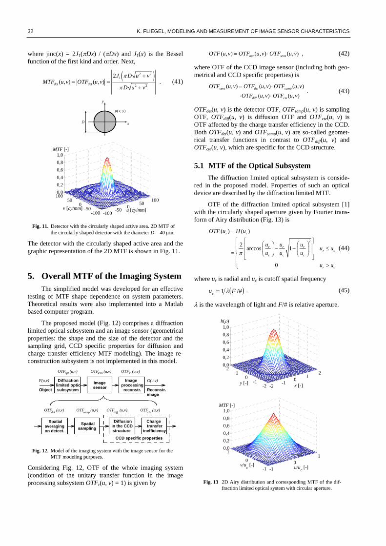
4.4 Hexagonally Shaped Detector Image sensors using the hexagonally shaped detectors
have several valuable properties when arranged in a hexa-
RADIOENGINEERING, VOL. 13, NO. 4, DECEMBER 2004 31
gonal sampling grid: about 13.4 % less detectors is needed [2] to reconstruct the image (radial symmetry of the spec-trum) without artifacts compared to rectangular ones. The hexagonal detectors are also suitable for the localization of point light sources. The detector function for so-called side-up hexagonally shaped detector is defined as
2
2 3 1| | , | | | |( , ) 2 2 2 23
0
D Dy x yp x y D
elsewhere
⎧< +⎪= ⎨
⎪⎩
< , (32)
and the detector OTF is given by Fourier transform of the non-separable function p(x, y)
( , )
1 sinc cos sinc3 2 23 3 3
cos sinc2 23 3
cos sinc sinc2 23 3 3
detOTF u v
D D u D uu v
D u D uv v
D D u D uu v v
π
π
π
=
⎧ ⎡ ⎛ ⎞ ⎛⎛ ⎞ ⎛ ⎞ ⎛ ⎞⎪= −⎨ ⎢ ⎜ ⎟ ⎜⎜ ⎟ ⎜ ⎟ ⎜ ⎟⎝ ⎠ ⎝ ⎠ ⎝ ⎠⎝ ⎠ ⎝⎪ ⎣⎩
⎤⎛ ⎞ ⎛ ⎞⎛ ⎞ ⎛ ⎞+ + − ⎥⎜ ⎟ ⎜ ⎟⎜ ⎟ ⎜ ⎟⎝ ⎠ ⎝ ⎠⎝ ⎠ ⎝ ⎠⎦
⎫⎛ ⎞ ⎛ ⎞⎛ ⎞ ⎛ ⎞ ⎛ ⎞ ⎪+ − ⎬⎜ ⎟ ⎜ ⎟⎜ ⎟ ⎜ ⎟ ⎜ ⎟⎝ ⎠ ⎝ ⎠ ⎝ ⎠ ⎪⎝ ⎠ ⎝ ⎠⎭
v⎞
+ ⎟⎠
+ , (33)
( , ) ( , )det detMTF u v OTF u v= . (34)
x
y
( , )p x y
D
-100-50 0
50100
-100-50
050
1000,00,20,40,60,81,0
u [cy/mm]v [cy/mm]
MTF [-]
Fig. 9. Detector with the hexagonally shaped active area. Two
dimensional MTF of the hexagonally shaped detector with the dimension D = 40 µm.
The detector with the hexagonally shaped active area and the graphical representation of 2D MTF is shown in Fig. 9.
4.5 Octagonally Shaped Detector Analysis of the detector with the octagonal active area
shape is also important because such detectors are used in FujiFilm SuperCCD sensors. The detector function for so-called side-up octagonally shaped detector is defined as
2
2 1 2 2| | ,| | , | | | |( , ) 2 2 2 2 20
D Dy x x yp x y Delsewhere
⎧ +< < + <⎪= ⎨
⎪⎩2D
, (35)
and the detector OTF is given by Fourier transform of the non-separable function p(x, y)
( ) ( )
( , 0)1 sinc ( 2 1) sinc2
1 2 21 sinc ( ) sinc 1 ( )4 2 2
1 2 21 sinc ( ) sinc 1 ( )4 2 2
detOTF u v
D u Dv
u D u v D u vv
u D u v D u vv
≠
= −
⎛ ⎞⎛ ⎞ ⎛ ⎞⎛ ⎞+ + + − −⎜ ⎟⎜ ⎟ ⎜ ⎟⎜ ⎟ ⎜ ⎟ ⎜ ⎟⎜ ⎟⎝ ⎠ ⎝ ⎠ ⎝ ⎠⎝ ⎠⎛ ⎞⎛ ⎞ ⎛ ⎞⎛ ⎞− − − − +⎜ ⎟⎜ ⎟ ⎜ ⎟⎜ ⎟ ⎜ ⎟ ⎜ ⎟⎜ ⎟⎝ ⎠ ⎝ ⎠ ⎝ ⎠⎝ ⎠
, (36)
( , 0)
1 2 2 1sinc 1 sinc sinc( )2 2 2 2
detOTF u v
Du Du Du
=
⎛ ⎞⎛ ⎞ ⎛ ⎞= − +⎜ ⎟⎜ ⎟ ⎜ ⎟⎜ ⎟ ⎜ ⎟⎜ ⎟⎝ ⎠ ⎝ ⎠⎝ ⎠
, (37)
( , ) ( , )det detMTF u v OTF u v= . (38)
x
y
( , )p x y
D
-100-50 0
50100
-100-50
050
1000,00,20,40,60,81,0
u [cy/mm]v [cy/mm]
MTF [-]
Fig. 10. Detector with the octagonally shaped active area. 2D
MTF of the octagonal shaped detector with the dimen-sion D = 40 µm and its profile.
The detector with the octagonally shaped active area and the graphic representation of 2D MTF is shown in Fig. 10.
4.6 Circularly Shaped Detector The detector with circularly shaped active area is not
directly used in image sensors (we can find it in special structures using fiber-optic bundle to produce an input ima-ge for the sensor). The spatial averaging process is perfor-med within an individual fiber. The detector function for the circularly shaped detector is defined as
2 22
4( , ) 2
0
Dx yp x y D
elsewhereπ
⎧ + <⎪= ⎨⎪⎩
, (39)
and the detector OTF is given by Fourier transform of the non-separable function p(x, y)
( )2 21 2 2
2 2
2( , ) jinc
2det
J D u v DOTF u v u vD u v
π
π
+ ⎛ ⎞= = ⎜ ⎟⎝ ⎠+
+ , (40)
32 K. FLIEGEL, MODELING AND MEASUREMENT OF IMAGE SENSOR CHARACTERISTICS
where jinc(x) = 2J1(πDx) / (πDx) and J1(x) is the Bessel function of the first kind and order. Next,
( )2 21
2 2
2( , ) ( , )det det
J D u vMTF u v OTF u v
D u v
π
π
+= =
+ . (41)
x
y
( , )p x y
D
-100-50 0
50100
-100-50
050
1000,00,20,40,60,81,0
u [cy/mm]v [cy/mm]
MTF [-]
Fig. 11. Detector with the circularly shaped active area. 2D MTF of
the circularly shaped detector with the diameter D = 40 µm.
The detector with the circularly shaped active area and the graphic representation of the 2D MTF is shown in Fig. 11.
5. Overall MTF of the Imaging System The simplified model was developed for an effective
testing of MTF shape dependence on system parameters. Theoretical results were also implemented into a Matlab based computer program.
The proposed model (Fig. 12) comprises a diffraction limited optical subsystem and an image sensor (geometrical properties: the shape and the size of the detector and the sampling grid, CCD specific properties for diffusion and charge transfer efficiency MTF modeling). The image re-construction subsystem is not implemented in this model.
Diffraction limited opticsubsystem Reconstr.
image
F(u,v)
ObjectImage Image
reconstr.
G(u,v)
optOTF (u,v) sensOTF (u,v) rOTF (u,v)
detOTF (u,v) sampOTF (u,v) diffOTF (u,v) cteOTF (u,v)
CCD specific properties
sensor processing
Spatial averagingon detect.
Spatial Diffusion
structuresampling in the CCD Chargetransfer
inefficiency
Fig. 12. Model of the imaging system with the image sensor for the
MTF modeling purposes.
Considering Fig. 12, OTF of the whole imaging system (condition of the unitary transfer function in the image processing subsystem OTFr(u, v) = 1) is given by
( , ) ( , ) ( , )opt sensOTF u v OTF u v OTF u v= ⋅ , (42)
where OTF of the CCD image sensor (including both geo-metrical and CCD specific properties) is
( , ) ( , ) ( , )
( , ) ( , )sens det samp
diff cte
OTF u v OTF u v OTF u v
OTF u v OTF u v
= ⋅
⋅ ⋅ . (43)
OTFdet(u, v) is the detector OTF, OTFsamp(u, v) is sampling OTF, OTFdiff(u, v) is diffusion OTF and OTFcte(u, v) is OTF affected by the charge transfer efficiency in the CCD. Both OTFdet(u, v) and OTFsamp(u, v) are so-called geomet-rical transfer functions in contrast to OTFdiff(u, v) and OTFcte(u, v), which are specific for the CCD structure.
5.1 MTF of the Optical Subsystem The diffraction limited optical subsystem is conside-
red in the proposed model. Properties of such an optical device are described by the diffraction limited MTF.
OTF of the diffraction limited optical subsystem [1] with the circularly shaped aperture given by Fourier trans-form of Airy distribution (Fig. 13) is
2
( ) ( )
2 arccos 1
0
r r
r r rr
c c c
r c
OTF u H u
u u u u uu u u
u u
π
=
⎧ ⎡ ⎤⎛ ⎞ ⎛ ⎞⎪ ⎢ ⎥− − ≤⎜ ⎟ ⎜ ⎟⎪ ⎢ ⎥= ⎨ ⎝ ⎠ ⎝ ⎠⎣ ⎦⎪⎪ >⎩
c (44)
where ur is radial and uc is cutoff spatial frequency
( )/#1 Fuc λ= . (45)
λ is the wavelength of light and F/# is relative aperture.
-2-1 0
12
-2-1
01
20,00,20,40,60,81,0
x [-]y [-]
h(ρ)
-10
1
-1
0
10,00,20,40,60,81,0
u/uc [-]v/uc [-]
MTF [-]
Fig. 13 2D Airy distribution and corresponding MTF of the dif-
fraction limited optical system with circular aperture.
RADIOENGINEERING, VOL. 13, NO. 4, DECEMBER 2004 33
[ / ]u cy mm
[ ]diffMTF −
0 10 20 30 40 500,0
0,2
0,4
0,6
0,8
1,0 0, 4 mλ µ=
0, 7 mλ µ=
0,85 mλ µ=
0,0
0,2
0,4
0,6
0,8
1,0 [ ]cteMTF −
[ ]u x⋅ ∆ −1/ 4 1/ 20
0,9999CTE =
0,999CTE =
512N =
1024N =
512N =
1024N =
Fig. 14. Diffusion MTF and charge transfer efficiency MTF in the
CCD specific subsystem model.
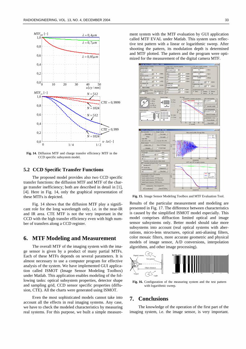
5.2 CCD Specific Transfer Functions The proposed model provides also two CCD specific
transfer functions: the diffusion MTF and MTF of the char-ge transfer inefficiency; both are described in detail in [1], [4]. Here in Fig. 14, only the graphical representation of these MTFs is depicted.
Fig. 14 shows that the diffusion MTF play a signifi-cant role for the long wavelength only, i.e. in the near-IR and IR area. CTE MTF is not the very important in the CCD with the high transfer efficiency even with high num-ber of transfers along a CCD register.
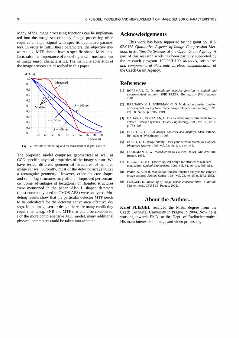
6. MTF Modeling and Measurement The overall MTF of the imaging system with the ima-
ge sensor is given by a product of many partial MTFs. Each of these MTFs depends on several parameters. It is almost necessary to use a computer program for effective analysis of the system. We have implemented GUI applica-tion called ISMOT (Image Sensor Modeling Toolbox) under Matlab. This application enables modeling of the fol-lowing tasks: optical subsystem properties, detector shape and sampling grid, CCD sensor specific properties (diffu-sion, CTE). All the charts were generated using ISMOT.
Even the most sophisticated models cannot take into account all the effects in real imaging systems. Any case, we have to check the modeled characteristics by measuring real systems. For this purpose, we built a simple measure-
ment system with the MTF evaluation by GUI application called MTF EVAL under Matlab. This system uses reflec-tive test pattern with a linear or logarithmic sweep. After shooting the pattern, its modulation depth is determined and MTF plotted. The pattern and the program were opti-mized for the measurement of the digital camera MTF.
Fig. 15. Image Sensor Modeling Toolbox and MTF Evaluation Tool.
Results of the particular measurement and modeling are presented in Fig. 17. The difference between characteristics is caused by the simplified ISMOT model especially. This model comprises diffraction limited optical and image sensor subsystems only. Better model should take more subsystems into account (real optical systems with aber-rations, micro-lens structures, optical anti-aliasing filters, color mosaic filters, more accurate geometric and physical models of image sensor, A/D conversions, interpolation algorithms, and other image processing).
Digital camera
Test pattern
Tripod Light
Object distance
Fig. 16. Configuration of the measuring system and the test pattern
with logarithmic sweep.
7. Conclusions The knowledge of the operation of the first part of the
imaging system, i.e. the image sensor, is very important.
34 K. FLIEGEL, MODELING AND MEASUREMENT OF IMAGE SENSOR CHARACTERISTICS
Many of the image processing functions can be implemen-ted into the image sensor today. Image processing often requires an input signal with specific qualitative parame-ters. In order to fulfill these parameters, the objective me-asures e.g. MTF should have a specific shape. Mentioned facts raise the importance of modeling and/or measurement of image sensor characteristics. The main characteristics of the image sensors are described in this paper.
0 20 40 60 80 100 120 140 160 180 2000,0
0,1
0,2
0,3
0,4
0,5
0,6
0,7
0,8
0,9
1,0 MTF [-]
u [cy/mm]
Measured
Modeled
400nmλ =
555nmλ =
800nmλ =
Fig. 17. Results of modeling and measurement of digital camera.
The proposed model comprises geometrical as well as CCD specific physical properties of the image sensor. We have tested different geometrical structures of an area image sensor. Currently, most of the detector arrays utilize a rectangular geometry. However, other detector shapes and sampling structures may offer an improved performan-ce. Some advantages of hexagonal or rhombic structures were mentioned in the paper. Also L shaped detectors (most commonly used in CMOS APS) were analyzed. Mo-deling results show that the particular detector MTF needs to be calculated for the detector active area effective de-sign. In the image sensor design there are many conflicting requirements e.g. SNR and MTF that could be considered. For the more comprehensive MTF model, many additional physical parameters could be taken into account.
Acknowledgements This work has been supported by the grant no. 102/
02/0133 Qualitative Aspects of Image Compression Met-hods in Multimedia Systems of the Czech Grant Agency. A part of this research work has been partially supported by the research program 102/03/H109 Methods, structures and components of electronic wireless communication of the Czech Grant Agency.
References [1] BOREMAN, G. D. Modulation transfer function in optical and
electro-optical systems. SPIE PRESS, Bellingham (Washington), 2001.
[2] BARNARD, K. J., BOREMAN, G. D. Modulation transfer function of hexagonal staring focal plane arrays. Optical Engineering, 1991, vol. 30, no. 12, p. 1915–1919.
[3] HADAR, O., BOREMAN, G. D. Oversampling requirements for pi-xelated – imager systems. Optical Engineering, 1999, vol. 38, no. 5, p. 782–785.
[4] HOLST, G. C. CCD arrays, cameras and displays, SPIE PRESS, Bellingham (Washington), 1998.
[5] HOLST, G. C. Image quality: Does your detector match your optics? Photonics Spectra, 1999, vol. 33, no. 1, p. 144–146.
[6] GOODMAN, J. W. Introduction to Fourier Optics. McGraw-Hill, Boston, 1996.
[7] HUCK, F. O. et al. Electro-optical design for efficient visual com-munication. Optical Engineering, 1996, vol. 34, no. 1, p. 795–813.
[8] PARK, S. K. et al. Modulation-transfer-function analysis for sampled image systems. Applied Optics, 1984, vol. 23, no. 15, p. 2572–2582.
[9] FLIEGEL, K. Modeling of image sensor characteristics in Matlab. Master thesis, CTU FEE, Prague, 2004.
About the Author... Karel FLIEGEL received the M.Sc. degree from the Czech Technical University in Prague in 2004. Now he is working towards Ph.D. at the Dept. of Radioelectronics. His main interest is in image and video processing.