Embed Size (px)
Citation preview
Modeling and mitigating pattern andModeling and mitigating pattern and process dependencies in nanoimprintlithographylithography23 June 201123 June 2011Hayden Taylor Singapore-MIT Alliance for Research and Technology
formerly based at: Microsystems Technology Laboratories MITMicrosystems Technology Laboratories, MIT
Collaborators and acknowledgements
• Funding • MIT• Singapore-MIT Alliance• Danish National Advanced
Technology Foundation
• Duane Boning• Cai Gogwilt• Matt DirckxTechnology Foundation
• NIL TechnologyKristian Smistrup
• Matt Dirckx• Eehern Wong• Melinda Hale
• Kristian Smistrup• Theodor Nielsen • Brian Bilenberg
• Helpful discussions• Hella Scheerg
• University of California, San Diego• Andrew Kahng
Hella Scheer• Yoshihiko Hirai• Dave White
• Andrew Kahng• Yen-Kuan Wu
2
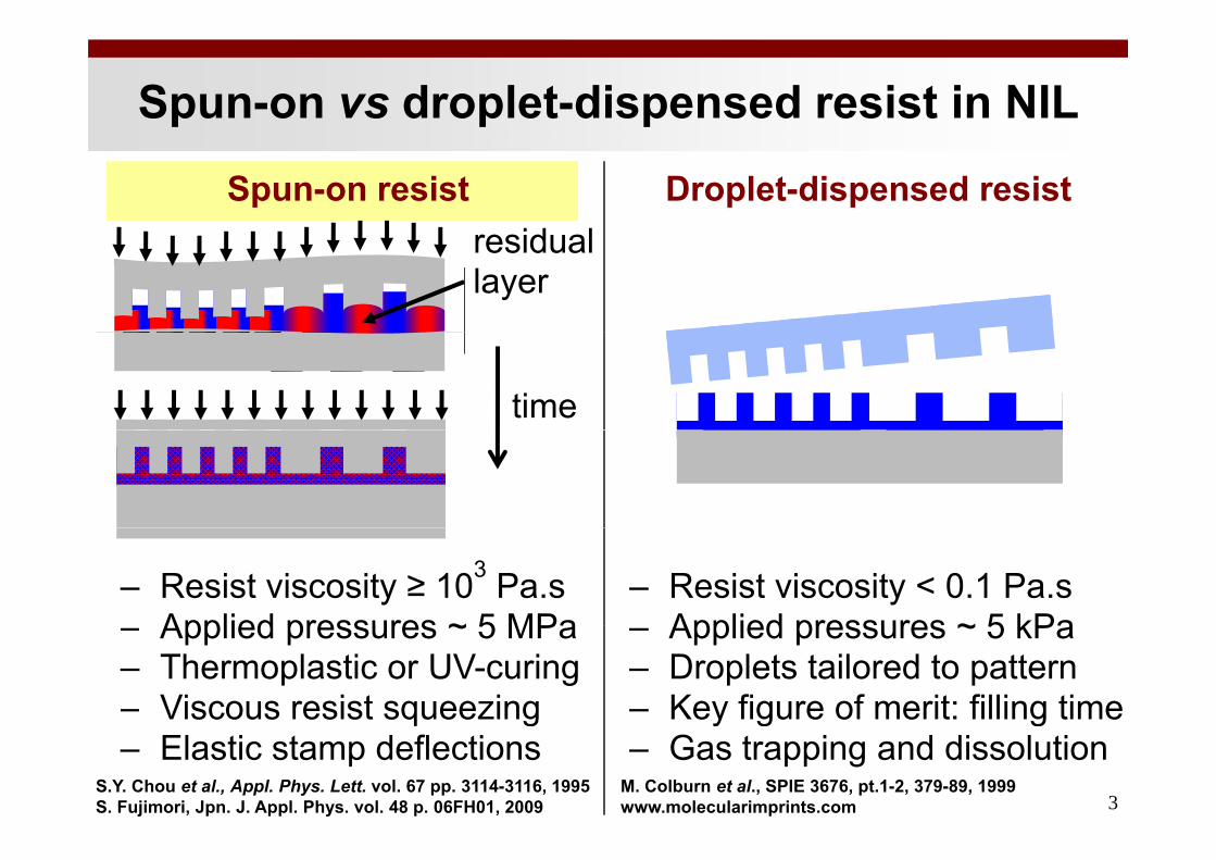
Spun-on vs droplet-dispensed resist in NIL
Spun-on resist Droplet-dispensed resistresidualresiduallayer
time
– Resist viscosity ≥ 103 Pa.sApplied pressures ~ 5 MPa
– Resist viscosity < 0.1 Pa.sApplied pressures ~ 5 kPa– Applied pressures ~ 5 MPa
– Thermoplastic or UV-curing– Viscous resist squeezing
– Applied pressures ~ 5 kPa– Droplets tailored to pattern– Key figure of merit: filling time
3
q g– Elastic stamp deflections
y g g– Gas trapping and dissolution
S.Y. Chou et al., Appl. Phys. Lett. vol. 67 pp. 3114-3116, 1995S. Fujimori, Jpn. J. Appl. Phys. vol. 48 p. 06FH01, 2009
M. Colburn et al., SPIE 3676, pt.1-2, 379-89, 1999www.molecularimprints.com
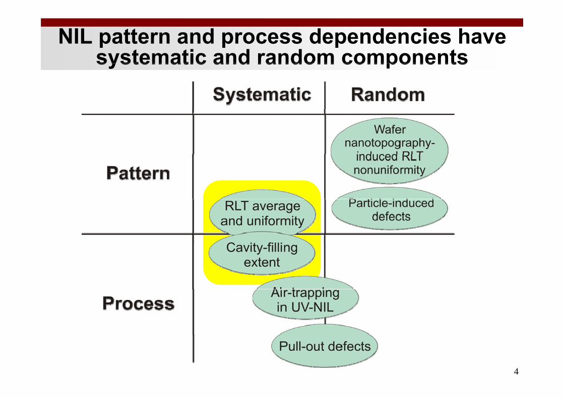
NIL pattern and process dependencies have systematic and random componentssystematic and random components
4
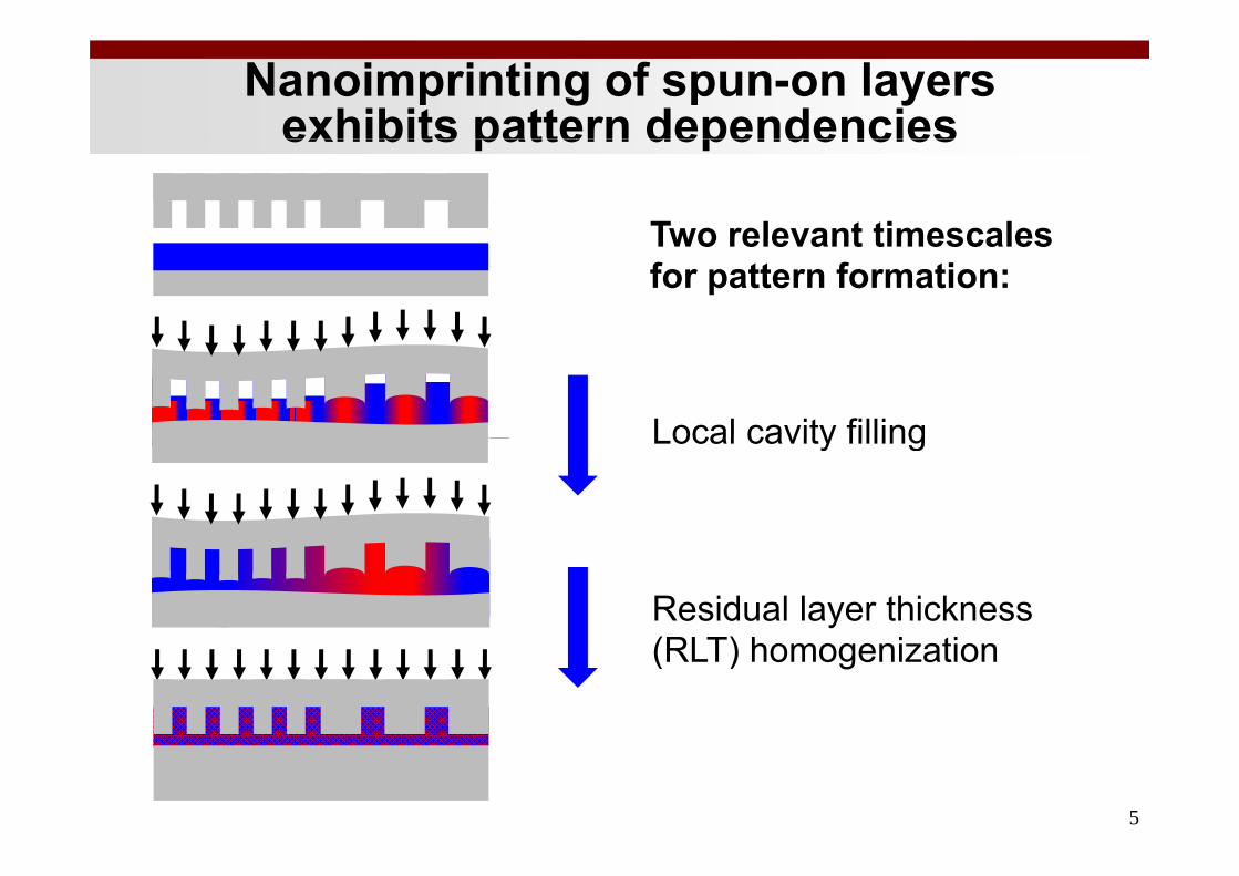
Nanoimprinting of spun-on layersexhibits pattern dependenciesexhibits pattern dependencies
Two relevant timescalesTwo relevant timescales for pattern formation:
Local cavity fillingLocal cavity filling
Residual layer thickness(RLT) h i i(RLT) homogenization
5
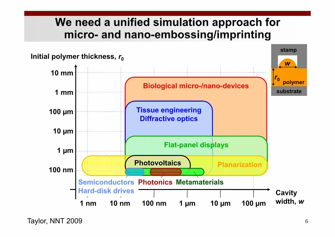
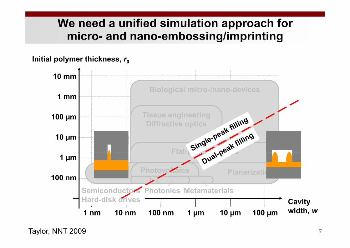
We need a unified simulation approach for micro- and nano-embossing/imprintingmicro and nano embossing/imprinting
stamp
wInitial polymer thickness, r0
polymerpolymersubstrate
w
r010 mm
1 mmBiological micro-/nano-devices
substrate1 mm
100 µm Tissue engineeringDiffractive optics
10 µmDiffractive optics
Flat-panel displays1 µm
100 nm
Flat-panel displays
PlanarizationPhotovoltaics00
Cavity idth
MetamaterialsPhotonicsSemiconductorsHard-disk drives
6
width, w1 nm 10 nm 100 nm 1 µm 10 µm 100 µm
Taylor, NNT 2009
We need a unified simulation approach for micro- and nano-embossing/imprintingmicro and nano embossing/imprinting
Initial polymer thickness, r0
Biological micro-/nano-devices
10 mm
1 mm
Tissue engineeringDiffractive optics
1 mm
100 µmDiffractive optics
Flat-panel displays
10 µm
Flat-panel displays
PlanarizationPhotovoltaics1 µm
100 nm
Cavity idth
MetamaterialsPhotonics00
SemiconductorsHard-disk drives
7
1 nm width, w1 nm 10 nm 100 nm 1 µm 10 µm 100 µm
Taylor, NNT 2009
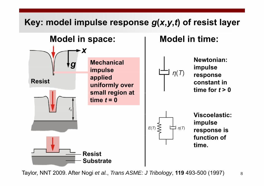
Key: model impulse response g(x,y,t) of resist layer
Model in time:Model in space:x
Newtonian: impulse
xg Mechanical
impulseresponse constant in time for t > 0
impulse applied uniformly over small region at
Resist
Viscoelastic:
small region at time t = 0
Viscoelastic: impulse response is f i f
Resist
function of time.
8
Substrate
Taylor, NNT 2009. After Nogi et al., Trans ASME: J Tribology, 119 493-500 (1997)
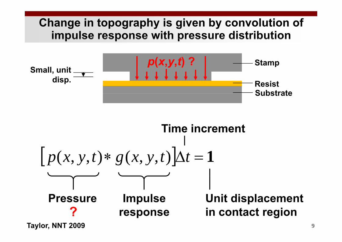
Change in topography is given by convolution of impulse response with pressure distributionimpulse response with pressure distribution
Stampp(x,y,t) ?
ResistSubstrate
pp( ,y, )Small, unit
disp.Substrate
Time increment
1 ttyxgtyxp ),,(),,(
Pressure Impulse Unit displacement
9
presponse
pin contact region?
Taylor, NNT 2009
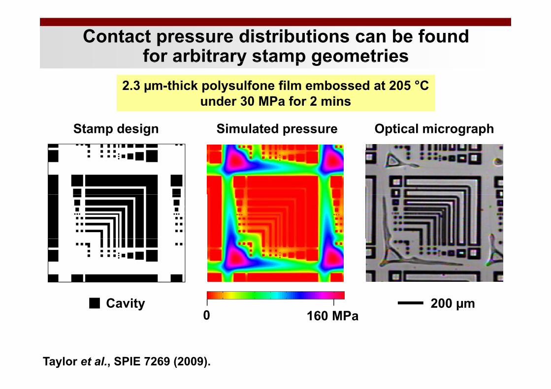
Contact pressure distributions can be found for arbitrary stamp geometrieso a b t a y sta p geo et es
2.3 µm-thick polysulfone film embossed at 205 °C under 30 MPa for 2 mins
Stamp design Simulated pressure Optical micrograph
160 MPa0Cavity 200 µm
Taylor et al., SPIE 7269 (2009).
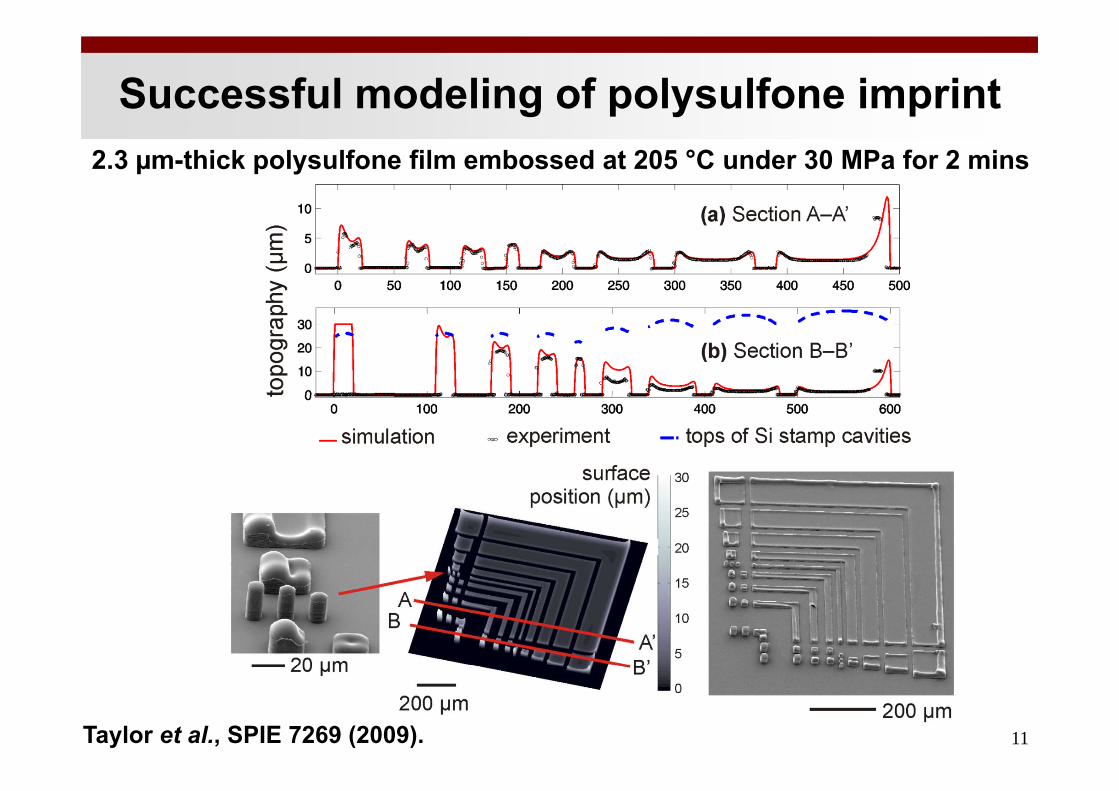
Successful modeling of polysulfone imprint2.3 µm-thick polysulfone film embossed at 205 °C under 30 MPa for 2 mins
11Taylor et al., SPIE 7269 (2009).
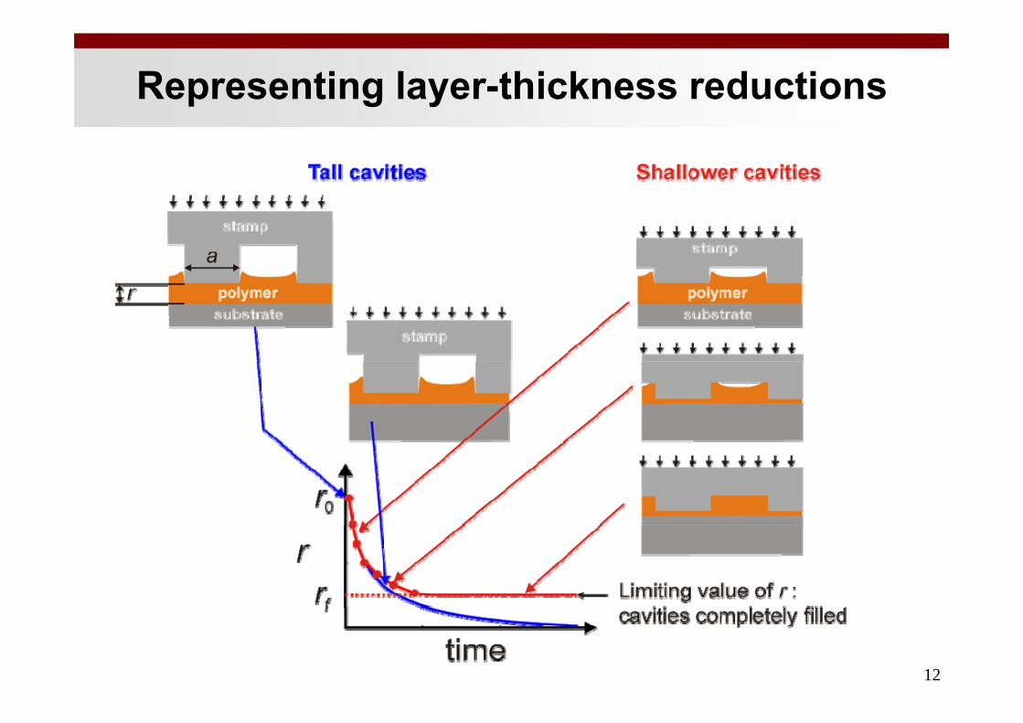
Representing layer-thickness reductions
12
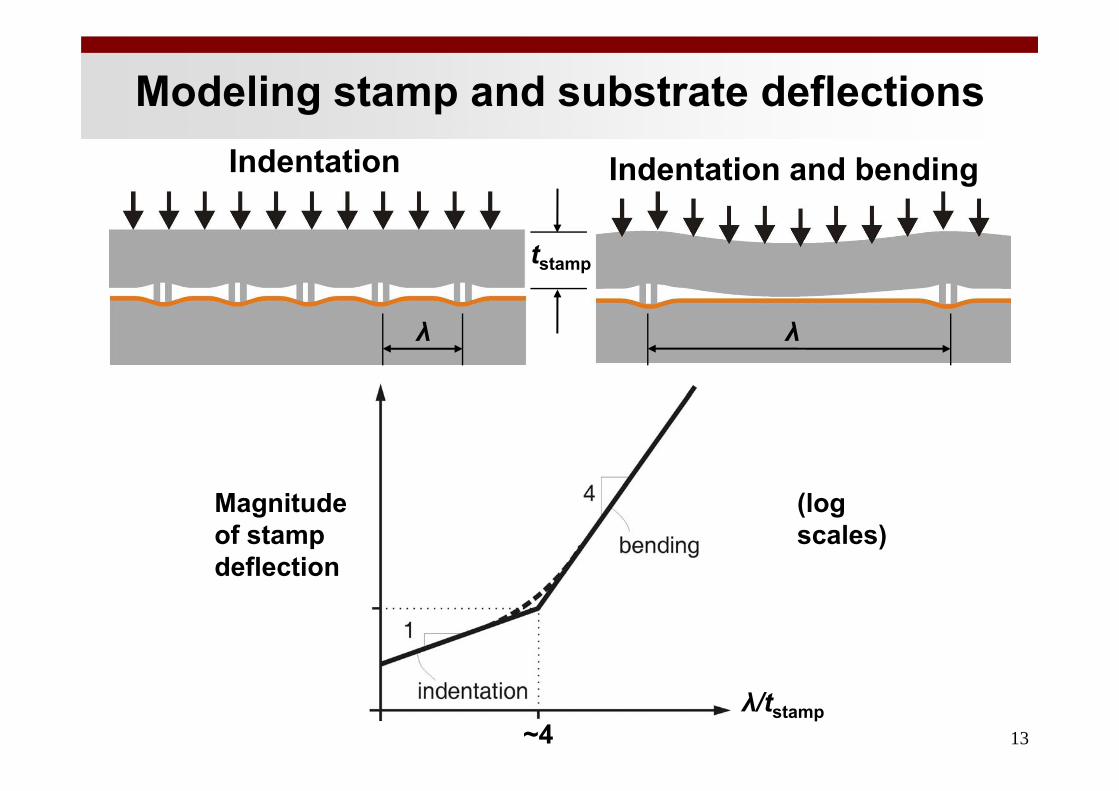
Modeling stamp and substrate deflectionsIndentation Indentation and bending
tstamp
λ λ
Magnitude of stamp deflection
(log scales)
deflection
13
λ/tstamp~4
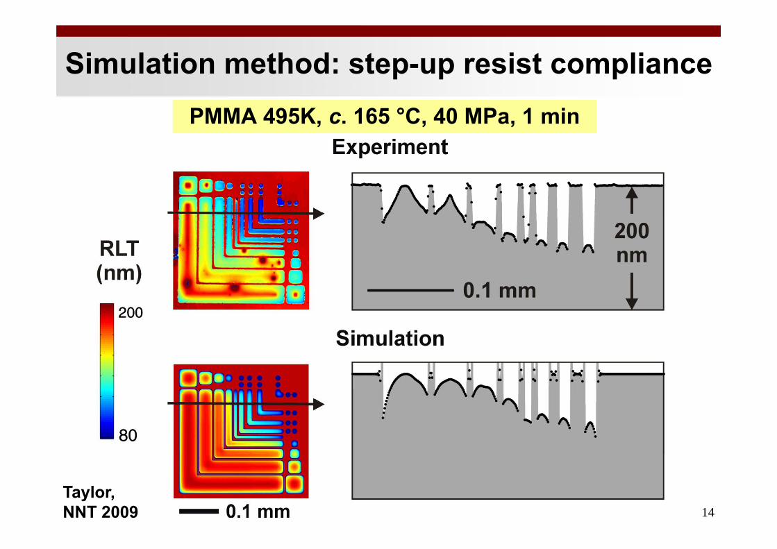
Simulation method: step-up resist compliancePMMA 495K, c. 165 °C, 40 MPa, 1 min
14Taylor, NNT 2009
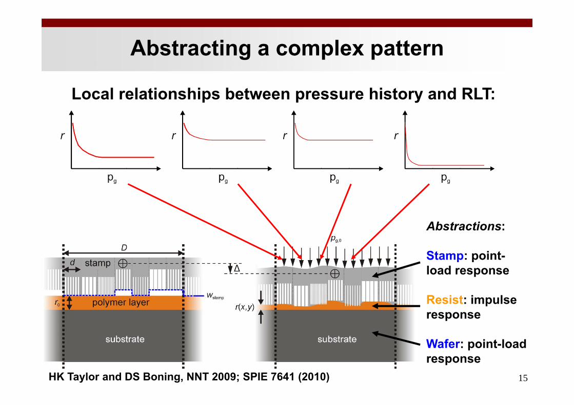
Abstracting a complex pattern
Local relationships between pressure history and RLT:
Abstractions:
Stamp: point-load response
Resist: impulse response
W f i t l d
15
Wafer: point-load response
HK Taylor and DS Boning, NNT 2009; SPIE 7641 (2010)
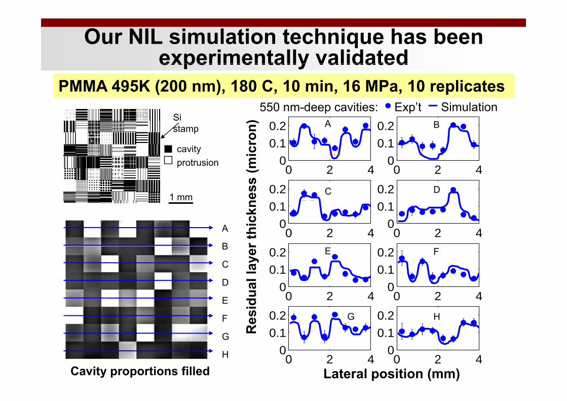
Our NIL simulation technique has been experimentally validated
PMMA 495K (200 nm), 180 C, 10 min, 16 MPa, 10 replicates550 nm-deep cavities: Exp’t Simulation
experimentally validated
Si stamp
cavity0
0.1
0.2
0
0.1
0.2
0
0.1
0.2
0
0.1
0.2
icro
n) A B
550 nm deep cavities: Exp t Simulation
1 mm
protrusion0 2 4
00 2 4
0
0.1
0.2
0.1
0.2
0 2 40
0 2 40
0.1
0.2
0.1
0.2
ness
(mi
C D
0 2 40
0.1
0 2 40
0.1
0.2 0.2
0 2 40
0.1
0 2 40
0.1
0.2 0.2r t
hick
n
A
B
0 2 40
0.1
0.2
0 2 40
0.1
0.2
0 2 40
0.1
0.2
0 2 40
0.1
0.2ua
l lay
erB
C
D
E F
0 2 40
0 2 40
0.1
0.2
0.1
0.2
0 2 40
0 2 40
0.1
0.2
0.1
0.2
Res
iduE
F
G
G H
0 2 40
0.1
0 2 40
0.1
0 2 40
0.1
0 2 40
0.1
Lateral position (mm)Cavity proportions filled
G
H
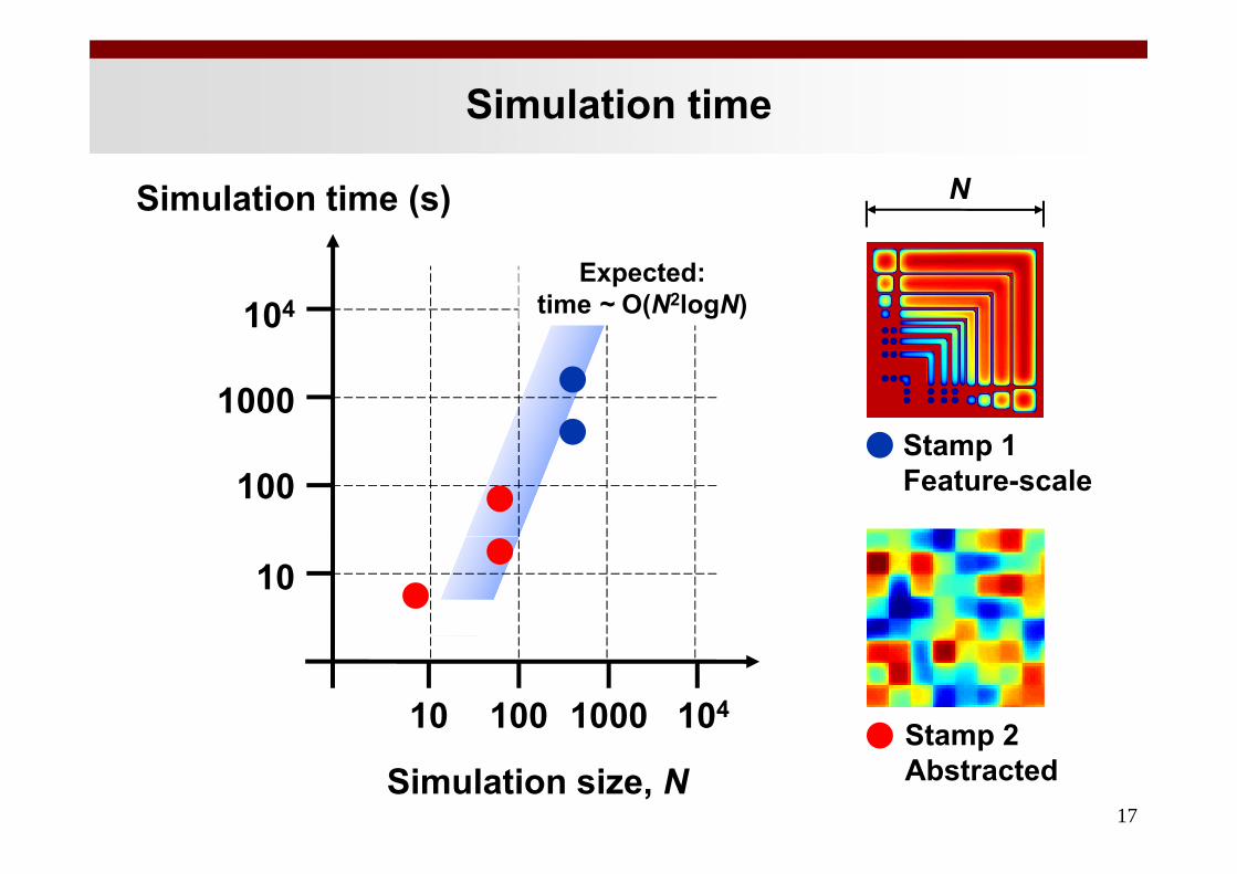
Simulation time
Simulation time (s) N
104Expected:
time ~ O(N2logN)
1000St 1
100Stamp 1Feature-scale
10
10 100 1000 104Stamp 2
17
Stamp 2AbstractedSimulation size, N
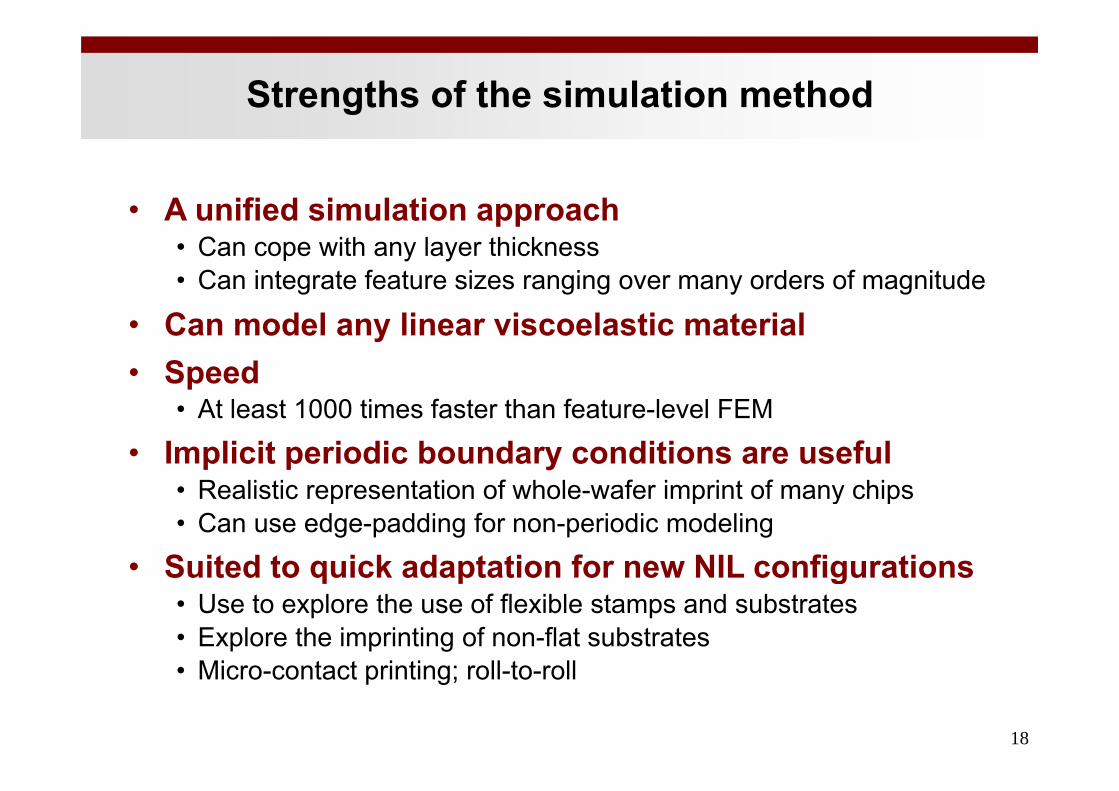
Strengths of the simulation method
• A unified simulation approachA unified simulation approach• Can cope with any layer thickness• Can integrate feature sizes ranging over many orders of magnitude
• Can model any linear viscoelastic material• Speed
• At least 1000 times faster than feature-level FEM
• Implicit periodic boundary conditions are usefulRealistic representation of whole wafer imprint of many chips• Realistic representation of whole-wafer imprint of many chips
• Can use edge-padding for non-periodic modeling
• Suited to quick adaptation for new NIL configurationsSuited to quick adaptation for new NIL configurations• Use to explore the use of flexible stamps and substrates• Explore the imprinting of non-flat substrates
Mi t t i ti ll t ll
18
• Micro-contact printing; roll-to-roll
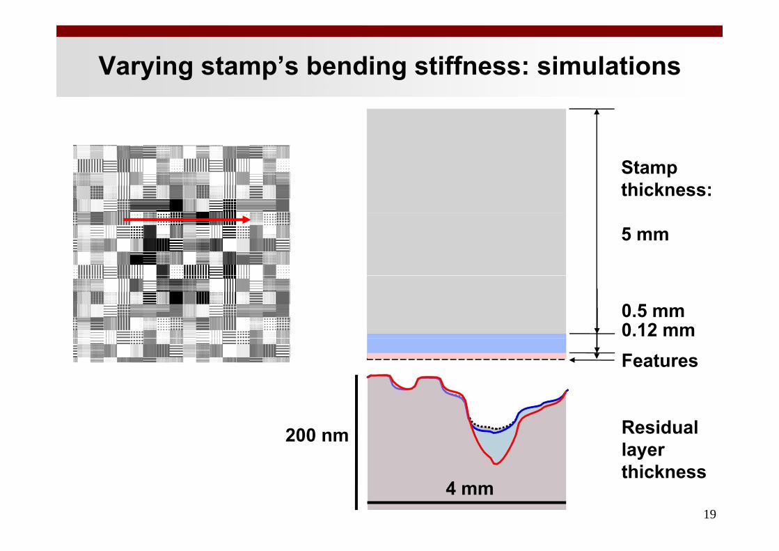
Varying stamp’s bending stiffness: simulations
Stampthickness:
5 mm
0.5 mm0.12 mmFeatures
200 nm Residual layer
19
4 mmthickness
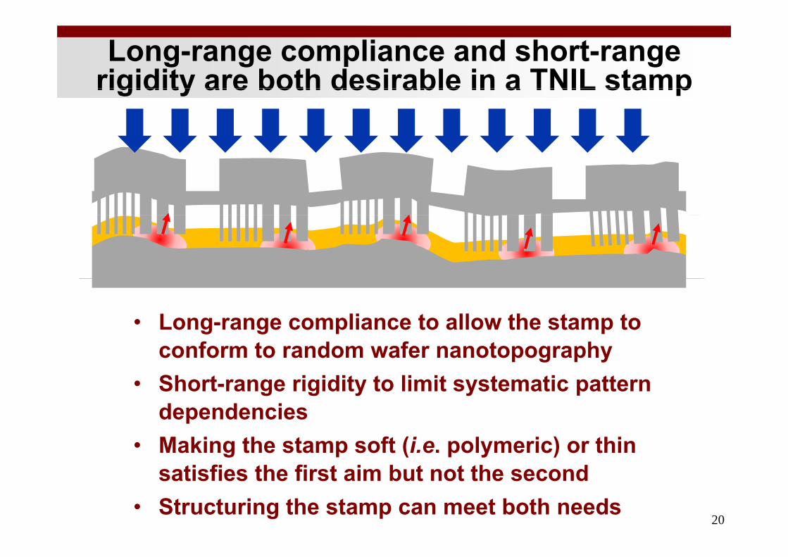
Long-range compliance and short-range rigidity are both desirable in a TNIL stamprigidity are both desirable in a TNIL stamp
• Long-range compliance to allow the stamp to f d f hconform to random wafer nanotopography
• Short-range rigidity to limit systematic pattern d d idependencies
• Making the stamp soft (i.e. polymeric) or thin ti fi th fi t i b t t th d
20
satisfies the first aim but not the second• Structuring the stamp can meet both needs
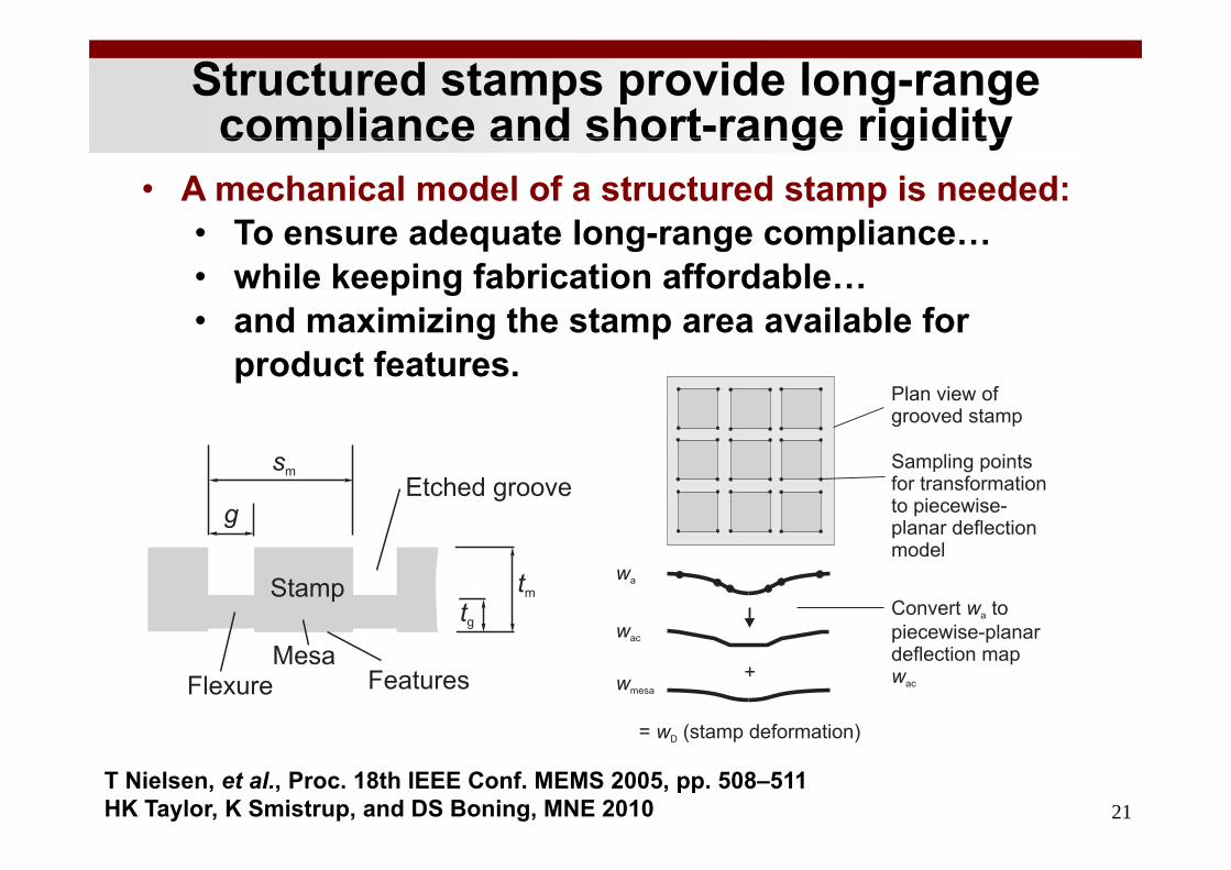
Structured stamps provide long-range compliance and short-range rigiditycompliance and short range rigidity
• A mechanical model of a structured stamp is needed:• To ensure adequate long-range complianceTo ensure adequate long-range compliance…• while keeping fabrication affordable…• and maximizing the stamp area available for g p
product features.
21T Nielsen, et al., Proc. 18th IEEE Conf. MEMS 2005, pp. 508–511 HK Taylor, K Smistrup, and DS Boning, MNE 2010
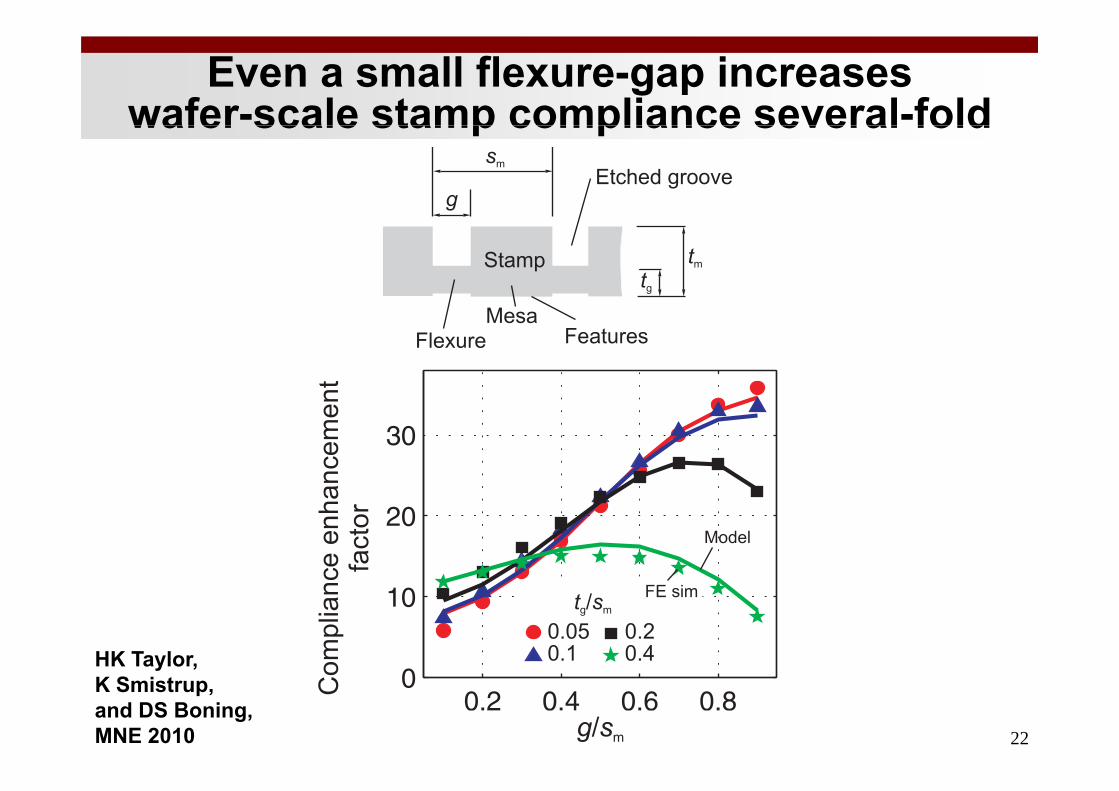
Even a small flexure-gap increases wafer-scale stamp compliance several-foldwafer scale stamp compliance several fold
HK Taylor,
22
HK Taylor, K Smistrup, and DS Boning, MNE 2010
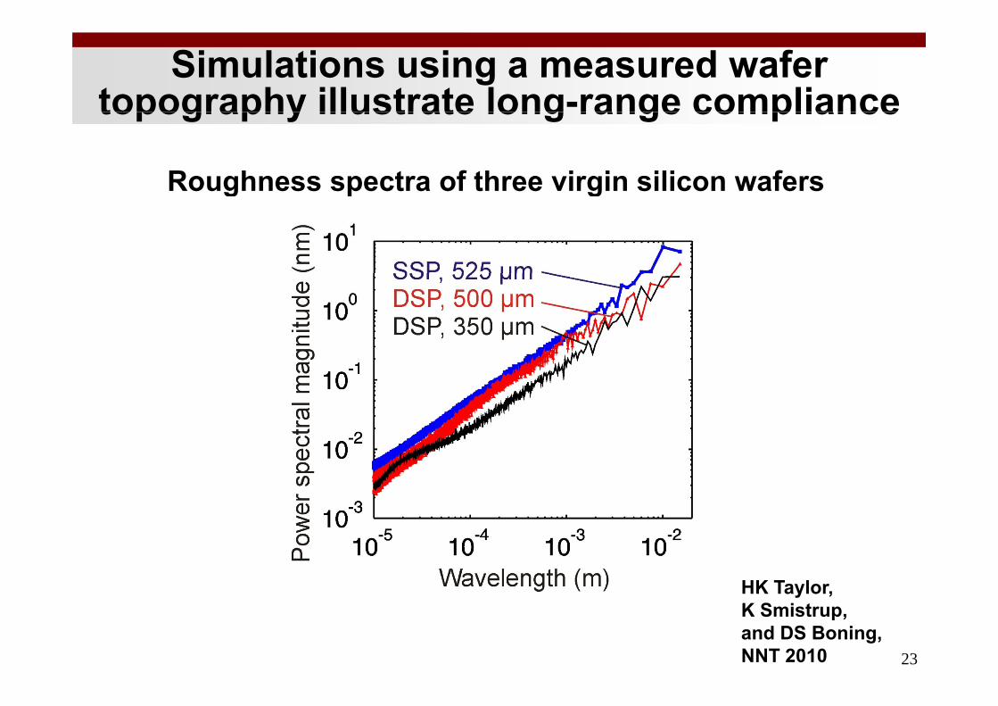
Simulations using a measured wafer topography illustrate long-range compliancetopography illustrate long range compliance
Roughness spectra of three virgin silicon wafersg p g
HK Taylor,
23
HK Taylor, K Smistrup, and DS Boning, NNT 2010
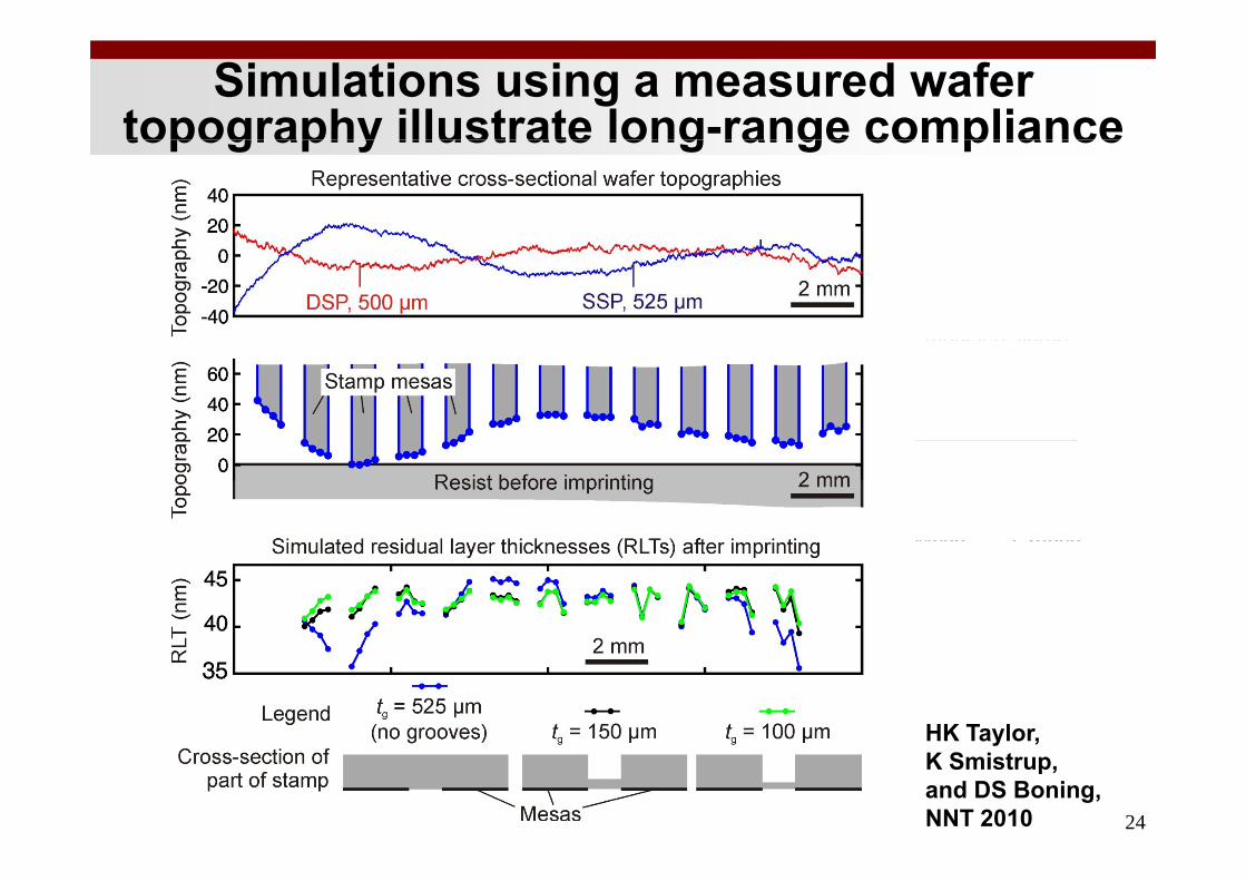
Simulations using a measured wafer topography illustrate long-range compliancetopography illustrate long range compliance
HK Taylor,
24
HK Taylor, K Smistrup, and DS Boning, NNT 2010
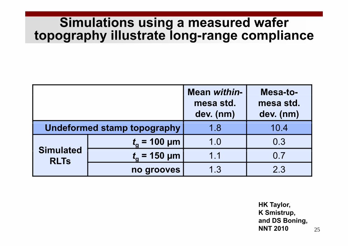
Simulations using a measured wafer topography illustrate long-range compliancetopography illustrate long range compliance
Mean within- Mesa-to-Mean withinmesa std. dev. (nm)
Mesa tomesa std. dev. (nm)
Undeformed stamp topography 1.8 10.4
Simulatedtg = 100 µm 1.0 0.3
SimulatedRLTs tg = 150 µm 1.1 0.7
no grooves 1.3 2.3
HK Taylor,
25
HK Taylor, K Smistrup, and DS Boning, NNT 2010
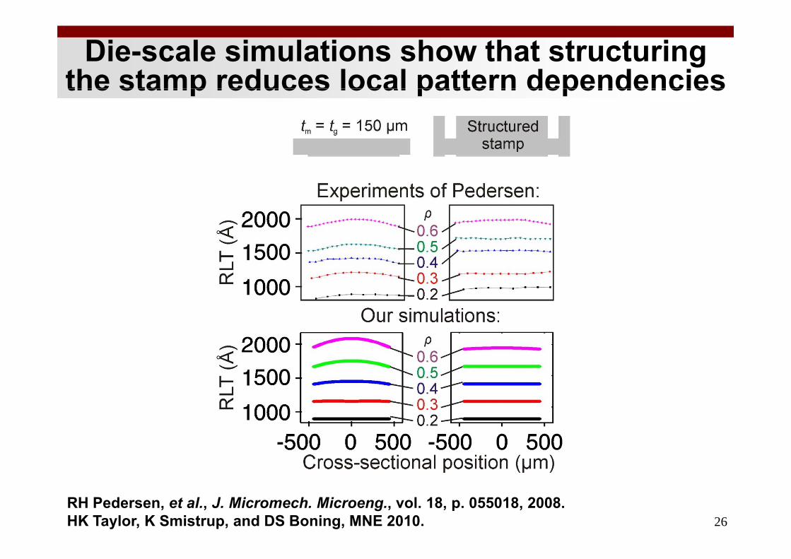
Die-scale simulations show that structuring the stamp reduces local pattern dependenciesthe stamp reduces local pattern dependencies
26RH Pedersen, et al., J. Micromech. Microeng., vol. 18, p. 055018, 2008. HK Taylor, K Smistrup, and DS Boning, MNE 2010.
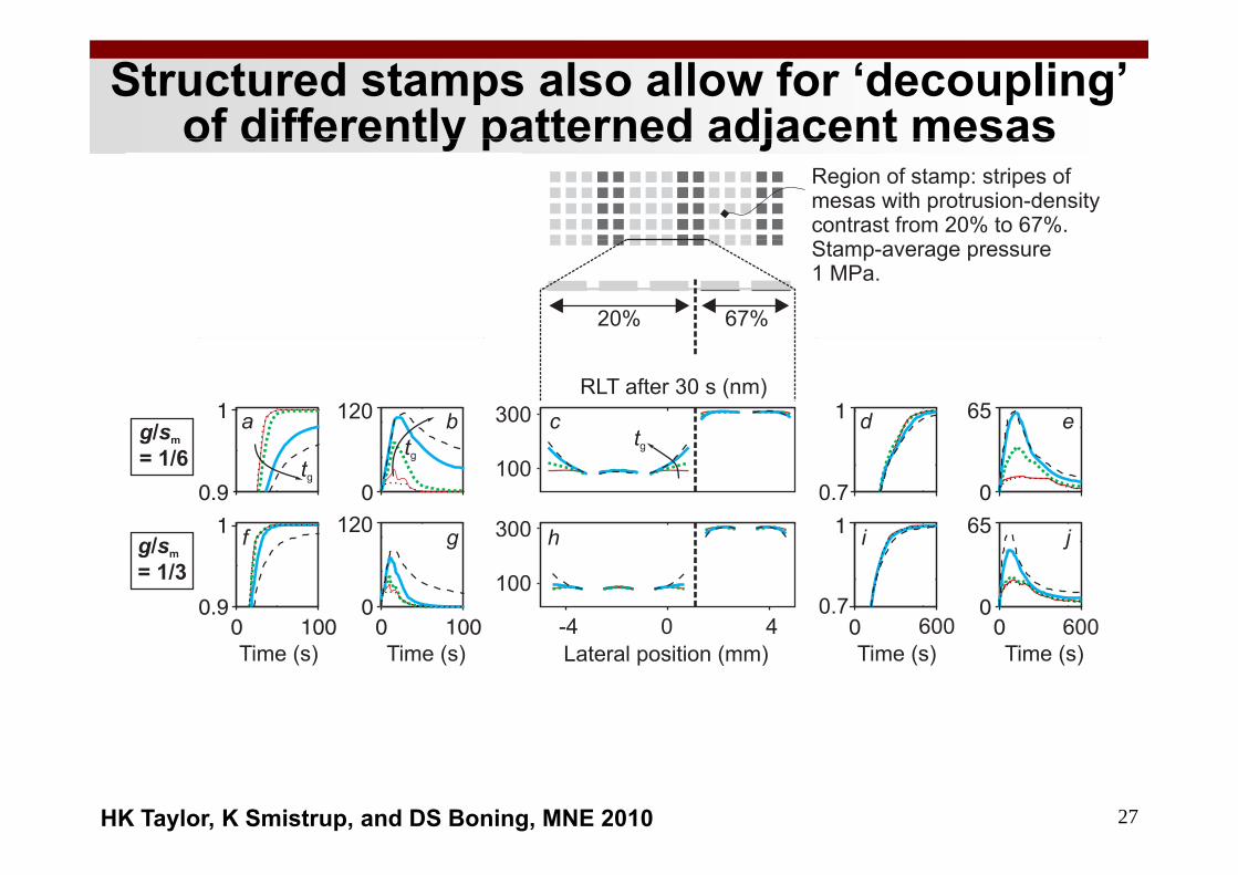
Structured stamps also allow for ‘decoupling’ of differently patterned adjacent mesasof differently patterned adjacent mesas
27HK Taylor, K Smistrup, and DS Boning, MNE 2010
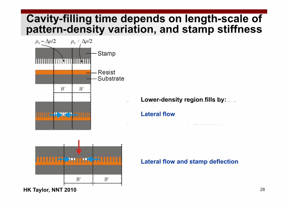
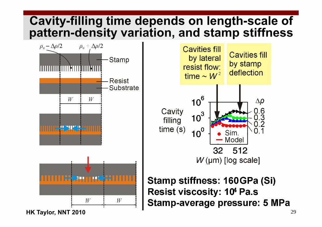
Cavity-filling time depends on length-scale of pattern-density variation, and stamp stiffnesspattern density variation, and stamp stiffness
Lower-density region fills by:
Lateral flow
Lower density region fills by:
Lateral flow and stamp deflection
28HK Taylor, NNT 2010
Cavity-filling time depends on length-scale of pattern-density variation, and stamp stiffnesspattern density variation, and stamp stiffness
29HK Taylor, NNT 2010
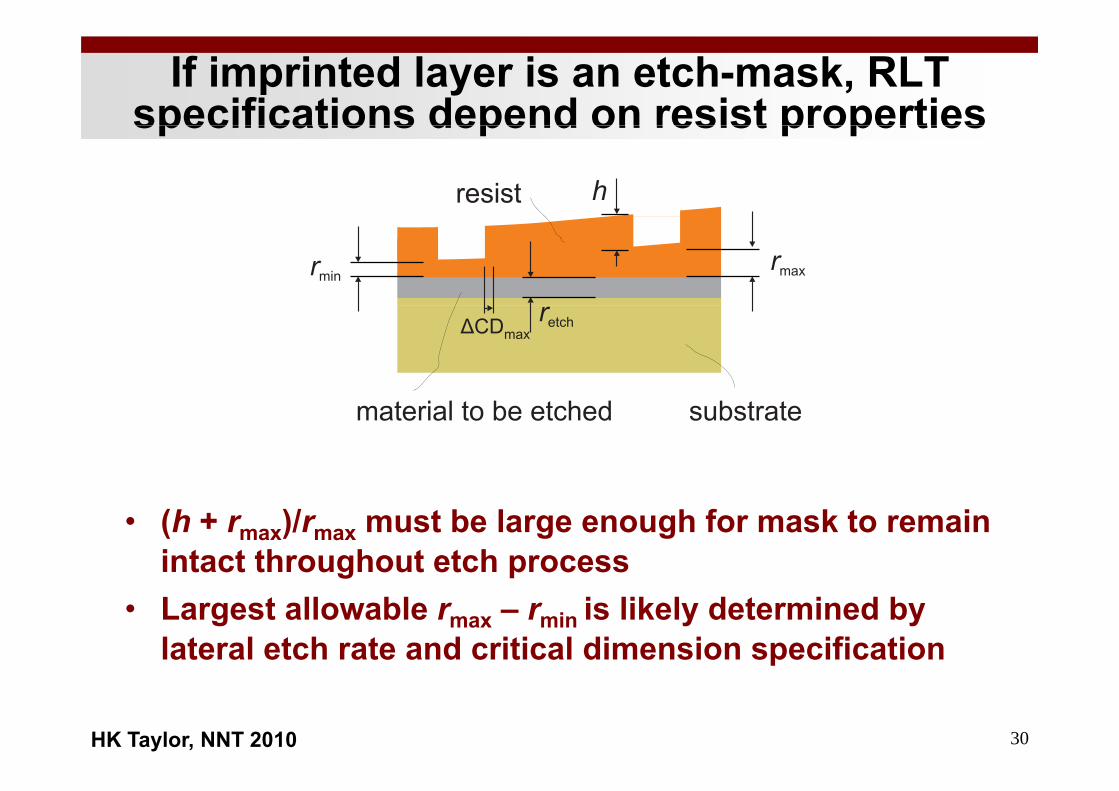
If imprinted layer is an etch-mask, RLT specifications depend on resist propertiesspecifications depend on resist properties
• (h + rmax)/rmax must be large enough for mask to remain intact throughout etch processg p
• Largest allowable rmax – rmin is likely determined by lateral etch rate and critical dimension specification
30
p
HK Taylor, NNT 2010
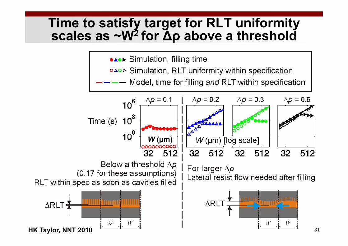
Time to satisfy target for RLT uniformity scales as ~W2 for ∆ρ above a thresholdscales as W for ∆ρ above a threshold
W (µm)
31HK Taylor, NNT 2010
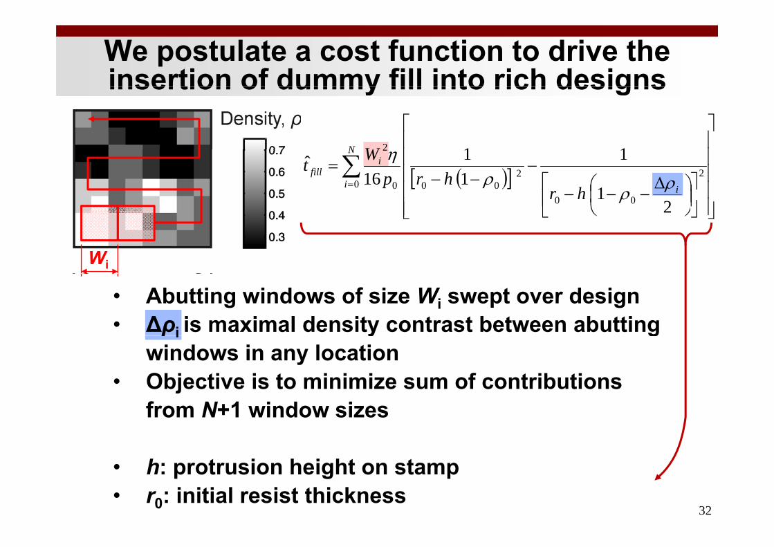
We postulate a cost function to drive the insertion of dummy fill into rich designsinsertion of dummy fill into rich designs
N W 2 11
N
i i
ifill
hrhrp
Wt0
2
00
2000
2
21
111
16ˆ
Wi
2
• Abutting windows of size Wi swept over design• ∆ρi is maximal density contrast between abutting ρi y g
windows in any location• Objective is to minimize sum of contributions
from N+1 window sizes
h t i h i ht t
32
• h: protrusion height on stamp• r0: initial resist thickness
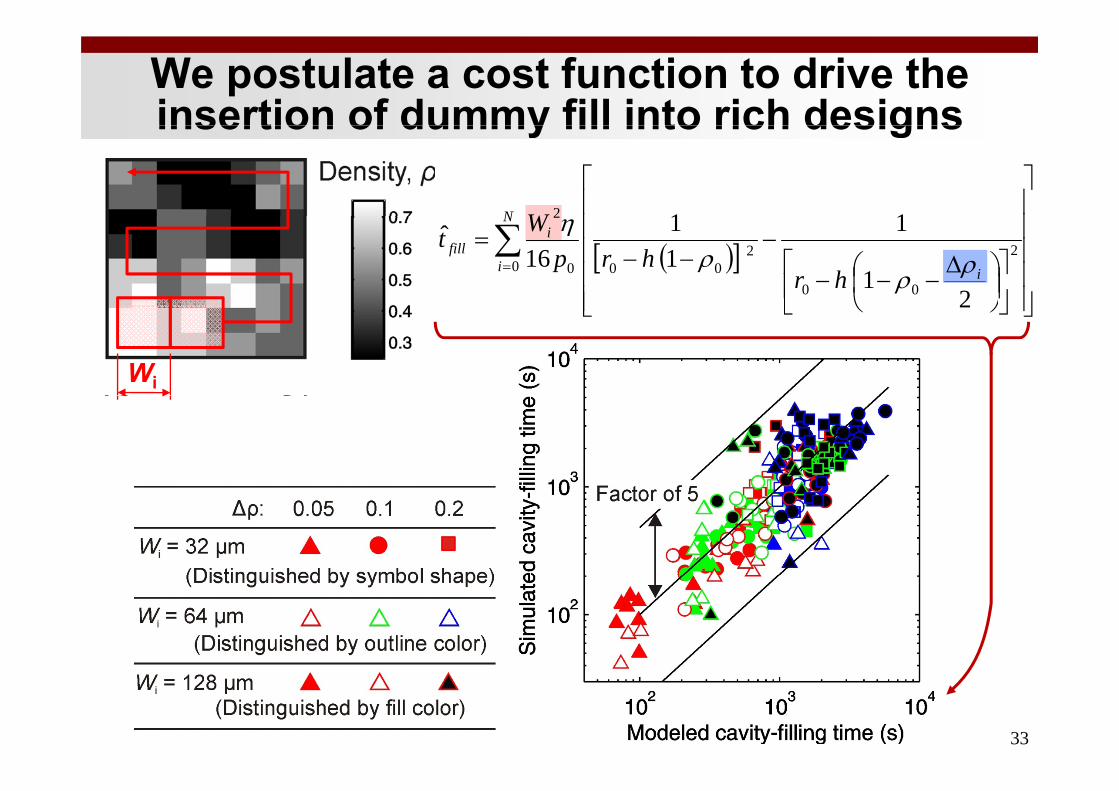
We postulate a cost function to drive the insertion of dummy fill into rich designsinsertion of dummy fill into rich designs
N W 2 11
N
i i
ifill
hrhrp
Wt0
2
00
2000
2
21
111
16ˆ
Wi
2
33
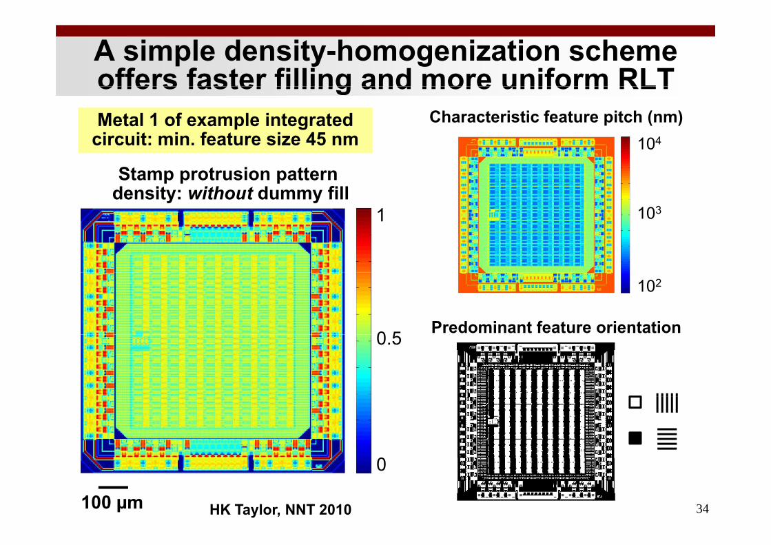
A simple density-homogenization scheme offers faster filling and more uniform RLToffers faster filling and more uniform RLT
Characteristic feature pitch (nm)104
Metal 1 of example integrated circuit: min. feature size 45 nm
1
Stamp protrusion pattern density: without dummy fill
103
10
1 103
0 5
102
Predominant feature orientation0.5
0
34
0
100 µm HK Taylor, NNT 2010
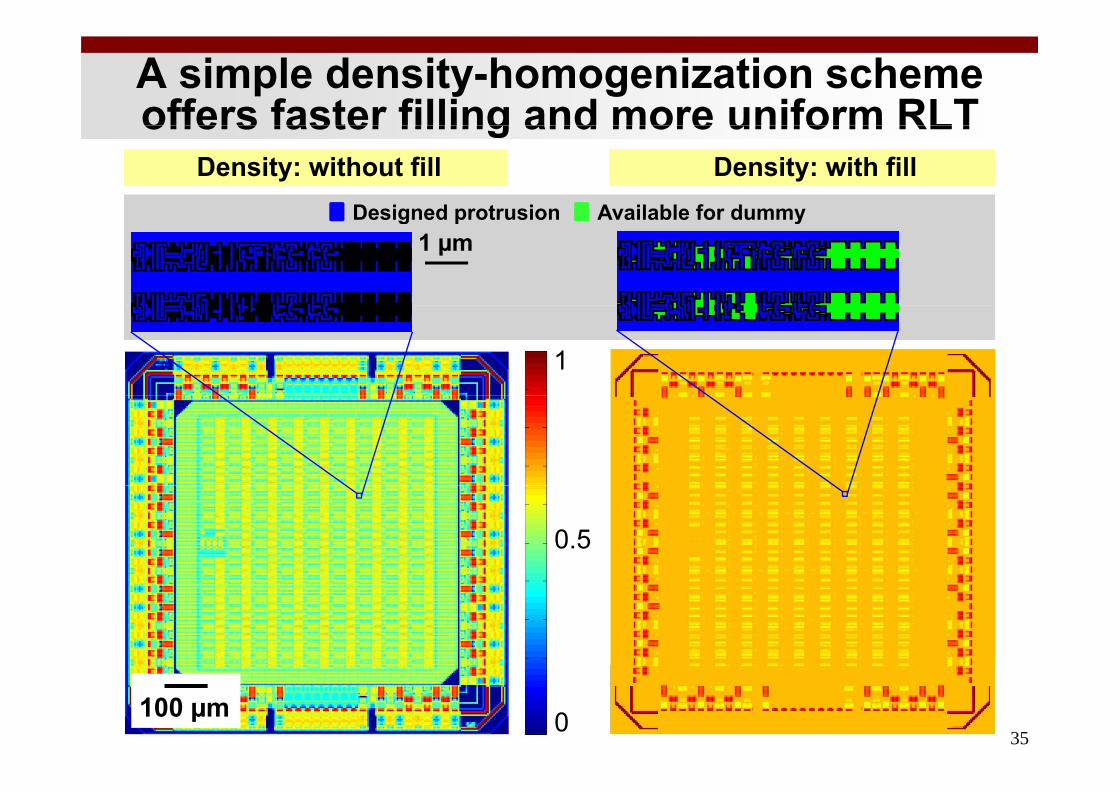
A simple density-homogenization scheme offers faster filling and more uniform RLToffers faster filling and more uniform RLT
Density: without fill Density: with fillDesigned protrusion Available for dummy
1 µmDesigned protrusion Available for dummy
1
0.5
350100 µm
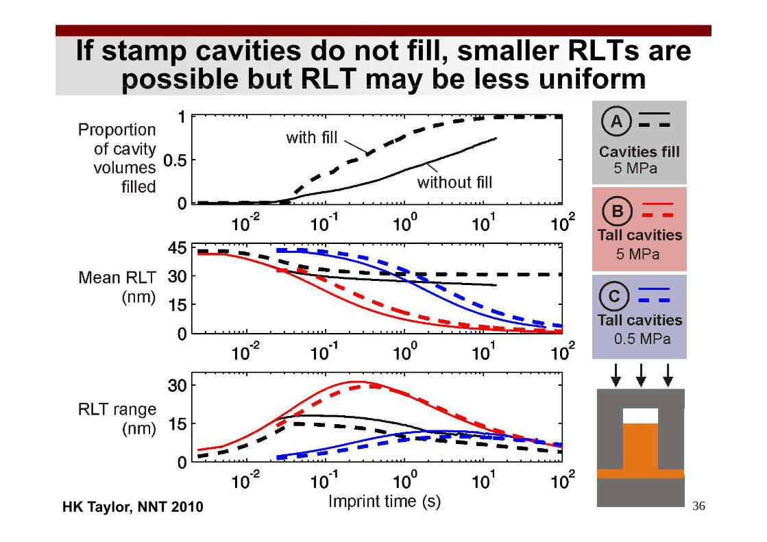
If stamp cavities do not fill, smaller RLTs are possible but RLT may be less uniformpossible but RLT may be less uniform
36HK Taylor, NNT 2010
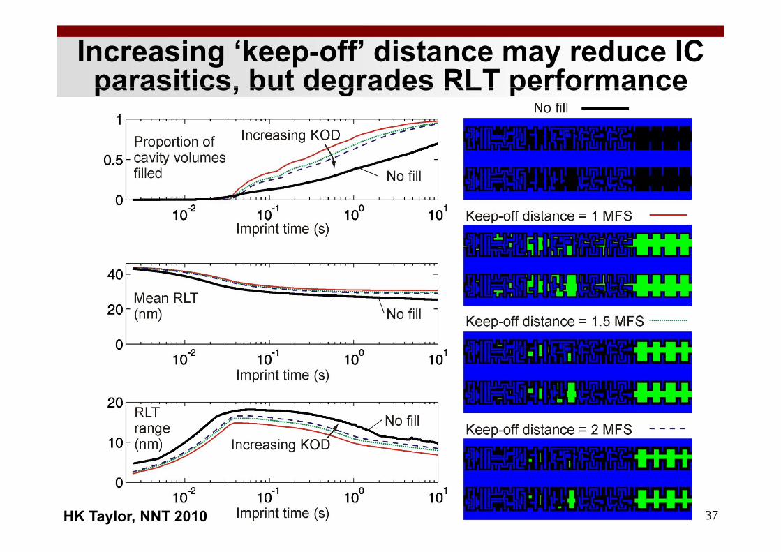
Increasing ‘keep-off’ distance may reduce IC parasitics, but degrades RLT performanceparasitics, but degrades RLT performance
37HK Taylor, NNT 2010
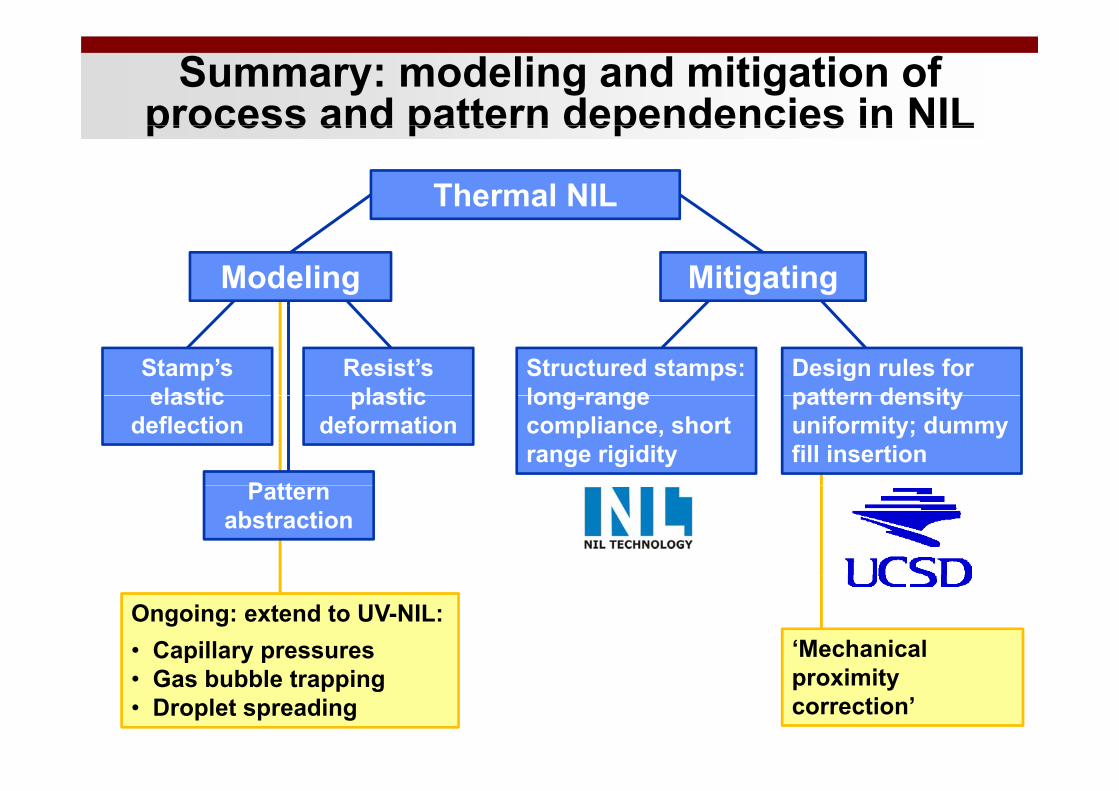
Summary: modeling and mitigation of process and pattern dependencies in NILprocess and pattern dependencies in NIL
Thermal NIL
Modeling Mitigating
Structured stamps: long range
Stamp’s elastic
Resist’splastic
Design rules for pattern densitylong-range
compliance, short range rigidity
elastic deflection
plasticdeformation
P tt
pattern density uniformity; dummy fill insertion
Pattern abstraction
Ongoing: extend to UV-NIL:• Capillary pressures ‘Mechanical • Gas bubble trapping• Droplet spreading
proximity correction’