Embed Size (px)
Citation preview
University of Central Florida University of Central Florida
STARS STARS
Electronic Theses and Dissertations, 2004-2019
2005
Modeling And Simulation Of Long Term Degradation And Lifetime Modeling And Simulation Of Long Term Degradation And Lifetime
Of Deep-submicron Mos Device And Circuit Of Deep-submicron Mos Device And Circuit
Zhi Cui University of Central Florida
Part of the Electrical and Electronics Commons
Find similar works at: https://stars.library.ucf.edu/etd
University of Central Florida Libraries http://library.ucf.edu
This Doctoral Dissertation (Open Access) is brought to you for free and open access by STARS. It has been accepted
for inclusion in Electronic Theses and Dissertations, 2004-2019 by an authorized administrator of STARS. For more
information, please contact [email protected].
STARS Citation STARS Citation Cui, Zhi, "Modeling And Simulation Of Long Term Degradation And Lifetime Of Deep-submicron Mos Device And Circuit" (2005). Electronic Theses and Dissertations, 2004-2019. 300. https://stars.library.ucf.edu/etd/300
MODELING AND SIMULATION OF LONG TERM DEGRADATION AND LIFETIME OF DEEP-SUBMICRON MOS
DEVICE AND CIRCUIT
by
ZHI CUI
A dissertation submitted in partial fulfillment of the requirements for the degree of Doctor of Science
in the Department of Electrical & Computer Engineering in the College of Engineering & Computer Science
at the University of Central Florida Orlando, Florida
Spring Term 2005
Major Professor: Juin. J. Liou
ii
© 2005 Zhi Cui

iii
ABSTRACT
Long-term hot-carrier induced degradation of MOS devices has become more severe as the
device size continues to scale down to submicron range. In our work, a simple yet effective method
has been developed to provide the degradation laws with a better predictability. The method can be
easily augmented into any of the existing degradation laws without requiring additional algorithm.
With more accurate extrapolation method, we present a direct and accurate approach to modeling
empirically the 0.18-μm MOS reliability, which can predict the MOS lifetime as a function of
drain voltage and channel length. With the further study on physical mechanism of MOS device
degradation, experimental results indicated that the widely used power-law model for lifetime
estimation is inaccurate for deep submicron devices. A better lifetime prediction method is
proposed for the deep-submicron devices. We also develop a Spice-like reliability model for
advanced radio frequency RF MOS devices and implement our reliability model into SpectreRF
circuit simulator via Verilog-A HDL (Hardware Description Language). This RF reliability model
can be conveniently used to simulate RF circuit performance degradation

iv
ACKNOWLEDGMENTS
At first, I would like to gratefully acknowledge the enthusiastic supervision of my
professor Dr. J. J. Liou during this work.
I specially thank Dr. Yun Yue for the technical support and discussion.
I thank my dissertation committee for their interest and time: Dr. J.J. Liou, Dr. Kalpathy B.
Sundaram, Dr. Takis C. Kasparis, Dr. Thomas Xinzhang Wu, and Dr. Yun Yue.
I am grateful to all my friends from Micronelectronic Lab: Xiaofang Gao, Ji Chen, Hao
Ding, Yue Fu, Javier Salcedo, Lifang Lou, and Xiang Liou.
Finally, I am forever indebted to my parents and my wife for their understanding, endless
patience and encouragement when it was most required.
v
TABLE OF CONTENTS
ABSTRACT............................................................................................................................... iii LIST OF FIGURES .................................................................................................................. vii LIST OF TABLES.......................................................................................................................x
1. INTRODUCTION ...............................................................................................................1
1.1 Introduction................................................................................................................1
1.2 Hot-Carrier Injection Phenomenon............................................................................2
1.3 Thesis Outline ............................................................................................................4
2. CHARACTERIZATION TECHNIQUES...........................................................................7
2.1 Introduction................................................................................................................7
2.2 Drain Current Characteristics ....................................................................................8
2.3 Channel Transconductance and Mobility ................................................................13
2.4 Stress condictions and Effect of Hot-Carrier Injection on MOS devices ................14
2.5 Conclusion ...............................................................................................................15
3. A NEW EXTRAPOLATION METHOD FOR LONG-TERM DEGRADATION PREDICTION OF DEEP-SUBMICRON MOSFETs .......................................................16
3.1 Degradation Law......................................................................................................16
3.2 New extrapolation method.......................................................................................17
3.3 MOS data analysis and degradation prediction .......................................................18
3.4 Conclusion ...............................................................................................................27
4. EMPIRICAL RELIABILITY MODELING FOR 0.18 μm MOS DEVICES ...................28
4.1 Introduction..............................................................................................................28
4.2 Measurement procedure...........................................................................................29
4.3 Empirical model development .................................................................................32
4.4 Conclusion ...............................................................................................................40
5. SUBSTRATE CURRENT, GATE CURRENT, GATE CURRENT AND LIFETIME PREDICTION OF DEEP-SUBMICRON nMOS DEVICES............................................41
5.1 Introduction..............................................................................................................41
5.2 Experiments .............................................................................................................42
5.3 Substrate current, gate current, and lifetime estimation ..........................................43
5.3.1 Substrate current and gate current in deep-submicron devices.................43
5.3.2 New lifetime estimation model.................................................................51
vi
5.4 Discussions ..............................................................................................................55
5.5 Conclusion ...............................................................................................................56
6. A SPICE-LIKE RELIABILITY MODEL FOR DEEP-SUBMICRON CMOS TECHNOLOGY ................................................................................................................58
6.1 Introduction..............................................................................................................58
6.2 Methodology............................................................................................................58
6.3 Lifetime determination.............................................................................................60
6.4 Reliability model development ................................................................................63
6.5 Prediction of DC and RF performance degradation ................................................73
6.6 Conclusion ...............................................................................................................75
APPENDIX: VERILOG-A CODE............................................................................................76
REFERENCES ........................................................................................................................141
vii
LIST OF FIGURES
Figure 1 Hot carrier generation in nMOS devices. ................................................................. 3
Figure 2 Energy band diagram showing the barrier heights for injection of electron and holes from Si to SiO2.......................................................................................................... 4
Figure 3 The device terminals used to measure mode parameters relative to the terminals used during hot-carrier stressing experiments................................................................... 9
Figure 4 Linear threshold voltage extraction from plot of IDS vs VGS................................... 10
Figure 5 Saturation threshold voltage extraction from plot of IDS vs VGS ............................ 11
Figure 6 The IDS-VDS characteristics measured before and after a typical hot-carrier stress in n-channel MOSFETs. ............................................................................................. 12
Figure 7 The IDS-VGS characteristics measured before and after a typical hot-carrier stress in n-channel MOSFETs. ............................................................................................. 13
Figure 8 transconductance and mobility extraction from plot of IDS vs VGS ..................... 14
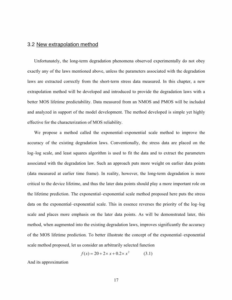
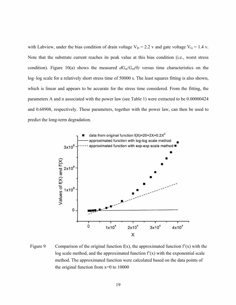
Figure 9 Comparison of the original function f(x), the approximated function f’(x) with the log scale method, and the approximated function f’(x) with the exponential scale method. The approximated function were calculated based on the data points of the original function from x=0 to 10000....................................................................... 19
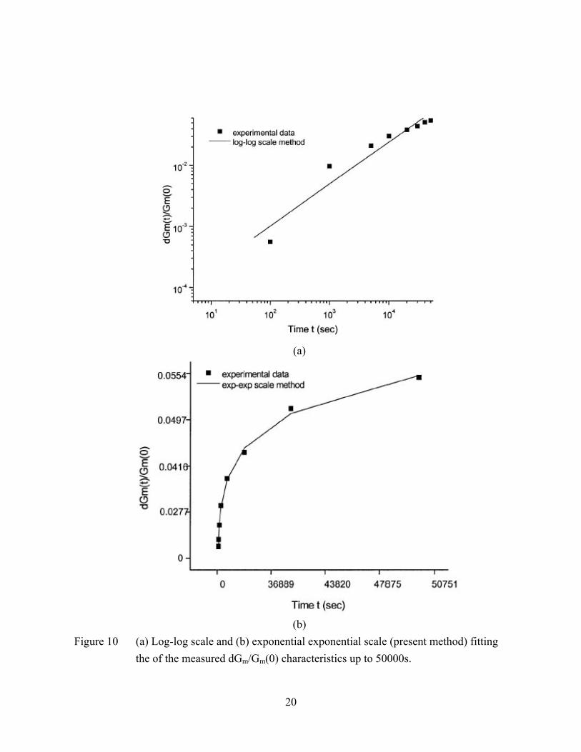
Figure 10 (a) Log-log scale and (b) exponential exponential scale (present method) fitting the of the measured dGm/Gm(0) characteristics up to 50000s....................................... 20
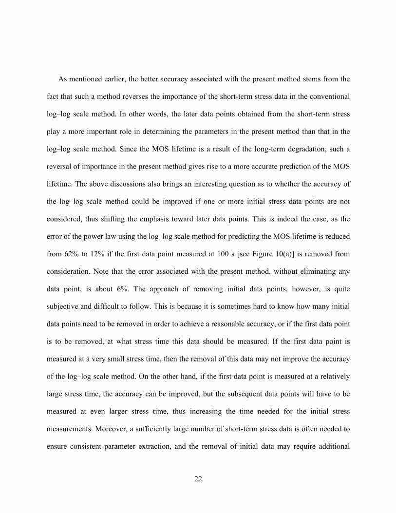
Figure 11 Comparison of dGm/Gm(0) characteristics of a 0.18-μm NMOS up to 250000 s measured and predicted from the power law, saturation law, and the two laws with the present exponential-exponential method based on the short-term stress data (stress time of 50000s). ........................................................................................... 24
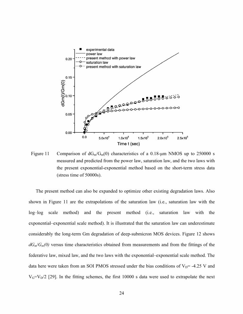
Figure 12 Comparison of dGm/Gm(0) characteristics of an SOI PMOS [6] up to 50000 s measured and predicted from the fedrative law, and the two laws with the present exponential method based on the short-term stress data ( stress time of 10000 s). 26
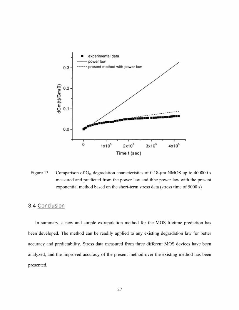
Figure 13 Comparison of Gm degradation characteristics of 0.18-μm NMOS up to 400000 s measured and predicted from the power law and thhe power law with the present exponential method based on the short-term stress data (stress time of 5000 s) .... 27
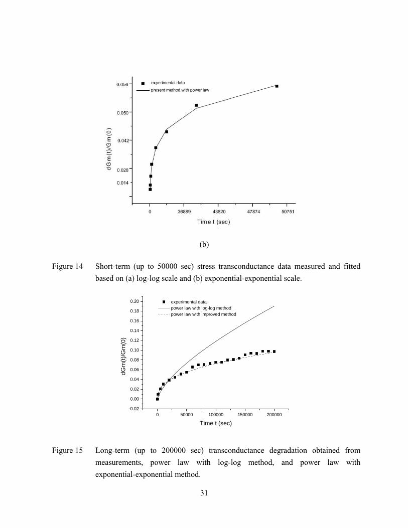
Figure 14 Short-term (up to 50000 sec) stress transconductance data measured and fitted based on (a) log-log scale and (b) exponential-exponential scale. ................................... 31
viii
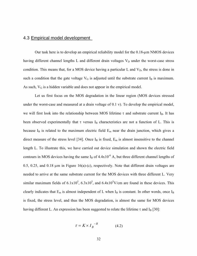
Figure 15 Long-term (up to 200000 sec) transconductance degradation obtained from measurements, power law with log-log method, and power law with exponential-exponential method............................................................................. 31
Figure 16 Electric field contours obtained from device simulation for MOS devices having three different channel length of 0.5, 0.25, and 0.18 μm but the same substrate current of 4.4x10⁻⁶ A. The maximum fields in the three devices are also indicated.................................................................................................................................. 37
Figure 17 Lifetime versus substrate current obtained from measurements and fitting. .......... 37
Figure 18 Substrate current versus 1/VD for three different channel lengths obtained from measurements and fitting. ....................................................................................... 38
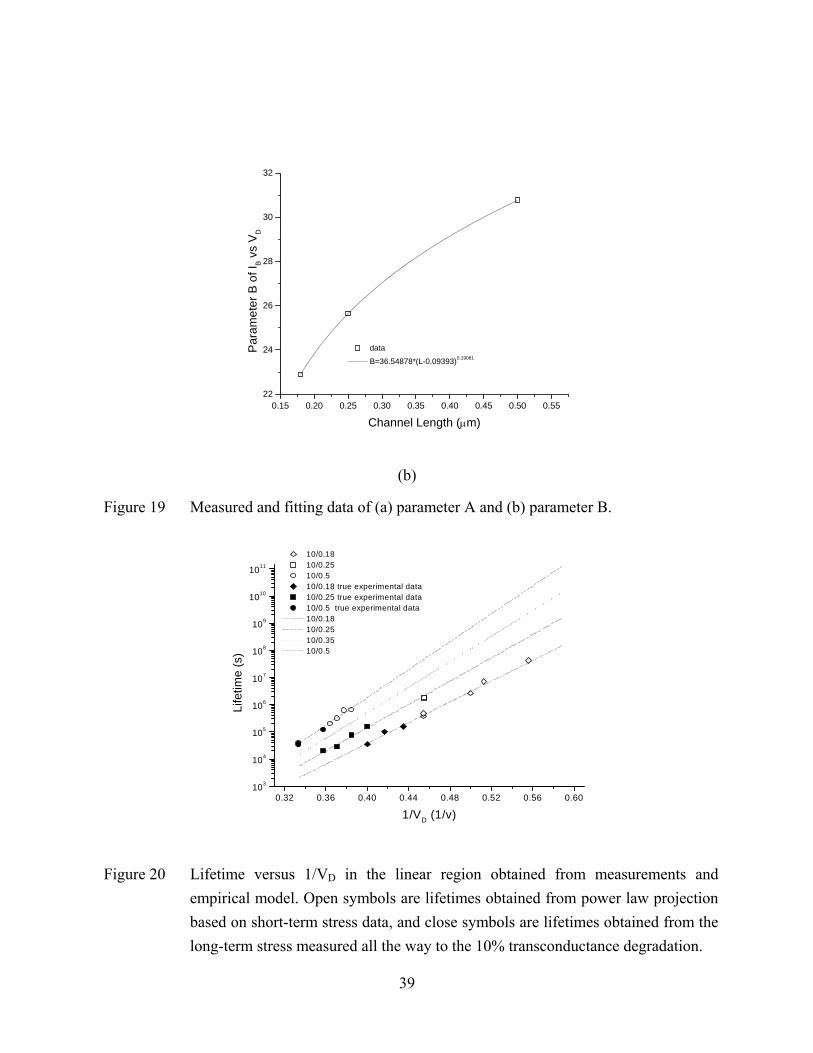
Figure 19 Measured and fitting data of (a) parameter A and (b) parameter B........................ 39
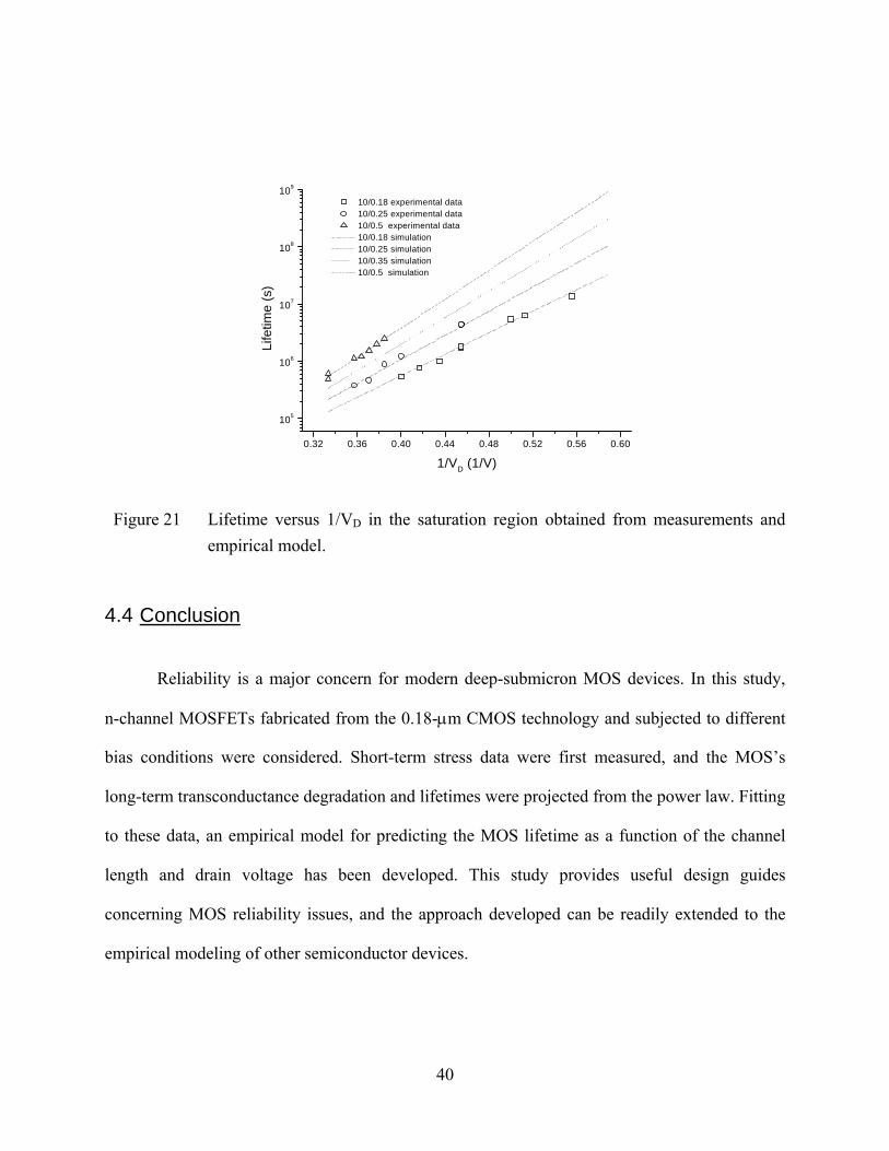
Figure 20 Lifetime versus 1/VD in the linear region obtained from measurements and empirical model. Open symbols are lifetimes obtained from power law projection based on short-term stress data, and close symbols are lifetimes obtained from the long-term stress measured all the way to the 10% transconductance degradation.................. 39
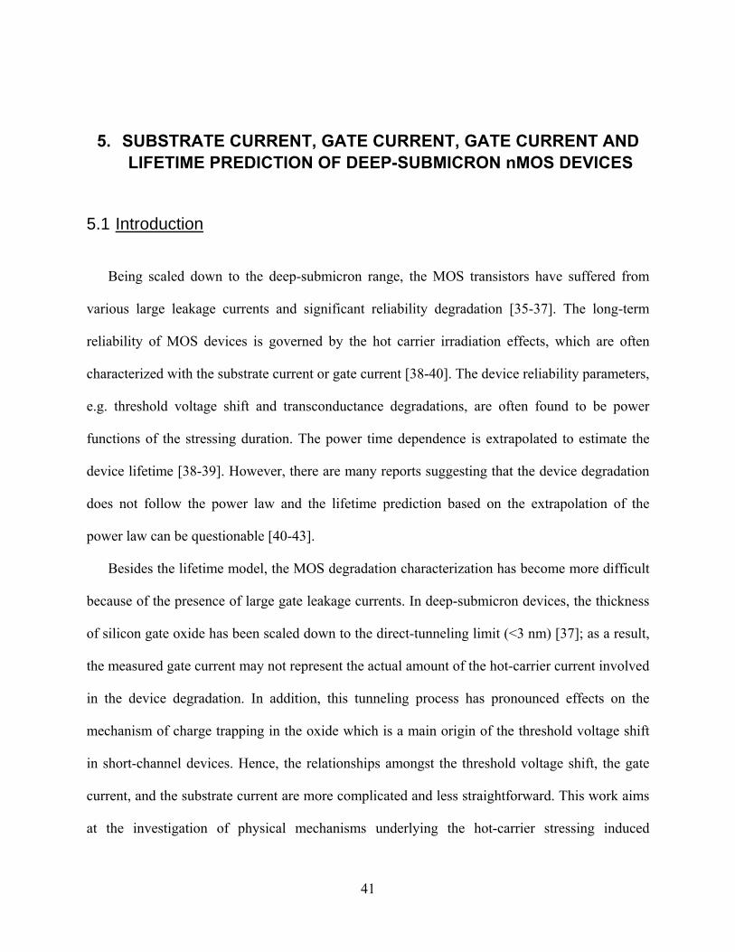
Figure 21 Lifetime versus 1/VD in the saturation region obtained from measurements and empirical model. ..................................................................................................... 40
Figure 22 (a) Substrate current vs. gate voltage characteristics (b) drain current, substrate current and gate current vs. drain voltage characteristics under the worst-case stress condition (i.e., maximum substrate current) ........................................................... 45
Figure 23 Power-law fitting of 0.18 μm and 0.25 μm MOS devices. Markers are the experimental data and lines are the curve fittings using the power law of ID=A(ISub/ID)-n. ........................................................................................................ 45
Figure 24 Power-law fitting of 0.18 μm and 0.25 μm MOS devices. Markers are the experimental data and lines are the curve fittings using the power law of ID=A(ISub/ID)-n. ........................................................................................................ 46
Figure 25 Plot of lifetime as a function of gate current for devices with channel length of 0.18, 0.25 and 0.5 μm. Markers are the experimental data and lines are curve fittings. The values of fitting parameters for each device are listed in the table. Good power law fittings are obtained but large variations of the model parameters suggested the fittings are impractical. ........................................................................................... 47
Figure 26 Generation of substrate and gate currents in long-channel MOS devices. Solid lines indicate the major current or charge transport and dash lines indicate charge transport may exist but are negligible. Modified based on Ref. [49]. .................... 49
ix
Figure 27 Generation of substrate and gate currents in deep submicron MOS devices. Solid lines indicate the major current or charge transport and dash lines indicate charge transport may exist but are negligible. Modified based on Ref. [49]. .................... 50
Figure 28 Plot of lifetime as a function of gate/substrate current ratio for MOS transistor with 0.18 μm gate length. Markers are experimental data and lines are exponential fitting using Eq. (5.2). Table inserted lists the values of fitting parameters...................... 53
Figure 29 Relationship between threshold voltage shift and transconductance degradation measured for MOS devices having three different channel lengths. ...................... 53
Figure 30 Exponential fit of transconductance lifetime with the gate current/substrate current ratio for deep submicron devices. The lifetime represents the duration for making 10% transconduactance degradation at the substrate current. Markers are experimental data and lines are exponential fitting using Eq. (5.2)........................ 54
Figure 31 A methodology of RF circuits performance degradation making use of reliability simulation................................................................................................................ 59
Figure 32 Transconductance lifetime versus substrate current obtained from measurements and fitting....................................................................................................................... 62
Figure 33 Threshold voltage lifetime versus substrate current obtained from measurements and fitting....................................................................................................................... 62
Figure 34 Comparison of threshold voltage VT extracted from IDS vs VDS using equation 6.6 with simulation VT from BSIM 3v3 model ............................................................ 65
Figure 35 Extraction of coefficient A and n from time dependent VT shift............................ 66
Figure 36 Fitting data of VT coefficient A at different substrate current ISUB......................... 67
Figure 37 Fitting data of VT coefficient n at different substrate current ISUB.......................... 67
Figure 38 Comparison of mobility U0 extracted from Gm vs VG using equation 6.9 with simulation U0 from BSIM 3v3 model. ................................................................... 69
Figure 39 Extraction of coefficient A and n from time dependent U0 shift. .......................... 70
Figure 40 Fitting data of U0 coefficient A at different substrate current ISUB. ....................... 70
Figure 41 Fitting data of U0 coefficient n at different substrate current ISUB. ........................ 71
Figure 42 Our degradation MOS BSIM 3 model Verilog-A code (a) and the schematic in Cadence SPECTRE (b) ........................................................................................... 73
Figure 43 Comparison simulation results and measured data for fresh device and stressed after 3000s and 10000s.................................................................................................... 74
Figure 44 Comparison simulation results and measured data for fresh device and stressed after 3000s and 10000s.................................................................................................... 74
x
LIST OF TABLES
Table 1 Expressions of the four different degradation laws, where Y(t) is the time dependent variable y(0)=Y(t=0), and parameters A, n, and B are to be extracted from the measured data.......................................................................................................... 16
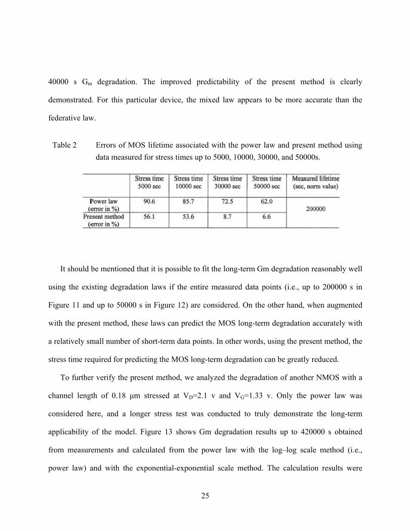
Table 2 Errors of MOS lifetime associated with the power law and present method using data measured for stress times up to 5000, 10000, 30000, and 50000s.......................... 25
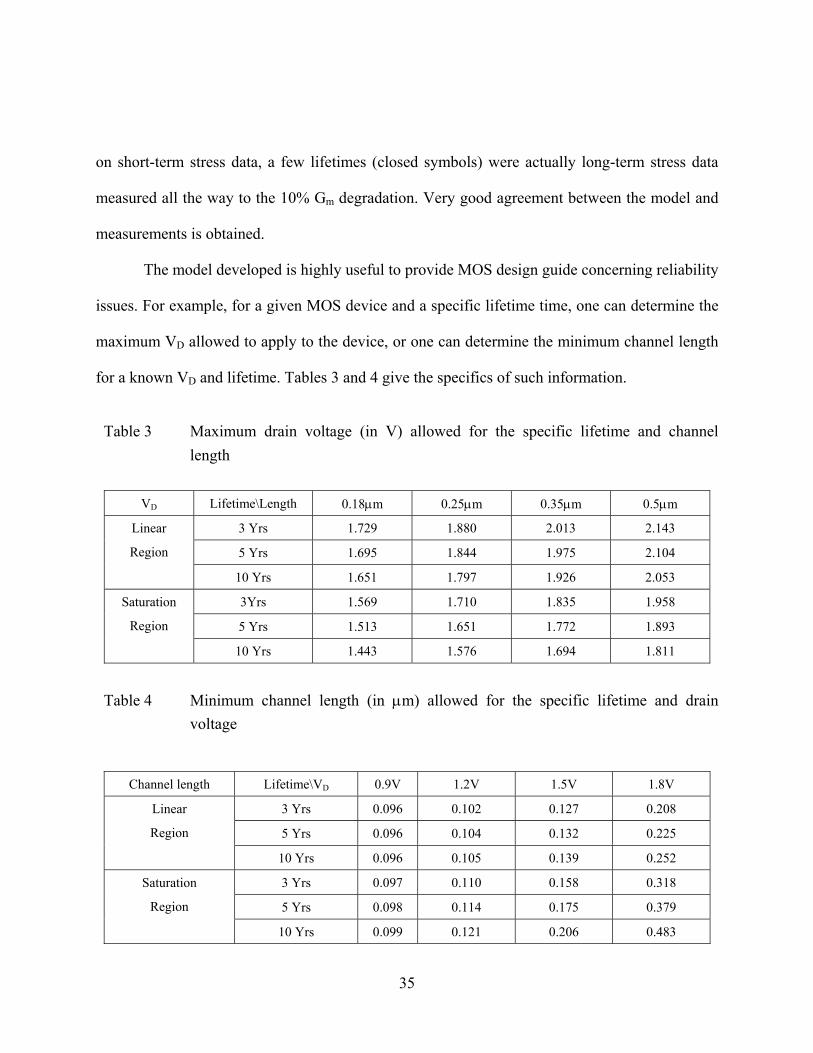
Table 3 Maximum drain voltage (in V) allowed for the specific lifetime and channel length................................................................................................................................. 35
Table 4 Minimum channel length (in μm) allowed for the specific lifetime and drain voltage................................................................................................................................. 35
Table 5 The influence of BSIM DC parameters on single MOS circuit performance......... 63
Table 6 The influence of BSIM RF parameters on single MOS circuit performance ......... 64
1
1. INTRODUCTION
1.1 Introduction
Lilienfeld and Heil conceived the insulated-gate field-effect transistor in the 1930s. An
insulated-gate transistor is distinguished by the presence of an insulator between the main control
terminal and the remainder of the device. Ideally, the transistor draws no current through its gate.
This is sharp contrast to bipolar junction transistors that require a significant base current to
operate. Unfortunately, the Metal-Oxide-Semiconductor Field-Effect Transistor (MOSFET) had
to wait nearly 30 years until the 1960s when manufacturing advances made the device a practical
reality. Since then, the explosive growth of MOSFETs in electronics became ever more prevalent
when “complementary” types of MOSFET devices were combined by Wanlass in the early
1960s to produce logic that required virtually no power except when changing state. MOSFET
processes that offer complementary types of transistors are known as Complementary Metal
Oxide Semiconductor (CMOS) processes, and are the foundation of the modern commodity
electronics industry.
The dimensions of metal-oxide-silicon field effect transistors (MOSFETs) have been
decreasing due to the continuous demand for higher packing densities and faster circuit speeds.
Hot-carrier induced degradation of MOS devices has become more severe as the device size
continues to scale down below 0.1 μm. As a consequence, the degree of reliability concern is
increased when advanced MOSFETs are used in modern electronics systems.
2
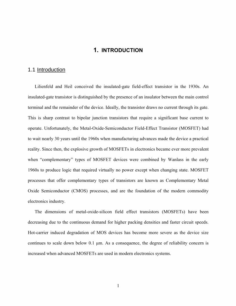
1.2 Hot-Carrier Injection Phenomenon
A brief overview of the hot-carrier injection phenomenon and the resulting device
degradation will be provided in this section. The cross-section of a typical n-channel MOSFET
operating in saturation is shown in Figure 1. The large voltage drop across the pinch-off region
results in a high lateral electric field close to the drain region. The carriers traversing this high
field region reach energies, which are considerably higher than the equilibrium thermal energy in
the semiconductor lattice. These high-energy carriers are called hot-carriers. Hot-carriers with
energies above the impact-ionization threshold (1.6eV) [2] can generate electron-hole pairs in
this region through impact-ionization. Some of these carriers, with energies large enough to
overcome the potential barrier between Si and SiO2 and their momentum directed towards the
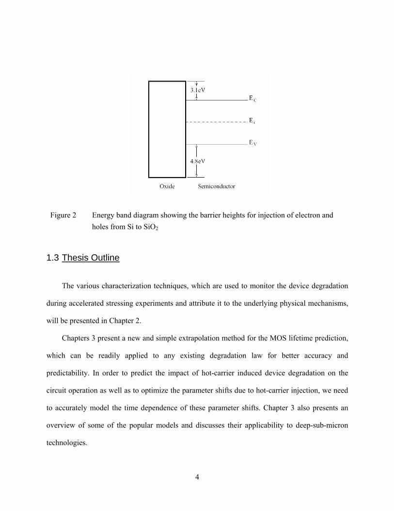
Si-SiO2 interface, can get injected into the gate oxide [4]. As shown in Figure 2, the energy
barrier for injection of electrons (3.1eV) is considerably smaller than that for holes (4.8eV)
making hole-injection a less probable event as compared to electron-injection. The exact barrier
at any given point along the channel is affected by the transverse electric field at that point due to
the Schottky effect [3]. A large proportion of the injected electrons reaches the gate terminal and
contributes to the gate current. However, some of the injected electrons can also get trapped at
certain defects present in the gate oxide [5, 6]. Similarly, the injected holes can reach the gate
and contribute to the gate current. However, as the hole mobility in SiO2 is considerably smaller
than that of electrons [7], holes have a higher probability of getting trapped. In addition to getting
trapped in the gate-oxide, the injected carriers can also result in increase in the density of
interface traps present at the Si-SiO2 interface [8, 9, 10]. The presence of charge in the
gate-oxide and at the Si-SiO2 interface of a MOSFET results in modulation of the surface
3
potential and carrier mobility at the surface of the semiconductor. These phenomena alter the
device current characteristics, which can significantly reduce the operating lifetime of these
devices [11].
As mentioned earlier, the injection of carriers into the gate-oxide is a significant concern for
assuring the long-term reliability of modern digital CMOS circuits. As these degradation
processes are relatively slow during circuit operation, in order to characterize the hot-carrier
response of devices within short times they are often subjected to much larger biases than those
present in real circuits. The presence of higher biases results in acceleration of the degradation
processes and hence such experiments are called accelerated stressing experiments. The
extrapolation of the results obtained from the accelerated stressing experiments to real-life circuit
operation is a subject of other chapters later in this dissertation.
Figure 1 Hot carrier generation in nMOS devices.
4
Figure 2 Energy band diagram showing the barrier heights for injection of electron and holes from Si to SiO2
1.3 Thesis Outline
The various characterization techniques, which are used to monitor the device degradation
during accelerated stressing experiments and attribute it to the underlying physical mechanisms,
will be presented in Chapter 2.
Chapters 3 present a new and simple extrapolation method for the MOS lifetime prediction,
which can be readily applied to any existing degradation law for better accuracy and
predictability. In order to predict the impact of hot-carrier induced device degradation on the
circuit operation as well as to optimize the parameter shifts due to hot-carrier injection, we need
to accurately model the time dependence of these parameter shifts. Chapter 3 also presents an
overview of some of the popular models and discusses their applicability to deep-sub-micron
technologies.
5
Basing on extrapolation method in Chapter 3, we present a simple yet effective approach to
modeling the 0.18-μm MOS reliability empirically. Short-term stress data are first measured, and
the well-known power law is used to project the MOS long-term degradation and lifetime. These
results are then used as the basis for the development of an empirical model to predict the MOS
lifetime as a function of drain voltage and channel length. The study focuses on the worst-case
stress condition, and both the linear and saturation operations are considered in the modeling.
The approach developed has useful applications to the empirical modeling of MOS and other
semiconductor devices. This study provides useful design guides concerning MOS reliability
issues, and the approach developed can be readily extended to the empirical modeling of other
semiconductor devices. This work will be presented in Chapter 4. As a part of this work, a set of
stressing experiments is suggested to study the various aspects of device degradation in
n-channel MOSFETs comprehensively.
With deep study on submicron MOSFETs, experimental results are presented to indicate
that the widely used power-law models for lifetime estimation are questionable for deep
submicron (< 0.25 μm) MOS devices, particularly for the case of large substrate current stressing.
This observation is attributed to the presence of current components, such as the gate tunneling
current and base current of parasitic bipolar transistor, that do not induce device degradation. A
more effective extrapolation method is proposed as an alternative for the reliability
characterization of deep-submicron MOS devices. Chapter 5 is focus on a more effective
extrapolation method for the reliability characterization of deep-submicron MOS devices. This
method will account into the effect of gate tunneling current and base current of parasitic bipolar
transistor that do not induce device degradation. A simple and accurate empirical expression
6
correlating the MOS lifetime with the ratio of gate to substrate current has been proposed in this
chapter. This model also gives better physical insights than the existing power-law models.
In the final part of the thesis, we found the conventional modeling for hot-carrier aging is
questionable for deep-submicron devices, and a systematic method is needed for predicting the
lifetime of the devices and circuits. In this chapter, we develop a Spice-like reliability model for
advanced radio frequency RF MOS devices and implement the model into SpectreRF circuit
simulator via Verilog-A HDL (Hardware Description Language).
7
2. CHARACTERIZATION TECHNIQUES
2.1 Introduction
The injection of hot-carriers into the gate-oxide of MOSFETs triggers carrier trapping and
interface trap generation processes. The presence of interfacial and bulk charge in the gate-oxide
affects the DC current characteristics and AC properties of these devices. The alteration of the
current characteristics effectively results in variations in some of the parameters extracted from
them such as the threshold voltage, subthreshold slope and the transconductance [11, 12, 13].
These parameter shifts can be used as measures of the degradation as well as a key to understand
the underlying physical mechanisms. The drain current characteristics (IDS-VGS and IDS-VDS) can
be utilized to provide accurate information about the degradation processes when the hot-carriers
are injected uniformly along the channel of the device, such as during substrate hot-carrier
injection experiments [14, 15]. For example, the variations in the IDS vs VGS characteristic
measured in saturation can be used to obtain the contributions due to interface traps and fixed
charge in the oxide using techniques such as the midgap method [16]. These techniques assume
that the change in subthreshold slope is entirely due to interface traps under uniform injection
conditions, it can be assumed that the threshold voltage at each point along the channel of the
device shifts by the same amount. The threshold voltage of the complete device is equivalent to
that of any point along the channel under this condition.
At the same time, it is sometimes possible to explain the observed degradation under
non-uniform carrier injection by different combinations and spatial distributions of interface trap
density and fixed oxide charge [17]. Due to the limitations in the correct interpretation of the
8
variations in drain-current characteristics, certain other characterization techniques, such as charge
pumping and substrate current characteristics, have been used in the some literature. Some of the
most commonly used device characterization techniques which are used to monitor and understand
the device degradation under channel hot-carrier injection will be described in this chapter.
2.2 Drain Current Characteristics
The drain current characteristics as a function of the drain bias as well as the gate bias have
been used extensively in literature to extract parameters, which can be used as degradation
monitors. The commonly used parameters include VT, Gm and IDS. The physical meaning of each
of these parameters can be defined on the basis of a simplified theory of operation of MOSFETs
[3].While performing experiments, the drain current characteristics are obtained in terms of
two-dimensional arrays of numbers. The above parameters need to be extracted numerically from
these data and the extracted values may not directly correlate to the physical definitions of these
parameters.
Each of the above parameters, for example, can be measured from drain current
characteristics obtained in either linear or saturation regions of operation. The two most important
parameters, which are extracted numerically from measured data, are the threshold voltage and the
channel transconductance. The definitions of these parameters and the techniques used to extract
them numerically from measured data will be presented.
9
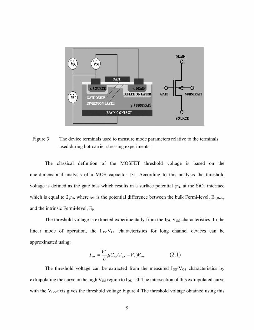
Figure 3 The device terminals used to measure mode parameters relative to the terminals
used during hot-carrier stressing experiments.
The classical definition of the MOSFET threshold voltage is based on the
one-dimensional analysis of a MOS capacitor [3]. According to this analysis the threshold
voltage is defined as the gate bias which results in a surface potential ψB, at the SiO2 interface
which is equal to 2ψB, where ψB is the potential difference between the bulk Fermi-level, EF,Bulk,
and the intrinsic Fermi-level, Ei.
The threshold voltage is extracted experimentally from the IDS-VGS characteristics. In the
linear mode of operation, the IDS-VGS characteristics for long channel devices can be
approximated using:
DSTGSoxDS VVVCL
WI )( −= μ (2.1)
The threshold voltage can be extracted from the measured IDS-VGS characteristics by
extrapolating the curve in the high VGS region to IDS = 0. The intersection of this extrapolated curve
with the VGS-axis gives the threshold voltage Figure 4 The threshold voltage obtained using this
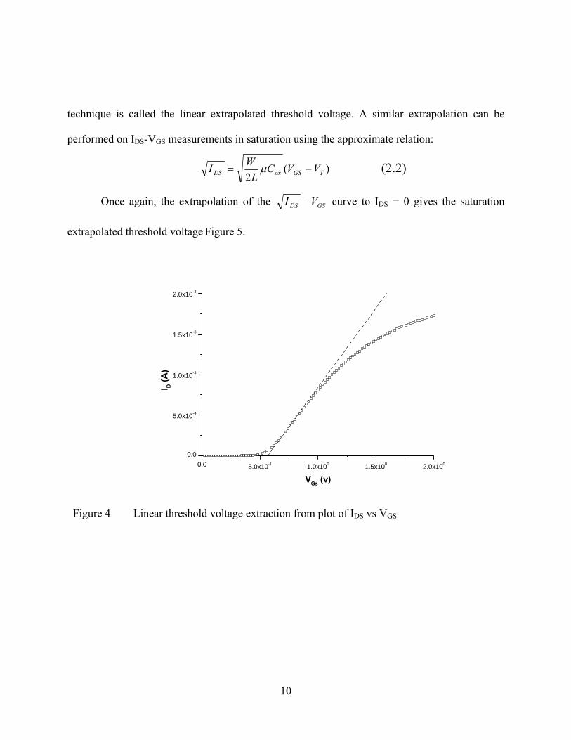
10
technique is called the linear extrapolated threshold voltage. A similar extrapolation can be
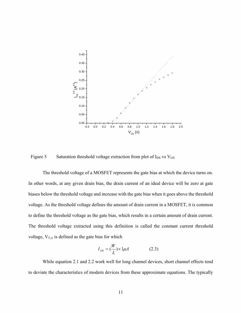
performed on IDS-VGS measurements in saturation using the approximate relation:
)(2 TGSoxDS VVC
LWI −= μ (2.2)
Once again, the extrapolation of the GSDS VI − curve to IDS = 0 gives the saturation
extrapolated threshold voltage Figure 5.
0.0 5.0x10⁻¹ 1.0x100 1.5x100 2.0x100
0.0
5.0x10⁻⁴
1.0x10⁻³
1.5x10⁻³
2.0x10⁻³
I D (A
)
VGs (v)
Figure 4 Linear threshold voltage extraction from plot of IDS vs VGS
11
-0.2 0.0 0.2 0.4 0.6 0.8 1.0 1.2 1.4 1.6 1.8 2.00.00
0.05
0.10
0.15
0.20
0.25
0.30
0.35
0.40
I DS0.
5 (A0.
5 )
VGS (v)
Figure 5 Saturation threshold voltage extraction from plot of IDS vs VGS
The threshold voltage of a MOSFET represents the gate bias at which the device turns on.
In other words, at any given drain bias, the drain current of an ideal device will be zero at gate
biases below the threshold voltage and increase with the gate bias when it goes above the threshold
voltage. As the threshold voltage defines the amount of drain current in a MOSFET, it is common
to define the threshold voltage as the gate bias, which results in a certain amount of drain current.
The threshold voltage extracted using this definition is called the constant current threshold
voltage, VT,ci is defined as the gate bias for which
AL
WI DS μ1)( ×= (2.3)
While equation 2.1 and 2.2 work well for long channel devices, short channel effects tend
to deviate the characteristics of modern devices from these approximate equations. The typically
12
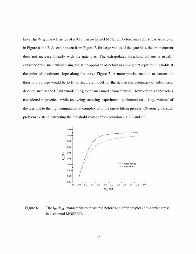
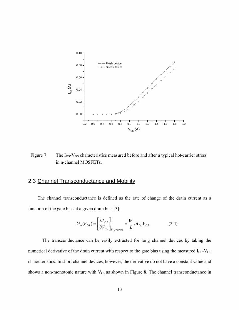
linear IDS-VGS characteristics of a 0.18 μm n-channel MOSFET before and after stress are shown
in Figure 6 and 7. As can be seen from Figure 7, for large values of the gate bias, the drain current
does not increase linearly with the gate bias. The extrapolated threshold voltage is usually
extracted from such curves using the same approach as before assuming that equation 2.1 holds at
the point of maximum slope along the curve Figure 7. A more precise method to extract the
threshold voltage would be to fit an accurate model for the device characteristics of sub-micron
devices, such as the BSIM3 model [18], to the measured characteristics. However, this approach is
considered impractical while analyzing stressing experiments performed on a large volume of
devices due to the high computational complexity of the curve fitting process. Obviously, no such
problem exists in extracting the threshold voltage from equation 2.1 2.2 and 2.3.,
-0.2 0.0 0.2 0.4 0.6 0.8 1.0 1.2 1.4 1.6 1.8 2.0-0.01
0.00
0.01
0.02
0.03
0.04
0.05
0.06
0.07
0.08
Fresh device After stress
I DS (
A)
VGS (A)
Figure 6 The IDS-VDS characteristics measured before and after a typical hot-carrier stress
in n-channel MOSFETs.
13
-0.2 0.0 0.2 0.4 0.6 0.8 1.0 1.2 1.4 1.6 1.8 2.0
0.00
0.02
0.04
0.06
0.08
0.10
Fresh device Stress device
I DS (
A)
VGS (A)
Figure 7 The IDS-VGS characteristics measured before and after a typical hot-carrier stress
in n-channel MOSFETs.
2.3 Channel Transconductance and Mobility
The channel transconductance is defined as the rate of change of the drain current as a
function of the gate bias at a given drain bias [3]:
DSoxconstVGS
DSDSm VC
LW
VIVG
DS
μ=⎥⎦
⎤⎢⎣
⎡∂∂
==
)( (2.4)
The transconductance can be easily extracted for long channel devices by taking the
numerical derivative of the drain current with respect to the gate bias using the measured IDS-VGS
characteristics. In short channel devices, however, the derivative do not have a constant value and
shows a non-monotonic nature with VGS as shown in Figure 8. The channel transconductance in
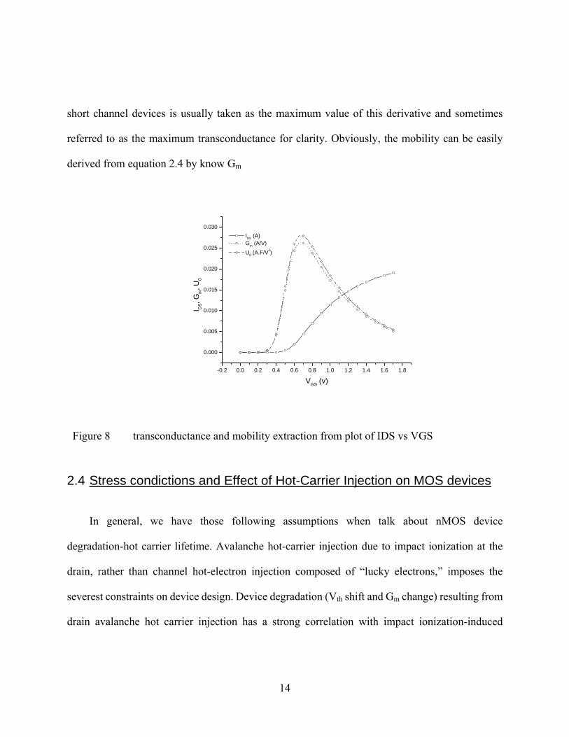
14
short channel devices is usually taken as the maximum value of this derivative and sometimes
referred to as the maximum transconductance for clarity. Obviously, the mobility can be easily
derived from equation 2.4 by know Gm
-0.2 0.0 0.2 0.4 0.6 0.8 1.0 1.2 1.4 1.6 1.8
0.000
0.005
0.010
0.015
0.020
0.025
0.030 IDS (A) Gm (A/V) U0 (A.F/V2)
I DS,
Gm, U
0
VGS (v)
Figure 8 transconductance and mobility extraction from plot of IDS vs VGS
2.4 Stress condictions and Effect of Hot-Carrier Injection on MOS devices
In general, we have those following assumptions when talk about nMOS device
degradation-hot carrier lifetime. Avalanche hot-carrier injection due to impact ionization at the
drain, rather than channel hot-electron injection composed of “lucky electrons,” imposes the
severest constraints on device design. Device degradation (Vth shift and Gm change) resulting from
drain avalanche hot carrier injection has a strong correlation with impact ionization-induced
15
substrate current, ISUB. That is, the gate bias condition which caused the largest degradation which
yields the peak substrate current [19-23].
In our experiment, we chose VGS at maxium ISUB substrate current as our stress conditions,
which can generate fast degradation in short term stress and keep a consistent stress effect for
different stress conditions.
The typical IDS-VDS and IDS-VGS characteristics of an n-channel MOSFET before and after
hot-carrier stressing experiment are shown in Figure 6 and Figures 7 respectively [2].
The post-stress IDS-VDS characteristics join the pre-stress characteristics as the device goes
into saturation. This can be explained by the fact that the device damage is localized near the drain
region of the device. As the pinch-off region extends over the damaged region IDS-VDS
characteristics, the damaged region stops affecting the device characteristics.
2.5 Conclusion
The various characterization techniques discussed in this chapter were used in our work.
16
3. A NEW EXTRAPOLATION METHOD FOR LONG-TERM DEGRADATION PREDICTION OF DEEP-SUBMICRON MOSFETs
3.1 Degradation Law
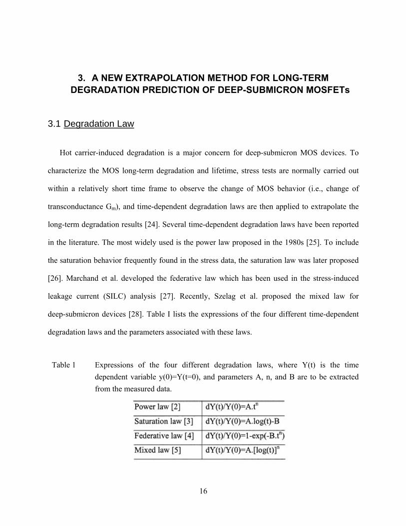
Hot carrier-induced degradation is a major concern for deep-submicron MOS devices. To
characterize the MOS long-term degradation and lifetime, stress tests are normally carried out
within a relatively short time frame to observe the change of MOS behavior (i.e., change of
transconductance Gm), and time-dependent degradation laws are then applied to extrapolate the
long-term degradation results [24]. Several time-dependent degradation laws have been reported
in the literature. The most widely used is the power law proposed in the 1980s [25]. To include
the saturation behavior frequently found in the stress data, the saturation law was later proposed
[26]. Marchand et al. developed the federative law which has been used in the stress-induced
leakage current (SILC) analysis [27]. Recently, Szelag et al. proposed the mixed law for
deep-submicron devices [28]. Table I lists the expressions of the four different time-dependent
degradation laws and the parameters associated with these laws.
Table 1 Expressions of the four different degradation laws, where Y(t) is the time dependent variable y(0)=Y(t=0), and parameters A, n, and B are to be extracted from the measured data.
17
3.2 New extrapolation method
Unfortunately, the long-term degradation phenomena observed experimentally do not obey
exactly any of the laws mentioned above, unless the parameters associated with the degradation
laws are extracted correctly from the short-term stress data measured. In this chapter, a new
extrapolation method will be developed and introduced to provide the degradation laws with a
better MOS lifetime predictability. Data measured from an NMOS and PMOS will be included
and analyzed in support of the model development. The method developed is simple yet highly
effective for the characterization of MOS reliability.
We propose a method called the exponential–exponential scale method to improve the
accuracy of the existing degradation laws. Conventionally, the stress data are placed on the
log–log scale, and least squares algorithm is used to fit the data and to extract the parameters
associated with the degradation law. Such an approach puts more weight on earlier data points
(data measured at earlier time frame). In reality, however, the long-term degradation is more
critical to the device lifetime, and thus the later data points should play a more important role on
the lifetime prediction. The exponential–exponential scale method proposed here puts the stress
data on the exponential–exponential scale. This in essence reverses the priority of the log–log
scale and places more emphasis on the later data points. As will be demonstrated later, this
method, when augmented into the existing degradation laws, improves significantly the accuracy
of the MOS lifetime prediction. To better illustrate the concept of the exponential–exponential
scale method proposed, let us consider an arbitrarily selected function 22.0220)( xxxf ×+×+= (3.1)
And its approximation
18
xBAxf ×+=′ )( (3.2)
Where A and B are parameters to be extracted. The original function f(x) in (3.1) is analogous to
the exact degradation (i.e., measured data) of MOSFET, while the approximated function f’(x) in
(3.2) is analogous to one of the power laws used to simulate the MOSFET long-term degradation.
Take a few data points of the original function at relatively small x (these data points are
analogous to those obtained from the short-term stress test of MOSFET), and these data points
can be arranged either
On the log–log or exponential–exponential scale. Using the least square fitting to these data,
different values for the parameters of A and B in (3.2) can be extracted. For example, using data
points from x = 0 to 10000, A and B were extracted to be A and B were extracted to be
-81.26733 and 101.03287 from the log-log scale method and -15999868.27 and 3601.99 from the
exponential–exponential scale method. Putting these values in (3.2), one can then predict the
trend of the original function at relatively large x based on the approximated function. Figure 9
compares the results of the original function, the approximated function with the log–log scale
method, and the approximated function with the exponential-exponential scale method for x up
to 40000. Clearly, the approximated function with the exponential-exponential scale method
compares more favorably with the original function than that with the log-log scale method.
3.3 MOS data analysis and degradation prediction
Let us first focus on the widely used power law, which in principle fits the data on the
log–log scale linearly. The devices considered were NMOS with a channel length of 0.18 μm and
channel width of 10 μm, stressed using the HP Network Analyzer (4156B) controlled by a PC
19
with Labview, under the bias condition of drain voltage VD = 2.2 v and gate voltage VG = 1.4 v.
Note that the substrate current reaches its peak value at this bias condition (i.e., worst stress
condition). Figure 10(a) shows the measured dGm/Gm(0) versus time characteristics on the
log–log scale for a relatively short stress time of 50000 s. The least squares fitting is also shown,
which is linear and appears to be accurate for the stress time considered. From the fitting, the
parameters A and n associated with the power law (see Table 1) were extracted to be 0.00000424
and 0.68908, respectively. These parameters, together with the power law, can then be used to
predict the long-term degradation.
Figure 9 Comparison of the original function f(x), the approximated function f’(x) with the log scale method, and the approximated function f’(x) with the exponential scale method. The approximated function were calculated based on the data points of the original function from x=0 to 10000
20
(a)
(b)
Figure 10 (a) Log-log scale and (b) exponential exponential scale (present method) fitting the of the measured dGm/Gm(0) characteristics up to 50000s.

21
As will be illustrated later, however, this approach gives rise to considerable errors in
predicting the Gm degradation at a relatively long stress time. On the other hand, instead of the
log–log scale, the exponential–exponential scale method (hereafter called the present method)
arranges the same measured stress data on the exponential–exponential scale, as shown in Figure
10(b). From this, together with the least squares algorithm, a new set of parameter values of A =
0.00077 and n = 0.39498 is extracted, and a more accurate long-term degradation prediction is
obtained.
It would be necessary to provide more explanations for the exponential-exponential scale
method shown in Figure 10(b). The tic marks on the x and y axis are based on exponential scales.
For example, the scale between 0 and 36889 tic marks on the x axis is exponential [i.e., opposite
to the log scale between the tic marks in Figure 10(a). The same applies to the y axis. Using the
same eight stress data points in Figure 10(a) but arranging them on this exponential–exponential
scale, together with the least squares fitting scheme, a more accurate set of parameters for the
power law can be extracted. These parameters are then put into the power law to predict
long-term degradation of MOS devices. Figure 11 compares the long-term dGm/Gm(0)
characteristics (up to about 250000 s) obtained from measurements, log–log scale method with
power law (i.e., power law), and present method with power law. In the fitting schemes, we used
the first 50000 s data [as shown in Figure 10(a) and (b) to predict the next 200000 s degradation
behavior. Clearly, the power law overestimates the Gm degradation at relatively long stress time.
Using a 10% Gm drop as the definition for the MOS lifetime, we obtained lifetimes of about
78000 and 210000 s from the power law and present method, respectively.
22
As mentioned earlier, the better accuracy associated with the present method stems from the
fact that such a method reverses the importance of the short-term stress data in the conventional
log–log scale method. In other words, the later data points obtained from the short-term stress
play a more important role in determining the parameters in the present method than that in the
log–log scale method. Since the MOS lifetime is a result of the long-term degradation, such a
reversal of importance in the present method gives rise to a more accurate prediction of the MOS
lifetime. The above discussions also brings an interesting question as to whether the accuracy of
the log–log scale method could be improved if one or more initial stress data points are not
considered, thus shifting the emphasis toward later data points. This is indeed the case, as the
error of the power law using the log–log scale method for predicting the MOS lifetime is reduced
from 62% to 12% if the first data point measured at 100 s [see Figure 10(a)] is removed from
consideration. Note that the error associated with the present method, without eliminating any
data point, is about 6%. The approach of removing initial data points, however, is quite
subjective and difficult to follow. This is because it is sometimes hard to know how many initial
data points need to be removed in order to achieve a reasonable accuracy, or if the first data point
is to be removed, at what stress time this data should be measured. If the first data point is
measured at a very small stress time, then the removal of this data may not improve the accuracy
of the log–log scale method. On the other hand, if the first data point is measured at a relatively
large stress time, the accuracy can be improved, but the subsequent data points will have to be
measured at even larger stress time, thus increasing the time needed for the initial stress
measurements. Moreover, a sufficiently large number of short-term stress data is often needed to
ensure consistent parameter extraction, and the removal of initial data may require additional

23
data to be measured at a larger stress time, which again prolongs the stress measurements. The
proposed exponential–exponential scale method eliminates these uncertainties and drawbacks.
An equally important issue to consider is how the selection of different numbers of
short-term data points, or the different short-term stress time, affects the accuracy of the
long-term degradation prediction. To address this, we have chosen four different short-term
stress times to predict the MOS long-term degradation using the power law with the log-log scale
method (i.e., power law) and with exponential-exponential scale method (i.e., present method).
Taking the measured lifetime of about 200000 s (see Figure 11) as the norm value, the lifetime
errors associated with the different short-term stress times were calculated and summarized in
Table 2. Obviously, the present method requires a much shorter stress time and thus much less
data points to obtain a reasonable accuracy in predicting the MOS long-term degradation than the
power law. For example, for the device under study, a stress time of 30000 s is sufficient for the
present model to predict the MOS lifetime with an error of less than 9%, whereas a nearly
ten-fold error is found in the power law based on the same stress data.
24
Figure 11 Comparison of dGm/Gm(0) characteristics of a 0.18-μm NMOS up to 250000 s
measured and predicted from the power law, saturation law, and the two laws with the present exponential-exponential method based on the short-term stress data (stress time of 50000s).
The present method can also be expanded to optimize other existing degradation laws. Also
shown in Figure 11 are the extrapolations of the saturation law (i.e., saturation law with the
log–log scale method) and the present method (i.e., saturation law with the
exponential–exponential scale method). It is illustrated that the saturation law can underestimate
considerably the long-term Gm degradation of deep-submicron MOS devices. Figure 12 shows
dGm/Gm(0) versus time characteristics obtained from measurements and from the fittings of the
federative law, mixed law, and the two laws with the exponential–exponential scale method. The
data here were taken from an SOI PMOS stressed under the bias conditions of VD= -4.25 V and
VG=VD/2 [29]. In the fitting schemes, the first 10000 s data were used to extrapolate the next
25
40000 s Gm degradation. The improved predictability of the present method is clearly
demonstrated. For this particular device, the mixed law appears to be more accurate than the
federative law.
Table 2 Errors of MOS lifetime associated with the power law and present method using
data measured for stress times up to 5000, 10000, 30000, and 50000s.
It should be mentioned that it is possible to fit the long-term Gm degradation reasonably well
using the existing degradation laws if the entire measured data points (i.e., up to 200000 s in
Figure 11 and up to 50000 s in Figure 12) are considered. On the other hand, when augmented
with the present method, these laws can predict the MOS long-term degradation accurately with
a relatively small number of short-term data points. In other words, using the present method, the
stress time required for predicting the MOS long-term degradation can be greatly reduced.
To further verify the present method, we analyzed the degradation of another NMOS with a
channel length of 0.18 μm stressed at VD=2.1 v and VG=1.33 v. Only the power law was
considered here, and a longer stress test was conducted to truly demonstrate the long-term
applicability of the model. Figure 13 shows Gm degradation results up to 420000 s obtained
from measurements and calculated from the power law with the log–log scale method (i.e.,
power law) and with the exponential-exponential scale method. The calculation results were
26
based on the short-term stress data measured up to 5000 s. The advantage of the
exponential–exponential scale method is again illustrated.
Figure 12 Comparison of dGm/Gm(0) characteristics of an SOI PMOS [6] up to 50000 s
measured and predicted from the fedrative law, and the two laws with the present exponential method based on the short-term stress data ( stress time of 10000 s).
27
Figure 13 Comparison of Gm degradation characteristics of 0.18-μm NMOS up to 400000 s measured and predicted from the power law and thhe power law with the present exponential method based on the short-term stress data (stress time of 5000 s)
3.4 Conclusion
In summary, a new and simple extrapolation method for the MOS lifetime prediction has
been developed. The method can be readily applied to any existing degradation law for better
accuracy and predictability. Stress data measured from three different MOS devices have been
analyzed, and the improved accuracy of the present method over the existing method has been
presented.
28
4. EMPIRICAL RELIABILITY MODELING FOR 0.18 μm MOS DEVICES
4.1 Introduction
Long-term hot-carrier induced degradation of MOS devices has become more severe as
the device size continues to scale down below 0.1 μm. As a consequence, the level of reliability
concern is increased when advanced MOSFETs are used in modern electronics systems. From
the designers’ perspective, it is imperative to have a simple and accurate reliability MOS model
which can predict the lifetime of MOSFET subject to different bias conditions.
Many physics-based MOS reliability models have been reported in the literature [30-31].
These models have the advantages of providing the physical insights into the degradation
mechanism in MOS devices, but they tend to have non-straightforward expressions and may not
be accurate due to the complicated short-channel and hot-carrier effects in the devices. Empirical
models developed based on experimental data, on the other hand, possess simple expressions and
provide accurate predictions, but they need to be re-developed for different MOS technologies.
This paper seeks to develop an accurate empirical reliability model for MOS devices
fabricated from the 0.18-μm technology. The model will be sufficiently versatile to account for
the effect of different channel lengths and different bias conditions. MOS devices having three
different channel lengths will be considered, and stress measurements on these devices under
different bias conditions will be conducted. The experimental data will then used as the basis of
parameter extraction and empirical model development.
29
4.2 Measurement procedure
The devices under study are n-channel MOSFETs fabricated from the 0.18-μm CMOS
technology, and the following channel lengths are considered: 0.5, 0.25, and 0.18 μm. The
channel width is 10 μm, and device make-ups include P-well, N-well, threshold-adjust implant,
and retrograde doping profiles. These devices are stressed over a relatively short period of time
at different bias conditions, and the degradation of transconductance Gm is measured in both the
linear and saturation regions. Based on these short-term stress data, the long-term degradation
and lifetime are then projected based on a time-dependent degradation law. The lifetime is
defined as the time when Gm degrades 10% from its initial value.
To predict the long-term Gm degradation and thus the MOS lifetime, we use the
well-known power law, which has the form of [32]
n
m
m CGG
τ×=Δ
(1) (4.1)
An extraction method is needed to determine the values of the two parameters (C and n)
associated with the power law. The conventional way to do this is to arrange the short-term stress
data on the log-log scale, as shown in Figure 14(a), and use the least-square fitting. Recently, we
have developed an improved extraction method which arranges the short-term data on the
exponential-exponential scale [34], as shown in Figure 14(b). In the figures, the short-term data
are measured up to 50000 sec. The different extraction methods will give rise to different
parameter values and thus to different long-term degradation results predicted by the power law.
Figure 15 compares the MOS long-term degradation characteristics (up to 200000 sec) obtained
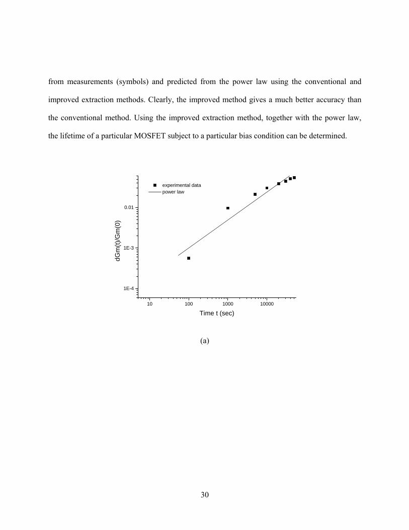
30
from measurements (symbols) and predicted from the power law using the conventional and
improved extraction methods. Clearly, the improved method gives a much better accuracy than
the conventional method. Using the improved extraction method, together with the power law,
the lifetime of a particular MOSFET subject to a particular bias condition can be determined.
10 100 1000 10000
1E-4
1E-3
0.01
experimental data power law
dGm
(t)/G
m(0
)
Time t (sec)
(a)
31
(b)
Figure 14 Short-term (up to 50000 sec) stress transconductance data measured and fitted based on (a) log-log scale and (b) exponential-exponential scale.
0 50000 100000 150000 200000-0.02
0.00
0.02
0.04
0.06
0.08
0.10
0.12
0.14
0.16
0.18
0.20 experimental data power law with log-log method power law with improved method
dGm
(t)/G
m(0
)
Time t (sec)
Figure 15 Long-term (up to 200000 sec) transconductance degradation obtained from measurements, power law with log-log method, and power law with exponential-exponential method.
32
4.3 Empirical model development
Our task here is to develop an empirical reliability model for the 0.18-μm NMOS devices
having different channel lengths L and different drain voltages VD under the worst-case stress
condition. This means that, for a MOS device having a particular L and VD, the stress is done in
such a condition that the gate voltage VG is adjusted until the substrate current IB is maximum.
As such, VG is a hidden variable and does not appear in the empirical model.
Let us first focus on the MOS degradation in the linear region (MOS devices stressed
under the worst-case and measured at a drain voltage of 0.1 v). To develop the empirical model,
we will first look into the relationship between MOS lifetime τ and substrate current IB. It has
been observed experimentally that τ versus IB characteristics are not a function of L. This is
because IB is related to the maximum electric field Em near the drain junction, which gives a
direct measure of the stress level [34]. Once IB is fixed, Em is almost insensitive to the channel
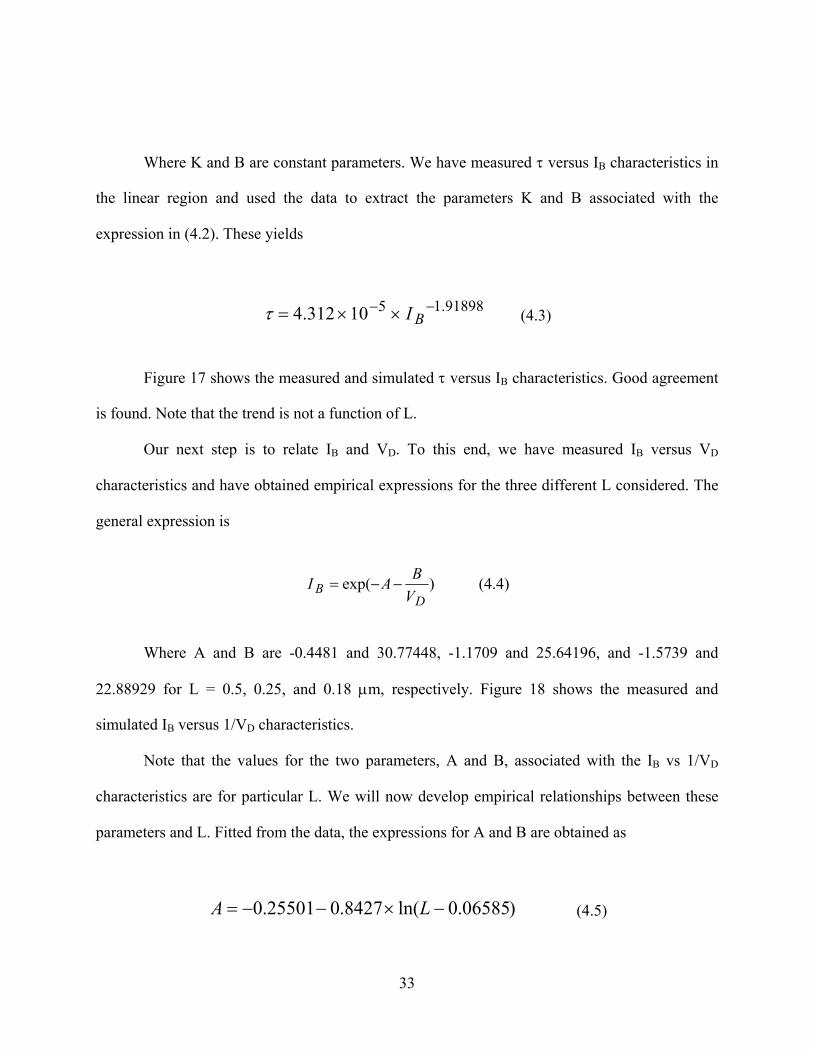
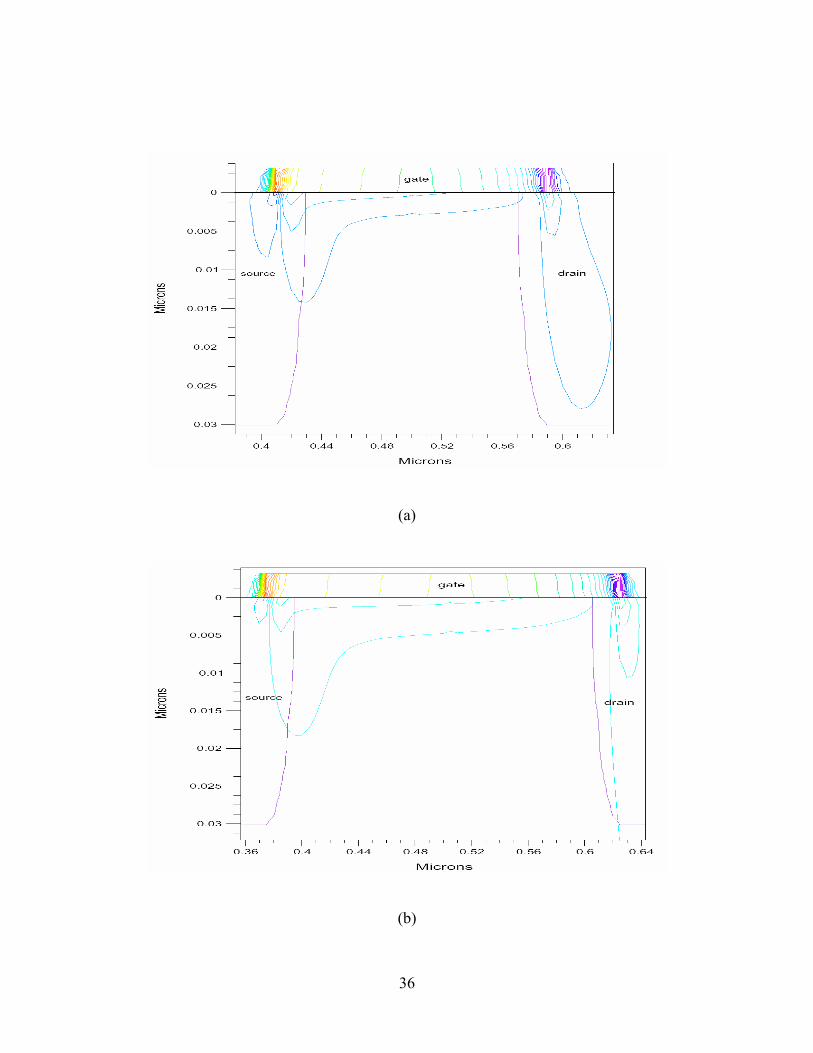
length L. To illustrate this, we have carried out device simulation and shown the electric field
contours in MOS devices having the same IB of 4.4x10⁻⁶ A, but three different channel lengths of
0.5, 0.25, and 0.18 μm in Figure 16(a)-(c), respectively. Note that different drain voltages are
needed to arrive at the same substrate current for the MOS devices with three different L. Very
similar maximum fields of 6.1x10⁵, 6.3x10⁵, and 6.4x10⁵V/cm are found in these devices. This
clearly indicates that Em is almost independent of L when IB is constant. In other words, once IB
is fixed, the stress level, and thus the MOS degradation, is almost the same for MOS devices
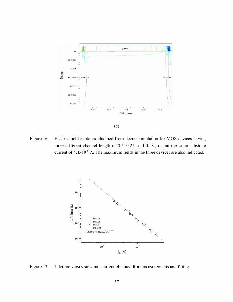
having different L. An expression has been suggested to relate the lifetime τ and IB [30]:
BBIK −×=τ (4.2)
33
Where K and B are constant parameters. We have measured τ versus IB characteristics in
the linear region and used the data to extract the parameters K and B associated with the
expression in (4.2). These yields
91898.1510312.4 −− ××= BIτ (4.3)
Figure 17 shows the measured and simulated τ versus IB characteristics. Good agreement
is found. Note that the trend is not a function of L.
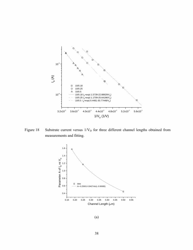
Our next step is to relate IB and VD. To this end, we have measured IB versus VD
characteristics and have obtained empirical expressions for the three different L considered. The
general expression is
)exp(D
B VBAI −−= (4.4)
Where A and B are -0.4481 and 30.77448, -1.1709 and 25.64196, and -1.5739 and
22.88929 for L = 0.5, 0.25, and 0.18 μm, respectively. Figure 18 shows the measured and
simulated IB versus 1/VD characteristics.
Note that the values for the two parameters, A and B, associated with the IB vs 1/VD
characteristics are for particular L. We will now develop empirical relationships between these
parameters and L. Fitted from the data, the expressions for A and B are obtained as
)06585.0ln(8427.025501.0 −×−−= LA (4.5)
34
19081.0)09393.0(54878.36 −×= LB (4.6)
Figure 19 (a) and (b) compare the measured and fitting data of A and B, respectively.
We can now combine the above expressions and obtain an empirical model for MOS
lifetime as a function of VD and L. Specifically, we put (4.5) and (4.6) into (4.4), and then put the
resulting equation into (4.3). This leads to the following expression for τ as a function of VD and
L:
91898.1190813.0
5 ]})09393.0(54878.36)06585.0ln(8421.025501.0{exp[1031205.4 −− −×−−×+××=
DVLLτ
(4.7)
The above equation is for MOS devices operated in the linear region. Using the same
approach, we can also develop an empirical model for MOS devices in the saturation region
(MOS devices stressed under the worst-case and measured at a drain voltage of 0.9 V):
94396.0190813.0
]})09393.0(54878.36)06585.0ln(8421.025501.0{exp[36215.22 −−×−−×+×=
DVLLτ
(4.8)
Figure 20 and 21 show the measured and simulated τ versus 1/VD as a function of L for
MOSFETs operated in the linear and saturation regions, respectively. Note that while the
majority of lifetimes (open symbols) were obtained from the projection of the power law based
35
on short-term stress data, a few lifetimes (closed symbols) were actually long-term stress data
measured all the way to the 10% Gm degradation. Very good agreement between the model and
measurements is obtained.
The model developed is highly useful to provide MOS design guide concerning reliability
issues. For example, for a given MOS device and a specific lifetime time, one can determine the
maximum VD allowed to apply to the device, or one can determine the minimum channel length
for a known VD and lifetime. Tables 3 and 4 give the specifics of such information.
Table 3 Maximum drain voltage (in V) allowed for the specific lifetime and channel
length VD Lifetime\Length 0.18μm 0.25μm 0.35μm 0.5μm
3 Yrs 1.729 1.880 2.013 2.143
5 Yrs 1.695 1.844 1.975 2.104
Linear
Region
10 Yrs 1.651 1.797 1.926 2.053
3Yrs 1.569 1.710 1.835 1.958
5 Yrs 1.513 1.651 1.772 1.893
Saturation
Region
10 Yrs 1.443 1.576 1.694 1.811
Table 4 Minimum channel length (in μm) allowed for the specific lifetime and drain
voltage
Channel length Lifetime\VD 0.9V 1.2V 1.5V 1.8V
3 Yrs 0.096 0.102 0.127 0.208
5 Yrs 0.096 0.104 0.132 0.225
Linear
Region
10 Yrs 0.096 0.105 0.139 0.252
3 Yrs 0.097 0.110 0.158 0.318
5 Yrs 0.098 0.114 0.175 0.379
Saturation
Region
10 Yrs 0.099 0.121 0.206 0.483
36
(a)
(b)
37
(c)
Figure 16 Electric field contours obtained from device simulation for MOS devices having three different channel length of 0.5, 0.25, and 0.18 μm but the same substrate current of 4.4x10⁻⁶ A. The maximum fields in the three devices are also indicated.
10-6 10-5
104
105
106
107
10/0.18 10/0.25 10/0.5 linear fit
Lifetime=4.312x10⁻⁵xIB-1.91898
Life
time
(s)
IB (A)
Figure 17 Lifetime versus substrate current obtained from measurements and fitting.
38
3.2x10⁻¹ 3.6x10⁻¹ 4.0x10⁻¹ 4.4x10⁻¹ 4.8x10⁻¹ 5.2x10⁻¹ 5.6x10⁻¹
10-6
10-5
10/0.18 10/0.25 10/0.5 10/0.18 IB=exp(-1.5739-22.88929/VD) 10/0.25 IB=exp(-1.1709-25.64196/VD) 10/0.5 IB=exp(-0.4481-30.77448/VD)
I B (A
)
1/VD (1/V)
Figure 18 Substrate current versus 1/VD for three different channel lengths obtained from measurements and fitting.
0.15 0.20 0.25 0.30 0.35 0.40 0.45 0.50 0.55
0.4
0.6
0.8
1.0
1.2
1.4
1.6
data A=-0.25501-0.8427xln(L-0.06585)P
aram
eter
A o
f IB
vs V
D
Channel Length (μm)
(a)
39
0.15 0.20 0.25 0.30 0.35 0.40 0.45 0.50 0.5522
24
26
28
30
32
data
B=36.54878*(L-0.09393)0.19081
Par
amet
er B
of I
B vs
V D
Channel Length (μm)
(b)
Figure 19 Measured and fitting data of (a) parameter A and (b) parameter B.
0.32 0.36 0.40 0.44 0.48 0.52 0.56 0.60103
104
105
106
107
108
109
1010
1011
10/0.18 10/0.25 10/0.5 10/0.18 true experimental data 10/0.25 true experimental data 10/0.5 true experimental data 10/0.18 10/0.25 10/0.35 10/0.5
Life
time
(s)
1/VD (1/v)
Figure 20 Lifetime versus 1/VD in the linear region obtained from measurements and empirical model. Open symbols are lifetimes obtained from power law projection based on short-term stress data, and close symbols are lifetimes obtained from the long-term stress measured all the way to the 10% transconductance degradation.
40
0.32 0.36 0.40 0.44 0.48 0.52 0.56 0.60
105
106
107
108
109
10/0.18 experimental data 10/0.25 experimental data 10/0.5 experimental data 10/0.18 simulation 10/0.25 simulation 10/0.35 simulation 10/0.5 simulation
Life
time
(s)
1/VD (1/V)
Figure 21 Lifetime versus 1/VD in the saturation region obtained from measurements and empirical model.
4.4 Conclusion
Reliability is a major concern for modern deep-submicron MOS devices. In this study,
n-channel MOSFETs fabricated from the 0.18-μm CMOS technology and subjected to different
bias conditions were considered. Short-term stress data were first measured, and the MOS’s
long-term transconductance degradation and lifetimes were projected from the power law. Fitting
to these data, an empirical model for predicting the MOS lifetime as a function of the channel
length and drain voltage has been developed. This study provides useful design guides
concerning MOS reliability issues, and the approach developed can be readily extended to the
empirical modeling of other semiconductor devices.
41
5. SUBSTRATE CURRENT, GATE CURRENT, GATE CURRENT AND LIFETIME PREDICTION OF DEEP-SUBMICRON nMOS DEVICES
5.1 Introduction
Being scaled down to the deep-submicron range, the MOS transistors have suffered from
various large leakage currents and significant reliability degradation [35-37]. The long-term
reliability of MOS devices is governed by the hot carrier irradiation effects, which are often
characterized with the substrate current or gate current [38-40]. The device reliability parameters,
e.g. threshold voltage shift and transconductance degradations, are often found to be power
functions of the stressing duration. The power time dependence is extrapolated to estimate the
device lifetime [38-39]. However, there are many reports suggesting that the device degradation
does not follow the power law and the lifetime prediction based on the extrapolation of the
power law can be questionable [40-43].
Besides the lifetime model, the MOS degradation characterization has become more difficult
because of the presence of large gate leakage currents. In deep-submicron devices, the thickness
of silicon gate oxide has been scaled down to the direct-tunneling limit (<3 nm) [37]; as a result,
the measured gate current may not represent the actual amount of the hot-carrier current involved
in the device degradation. In addition, this tunneling process has pronounced effects on the
mechanism of charge trapping in the oxide which is a main origin of the threshold voltage shift
in short-channel devices. Hence, the relationships amongst the threshold voltage shift, the gate
current, and the substrate current are more complicated and less straightforward. This work aims
at the investigation of physical mechanisms underlying the hot-carrier stressing induced
42
characteristic degradation in deep-submicron devices based on the observation of the gate and
substrate currents. With a better understanding of substrate and gate currents, a more precise
MOS device lifetime fitting model will be developed. Experimental details will be given in Sec.
5.2 Sec 5.3.1 demonstrates the inaccuracy of the MOS lifetime prediction based on the existing
methods, and a new prediction method will be proposed in Sec. 5.3.2. Further comments on the
power-law model and the newly proposed model will be given in Sec. 5.4. Finally, major results
of this work will be summarized in Sec. 5.5.
5.2 Experiments
N-channel deep-submicron MOS devices fabricated using the 0.18-μm CMOS technology
are considered. The channel width of the devices is 10 μm and the gate oxide thickness is 3.2 nm.
Three different channel lengths of 0.18, 0.25, and 0.5 μm were used to study the effect of
channel length on the device degradation characteristics. Substrate current stressing and device
characteristic measurements were carried out with an HP 4156 Precision Semiconductor
Parameter Analyzer. In the experiments, the devices were biased at the worst-case stress
condition, i.e., at maximum substrate current (ISub). The gate currents (IG) were also measured
under the same stress condition. Unless noted otherwise, MOS lifetimes were determined using
the criteria of 10% shift in the threshold voltage (VT), which was measured based on
extrapolating the point where the slope of drain current vs. gate voltage curve is maximum.
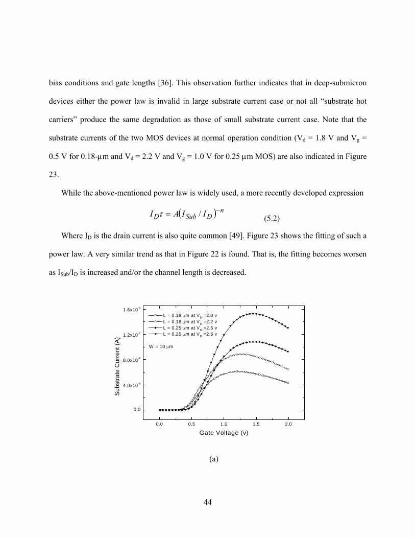
Figure 22(a) shows ISub vs. gate voltage Vg characteristics as a function of the drain voltage Vd
for the MOS devices considered, and Figure 22(b) shows the drain current ID , substrate current
ISub and gate current IG vs. Vd characteristics under the worst-case stress condition (i.e., Vg is
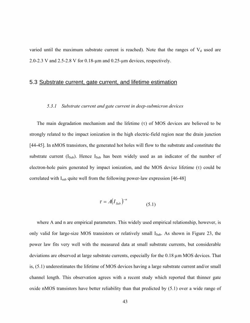
43
varied until the maximum substrate current is reached). Note that the ranges of Vd used are
2.0-2.3 V and 2.5-2.8 V for 0.18-µm and 0.25-µm devices, respectively.
5.3 Substrate current, gate current, and lifetime estimation
5.3.1 Substrate current and gate current in deep-submicron devices
The main degradation mechanism and the lifetime (τ) of MOS devices are believed to be
strongly related to the impact ionization in the high electric-field region near the drain junction
[44-45]. In nMOS transistors, the generated hot holes will flow to the substrate and constitute the
substrate current (ISub). Hence ISub has been widely used as an indicator of the number of
electron-hole pairs generated by impact ionization, and the MOS device lifetime (τ) could be
correlated with Isub quite well from the following power-law expression [46-48]
( ) nSubIA −=τ (5.1)
where A and n are empirical parameters. This widely used empirical relationship, however, is
only valid for large-size MOS transistors or relatively small ISub. As shown in Figure 23, the
power law fits very well with the measured data at small substrate currents, but considerable
deviations are observed at large substrate currents, especially for the 0.18 μm MOS devices. That
is, (5.1) underestimates the lifetime of MOS devices having a large substrate current and/or small
channel length. This observation agrees with a recent study which reported that thinner gate
oxide nMOS transistors have better reliability than that predicted by (5.1) over a wide range of
44
bias conditions and gate lengths [36]. This observation further indicates that in deep-submicron
devices either the power law is invalid in large substrate current case or not all “substrate hot
carriers” produce the same degradation as those of small substrate current case. Note that the
substrate currents of the two MOS devices at normal operation condition (Vd = 1.8 V and Vg =
0.5 V for 0.18-μm and Vd = 2.2 V and Vg = 1.0 V for 0.25 μm MOS) are also indicated in Figure
23.
While the above-mentioned power law is widely used, a more recently developed expression
( ) nDSubD IIAI −= /τ (5.2)
Where ID is the drain current is also quite common [49]. Figure 23 shows the fitting of such a
power law. A very similar trend as that in Figure 22 is found. That is, the fitting becomes worsen
as ISub/ID is increased and/or the channel length is decreased.
0.0 0.5 1.0 1.5 2.0
0.0
4.0x10⁻⁶
8.0x10⁻⁶
1.2x10⁻⁵
1.6x10⁻⁵
L = 0.18 μm at VD =2.0 v L = 0.18 μm at VD =2.2 v L = 0.25 μm at VD =2.5 v L = 0.25 μm at VD =2.6 v
W = 10 μm
Subs
trate
Cur
rent
(A)
Gate Voltage (v)
(a)
45
2.0 2.1 2.2 2.3 2.4 2.5 2.6 2.7 2.8
10-10
10-8
10-6
10-4
10-2
W orst-case stress condition
ID @ L = 0.18 μm W = 10 μm ID @ L = 0.25 μm W = 10 μm Isub @ L = 0.18 μm W = 10 μm Isub @ L = 0.25 μm W = 10 μm IG @ L = 0.18 μm W = 10 μm IG @ L = 0.25 μm W = 10 μm
Dra
in C
urre
nt, S
ubst
rate
Cur
rent
, Gat
e cu
rrent
(A)
Drain Voltage (v)
(b) Figure 22 (a) Substrate current vs. gate voltage characteristics (b) drain current, substrate
current and gate current vs. drain voltage characteristics under the worst-case stress condition (i.e., maximum substrate current)
Substrate Current (A)
10-6 10-5 10-4
Life
time
(s)
104
105
106
107
108
109L = 0.18 μm mesuredL = 0.18 μm fittingL = 0.25 μm mesuredL = 0.25 μm fitting
Threshold Voltage Lifetime
ISUB (normal) L = 0.18 μm
ISUB (normal) L = 0.25 μm
Figure 23 Power-law fitting of 0.18 μm and 0.25 μm MOS devices. Markers are the experimental data and lines are the curve fittings using the power law of ID=A(ISub/ID)-n.
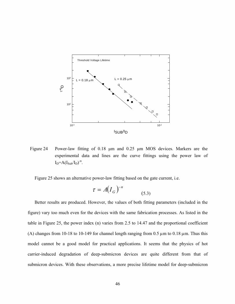
46
ISUB/ID
10-3 10-2
τ *I D
102
103
Threshold Voltage Lifetime
L = 0.18 μm L = 0.25 μm
Figure 24 Power-law fitting of 0.18 μm and 0.25 μm MOS devices. Markers are the
experimental data and lines are the curve fittings using the power law of ID=A(ISub/ID)-n.
Figure 25 shows an alternative power-law fitting based on the gate current, i.e.
( ) nGIA −=τ (5.3)
Better results are produced. However, the values of both fitting parameters (included in the
figure) vary too much even for the devices with the same fabrication processes. As listed in the
table in Figure 25, the power index (n) varies from 2.5 to 14.47 and the proportional coefficient
(A) changes from 10-18 to 10-149 for channel length ranging from 0.5 μm to 0.18 μm. Thus this
model cannot be a good model for practical applications. It seems that the physics of hot
carrier-induced degradation of deep-submicron devices are quite different from that of
submicron devices. With these observations, a more precise lifetime model for deep-submicron
47
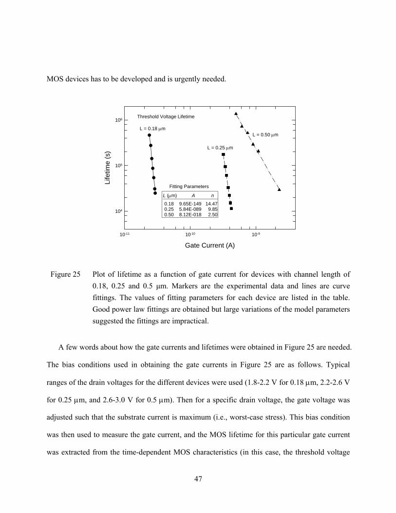
MOS devices has to be developed and is urgently needed.
Gate Current (A)
10-11 10-10 10-9
Life
time
(s)
104
105
106 Threshold Voltage Lifetime
L = 0.18 μm
L = 0.25 μm
L = 0.50 μm
L (μm) A n
0.18 9.65E-149 14.470.25 5.84E-089 9.850.50 8.12E-018 2.50
Fitting Parameters
Figure 25 Plot of lifetime as a function of gate current for devices with channel length of 0.18, 0.25 and 0.5 μm. Markers are the experimental data and lines are curve fittings. The values of fitting parameters for each device are listed in the table. Good power law fittings are obtained but large variations of the model parameters suggested the fittings are impractical.
A few words about how the gate currents and lifetimes were obtained in Figure 25 are needed.
The bias conditions used in obtaining the gate currents in Figure 25 are as follows. Typical
ranges of the drain voltages for the different devices were used (1.8-2.2 V for 0.18 μm, 2.2-2.6 V
for 0.25 μm, and 2.6-3.0 V for 0.5 μm). Then for a specific drain voltage, the gate voltage was
adjusted such that the substrate current is maximum (i.e., worst-case stress). This bias condition
was then used to measure the gate current, and the MOS lifetime for this particular gate current
was extracted from the time-dependent MOS characteristics (in this case, the threshold voltage
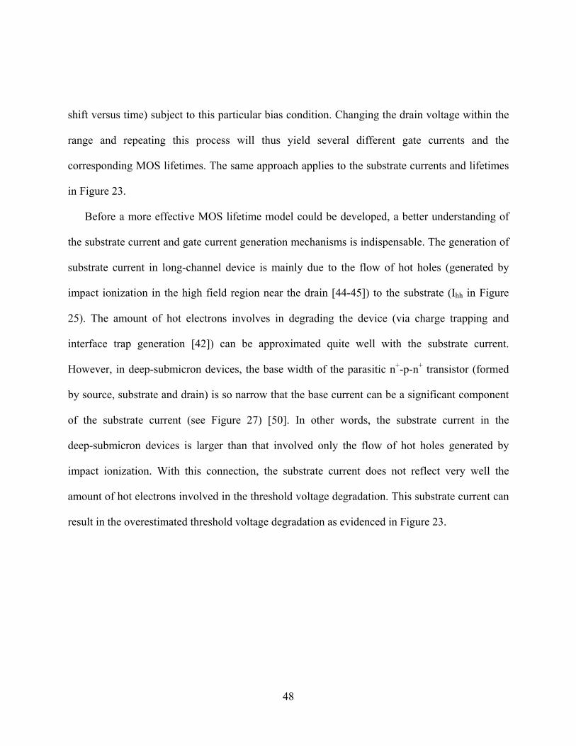
48
shift versus time) subject to this particular bias condition. Changing the drain voltage within the
range and repeating this process will thus yield several different gate currents and the
corresponding MOS lifetimes. The same approach applies to the substrate currents and lifetimes
in Figure 23.
Before a more effective MOS lifetime model could be developed, a better understanding of
the substrate current and gate current generation mechanisms is indispensable. The generation of
substrate current in long-channel device is mainly due to the flow of hot holes (generated by
impact ionization in the high field region near the drain [44-45]) to the substrate (Ihh in Figure
25). The amount of hot electrons involves in degrading the device (via charge trapping and
interface trap generation [42]) can be approximated quite well with the substrate current.
However, in deep-submicron devices, the base width of the parasitic n+-p-n+ transistor (formed
by source, substrate and drain) is so narrow that the base current can be a significant component
of the substrate current (see Figure 27) [50]. In other words, the substrate current in the
deep-submicron devices is larger than that involved only the flow of hot holes generated by
impact ionization. With this connection, the substrate current does not reflect very well the
amount of hot electrons involved in the threshold voltage degradation. This substrate current can
result in the overestimated threshold voltage degradation as evidenced in Figure 23.
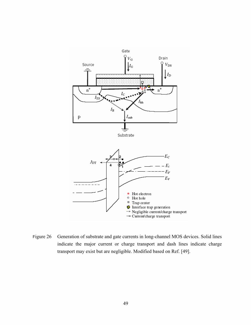
49
Figure 26 Generation of substrate and gate currents in long-channel MOS devices. Solid lines indicate the major current or charge transport and dash lines indicate charge transport may exist but are negligible. Modified based on Ref. [49].
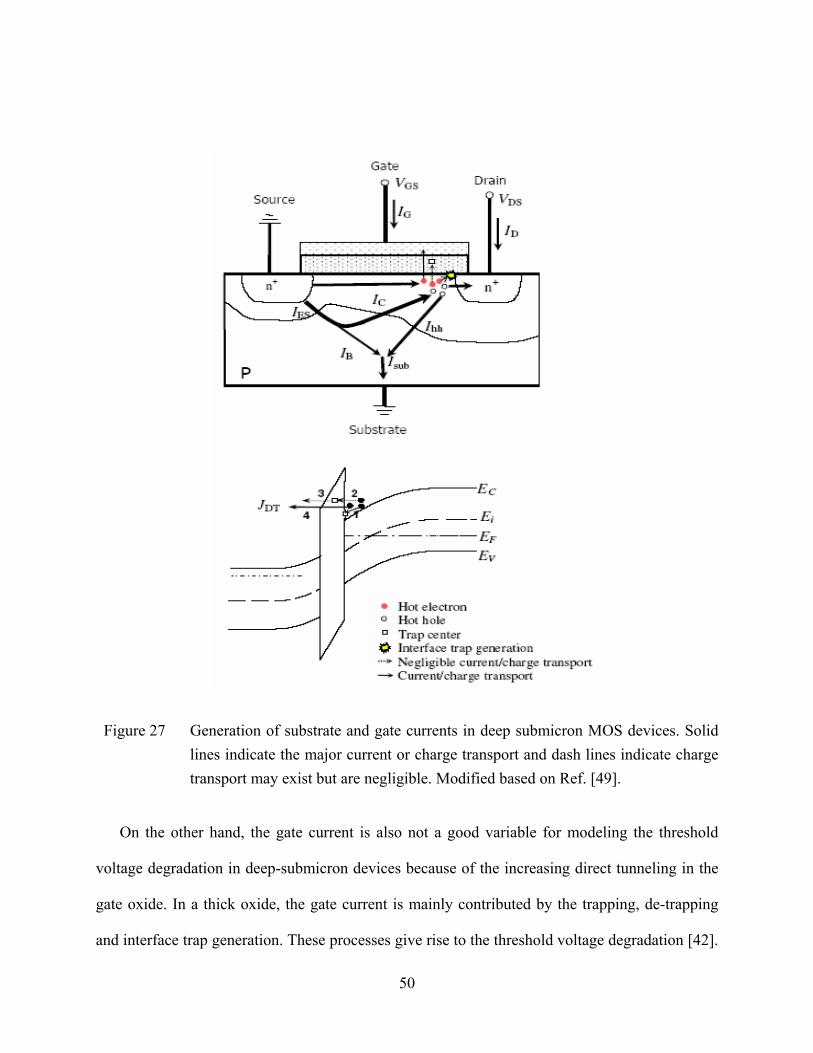
50
Figure 27 Generation of substrate and gate currents in deep submicron MOS devices. Solid lines indicate the major current or charge transport and dash lines indicate charge transport may exist but are negligible. Modified based on Ref. [49].
On the other hand, the gate current is also not a good variable for modeling the threshold
voltage degradation in deep-submicron devices because of the increasing direct tunneling in the
gate oxide. In a thick oxide, the gate current is mainly contributed by the trapping, de-trapping
and interface trap generation. These processes give rise to the threshold voltage degradation [42].

51
However, in a very thin gate oxide, a large part of the gate current comes from the direct
tunneling of hot electrons in the impact ionization region or electrons in the channel, and the
oxide trapping and de-trapping effect will also become less significant because the oxide is so
thin that the rate of tunneling from the trap is high (see Figure 27). This tunneling current does
not cause electron trapping in the gate oxide and thus does not produce threshold voltage shift.
When the gate current is increased (i.e., stress is increased), a portion of the gate current
produces trapped oxide charges, whereas the other portion of the gate current actually reduces
such charges. As a result, a smaller number of trapping charges takes place in the thinner gate
oxide [41]. Hence, the lifetime of deep-submicron MOS devices can be underestimated if the
characterization is based either on the substrate current or the gate current.
5.3.2 New lifetime estimation model
As shown in Figure 27, the substrate current and gate current in deep-submicron device
consist of “non-degrading” current components. Hence, neither the substrate nor gate current is a
good measure of the amount of hot electrons involved in the threshold voltage degradation. A
precise way to quantify this degradation will be too difficult, as the non-degrading currents
cannot be separated from the total current using any known experimental methods. Since the
measured substrate and gate currents are the only readily accessible data for characterization
purposes, any approach based on these currents but can suppress the “non-degrading” (does not
lead to device degradation) part and make the degrading part more relevant would be highly
attractive and lead to a better estimation of the MOS device lifetime.
Since the non-degrading gate current is strongly related to the non-degrading substrate
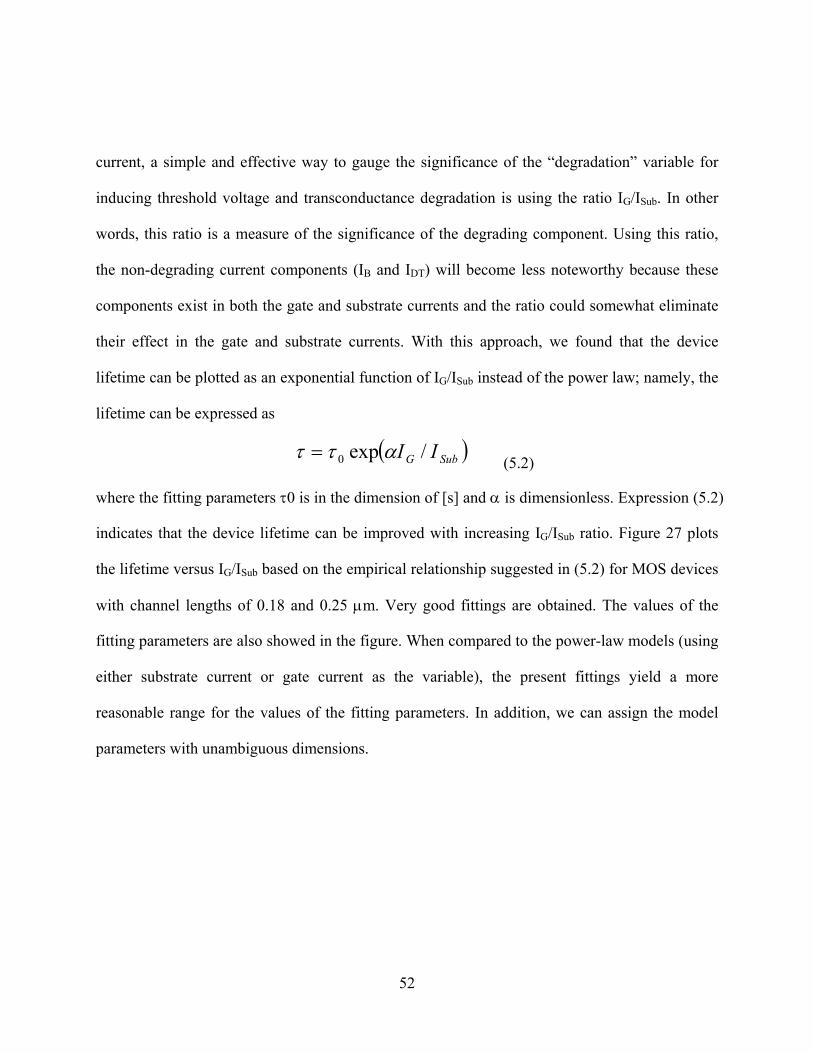
52
current, a simple and effective way to gauge the significance of the “degradation” variable for
inducing threshold voltage and transconductance degradation is using the ratio IG/ISub. In other
words, this ratio is a measure of the significance of the degrading component. Using this ratio,
the non-degrading current components (IB and IDT) will become less noteworthy because these
components exist in both the gate and substrate currents and the ratio could somewhat eliminate
their effect in the gate and substrate currents. With this approach, we found that the device
lifetime can be plotted as an exponential function of IG/ISub instead of the power law; namely, the
lifetime can be expressed as
( )SubG II /exp0 αττ = (5.2)
where the fitting parameters τ0 is in the dimension of [s] and α is dimensionless. Expression (5.2)
indicates that the device lifetime can be improved with increasing IG/ISub ratio. Figure 27 plots
the lifetime versus IG/ISub based on the empirical relationship suggested in (5.2) for MOS devices
with channel lengths of 0.18 and 0.25 μm. Very good fittings are obtained. The values of the
fitting parameters are also showed in the figure. When compared to the power-law models (using
either substrate current or gate current as the variable), the present fittings yield a more
reasonable range for the values of the fitting parameters. In addition, we can assign the model
parameters with unambiguous dimensions.
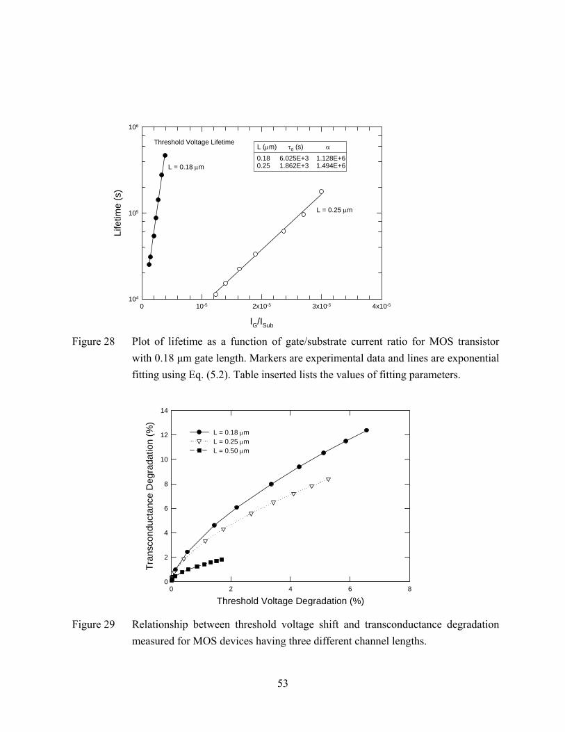
53
IG/ISub
0 10-5 2x10⁻⁵ 3x10⁻⁵ 4x10⁻⁵
Life
time
(s)
104
105
106
Threshold Voltage Lifetime
0.18 6.025E+3 1.128E+60.25 1.862E+3 1.494E+6
L (μm) τ0 (s) α
L = 0.18 μm
L = 0.25 μm
Figure 28 Plot of lifetime as a function of gate/substrate current ratio for MOS transistor
with 0.18 μm gate length. Markers are experimental data and lines are exponential fitting using Eq. (5.2). Table inserted lists the values of fitting parameters.
Threshold Voltage Degradation (%)0 2 4 6 8
Tran
scon
duct
ance
Deg
rada
tion
(%)
0
2
4
6
8
10
12
14
L = 0.18 μm L = 0.25 μmL = 0.50 μm
Figure 29 Relationship between threshold voltage shift and transconductance degradation
measured for MOS devices having three different channel lengths.
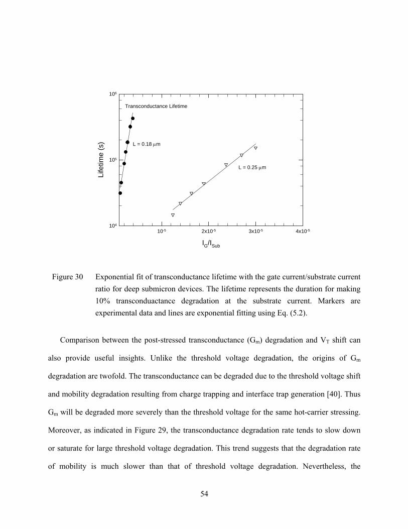
54
IG/ISub
10-5 2x10⁻⁵ 3x10⁻⁵ 4x10⁻⁵
Life
time
(s)
104
105
106
Transconductance Lifetime
L = 0.18 μm
L = 0.25 μm
Figure 30 Exponential fit of transconductance lifetime with the gate current/substrate current ratio for deep submicron devices. The lifetime represents the duration for making 10% transconduactance degradation at the substrate current. Markers are experimental data and lines are exponential fitting using Eq. (5.2).
Comparison between the post-stressed transconductance (Gm) degradation and VT shift can
also provide useful insights. Unlike the threshold voltage degradation, the origins of Gm
degradation are twofold. The transconductance can be degraded due to the threshold voltage shift
and mobility degradation resulting from charge trapping and interface trap generation [40]. Thus
Gm will be degraded more severely than the threshold voltage for the same hot-carrier stressing.
Moreover, as indicated in Figure 29, the transconductance degradation rate tends to slow down
or saturate for large threshold voltage degradation. This trend suggests that the degradation rate
of mobility is much slower than that of threshold voltage degradation. Nevertheless, the
55
transconductance degradation can still be fitted very well with the exponential function in (5.2)
using IG/ISub as the degradation variable, as shown in Figure 30. In this figure, the MOS lifetime
is defined as the time when Gm degrades 10% from its initial value. This result again
demonstrates that IG/ISub is a good measure of the physical mechanisms underlying the
deep-submicron MOS transistor degradation.
5.4 Discussions
Although the power-law degradation models are often used in fitting the experimental data of
hot-carrier induced degradation, non-power law relationships have also been reported [40-43]. A
disadvantage of the power law fitting is that its fitting parameters have arbitrary dimensions (and
thus it is impossible to establish the physics and relationship with the device parameters) [42]. In
the present model, the model parameters have unambiguous dimensions. In addition, the range of
the parameters’ values is more reasonable and well behaved than that of the power-law models
(see Figure 27).
Meanwhile, the extrapolation of the conventional power-law methods is also questionable. It
implies that the VT shift can be increased without limit as the stressing goes on. The degradable
quantities, e.g. Si-Si bonds or hydrogen bonds, will finally consume up and the degradation will
reach a maximum value [42, 51-53]. It has long been suspected that the power-law fitting cannot
represent well the stress-induced degradation of the MOS devices for all cases [42]. Depending
on different trapping and generation rates, the degradation behavior in fact can be modeled in
exponential law, power law, or exponential law with a quasi-saturation region [42]. An
exponential law with the ratio IG/ISub has been proposed in this work and it is encouraging that
56
such an empirical model fits very well both the threshold voltage and transconductance
degradation behavior in advanced MOS devices.
In summary, although the present model is still an empirical one, the correct device physics is
indeed imbedded in the ratio IG/ISub, thereby making the proposed method more effective. In
addition, the fitting parameters are well behaved and vary within a reasonable range. Note that
expression (5.2) is also valid in extreme cases. When there is no substrate current (no hot carriers
generated), the lifetime will be infinite. When the substrate current is extremely large, the lower
bound of the lifetime is τ0, which indicates that the device degradation reaches a maximum value.
When the gate current approaches zero, severe degradation occurs because most of charges are
trapped in the oxide and produces large threshold voltage shift and transconductance degradation.
The lifetime is improved when the gate current is large (e.g. with direct tunneling in the oxide)
because the amount of charge trapping in the oxide is reduced. Of course, further experimental
validation and investigation on the relationship between model parameters and devices will help
to make the present model with stronger physical justification.
5.5 Conclusion
In summary, we have shown clearly that the conventional power-law empirical models
for MOS lifetime versus substrate/gate current characteristics are valid only for the cases of
relatively long channel devices and/or relatively small stress conditions. These models
underestimate the lifetime for deep-submicron MOS devices. This effect can be attributed to the
“non-degrading” components of the substrate and gate currents. A simple and accurate empirical
expression correlating the MOS lifetime with the ratio of gate to substrate current has been
57
proposed, and it can serve as an effective alternative to the power-law models for the lifetime
prediction of modern and future MOS devices.
58
6. A SPICE-LIKE RELIABILITY MODEL FOR DEEP-SUBMICRON CMOS TECHNOLOGY
6.1 Introduction
Due to continue down scaling, the channel electric field increases and the hot-carrier (HC)
effect becomes more significant [54]. When the oxide thickness is scaled down to 3 nm,
deep-submicron nMOS transistors have different reliability mechanism compare with the
long-channel devices [55-56]. As a result, the conventional modeling for hot-carrier aging is
questionable for deep-submicron devices, and a systematic method is needed for predicting the
lifetime of the devices and circuits.
In this paper, we develop a Spice-like reliability model for advanced radio frequency RF
MOS devices and implement the model into SpectreRF circuit simulator via Verilog-A HDL
(Hardware Description Language).
6.2 Methodology
While many studies have been devoted to the field of MOSFET reliability, most of the works
were focused on the device-level modeling [57-60] and not much attention has been paid to
develop a model which is suitable for reliability simulation of MOS circuits. There is no new
systemic and transplantable methodology to study MOS circuit performance degradations due to
the hot-carrier effects. A widely used reliability simulation tool called the BERT (Berkeley
Reliability Tool) was introduced in 1993.
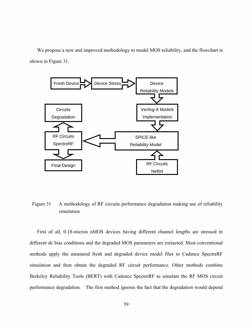
59
We propose a new and improved methodology to model MOS reliability, and the flowchart is
shown in Figure 31.
Figure 31 A methodology of RF circuits performance degradation making use of reliability
simulation
First of all, 0.18-micron nMOS devices having different channel lengths are stressed in
different dc bias conditions and the degraded MOS parameters are extracted. Most conventional
methods apply the measured fresh and degraded device model files to Cadence SpectreRF
simulation and then obtain the degraded RF circuit performance. Other methods combine
Berkeley Reliability Tools (BERT) with Cadence SpectreRF to simulate the RF MOS circuit
performance degradation. The first method ignores the fact that the degradation would depend
Fresh Device Device Stress Device
Reliability Models
Verilog-A Models
Implementation
SPICE-like
Reliability Model
RF Circuits
SpectreRF
Final Design
Circuits
Degradation
RF Circuits
Netlist
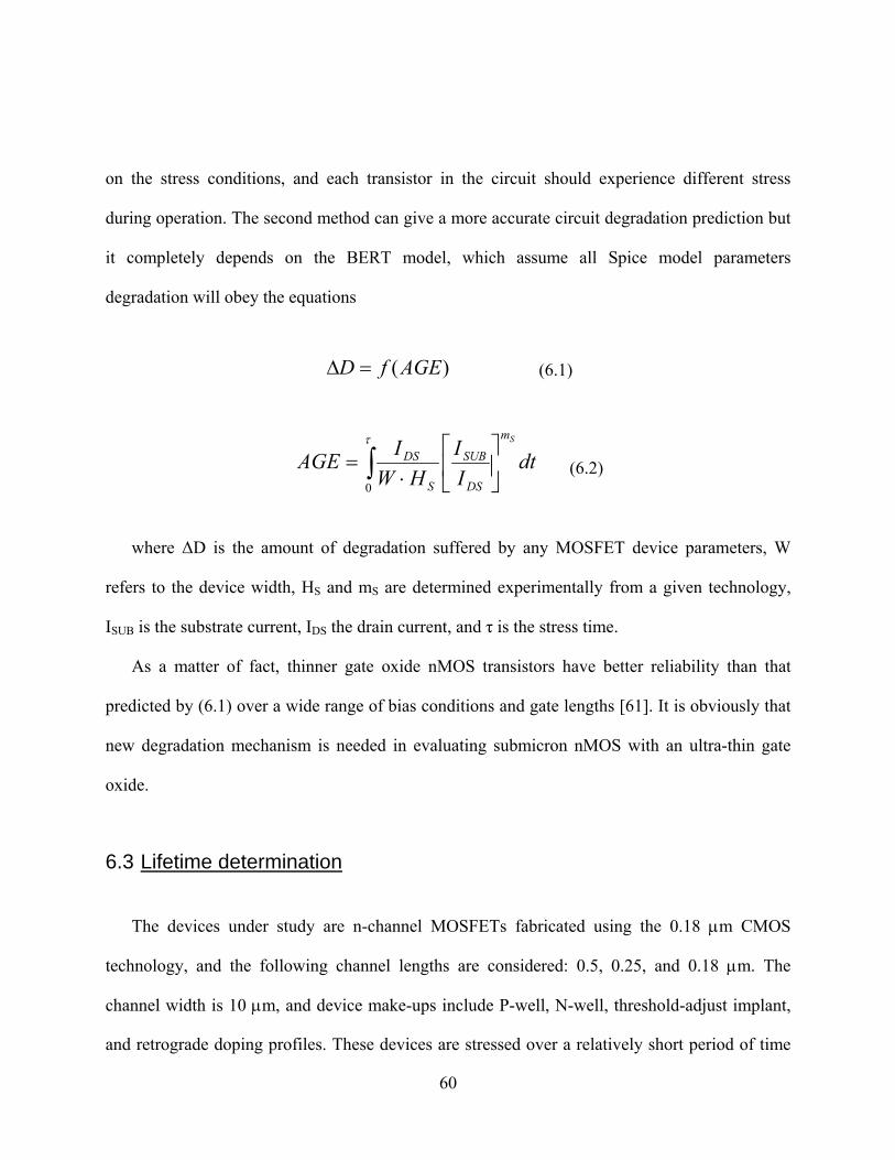
60
on the stress conditions, and each transistor in the circuit should experience different stress
during operation. The second method can give a more accurate circuit degradation prediction but
it completely depends on the BERT model, which assume all Spice model parameters
degradation will obey the equations
)(AGEfD =Δ (6.1)
∫ ⎥⎦
⎤⎢⎣
⎡⋅
=τ
0
dtII
HWIAGE
Sm
DS
SUB
S
DS (6.2)
where ΔD is the amount of degradation suffered by any MOSFET device parameters, W
refers to the device width, HS and mS are determined experimentally from a given technology,
ISUB is the substrate current, IDS the drain current, and τ is the stress time.
As a matter of fact, thinner gate oxide nMOS transistors have better reliability than that
predicted by (6.1) over a wide range of bias conditions and gate lengths [61]. It is obviously that
new degradation mechanism is needed in evaluating submicron nMOS with an ultra-thin gate
oxide.
6.3 Lifetime determination
The devices under study are n-channel MOSFETs fabricated using the 0.18 μm CMOS
technology, and the following channel lengths are considered: 0.5, 0.25, and 0.18 μm. The
channel width is 10 μm, and device make-ups include P-well, N-well, threshold-adjust implant,
and retrograde doping profiles. These devices are stressed over a relatively short period of time
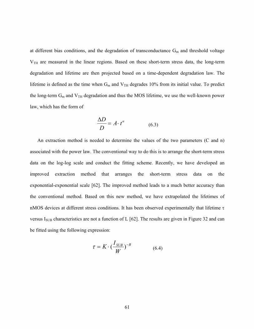
61
at different bias conditions, and the degradation of transconductance Gm and threshold voltage
VTH are measured in the linear regions. Based on these short-term stress data, the long-term
degradation and lifetime are then projected based on a time-dependent degradation law. The
lifetime is defined as the time when Gm and VTH degrades 10% from its initial value. To predict
the long-term Gm and VTH degradation and thus the MOS lifetime, we use the well-known power
law, which has the form of
ntADD
⋅=Δ
(6.3)
An extraction method is needed to determine the values of the two parameters (C and n)
associated with the power law. The conventional way to do this is to arrange the short-term stress
data on the log-log scale and conduct the fitting scheme. Recently, we have developed an
improved extraction method that arranges the short-term stress data on the
exponential-exponential scale [62]. The improved method leads to a much better accuracy than
the conventional method. Based on this new method, we have extrapolated the lifetimes of
nMOS devices at different stress conditions. It has been observed experimentally that lifetime τ
versus ISUB characteristics are not a function of L [62]. The results are given in Figure 32 and can
be fitted using the following expression:
BSUB
WIK −⋅= )(τ (6.4)
62
10-6 10-5
104
105
106
107
10/0.18 10/0.25 10/0.5 linear fit
Lifetime=4.312x10⁻⁵xIB-1.91898
Life
time
(s)
ISUB (A)
Figure 32 Transconductance lifetime versus substrate current obtained from measurements
and fitting.
10-5
104
105
10/0.18 10/0.25 linear fit
Lifetime=1.635e-6XISUB-2.1846
Life
time
(s)
ISUB (A)
Figure 33 Threshold voltage lifetime versus substrate current obtained from measurements and fitting.
Similar trend for the lifetime based on the threshold voltage shift can be seen in Figure 33.
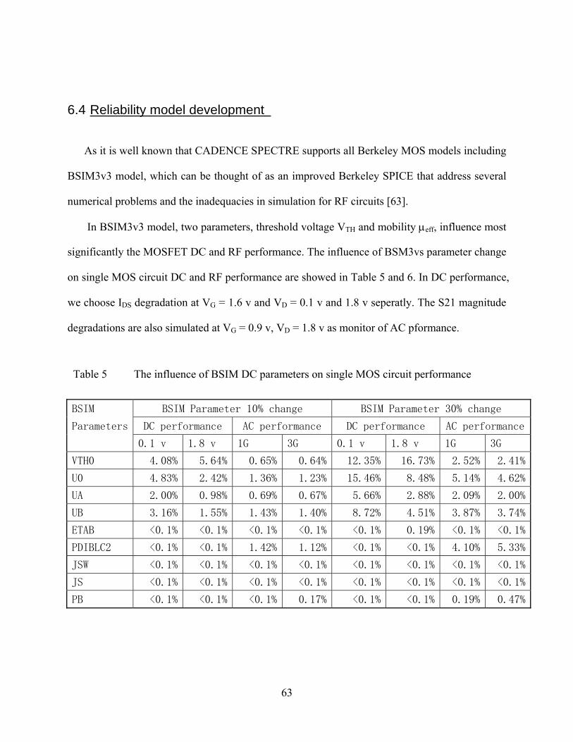
63
6.4 Reliability model development
As it is well known that CADENCE SPECTRE supports all Berkeley MOS models including
BSIM3v3 model, which can be thought of as an improved Berkeley SPICE that address several
numerical problems and the inadequacies in simulation for RF circuits [63].
In BSIM3v3 model, two parameters, threshold voltage VTH and mobility μeff, influence most
significantly the MOSFET DC and RF performance. The influence of BSM3vs parameter change
on single MOS circuit DC and RF performance are showed in Table 5 and 6. In DC performance,
we choose IDS degradation at VG = 1.6 v and VD = 0.1 v and 1.8 v seperatly. The S21 magnitude
degradations are also simulated at VG = 0.9 v, VD = 1.8 v as monitor of AC pformance.
Table 5 The influence of BSIM DC parameters on single MOS circuit performance BSIM BSIM Parameter 10% change BSIM Parameter 30% change
Parameters DC performance AC performance DC performance AC performance
0.1 v 1.8 v 1G 3G 0.1 v 1.8 v 1G 3G
VTH0 4.08% 5.64% 0.65% 0.64% 12.35% 16.73% 2.52% 2.41%
U0 4.83% 2.42% 1.36% 1.23% 15.46% 8.48% 5.14% 4.62%
UA 2.00% 0.98% 0.69% 0.67% 5.66% 2.88% 2.09% 2.00%
UB 3.16% 1.55% 1.43% 1.40% 8.72% 4.51% 3.87% 3.74%
ETAB <0.1% <0.1% <0.1% <0.1% <0.1% 0.19% <0.1% <0.1%
PDIBLC2 <0.1% <0.1% 1.42% 1.12% <0.1% <0.1% 4.10% 5.33%
JSW <0.1% <0.1% <0.1% <0.1% <0.1% <0.1% <0.1% <0.1%
JS <0.1% <0.1% <0.1% <0.1% <0.1% <0.1% <0.1% <0.1%
PB <0.1% <0.1% <0.1% 0.17% <0.1% <0.1% 0.19% 0.47%
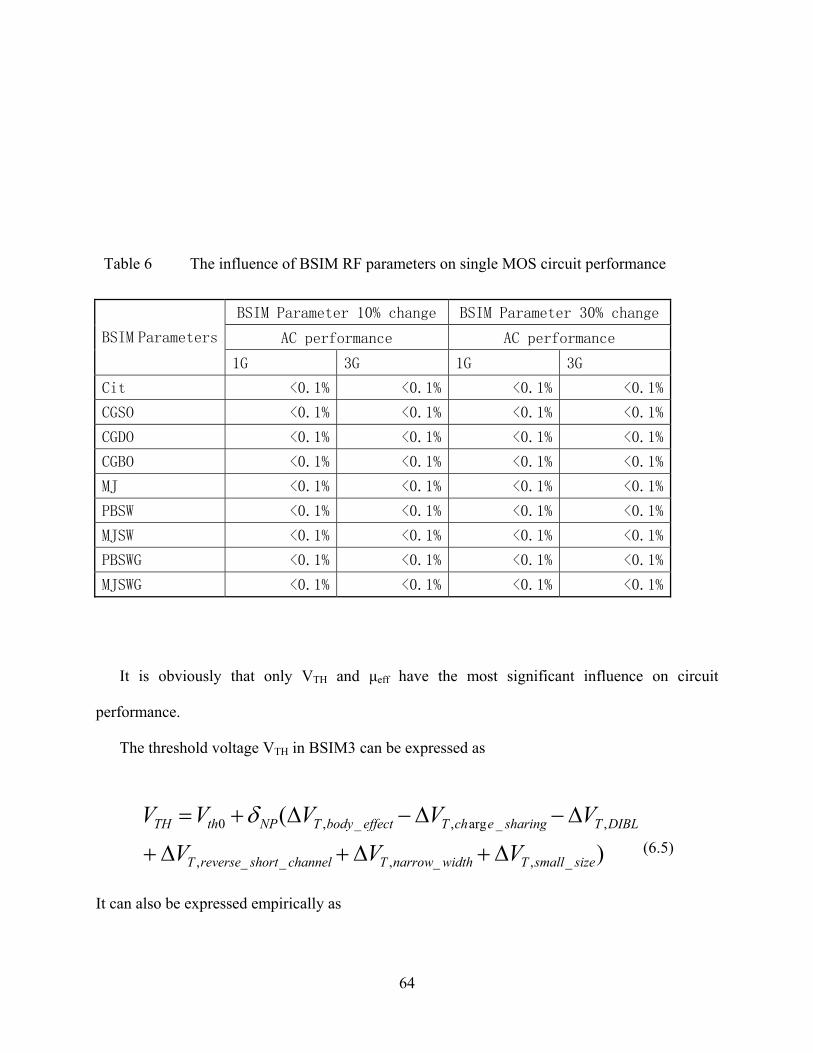
64
Table 6 The influence of BSIM RF parameters on single MOS circuit performance
BSIM Parameter 10% change BSIM Parameter 30% change
AC performance AC performance BSIM Parameters
1G 3G 1G 3G
Cit <0.1% <0.1% <0.1% <0.1%
CGSO <0.1% <0.1% <0.1% <0.1%
CGDO <0.1% <0.1% <0.1% <0.1%
CGBO <0.1% <0.1% <0.1% <0.1%
MJ <0.1% <0.1% <0.1% <0.1%
PBSW <0.1% <0.1% <0.1% <0.1%
MJSW <0.1% <0.1% <0.1% <0.1%
PBSWG <0.1% <0.1% <0.1% <0.1%
MJSWG <0.1% <0.1% <0.1% <0.1%
It is obviously that only VTH and μeff have the most significant influence on circuit
performance.
The threshold voltage VTH in BSIM3 can be expressed as
)(
_,_,__,
,_arg,_,0
sizesmallTwidthnarrowTchannelshortreverseT
DIBLTsharingechTeffectbodyTNPthTH
VVVVVVVV
Δ+Δ+Δ+
Δ−Δ−Δ+= δ (6.5)
It can also be expressed empirically as
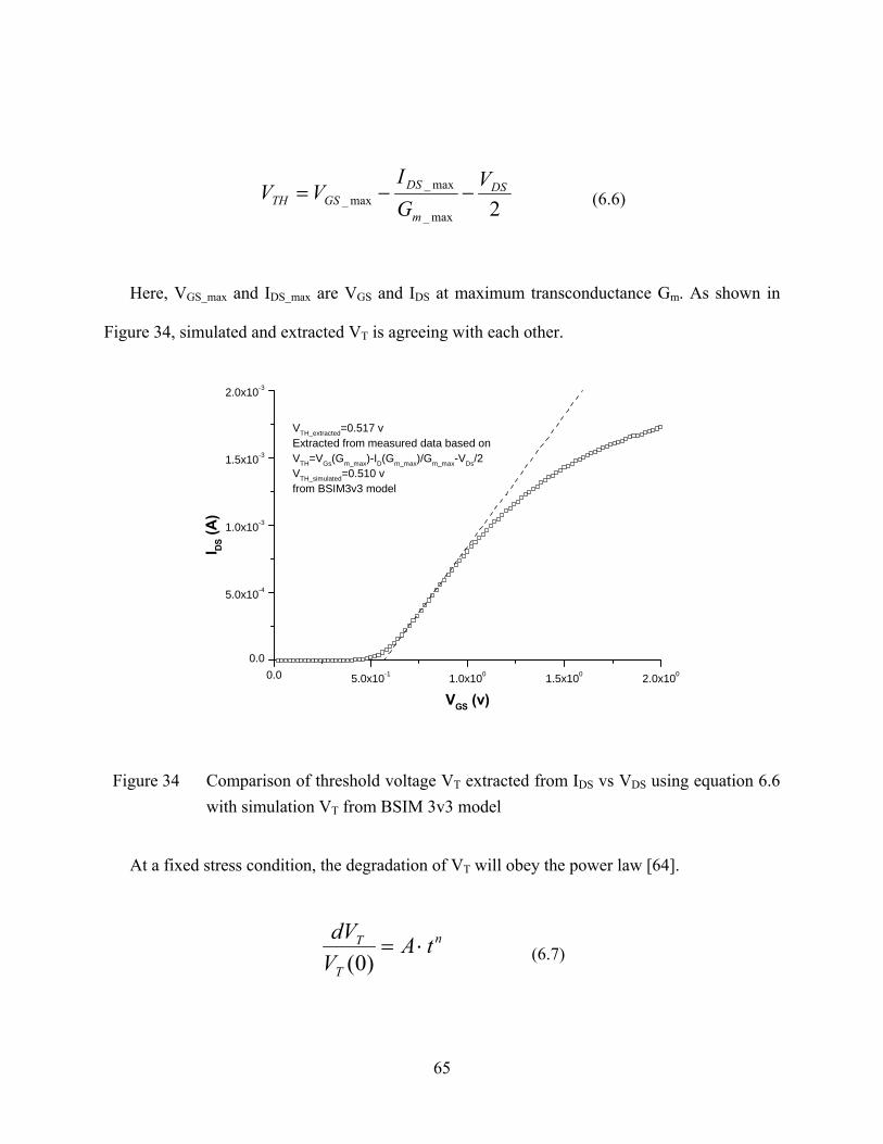
65
2max_
max_max_
DS
m
DSGSTH
VGI
VV −−= (6.6)
Here, VGS_max and IDS_max are VGS and IDS at maximum transconductance Gm. As shown in
Figure 34, simulated and extracted VT is agreeing with each other.
0.0 5.0x10⁻¹ 1.0x100 1.5x100 2.0x100
0.0
5.0x10⁻⁴
1.0x10⁻³
1.5x10⁻³
2.0x10⁻³
VTH_extracted=0.517 vExtracted from measured data based onVTH=VGs(Gm_max)-ID(Gm_max)/Gm_max-VDs/2VTH_simulated=0.510 vfrom BSIM3v3 model
I DS (
A)
VGS (v)
Figure 34 Comparison of threshold voltage VT extracted from IDS vs VDS using equation 6.6
with simulation VT from BSIM 3v3 model
At a fixed stress condition, the degradation of VT will obey the power law [64].
n
T
T tAVdV
⋅=)0( (6.7)
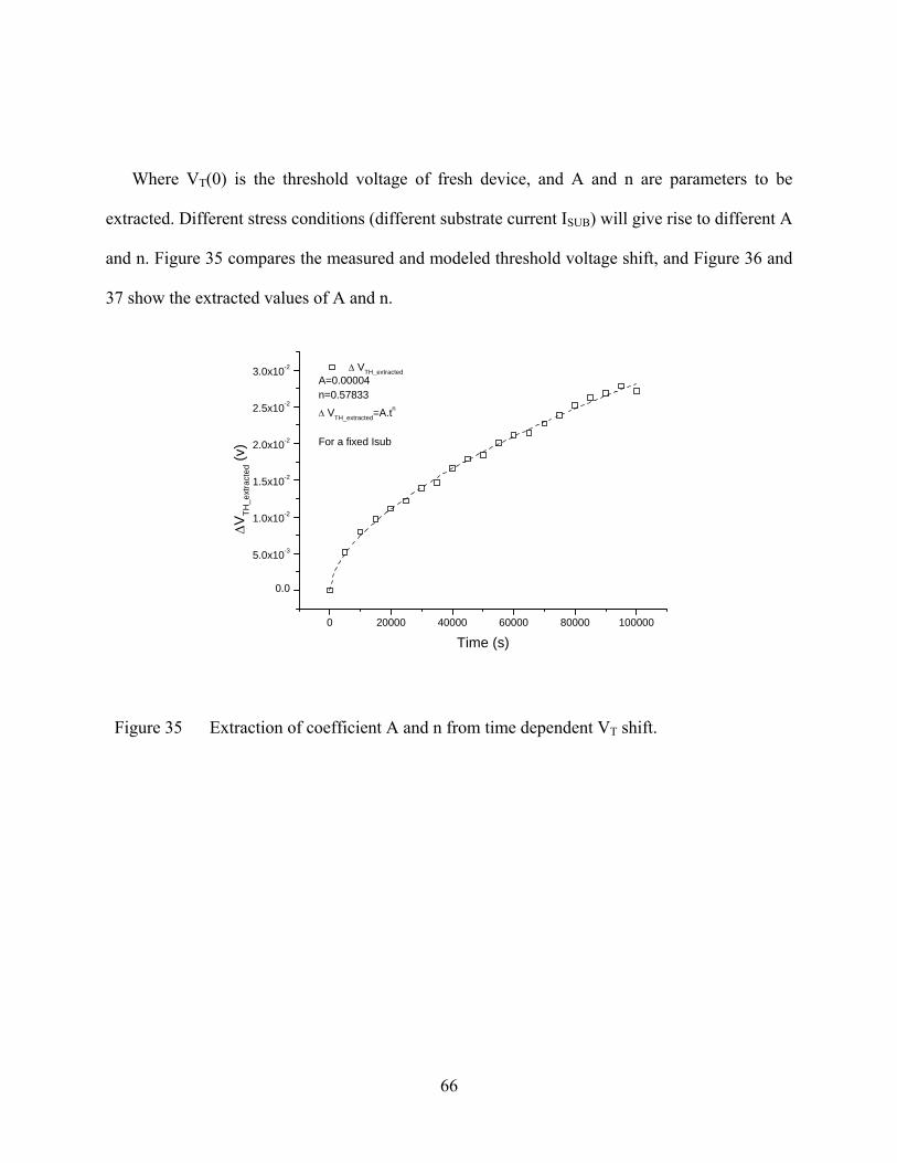
66
Where VT(0) is the threshold voltage of fresh device, and A and n are parameters to be
extracted. Different stress conditions (different substrate current ISUB) will give rise to different A
and n. Figure 35 compares the measured and modeled threshold voltage shift, and Figure 36 and
37 show the extracted values of A and n.
0 20000 40000 60000 80000 100000
0.0
5.0x10⁻³
1.0x10⁻²
1.5x10⁻²
2.0x10⁻²
2.5x10⁻²
3.0x10⁻² Δ VTH_extractedA=0.00004n=0.57833
Δ VTH_extracted=A.tn
For a fixed Isub
ΔVTH
_ext
ract
ed (v
)
Time (s)
Figure 35 Extraction of coefficient A and n from time dependent VT shift.

67
2.0x10⁻⁶ 4.0x10⁻⁶ 6.0x10⁻⁶ 8.0x10⁻⁶ 1.0x10⁻⁵ 1.2x10⁻⁵ 1.4x10⁻⁵ 1.6x10⁻⁵ 1.8x10⁻⁵
0.0
2.0x10⁻⁵
4.0x10⁻⁵
6.0x10⁻⁵
8.0x10⁻⁵
1.0x10⁻⁴
1.2x10⁻⁴
1.4x10⁻⁴
1.6x10⁻⁴
1.8x10⁻⁴
Coefficient A
A=1191.78184.ISUB1.43805
Coe
ffici
ent A
ISUb (A)
Figure 36 Fitting data of VT coefficient A at different substrate current ISUB.
2.0x10⁻⁶ 4.0x10⁻⁶ 6.0x10⁻⁶ 8.0x10⁻⁶ 1.0x10⁻⁵ 1.2x10⁻⁵ 1.4x10⁻⁵ 1.6x10⁻⁵ 1.8x10⁻⁵
0.0
0.1
0.2
0.3
0.4
0.5
0.6
Coefficient nAverage Value=0.572346
Coe
ffici
ent n
ISUB (A)
Figure 37 Fitting data of VT coefficient n at different substrate current ISUB.
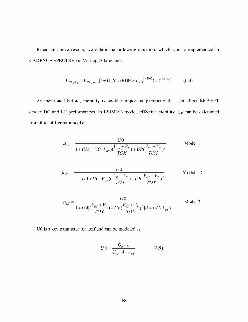
68
Based on above results, we obtain the following equation, which can be implemented in
CADENCE SPECTRE via Verilog-A language,
])1191.78184(1[ 58747.043805.1_deg_ tIVV SUBfreshTHTH ××+= (6.8)
As mentioned before, mobility is another important parameter that can affect MOSFET
device DC and RF performances. In BSIM3v3 model, effective mobility μeff can be calculated
from three different models:
2)())((1
0
TOXVVUB
TOXVVVUCUA
UTGSTGS
BS
eff ++
+⋅++
=μ Model 1
2)())((1
0
TOXVVUB
TOXVVVUCUA
UTGSTGS
BS
eff −+
−⋅++
=μ Model 2
)1]()()[(1
02
BSTGSTGS
eff
VUCTOX
VVUBTOX
VVUA
U
⋅++
++
+=μ Model 3
U0 is a key parameter for μeff and can be modeled as
DSox
m
VWCLGU⋅⋅⋅
=0 (6.9)

69
As shown in Figure 38, we can use equation 6.9 to extract U0 from transcanductance
experiment data and implement it into μeff in BSIM 3v3 model equation. Figure 39 shows the
calculated mobility degradation and Figure 40 and 41 show the extracted A and n coefficients.
0 2
0.0
5.0x10⁻⁴
1.0x10⁻³
1.5x10⁻³
2.0x10⁻³
VG (v)
Gm
(A/v
)
0
100
200
300
400
Mobility (cm
2/v.s)
U0_extracted=4.26187E+02Extract from measured databased on U0=Gm*L/(Cox*W*VDS)
U0_simulation=4.387662E+02Simulated from BSIM3v3
Figure 38 Comparison of mobility U0 extracted from Gm vs VG using equation 6.9 with simulation U0 from BSIM 3v3 model.
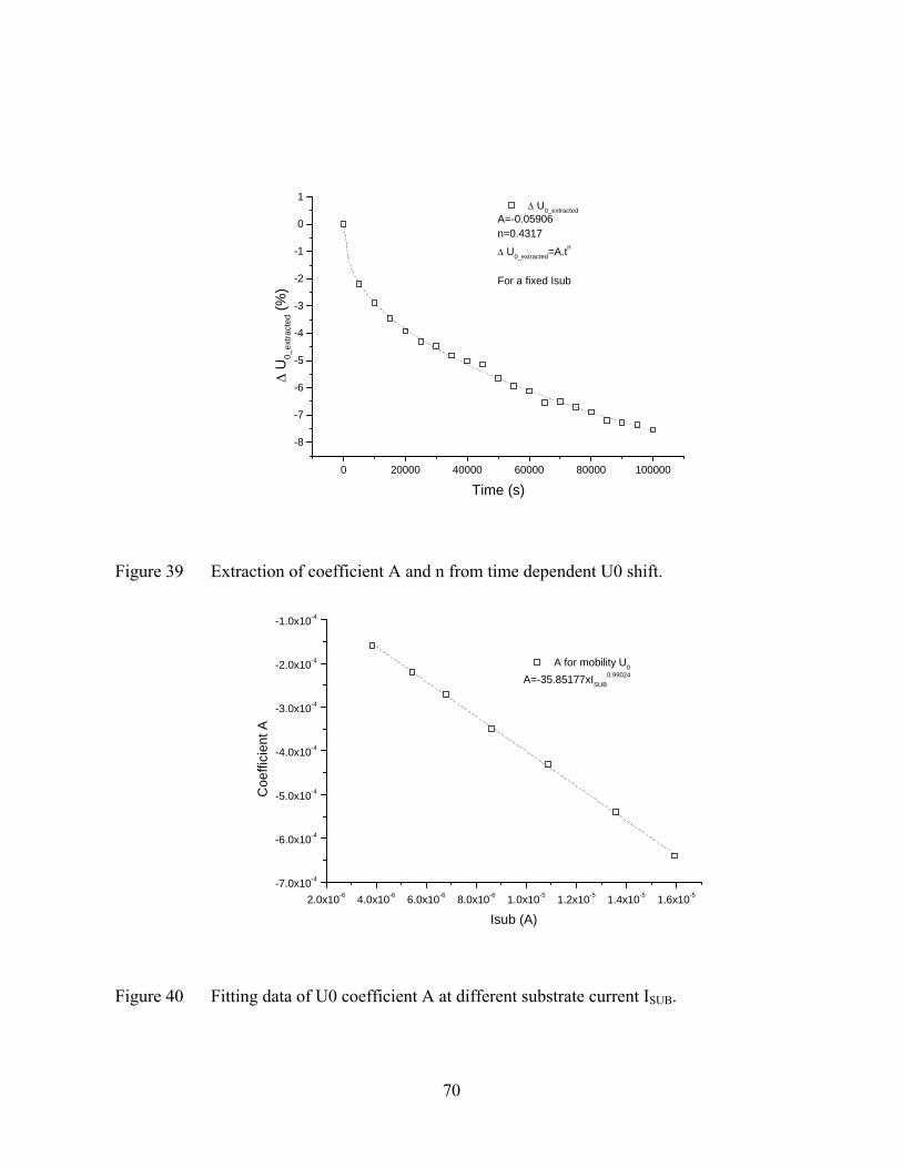
70
0 20000 40000 60000 80000 100000
-8
-7
-6
-5
-4
-3
-2
-1
0
1 Δ U0_extracted
A=-0.05906n=0.4317
Δ U0_extracted=A.tn
For a fixed IsubΔ
U0_
extra
cted
(%)
Time (s)
Figure 39 Extraction of coefficient A and n from time dependent U0 shift.
2.0x10⁻⁶ 4.0x10⁻⁶ 6.0x10⁻⁶ 8.0x10⁻⁶ 1.0x10⁻⁵ 1.2x10⁻⁵ 1.4x10⁻⁵ 1.6x10⁻⁵-7.0x10⁻⁴
-6.0x10⁻⁴
-5.0x10⁻⁴
-4.0x10⁻⁴
-3.0x10⁻⁴
-2.0x10⁻⁴
-1.0x10⁻⁴
A for mobility U0
A=-35.85177xISUB0.99024
Coe
ffici
ent A
Isub (A)
Figure 40 Fitting data of U0 coefficient A at different substrate current ISUB.
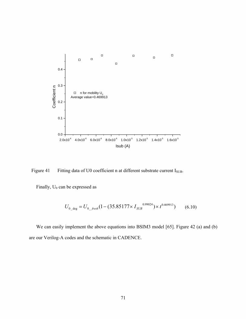
71
2.0x10⁻⁶ 4.0x10⁻⁶ 6.0x10⁻⁶ 8.0x10⁻⁶ 1.0x10⁻⁵ 1.2x10⁻⁵ 1.4x10⁻⁵ 1.6x10⁻⁵
0.0
0.1
0.2
0.3
0.4
n for mobility U0Average value=0.469913
Coe
ffici
ent n
Isub (A)
Figure 41 Fitting data of U0 coefficient n at different substrate current ISUB.
Finally, U0 can be expressed as
))85177.35(1( 469913.099024.0_0deg_0 tIUU SUBfresh ××−= (6.10)
We can easily implement the above equations into BSIM3 model [65]. Figure 42 (a) and (b)
are our Verilog-A codes and the schematic in CADENCE.
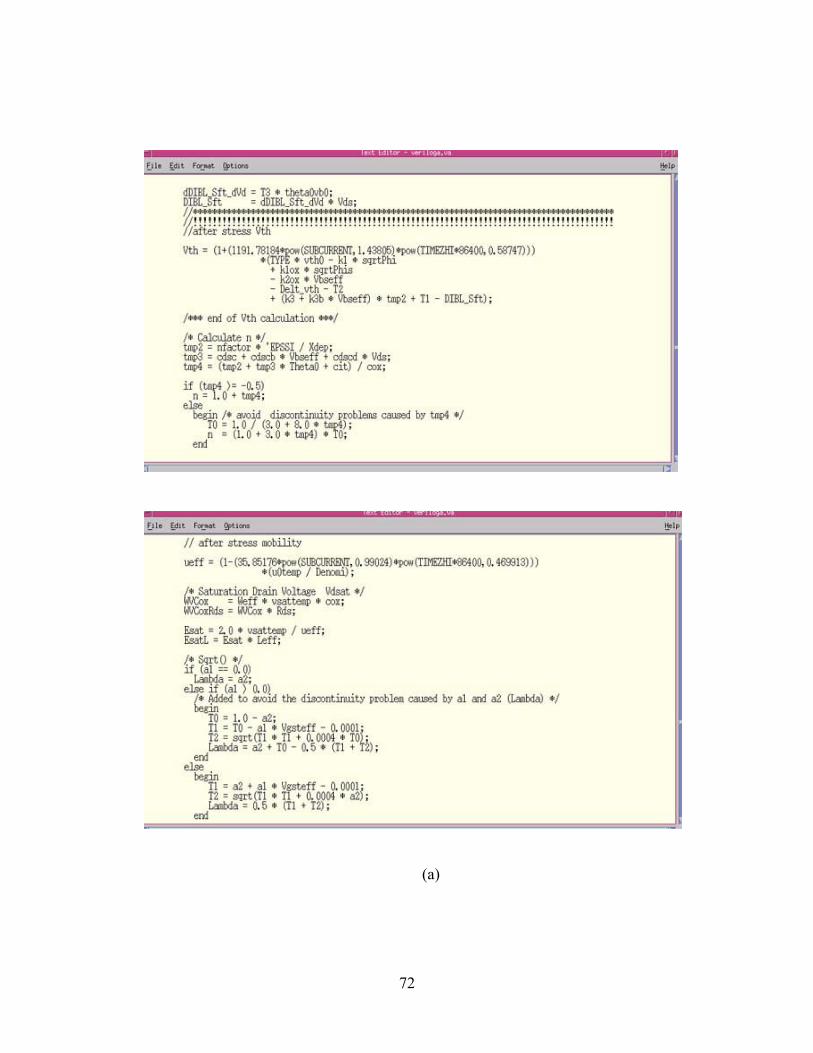
72
(a)
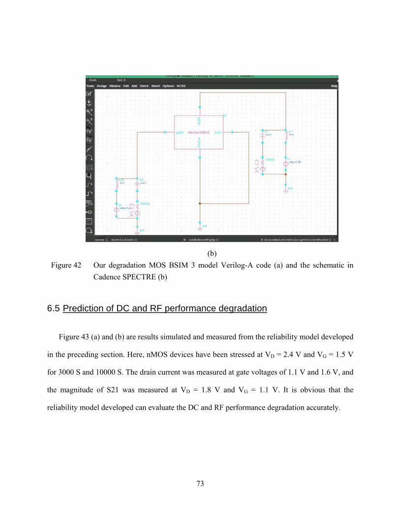
73
(b) Figure 42 Our degradation MOS BSIM 3 model Verilog-A code (a) and the schematic in
Cadence SPECTRE (b)
6.5 Prediction of DC and RF performance degradation
Figure 43 (a) and (b) are results simulated and measured from the reliability model developed
in the preceding section. Here, nMOS devices have been stressed at VD = 2.4 V and VG = 1.5 V
for 3000 S and 10000 S. The drain current was measured at gate voltages of 1.1 V and 1.6 V, and
the magnitude of S21 was measured at VD = 1.8 V and VG = 1.1 V. It is obvious that the
reliability model developed can evaluate the DC and RF performance degradation accurately.
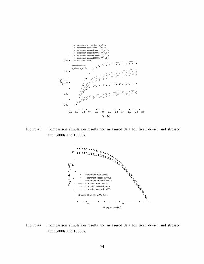
74
-0.2 0.0 0.2 0.4 0.6 0.8 1.0 1.2 1.4 1.6 1.8 2.0
0.00
0.02
0.04
0.06
0.08
experiment fresh device VG=1.1 v experiment fresh device VG=1.6 v experiment stressed 3000s VG=1.1 v experiment stressed 3000s VG=1.6 v experiment stressed 10000s VG=1.1 v experiment stressed 10000s VG=1.6 v simulation results
stress conditions:VD=2.4 v, VG=1.5 v
I D (v)
V D (v)
Figure 43 Comparison simulation results and measured data for fresh device and stressed after 3000s and 10000s.
1E9 1E10
0
5
10
15
experiment fresh device experiment stressed 3000s experiment stressed 10000s simulation fresh device simulation stressed 3000s simulation stressed 10000s
stressed @ Vd=2.4 v, Vg=1.5 v
Mag
nitu
de S
21 (
dB)
Frequency (Hz)
Figure 44 Comparison simulation results and measured data for fresh device and stressed after 3000s and 10000s.
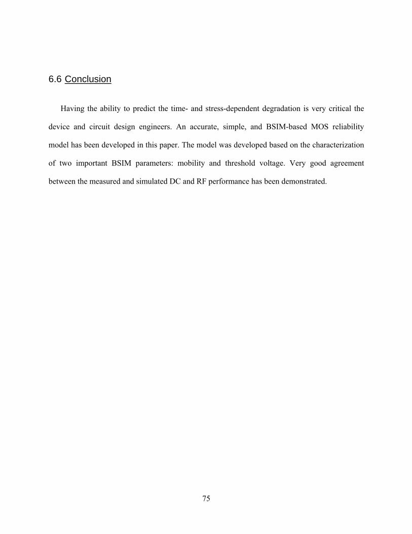
75
6.6 Conclusion
Having the ability to predict the time- and stress-dependent degradation is very critical the
device and circuit design engineers. An accurate, simple, and BSIM-based MOS reliability
model has been developed in this paper. The model was developed based on the characterization
of two important BSIM parameters: mobility and threshold voltage. Very good agreement
between the measured and simulated DC and RF performance has been demonstrated.
76
APPENDIX: VERILOG-A CODE
77
/*****************************************************************/
/* Berkeley BSIM3v3.2.0 & BSIM3v3.2.4 (default) Verilog-A model */
/*****************************************************************/
// UPDATED March 19 2004
// Contributed By:
// Geoffrey Coram, Ph.D Senior CAD Engineer Analog Devices, Inc.
// Edited By
// Zhi Cui, Ph.D University of Central Florida
`define VOLTAGE_MAXDELTA 0.3
`include "discipline.h"
// Following line must be uncomment for using NQS charge model (NQSMOD=1)
//`define NQSMOD
//****** Physical constants ******//
`define EPSOX 3.453133e-11
`define KboQ 8.617087e-5
`define EPSSI 1.03594e-10
`define Charge_q 1.60219e-19
`define CONSTvt0 0.02586419
`define CONSTroot2 1.41421356
//****** Mathematical constants and constants of limitation ******//
`define PI 3.141592654
`define EXP_THRESHOLD 34.0
`define MIN_EXP 1.713908431e-15
`define MAX_EXP 5.834617425e14
// //****** Constants for the model ******//
`define DELTA_1 0.02
`define DELTA_3 0.02
`define DELTA_4 0.02
module a_mos_18_10(drain, gate, source, bulk);
inout drain, gate, source, bulk;
electrical drain, gate, source, bulk;
electrical drainp, sourcep; // internal nodes
`ifdef NQSMOD
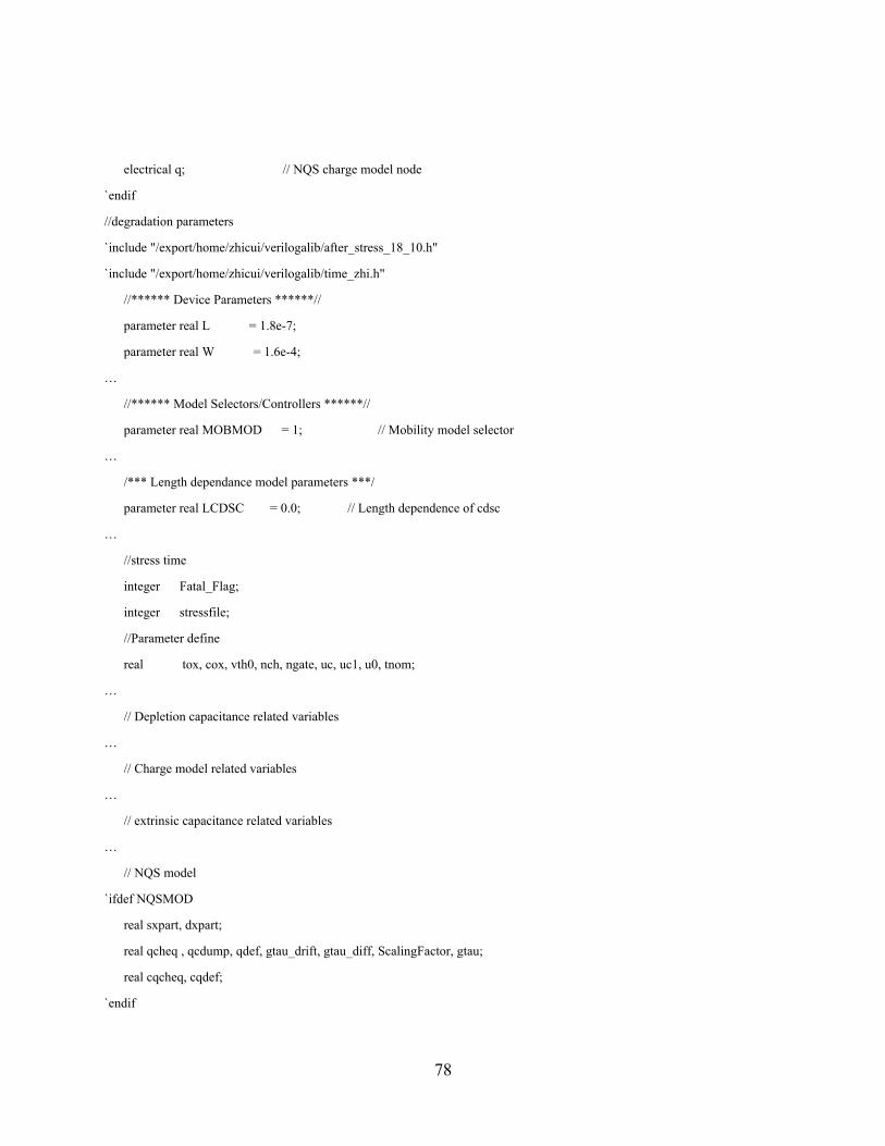
78
electrical q; // NQS charge model node
`endif
//degradation parameters
`include "/export/home/zhicui/verilogalib/after_stress_18_10.h"
`include "/export/home/zhicui/verilogalib/time_zhi.h"
//****** Device Parameters ******//
parameter real L = 1.8e-7;
parameter real W = 1.6e-4;
…
//****** Model Selectors/Controllers ******//
parameter real MOBMOD = 1; // Mobility model selector
…
/*** Length dependance model parameters ***/
parameter real LCDSC = 0.0; // Length dependence of cdsc
…
//stress time
integer Fatal_Flag;
integer stressfile;
//Parameter define
real tox, cox, vth0, nch, ngate, uc, uc1, u0, tnom;
…
// Depletion capacitance related variables
…
// Charge model related variables
…
// extrinsic capacitance related variables
…
// NQS model
`ifdef NQSMOD
real sxpart, dxpart;
real qcheq , qcdump, qdef, gtau_drift, gtau_diff, ScalingFactor, gtau;
real cqcheq, cqdef;
`endif
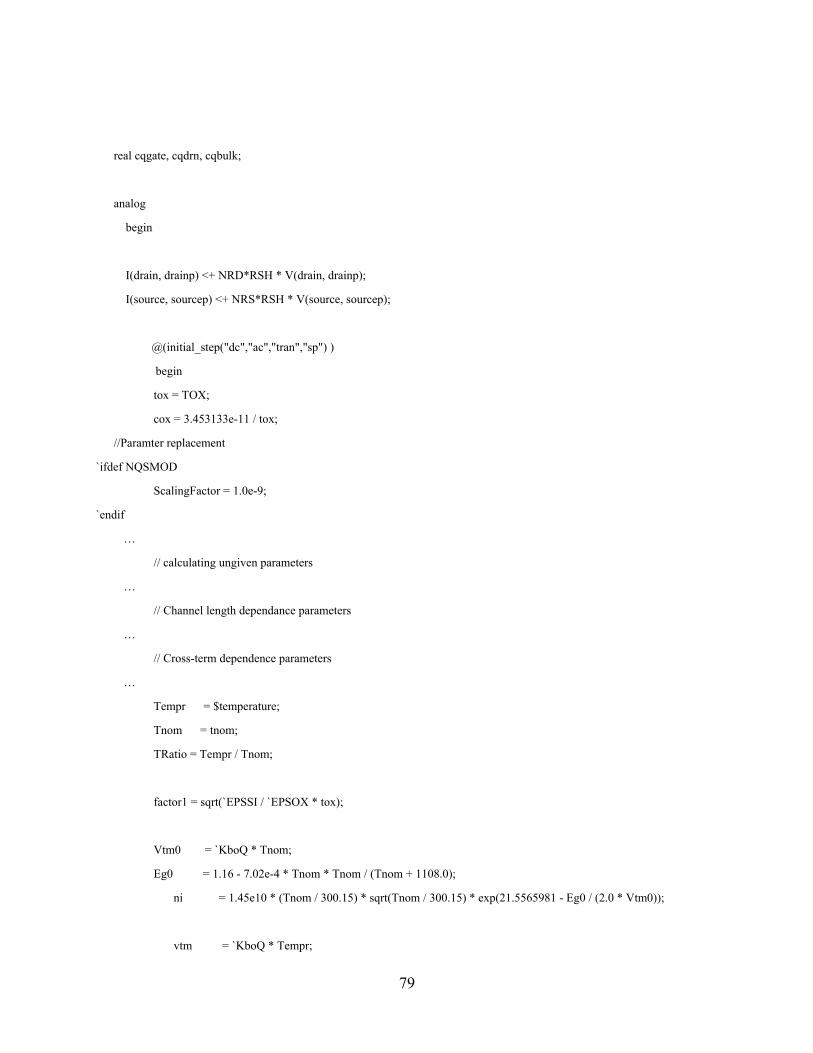
79
real cqgate, cqdrn, cqbulk;
analog
begin
I(drain, drainp) <+ NRD*RSH * V(drain, drainp);
I(source, sourcep) <+ NRS*RSH * V(source, sourcep);
@(initial_step("dc","ac","tran","sp") )
begin
tox = TOX;
cox = 3.453133e-11 / tox;
//Paramter replacement
`ifdef NQSMOD
ScalingFactor = 1.0e-9;
`endif
…
// calculating ungiven parameters
…
// Channel length dependance parameters
…
// Cross-term dependence parameters
…
Tempr = $temperature;
Tnom = tnom;
TRatio = Tempr / Tnom;
factor1 = sqrt(`EPSSI / `EPSOX * tox);
Vtm0 = `KboQ * Tnom;
Eg0 = 1.16 - 7.02e-4 * Tnom * Tnom / (Tnom + 1108.0);
ni = 1.45e10 * (Tnom / 300.15) * sqrt(Tnom / 300.15) * exp(21.5565981 - Eg0 / (2.0 * Vtm0));
vtm = `KboQ * Tempr;
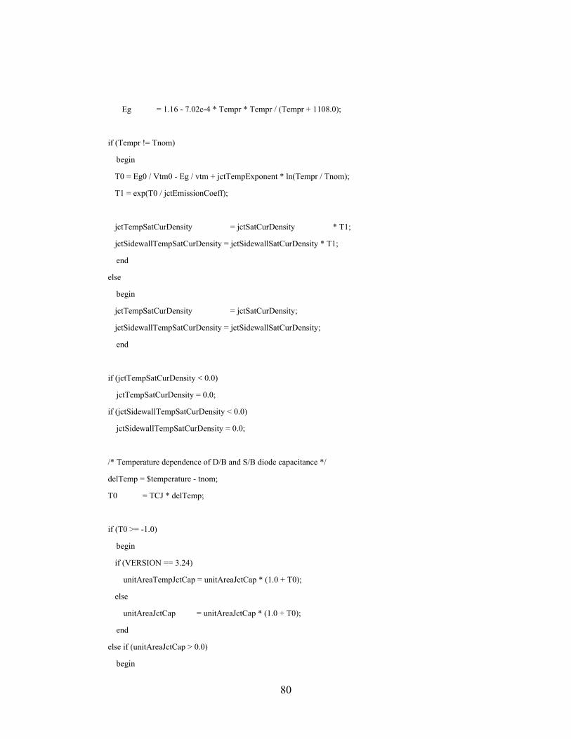
80
Eg = 1.16 - 7.02e-4 * Tempr * Tempr / (Tempr + 1108.0);
if (Tempr != Tnom)
begin
T0 = Eg0 / Vtm0 - Eg / vtm + jctTempExponent * ln(Tempr / Tnom);
T1 = exp(T0 / jctEmissionCoeff);
jctTempSatCurDensity = jctSatCurDensity * T1;
jctSidewallTempSatCurDensity = jctSidewallSatCurDensity * T1;
end
else
begin
jctTempSatCurDensity = jctSatCurDensity;
jctSidewallTempSatCurDensity = jctSidewallSatCurDensity;
end
if (jctTempSatCurDensity < 0.0)
jctTempSatCurDensity = 0.0;
if (jctSidewallTempSatCurDensity < 0.0)
jctSidewallTempSatCurDensity = 0.0;
/* Temperature dependence of D/B and S/B diode capacitance */
delTemp = $temperature - tnom;
T0 = TCJ * delTemp;
if (T0 >= -1.0)
begin
if (VERSION == 3.24)
unitAreaTempJctCap = unitAreaJctCap * (1.0 + T0);
else
unitAreaJctCap = unitAreaJctCap * (1.0 + T0);
end
else if (unitAreaJctCap > 0.0)
begin
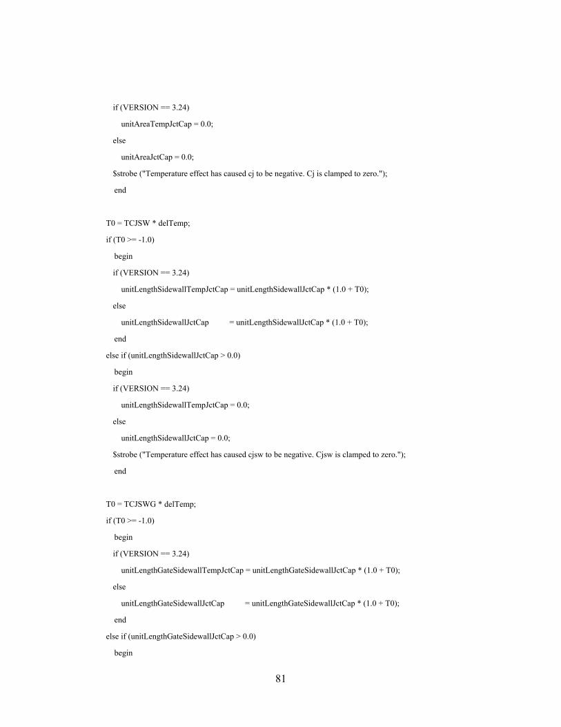
81
if (VERSION == 3.24)
unitAreaTempJctCap = 0.0;
else
unitAreaJctCap = 0.0;
$strobe ("Temperature effect has caused cj to be negative. Cj is clamped to zero.");
end
T0 = TCJSW * delTemp;
if (T0 >= -1.0)
begin
if (VERSION == 3.24)
unitLengthSidewallTempJctCap = unitLengthSidewallJctCap * (1.0 + T0);
else
unitLengthSidewallJctCap = unitLengthSidewallJctCap * (1.0 + T0);
end
else if (unitLengthSidewallJctCap > 0.0)
begin
if (VERSION == 3.24)
unitLengthSidewallTempJctCap = 0.0;
else
unitLengthSidewallJctCap = 0.0;
$strobe ("Temperature effect has caused cjsw to be negative. Cjsw is clamped to zero.");
end
T0 = TCJSWG * delTemp;
if (T0 >= -1.0)
begin
if (VERSION == 3.24)
unitLengthGateSidewallTempJctCap = unitLengthGateSidewallJctCap * (1.0 + T0);
else
unitLengthGateSidewallJctCap = unitLengthGateSidewallJctCap * (1.0 + T0);
end
else if (unitLengthGateSidewallJctCap > 0.0)
begin
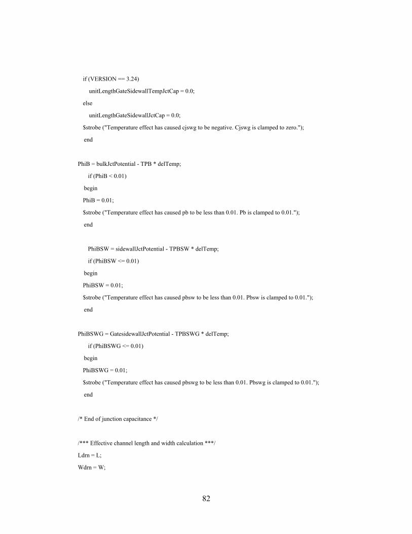
82
if (VERSION == 3.24)
unitLengthGateSidewallTempJctCap = 0.0;
else
unitLengthGateSidewallJctCap = 0.0;
$strobe ("Temperature effect has caused cjswg to be negative. Cjswg is clamped to zero.");
end
PhiB = bulkJctPotential - TPB * delTemp;
if (PhiB < 0.01)
begin
PhiB = 0.01;
$strobe ("Temperature effect has caused pb to be less than 0.01. Pb is clamped to 0.01.");
end
PhiBSW = sidewallJctPotential - TPBSW * delTemp;
if (PhiBSW <= 0.01)
begin
PhiBSW = 0.01;
$strobe ("Temperature effect has caused pbsw to be less than 0.01. Pbsw is clamped to 0.01.");
end
PhiBSWG = GatesidewallJctPotential - TPBSWG * delTemp;
if (PhiBSWG <= 0.01)
begin
PhiBSWG = 0.01;
$strobe ("Temperature effect has caused pbswg to be less than 0.01. Pbswg is clamped to 0.01.");
end
/* End of junction capacitance */
/*** Effective channel length and width calculation ***/
Ldrn = L;
Wdrn = W;
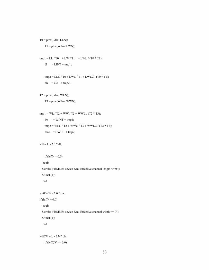
83
T0 = pow(Ldrn, LLN);
T1 = pow(Wdrn, LWN);
tmp1 = LL / T0 + LW / T1 + LWL / (T0 * T1);
dl = LINT + tmp1;
tmp2 = LLC / T0 + LWC / T1 + LWLC / (T0 * T1);
dlc = dlc + tmp2;
T2 = pow(Ldrn, WLN);
T3 = pow(Wdrn, WWN);
tmp1 = WL / T2 + WW / T3 + WWL / (T2 * T3);
dw = WINT + tmp1;
tmp2 = WLC / T2 + WWC / T3 + WWLC / (T2 * T3);
dwc = DWC + tmp2;
leff = L - 2.0 * dl;
if (leff <= 0.0)
begin
$strobe ("BSIM3: device %m: Effective channel length <= 0");
$finish(1);
end
weff = W - 2.0 * dw;
if (leff <= 0.0)
begin
$strobe ("BSIM3: device %m: Effective channel width <= 0");
$finish(1);
end
leffCV = L - 2.0 * dlc;
if (leffCV <= 0.0)
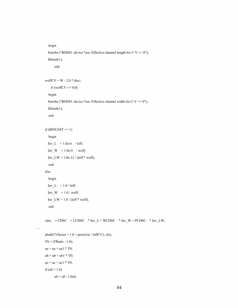
84
begin
$strobe ("BSIM3: device %m: Effective channel length for C-V <= 0");
$finish(1);
end
weffCV = W - 2.0 * dwc;
if (weffCV <= 0.0)
begin
$strobe ("BSIM3: device %m: Effective channel width for C-V <= 0");
$finish(1);
end
if (BINUNIT == 1)
begin
Inv_L = 1.0e-6 / leff;
Inv_W = 1.0e-6 / weff;
Inv_LW = 1.0e-12 / (leff * weff);
end
else
begin
Inv_L = 1.0 / leff;
Inv_W = 1.0 / weff;
Inv_LW = 1.0 / (leff * weff);
end
cdsc = CDSC + LCDSC * Inv_L + WCDSC * Inv_W + PCDSC * Inv_LW;
…
abulkCVfactor = 1.0 + pow((clc / leffCV), cle);
T0 = (TRatio - 1.0);
ua = ua + ua1 * T0;
ub = ub + ub1 * T0;
uc = uc + uc1 * T0;
if (u0 > 1.0)
u0 = u0 / 1.0e4;
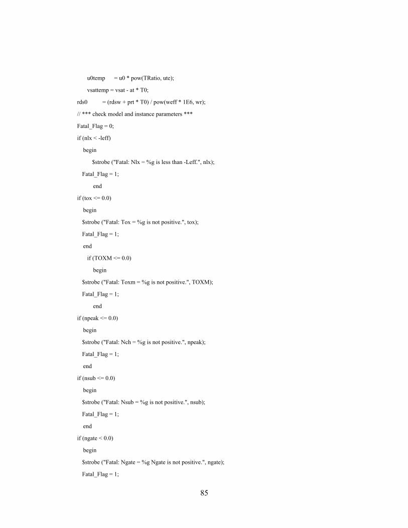
85
u0temp = u0 * pow(TRatio, ute);
vsattemp = vsat - at * T0;
rds0 = (rdsw + prt * T0) / pow(weff * 1E6, wr);
// *** check model and instance parameters ***
Fatal_Flag = 0;
if (nlx < -leff)
begin
$strobe ("Fatal: Nlx = %g is less than -Leff.", nlx);
Fatal_Flag = 1;
end
if (tox <= 0.0)
begin
$strobe ("Fatal: Tox = %g is not positive.", tox);
Fatal_Flag = 1;
end
if (TOXM <= 0.0)
begin
$strobe ("Fatal: Toxm = %g is not positive.", TOXM);
Fatal_Flag = 1;
end
if (npeak <= 0.0)
begin
$strobe ("Fatal: Nch = %g is not positive.", npeak);
Fatal_Flag = 1;
end
if (nsub <= 0.0)
begin
$strobe ("Fatal: Nsub = %g is not positive.", nsub);
Fatal_Flag = 1;
end
if (ngate < 0.0)
begin
$strobe ("Fatal: Ngate = %g Ngate is not positive.", ngate);
Fatal_Flag = 1;
86
end
if (ngate > 1.0e25)
begin
$strobe ("Fatal: Ngate = %g Ngate is too high", ngate);
Fatal_Flag = 1;
end
if (xj <= 0.0)
begin
$strobe ("Fatal: Xj = %g is not positive.", xj);
Fatal_Flag = 1;
end
if (dvt1 < 0.0)
begin
$strobe ("Fatal: Dvt1 = %g is negative.", dvt1);
Fatal_Flag = 1;
end
if (dvt1w < 0.0)
begin
$strobe ("Fatal: Dvt1w = %g is negative.", dvt1w);
Fatal_Flag = 1;
end
if (w0 == -weff)
begin
$strobe ("Fatal: (W0 + Weff) = 0 causing divided-by-zero.");
Fatal_Flag = 1;
end
if (dsub < 0.0)
begin
$strobe ("Fatal: Dsub = %g is negative.", dsub);
Fatal_Flag = 1;
end
if (b1 == -weff)
begin
$strobe ("Fatal: (B1 + Weff) = 0 causing divided-by-zero.");
87
Fatal_Flag = 1;
end
if (u0temp <= 0.0)
begin
$strobe ("Fatal: u0 at current temperature = %g is not positive.", u0temp);
Fatal_Flag = 1;
end
/* Check delta parameter */
if (delta < 0.0)
begin
$strobe ("Fatal: Delta = %g is less than zero.", delta);
Fatal_Flag = 1;
end
if (vsattemp <= 0.0)
begin
$strobe ("Fatal: Vsat at current temperature = %g is not positive.", vsattemp);
Fatal_Flag = 1;
end
/* Check Rout parameters */
if (pclm <= 0.0)
begin
$strobe ("Fatal: Pclm = %g is not positive.", pclm);
Fatal_Flag = 1;
end
if (drout < 0.0)
begin
$strobe ("Fatal: Drout = %g is negative.", drout);
Fatal_Flag = 1;
end
if (pscbe2 <= 0.0)
begin
$strobe ("Warning: Pscbe2 = %g is not positive.", pscbe2);
end
if (unitLengthSidewallJctCap > 0.0 || unitLengthGateSidewallJctCap > 0.0)
88
begin
if (drainPerimeter < weff)
begin
$strobe ("Warning: Pd = %g is less than W.", drainPerimeter);
end
if (sourcePerimeter < weff)
begin
$strobe ("Warning: Ps = %g is less than W.", sourcePerimeter);
end
end
if (noff_param < 0.1)
$strobe ("Warning: Noff = %g is too small.", noff_param);
if (noff_param > 4.0)
$strobe ("Warning: Noff = %g is too large.", noff_param);
if (voffcv_param < -0.5)
$strobe ("Warning: Voffcv = %g is too small.", voffcv_param);
if (voffcv_param > 0.5)
$strobe ("Warning: Voffcv = %g is too large.", voffcv_param);
if (IJTH < 0.0)
begin
$strobe ("Fatal: Ijth = %g cannot be negative.", IJTH);
Fatal_Flag = 1;
end
/* Check capacitance parameters */
if (clc < 0.0)
begin
$strobe ("Fatal: Clc = %g is negative.", clc);
Fatal_Flag = 1;
end
if (moin < 5.0)
$strobe ("Warning: Moin = %g is too small.", moin);
if (moin > 25.0)
$strobe ("Warning: Moin = %g is too large.", moin);
if (((acde < 0.4) && !(VERSION == 3.24)) ||
89
((acde < 0.4) && (VERSION == 3.24) && (CAPMOD == 3.0)))
$strobe ("Warning: Acde = %g is too small.", acde);
if (((acde > 1.6) && !(VERSION == 3.24)) ||
((acde > 1.6) && (VERSION == 3.24) && (CAPMOD == 3.0)))
$strobe ("Warning: Acde = %g is too large.", acde);
// *** end of parameters checking ***
if (PARAMCHK ==1)
begin
/* Check L and W parameters */
if (leff <= 5.0e-8)
$strobe ("Warning: Leff = %g may be too small.", leff);
if (leffCV <= 5.0e-8)
$strobe ("Warning: Leff for CV = %g may be too small.", leffCV);
if (weff <= 1.0e-7)
$strobe ("Warning: Weff = %g may be too small.", weff);
if (weffCV <= 1.0e-7)
$strobe ("Warning: Weff for CV = %g may be too small.", weffCV);
/* Check threshold voltage parameters */
if (nlx < 0.0)
$strobe ("Warning: Nlx = %g is negative.", nlx);
if (tox < 1.0e-9)
$strobe ("Warning: Tox = %g is less than 10A.", tox);
if (npeak <= 1.0e15)
$strobe ("Warning: Nch = %g may be too small.", npeak);
else if (npeak >= 1.0e21)
$strobe ("Warning: Nch = %g may be too large.", npeak);
if (nsub <= 1.0e14)
$strobe ("Warning: Nsub = %g may be too small.", nsub);
else if (nsub >= 1.0e21)
$strobe ("Warning: Nsub = %g may be too large.", nsub);
if ((ngate > 0.0) && (ngate <= 1.0e18))
$strobe ("Warning: Ngate = %g is less than 1.E18cm^-3.", ngate);
if (dvt0 < 0.0)
$strobe ("Warning: Dvt0 = %g is negative.", dvt0);
90
if (abs(1.0e-6 / (w0 + weff)) > 10.0)
$strobe ("Warning: (W0 + Weff) may be too small.");
/* Check subthreshold parameters */
if (nfactor < 0.0)
$strobe ("Warning: Nfactor = %g is negative.", nfactor);
if (cdsc < 0.0)
$strobe ("Warning: Cdsc = %g is negative.", cdsc);
if (cdscd < 0.0)
$strobe ("Warning: Cdscd = %g is negative.", cdscd);
/* Check DIBL parameters */
if (eta0 < 0.0)
$strobe ("Warning: Eta0 = %g is negative.", eta0);
/* Check Abulk parameters */
if (abs(1.0e-6 / (b1 + weff)) > 10.0)
$strobe ("Warning: (B1 + Weff) may be too small.");
/* Check Saturation parameters */
if (a2 < 0.01)
begin
$strobe ("Warning: A2 = %g is too small. Set to 0.01.", a2);
a2 = 0.01;
end
else if (a2 > 1.0)
begin
$strobe ("Warning: A2 = %g is larger than 1. A2 is set to 1 and A1 is set to 0.", a2);
a2 = 1.0;
a1 = 0.0;
end
if (rdsw < 0.0)
begin
$strobe ("Warning: Rdsw = %g is negative. Set to zero.", rdsw);
rdsw = 0.0;
rds0 = 0.0;
end
91
else if ((rds0 > 0.0) && (rds0 < 0.001))
begin
$strobe ("Warning: Rds at current temperature = %g is less than 0.001 ohm. Set to zero.", rds0);
rds0 = 0.0;
end
if (vsattemp < 1.0e3)
$strobe ("Warning: Vsat at current temperature = %g may be too small.", vsattemp);
if (pdibl1 < 0.0)
$strobe ("Warning: Pdibl1 = %g is negative.", pdibl1);
if (pdibl2 < 0.0)
$strobe ("Warning: Pdibl2 = %g is negative.", pdibl2);
/* Check overlap capacitance parameters */
if (cgdo_param < 0.0)
begin
$strobe ("Warning: cgdo = %g is negative. Set to zero.", cgdo_param);
cgdo_param = 0.0;
end
if (cgso_param < 0.0)
begin
$strobe ("Warning: cgso = %g is negative. Set to zero.", cgso_param);
cgso_param = 0.0;
end
if (cgbo_param < 0.0)
begin
$strobe ("Warning: cgbo = %g is negative. Set to zero.", cgbo_param);
cgbo_param = 0.0;
end
end/* loop for the parameter check for warning messages */
if (Fatal_Flag)
$finish(1);
cgdo_param = (cgdo_param + cf) * weffCV;
cgso_param = (cgso_param + cf) * weffCV;
cgbo_param = cgbo_param * leffCV;
T0 = leffCV * leffCV;
92
tconst = u0temp * elm / (cox * weffCV * leffCV * T0);
if ( !npeakGiven && gamma1Given )
begin
T0 = gamma1 * cox;
npeak = 3.021E22 * T0 * T0;
end
phi = 2.0 * Vtm0 * ln(npeak / ni);
sqrtPhi = sqrt(phi);
phis3 = sqrtPhi * phi;
Xdep0 = sqrt(2.0 * `EPSSI / (`Charge_q * npeak * 1.0e6)) * sqrtPhi;
litl = sqrt(3.0 * xj * tox);
vbi = Vtm0 * ln(1.0e20 * npeak / (ni * ni));
cdep0 = sqrt(`Charge_q * `EPSSI * npeak * 1.0e6 / 2.0 / phi);
ldeb = sqrt(`EPSSI * Vtm0 / (`Charge_q * npeak * 1.0e6)) / 3.0;
acde = acde * pow((npeak / 2.0e16), -0.25);
if ( k1Given || k2Given )
begin
if (!k1Given)
begin
$strobe ("Warning: k1 should be specified with k2.");
k1 = 0.53;
end
if (!k2Given)
begin
$strobe ("Warning: k2 should be specified with k1.");
k2 = -0.0186;
end
if (nsubGiven)
$strobe ("Warning: nsub is ignored because k1 or k2 is given.");
if (xtGiven)
$strobe ("Warning: xt is ignored because k1 or k2 is given.");
if (vbxGiven)
$strobe ("Warning: vbx is ignored because k1 or k2 is given.");
if (gamma1Given)

93
$strobe ("Warning: gamma1 is ignored because k1 or k2 is given.");
if (gamma2Given)
$strobe ("Warning: gamma2 is ignored because k1 or k2 is given.");
end
else
begin
if (!vbxGiven)
vbx = phi - 7.7348e-4 * npeak * xt * xt;
if (vbx > 0.0)
vbx = -vbx;
if (vbm > 0.0)
vbm = -vbm;
if (!gamma1Given)
gamma1 = 5.753e-12 * sqrt(npeak) / cox;
if (!gamma2Given)
gamma2 = 5.753e-12 * sqrt(nsub) / cox;
T0 = gamma1 - gamma2;
T1 = sqrt(phi - vbx) - sqrtPhi;
T2 = sqrt(phi * (phi - vbm)) - phi;
k2 = T0 * T1 / (2.0 * T2 + vbm);
k1 = gamma2 - 2.0 * k2 * sqrt(phi - vbm);
end
if (k2 < 0.0)
begin
T0 = 0.5 * k1 / k2;
vbsc = 0.9 * (phi - T0 * T0);
if (vbsc > -3.0)
vbsc = -3.0;
else if (vbsc < -30.0)
vbsc = -30.0;
end
else
vbsc = -30.0;
94
if (vbsc > vbm)
vbsc = vbm;
if (!vfbGiven)
begin
if (vth0Given)
vfb = TYPE * vth0 - phi - k1 * sqrtPhi;
else
vfb = -1.0;
end
if (!vth0Given)
vth0 = TYPE * (vfb + phi + k1 * sqrtPhi);
k1ox = k1 * tox / TOXM;
k2ox = k2 * tox / TOXM;
T1 = sqrt(`EPSSI / `EPSOX * tox * Xdep0);
T0 = exp(-0.5 * dsub * leff / T1);
theta0vb0 = (T0 + 2.0 * T0 * T0);
T0 = exp(-0.5 * drout * leff / T1);
T2 = (T0 + 2.0 * T0 * T0);
thetaRout = pdibl1 * T2 + pdibl2;
/* vfbzb for capMod 1, 2 & 3 */
tmp = sqrt(Xdep0);
tmp1 = vbi - phi;
tmp2 = factor1 * tmp;
T0 = -0.5 * dvt1w * weff * leff / tmp2;
if (T0 > -`EXP_THRESHOLD)
begin
T1 = exp(T0);
T2 = T1 * (1.0 + 2.0 * T1);
end
else
begin
T1 = `MIN_EXP;
T2 = T1 * (1.0 + 2.0 * T1);
end
95
T0 = dvt0w * T2;
T2 = T0 * tmp1;
T0 = -0.5 * dvt1 * leff / tmp2;
if (T0 > -`EXP_THRESHOLD)
begin
T1 = exp(T0);
T3 = T1 * (1.0 + 2.0 * T1);
end
else
begin
T1 = `MIN_EXP;
T3 = T1 * (1.0 + 2.0 * T1);
end
T3 = dvt0 * T3 * tmp1;
T4 = tox * phi / (weff + w0);
T0 = sqrt(1.0 + nlx / leff);
T5 = k1ox * (T0 - 1.0) * sqrtPhi + (kt1 + kt1l / leff) * (TRatio - 1.0);
tmp3 = TYPE * vth0 - T2 - T3 + k3 * T4 + T5;
vfbzb = tmp3 - phi - k1 * sqrtPhi;
// End of vfbzb calculation
// process source/drain series resistance
drainConductance = sheetResistance * drainSquares;
if (drainConductance > 0.0)
drainConductance = 1.0 / drainConductance;
else
drainConductance = 0.0;
sourceConductance = sheetResistance * sourceSquares;
if (sourceConductance > 0.0)
sourceConductance = 1.0 / sourceConductance;
else
sourceConductance = 0.0;
Nvtm = vtm * jctEmissionCoeff;
if ((sourceArea <= 0.0) && (sourcePerimeter <= 0.0))
96
SourceSatCurrent = 1.0e-14;
else
SourceSatCurrent = sourceArea * jctTempSatCurDensity
+ sourcePerimeter * jctSidewallTempSatCurDensity;
if ((SourceSatCurrent > 0.0) && (IJTH > 0.0))
begin
vjsm = Nvtm * ln(IJTH / SourceSatCurrent + 1.0);
if (VERSION == 3.24)
IsEvjsm = SourceSatCurrent * exp(vjsm / Nvtm);
end
if ((drainArea <= 0.0) && (drainPerimeter <= 0.0))
DrainSatCurrent = 1.0e-14;
else
DrainSatCurrent = drainArea * jctTempSatCurDensity
+ drainPerimeter * jctSidewallTempSatCurDensity;
if ((DrainSatCurrent > 0.0) && (IJTH > 0.0))
begin
vjdm = Nvtm * ln(IJTH / DrainSatCurrent + 1.0);
if (VERSION == 3.24)
IsEvjdm = DrainSatCurrent * exp(vjdm / Nvtm);
end
end
//*********************************//
//****** End of initial_step ******//
//*********************************//
vbs = TYPE * V(bulk, sourcep);
vgs = TYPE * V(gate, sourcep);
vds = TYPE * V(drainp, sourcep);
`ifdef NQSMOD
qdef = TYPE * V(q);
`endif
vbd = vbs - vds;
97
vgd = vgs - vds;
vgb = vgs - vbs;
temp = $temperature;
// Source/drain junction diode DC model begins
if (SourceSatCurrent <= 0.0)
begin
gbs = GMIN;
cbs = gbs * vbs;
end
else
begin
if (IJTH == 0.0)
begin
evbs = exp(vbs / Nvtm);
gbs = SourceSatCurrent * evbs / Nvtm + GMIN;
cbs = SourceSatCurrent * (evbs - 1.0) + GMIN * vbs;
end
else
begin
if (vbs < vjsm)
begin
evbs = exp(vbs / Nvtm);
gbs = SourceSatCurrent * evbs / Nvtm + GMIN;
cbs = SourceSatCurrent * (evbs - 1.0) + GMIN * vbs;
end
else
begin
if (VERSION == 3.24)
begin
T0 = IsEvjsm / Nvtm;
cbs = IsEvjsm - SourceSatCurrent
+ GMIN * vbs + T0 * (vbs - vjsm);
98
end
else
begin
T0 = (SourceSatCurrent + IJTH) / Nvtm;
cbs = IJTH + GMIN * vbs + T0 * (vbs - vjsm);
end
gbs = T0 + GMIN;
end
end
end
if (DrainSatCurrent <= 0.0)
begin
gbd = GMIN;
cbd = gbd * vbd;
end
else
begin
if (IJTH == 0.0)
begin
evbd = exp(vbd / Nvtm);
gbd = DrainSatCurrent * evbd / Nvtm + GMIN;
cbd = DrainSatCurrent * (evbd - 1.0) + GMIN * vbd;
end
else
begin
if (vbd < vjdm)
begin
evbd = exp(vbd / Nvtm);
gbd = DrainSatCurrent * evbd / Nvtm + GMIN;
cbd = DrainSatCurrent * (evbd - 1.0) + GMIN * vbd;
end
else
99
begin
if (VERSION == 3.24)
begin
T0 = IsEvjdm / Nvtm;
cbd = IsEvjdm - DrainSatCurrent
+ GMIN * vbd + T0 * (vbd - vjdm);
end
else
begin
T0 = (DrainSatCurrent + IJTH) / Nvtm;
cbd = IJTH + GMIN * vbd + T0 * (vbd - vjdm);
end
gbd = T0 + GMIN;
end
end
end
// End of diode DC model
if (vds >= 0.0)
begin /* normal mode */
mode = 1;
Vds = vds;
Vgs = vgs;
Vbs = vbs;
end
else
begin /* inverse mode */
mode = -1;
Vds = -vds;
Vgs = vgd;
Vbs = vbd;
end
100
T0 = Vbs - vbsc - 0.001;
T1 = sqrt(T0 * T0 - 0.004 * vbsc);
Vbseff = vbsc + 0.5 * (T0 + T1);
// Added to avoid the possible numerical problems due to computer accuracy.
// (See comments for diffVds)
if (Vbseff < Vbs)
Vbseff = Vbs;
if (Vbseff > 0.0)
begin
T0 = phi / (phi + Vbseff);
Phis = phi * T0;
sqrtPhis = phis3 / (phi + 0.5 * Vbseff);
end
else
begin
Phis = phi - Vbseff;
sqrtPhis = sqrt(Phis);
end
Xdep = Xdep0 * sqrtPhis / sqrtPhi;
Leff = leff;
Vtm = vtm;
/*** Vth Calculation ***/
T3 = sqrt(Xdep);
V0 = vbi - phi;
T0 = dvt2 * Vbseff;
if (T0 >= - 0.5)
begin
101
T1 = 1.0 + T0;
T2 = dvt2;
end
else /* Added to avoid any discontinuity problems caused by dvt2 */
begin
T4 = 1.0 / (3.0 + 8.0 * T0);
T1 = (1.0 + 3.0 * T0) * T4;
T2 = dvt2 * T4 * T4;
end
lt1 = factor1 * T3 * T1;
T0 = dvt2w * Vbseff;
if (T0 >= - 0.5)
begin
T1 = 1.0 + T0;
T2 = dvt2w;
end
else /* Added to avoid any discontinuity problems caused by dvt2w */
begin
T4 = 1.0 / (3.0 + 8.0 * T0);
T1 = (1.0 + 3.0 * T0) * T4;
T2 = dvt2w * T4 * T4;
end
ltw = factor1 * T3 * T1;
T0 = -0.5 * dvt1 * Leff / lt1;
if (T0 > -`EXP_THRESHOLD)
begin
T1 = exp(T0);
Theta0 = T1 * (1.0 + 2.0 * T1);
102
end
else
begin
T1 = `MIN_EXP;
Theta0 = T1 * (1.0 + 2.0 * T1);
end
thetavth = dvt0 * Theta0;
Delt_vth = thetavth * V0;
T0 = -0.5 * dvt1w * weff * Leff / ltw;
if (T0 > -`EXP_THRESHOLD)
begin
T1 = exp(T0);
T2 = T1 * (1.0 + 2.0 * T1);
end
else
begin
T1 = `MIN_EXP;
T2 = T1 * (1.0 + 2.0 * T1);
end
T0 = dvt0w * T2;
T2 = T0 * V0;
TempRatio = temp / tnom - 1.0;
T0 = sqrt(1.0 + nlx / Leff);
T1 = k1ox * (T0 - 1.0) * sqrtPhi
+ (kt1 + kt1l / Leff + kt2 * Vbseff) * TempRatio;
tmp2 = tox *phi / (weff + w0);
T3 = eta0 + etab * Vbseff;
103
if (T3 < 1.0e-4) /* avoid discontinuity problems caused by etab */
begin
T9 = 1.0 / (3.0 - 2.0e4 * T3);
T3 = (2.0e-4 - T3) * T9;
T4 = T9 * T9;
end
else
T4 = 1.0;
dDIBL_Sft_dVd = T3 * theta0vb0;
DIBL_Sft = dDIBL_Sft_dVd * Vds;
//**after stress Vth**//
Vth = (1+(1191.78184*pow(SUBCURRENT,1.43805)*pow(TIMEZHI*86400,0.58747)))
*(TYPE * vth0 - k1 * sqrtPhi
+ k1ox * sqrtPhis
- k2ox * Vbseff
- Delt_vth - T2
+ (k3 + k3b * Vbseff) * tmp2 + T1 - DIBL_Sft);
/*** end of Vth calculation ***/
/* Calculate n */
tmp2 = nfactor * `EPSSI / Xdep;
tmp3 = cdsc + cdscb * Vbseff + cdscd * Vds;
tmp4 = (tmp2 + tmp3 * Theta0 + cit) / cox;
if (tmp4 >= -0.5)
n = 1.0 + tmp4;
else
begin /* avoid discontinuity problems caused by tmp4 */
T0 = 1.0 / (3.0 + 8.0 * tmp4);
n = (1.0 + 3.0 * tmp4) * T0;
end
104
/* Poly Gate Si Depletion Effect */
T0 = vfb + phi;
if ((ngate > 1.0e18) && (ngate < 1.0e25) && (Vgs > T0))
begin /* added to avoid the problem caused by ngate */
T1 = 1.0e6 * `Charge_q * `EPSSI * ngate / (cox * cox);
T4 = sqrt(1.0 + 2.0 * (Vgs - T0) / T1);
T2 = T1 * (T4 - 1.0);
T3 = 0.5 * T2 * T2 / T1; /* T3 = Vpoly */
T7 = 1.12 - T3 - 0.05;
T6 = sqrt(T7 * T7 + 0.224);
T5 = 1.12 - 0.5 * (T7 + T6);
Vgs_eff = Vgs - T5;
end
else
Vgs_eff = Vgs;
Vgst = Vgs_eff - Vth;
/* Effective Vgst (Vgsteff) Calculation */
T10 = 2.0 * n * Vtm;
VgstNVt = Vgst / T10;
ExpArg = (2.0 * voff - Vgst) / T10;
/* MCJ: Very small Vgst */
if (VgstNVt > `EXP_THRESHOLD)
begin
Vgsteff = Vgst;
end
else if (ExpArg > `EXP_THRESHOLD)
begin
T0 = (Vgst - voff) / (n * Vtm);
ExpVgst = exp(T0);
105
Vgsteff = Vtm * cdep0 / cox * ExpVgst;
end
else
begin
ExpVgst = exp(VgstNVt);
T1 = T10 * ln(1.0 + ExpVgst);
T2 = 1.0 - T10 * (-cox / (Vtm * cdep0) * exp(ExpArg));
Vgsteff = T1 / T2;
end
/* Calculate Effective Channel Geometry */
T9 = sqrtPhis - sqrtPhi;
Weff = weff - 2.0 * (dwg * Vgsteff + dwb * T9);
if (Weff < 2.0e-8) /* to avoid the discontinuity problem due to Weff*/
begin
T0 = 1.0 / (6.0e-8 - 2.0 * Weff);
Weff = 2.0e-8 * (4.0e-8 - Weff) * T0;
end
T0 = prwg * Vgsteff + prwb * T9;
if (T0 >= -0.9)
Rds = rds0 * (1.0 + T0);
else /* to avoid the discontinuity problem due to prwg and prwb*/
begin
T1 = 1.0 / (17.0 + 20.0 * T0);
Rds = rds0 * (0.8 + T0) * T1;
end
/* Calculate Abulk */
T1 = 0.5 * k1ox / sqrtPhis;
T9 = sqrt(xj * Xdep);
tmp1 = Leff + 2.0 * T9;
106
T5 = Leff / tmp1;
tmp2 = a0 * T5;
tmp3 = weff + b1;
tmp4 = b0 / tmp3;
T2 = tmp2 + tmp4;
T6 = T5 * T5;
T7 = T5 * T6;
Abulk0 = 1.0 + T1 * T2;
T8 = ags * a0 * T7;
Abulk = Abulk0 + (-T1 * T8) * Vgsteff;
if (Abulk0 < 0.1) /* added to avoid the problems caused by Abulk0 */
begin
T9 = 1.0 / (3.0 - 20.0 * Abulk0);
Abulk0 = (0.2 - Abulk0) * T9;
end
if (Abulk < 0.1) /* added to avoid the problems caused by Abulk */
begin
T9 = 1.0 / (3.0 - 20.0 * Abulk);
Abulk = (0.2 - Abulk) * T9;
end
T2 = keta * Vbseff;
if (T2 >= -0.9)
T0 = 1.0 / (1.0 + T2);
else /* added to avoid the problems caused by Keta */
begin
T1 = 1.0 / (0.8 + T2);
T0 = (17.0 + 20.0 * T2) * T1;
end
107
Abulk = T0 * Abulk;
Abulk0 = T0 * Abulk0;
/* Mobility calculation */
if (MOBMOD == 1)
begin
T0 = Vgsteff + Vth + Vth;
T2 = ua + uc * Vbseff;
T3 = T0 / tox;
T5 = T3 * (T2 + ub * T3);
end
else if (MOBMOD == 2)
T5 = Vgsteff / tox * (ua + uc * Vbseff + ub * Vgsteff / tox);
else
begin
T0 = Vgsteff + Vth + Vth;
T2 = 1.0 + uc * Vbseff;
T3 = T0 / tox;
T4 = T3 * (ua + ub * T3);
T5 = T4 * T2;
end
if (T5 >= -0.8)
Denomi = 1.0 + T5;
else /* Added to avoid the discontinuity problem caused by ua and ub*/
Denomi = (0.6 + T5) * (1.0 / (7.0 + 10.0 * T5));
//**after stress mobility**//
ueff = (1-(35.85176*pow(SUBCURRENT,0.99024)*pow(TIMEZHI*86400,0.469913)))
*(u0temp / Denomi);
/* Saturation Drain Voltage Vdsat */
WVCox = Weff * vsattemp * cox;
108
WVCoxRds = WVCox * Rds;
Esat = 2.0 * vsattemp / ueff;
EsatL = Esat * Leff;
/* Sqrt() */
if (a1 == 0.0)
Lambda = a2;
else if (a1 > 0.0)
/* Added to avoid the discontinuity problem caused by a1 and a2 (Lambda) */
begin
T0 = 1.0 - a2;
T1 = T0 - a1 * Vgsteff - 0.0001;
T2 = sqrt(T1 * T1 + 0.0004 * T0);
Lambda = a2 + T0 - 0.5 * (T1 + T2);
end
else
begin
T1 = a2 + a1 * Vgsteff - 0.0001;
T2 = sqrt(T1 * T1 + 0.0004 * a2);
Lambda = 0.5 * (T1 + T2);
end
Vgst2Vtm = Vgsteff + 2.0 * Vtm;
if ((Rds == 0.0) && (Lambda == 1.0))
begin
T0 = 1.0 / (Abulk * EsatL + Vgst2Vtm);
tmp1 = 0.0;
T1 = T0 * T0;
T2 = Vgst2Vtm * T0;
T3 = EsatL * Vgst2Vtm;
Vdsat = T3 * T0;
end
109
else
begin
T9 = Abulk * WVCoxRds;
T7 = Vgst2Vtm * T9;
T6 = Vgst2Vtm * WVCoxRds;
T0 = 2.0 * Abulk * (T9 - 1.0 + 1.0 / Lambda);
T1 = Vgst2Vtm * (2.0 / Lambda - 1.0) + Abulk * EsatL + 3.0 * T7;
T2 = Vgst2Vtm * (EsatL + 2.0 * T6);
T3 = sqrt(T1 * T1 - 2.0 * T0 * T2);
Vdsat = (T1 - T3) / T0;
end
vdsat = Vdsat;
/* Effective Vds (Vdseff) Calculation */
T1 = Vdsat - Vds - delta;
T2 = sqrt(T1 * T1 + 4.0 * delta * Vdsat);
Vdseff = Vdsat - 0.5 * (T1 + T2);
if ((Vds == 0.0) && (VERSION == 3.24))
Vdseff = 0.0;
/* Calculate VAsat */
tmp4 = 1.0 - 0.5 * Abulk * Vdsat / Vgst2Vtm;
T9 = WVCoxRds * Vgsteff;
T0 = EsatL + Vdsat + 2.0 * T9 * tmp4;
T9 = WVCoxRds * Abulk;
T1 = 2.0 / Lambda - 1.0 + T9;
Vasat = T0 / T1;
if (Vdseff > Vds)
110
Vdseff = Vds; /* This code is added to fixed the problem
caused by computer precision when
Vds is very close to Vdseff. */
diffVds = Vds - Vdseff;
/* Calculate VACLM */
if ((pclm > 0.0) && (diffVds > 1.0e-10))
begin
T0 = 1.0 / (pclm * Abulk * litl);
T2 = Vgsteff / EsatL;
T1 = Leff * (Abulk + T2);
T9 = T0 * T1;
VACLM = T9 * diffVds;
end
else
VACLM = `MAX_EXP;
/* Calculate VADIBL */
if (thetaRout > 0.0)
begin
T0 = Vgst2Vtm * Abulk * Vdsat;
T1 = Vgst2Vtm + (Abulk * Vdsat);
VADIBL = (Vgst2Vtm - T0 / T1) / thetaRout;
T7 = pdiblb * Vbseff;
if (T7 >= -0.9)
begin
T3 = 1.0 / (1.0 + T7);
VADIBL = T3 * VADIBL;
end
else
/* Added to avoid the discontinuity problem caused by pdiblcb */
begin
T4 = 1.0 / (0.8 + T7);
111
T3 = (17.0 + 20.0 * T7) * T4;
VADIBL = T3 * VADIBL;
end
end
else
VADIBL = `MAX_EXP;
/* Calculate VA */
T9 = pvag / EsatL * Vgsteff;
if (T9 > -0.9)
T0 = 1.0 + T9;
else /* Added to avoid the discontinuity problems caused by pvag */
T0 = (0.8 + T9) * 1.0 / (17.0 + 20.0 * T9);
T1 = VACLM * VADIBL / (VACLM + VADIBL);
Va = Vasat + T0 * T1;
/* Calculate VASCBE */
if (pscbe2 > 0.0)
begin
if ( diffVds > (pscbe1 * litl / `EXP_THRESHOLD) )
VASCBE = Leff * exp(pscbe1 * litl / diffVds) / pscbe2;
else
VASCBE = `MAX_EXP * Leff / pscbe2;
end
else
VASCBE = `MAX_EXP;
/* Calculate Ids */
CoxWovL = cox * Weff / Leff;
beta = ueff * CoxWovL;
fgche1 = Vgsteff * (1.0 - 0.5 * Abulk * Vdseff / Vgst2Vtm);
112
fgche2 = 1.0 + (Vdseff / EsatL);
gche = beta * fgche1 / fgche2;
Idl = gche * Vdseff / (1.0 + gche * Rds);
Idsa = Idl * (1.0 + (diffVds / Va));
Ids = Idsa * (1.0 + (diffVds / VASCBE));
/* Substrate current begins */
tmp = alpha0 + alpha1 * Leff;
if ((tmp <= 0.0) || (beta0 <= 0.0))
Isub = 0.0;
else
begin
T2 = tmp / Leff;
if (diffVds > beta0 / `EXP_THRESHOLD)
T1 = T2 * diffVds * exp(-beta0 / diffVds);
else
T1 = T2 * `MIN_EXP * diffVds;
Isub = T1 * Idsa;
end
cdrain = Ids;
csub = Isub;
// End of I-V model
// C-V model
// *** Depletion capacitance calculation ***
/* charge storage elements
113
* bulk-drain and bulk-source depletion capacitances
* czbd : zero bias drain junction capacitance
* czbs : zero bias source junction capacitance
* czbdsw: zero bias drain junction sidewall capacitance
along field oxide
* czbssw: zero bias source junction sidewall capacitance
along field oxide
* czbdswg: zero bias drain junction sidewall capacitance
along gate side
* czbsswg: zero bias source junction sidewall capacitance
along gate side
*/
if (VERSION == 3.24)
begin
czbd = unitAreaTempJctCap * drainArea;
czbs = unitAreaTempJctCap * sourceArea;
end
else
begin
czbd = unitAreaJctCap * drainArea;
czbs = unitAreaJctCap * sourceArea;
end
if (drainPerimeter < weff)
begin
if (VERSION == 3.24)
czbdswg = unitLengthGateSidewallTempJctCap * drainPerimeter;
else
czbdswg = unitLengthGateSidewallJctCap * drainPerimeter;
czbdsw = 0.0;
end
else
begin
if (VERSION == 3.24)
114
begin
czbdsw = unitLengthSidewallTempJctCap * (drainPerimeter - weff);
czbdswg = unitLengthGateSidewallTempJctCap * weff;
end
else
begin
czbdsw = unitLengthSidewallJctCap * (drainPerimeter - weff);
czbdswg = unitLengthGateSidewallJctCap * weff;
end
end
if (sourcePerimeter < weff)
begin
czbssw = 0.0;
if (VERSION == 3.24)
czbsswg = unitLengthGateSidewallTempJctCap * sourcePerimeter;
else
czbsswg = unitLengthGateSidewallJctCap * sourcePerimeter;
end
else
begin
if (VERSION == 3.24)
begin
czbssw = unitLengthSidewallTempJctCap * (sourcePerimeter - weff);
czbsswg = unitLengthGateSidewallTempJctCap * weff;
end
else
begin
czbssw = unitLengthSidewallJctCap * (sourcePerimeter - weff);
czbsswg = unitLengthGateSidewallJctCap * weff;
end
end
mj = bulkJctBotGradingCoeff;
115
mjsw = bulkJctSideGradingCoeff;
mjswg = bulkJctGateSideGradingCoeff;
qbs = 0.0;
qbd = 0.0;
/* Source Bulk Junction */
if (vbs == 0.0)
begin
qbs = 0.0;
capbs = czbs + czbssw + czbsswg;
end
else if (vbs < 0.0)
begin
if (czbs > 0.0)
begin
arg = 1.0 - vbs / PhiB;
if (mj == 0.5)
sarg = 1.0 / sqrt(arg);
else
sarg = exp(-mj * ln(arg));
qbs = PhiB * czbs * (1.0 - arg * sarg) / (1.0 - mj);
capbs = czbs * sarg;
end
else
begin
qbs = 0.0;
capbs = 0.0;
end // else: !if(czbs > 0.0)
if (czbssw > 0.0)
116
begin
arg = 1.0 - vbs / PhiBSW;
if (mjsw == 0.5)
sarg = 1.0 / sqrt(arg);
else
sarg = exp(-mjsw * ln(arg));
qbs = qbs + PhiBSW * czbssw * (1.0 - arg * sarg) / (1.0 - mjsw);
capbs = capbs + czbssw * sarg;
end // if (czbssw > 0.0)
if (czbsswg > 0.0)
begin
arg = 1.0 - vbs / PhiBSWG;
if (mjswg == 0.5)
sarg = 1.0 / sqrt(arg);
else
sarg = exp(-mjswg * ln(arg));
qbs = qbs + PhiBSWG * czbsswg * (1.0 - arg * sarg) / (1.0 - mjswg);
capbs = capbs + czbsswg * sarg;
end
end
else
begin
T0 = czbs + czbssw + czbsswg;
T1 = vbs * (czbs * mj / PhiB + czbssw * mjsw / PhiBSW + czbsswg * mjswg / PhiBSWG);
qbs = vbs * (T0 + 0.5 * T1);
capbs = T0 + T1;
end

117
/* Drain Bulk Junction */
if (vbd == 0.0)
begin
qbd = 0.0;
capbd = czbd + czbdsw + czbdswg;
end
else if (vbd < 0.0)
begin
if (czbd > 0.0)
begin
arg = 1.0 - vbd / PhiB;
if (mj == 0.5)
sarg = 1.0 / sqrt(arg);
else
sarg = exp(-mj * ln(arg));
qbd = PhiB * czbd * (1.0 - arg * sarg) / (1.0 - mj);
capbd = czbd * sarg;
end
else
begin
qbd = 0.0;
capbd = 0.0;
end // else: !if(czbd > 0.0)
if (czbdsw > 0.0)
begin
arg = 1.0 - vbd / PhiBSW;
if (mjsw == 0.5)
sarg = 1.0 / sqrt(arg);
else
sarg = exp(-mjsw * ln(arg));
118
qbd = qbd + PhiBSW * czbdsw * (1.0 - arg * sarg) / (1.0 - mjsw);
capbd = capbd + czbdsw * sarg;
end // if (czbdsw > 0.0)
if (czbdswg > 0.0)
begin
arg = 1.0 - vbd / PhiBSWG;
if (mjswg == 0.5)
sarg = 1.0 / sqrt(arg);
else
sarg = exp(-mjswg * ln(arg));
qbd = qbd + PhiBSWG * czbdswg * (1.0 - arg * sarg) / (1.0 - mjswg);
capbd = capbd + czbdswg * sarg;
end
end
else
begin
T0 = czbd + czbdsw + czbdswg;
T1 = vbd * (czbd * mj / PhiB + czbdsw * mjsw / PhiBSW + czbdswg * mjswg / PhiBSWG);
qbd = vbd * (T0 + 0.5 * T1);
capbd = T0 + T1;
end
// *** Intrinsic charge calculation ***
// qdrn, qgate, qsrc, qbulk
qgate = 0.0;
qdrn = 0.0;
qsrc = 0.0;
qbulk = 0.0;
119
if (XPART < 0)
begin
qgate = 0.0;
qdrn = 0.0;
qsrc = 0.0;
qbulk = 0.0;
`ifdef NQSMOD
gtau = 0.0;
`endif
end
else if (CAPMOD == 0)
begin
if (Vbseff < 0.0)
Vbseff = Vbs;
else
Vbseff = phi - Phis;
Vfb = vfbcv;
Vth = Vfb + phi + k1ox * sqrtPhis;
Vgst = Vgs_eff - Vth;
CoxWL = cox * weffCV * leffCV;
Arg1 = Vgs_eff - Vbseff - Vfb;
if (Arg1 <= 0.0)
begin
qgate = CoxWL * Arg1;
qbulk = -qgate;
qdrn = 0.0;
qinv = 0.0;
end
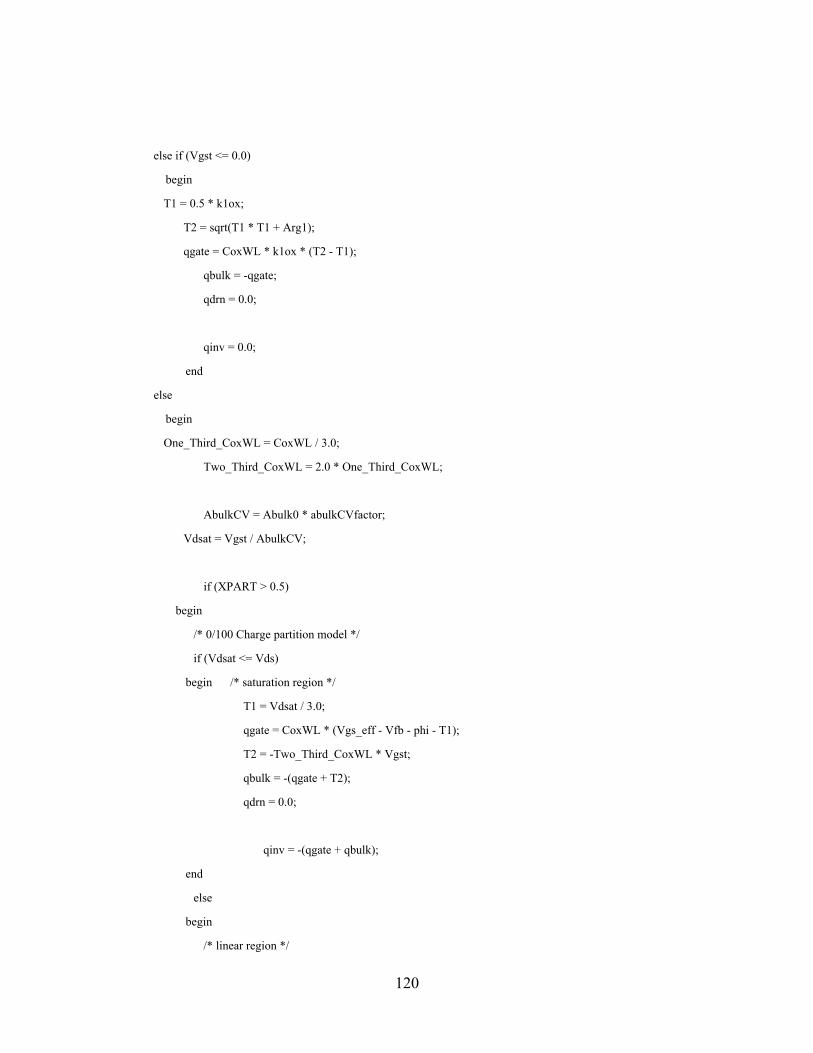
120
else if (Vgst <= 0.0)
begin
T1 = 0.5 * k1ox;
T2 = sqrt(T1 * T1 + Arg1);
qgate = CoxWL * k1ox * (T2 - T1);
qbulk = -qgate;
qdrn = 0.0;
qinv = 0.0;
end
else
begin
One_Third_CoxWL = CoxWL / 3.0;
Two_Third_CoxWL = 2.0 * One_Third_CoxWL;
AbulkCV = Abulk0 * abulkCVfactor;
Vdsat = Vgst / AbulkCV;
if (XPART > 0.5)
begin
/* 0/100 Charge partition model */
if (Vdsat <= Vds)
begin /* saturation region */
T1 = Vdsat / 3.0;
qgate = CoxWL * (Vgs_eff - Vfb - phi - T1);
T2 = -Two_Third_CoxWL * Vgst;
qbulk = -(qgate + T2);
qdrn = 0.0;
qinv = -(qgate + qbulk);
end
else
begin
/* linear region */
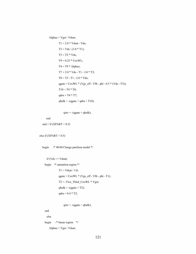
121
Alphaz = Vgst / Vdsat;
T1 = 2.0 * Vdsat - Vds;
T2 = Vds / (3.0 * T1);
T3 = T2 * Vds;
T9 = 0.25 * CoxWL;
T4 = T9 * Alphaz;
T7 = 2.0 * Vds - T1 - 3.0 * T3;
T8 = T3 - T1 - 2.0 * Vds;
qgate = CoxWL * (Vgs_eff - Vfb - phi - 0.5 * (Vds - T3));
T10 = T4 * T8;
qdrn = T4 * T7;
qbulk = -(qgate + qdrn + T10);
qinv = -(qgate + qbulk);
end
end // if (XPART > 0.5)
else if (XPART < 0.5)
begin /* 40/60 Charge partition model */
if (Vds >= Vdsat)
begin /* saturation region */
T1 = Vdsat / 3.0;
qgate = CoxWL * (Vgs_eff - Vfb - phi - T1);
T2 = -Two_Third_CoxWL * Vgst;
qbulk = -(qgate + T2);
qdrn = 0.4 * T2;
qinv = -(qgate + qbulk);
end
else
begin /* linear region */
Alphaz = Vgst / Vdsat;
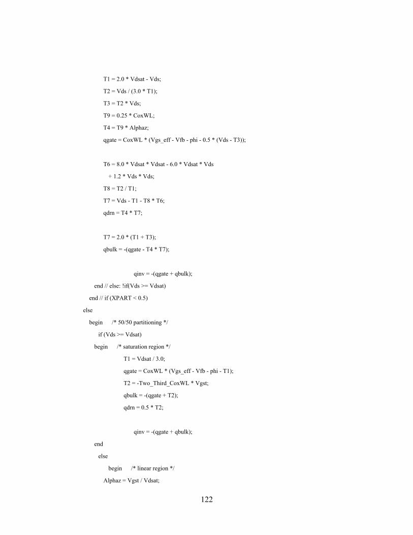
122
T1 = 2.0 * Vdsat - Vds;
T2 = Vds / (3.0 * T1);
T3 = T2 * Vds;
T9 = 0.25 * CoxWL;
T4 = T9 * Alphaz;
qgate = CoxWL * (Vgs_eff - Vfb - phi - 0.5 * (Vds - T3));
T6 = 8.0 * Vdsat * Vdsat - 6.0 * Vdsat * Vds
+ 1.2 * Vds * Vds;
T8 = T2 / T1;
T7 = Vds - T1 - T8 * T6;
qdrn = T4 * T7;
T7 = 2.0 * (T1 + T3);
qbulk = -(qgate - T4 * T7);
qinv = -(qgate + qbulk);
end // else: !if(Vds >= Vdsat)
end // if (XPART < 0.5)
else
begin /* 50/50 partitioning */
if (Vds >= Vdsat)
begin /* saturation region */
T1 = Vdsat / 3.0;
qgate = CoxWL * (Vgs_eff - Vfb - phi - T1);
T2 = -Two_Third_CoxWL * Vgst;
qbulk = -(qgate + T2);
qdrn = 0.5 * T2;
qinv = -(qgate + qbulk);
end
else
begin /* linear region */
Alphaz = Vgst / Vdsat;
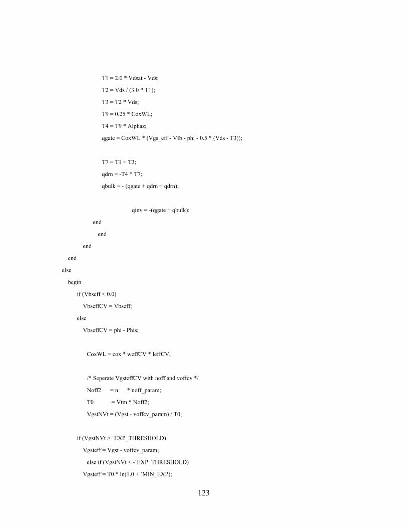
123
T1 = 2.0 * Vdsat - Vds;
T2 = Vds / (3.0 * T1);
T3 = T2 * Vds;
T9 = 0.25 * CoxWL;
T4 = T9 * Alphaz;
qgate = CoxWL * (Vgs_eff - Vfb - phi - 0.5 * (Vds - T3));
T7 = T1 + T3;
qdrn = -T4 * T7;
qbulk = - (qgate + qdrn + qdrn);
qinv = -(qgate + qbulk);
end
end
end
end
else
begin
if (Vbseff < 0.0)
VbseffCV = Vbseff;
else
VbseffCV = phi - Phis;
CoxWL = cox * weffCV * leffCV;
/* Seperate VgsteffCV with noff and voffcv */
Noff2 = n * noff_param;
T0 = Vtm * Noff2;
VgstNVt = (Vgst - voffcv_param) / T0;
if (VgstNVt > `EXP_THRESHOLD)
Vgsteff = Vgst - voffcv_param;
else if (VgstNVt < -`EXP_THRESHOLD)
Vgsteff = T0 * ln(1.0 + `MIN_EXP);
124
else
begin
ExpVgst = exp(VgstNVt);
Vgsteff = T0 * ln(1.0 + ExpVgst);
end /* End of VgsteffCV - Weidong 5/1998 */
if (CAPMOD == 1)
begin
if (VERSION < 3.2)
Vfb = Vth - phi - k1ox * sqrtPhis;
else
Vfb = vfbzb;
Arg1 = Vgs_eff - VbseffCV - Vfb - Vgsteff;
if (Arg1 <= 0.0)
qgate = CoxWL * Arg1;
else
begin
T0 = 0.5 * k1ox;
T1 = sqrt(T0 * T0 + Arg1);
qgate = CoxWL * k1ox * (T1 - T0);
end
qbulk = -qgate;
One_Third_CoxWL = CoxWL / 3.0;
Two_Third_CoxWL = 2.0 * One_Third_CoxWL;
AbulkCV = Abulk0 * abulkCVfactor;
VdsatCV = Vgsteff / AbulkCV;
if (VdsatCV < Vds)
begin
125
T0 = Vgsteff - VdsatCV / 3.0;
qgate = qgate + CoxWL * T0;
T0 = VdsatCV - Vgsteff;
qbulk = qbulk + One_Third_CoxWL * T0;
if (XPART > 0.5)
T0 = -Two_Third_CoxWL;
else if (XPART < 0.5)
T0 = -0.4 * CoxWL;
else
T0 = -One_Third_CoxWL;
qsrc = T0 * Vgsteff;
end
else
begin
T0 = AbulkCV * Vds;
T1 = 12.0 * (Vgsteff - 0.5 * T0 + 1.0e-20);
T2 = Vds / T1;
T3 = T0 * T2;
qgate = qgate + CoxWL * (Vgsteff - 0.5 * Vds + T3);
qbulk = qbulk + CoxWL * (1.0 - AbulkCV) * (0.5 * Vds - T3);
if (XPART > 0.5)
begin /* 0/100 Charge petition model */
qsrc = -CoxWL * (0.5 * Vgsteff + 0.25 * T0 - T0 * T0 / (T1 + T1));
end
else if (XPART < 0.5)
begin /* 40/60 Charge petition model */
T2 = 0.5 * CoxWL / (T1 / 12.0 * T1 / 12.0);
T3 = Vgsteff * (2.0 * T0 * T0 / 3.0 + Vgsteff * (Vgsteff - 4.0 * T0 / 3.0))
- 2.0 * T0 * T0 * T0 / 15.0;
126
qsrc = -T2 * T3;
end
else
begin /* 50/50 Charge petition model */
qsrc = -0.5 * (qgate + qbulk);
end
end
qdrn = -(qgate + qbulk + qsrc);
qinv = -(qgate + qbulk);
end // if (CAPMOD == 1)
else if (CAPMOD == 2)
begin
if (VERSION < 3.2)
Vfb = Vth - phi - k1ox * sqrtPhis;
else
Vfb = vfbzb;
V3 = Vfb - Vgs_eff + VbseffCV - `DELTA_3;
if (Vfb <= 0.0)
begin
T0 = sqrt(V3 * V3 - 4.0 * `DELTA_3 * Vfb);
T2 = -`DELTA_3 / T0;
end
else
begin
T0 = sqrt(V3 * V3 + 4.0 * `DELTA_3 * Vfb);
T2 = `DELTA_3 / T0;
end
T1 = 0.5 * (1.0 + V3 / T0);
Vfbeff = Vfb - 0.5 * (V3 + T0);
Qac0 = CoxWL * (Vfbeff - Vfb);
127
T0 = 0.5 * k1ox;
T3 = Vgs_eff - Vfbeff - VbseffCV - Vgsteff;
if (k1ox == 0.0)
begin
T1 = 0.0;
T2 = 0.0;
end
else if (T3 < 0.0)
begin
T1 = T0 + T3 / k1ox;
T2 = CoxWL;
end
else
begin
T1 = sqrt(T0 * T0 + T3);
T2 = CoxWL * T0 / T1;
end
Qsub0 = CoxWL * k1ox * (T1 - T0);
AbulkCV = Abulk0 * abulkCVfactor;
VdsatCV = Vgsteff / AbulkCV;
V4 = VdsatCV - Vds - `DELTA_4;
T0 = sqrt(V4 * V4 + 4.0 * `DELTA_4 * VdsatCV);
VdseffCV = VdsatCV - 0.5 * (V4 + T0);
/* Added to eliminate non-zero VdseffCV at Vds=0.0 */
if ((Vds == 0.0) && (VERSION == 3.24))
VdseffCV = 0.0;
T0 = AbulkCV * VdseffCV;
128
T1 = 12.0 * (Vgsteff - 0.5 * T0 + 1e-20);
T2 = VdseffCV / T1;
T3 = T0 * T2;
T4 = (1.0 - 12.0 * T2 * T2 * AbulkCV);
T5 = (6.0 * T0 * (4.0 * Vgsteff - T0) / (T1 * T1) - 0.5);
T6 = 12.0 * T2 * T2 * Vgsteff;
qinoi = -CoxWL * (Vgsteff - 0.5 * T0 + AbulkCV * T3);
qgate = CoxWL * (Vgsteff - 0.5 * VdseffCV + T3);
T7 = 1.0 - AbulkCV;
qbulk = CoxWL * T7 * (0.5 * VdseffCV - T3);
if (XPART > 0.5)
begin /* 0/100 Charge petition model */
qsrc = -CoxWL * (0.5 * Vgsteff + 0.25 * T0 - T0 * T0 / (T1 + T1));
end
else if (XPART < 0.5)
begin /* 40/60 Charge petition model */
T2 = 0.5 * CoxWL / (T1 / 12.0 * T1 / 12.0);
T3 = Vgsteff * (2.0 * T0 * T0 / 3.0 + Vgsteff * (Vgsteff - 4.0 * T0 / 3.0))
- 2.0 * T0 * T0 * T0 / 15.0;
qsrc = -T2 * T3;
end
else
begin /* 50/50 Charge petition model */
qsrc = -0.5 * (qgate + qbulk);
end
qgate = qgate + Qac0 + Qsub0;
qbulk = qbulk - (Qac0 + Qsub0);
qdrn = -(qgate + qbulk + qsrc);
129
qinv = qinoi;
end
/* New Charge-Thickness capMod (CTM) begins - Weidong 7/1997 */
else if (CAPMOD == 3)
begin
V3 = vfbzb - Vgs_eff + VbseffCV - `DELTA_3;
if (vfbzb <= 0.0)
begin
T0 = sqrt(V3 * V3 - 4.0 * `DELTA_3 * vfbzb);
T2 = -`DELTA_3 / T0;
end
else
begin
T0 = sqrt(V3 * V3 + 4.0 * `DELTA_3 * vfbzb);
T2 = `DELTA_3 / T0;
end
T1 = 0.5 * (1.0 + V3 / T0);
Vfbeff = vfbzb - 0.5 * (V3 + T0);
Cox = cox;
Tox = 1.0e8 * tox;
T0 = (Vgs_eff - VbseffCV - vfbzb) / Tox;
tmp = T0 * acde;
if ((-`EXP_THRESHOLD < tmp) && (tmp < `EXP_THRESHOLD))
Tcen = ldeb * exp(tmp);
else if (tmp <= -`EXP_THRESHOLD)
Tcen = ldeb * `MIN_EXP;
else
Tcen = ldeb * `MAX_EXP;
130
LINK = 1.0e-3 * tox;
V3 = ldeb - Tcen - LINK;
V4 = sqrt(V3 * V3 + 4.0 * LINK * ldeb);
Tcen = ldeb - 0.5 * (V3 + V4);
T1 = 0.5 * (1.0 + V3 / V4);
Ccen = `EPSSI / Tcen;
T2 = Cox / (Cox + Ccen);
Coxeff = T2 * Ccen;
T3 = -Ccen / Tcen;
CoxWLcen = CoxWL * Coxeff / Cox;
Qac0 = CoxWLcen * (Vfbeff - vfbzb);
T0 = 0.5 * k1ox;
T3 = Vgs_eff - Vfbeff - VbseffCV - Vgsteff;
if (k1ox == 0.0)
begin
T1 = 0.0;
T2 = 0.0;
end
else if (T3 < 0.0)
begin
T1 = T0 + T3 / k1ox;
T2 = CoxWLcen;
end
else
begin
T1 = sqrt(T0 * T0 + T3);
T2 = CoxWLcen * T0 / T1;
end
Qsub0 = CoxWLcen * k1ox * (T1 - T0);
131
/* Gate-bias dependent delta Phis begins */
if (k1ox <= 0.0)
begin
Denomi = 0.25 * moin * Vtm;
T0 = 0.5 * sqrtPhi;
end
else
begin
Denomi = moin * Vtm * k1ox * k1ox;
T0 = k1ox * sqrtPhi;
end
T1 = 2.0 * T0 + Vgsteff;
DeltaPhi = Vtm * ln(1.0 + T1 * Vgsteff / Denomi);
/* End of delta Phis */
T3 = 4.0 * (Vth - vfbzb - phi);
Tox2 = Tox + Tox;
if (T3 >= 0.0)
T0 = (Vgsteff + T3) / Tox2;
else
T0 = (Vgsteff + 1.0e-20) / Tox2;
tmp = exp(0.7 * ln(T0));
T1 = 1.0 + tmp;
T2 = 0.7 * tmp / (T0 * Tox2);
Tcen = 1.9e-9 / T1;
Ccen = `EPSSI / Tcen;
T0 = Cox / (Cox + Ccen);
Coxeff = T0 * Ccen;
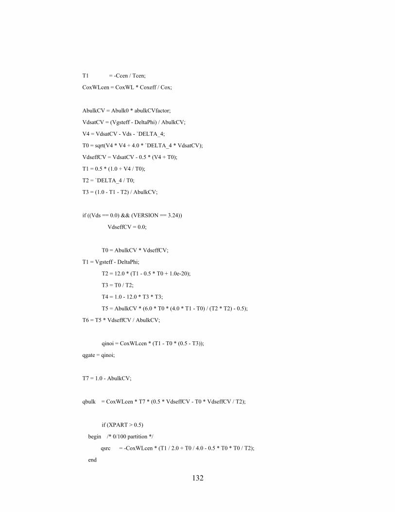
132
T1 = -Ccen / Tcen;
CoxWLcen = CoxWL * Coxeff / Cox;
AbulkCV = Abulk0 * abulkCVfactor;
VdsatCV = (Vgsteff - DeltaPhi) / AbulkCV;
V4 = VdsatCV - Vds - `DELTA_4;
T0 = sqrt(V4 * V4 + 4.0 * `DELTA_4 * VdsatCV);
VdseffCV = VdsatCV - 0.5 * (V4 + T0);
T1 = 0.5 * (1.0 + V4 / T0);
T2 = `DELTA_4 / T0;
T3 = (1.0 - T1 - T2) / AbulkCV;
if ((Vds == 0.0) && (VERSION == 3.24))
VdseffCV = 0.0;
T0 = AbulkCV * VdseffCV;
T1 = Vgsteff - DeltaPhi;
T2 = 12.0 * (T1 - 0.5 * T0 + 1.0e-20);
T3 = T0 / T2;
T4 = 1.0 - 12.0 * T3 * T3;
T5 = AbulkCV * (6.0 * T0 * (4.0 * T1 - T0) / (T2 * T2) - 0.5);
T6 = T5 * VdseffCV / AbulkCV;
qinoi = CoxWLcen * (T1 - T0 * (0.5 - T3));
qgate = qinoi;
T7 = 1.0 - AbulkCV;
qbulk = CoxWLcen * T7 * (0.5 * VdseffCV - T0 * VdseffCV / T2);
if (XPART > 0.5)
begin /* 0/100 partition */
qsrc = -CoxWLcen * (T1 / 2.0 + T0 / 4.0 - 0.5 * T0 * T0 / T2);
end
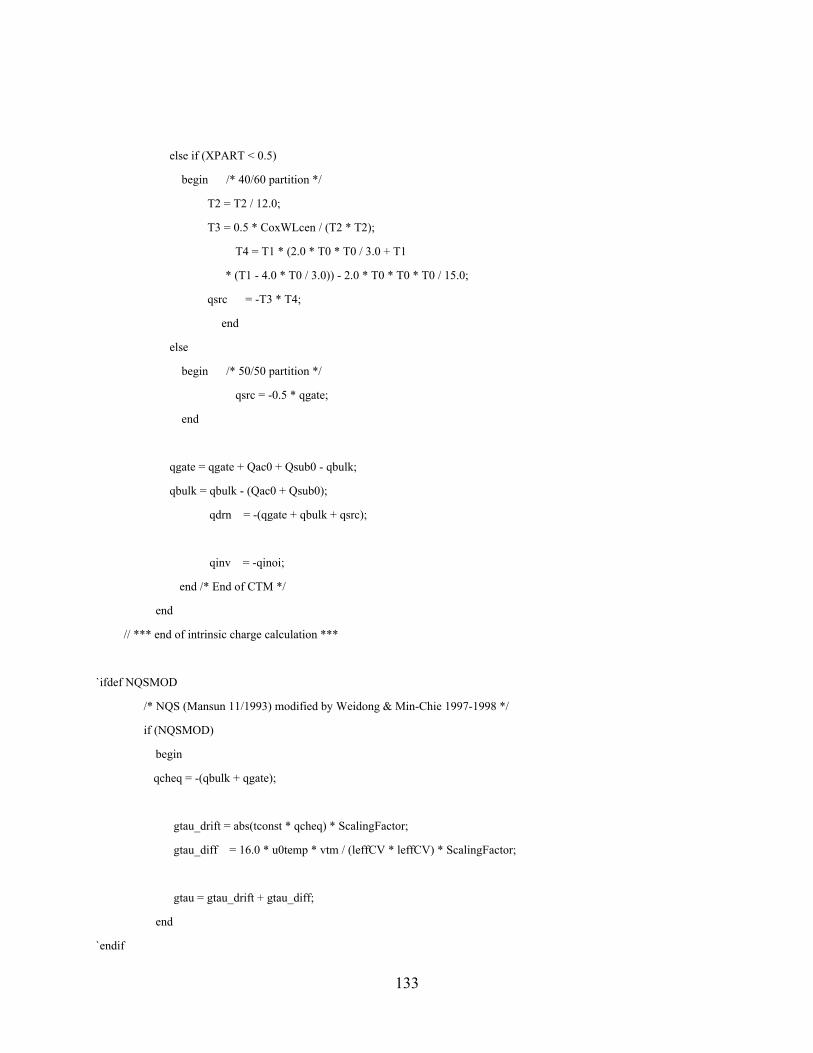
133
else if (XPART < 0.5)
begin /* 40/60 partition */
T2 = T2 / 12.0;
T3 = 0.5 * CoxWLcen / (T2 * T2);
T4 = T1 * (2.0 * T0 * T0 / 3.0 + T1
* (T1 - 4.0 * T0 / 3.0)) - 2.0 * T0 * T0 * T0 / 15.0;
qsrc = -T3 * T4;
end
else
begin /* 50/50 partition */
qsrc = -0.5 * qgate;
end
qgate = qgate + Qac0 + Qsub0 - qbulk;
qbulk = qbulk - (Qac0 + Qsub0);
qdrn = -(qgate + qbulk + qsrc);
qinv = -qinoi;
end /* End of CTM */
end
// *** end of intrinsic charge calculation ***
`ifdef NQSMOD
/* NQS (Mansun 11/1993) modified by Weidong & Min-Chie 1997-1998 */
if (NQSMOD)
begin
qcheq = -(qbulk + qgate);
gtau_drift = abs(tconst * qcheq) * ScalingFactor;
gtau_diff = 16.0 * u0temp * vtm / (leffCV * leffCV) * ScalingFactor;
gtau = gtau_drift + gtau_diff;
end
`endif
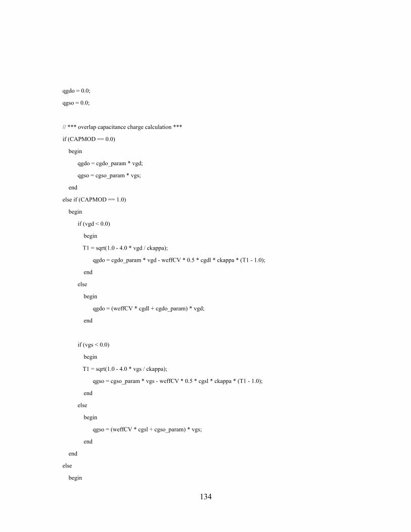
134
qgdo = 0.0;
qgso = 0.0;
// *** overlap capacitance charge calculation ***
if (CAPMOD == 0.0)
begin
qgdo = cgdo_param * vgd;
qgso = cgso_param * vgs;
end
else if (CAPMOD == 1.0)
begin
if (vgd < 0.0)
begin
T1 = sqrt(1.0 - 4.0 * vgd / ckappa);
qgdo = cgdo_param * vgd - weffCV * 0.5 * cgdl * ckappa * (T1 - 1.0);
end
else
begin
qgdo = (weffCV * cgdl + cgdo_param) * vgd;
end
if (vgs < 0.0)
begin
T1 = sqrt(1.0 - 4.0 * vgs / ckappa);
qgso = cgso_param * vgs - weffCV * 0.5 * cgsl * ckappa * (T1 - 1.0);
end
else
begin
qgso = (weffCV * cgsl + cgso_param) * vgs;
end
end
else
begin
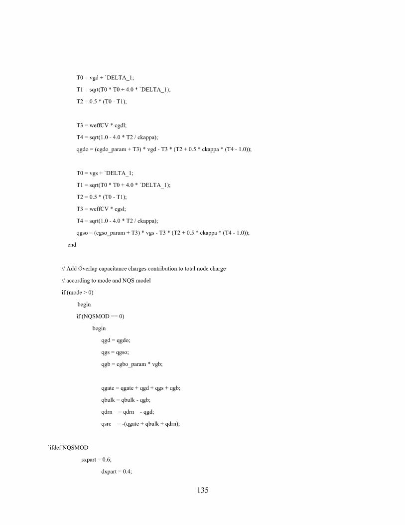
135
T0 = vgd + `DELTA_1;
T1 = sqrt(T0 * T0 + 4.0 * `DELTA_1);
T2 = 0.5 * (T0 - T1);
T3 = weffCV * cgdl;
T4 = sqrt(1.0 - 4.0 * T2 / ckappa);
qgdo = (cgdo_param + T3) * vgd - T3 * (T2 + 0.5 * ckappa * (T4 - 1.0));
T0 = vgs + `DELTA_1;
T1 = sqrt(T0 * T0 + 4.0 * `DELTA_1);
T2 = 0.5 * (T0 - T1);
T3 = weffCV * cgsl;
T4 = sqrt(1.0 - 4.0 * T2 / ckappa);
qgso = (cgso_param + T3) * vgs - T3 * (T2 + 0.5 * ckappa * (T4 - 1.0));
end
// Add Overlap capacitance charges contribution to total node charge
// according to mode and NQS model
if (mode > 0)
begin
if (NQSMOD == 0)
begin
qgd = qgdo;
qgs = qgso;
qgb = cgbo_param * vgb;
qgate = qgate + qgd + qgs + qgb;
qbulk = qbulk - qgb;
qdrn = qdrn - qgd;
qsrc = -(qgate + qbulk + qdrn);
`ifdef NQSMOD
sxpart = 0.6;
dxpart = 0.4;
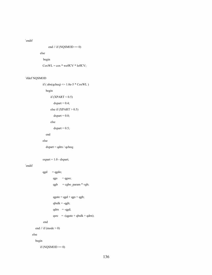
136
`endif
end // if (NQSMOD == 0)
else
begin
CoxWL = cox * weffCV * leffCV;
`ifdef NQSMOD
if ( abs(qcheq) <= 1.0e-5 * CoxWL )
begin
if (XPART < 0.5)
dxpart = 0.4;
else if (XPART > 0.5)
dxpart = 0.0;
else
dxpart = 0.5;
end
else
dxpart = qdrn / qcheq;
sxpart = 1.0 - dxpart;
`endif
qgd = qgdo;
qgs = qgso;
qgb = cgbo_param * vgb;
qgate = qgd + qgs + qgb;
qbulk = -qgb;
qdrn = -qgd;
qsrc = -(qgate + qbulk + qdrn);
end
end // if (mode > 0)
else
begin
if (NQSMOD == 0)
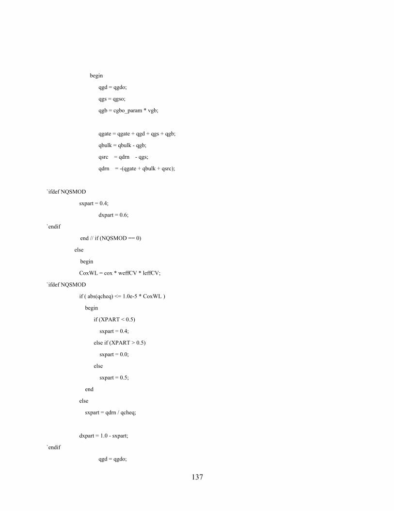
137
begin
qgd = qgdo;
qgs = qgso;
qgb = cgbo_param * vgb;
qgate = qgate + qgd + qgs + qgb;
qbulk = qbulk - qgb;
qsrc = qdrn - qgs;
qdrn = -(qgate + qbulk + qsrc);
`ifdef NQSMOD
sxpart = 0.4;
dxpart = 0.6;
`endif
end // if (NQSMOD == 0)
else
begin
CoxWL = cox * weffCV * leffCV;
`ifdef NQSMOD
if ( abs(qcheq) <= 1.0e-5 * CoxWL )
begin
if (XPART < 0.5)
sxpart = 0.4;
else if (XPART > 0.5)
sxpart = 0.0;
else
sxpart = 0.5;
end
else
sxpart = qdrn / qcheq;
dxpart = 1.0 - sxpart;
`endif
qgd = qgdo;
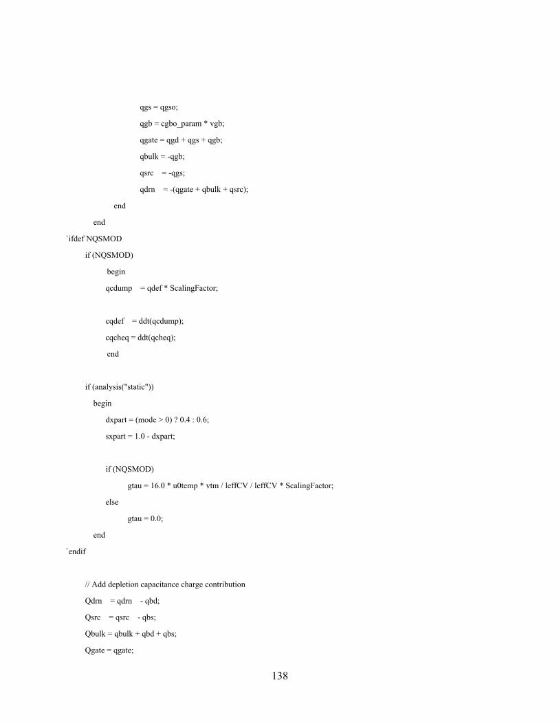
138
qgs = qgso;
qgb = cgbo_param * vgb;
qgate = qgd + qgs + qgb;
qbulk = -qgb;
qsrc = -qgs;
qdrn = -(qgate + qbulk + qsrc);
end
end
`ifdef NQSMOD
if (NQSMOD)
begin
qcdump = qdef * ScalingFactor;
cqdef = ddt(qcdump);
cqcheq = ddt(qcheq);
end
if (analysis("static"))
begin
dxpart = (mode > 0) ? 0.4 : 0.6;
sxpart = 1.0 - dxpart;
if (NQSMOD)
gtau = 16.0 * u0temp * vtm / leffCV / leffCV * ScalingFactor;
else
gtau = 0.0;
end
`endif
// Add depletion capacitance charge contribution
Qdrn = qdrn - qbd;
Qsrc = qsrc - qbs;
Qbulk = qbulk + qbd + qbs;
Qgate = qgate;
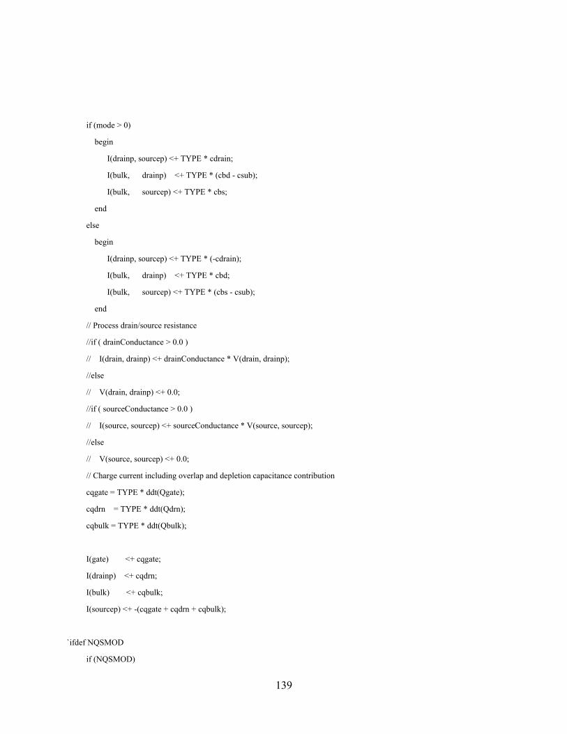
139
if (mode > 0)
begin
I(drainp, sourcep) <+ TYPE * cdrain;
I(bulk, drainp) <+ TYPE * (cbd - csub);
I(bulk, sourcep) <+ TYPE * cbs;
end
else
begin
I(drainp, sourcep) <+ TYPE * (-cdrain);
I(bulk, drainp) <+ TYPE * cbd;
I(bulk, sourcep) <+ TYPE * (cbs - csub);
end
// Process drain/source resistance
//if ( drainConductance > 0.0 )
// I(drain, drainp) <+ drainConductance * V(drain, drainp);
//else
// V(drain, drainp) <+ 0.0;
//if ( sourceConductance > 0.0 )
// I(source, sourcep) <+ sourceConductance * V(source, sourcep);
//else
// V(source, sourcep) <+ 0.0;
// Charge current including overlap and depletion capacitance contribution
cqgate = TYPE * ddt(Qgate);
cqdrn = TYPE * ddt(Qdrn);
cqbulk = TYPE * ddt(Qbulk);
I(gate) <+ cqgate;
I(drainp) <+ cqdrn;
I(bulk) <+ cqbulk;
I(sourcep) <+ -(cqgate + cqdrn + cqbulk);
`ifdef NQSMOD
if (NQSMOD)
140
begin
I(gate) <+ TYPE * (-1) * qdef * gtau;
I(drainp) <+ TYPE * dxpart * qdef * gtau;
I(sourcep) <+ TYPE * sxpart * qdef * gtau;
I(q) <+ -TYPE * ( cqdef - cqcheq );
I(q) <+ -V(q) * gtau;
end
else
begin
I(q) <+ GMIN * qdef;
end
`endif
end // analog begin
endmodule
141
REFERENCES [1] Arnold Reismann, “Device, Circuit, and Technology Scaling to Micron and Submicron
Dimensions” Proc. IEEE, vol. 71, no. 5, pp. 550-565, May 1983. [2] Cheng T. Wang, “Hot Carrier Design Considerations for MOS Devices and Circuits” Van
Nostrand Reinhold, 1990. [3] S. M. Sze, “Physics of Semiconductor Devices” Wiley Eastern Limited, New Delhi, 1981. [4] Chenming Hu, “Lucky Electron Model of Channel Hot Electron Emission” in Proc. IEDM,
1979. [5] Y. Nissan-Cohen, J. Shappir, and D. Frohman-Bentchkowsky, “Trap Generation and
Occupation Dynamics in SiO2 under Charge Injection Stress” J. Appl. Phys., vol. 60, no. 6, pp. 2024-2035, Sept. 1986.
[6] Brian Doyle, Marc Bourcerie, Jean-Claude Marchetaux, and Alain Boudou, “Interface State
Creation and Charge Trapping in the Medium-to-High Gate Voltage Range Vd >=Vg >= Vd) During Hot-Carrier Stressing of nMOS Transistors” IEEE Transactions on Electron Devices, vol. 37, no. 3, pp. 744-754, March 1990.
[7] L. Lipkin, A. Reisman, and C. K. Williams, “Hole Trapping Phenomena in the gate Insulator
of As-Fabricated Insulated Gate Field Effect Transistors” J. Appl. Phys., vol. 68, no. 9, pp. 4620-4633, Nov. 1990.
[8] S. J. Wang, J. M. Sung, and S. A. Lyon, “Relationship Between Hole Trapping and Interface
State Generation in Metal-Oxide-Silicon Structures” Applied Physics Letters, vol. 52, no. 17, pp. 1431-1433, April 1988.
[9] S. Lai, “Two-Carrier Nature of Interface-State Generation in Hole Trapping and Radiation
Damage” Appl. Phys. Lett., vol. 39, pp. 58, 1981.
142
[10] Y. Roh, “Interface Traps Induced by Hole Trapping in Metal-Oxide Semiconductor Devices” J. Non-Cryst. Sol., vol. 187, pp. 165-169, 1995.
[11] Tah. H. Ning, Peter W. Cook, Robert H. Dennard, Carlton M. Osburn, Stanley E. Schuster,
and Hwa-Nien Yu, “1μm MOSFET VLSI Technology : Part IV Hot-Electron Design Constraints” IEEE Transactions on Electron Devices, vol. ED-26, no. 4, pp. 346-352, Apr. 1979.
[12] Eiji Takeda, Hitoshi Kume, Toru Toyabe, and Shojiro Asai, “Submicrometer MOSFET
Structure for Minimizing Hot-Carrier Generation” IEEE Transactions on Electron Devices, vol. ED-29, no. 4, pp. 611-618, Apr. 1982.
[13] T. Poorter and P. Zoestbergen, “Hot-Carrier E_ects in MOS Transistors” Proc. IEDM, pp.
100-103, 1984. [14] T. H. Ning and H. N. Yu, “Optically Induced Injection of Hot Electrons into SiO2” Journal of
Applied Physics, vol. 45, no. 12, pp. 5373-5378, December 1974. [15] R. J. Milanowski, M. P. Pagey, A. I. Matta, L. W. Massengill, B. L. Bhuva, and S. E. Kerns,
“Combined E_ect of X-Irradiation and Forming Gas Anneal on the Hot-Carrier Response of MOS Oxides” IEEE Trans. Nucl. Sci., vol. 40, pp. 1360-1366, Dec. 1993.
[16] P. J. McWhorter and P. S. Winokur, “Simple Technique for Separating the Effects of Interface
Traps and Trapped-Oxide Charge in Metal-Oxide-Semiconductor Transistors” Appl. Phys. Lett., vol. 48, no. 2, pp. 133-134, Jan. 1986.
[17] H. E. Maes, “Hot-Carrier Degradation in Submicron MOSFETs, Ph.D. thesis [18] P. K. Ko, J. H. Huang, Z. H. Liu, and C. Hu, “BSIM3 for Analog and Digital Circuit
Simulation” IEEE Symp. on VLSI Tech. CAD, pp. 400-429, January 1993. [19] C. Hu, S. C. Tam, F. C. Hsu, P. K. Ko, T. Y. Chan, and K.W. Terrill, “Hot-electron induced
MOSFET degradation-modle, monitor and improvement” IEEE Transactions on Electron Devices, vol. ED-32, pp. 297-302, 1985.
143
[20] J.-P. Colinge,, “Hot-electron effects in silicon-insulator N-channel MOSFET’s,” IEEE
Transactions on Electron Devices, vol. ED-34, pp.2173-2177, 1987. [21] E. Takeda and N. Suzuki, “An empirical model for device degradation due to hot-carrier
injection,” IEEE Electron Devices Letter,vol. EDL-4, pp. 111-113, 1983. [22] T. Tsuchiya, Y. Okazaki, M. Miyake, and T. Kobayashi, “New hot-carrier degradation mode
and lifetime prediction method in quarter-micrometer pMOSFET,” IEEE Transaction Electron Devices, pp. 404-408, Feb. 1992.
[23] K.Takeuchi, T. Yamanoto, A. Tanabe, T. Matsuki, T. Kunio, M. Fukuma, K. Nakajima, H.
Aizaki, H. Miyanoto, and E. Ikawa, “0.15 μm CMOS with high reliability and performance,” in IEDM Tech. Dig., 1993.
[24] J. J. Liou, A. Ortiz-Conde, and F. Garcia-Sanchez, “Analysis and Design of MOSFETs:
Modeling, Simulation, and Parameter Extraction” Boston, MA: Kluwer, 1998. [25] E. Takeda and N. Suzuki, “An empirical model for device degradation due to hot carrier
injection” IEEE Electron. Device Lett., vol. EDL-4, pp. 111–113, 1983. [26] V. H. Chan and J. E. Chung, “Two-stage hot carrier degradation and its impact on
submicrometer LDD NMOSFET lifetime prediction” IEEE Trans. Electron. Devices, vol. 42, pp. 957–962, 1995.
[27] B. Marchand, G. Ghibaudo, F. Balestra, G. Guegan, and S. Deleonibus, “A new hot carrier
degradation law for MOSFET lifetime prediction” Microelectron. Reliab., pp. 1103–1107, 1998.
[28] B. Szelag, S. Kubicek, K. De Meyer, and F. Balestra, “Time-dependent degradation law for
reliable lifetime prediction in sub-0.25 um bulk silicon N-MOSFETs” Electron. Lett., vol. 35, no. 35, pp. 1385–1386, 1999.
144
[29] S.H. Renn, J.L. Pelloie, and F. Balestra, “Hot-carrier effects and reliable lifetime prediction in deep submicron N- and P-channel SOI MOSFET’s” IEEE Trans. Electron. Devices, vol. 45, pp. 2335–2342, Nov. 1998.
[30] C. Hu, S. C. Tam, F. C. Hsu, P. K. Ko, T. Y. Chan, and K. W. Terrill, “Hot-electron induced
MOSFET degradation-model, monitor and improvement” IEEE Trans. Electron Devices, Vol. ED-32, pp. 375-385, 1985.
[31] R. Bellens, P. Heremans, G. Groeseneken, and H. Maes, “On the channel-length dependence
of the hot-carrier degradation of n-channel MOSFET’s” IEEE Electron Device Lett., Vol. 10, No. 12, pp. 553-555, 1989.
[32] E. Takeda and N. Suzuki, “An empirical model for device degradation due to hot-carrier
injection” IEEE Electron Device Lett., vol. EDL-4, pp. pp. 111-113, 1983. [33] Z. Chi, J. J. Liou, and Y. Yue, “A new extrapolation method for long-term degradation
prediction of deep-submicron MOSFETs” IEEE Electron Devices, accepted for publication, Dec. 2002.
[34] J. J. Liou, A. Ortiz-Conde, and F. Garcia-Sanchez, Analysis and Design of MOSFETs:
Modeling, Simulation, and Parameter Extraction, Kluwer Academic Publishers, 1998. [35] J. Lee, G. Bosman, K. R. Green, and D. Ladwig, “Model and analysis of gate leakage current
in ultrathin nitrided oxide MOSFETs,” IEEE Trans. Electron Devices, vol.49, pp.1232-1241, 2002.
[36] A. Ghetti, E. Sangiorgi, J. Bude, T. W. Sorsch and G. Weber, “Tunneling into interface States
as reliability monitor for ultrathin oxides,” IEEE Trans. Electron Devices, vol.47, pp.2358-2365, 2000.
[37] H. Momose, M. Ono, T. Yoshitomi, T. Ohguro, S. Nakamura, H. Iwai and M. Saito, 1.5 nm
direct-tunnelling gate oxide Si MOSFET's. IEEE Trans Electron Device, vol 43, pp. 1233–1241, 1996.
145
[38] H. Hu, J. B. Jacobs, J. E. Chung, and D. A. Antoniadis, “The correlation between gate current and substrate current in 0.1 μm NMOFET’s”, IEEE Electron Device Lett., vol. 15, 1994.
[39] P. Heremans, G. Groeseneken, and H. E. Maes, “Consistent model for the hot-carrier
degradation in n-channel and p-channel MOSFETs”, IEEE Trans. Electron Devices, vol. 35, pp. 2194-2209, 1988.
[40] H. Wong and Y. C. Cheng, "Modeling of Hot Electron Induced MOS Characteristic
Degradations," Solid State Electron., vol.36, pp.1469-1475, 1993. [41] D. J. DiMaria and J. H. Stathis, “Trapping and trap creation studies on nitrided and reoxidized
silicon dioxide films on silicon,” J. Appl. Phys., vol.70, pp.1500-1509, 1991 [42] H. Wong and Y. C. Cheng, "Generation of interface states at the silicon/oxide interface due to
hot electron injection," J. Appl. Phys., vol.74, pp.7364-7368, 1993. [43] Z. Cui, J. J. Liou, and Y. Yue, “A new extrapolation method for long-term degradation
prediction of deep-submicron MOSFETs,” IEEE Trans. Electron Devices, vol. 50, pp. 1398-1401, 2003.
[44] H. Wong, "A Physically Based Drain Avalanche Breakdown Model for MOSFET’s," IEEE
Trans. Electron Devices, vol.42, pp.2197-2202, 1995. [45] H. Wong and M. C. Poon, “Approximation of the Length of Velocity Saturation Region in
MOSFET’s”, IEEE Trans. Electron Devices, vol.44, pp.2033-2035, 1997. [46] P. K. Ko, “Approaches to Scaling,” in Advanced MOS Device Physics, N. G. Einspruch and G.
Gildenblat, Eds. New York: Academic, 1989. [47] B. W. Min, O. Zia, M. Celik, R. Widenhofer, L. Kang, S. Song, and S. Gonzales, “Hot Carrier
Enhanced Gate Current and Its Impact on Short Channel nMOSFET Reliability with Ultra-thin Gate Oxides”, IEEE IEDM Technical Dig., pp. 873-875, 2001
146
[48] F. Mu, M. Xu, C. Tan, and X. Duan, “A new lifetime prediction method for hot-carrier degradation in n-MOSFETs with ultrathin gate oxides under Vg=Vd”, Microelectron. Reliab., vol. 41, pp. 1909-1913, 2001
[49] C. Hu, S. C. Tam, F. C. Hsu, P. K. Ko, T. H. Chan, and K. W. Terrill, “Hot-electron-induced
MOSFET degradation model monitor and improvement,” IEEE Trans. Electron Devices, vol.32, pp.375-385, 1985.
[50] H. Wong, “Modeling of the Parasitic Transistor-Induced Drain Breakdown in MOSFET’s”,
IEEE Trans. Electron Devices, vol.43, pp.2190-2196, 1996. [51] V. A. Gritsenko, H. Wong, J. B. Xu, R. M. Kwok, I. P. Petrenko, B. A. Zaitsev, Yu.N.
Morokov, and Yu. N. Novikov, "Excess silicon at the silicon nitride/thermal oxide interface in oxide-nitride-oxide structures," J. Appl. Phys., vol.86, pp.3234-3240, Sept. 1999.
[52] H. Wong and V. A. Gritsenko, “Defects in silicon oxynitride gate dielectric films,”
Microelectron. Reliab., vol. 42, pp. 597-605, Apr. & May, 2002. [53] H. Wong, M. C. Poon, C. W. Kok, P. J. Chan, V. A. Gritsenko, “Interface Structure of Ultra
Thin Oxide Prepared by N2O Oxidation,” IEEE Trans. Electron Devices, vol.50, pp.1941-1945, 2003.
[54] J. Lee, G. Bosman, K. R. Green, and D. Ladwig, “Model and analysis of gate leakage current
in ultrathin nitrided oxide MOSFETs,” IEEE Trans. Electron Devices, vol.49, pp.1232-1241, 2002.
[55] A. Ghetti, E. Sangiorgi, J. Bude, T. W. Sorsch and G. Weber, “Tunneling into interface States
as reliability monitor for ultrathin oxides,” IEEE Trans. Electron Devices, vol.47, pp.2358-2365, 2000.
[56] Driussi, F., Esseni, D., Selmi, L., Piazza, F. “Damage generation and location in n- and
p-MOSFETs biased in the Substrate-Enhanced Gate Current regime” [57] Electron Devices, IEEE Transactions on , Volume: 49 , Issue: 5 , May 2002 pp. 787 – 794
147
[58] Gang Chen, Li, M.F., Jin, Y., “Interaction of interface-traps located at various sites in
MOSFETs under stress” Reliability, IEEE Transactions on , Volume: 51 , Issue: 4 , Dec. pp. 387 – 391 2002
[59] F., Profirescu, M.D., Rusu, A. “MOSFET mobility degradation modeling”Babarada,
Semiconductor Conference, 2003. CAS 2003. International , Volume: 2 , 28 Sept.-2 Oct. pp. 304 Vol. 22003.
[60] Mohapatra, N.R. Mahapatra, S. Rao, “The study of damage generation in n-channel MOS
transistors operating in the substrate enhanced gate current regime” V.R.Physical and Failure Analysis of Integrated Circuits, 2002. IPFA 2002. Proceedings of the 9th International Symposium on the , pp. 27 – 30 8-12 July 2002.
[61] A. Ghetti, E. Sangiorgi, J. Bude, T. W. Sorsch and G. Weber, “Tunneling into interface States
as reliability monitor for ultrathin oxides,” IEEE Trans. Electron Devices, vol.47, pp.2358-2365, 2000.
[62] Z. Cui, J. J. Liou, and Y. Yue, “A new extrapolation method for long-term degradation
prediction of deep-submicron MOSFETs,” IEEE Electron Devices, accepted for publication, Dec. 2002
[63] William Liu “MOSFET Models For SPICE Simulation, Including BSIM3v3 And BSIM4”
2002 [64] E. Takeda, N. Suzuki, “An empirical model for device degradation due to hot carrier
injection,” IEEE Electron. Device Lett., vol. EDL-4, pp. 111–113, 1983. [65] Geoffery Coram, “Berkeley BSIM3v3.2.0 & BSIM3v3.2.4 (default) Verilog-A model.”
Ph. D senior CAD Engineer Analog Devices, Inc.