Embed Size (px)
Citation preview
1
Modeling and Simulation of Vanadium dioxideRelaxation Oscillators
Paolo Maffezzoni,Senior Member, IEEE, Luca Daniel,Member, IEEE, Nikhil Shukla,Student Member, IEEE,Suman Datta,Fellow, IEEE, Arijit Raychowdhury,Senior Member, IEEE
Abstract— This paper deals with modeling and simulation ofa new family of two-terminal devices fabricated with vanadiumdioxide material. Such devices allow realization of very compactrelaxation nano-oscillators that can be connected electronicallyto form arrays of coupled oscillators. Challenging applicationsof oscillator arrays include the realization of multi-phase signalgenerators and massively parallel brain-inspired neurocomput-ing. In the paper, a circuit-level model of the vanadium dioxidedevice is provided which enables extensive electrical simulationsof oscillator systems built on the device. The proposed model isexploited to explain the dynamics of vanadium dioxide relaxationoscillators as well as to accomplish a robust parameter design.Applications to the realization of voltage-controlled oscillatorsand of multi-phase oscillator arrays are illustrated.
I. I NTRODUCTION
Electronic oscillators have always played a unique role inthe implementation of fundamental tasks such as clock gener-ation, timing synchronization, and frequency synthesis. In thelast few years, a great research effort has been spent in devel-oping new fabrication processes, alternative to conventionalCMOS, and targeted at the realization of compact and easyscalable nano-oscillators [1]–[3]. Such emerging technologiesare expected to soon allow the large-scale integration of arrayof coupled oscillators paving the way to novel applications.Relevant applications are envisaged in the area of multiphaseoscillations for frequency synthesis and clock distribution [4]-[5], noise-mitigation techniques [6] as well as in visionarybrain-inspired parallel computing for data analysis and patternrecognition [7]–[12].
Among all emerging fabrication technologies, the one basedon Vanadium dioxide (VO2) material is now attracting greatinterest due to the relative simplicity of the process flow withthe possibility to control and couple the devices electronically.It has recently been proved that compact relaxation oscillatorscan be obtained by connecting a VO2 two-terminal devicewith an electrical resistor and a capacitor. Discrete-componentimplementations of these VO2-based oscillators have beenrealized in the laboratory [11]. First attempts to couple and
P. Maffezzoni is with the Politecnico di Milano, Milan, Italy.L. Daniel is with the Massachusetts Institute of Technology, Cambridge, MA,USA.N. Shukla, S. Datta are with the Pennsylvania State University, UniversityPark, PA, USA.A. Raychowdhury is with the Georgia Institute of Technology, Atlanta, GA,USA.Copyright (c) 2015 IEEE. Personal use of this material is permitted. However,permission to use this material for any other purposes must be obtained fromthe IEEE by sending an email to [email protected].
synchronize more VO2 oscillators are currently under investi-gation [1], [13]. However, similarly to what has been done forMOSFET devices, as the VO2-based manufacturing processgets more mature, it becomes more apparent the need fordeveloping circuit-level models of the new physical devices.Such models are in fact needed to study the dynamics ofrelaxation oscillators built on VO2 devices as well as toasses a design methodology which should be robust againstthe variability of the fabrication process. Circuit-levelmodelsare also key to simulate and control synchronization in arrayof VO2 oscillators coupled through linear (e.g. resistor) ornonlinear electrical devices (e.g. transistors).
The main electronic features of VO2 devices are: a) Aswitching-like behavior with large and abrupt change inelectrical conductivity that can be triggered by the appliedelectrical voltage. Physically this corresponds to abruptbut notinstantaneous insulator-to-metal and metal-to-insulator phasetransitions induced by the application of critical electric fields[16]. b) The presence of a hysteresis in the device characteris-tic with the insulator-to-metal transition (IMT) and the metal-to-insulator transition (MIT) being driven by two differentcritical electric field values.
A. Our contributions
This paper provides the following contributions:
1) We describe adriving point equivalent model for aVO2 two-terminal device which is able to accuratelyreproduce its hysteretic behavior. The model is imple-mented through continuous relationships that enhancethe robustness of the numerical simulations.
2) Extensive simulations of a single VO2-based oscilla-tor are leveraged to investigate its qualitative dynamicbehavior and to find the conditions for which stableoscillations occur.
3) In view of this understanding, the constraints that circuitparameters have to satisfy to ensure oscillation and theexpression of the resulting oscillating frequency are de-rived in closed form. It is shown how circuit parameterscan be selected within their admissible domains so asto enhance the design robustness against VO2 processvariability.
4) We present some interesting applications in the realiza-tion of voltage-controlled oscillators and of multi-phaseoscillator arrays.
2
IMT
MIT Insulator
Metal
I1
I2
VL VH
V
I
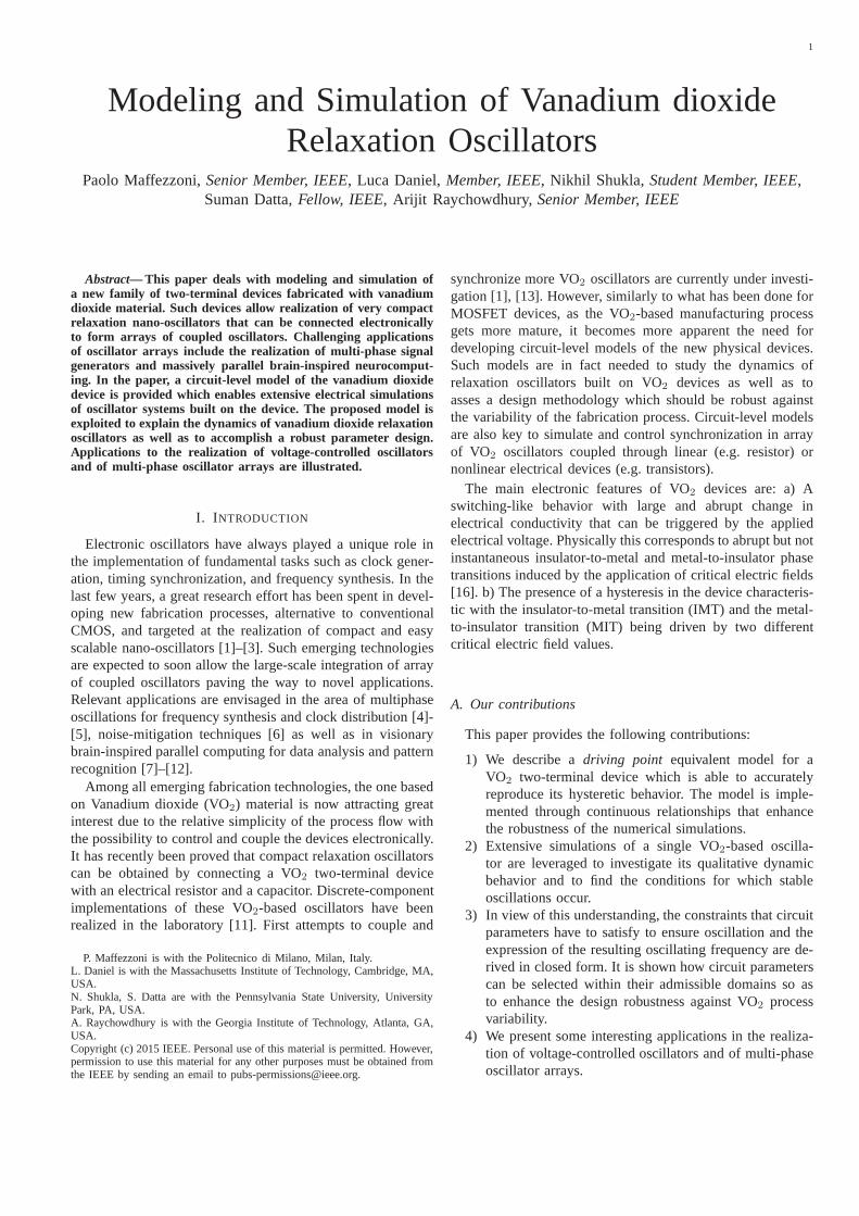
Fig. 1. I-V characteristic of a VO2 device.
B. Paper organization
This paper is divided in the following sections. In Sec. II,we describe theI-V characteristic of a VO2 device and weintroduce its circuit-level model. In Sec. III, we use simula-tions to investigate the dynamic of the oscillating mechanism.In Sec. IV, we find the closed-form constraints on circuitparameters that ensure oscillation. Finally, in Sec. V weillustrate applications.
II. C IRCUIT-LEVEL MODEL OF A VO2 DEVICE
Vanadium dioxide (VO2) is a correlated electron materialthat exhibits insulator-to-metal and metal-to-insulatorphasetransitions commonly occurring just above room temperature.The exact physics driving such transitions is still debatedwithsome authors proposing thermal mechanisms [14] [15] andsome others proposing electrical ones [16]. Independentlyofthe underlying physical mechanism, it has been shown thatsuch transitions can be triggered using various external stimuliincluding thermal [17], electrical [18], as well as opticalandmechanical. Being interested in electronic applications,inthis paper we will focus on the electrically-triggered VO2
switching-like behavior [19], [20]. The typical qualitativeshape of the electronicI-V current-voltage characteristic ofa two-terminal VO2, measured at a given environment tem-perature, is reported in Fig. 11. For relatively low currents,the device has an insulator-like behavior withV = I · Rins,whereRins is the resistance in the insulator state. When thedevice current approaches the critical valueI1, correspondingto the voltage levelVH = I1 · Rins, an IMT occurs and thecurrentI abruptly increases. This transition is abrupt but notinstantaneous with a finite intrinsic electronic switchingtime[21]. In the metallic state, we have thatV = I · Rmet with amuch smaller resistanceRmet << Rins. In this condition, tobring the device back to the insulator state, the current shouldbe reduced under the critical valueI2, corresponding to thelow voltage levelVL = I2 ·Rmet < VH , at which the inverseMIT occurs.
1The I-V characteristics are experimentally observed to be centralsym-metric with regard to the origin of coordinates, however in our applicationswe will focus on the caseV > 0.
0
1
CMP
+1 V∆V · Vo
VL
Vc
Vc
Vo
V
Vf
If
I
Rf
Ro
Co
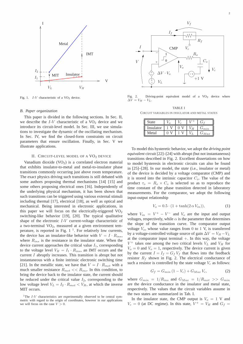
Fig. 2. Driving-point equivalent model of a VO2 device where∆V = VH − VL.
TABLE I
CIRCUIT VARIABLES IN INSULATOR AND METAL STATES
State Vo Vc V + Gf
Insulator 1 V 0 V VH Gmin
Metal 0 V 1 V VL GMax
To model this hysteretic behavior, we adopt thedriving pointequivalentcircuit [22]–[24] with abrupt (but not instantaneous)transitions described in Fig. 2. Excellent dissertations on howto model hysteresis in electronic circuits can also be foundin [25]–[28]. In our model, thestate(i.e., insulator or metal)of the device is decided by a voltage comparator (CMP) andit is stored into the intrinsic capacitorCo. The value of theproduct τo = Ro × Co is selected so as to reproduce thetime constant of the phase transition detected in laboratorymeasurements. For the comparator, we adopt the followinginput-output relationship
Vo = 0.5 · (1 + tanh(2αVin)), (1)
where Vin = V + − V − and Vo are the input and outputvoltages, respectively, whileα is the parameter that determinesthe slope of the transition curve. The comparator outputvoltageVo, whose value ranges from0 to 1 V, is transferredby a voltage-controlled voltage source of gain∆V = VH−VL
at the comparator input terminal+. In this way, the voltageV + takes one among the two critical levelsVL and VH forVo = 0 andVo = 1, respectively. The device current is givenby the currentI = If = Gf Vf that flows into the feedbackresistorRf shown in Fig. 2. The electrical conductance ofsuch a resistor is controlled by the state voltageVc as follows:
Gf = Gmin (1− Vc) +GMax Vc, (2)
where Gmin = 1/Rins and GMax = 1/Rmet >> Gmin
are the device conductance in the insulator and metal state,respectively. The values that the circuit variables assumeinthe two states are summarized in Tab. I.
In the insulator state, the CMP output isVo = 1 V andVc = 0 (at DC regime). In this state,V + = VH andGf =
3
TABLE II
DEVICE PARAMETERS
Parameter Value
Rins 50 kΩRmet 1 kΩVL 0.45VVH 6.1Vα 8τo 100 ns
I
V
Vs
Is
Rs Cs
Vdc
VO2
A
B
Fig. 3. The circuit of the relaxation oscillator.
Gmin. Hence, ifV is gradually increased until it approachesVH , it initiates an IMT. Observing thatVin = −V + VH ,Vc = 1− Vo (at DC) and in view of (1), theI-V relationshipfor values ofV close toVH becomes
I = 0.5 (GMax +Gmin) · V
+0.5 (GMax −Gmin) · V · tanh(2α (V − VH)).(3)
After the device has completed its transition to the metallicstate, the CMP output becomesVo = 0 V and Vc = 1. Inthis state,Gf = GMax andV + = VL. Thus, it is only whenV is reduced belowV + = VL that a reverse MIT can occurcompleting the cycle of the hysteresis characteristic.
The parameters of the proposed VO2-device model aresummarized in Tab. II along with the values they assume fora 2µm-length VO2 device. These parameters were extractedin the laboratory by fitting the experimental curve of thedevice. After being tuned with the experimental data of agiven VO2 device, the proposed circuit-level model is ableto realistically reproduce its electronic behavior seen attheexternal terminals. In addition, the continuous dependence ofthe electrical conductance (2) on the internal state variableVc(t) and the existence of the continuousI-V relation (3)near the transitions, give the model those regularity propertiesthat are needed for robust numerical simulations.
III. R ELAXATION OSCILLATION MECHANISM
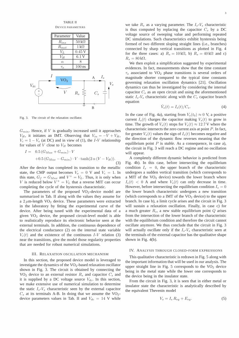
In this section, the proposed device model is leveraged toinvestigate the dynamics of the VO2-based relaxation oscillatorshown in Fig. 3. The circuit is obtained by connecting theVO2 device to an external resistorRs and capacitorCs andit is supplied by a DC voltage sourceVdc. In this section,we make extensive use of numerical simulation to determinethe staticIs-Vs characteristic seen by the external capacitorCs at its terminals A-B. In doing that we assume the VO2-device parameters values in Tab. II andVdc = 14 V while
we takeRs as a varying parameter. TheIs-Vs characteristicis thus computed by replacing the capacitorCs by a DCvoltage source of sweeping value and performing repeatedDC simulations. Such characteristics exhibit hysteresis beingformed of two different sloping straight lines (i.e., branches)connected by sharp vertical transitions as plotted in Fig. 4for the three cases: a)Rs = 10 kΩ, b) Rs = 40 kΩ and c)Rs = 80 kΩ.
We then exploit a simplification suggested by experimentalevidences. In fact, measurements show that the time constantτo associated to VO2 phase transitions is several orders ofmagnitude shorter compared to the typical time constantsgoverning relaxation oscillation dynamics [21]. Oscillationdynamics can thus be investigated by considering the internalcapacitorCo as an open circuit and using the aforementionedstaticIs-Vs characteristic along with theCs capacitor branchequation
Vs(t) = Is(t)/Cs. (4)
In the case of Fig. 4a), starting fromVs(t0) ≈ 0 V, a positivecurrentIs(t) charges the capacitor makingVs(t) to grow intime. The growth ofVs(t) stops forVs(t) ≈ 12.7V where thecharacteristic intersects the zero current axis at pointP . In fact,for greaterVs(t) values the sign ofIs(t) becomes negative andthe direction of the dynamic flow reverses meaning that theequilibrium pointP is stable. As a consequence, in case a),the circuit in Fig. 3 will reach a DC regime and no oscillationwill appear.
A completely different dynamic behavior is predicted fromFig. 4b). In this case, before intersecting the equilibriumcondition Is = 0, the upper branch of the characteristicundergoes a sudden vertical transition (which correspondstoa MIT of the VO2 device) towards the lower branch whereIs(t) < 0 A and whereVs(t) can only decrease in time.However, before intersecting the equilibrium conditionIs = 0the lower branch characteristic undergoes a new transition(which corresponds to a IMT of the VO2 device) to the upperbranch. In case b), a limit cycle arises and the circuit in Fig. 3will sustain a relaxation oscillation. Finally, in case c) fora much greaterRs, a new stable equilibrium pointQ arisesfrom the intersection of the lower branch of the characteristicwith the equilibrium condition and therefore the circuit cannotoscillate anymore. We thus conclude that the circuit in Fig.3will actually oscillate only if theIs-Vs characteristic seen atthe terminals of the external capacitor has the qualitativeshapeshown in Fig. 4(b).
IV. A NALYSIS THROUGH CLOSED-FORM EXPRESSIONS
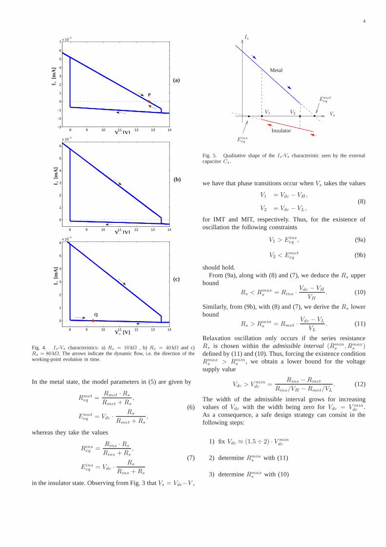
This qualitative characteristic is redrawn in Fig. 5 along withthe important information that will be used in our analysis.Theupper straight line in Fig. 5 corresponds to the VO2 devicebeing in the metal state while the lower one corresponds tothe device being in the insulator state.
From the circuit in Fig. 3, it is seen that in either metal orinsulator state the characteristic is analytically described bythe equivalent Thevenin model
Vs = Is Req + Eeq . (5)
4
8 9 10 11 12 13 14−3
−2
−1
0
1
2
3
4
5
6
7x 10
−3
(a)
P
Vs [V]
I s[m
A]
8 9 10 11 12 13 14
0
1
2
3
4
5
6
x 10−3
(b)
Vs [V]
I s[m
A]
8 9 10 11 12 13 14
0
1
2
3
4
5
6x 10
−3
(c)
Q
Vs [V]
I s[m
A]
Fig. 4. Is-Vs characteristics: a)Rs = 10 kΩ , b) Rs = 40 kΩ and c)Rs = 80 kΩ. The arrows indicate the dynamic flow, i.e. the direction of theworking-point evolution in time.
In the metal state, the model parameters in (5) are given by
Rmeteq =
Rmet ·Rs
Rmet +Rs
,
Emeteq = Vdc ·
Rs
Rmet +Rs
,
(6)
whereas they take the values
Rinseq =
Rins · Rs
Rins +Rs
,
Einseq = Vdc ·
Rs
Rins +Rs
(7)
in the insulator state. Observing from Fig. 3 thatVs = Vdc−V ,
Vs
Is
V1 V2
Einseq
Emeteq
Metal
Insulator
Fig. 5. Qualitative shape of theIs-Vs characteristic seen by the externalcapacitorCs.
we have that phase transitions occur whenVs takes the values
V1 = Vdc − VH ,
V2 = Vdc − VL,(8)
for IMT and MIT, respectively. Thus, for the existence ofoscillation the following constraints
V1 > Einseq , (9a)
V2 < Emeteq (9b)
should hold.From (9a), along with (8) and (7), we deduce theRs upper
bound
Rs < Rmaxs = Rins ·
Vdc − VH
VH
. (10)
Similarly, from (9b), with (8) and (7), we derive theRs lowerbound
Rs > Rmins = Rmet ·
Vdc − VL
VL
. (11)
Relaxation oscillation only occurs if the series resistanceRs is chosen within theadmissible interval(Rmin
s , Rmaxs )
defined by (11) and (10). Thus, forcing the existence conditionRmax
s > Rmins , we obtain a lower bound for the voltage
supply value
Vdc > V mindc =
Rins −Rmet
Rins/VH −Rmet/VL
. (12)
The width of the admissible interval grows for increasingvalues ofVdc with the width being zero forVdc = V min
dc .As a consequence, a safe design strategy can consist in thefollowing steps:
1) fix Vdc ≈ (1.5÷ 2) · Vmindc
2) determineRmins with (11)
3) determineRmaxs with (10)
5
Einseq
Emeteq
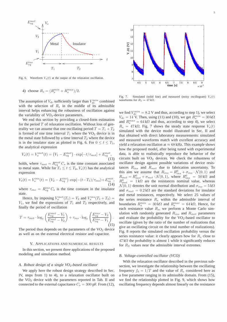
t
Vs
T1 T2
V1
V2
Metal Insulator
Fig. 6. WaveformVs(t) at the output of the relaxation oscillation.
4) chooseRs = (Rmins +Rmax
s )/2.
The assumption ofVdc sufficiently larger thanV mindc combined
with the selection ofRs in the middle of its admissibleinterval helps enhancing the robustness of oscillation againstthe variability of VO2-device parameters.
We end this section by providing a closed-form estimationfor the periodT of relaxation oscillation. Without loss of gen-erality we can assume that one oscillating periodT = T1 + T2
is formed of one time intervalT1 where the VO2 device is inthe metal state followed by a time intervalT2 where the deviceis in the insulator state as plotted in Fig. 6. For0 ≤ t ≤ T1,the analytical expression
Vs(t) = V mets (t) =
(
V1 − Emeteq
)
· exp[−t/τmet] + Emeteq ,
(13)holds, whereτmet = Rmet
eq Cs is the time constant associatedto metal state. While forT1 ≤ t ≤ T2, Vs(t) has the analyticalexpression
Vs(t) = V inss (t) =
(
V2 − Einseq
)
·exp[−(t−T1)/τins)+Emeteq ,(14)
where τins = Rinseq Cs is the time constant in the insulator
state.Hence, by imposingV met
s (T1) = V2 andV inss (T1 + T2) =
V1, we find the expressions ofT1 and T2 respectively, andfinally the period of oscillation
T = τmet · loge
(
Emeteq − V1
Emeteq − V2
)
+ τins · loge
(
Einseq − V2
Einseq − V1
)
.
(15)The period thus depends on the parameters of the VO2 deviceas well as on the external electrical resistor and capacitor.
V. A PPLICATIONS AND NUMERICAL RESULTS
In this section, we present three applications of the proposedmodeling and simulation method.
A. Robust design of a single VO2-based oscillator
We apply here the robust design strategy described in Sec.IV, steps from 1) to 4), to a relaxation oscillator built onthe VO2 device with the parameters reported in Tab. II andconnected to the external capacitanceCs = 300 pF. From (12),
4.5 5 5.5 6 6.5 7 7.5 8 8.5 9
x 10−5
7
8
9
10
11
12
13
14
time [s]
Vs(t
)[V
]
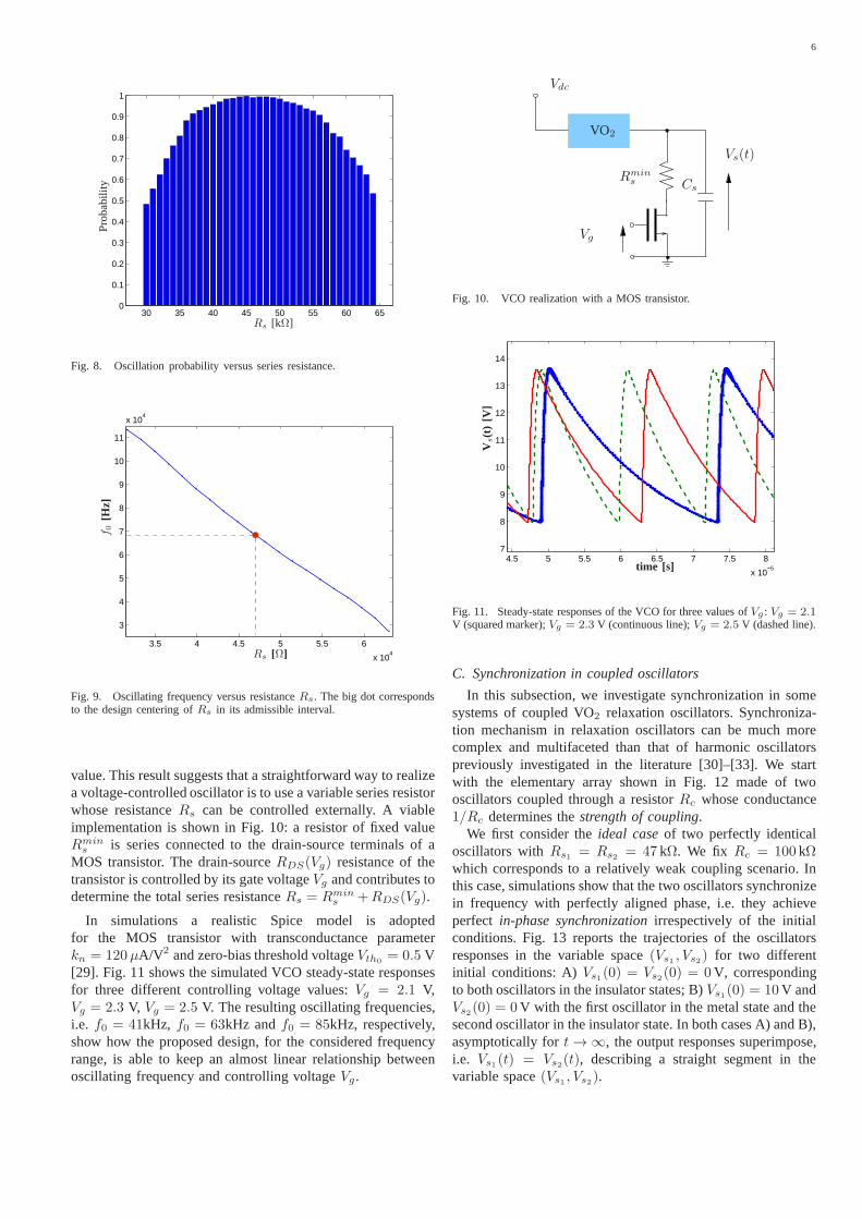
Fig. 7. Simulated (solid line) and measured (noisy oscillogram) Vs(t)waveforms forRs = 47 kΩ.
we findV mindc = 8.2 V and thus, according to step 1), we select
Vdc = 14 V. Then, using (11) and (10), we getRmins = 30 kΩ
andRmaxs = 64 kΩ and thus, according to step 4), we select
Rs = 47 kΩ. Fig. 7 shows the steady state responseVs(t)simulated with the device model illustrated in Sec. II andthat obtained with direct laboratory measurements: simulatedand measured waveforms match with excellent accuracy andyield a relaxation oscillation at≈ 68 kHz. This example showshow the proposed model, after being tuned with experimentaldata, is able to realistically reproduce the behavior of thecircuits built on VO2 devices. We check the robustness ofoscillator design against possible variations of device resis-tancesRins and Rmet due to fabrication uncertainty. Tothis aim we assume thatRins = R0
ins + σins · N (0, 1) andRmet = R0
met + σmet · N (0, 1), where R0ins = 50 kΩ and
R0met = 1 kΩ are the resistances nominal value, whereas
N (0, 1) denotes the unit normal distribution andσins = 5 kΩand σmet = 0.2 kΩ are the standard deviations for insulatorand metal resistances, respectively. We select 25 values ofthe series resistanceRs within the admissible interval ofboundariesRmin
s = 30 kΩ and Rmaxs = 64 kΩ. Hence, for
each resistance valueRs, we perform a Monte Carlo sim-ulation with randomly generatedRins andRmet parametersand evaluate the probability for the VO2-based oscillator tooscillate (given by the ratio of the number of realizations thatgive an oscillating circuit on the total number of realizations).Fig. 8 reports the simulated oscillation probability versus theseries resistance value: it clearly appears how forRs close to47 kΩ the probability is almost 1 while it significantly reducesfor RS values near the admissible interval extremes.
B. Voltage-controlled oscillator (VCO)
With the relaxation oscillator described in the previous sub-section, we investigate the relationship between the oscillatingfrequencyf0 = 1/T and the value ofRs considered here asa free parameter ranging in its admissible domain. From (15),we find the relationship plotted in Fig. 9, which shows howoscillating frequency depends almost linearly on the resistance
6
30 35 40 45 50 55 60 650
0.1
0.2
0.3
0.4
0.5
0.6
0.7
0.8
0.9
1
Rs [kΩ]
Pro
bab
ility
Fig. 8. Oscillation probability versus series resistance.
3.5 4 4.5 5 5.5 6
x 104
3
4
5
6
7
8
9
10
11
x 104
Rs [Ω]
f 0[H
z]
Fig. 9. Oscillating frequency versus resistanceRs. The big dot correspondsto the design centering ofRs in its admissible interval.
value. This result suggests that a straightforward way to realizea voltage-controlled oscillator is to use a variable seriesresistorwhose resistanceRs can be controlled externally. A viableimplementation is shown in Fig. 10: a resistor of fixed valueRmin
s is series connected to the drain-source terminals of aMOS transistor. The drain-sourceRDS(Vg) resistance of thetransistor is controlled by its gate voltageVg and contributes todetermine the total series resistanceRs = Rmin
s +RDS(Vg).
In simulations a realistic Spice model is adoptedfor the MOS transistor with transconductance parameterkn = 120µA/V2 and zero-bias threshold voltageVth0
= 0.5 V[29]. Fig. 11 shows the simulated VCO steady-state responsesfor three different controlling voltage values:Vg = 2.1 V,Vg = 2.3 V, Vg = 2.5 V. The resulting oscillating frequencies,i.e. f0 = 41kHz, f0 = 63kHz andf0 = 85kHz, respectively,show how the proposed design, for the considered frequencyrange, is able to keep an almost linear relationship betweenoscillating frequency and controlling voltageVg.
Vg
Vs(t)
Rmins Cs
Vdc
VO2
Fig. 10. VCO realization with a MOS transistor.
4.5 5 5.5 6 6.5 7 7.5 8
x 10−5
7
8
9
10
11
12
13
14
time [s]
Vs(t
)[V
]
Fig. 11. Steady-state responses of the VCO for three values of Vg : Vg = 2.1V (squared marker);Vg = 2.3 V (continuous line);Vg = 2.5 V (dashed line).
C. Synchronization in coupled oscillators
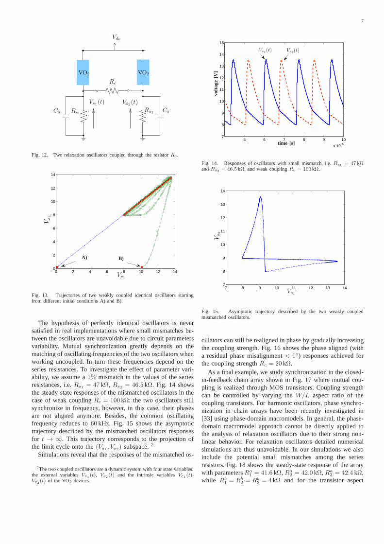
In this subsection, we investigate synchronization in somesystems of coupled VO2 relaxation oscillators. Synchroniza-tion mechanism in relaxation oscillators can be much morecomplex and multifaceted than that of harmonic oscillatorspreviously investigated in the literature [30]–[33]. We startwith the elementary array shown in Fig. 12 made of twooscillators coupled through a resistorRc whose conductance1/Rc determines thestrength of coupling.
We first consider theideal caseof two perfectly identicaloscillators withRs1 = Rs2 = 47 kΩ. We fix Rc = 100 kΩwhich corresponds to a relatively weak coupling scenario. Inthis case, simulations show that the two oscillators synchronizein frequency with perfectly aligned phase, i.e. they achieveperfect in-phase synchronizationirrespectively of the initialconditions. Fig. 13 reports the trajectories of the oscillatorsresponses in the variable space(Vs1 , Vs2) for two differentinitial conditions: A) Vs1(0) = Vs2(0) = 0V, correspondingto both oscillators in the insulator states; B)Vs1(0) = 10V andVs2(0) = 0V with the first oscillator in the metal state and thesecond oscillator in the insulator state. In both cases A) and B),asymptotically fort → ∞, the output responses superimpose,i.e. Vs1 (t) = Vs2(t), describing a straight segment in thevariable space(Vs1 , Vs2).
7
Rc
Vs2(t)
Rs2
Vs1(t)
Rs1CsCs
Vdc
VO2VO2
Fig. 12. Two relaxation oscillators coupled through the resistor Rc.
0 2 4 6 8 10 12 140
2
4
6
8
10
12
14
A) B)
Vs1
Vs2
Fig. 13. Trajectories of two weakly coupled identical oscillators startingfrom different initial conditions A) and B).
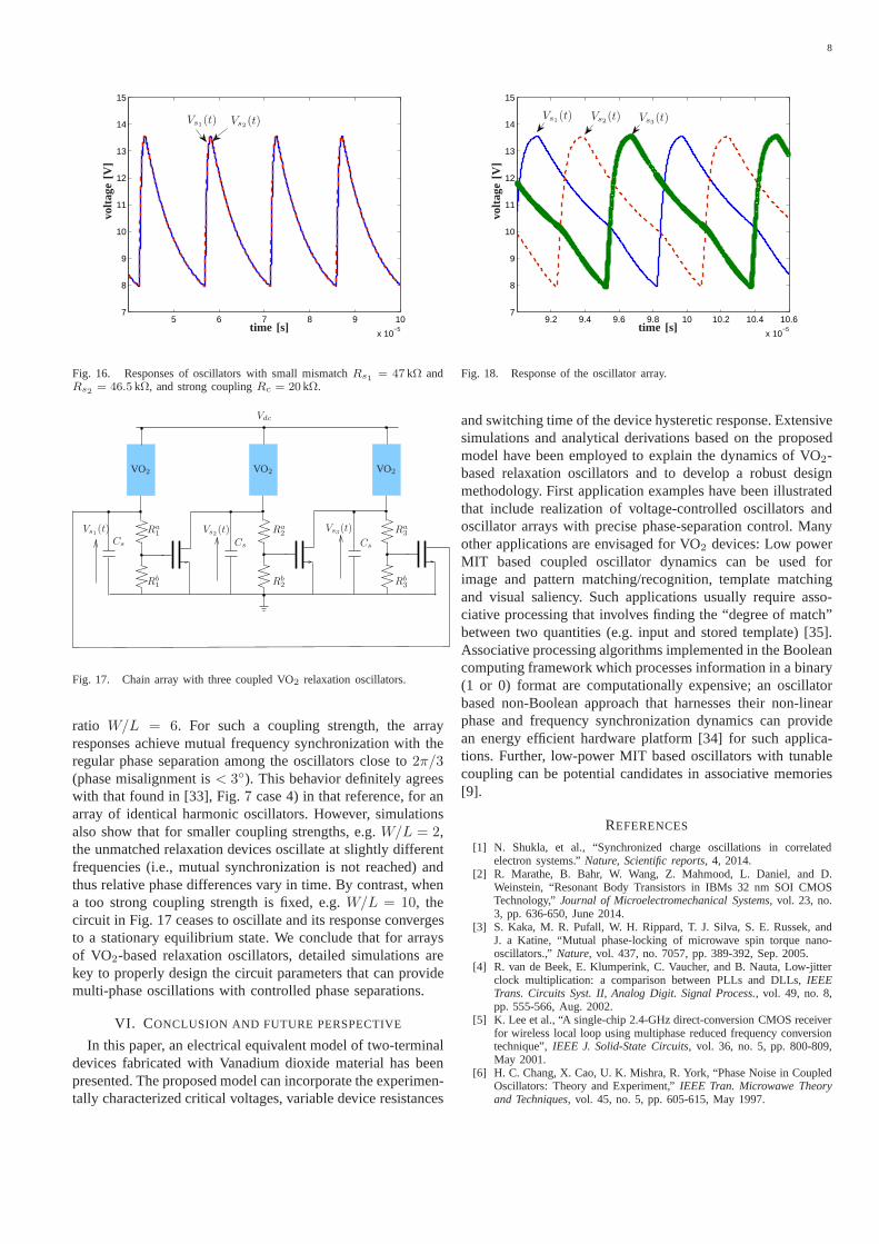
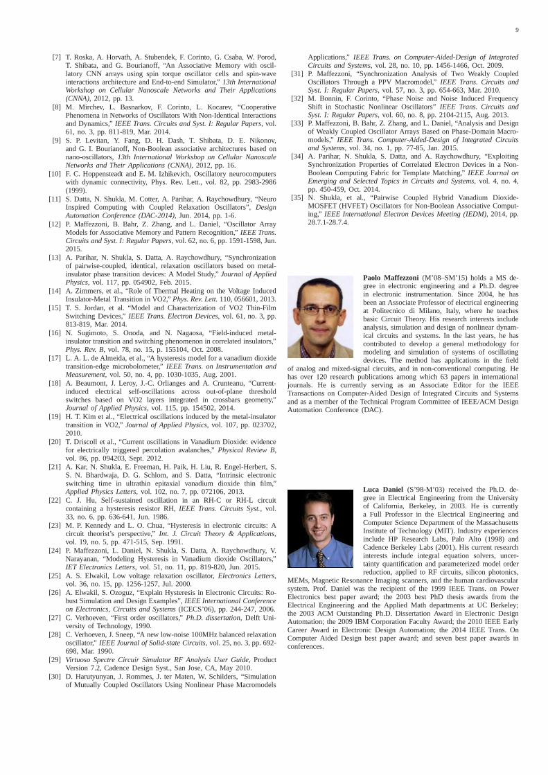
The hypothesis of perfectly identical oscillators is neversatisfied in real implementations where small mismatches be-tween the oscillators are unavoidable due to circuit parametersvariability. Mutual synchronization greatly depends on thematching of oscillating frequencies of the two oscillatorswhenworking uncoupled. In turn these frequencies depend on theseries resistances. To investigate the effect of parametervari-ability, we assume a1% mismatch in the values of the seriesresistances, i.e.Rs1 = 47 kΩ, Rs2 = 46.5 kΩ. Fig. 14 showsthe steady-state responses of the mismatched oscillators in thecase of weak couplingRc = 100 kΩ: the two oscillators stillsynchronize in frequency, however, in this case, their phasesare not aligned anymore. Besides, the common oscillatingfrequency reduces to60 kHz. Fig. 15 shows the asymptotictrajectory described by the mismatched oscillators responsesfor t → ∞. This trajectory corresponds to the projection ofthe limit cycle onto the(Vs1 , Vs2) subspace.2
Simulations reveal that the responses of the mismatched os-
2The two coupled oscillators are a dynamic system with four state variables:the external variablesVs1 (t), Vs2 (t) and the intrinsic variablesVc1(t),Vc2(t) of the VO2 devices.
5 6 7 8 9 10
x 10−5
7
8
9
10
11
12
13
14
15
time [s]
volta
ge[V
]
Vs1 (t) Vs2(t)
Fig. 14. Responses of oscillators with small mismatch, i.e.Rs1 = 47 kΩandRs2 = 46.5 kΩ, and weak couplingRc = 100 kΩ.
7 8 9 10 11 12 13 147
8
9
10
11
12
13
14
Vs1
Vs2
Fig. 15. Asymptotic trajectory described by the two weakly coupledmismatched oscillators.
cillators can still be realigned in phase by gradually increasingthe coupling strength. Fig. 16 shows the phase aligned (witha residual phase misalignment< 1) responses achieved forthe coupling strengthRc = 20 kΩ.
As a final example, we study synchronization in the closed-in-feedback chain array shown in Fig. 17 where mutual cou-pling is realized through MOS transistors. Coupling strengthcan be controlled by varying theW/L aspect ratio of thecoupling transistors. For harmonic oscillators, phase synchro-nization in chain arrays have been recently investigated in[33] using phase-domain macromodels. In general, the phase-domain macromodel approach cannot be directly applied tothe analysis of relaxation oscillators due to their strong non-linear behavior. For relaxation oscillators detailed numericalsimulations are thus unavoidable. In our simulations we alsoinclude the potential small mismatches among the seriesresistors. Fig. 18 shows the steady-state response of the arraywith parametersRa
1 = 41.6 kΩ, Ra2 = 42.0 kΩ, Ra
3 = 42.4 kΩ,while Rb
1 = Rb2 = Rb
3 = 4 kΩ and for the transistor aspect
8
5 6 7 8 9 10
x 10−5
7
8
9
10
11
12
13
14
15
time [s]
volta
ge[V
]Vs1(t) Vs2 (t)
Fig. 16. Responses of oscillators with small mismatchRs1 = 47 kΩ andRs2 = 46.5 kΩ, and strong couplingRc = 20 kΩ.
Vs3(t)Vs2(t) Ra3
Rb3
Ra2
Rb2
Ra1
Rb1
Vs1(t)
CsCsCs
Vdc
VO2 VO2VO2
Fig. 17. Chain array with three coupled VO2 relaxation oscillators.
ratio W/L = 6. For such a coupling strength, the arrayresponses achieve mutual frequency synchronization with theregular phase separation among the oscillators close to2π/3(phase misalignment is< 3). This behavior definitely agreeswith that found in [33], Fig.7 case 4) in that reference, for anarray of identical harmonic oscillators. However, simulationsalso show that for smaller coupling strengths, e.g.W/L = 2,the unmatched relaxation devices oscillate at slightly differentfrequencies (i.e., mutual synchronization is not reached)andthus relative phase differences vary in time. By contrast, whena too strong coupling strength is fixed, e.g.W/L = 10, thecircuit in Fig. 17 ceases to oscillate and its response convergesto a stationary equilibrium state. We conclude that for arraysof VO2-based relaxation oscillators, detailed simulations arekey to properly design the circuit parameters that can providemulti-phase oscillations with controlled phase separations.
VI. CONCLUSION AND FUTURE PERSPECTIVE
In this paper, an electrical equivalent model of two-terminaldevices fabricated with Vanadium dioxide material has beenpresented. The proposed model can incorporate the experimen-tally characterized critical voltages, variable device resistances
9.2 9.4 9.6 9.8 10 10.2 10.4 10.6
x 10−5
7
8
9
10
11
12
13
14
15
time [s]
volta
ge[V
]
Vs1(t) Vs2(t) Vs3(t)
Fig. 18. Response of the oscillator array.
and switching time of the device hysteretic response. Extensivesimulations and analytical derivations based on the proposedmodel have been employed to explain the dynamics of VO2-based relaxation oscillators and to develop a robust designmethodology. First application examples have been illustratedthat include realization of voltage-controlled oscillators andoscillator arrays with precise phase-separation control.Manyother applications are envisaged for VO2 devices: Low powerMIT based coupled oscillator dynamics can be used forimage and pattern matching/recognition, template matchingand visual saliency. Such applications usually require asso-ciative processing that involves finding the “degree of match”between two quantities (e.g. input and stored template) [35].Associative processing algorithms implemented in the Booleancomputing framework which processes information in a binary(1 or 0) format are computationally expensive; an oscillatorbased non-Boolean approach that harnesses their non-linearphase and frequency synchronization dynamics can providean energy efficient hardware platform [34] for such applica-tions. Further, low-power MIT based oscillators with tunablecoupling can be potential candidates in associative memories[9].
REFERENCES
[1] N. Shukla, et al., “Synchronized charge oscillations incorrelatedelectron systems.”Nature, Scientific reports, 4, 2014.
[2] R. Marathe, B. Bahr, W. Wang, Z. Mahmood, L. Daniel, and D.Weinstein, “Resonant Body Transistors in IBMs 32 nm SOI CMOSTechnology,”Journal of Microelectromechanical Systems, vol. 23, no.3, pp. 636-650, June 2014.
[3] S. Kaka, M. R. Pufall, W. H. Rippard, T. J. Silva, S. E. Russek, andJ. a Katine, “Mutual phase-locking of microwave spin torquenano-oscillators.,”Nature, vol. 437, no. 7057, pp. 389-392, Sep. 2005.
[4] R. van de Beek, E. Klumperink, C. Vaucher, and B. Nauta, Low-jitterclock multiplication: a comparison between PLLs and DLLs,IEEETrans. Circuits Syst. II, Analog Digit. Signal Process., vol. 49, no. 8,pp. 555-566, Aug. 2002.
[5] K. Lee et al., “A single-chip 2.4-GHz direct-conversionCMOS receiverfor wireless local loop using multiphase reduced frequencyconversiontechnique”,IEEE J. Solid-State Circuits, vol. 36, no. 5, pp. 800-809,May 2001.
[6] H. C. Chang, X. Cao, U. K. Mishra, R. York, “Phase Noise in CoupledOscillators: Theory and Experiment,”IEEE Tran. Microwawe Theoryand Techniques, vol. 45, no. 5, pp. 605-615, May 1997.
9
[7] T. Roska, A. Horvath, A. Stubendek, F. Corinto, G. Csaba,W. Porod,T. Shibata, and G. Bourianoff, “An Associative Memory with oscil-latory CNN arrays using spin torque oscillator cells and spin-waveinteractions architecture and End-to-end Simulator,”13th InternationalWorkshop on Cellular Nanoscale Networks and Their Applications(CNNA), 2012, pp. 13.
[8] M. Mirchev, L. Basnarkov, F. Corinto, L. Kocarev, “CooperativePhenomena in Networks of Oscillators With Non-Identical Interactionsand Dynamics,”IEEE Trans. Circuits and Syst. I: Regular Papers, vol.61, no. 3, pp. 811-819, Mar. 2014.
[9] S. P. Levitan, Y. Fang, D. H. Dash, T. Shibata, D. E. Nikonov,and G. I. Bourianoff, Non-Boolean associative architectures based onnano-oscillators,13th International Workshop on Cellular NanoscaleNetworks and Their Applications (CNNA), 2012, pp. 16.
[10] F. C. Hoppensteadt and E. M. Izhikevich, Oscillatory neurocomputerswith dynamic connectivity, Phys. Rev. Lett., vol. 82, pp. 2983-2986(1999).
[11] S. Datta, N. Shukla, M. Cotter, A. Parihar, A. Raychowdhury, “NeuroInspired Computing with Coupled Relaxation Oscillators”,DesignAutomation Conference (DAC-2014), Jun. 2014, pp. 1-6.
[12] P. Maffezzoni, B. Bahr, Z. Zhang, and L. Daniel, “Oscillator ArrayModels for Associative Memory and Pattern Recognition,”IEEE Trans.Circuits and Syst. I: Regular Papers, vol. 62, no. 6, pp. 1591-1598, Jun.2015.
[13] A. Parihar, N. Shukla, S. Datta, A. Raychowdhury, “Synchronizationof pairwise-coupled, identical, relaxation oscillators based on metal-insulator phase transition devices: A Model Study,”Journal of AppliedPhysics, vol. 117, pp. 054902, Feb. 2015.
[14] A. Zimmers, et al., “Role of Thermal Heating on the Voltage InducedInsulator-Metal Transition in VO2,”Phys. Rev. Lett.110, 056601, 2013.
[15] T. S. Jordan, et al. “Model and Characterization of VO2 Thin-FilmSwitching Devices,”IEEE Trans. Electron Devices, vol. 61, no. 3, pp.813-819, Mar. 2014.
[16] N. Sugimoto, S. Onoda, and N. Nagaosa, “Field-induced metal-insulator transition and switching phenomenon in correlated insulators,”Phys. Rev. B, vol. 78, no. 15, p. 155104, Oct. 2008.
[17] L. A. L. de Almeida, et al., “A hysteresis model for a vanadium dioxidetransition-edge microbolometer,”IEEE Trans. on Instrumentation andMeasurement, vol. 50, no. 4, pp. 1030-1035, Aug. 2001.
[18] A. Beaumont, J. Leroy, J.-C. Orlianges and A. Crunteanu, “Current-induced electrical self-oscillations across out-of-plane thresholdswitches based on VO2 layers integrated in crossbars geometry,”Journal of Applied Physics, vol. 115, pp. 154502, 2014.
[19] H. T. Kim et al., “Electrical oscillations induced by the metal-insulatortransition in VO2,”Journal of Applied Physics, vol. 107, pp. 023702,2010.
[20] T. Driscoll et al., “Current oscillations in Vanadium Dioxide: evidencefor electrically triggered percolation avalanches,”Physical Review B,vol. 86, pp. 094203, Sept. 2012.
[21] A. Kar, N. Shukla, E. Freeman, H. Paik, H. Liu, R. Engel-Herbert, S.S. N. Bhardwaja, D. G. Schlom, and S. Datta, “Intrinsic electronicswitching time in ultrathin epitaxial vanadium dioxide thin film,”Applied Physics Letters, vol. 102, no. 7, pp. 072106, 2013.
[22] C. J. Hu, Self-sustained oscillation in an RH-C or RH-L circuitcontaining a hysteresis resistor RH,IEEE Trans. Circuits Syst., vol.33, no. 6, pp. 636-641, Jun. 1986.
[23] M. P. Kennedy and L. O. Chua, “Hysteresis in electronic circuits: Acircuit theorist’s perspective,”Int. J. Circuit Theory & Applications,vol. 19, no. 5, pp. 471-515, Sep. 1991.
[24] P. Maffezzoni, L. Daniel, N. Shukla, S. Datta, A. Raychowdhury, V.Narayanan, “Modeling Hysteresis in Vanadium dioxide Oscillators,”IET Electronics Letters, vol. 51, no. 11, pp. 819-820, Jun. 2015.
[25] A. S. Elwakil, Low voltage relaxation oscillator,Electronics Letters,vol. 36, no. 15, pp. 1256-1257, Jul. 2000.
[26] A. Elwakil, S. Ozoguz, “Explain Hysteresis in Electronic Circuits: Ro-bust Simulation and Design Examples”,IEEE International Conferenceon Electronics, Circuits and Systems(ICECS’06), pp. 244-247, 2006.
[27] C. Verhoeven, “First order oscillators,”Ph.D. dissertation, Delft Uni-versity of Technology, 1990.
[28] C. Verhoeven, J. Sneep, “A new low-noise 100MHz balanced relaxationoscillator,” IEEE Journal of Solid-state Circuits, vol. 25, no. 3, pp. 692-698, Mar. 1990.
[29] Virtuoso Spectre Circuir Simulator RF Analysis User Guide, ProductVersion 7.2, Cadence Design Syst., San Jose, CA, May 2010.
[30] D. Harutyunyan, J. Rommes, J. ter Maten, W. Schilders, “Simulationof Mutually Coupled Oscillators Using Nonlinear Phase Macromodels
Applications,” IEEE Trans. on Computer-Aided-Design of IntegratedCircuits and Systems, vol. 28, no. 10, pp. 1456-1466, Oct. 2009.
[31] P. Maffezzoni, “Synchronization Analysis of Two Weakly CoupledOscillators Through a PPV Macromodel,”IEEE Trans. Circuits andSyst. I: Regular Papers, vol. 57, no. 3, pp. 654-663, Mar. 2010.
[32] M. Bonnin, F. Corinto, “Phase Noise and Noise Induced FrequencyShift in Stochastic Nonlinear Oscillators”IEEE Trans. Circuits andSyst. I: Regular Papers, vol. 60, no. 8, pp. 2104-2115, Aug. 2013.
[33] P. Maffezzoni, B. Bahr, Z. Zhang, and L. Daniel, “Analysis and Designof Weakly Coupled Oscillator Arrays Based on Phase-Domain Macro-models,” IEEE Trans. Computer-Aided-Design of Integrated Circuitsand Systems, vol. 34, no. 1, pp. 77-85, Jan. 2015.
[34] A. Parihar, N. Shukla, S. Datta, and A. Raychowdhury, “ExploitingSynchronization Properties of Correlated Electron Devices in a Non-Boolean Computing Fabric for Template Matching,”IEEE Journal onEmerging and Selected Topics in Circuits and Systems, vol. 4, no. 4,pp. 450-459, Oct. 2014.
[35] N. Shukla, et al., “Pairwise Coupled Hybrid Vanadium Dioxide-MOSFET (HVFET) Oscillators for Non-Boolean Associative Comput-ing,” IEEE International Electron Devices Meeting (IEDM), 2014, pp.28.7.1-28.7.4.
Paolo Maffezzoni (M’08–SM’15) holds a MS de-gree in electronic engineering and a Ph.D. degreein electronic instrumentation. Since 2004, he hasbeen an Associate Professor of electrical engineeringat Politecnico di Milano, Italy, where he teachesbasic Circuit Theory. His research interests includeanalysis, simulation and design of nonlinear dynam-ical circuits and systems. In the last years, he hascontributed to develop a general methodology formodeling and simulation of systems of oscillatingdevices. The method has applications in the field
of analog and mixed-signal circuits, and in non-conventional computing. Hehas over 120 research publications among which 63 papers in internationaljournals. He is currently serving as an Associate Editor forthe IEEETransactions on Computer-Aided Design of Integrated Circuits and Systemsand as a member of the Technical Program Committee of IEEE/ACM DesignAutomation Conference (DAC).
Luca Daniel (S’98-M’03) received the Ph.D. de-gree in Electrical Engineering from the Universityof California, Berkeley, in 2003. He is currentlya Full Professor in the Electrical Engineering andComputer Science Department of the MassachusettsInstitute of Technology (MIT). Industry experiencesinclude HP Research Labs, Palo Alto (1998) andCadence Berkeley Labs (2001). His current researchinterests include integral equation solvers, uncer-tainty quantification and parameterized model orderreduction, applied to RF circuits, silicon photonics,
MEMs, Magnetic Resonance Imaging scanners, and the human cardiovascularsystem. Prof. Daniel was the recipient of the 1999 IEEE Trans. on PowerElectronics best paper award; the 2003 best PhD thesis awards from theElectrical Engineering and the Applied Math departments atUC Berkeley;the 2003 ACM Outstanding Ph.D. Dissertation Award in Electronic DesignAutomation; the 2009 IBM Corporation Faculty Award; the 2010 IEEE EarlyCareer Award in Electronic Design Automation; the 2014 IEEETrans. OnComputer Aided Design best paper award; and seven best paperawards inconferences.
10
Nikhil Shukla received the B.S. degree in electron-ics and telecommunications engineering from theUniversity of Mumbai, Mumbai, India, in 2010. Heis currently working toward the Ph.D. degree inelectrical engineering in the Department of Electri-cal Engineering, The Pennsylvania State University,University Park, PA, USA.
Suman Datta (F13) received the B.S. degree inelectrical engineering from the Indian Institute ofTechnology, Kanpur, India, in 1995, and the Ph.D.degree in electrical and computer engineering fromthe University of Cincinnati, Cincinnati, OH, USA,in 1999. From 1999 to 2007, he was a memberof the Logic Technology Development Group, IntelCorporation. He was instrumental in the demonstra-tion of III-V quantum-well transistors operating atroom temperature with a record energy delay prod-uct, the first experimental demonstration of high-
performance high-k/metal gate CMOS transistors, and the invention anddemonstration nonplanar trigate transistors. In 2007, he was the JosephMonkowski Associate Professor of Electrical Engineering with PennsylvaniaState University, University Park, PA, USA, where he is currently a Professorof Electrical Engineering. He is the holder of more than 160 U.S. patents.His group is exploring new materials and novel device architecture forCMOS enhancement and replacement for future energy-efficient computingapplications. Dr. Datta is a Distinguished Lecturer of the IEEE ElectronDevices Society.
Arijit Raychowdhury (M07–SM13) received theB.E. degree in electrical and telecommunication en-gineering from Jadavpur University, Kolkata, India,and the Ph.D. degree in electrical and computerengineering from Purdue University, West Lafayette,IN, USA. He is currently an Associate Professor inthe School of Electrical and Computer Engineering,Georgia Institute of Technology, Atlanta, GA, USA,where he joined in January, 2013. His industryexperience includes five years as a Staff Scientistin the Circuits Research Lab, Intel Corporation and
a year as an Analog Circuit Designer with Texas Instruments Inc. Hisresearch interests include digital and mixed-signal circuit design, design ofon-chip sensors, memory, and device-circuit interactions. He holds more than25 U.S. and international patents and has published over 100articles injournals and refereed conferences. Dr. Raychowdhury is thewinner of theIntel Labs Technical Contribution Award, 2011; Dimitris N.Chorafas Awardfor outstanding doctoral research, 2007; the Best Thesis Award, College ofEngineering, Purdue University, 2007; Best Paper Awards atthe InternationalSymposium on Low Power Electronic Design (ISLPED) 2012, 2006; IEEENanotechnology Conference, 2003; SRC Technical Excellence Award, 2005;Intel Foundation Fellowship 2006, NASA INAC Fellowship 2004, and theMeissner Fellowship 2002.