Embed Size (px)
Citation preview
Microelectronics Reliability 50 (2010) 1021–1027
Contents lists available at ScienceDirect
Microelectronics Reliability
journal homepage: www.elsevier .com/locate /microrel
Modeling of board-level package by Finite Element Analysis and laserinterferometer measurements
Bo Zhang a, Pin-kuan Liu a,*, Han Ding a, Wenwu Cao b
a State Key Laboratory of Mechanical System and Vibration, School of Mechanical Engineering, Shanghai Jiao Tong University, 800 Dong Chuan Road, Shanghai 200240, Chinab Materials Research Institute, The Pennsylvania State University, University Park, PA 16802, USA
a r t i c l e i n f o
Article history:Received 12 November 2009Received in revised form 16 March 2010
0026-2714/$ - see front matter Crown Copyright � 2doi:10.1016/j.microrel.2010.03.009
* Corresponding author. Tel./fax: +86 21 34207143E-mail address: [email protected] (P.-k. Liu).
a b s t r a c t
Board-level package is a complicated multi-components structure. It can be simulated by an equivalentFinite Element Analysis (FEA) model of the board-level package, in which detailed layer structure of thePrint Circuit Board (PCB), signal wires and through-holes were ignored. For this purpose, it is necessary toobtain the equivalent material properties of the board-level package. In this work, a laser-based interfer-ometric technique was used to measure the modal parameters of the board-level package. By fitting theFEA results with the experimental results, we can obtain equivalent material properties of the board-levelpackage by means of the Taguchi method. Four control factors (Young’s modulus in the x and y direction,mass density and shear modulus in the xy plane) at three levels are explored and assigned to the columnsof a L9(34) saturated orthogonal array. The so obtained equivalent parameters provided the best fitbetween the FEA results and the experimental observations.
Crown Copyright � 2010 Published by Elsevier Ltd. All rights reserved.
1. Introduction
Multi-functionalities and miniaturization of portable electronicproducts make the anti-drop performance of solder interconnec-tions a vital issue in modern electronic industry. It is difficult tomeasure the dynamic response of solder interconnections duringdrop tests due to their small dimension and fine pitch. Finite Ele-ment Analysis (FEA) has been proven an effective way to studythe dynamic stress and strain response of the solder interconnec-tions [1–9].
However, it is difficult to build a detailed finite element (FE)model of the board-level package due to the complicated structureinvolved, such as the layer structure, through-holes and signalwires of the Print Circuit Board (PCB). In order to reduce the sizeof the FE model, it is necessary to build an equivalent FE modelwith equivalent material properties. The accuracy of the FEA solu-tion greatly depends on the input equivalent material properties ofthe board-level package.
Modal analysis is the base for the analysis of the dynamic re-sponse of the board-level package when mode superposition meth-od is adopted. The inherent properties of the board-level package,including modal deflection contour, natural frequency and struc-tural damping, can be obtained by Experimental Modal Analysis(EMA). The EMA results can be used to verify the equivalent FE
010 Published by Elsevier Ltd. All r
.
model of the board-level package and optimize the equivalentmaterial properties.
Modal analysis of board-level package had been studied by thehammer method. Lee et al. [10] performed the EMA to establish anequivalent FE model for the dynamic response analysis of theboard-level package. Zhang et al. [11] also carried out the modalanalysis of the board-level package by theoretical and experimen-tal analyses. However, the added-mass of the accelerometer andhammer greatly decreased the test accuracy because the added-mass cannot be ignored compared to the mass of the board-levelpackage. In addition, due to the low stiffness coefficient of theboard-level package, it is difficult to obtain a good coherence func-tion at some positions (e.g., the edge of board-level package). Thenarrow bandwidth of the input pulse by the hammer also leadsto poor coherence functions in the high frequency region. On theother hand, the laser-based interferometric technique is a non-contact, full-field and real-time test method [12], and thus a muchbetter method for the modal parameter test of small and lightobjects.
In this paper, we used the laser-based interferometric techniqueto measure the modal parameters of the board-level package withtwo opposed edges fixed and another two opposed edges free. Themode shapes and natural frequencies of the board-level packagewere experimentally measured using Optonor VibroMap 1000 sys-tem based on the technology of TV-holography. The equivalent FEmodel of the board-level package was built using ANSYS and theequivalent material properties were obtained by optimizing thematching between FEA and EMA results.
ights reserved.
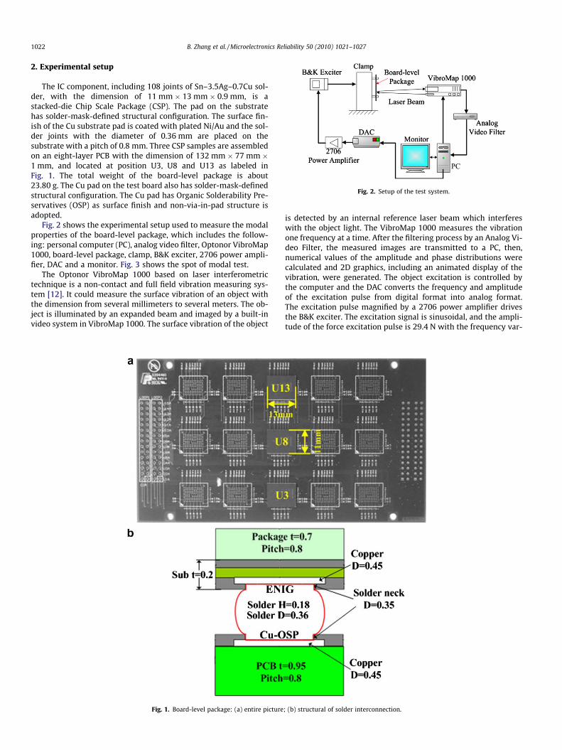
Fig. 2. Setup of the test system.
1022 B. Zhang et al. / Microelectronics Reliability 50 (2010) 1021–1027
2. Experimental setup
The IC component, including 108 joints of Sn–3.5Ag–0.7Cu sol-der, with the dimension of 11 mm � 13 mm � 0.9 mm, is astacked-die Chip Scale Package (CSP). The pad on the substratehas solder-mask-defined structural configuration. The surface fin-ish of the Cu substrate pad is coated with plated Ni/Au and the sol-der joints with the diameter of 0.36 mm are placed on thesubstrate with a pitch of 0.8 mm. Three CSP samples are assembledon an eight-layer PCB with the dimension of 132 mm � 77 mm �1 mm, and located at position U3, U8 and U13 as labeled inFig. 1. The total weight of the board-level package is about23.80 g. The Cu pad on the test board also has solder-mask-definedstructural configuration. The Cu pad has Organic Solderability Pre-servatives (OSP) as surface finish and non-via-in-pad structure isadopted.
Fig. 2 shows the experimental setup used to measure the modalproperties of the board-level package, which includes the follow-ing: personal computer (PC), analog video filter, Optonor VibroMap1000, board-level package, clamp, B&K exciter, 2706 power ampli-fier, DAC and a monitor. Fig. 3 shows the spot of modal test.
The Optonor VibroMap 1000 based on laser interferometrictechnique is a non-contact and full field vibration measuring sys-tem [12]. It could measure the surface vibration of an object withthe dimension from several millimeters to several meters. The ob-ject is illuminated by an expanded beam and imaged by a built-invideo system in VibroMap 1000. The surface vibration of the object
Fig. 1. Board-level package: (a) entire picture
is detected by an internal reference laser beam which interfereswith the object light. The VibroMap 1000 measures the vibrationone frequency at a time. After the filtering process by an Analog Vi-deo Filter, the measured images are transmitted to a PC, then,numerical values of the amplitude and phase distributions werecalculated and 2D graphics, including an animated display of thevibration, were generated. The object excitation is controlled bythe computer and the DAC converts the frequency and amplitudeof the excitation pulse from digital format into analog format.The excitation pulse magnified by a 2706 power amplifier drivesthe B&K exciter. The excitation signal is sinusoidal, and the ampli-tude of the force excitation pulse is 29.4 N with the frequency var-
; (b) structural of solder interconnection.
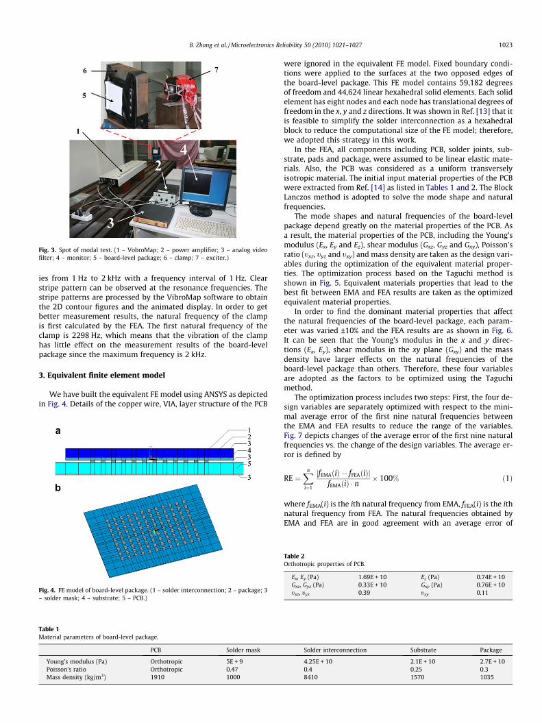
Fig. 3. Spot of modal test. (1 – VobroMap; 2 – power amplifier; 3 – analog videofilter; 4 – monitor; 5 – board-level package; 6 – clamp; 7 – exciter.)
B. Zhang et al. / Microelectronics Reliability 50 (2010) 1021–1027 1023
ies from 1 Hz to 2 kHz with a frequency interval of 1 Hz. Clearstripe pattern can be observed at the resonance frequencies. Thestripe patterns are processed by the VibroMap software to obtainthe 2D contour figures and the animated display. In order to getbetter measurement results, the natural frequency of the clampis first calculated by the FEA. The first natural frequency of theclamp is 2298 Hz, which means that the vibration of the clamphas little effect on the measurement results of the board-levelpackage since the maximum frequency is 2 kHz.
3. Equivalent finite element model
We have built the equivalent FE model using ANSYS as depictedin Fig. 4. Details of the copper wire, VIA, layer structure of the PCB
Fig. 4. FE model of board-level package. (1 – solder interconnection; 2 – package; 3– solder mask; 4 – substrate; 5 – PCB.)
Table 1Material parameters of board-level package.
PCB Solder mask
Young’s modulus (Pa) Orthotropic 5E + 9Poisson’s ratio Orthotropic 0.47Mass density (kg/m3) 1910 1000
were ignored in the equivalent FE model. Fixed boundary condi-tions were applied to the surfaces at the two opposed edges ofthe board-level package. This FE model contains 59,182 degreesof freedom and 44,624 linear hexahedral solid elements. Each solidelement has eight nodes and each node has translational degrees offreedom in the x, y and z directions. It was shown in Ref. [13] that itis feasible to simplify the solder interconnection as a hexahedralblock to reduce the computational size of the FE model; therefore,we adopted this strategy in this work.
In the FEA, all components including PCB, solder joints, sub-strate, pads and package, were assumed to be linear elastic mate-rials. Also, the PCB was considered as a uniform transverselyisotropic material. The initial input material properties of the PCBwere extracted from Ref. [14] as listed in Tables 1 and 2. The BlockLanczos method is adopted to solve the mode shape and naturalfrequencies.
The mode shapes and natural frequencies of the board-levelpackage depend greatly on the material properties of the PCB. Asa result, the material properties of the PCB, including the Young’smodulus (Ex, Ey and Ez), shear modulus (Gxz, Gyz and Gxy), Poisson’sratio (txz, tyz and txy) and mass density are taken as the design vari-ables during the optimization of the equivalent material proper-ties. The optimization process based on the Taguchi method isshown in Fig. 5. Equivalent materials properties that lead to thebest fit between EMA and FEA results are taken as the optimizedequivalent material properties.
In order to find the dominant material properties that affectthe natural frequencies of the board-level package, each param-eter was varied ±10% and the FEA results are as shown in Fig. 6.It can be seen that the Young’s modulus in the x and y direc-tions (Ex, Ey), shear modulus in the xy plane (Gxy) and the massdensity have larger effects on the natural frequencies of theboard-level package than others. Therefore, these four variablesare adopted as the factors to be optimized using the Taguchimethod.
The optimization process includes two steps: First, the four de-sign variables are separately optimized with respect to the mini-mal average error of the first nine natural frequencies betweenthe EMA and FEA results to reduce the range of the variables.Fig. 7 depicts changes of the average error of the first nine naturalfrequencies vs. the change of the design variables. The average er-ror is defined by
RE ¼Xn
i¼1
jfEMAðiÞ � fFEAðiÞjfEMAðiÞ � n
� 100% ð1Þ
where fEMA(i) is the ith natural frequency from EMA, fFEA(i) is the ithnatural frequency from FEA. The natural frequencies obtained byEMA and FEA are in good agreement with an average error of
Solder interconnection Substrate Package
4.25E + 10 2.1E + 10 2.7E + 100.4 0.25 0.38410 1570 1035
Table 2Orthotropic properties of PCB.
Ex, Ey (Pa) 1.69E + 10 Ez (Pa) 0.74E + 10Gxz, Gyz (Pa) 0.33E + 10 Gxy (Pa) 0.76E + 10txz, tyz 0.39 txy 0.11
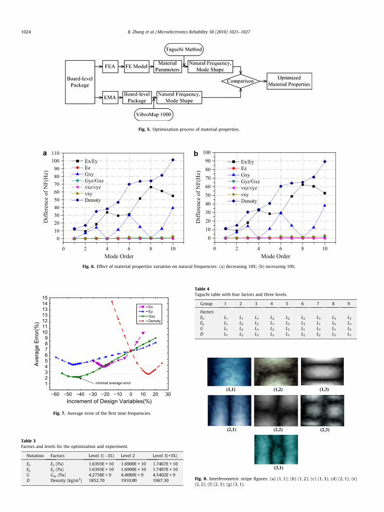
Fig. 5. Optimization process of material properties.
Fig. 6. Effect of material properties variation on natural frequencies: (a) decreasing 10%; (b) increasing 10%.
−60 −50 −40 −30 −20 −10 0 10 20 30
123456789
101112
1313
1415
Increment of Design Variables(%)
Aver
age
Erro
r(%)
ExEyGxyDensity
minimal average error
Fig. 7. Average error of the first nine frequencies.
Table 3Factors and levels for the optimization and experiment.
Notation Factors Level 1(�3%) Level 2 Level 3(+3%)
Ex Ex (Pa) 1.6393E + 10 1.6900E + 10 1.7407E + 10Ey Ey (Pa) 1.6393E + 10 1.6900E + 10 1.7407E + 10G Gxy (Pa) 4.2758E + 9 4.4080E + 9 4.5402E + 9D Density (kg/m3) 1852.70 1910.00 1967.30
Table 4Taguchi table with four factors and three levels.
Group 1 2 3 4 5 6 7 8 9
FactorsEx L1 L1 L1 L2 L2 L2 L3 L3 L3
Ey L1 L2 L3 L1 L2 L3 L1 L2 L3
G L1 L2 L3 L2 L3 L1 L3 L1 L2
D L1 L2 L3 L3 L1 L2 L2 L3 L1
Fig. 8. Interferometric stripe figures: (a) (1, 1); (b) (1, 2); (c) (1, 3); (d) (2, 1); (e)(2, 2); (f) (2, 3); (g) (3, 1).
1024 B. Zhang et al. / Microelectronics Reliability 50 (2010) 1021–1027
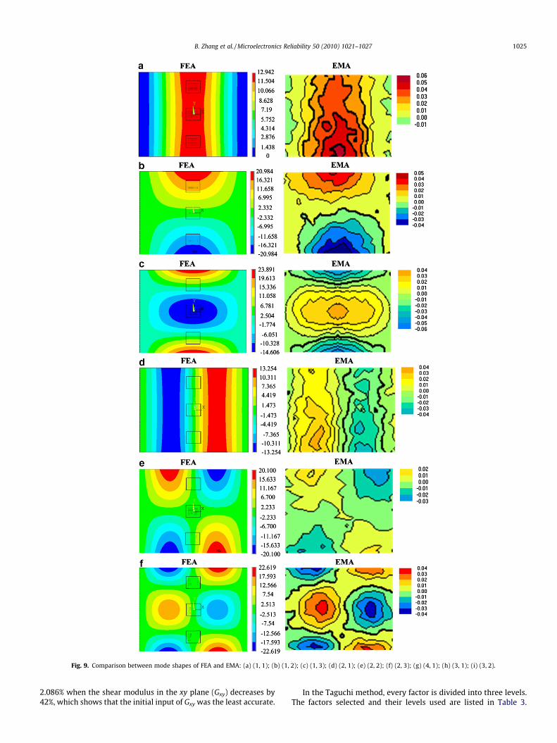
Fig. 9. Comparison between mode shapes of FEA and EMA: (a) (1, 1); (b) (1, 2); (c) (1, 3); (d) (2, 1); (e) (2, 2); (f) (2, 3); (g) (4, 1); (h) (3, 1); (i) (3, 2).
B. Zhang et al. / Microelectronics Reliability 50 (2010) 1021–1027 1025
2.086% when the shear modulus in the xy plane (Gxy) decreases by42%, which shows that the initial input of Gxy was the least accurate.
In the Taguchi method, every factor is divided into three levels.The factors selected and their levels used are listed in Table 3.
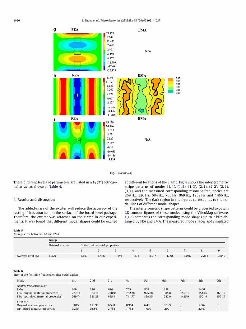
Fig. 9 (continued)
1026 B. Zhang et al. / Microelectronics Reliability 50 (2010) 1021–1027
These different levels of parameters are listed in a L9 (34) orthogo-nal array, as shown in Table 4.
4. Results and discussion
The added-mass of the exciter will reduce the accuracy of thetesting if it is attached on the surface of the board-level package.Therefore, the exciter was attached on the clamp in our experi-ments. It was found that different modal shapes could be excited
Table 5Average error between FEA and EMA.
Group
Original material Optimized material properties
1 2 3
Average error (%) 6.320 2.153 1.476 1.456
Table 6Error of the first nine frequencies after optimization.
Mode 1st 2nd 3rd
Natural frequencies (Hz)EMA 269 326 684FEA (original material properties) 277.11 364.11 728.94FEA (optimized material properties) 269.74 328.23 665.3
Error (%)Original material properties 3.015 11.690 6.570Optimized material properties 0.275 0.684 2.734
at different locations of the clamp. Fig. 8 shows the interferometricstripe patterns of modes (1, 1), (1, 2), (1, 3), (2, 1), (2, 2), (2, 3),(3, 1), and the measured corresponding resonant frequencies are269 Hz, 326 Hz, 684 Hz, 755 Hz, 869 Hz, 1258 Hz and 1466 Hz,respectively. The dark region in the figures corresponds to the no-dal lines of different modal shapes.
The interferometric stripe patterns could be processed to obtain2D contour figures of these modes using the VibroMap software.Fig. 9 compares the corresponding mode shapes up to 2 kHz ob-tained by FEA and EMA. The measured mode shapes and simulated
4 5 6 7 8 9
1.871 3.215 1.998 3.086 2.214 3.840
4th 5th 6th 7th 8th 9th
755 869 1258 / 1466 /762.28 925.28 1385.8 1501.1 1544.6 1681.5741.77 859.45 1242.9 1435.9 1501.9 1591.9
0.964 6.476 10.159 / 5.362 /1.752 1.099 1.200 / 2.449 /
B. Zhang et al. / Microelectronics Reliability 50 (2010) 1021–1027 1027
mode shapes using the optimized equivalent material propertiesare in good agreement.
We noticed certain degree of asymmetry in the measured 1stand 4th mode shapes, which was due to the nonuniform clampingat different locations of the board-level package. The 7th and 9thorder modes could not be excited maybe due to the setup designused in our experiments. Table 5 shows the average error of thefirst nine natural frequencies between EMA and FEA. It can be seenthat Group 3 reduces the average error from 6.32% to 1.456% com-pared with the initial input material properties. Table 6 lists somenatural frequencies and the errors between FEA and EMA resultsbefore and after the optimization. The natural frequencies ob-tained by FEA and EMA are in good agreement with a global errorless than 2%, while the error of the first natural frequency is lessthan 0.3%. Therefore, the third group material parameter in Table5 is adopted as the optimized equivalent material properties tobe used for the FEA of dynamic response of the board-levelpackage.
5. Conclusion
A laser-based interferometric technique has been used in thisinvestigation to measure the modal parameters of the board-levelpackage. The 132 mm � 72 mm � 1 mm board-level packagemounted with three 13 mm � 11 mm chip scale packages at theU3, U8 and U13 locations has been modeled using ANSYS. Theequivalent material properties of the PCB have been obtainedbased on the minimization of the global error between EMA andFEA results. These optimized equivalent material properties canbe used as input for the FEA in the future to study the dynamic re-sponse of the board-level package and the solder interconnections.
Acknowledgements
This work was supported in part by Natural Science Foundationof China under Grant 50905118 and 50805097, National High-tech
Research and Development Program (863 Program) Grant2006AA4Z334.
References
[1] Yeh Chang-Lin, Tsai Tsung-Yueh, Lai Yi-Shao. Transient analysis of dropresponses of board-level electronic packages using response spectraincorporated with modal superposition. Microelectron Reliab 2007;47(12):2188–96.
[2] Yeh Chang-Lin, Lai Yi-Shao. Support excitation scheme for transient analysis ofJEDEC board-level drop test. Microelectron Reliab 2006;46(2–4):626–36.
[3] Yeh Chang-Lin, Lai Yi-Shao, Kao Chin-Li. Evaluation of board-level reliability ofelectronic packages under consecutive drops. Microelectron Reliab2006;46(7):1172–82.
[4] Zhu Li-Ping, Marcinkiewicz Walt. Drop impact reliability analysis of CSPpackages at board and product levels through modeling approaches. IEEE TransCompon Pack Technol 2005;28(3):449–56.
[5] Shin Dong-Kil, Lee Duk-Yong, Ahn Eun-Chul, Kim Tae-Hun, Cho Tae-Je.Development of multi stack package with high drop reliability byexperimental and numerical methods. In: Proceedings – IEEE 56th electroniccomponents and technology conference; 2006. p. 377–82.
[6] Luan Jing-En, Tee Tong-Yan, Pek Eric, Lim Chwee-Teck, Zhong Zhao-Wei, ZhouJiang. Advanced numerical and experimental techniques for analysis ofdynamic responses and solder joint reliability during drop impact. IEEETrans Compon Pack Technol 2006;29(3):449–56.
[7] Luan Jing-en, Tee Tong-Yan, Pek Eric, Lim Chwee-Teck, Zhong Zhao-Wei.Dynamic responses and solder joint reliability under board level drop test.Microelectron Reliab 2007;47(2–3):450–60.
[8] Tee Tong-Yan, Ng Hun-Shen, Lim Chwee-Teck, Pek Eric, Zhong Zhao-Wei.Impact life prediction modeling of TFBGA packages under board level drop test.Microelectron Reliab 2004;44(7):1131–42.
[9] Chong DYR, Che FX, Pang John HL, Ng Kellin, Tan Jane YN, Low Patrick TH. Dropimpact reliability testing for lead-free and lead-based soldered IC packages.Microelectron Reliab 2006;46(7):1160–71.
[10] Lee Ying-Chih, Wang Bor-Tsuen, Lai Yi-Shao, Yeh Chang-Lin, Chen Rong-Sheng.Finite element model verification for packaged printed circuit board byexperimental modal analysis. Microelectron Reliab 2008;48(11–12):1837–46.
[11] Zhang Bo, Ding Han, Sheng Xin-Jun. Modal analysis of board-level electronicpackage. Microelectron Eng 2008;85(3):610–20.
[12] Optonor VibroMap 1000 user guide.[13] Ranouta Amarinder Singh, Fan XueJun, Han Qiang. Shock performance study of
solder joints in wafer level packages. In: International conference on electronicpackaging technology & high density packaging; 2009. p. 1266–76.
[14] Lall Pradeep, Islam Mohd-Nokibul, Singh Naveen, Suhling Jeffrey C, DarveauxRobert. Model for BGA and CSP reliability in automotive underhoodapplications. IEEE Trans Compon Pack Technol 2004;27(3):585–93.