Embed Size (px)
Citation preview

MODELING OF CALIBRATION CIRCUIT FOR
PARTIAL DISCHARGE MEASUREMENT
ADITYA KUMAR GUPTA (109EE0271)
SACHET RAY (109EE0181)
Department of Electrical Engineering National Institute of Technology Rourkela

MODELING OF CALIBRATION CIRCUIT FOR
PARTIAL DISCHARGE MEASUREMENT
A Thesis submitted in partial fulfillment of the requirements for the degree of
Bachelor of Technology in “Electrical Engineering”
By
ADITYA KUMAR GUPTA (109EE0271)
SACHET RAY (109EE0181)
Under guidance of
Prof. SUBRATA KARMAKAR
Department of Electrical Engineering National Institute of Technology
Rourkela-769008 (ODISHA) May-2013

i | P a g e
DEPARTMENT OF ELECTRICAL ENGINEERING
NATIONAL INSTITUTE OF TECHNOLOGY, ROURKELA
ODISHA, INDIA-769008
CERTIFICATE
This is to certify that the thesis entitled “Modelling of Calibration circuit for Partial
Discharge Measurement”, submitted by Aditya Kumar Gupta (Roll. No. 109EE0271)
and Sachet Ray (Roll. No. 109EE0181) in partial fulfillment of the requirements for the
award of Bachelor of Technology in Electrical Engineering during session 2012-2013 at
National Institute of Technology, Rourkela. A bonafide record of research work carried out
by them under my supervision and guidance.
The candidates have fulfilled all the prescribed requirements.
The Thesis which is based on candidates’ own work, have not submitted elsewhere for a
degree/diploma.
In my opinion, the thesis is of standard required for the award of a bachelor of technology
degree in Electrical Engineering.
Place: Rourkela Dept. of Electrical Engineering Prof. Subrata Karmakar National institute of Technology Assistant Professor Rourkela-769008

ii | P a g e
ACKNOWLEDGEMENTS On the submission of our thesis entitled “Modelling of Calibration Circuit for Partial
Discharge Measurement” we would like to extend our gratitude & our sincere thanks to our
supervisor Dr. Subrata Karmakar, Asst. Professor, Department of Electrical Engineering
for his constant motivation and support during the course of our work in the last one year. We
truly appreciate and value his esteemed guidance and encouragement from the beginning to
the end of this thesis. He not only served as our supervisor but also encouraged and
challenged us throughout the academic program. He guided us through the dissertation
process, never accepting any less than our best efforts. His reliable and incredible support
throughout our research work and his technical knowledge has led us through many problems
easily. We thank him for help and profiting us by his skill, support and valuable time and
criticisms, without which this project would not have been possible.
At last but not least, we would like to thank the staff of Electrical engineering
department for constant support and providing place to work during project period. We would
also like to extend our gratitude to our friends who are with us during thick and thin.
Aditya Kumar Gupta
B. Tech (Electrical Engineering)
Sachet Ray
B. Tech (Electrical Engineering)

iii | P a g e
Our beloved Parents
Dedicated to

iv | P a g e
ABSTRACT Most of the high voltage equipment suffers from failure due to internal faults. The type of
fault caused due to insulation failure as a consequence of local electrical stress concentration
in the insulation, whether gas, solid or liquid is very widely prevalent. This is called as partial
discharge. So, partial discharge detection is highly important for an early detection of
insulation failure. In this study, the simulation of partial discharge has been carried out with
consideration of a cylindrical void inside an epoxy resin. The PD characteristic is studied by
applying different high voltages across the insulation, which is necessary for designing of a
calibration circuit. A calibration circuit has been modelled in SIMULINK for generation of
PD pulses of known charge magnitude. The calibrator was connected across the test object
and the pulses were detected via detector. A physical model of calibrator was made and
output calibrating pulses were observed at Digital Storage Oscilloscope.

v | P a g e
Abstract iv
CONTENTS
Contents v
List of Figures vii
List of Tables ix
Abbreviations x
Chapter 1: Introduction 02
1.1 Introduction 02
1.2 Literature Review 02
1.3 Motivation and Objective of Thesis 03
1.4 Organization of Thesis 04
Chapter 2: Basic Concepts of Partial Discharge 07
2.1 Partial Discharge 07
2.2 Necessity of Detection of Partial Discharge 07
2.3 Classification of Partial Discharge 08
2.4 Effect of Partial Discharge on Insulating System 10
2.5 Partial Discharge Detection Methods 10
2.6 Role of Apparent Charge in Partial Discharge Measurement 10
Chapter-3: Modelling Of Partial Discharge Inside Solid Insulation 13
3.1 Selection of Void Parameters 13
3.2 Partial Discharge Measurement System 13
3.3 Electrical Circuit for PD Measurement 14
3.4 Simulink Model Description for Detection of Partial Discharge 15
3.5 Program to count Number of PD Pulses for One Cycle 17
Chapter-4: Analysis and Simulation of Calibrator 19
4.1 Apparent Charge 19
4.2 Calibration of PD Measuring Circuit 20
4.3 Pulse Shape Parameter 22
4.4 Calibrator Circuit Model 23
4.5 Circuit Model of Calibrator with Test Object 24

vi | P a g e
Chapter-5: Practical Implementation of Proposed Work Done 28
5.1 Introduction 28
5.2 IC555 Timer 29
5.3 Series RC Circuit 30
5.4 Switching Capacitor 31
5.5 Output Resistor 32
5.6 Complete Model of Calibrator Circuit 32
Chapter-6: Result and Discursions 34
6.1 Results for Partial Discharge Pulse Generation 34
6.2 Simulation Result of Calibrator and Overall Circuit 36
6.3 Result for Physical Calibrator Model 39
Chapter-7: Conclusion and Future Work 42
7.1 Conclusion 42
7.2 Future Work 42
References 43

vii | P a g e
LIST OF FIGURES
Fig. No. Name of the Figure Page No.
2.1 Various Types of Partial Discharge Occurring in Insulator 09
3.1 Void Model of the Epoxy Resin Insulator 13
3.2 Electrical Circuit Model for Partial Discharge Measurement 14
3.3 Simulink Model for Partial Discharge Detection 16
3.4 PD Pulse Counter Subsystem Circuit 16
4.1 Voltages across Test Object 19
4.2 PD Pulse Generator 22
4.3 PD Calibrator Circuit 24
4.4 PD Calibrator Circuit Connected Across Test Object 25
4.5 Calibrator Subsystem Circuit 25
4.6 Pulse Generator Subsystem Circuit 26
4.7 Controller Subsystem Circuit 26
5.1 PD Calibrator Circuit Diagram 28
5.2 IC555 Pin Diagram 29
5.3 IC555 as Astable Multi-Vibrator 30
5.4 Series RC Circuit of PD Calibrator 31
5.5 Parallel Set of Switching Capacitors 31
5.6 Output Resistor of PD Calibrator 32
5.7 Photograph of PD Calibrator Circuit Model 32
6.1 The Observed PD Pulse at 5 KV 34
6.2 The Observed PD Pulse at 10 KV 34
6.3 The Observed PD Pulse at 15 KV 35
6.4 Bar Graph showing Number of PD Pulses with Phase Angle 36
6.5 Pulse Voltage Source Output 36

viii | P a g e
6.6 Output of Pulse Generator 36
6.7 5 pC Charge Level by Choice 1 37
6.8 10 pC Charge Level by Choice 2 37
6.9 50 pC Charge Level by Choice 3 37
6.10 100 pC Charge Level by Choice 4 37
6.11 500 pC Charge Level by Choice 5 38
6.12 Output Pulses by Calibrator 38
6.13 Output Pulses from Detector Circuit 38
6.14 A Detector Circuit Output Pulse Expanded along time axis 38
6.15 Output Pulses from Series RC Circuit 39
6.16 Output Waveform from 4.7pF Capacitor 39
6.17 Output Waveform from 12pF Capacitor 40
6.18 Output Waveform from 56pF Capacitor 40
6.19 Input and Output Waveforms 40

ix | P a g e
LIST OF TABLES
Table No. Name of the Table Page No.
3.1 Parameter Used For PD Simulation 15
4.1 Pulse Shape Parameters 23
4.2 Pulse Shape Parameters for Simulation 23
4.3 Switching Capacitor Used in Simulation 23
4.4 Measuring Circuit Parameters 24
4.5 Pulse Generator Parameters for Simulation 26
5.1 Parameters of Elements Used with IC555 29
5.2 Resistor & Capacitor Values Used in IC555 30
5.3 Values of Switching Capacitors 31
6.1 Number of PD Pulse Appearing for Phase Range of 45° 35

x | P a g e
LIST OF ABBREVIATIONS IEC standard International Electro Technical Commission PD Partial Discharge HV High Voltage MI Measuring Instrument PRPD Phase Resolved Partial Discharge NEMA National Electrical Manufacturers Association
IC Integrated Circuit
DUT Device Under Test
DSO Digital Storage Oscilloscope

1 | P a g e
CHAPTER1
INTRODUCTION Introduction
Literature review Motivation and Objective of the Thesis
Organization of the Thesis

2 | P a g e
1.1 INTRODUCTION
With the rapid growth of electrical energy consumption over the years, increasingly in the
developed countries like India, has led to the development of many high voltage transmission
and distribution systems and that too with increasing levels of sophistication. But, as is the
case with almost all the equipment, however perfect their initial state is, continuous use of the
instrument inevitably leads to the failure of insulation. Heat and vibration, thermal cycles and
the presence of high electric stress are major culprits responsible for degradation of integrity
of the dielectric system. Thus the major problem associated with increasing levels of
complexity and efficiency is reliability and lifetime of the instrument [1].
So, as is obvious, it becomes quite pertinent to measure the quality of the insulation at
periodic intervals. Partial discharge (PD) measurement is one of the many methods used to
determine the quality and lifetime of insulation. Partial discharge is defined as localized
electrical discharge that only partially bridges the insulation between electrodes. It is known
that no type of insulation is completely pure and does not contain any impurities. Some form
of impurity or air bubbles is always present during the manufacturing process [2]. The
presence of these impurities weakens the insulation and is responsible for occurrence of
partial discharge. Thus partial discharge measurement becomes an important process to
determine the state of insulation [3].
1.2 LITERATURE REVIEW
Although high voltage technology for electrical power generation and transmission
systems, was introduced during the earlier parts of last century, by then partial discharge had
been recognized as a harmful source for insulation ageing in the high voltage apparatus. With
passing time, many techniques have been developed for detection, measurement and behavior
study of PDs in insulation. The very beginning of partial discharge recognition dates back to
the year 1777, in which Lichtenberg reported on novel results of experimental studies during
a session of Royal Society in Gottingen. Since then, many authors have presented their work
about the detection and measurement of PDs, as well as study the characteristic of PDs. The
very beginning of partial discharge recognition dates back to the year 1777, in which
Lichtenberg reported on novel results of experimental studies during a session of Royal
Society in Gottingen. Although it was almost 100 years, before it could be clarified that
Lichtenberg dust figures manifest electrical discharge channels on the surface of the
dielectrics [4].

3 | P a g e
With rapidly increasing HV transmission voltage level, a substantial improvement in
the insulating materials was required. So, the first facilities for electrical PD recognition were
introduced at the beginning of the last century, which helped in continuous improvement of
knowledge about PDs. With increasing knowledge about PD recognition, industrial PD
detectors were developed in the middle of the last century, which essentially paved the way
for further achievements in the field.
During the 1970’s, the measurement of PDs down to pC range was demanded due to
the introduction of extruded materials for the insulation of power cables as PDs of few pc
may lead to an inevitable breakdown of insulation. This enforced the development of
improved PD measuring systems, which were also capable of localization of PD sites in long
distance power cables [5]. Along with that, PD tests in compliance to IEC 60270 were
compulsorily applied for quality assurance checks of power transformers.
Since the 1970s, conventional analogue instruments have been increasingly
substituted by digital instruments which are more powerful and produce better results, to
satisfy the ever increasing technical and scientific interest in the stochastic nature of PDs. For
the first few years, multi-channel pulse height analyzers were used, which was later
substituted by computerized PD measuring systems capable of processing, acquisition and
phase-resolved visualization of very complex PD data. Now days, the digital PD
measurement technique is common practice in the laboratories all over the world.
1.3 MOTIVATION AND OBJECTIVE OF THESIS
PDs are generally caused due to imperfections in the insulation system which
inevitably leads to failure of high voltage equipment. The insulation of equipment plays a
major role in the lifetime of equipment. So, it is necessary for the insulation to be high quality
to maintain the efficiency. But it is nigh impossible to produce insulation materials, which are
completely free of impurities, PD detection is of paramount importance. The impurities
present are in the form of solid, liquid or gas. It is commonly noted that, during
manufacturing process of solid insulations, air bubbles are present which leads to weakening
of the insulation on application of high voltage [6].
Since it is practically impossible to quantify the PD that appears in the insulation
defect, a related electrical quantity called as apparent charge q, is used to quantify the PD
phenomenon. The apparent charge, q, is defined as the charge which when injected across the
Device Under Test (DUT) for a very short period of time in a specified test circuit, produces
the same result as the PD pulse itself [7]. The ratio of the input quantity to the instrument

4 | P a g e
reading, also known as scale factor is determined by means of a suitable calibrator in the test
circuit. To a great extent, the accuracy of the PD calibrator used in the circuit determines the
accuracy of the PD measurement.
The main objectives of the thesis are:
To find out PD activity inside the void enclosed with the solid insulation using
MATLAB based SIMULINK models for different input voltages.
To find out the
o Maximum PD magnitude variation with different applied voltage
o Number of PDs and other PD related parameters like PD distribution
o Frequency content of obtained PD pulse.
To design a MATLAB based SIMULINK model of calibrating circuit for partial
discharge detection.
To utilize the calibrating circuit to produce PDs.
To design a physical model of calibrator and observe the experimental results.
1.4 ORGANISATION OF THESIS
The thesis is categorized into five different chapters including the introduction.
Chapter 1: This chapter comprises of introduction, motivation & objective of the project along the literature review on partial discharge characteristics as well as the organization of the thesis.
Chapter 2: This chapter describes basic concepts of partial discharge i.e. the necessity and detection of partial discharge in high voltage power equipment and the role of
apparent charge for PD measurement.
Chapter 3: The mathematical modelling of partial discharge inside solid insulation is
discussed in this chapter. It includes the cylindrical void model present in the
solid insulation and its equivalent circuit model for measurement of PD pulses.
Chapter 4: This chapter describes the concepts of apparent charge and the method to
calibrate a PD measuring instrument. A MATLAB-SIMULINK model of
calibrator is made for different charge level. The model is also simulated across
test object.

5 | P a g e
Chapter 5: This chapter presents the physical model of calibrator circuit. It consists of
IC555 TIMER circuit, series RC circuit, a set of capacitors connected in parallel
and output resistor. Varying charge level is obtained by different capacitors.
Chapter 6: In this chapter the results of simulation of PD pulse generation, simulation of
calibrator circuit, simulation of calibrator circuit with test object and output
waveforms of physical model is presented.
Chapter 7: In this chapter the conclusion and future work has been discussed.

6 | P a g e
CHAPTER2
BASIC CONCEPTS OF PARTIAL DISCHARGE (PD)
Partial discharge
Necessity of Detection of Partial Discharge Classification of Partial Discharge
Effect of Partial Discharge on Insulating Systems Partial Discharge Detection Methods
Role of Apparent Charge in Partial Discharge Measurement

7 | P a g e
2.1 PARTIAL DISCHARGE
According to IEC 60270 (International Electro-technical Commission), Partial
Discharge is defined as: “localized electrical discharge, that only partially bridges the
insulation between conductors and which may or may not occur adjacent to a conductor.
Partial discharges are in general a consequence of local electrical stress concentration in the
insulation or on the surface of insulation. Generally, such discharges appear as pulses
having duration of much less than 1µs”. PD activity, in general, is observed in high voltage
power equipment like transformers, bushings and many others [8].
2.2 NECESSITY OF PARTIAL DISCHARGE DETECTION
PD usually occurs within voids, cracks, or in any inclusions within a solid dielectric,
at the conductor-dielectric interface within a solid dielectric, or in bubbles within a liquid
dielectric. As the PDs are only limited to a portion of the insulation, the discharges can only
partially bridge the distance between electrodes. Partial discharge (PD) can also occur along
the boundary between different insulating materials, also along the surface of solid insulating
materials if the surface tangential electric field is high enough to cause a breakdown along the
surface of the insulator [9]. This phenomenon is commonly manifested in overhead line
insulators, mainly on contaminated insulators during days of high humidity. This
phenomenon is also known as corona effect.
Most of insulators are in impure form due to presence of air bubbles which creates
voids within the insulating material. It is responsible for weakening of the insulating material
and appearance of PDs. The reason being, the dielectric constant of the void as compared to
its surrounding is less. So, it leads insulation failure in high voltage and high power
equipment. Although such type of discharges has very low magnitude, over a sufficient
period of time, it leads to degradation of the insulating material, which ultimately leads to the failure of the system. For this reason, PD detection and measurement is of utmost importance.

8 | P a g e
2.3 CLASSIFICATION OF PARTIAL DISCHARGE
Partial Discharge phenomenon can be divided into two categories [3]:
External Partial Discharge: External Partial discharge is defined as the partial
discharge occurring in ambient air, also normally known as corona discharge. This
type of discharges is usually reversible and thus generally considered as harmless.
Internal Partial Discharge: Partial discharges occurring due to imperfections in
insulating liquids and solid dielectrics as well as in compressed gas are defined as
internal partial discharges [10].
PD phenomenon can also be classified into the following types:
Corona Discharge: It takes place due to the non-uniformity of electric field on sharp
edges of conductor subjected to high voltage. The insulation used for such type of
discharge may be gas or air or liquid [11]. This type of discharges appears for a long
duration along the bare conductor. The Ozone formed due to the corona effect is
responsible for the degradation of the insulation material.
Surface Discharge: It takes place on interfaces of dielectric materials such as gas/solid
interface. This usually occurs in bushings, end of cable, any point on insulator
surface, between electrodes (high voltage terminal & ground). The existence of such
discharge depends on various factors such as:
o Permittivity of the dielectric materials used
o Voltage distribution between the conductors
o Properties of the insulating materials
Treeing Channel: At the sharp edges of an insulating material, high intensity fields are
produced, resulting in deterioration of the insulating material. This leads to a
continuous partial discharge, also known as Treeing Channel.
Cavity Discharge: This type of discharge usually occurs in solid or liquid insulating
materials. The cavity present is generally filled with gas or air. When the gas in the
cavity is over stressed, Cavity Discharge takes place.

9 | P a g e
(a) (b)
(c) (d)
FIGURE 2.1: Various Types Of Partial Discharge Occurring in the Insulator a) Corona or Gas
Discharge, b) Surface Discharge, c) Treeing Channel and d) Cavity Discharge

10 | P a g e
2.4 EFFECT OF PARTIAL DISCHARGE ON INSULATING SYSTEM
Once started, PD causes progressive deterioration of the insulating material,
eventually leading to electrical breakdown of the system. The effects of PD within high
voltage cables and equipment can be very serious. The collective effect of partial discharges
within solid dielectrics leads to treeing effect which causes the formation of numerous
partially conducting discharge channels. Repetitive discharges cause irreversible mechanical
and chemical deterioration of the insulating material. Damage is usually caused due to the
energy dissipation by high energy electrons or ions from the discharges, and liberation of
gases at high pressure due to chemical breakdown processes. The chemical transformation of
the dielectric is also responsible for increase in the electrical conductivity of the dielectric
material surrounding the voids, which lead to increase in the electrical stress in the unaffected
gap region, accelerating the breakdown process of the insulating material.
PD dissipates energy, generally in the form of heat, but sometimes in the form of
sound and light as well, for example the hissing and dim glowing around the overhead line
insulators. Heat energy dissipation may cause thermal degradation of the insulation, although
to a very small extent. For high voltage equipment, the reliability of the insulating material
can be confirmed by monitoring the PD activities. PD in high-voltage electrical equipment
should be monitored closely to ensure supply reliability and long-term operational
sustainability, along with early warning signals for inspection and maintenance.
2.5 PARTIAL DISCHARGE DETECTION METHODS
Many techniques are used for the detection of PD as well as its measurement on the basis of both electrical and non-electrical methods. The techniques which are popularly used for measurement of PDs are,
Chemical Detection Method
Acoustic Detection Method
Optical Detection Method
Electrical Detection Method
2.6 ROLE OF APPARANT CHARGE IN PD MEASUREMENT
Partial discharge is a type electrical discharge that can lead to serious problems in
high voltage equipment. The value of charge stored in the voids in the insulating material
cannot be directly measured as the PD sources are not accessible.. Thus, partial discharge
cannot be quantified by direct methods. To overcome this problem, an apparent charge

11 | P a g e
method is used for the measurement of the PD activity inside the solid insulation model.
Apparent charge is defined as the amount of charge which when injected across the terminals
of the Device Under Test (DUT) in a specified test circuit produces the same result on the
measuring instrument as does the PD current pulse itself. The apparent charge is usually in
Pico-coulombs. And in order to measure the apparent charge the measuring instrument needs
to be calibrated as the partial discharge is highly dependent upon the geometrical
configuration of the void location inside the solid insulation.

12 | P a g e
CHAPTER3
MODELLING OF PARTIAL DISCHARGE INSIDE SOLID INSULATION
Selection of Void Parameters
Partial Discharge Measurement System Electrical Circuit for Partial Discharge Measurement
Simulink Model Description for Detection of Partial Discharge

13 | P a g e
3.1 SELECTION OF VOID PARAMETER
The most important factor for partial discharge characteristics is void parameters.
Partial discharge characteristics changes accordingly, with the size of void. There are several
types of voids as such as cylindrical, cubical, rectangular, etc. So the main parameters which
are required for the analysis are height, length, breadth, diameter and volume of the void.
FIGURE 3.1: Void Model of the Epoxy Resin Insulator
The test object used is made up of epoxy resin and consists of three capacitors.
Among three capacitors, two are connected in series with parallel to the other. Where, Ca is
the capacitance of the healthy part of the test object, Cc is the capacitance of the void present
in the test object and Cb is the capacitance of the part of the test object leaving Ca and Cc [12].
3.2 PARTIAL DISCHARGE MEASUREMENT SYSTEM
The major components required for Partial Discharge Measurement are:
A coupling capacitor, when connected in series with the measuring system, due to its
low high impedance holds up the low level partial discharge at a particular applied
voltage for measurement of partial discharge. A higher level of partial discharge is
measured when coupling capacitor and measuring system is connected separately while
the measuring system is connected in series with the test objet.
A High voltage supply with low degree of background noise is provided as input
supply to the system.
50mm
20mm
50mm
5mm
5mm

14 | P a g e
High voltage connections having sufficiently low degree of background noise.
Rm, Lm, and Cm are taken as the input impedances for the measuring system. The
input impedance of the system determines the wave shape of the PD impulse.
The test object consists up of three capacitors: one connected in parallel with the
other two which are connected in series.
Cc represents the cylindrical void present inside the
Solid insulation.
Test object Cb represents the capacitance of the remaining series
insulation with void (Cc)
Ca represents the capacitance of the remaining
Discharge free insulation of the rest of the solid insulator
A measurement instrument is used across the detector circuit to measure the partial
discharge pulses produced due to presence of void inside the test object
PC software is used for characteristic study and analysis. 3.3 ELECTRICAL CIRCUIT MODEL FOR PD MEASUREMENT
FIGURE 3.2: Electrical Circuit Model for Partial Discharge Measurement
Fig.3.2 consists of three capacitors. Capacitor Cc represents capacitance of the void present in
the test object which is shown in Fig. 3.1. Capacitor Cb represents capacitance of the healthy
part connected in series with the void. Capacitor Ca represents capacitance of the healthy
part leaving Cc and Cb. When a high voltage supply is given to the circuit model then
discharge occurs. With this high voltage the void gets charged and breakdown starts [13]. A
measuring instrument is connected across the detector circuit in order to receive this pulse
High Voltage source
Ca
Z
Zm
Cc
Cb
Ck

15 | P a g e
from the test object through detector circuit. An epoxy resin insulator with dimensions
50mm, 50mm and 20mm is considered. In that insulator a cubical void is present. The void is
having radius of 5mm and height of 5mm. As the electrical circuit model consists of three
capacitors the value of those capacitors is to be found out. It is known that,
C = [(ε0εrA)/d] (1)
Where, C is the capacitance, with permittivity of free space and the relative permittivity and d
is the distance between the electrodes. Therefore,
Cc = (ε0A)𝑡𝑡
= 0.139×10⁻¹² F (2)
Cb = (ε0ε𝑟𝑟𝐴𝐴)𝑑𝑑−𝑡𝑡
= 0.162×10⁻¹²F (3)
Ca = (ε0ε𝑟𝑟A1)𝑑𝑑
= 3.752×10⁻¹² F (4)
The capacitances values of the three capacitors are calculated. This value is required for
measurement of partial discharge pulses.
When this circuit is energized by a high voltage AC source, a recurrent discharge occurs.
Voltage across the capacitance Cc is given by
𝑉𝑉𝑐𝑐 = 𝑉𝑉𝑎𝑎 × 𝐶𝐶𝑏𝑏/(𝐶𝐶𝑎𝑎 + 𝐶𝐶𝑏𝑏) (5)
The apparent charge measurable at the high voltage terminal and ground terminal can be
calculated from the following equation
𝑄𝑄 = 𝐶𝐶𝑏𝑏 × 𝑉𝑉𝑐𝑐 (6)
3.4 SIMULINK MODEL FOR DETECTION OF PARTIAL DISCHARGE
A simple equivalent capacitor circuit of model of the solid insulator is used in the MATLAB
SIMIULINK to evaluate the fundamental quantities of the PD pulse.
TABLE3.1: Parameters Used for PD Simulation Sl. no Parameter Symbol Value Dimension
1. Input Resistance Rin 1000 Ohm 2. Coupling Capacitor Ck 1000 µF 3. Permittivity ε0 8.85*10-12 F/m 4. Relative Permittivity εr 3.5 - 5. Resistance Rm 100 Ohm 6. Inductance Lm 0.6 mH 7. Capacitance Cm 0.1 µF

16 | P a g e
Here, an equivalent circuit of solid insulator having a cubical void is taken to evaluate
the partial discharge pulses. In this insulator the void is present at the center of the insulation
medium. The value of three capacitors shown in the electrical circuit model is calculated.
Here generally, (Ca>>Cc>>Cb). In this study the value of void model and other parameters are
calculated. The figure below shows the SIMULINK model which is used for the detection of
partial discharge which is shown in Fig. 3.3.
FIGURE 3.3: Simulink Model for Partial Discharge Detection
FIGURE 3.4: PD Pulse Counter Subsystem Circuit
Continuous
powergui
Vout
v+-V2
v+-V1
V discharge
simout
To Workspace
Scope2
Scope1
Rm
Rin
In1Out1
Out2
PD Pulse counter
Lm
-K-
Gain
Cm
Ck
Cc
Cb
Ca
AC Voltage Source
V discharge
V discharge
Vi
2Out2
1Out1
Scope1
Scope
Product
Edge Detector1
CountUp
Inc Cnt
Counter
Add
= 1e-00
>=1e-5
>= 0.5
>=0.5= -1e-00
<=-1e-5
1In1
V discharge

17 | P a g e
3.5 PROGRAM TO COUNT NUMBER OF PD PULSES FOR ONE CYCLE
PD pulse output was considered for one ac cycle i.e. for 0.02sec or 2𝜋𝜋 radians. The
number of PD pulses was counted by the PD Pulse Counter subsystem shown in figure 3.4.
An edge detector was used whose output becomes 1 as soon as it detects a rising edge of
input i.e. PD pulse waveform. The output of edge detector was fed to a pulse counter which
counts the PD pulses. This output values were taken to workspace. A program was composed
in MATLAB. A while loop and for loop were used which counts the number of PD pulses
appearing in each section of 45oor for time interval of 0.0025 sec for one ac cycle [14]. PD
pulses were counted for 5 KV and 10 KV, and the numbers were plotted in form of chart.

18 | P a g e
CHAPTER4
ANALYSIS AND SIMULATION OF CALIBRATOR Apparent Charge
Calibration of PD Measuring Circuit Pulse Shape Parameters
Calibrator Circuit Model Circuit Model of Calibrator with Test Object

19 | P a g e
4.1 APPARENT CHARGE Since actual PD, which appears inside the insulation defect, cannot be directly
measured, another related electrical quantity, the apparent charge qa, is used to quantify the
PD phenomenon. The ‘apparent charge’ of a PD pulse is the charge which, if injected within
a very short time across the terminals of the Device Under Test (DUT) in a specified test
circuit, would give the same reading on the measuring instrument as the PD current pulse
itself. PD tests are performed by applying, through a supply circuit, the high voltage to the
DUT and by measuring the apparent charge consequent to the PD event [15]. The
determination of the measuring system scale factor, that is the ratio of the input quantity to
the instrument indication, is performed by means of a suitable calibrator in the complete test
circuit, because the measuring system response depends on the test circuit configuration [16].
The calibration procedure consists in injecting across the DUT a current pulse of known
charge, generated by a PD calibrator, in absence of high voltage supply. The calibrator is
essentially composed of a step voltage generator and a series capacitor.
FIGURE 4.1: Voltages across Test Object
Where,
U1= Test voltage applied
U2= Voltage across PD source
U3= Voltage across Zm
Zm
Cb
Cc
U2
U3
U1
Ca

20 | P a g e
U3= U1×𝐶𝐶𝑎𝑎
(𝐶𝐶𝑎𝑎+𝐶𝐶𝐶𝐶) (7)
As Cm>>Ca,
U3×Cm = U1×Ca = qa = apparent charge (8)
It means that qa stored temporarily in virtual test object capacitance can be evaluated
by measuring transient voltage magnitude U3 across measuring capacitance Cm.
As Ca>>Cb,
Qa = U1×Ca = U2×Cb (9)
Qa = U2×Ca×𝐶𝐶𝑏𝑏𝐶𝐶𝑎𝑎
= qc×𝐶𝐶𝑏𝑏𝐶𝐶𝑎𝑎
(10)
As Cb/Cc<<1 thus the charge at test object terminals is only a small fraction of charge
created at PD site.
4.2 CALIBRATION OF PD MEASURING CIRCUIT
The quantitative assessment of the apparent charge transferred from the PD source to
the terminals of the test object is based on the approach of Gemant and Philippoff, often
referred to as a – b – c model due to the characteristic capacitances. Due to the series
connection of Cb and Cc , where the condition Cb / Cc<< 1 is always satisfied, the apparent
charge qa detectable at the test object terminals can be written as:
qa = qc × 𝐶𝐶𝑏𝑏𝐶𝐶𝑐𝑐
(11)
That means the measurable apparent charge qa is only a small fraction of the true
pulse charge qc created in the PD source. Consequently, the PD severity of HV apparatus
cannot be estimated on the basis of the apparent charge alone, because the ratio Cb / Cc is not
known at all. Therefore, knowledge rules for PD diagnosis have been established in the past
which are based on practical experiences gained from comprehensive PD studies in
laboratory and on-site [17]. Each PD event causes a reading Ri of the PD instrument which is
proportional to qa. To measure this quantity in terms of Pico Coulomb (pC) the Standard IEC
60270 specifies a calibration method which is based on the simulation of the internal charge

21 | P a g e
transfer between the PD source and the terminals of the HV apparatus by means of an
external adapted calibrator. Based on this calibration procedure the apparent charge of a PD
pulse is defined in IEC 60270 as: “that charge which, if injected within a very short time
between the terminals of the test object in a specified test circuit, would give the same
reading on the measuring instrument as the PD current pulse itself.” The PD calibrator is
generally equipped with a pulse generator connected in series with a calibrating capacitor. In
order to simulate the transient voltage across the PD defect the pulse generator creates
equidistant voltage steps of known magnitudes U0 [18]. If the value of the calibrating
capacitor C0 is substantially lower than the value of the virtual test object capacitance Ca, the
calibrating charge injected in the test object terminals, can simply be expressed by:
q0 =C0 × U0 = Ca × U1 (12)
If real PD events appear, the apparent charge is given by:
qa = Ca × U2 (13)
Introducing equation (12) in equation (13) the unknown value of Ca can be eliminated. Thus,
qa = q0 × ( U2 / U1 ) (14)
Because the transient voltages U1 and U2, which appear across the test object capacitance Ca,
cause the readings R0 and Ri, equation (14) can also be written as:
qa = q0 × ( Ri / R0 ) (15)
Where the ratio Ri / R0 represents the scale factor, Sf of the PD measuring circuit applied.
Thus a PD calibrator is equipped with a pulse generator in series with a calibrating capacitor
so that calibration pulses are produced which are repetitive charge of magnitude q0 [19]
Q0 = U0 × C0 (16)

22 | P a g e
FIGURE 4.2: PD Pulse Generator
Where,
U0 = Input step voltage
C0 = Calibrating generator capacitance
Um = Output voltage across Rm
In order to determine magnitude of calibrating charge, time dependent voltage Um(t)
appearing across Rm has to be integrated in order to determine the magnitude of calibrating
charge.
q0 = ∫ 𝑖𝑖𝐶𝐶(𝑡𝑡)𝑑𝑑𝑡𝑡 (17)
𝑞𝑞0 = 1𝑅𝑅𝐶𝐶
× ∫ 𝑖𝑖𝐶𝐶(𝑡𝑡)𝑑𝑑𝑡𝑡 (18)
4.3 PULSE SHAPE PARAMETERS
As the charge transfer from PD site to test terminals is finished in few nanoseconds.
Therefore step pulse generator should have an equivalent rise time, because charge transfer
by calibrating capacitor is governed by tr. The impact of step pulse shape on the uncertainty of
calibrating charge can be neglected by following conditions [20]:
U0 Um Rm
C0

23 | P a g e
TABLE 4.1: Pulse Shape Parameters
Sl. no. Parameters Conditions 1. Rise time Tr<60 ns 2. Time to steady state Ts<500 ns 3. Steady state duration Td>5µs 4. Overshoot Ud<0.1U0 5. Undershoot Ut<0.1U0
4.4 CALIBRATOR CIRCUIT MODEL
A PD calibrator is equipped with a pulse generator in series with a calibrating
capacitor. Generator produces step voltage pulses of desired magnitude which produces PD
pulses of required charge levels (in pC).
In MATLAB-SIMULINK environment, the Pulse voltage source is used with following parameters:
TABLE 4.2: Pulse Shape Parameters for Simulation
Sl. no. Parameters Values 1. Initial value, V1 0V 2. Pulse value, V2 9V 3. Pulse delay time, td 0 sec 4. Pulse rise time, tr 10−9𝑠𝑠𝑠𝑠𝑐𝑐 5. Pulse fall time, tf 10−9𝑠𝑠𝑠𝑠𝑐𝑐 6. Pulse width, pw 4 × 10⁻⁴𝑠𝑠𝑠𝑠𝑐𝑐 7. Pulse period, per 16 × 10−4𝑠𝑠𝑠𝑠𝑐𝑐
Pulse Generator is in series with parallel set of switching capacitors. Capacitors were
connected in parallel and the variable charge level was obtained by switching to different
capacitors. The switching action was done by switches which were controlled by a controller.
An input choice is given to controller and the required capacitor was switched.
The various parameters used for calibrator circuit:
TABLE 4.3: Switching Capacitors Used in Simulation
Sl. No. Parameter Values Dimensions 1. Capacitor 1 0.56 pF 2. Capacitor 2 1.11 pF 3. Capacitor 3 5.56 pF 4. Capacitor 4 11.11 pF 5. Capacitor 5 111.11 pF 6. Resistor 500 kΩ

24 | P a g e
FIGURE 4.3: PD Calibrator Circuit
4.5 CIRCUIT MODEL OF CALIBRATOR WITH TEST OBJECT
Now, the calibrator was connected across the test object and the output pulses were
observed through measuring circuit. The measuring circuit consists of parallel RC circuit. A
coupling capacitor was connected in series to the measuring circuit. This measuring circuit in
series with coupling capacitor was connected across the test object.
The parameter values for measuring circuit were as:
TABLE 4.4: Measuring Circuit Parameters
Sl. no. Parameter Symbol Value 1. Measuring Capacitor Cm 1 µF 2. Measuring resistor Rm 100 Ω
As the capacitance of the test object and its voids are in Pico-coulomb range and the
capacitors used in calibrators are also in Pico-coulombs. Hence, before connecting to the test
object, the calibrator is connected to a buffer amplifier to prevent loading effects.
Input choices were given to get the desired Pico-coulomb level charges. The output
pulses were observed through measuring circuit.
INPUT CHOICES:1 = 5pC2 = 10 pC3 = 50 pC4 = 100 pC5 = 1000 pC
+V -
Voltage Sensor3
+V -
Voltage Sensor1
PS
Switch5
PS
Switch4
PS
Switch3
PS
Switch2
PS
Switch1
f(x)=0
SolverConfiguration2
f(x)=0
SolverConfiguration1
PSS
Simulink-PSConverter5
PSS
Simulink-PSConverter4
PSS
Simulink-PSConverter3
PSS
Simulink-PSConverter1
PSS
Simulink-PSConverter
+-
Resistor
Pulse Voltage Source1
PS S
PS-SimulinkConverter4
PS S
PS-SimulinkConverter3
PS S
PS-SimulinkConverter1
INPUTS:1,2,3,4,5
INPUT VOLTAGE1
INPUT VOLTAGE
Electrical Reference1
+ -
Capacitor5
+ -
Capacitor4
+ -
Capacitor3
+ -
Capacitor2
+ -
Capacitor1
Controller Input
Controller Output1
Controller Output2
Controller Output3
Controller Output4
Controller Output5
CONTROLLER

25 | P a g e
The overall circuit is as:
FIGURE 4.4: PD Calibrator Circuit Connected across Test Object
The calibrator circuit consisted of Pulse generator and a set of switching capacitors which
were switched through inputs given to controller. The calibrator subsystem is as shown:
FIGURE 4.5: Calibrator Subsystem Circuit
INPUT CHOICES:1 = 5pC2 = 10 pC3 = 50 pC4 = 100 pC5 = 500 pC
+V -
Voltage Sensor2
+-
Rm
+ -
Resistor1
PS S
PS-SimulinkConverter6
PS S
PS-SimulinkConverter2
+
-
Op-Amp
OUTPUT CURRENT PULSE
INPUTS:1,2,3,4,5
INPUT VOLTAGE
DETECTOR VOLTAGE
+I
-
Current Sensor1
+-
Cm
+-
Ck
+-
Cc
+-
Cb
+-
Ca
CALIBRATOR VOLTAGE
CALIBRATOR CURRENT PULSE
Out1
Out2
Pulse Generator Output
Conn1
Conn2
Conn3
CALIBRATOR
3Pulse Generator Output
2Out2
1Out1
3Conn3
2Conn2
1Conn1
+V -
Voltage Sensor1
PS
Switch5
PS
Switch4
PS
Switch3
PS
Switch2
PS
Switch1
f(x)=0
SolverConfiguration3
f(x)=0
SolverConfiguration1
PSS
Simulink-PSConverter5
PSS
Simulink-PSConverter4
PSS
Simulink-PSConverter3
PSS
Simulink-PSConverter1
PSS
Simulink-PSConverter
+-
Resistor
Pulse Generator Output
Conn1
Conn2
Pulse Generator
PS S
PS-SimulinkConverter5
PS S
PS-SimulinkConverter3
PS S
PS-SimulinkConverter1
Electrical Reference1
+I
-
Current Sensor
+ -
Capacitor5
+ -
Capacitor4
+ -
Capacitor3
+ -
Capacitor2
+ -
Capacitor1
Controller Input
Controller Output1
Controller Output2
Controller Output3
Controller Output4
Controller Output5
CONTROLLER

26 | P a g e
The Pulse Generator consists of a pulse voltage source, whose output is supposed to be taken
from an IC 555 timer circuit. The output pulse of the timer is then fed to a series RC circuit.
The series RC circuit is used to achieve the desired rise time (<60 ns), fall time and pulse
duration (>5µs).
The various parameters used for PD generator in simulation are:
TABLE 4.5: Pulse Generator Parameters Used for Simulation
Sl. No. Parameter Values Unit 1. Pulse Voltage Source 0-9 V 1. Resistor 1 Ω 2. Resistor 1 50 Ω 3. Capacitor 1 µF
The Pulse Generator subsystem is shown as:
FIGURE 4.6: Pulse Generator Subsystem Circuit
FIGURE 4.7: Controller Subsystem Circuit
1Pulse Generator Output
2Conn2
1Conn1
+V -
Voltage Sensor
+-
Resistor2
+ -
Resistor1
Pulse Voltage Source
PS S
PS-SimulinkConverter
+-
Capacitor
5Controller Output5
4Controller Output4
3Controller Output3
2Controller Output2
1Controller Output1
case: In1 Out1
Switch Case ActionSubsystem5
case: In1 Out1
Switch Case ActionSubsystem4
case: In1 Out1
Switch Case ActionSubsystem3
case: In1 Out1
Switch Case ActionSubsystem2
case: In1 Out1
Switch Case ActionSubsystem1
u1
case [ 1 ]:
case [ 2 ]:
case [ 3 ]:
case [ 4 ]:
case [ 5 ]:
Switch Case
2
Constant
1Controller Input

27 | P a g e
CHAPTER5
PRACTICAL IMPLEMENTATION OF PROPOSED WORK DONE
Introduction IC555 Timer (NE555N)
Series RC Circuit Switching Capacitors
Output Resistor Complete Model of Calibrator Circuit

28 | P a g e
5.1 INTRODUCTION
The practical implementation of the PD Calibrator is made based on the simulated
models earlier. The Calibrator is designed based on the calculated values from the simulation.
However, compatible ICs, Resistors Inductors and Capacitors should be selected for ensuring
proper operation of the calibrator.
The calibrator consists of Pulse Generator in series with a set of Capacitors which
were connected in parallel and the variable charge level was obtained by switching to
different capacitors. This switching action was done by push button switches. The pulse
generation was done from an IC 555 timer circuit. The output pulse of the timer is then fed to
a series RC circuit. The series RC circuit is used to achieve the desired rise time (<60 ns), fall
time and pulse duration (>5µs).
FIGURE 5.1: PD Calibrator Circuit Diagram
C
S3 C3 U0
U1
R1
R2
S2 C2
S1 C1
Rm
Um

29 | P a g e
5.2 IC555 TIMER (NE555N)
An IC555 (NE555N) was used as a step pulse source for the calibrator. It was used in
astable multivibrator mode with frequency ≈ 2.75 KHz. A 9V battery was used as a voltage
source for IC555. The parameters of various elements used were:
TABLE 5.1: Parameters of Elements Used With IC555
Sl. No. Parameter Value 1. C0 0.02µF 2. C 1 µF 3. RA 140Ω 4. RB 150Ω 5. Battery 9V
IC 555 PIN configuration:
FIGURE 5.2: IC555 Pin Diagram
5
6
7
8
4
3
2
1 GROUND
TRIGGER INPUT
OUTPUT
RESET CONTROL VOLTAGE
THRESHOLD
DISCHARGE
Vcc
NE555N

30 | P a g e
IC 555 in astable mode is shown:
FIGURE 5.3: IC555 as Astable Multivibrator
5.3 SERIES RC CIRCUIT
The output pulse of the IC 555 timer is then fed to a series RC circuit. The series RC
circuit is used to achieve the desired rise time (<60 ns), fall time and pulse duration (>5µs).
The values of R and C are as:
TABLE 5.2: Resistors and Capacitor Values Used In IC 555 Connections Sl. No. Parameter Values Unit 1. R1 1 Ω 2. R2 50 Ω 3. Cs 1 µF
9 V Battery
8
4
3
5 1
7
2
6
IC 555
RA
RB
C
C0
U0

31 | P a g e
FIGURE 5.4: Series RC Circuit of PD Calibrator
5.4 SWITCHING CAPACITORS
Set of parallel capacitors were connected along with push button switches to get
varying charge levels in output.
FIGURE 5.5: Parallel Set of Switching Capacitors
TABLE 5.3: Values of Switching Capacitors
Sl. No. Parameter Values Unit 1. C1 1 pF 2. C2 4.7 pF 3. Cs 12 pF 4. C4 56 pF
S4 C4
S3 C3
S2
C2
S1 C1
U1 U2
R1
U0 U1
R2
Cs

32 | P a g e
5.5 OUTPUT RESISTOR
The output was measured across resistor, Rm
FIGURE 5.6: Output Resistor of PD Calibrator
Where,𝑅𝑅𝐶𝐶 = 470 𝐾𝐾Ω
5.6 COMPLETE MODEL OF CALIBRATOR CIRCUIT
The battery, IC 555 timer, series RC circuit, parallel set of switching capacitors and measuring resistor were placed on vero-board and were soldered to form the calibrator. Output was taken across Rm.
FIGURE 5.7: Photograph of PD Calibrator Circuit Model
U2 Um
Rm

33 | P a g e
CHAPTER6
RESULTS AND DISCUSSIONS Results for Partial Discharge Pulse Generation
Simulation Result for Calibrator and Overall Circuit Results for Physical Calibrator Model

34 | P a g e
6.1 RESULTS FOR PARTIAL DISCHARGE PULSE GENERATION
To find out the partial discharge characteristics due to the presence of cubical void
inside a solid epoxy resin insulator, a high voltage of 0-15 kV is applied. The partial
discharge characteristics cannot be measured directly in high voltage power equipment
system. Hence it is necessary to see the characteristics of partial discharge.
FIGURE 6.1: The Observed Partial Discharge Pulse at 5 KV
FIGURE 6.2: The Observed Partial Discharge Pulse at 10 KV

35 | P a g e
FIGURE 6.3: The Observed Partial Discharge Pulse at 15 KV
The Fig. 6.1 shows the partial discharge characteristics at 5 kV; Fig. 6.2 shows the partial
discharge characteristics at 10 kV and Fig.6.3 shows the partial discharge characteristics at 15
kV applied voltage. The partial discharge characteristic inside a solid insulation is found out
using MATLAB Simulink model.
The PD pulse count was found by the PD pulse count program. Here the number of pulses
from the edge detector output was counted.
The PD pulse count for 45osections were found using the MATLAB program. The PD pulse
count for 5 KV and 10 KV were as shown:
TABLE 6.1: Number of PD Pulses Appearing for Phase Range of 45o
Phase angle in degrees No. of PD pulses for 10 KV
No. of PD pulses for 5 KV
0-45 3 4 46-90 5 9 91-135 6 5 136-180 5 5 181-225 10 4 226-270 5 7 271-315 3 10 316-360 8 5

36 | P a g e
FIGURE 6.4: Bar Graph showing Number of PD Pulses with Phase Angle
6.2 SIMULATION RESULT FOR CALIBRATOR AND OVERALL CIRCUIT
The Pulse generator was made with required rise time, fall time and pulse duration.
The pulse voltage source (IC 555) output was fed to series RLC circuit.
FIGURE 6.5: Pulse Voltage Source Output
The output was of pulse generator was taken at through series RLC circuit.
FIGURE 6.6: Output of Pulse Generator
0
2
4
6
8
10
12
No
of P
D Pu
lses
Phase angle
10 KV
5 KV

37 | P a g e
The calibrator consists of Pulse Generator in series with switching capacitors. Capacitors
were connected in parallel and the variable charge level was obtained by switching to
different capacitors.
FIGURE 6.7: 5pC Charge Level Output by Choice 1
FIGURE 6.8: 10pC Charge Level Output by Choice 2
FIGURE 6.9: 50pC Charge Level Output by Choice 3
FIGURE 6.10: 100pC Charge Level Output by Choice 4

38 | P a g e
FIGURE 6.11: 500pC Charge Level Output by Choice 5
FIGURE 6.12: Output Pulses by Calibrator
The calibrator was connected to test object and output pulses were observed through
measuring circuit.
FIGURE 6.13: Output Pulses from Detector Circuit
FIGURE 6.14: A Detector Circuit Output Pulse Expanded Along Time Axis

39 | P a g e
6.3 RESULTS FOR PHYSICAL CALIBRATOR MODEL
Experimental results are the most important part as it helps to validate the model of a project
with the simulation results. It also ensures the proper working of the model. Here, the
experimental results of the physical calibrator model are provided. The output waveforms
were observed across Digital Storage Oscilloscopes.
As the IC 555 timer circuit output was fed to series RC circuit, a sufficient rise time,
fall time and steady state duration was achieved.
The Output waveform from series RC circuit is:
FIGURE 6.15: Output Pulses from Series RC Circuit
The Output voltage pulses seen across series RC circuit had Peak Value of 8.2 Volts with
Steady state duration of 210 µs. The frequency was 2.74 KHz.
The output after RC circuit was fed to parallel set of switching capacitors. Various
levels of charges were obtained by switching to different capacitors. The output waveforms
were obtained at DSO.
FIGURE 6.16: Output Waveform from 4.7pf Capacitor

40 | P a g e
The Output waveform when 4.7pF capacitor was connected, had Peak Output Voltage of 172
mV and the Charge associated was: C1× V = 4.7×8.2= 38.54 pC.
FIGURE 6.17: Output Waveform from 12pF Capacitor
The Output waveform when 4.7pF capacitor was connected, had Peak Output Voltage of 304
mV and the Charge associated was: C2× V = 12×8.2= 98.4 pC.
FIGURE 6.18: Output Waveform from 56pF Capacitor
The Output waveform when 56pF capacitor was connected, had Peak Output Voltage of 860
mV and the Charge associated was: C3× V = 56×8.2= 459.2 pC.
FIGURE 6.19: Input and Output Waveforms

41 | P a g e
CHAPTER7
CONCLUSION AND FUTURE WORK Conclusion
Future Work

42 | P a g e
7.1 CONCLUSION Partial discharge is the main problem in high voltage power equipment system. Therefore,
detection and measurement of partial discharge is necessary to keep the equipment in healthy
condition during their operation. In this work an epoxy resin is taken as a solid insulation
material and MATLAB Simulink based model has been introduced to generate the PD pulses
and detect it. One sinusoidal ac cycle was taken and divided into 8 segments each of 45o and
the number of pulses appearing for each segment was found by MATLAB program. The
results for PD pulse count for 5 KV and 10 KV were plotted as bar graph and compared. A
calibrating circuit was modeled in MATLAB Simulink to create desired output PD pulses
with required charge levels i.e. 5pC, 10pC, 50pC, 100pC and 500pC. The calibrator circuit
was connected across the test object and output pulses were detected through the measuring
circuit. The output pulses were similar to the calibrating pulses as required. A physical model
of calibrator was made and output waveforms were observed on DSO. The output was similar
to the simulation results. The output charge were calculated as 38.54pC, 98.4pC and 459.2pC
for 4.7 pF, 12pF and 56pF respectively
7.2 FUTURE WORK The PD detection is based considering cylindrical void, thus a different type of void
model has to be developed to investigate the performance characteristic of PD inside the
different dielectric medium.
The physical calibrator model needs to be tested across a test object and the output
charge is to be measured from measuring circuit.
43 | P a g e
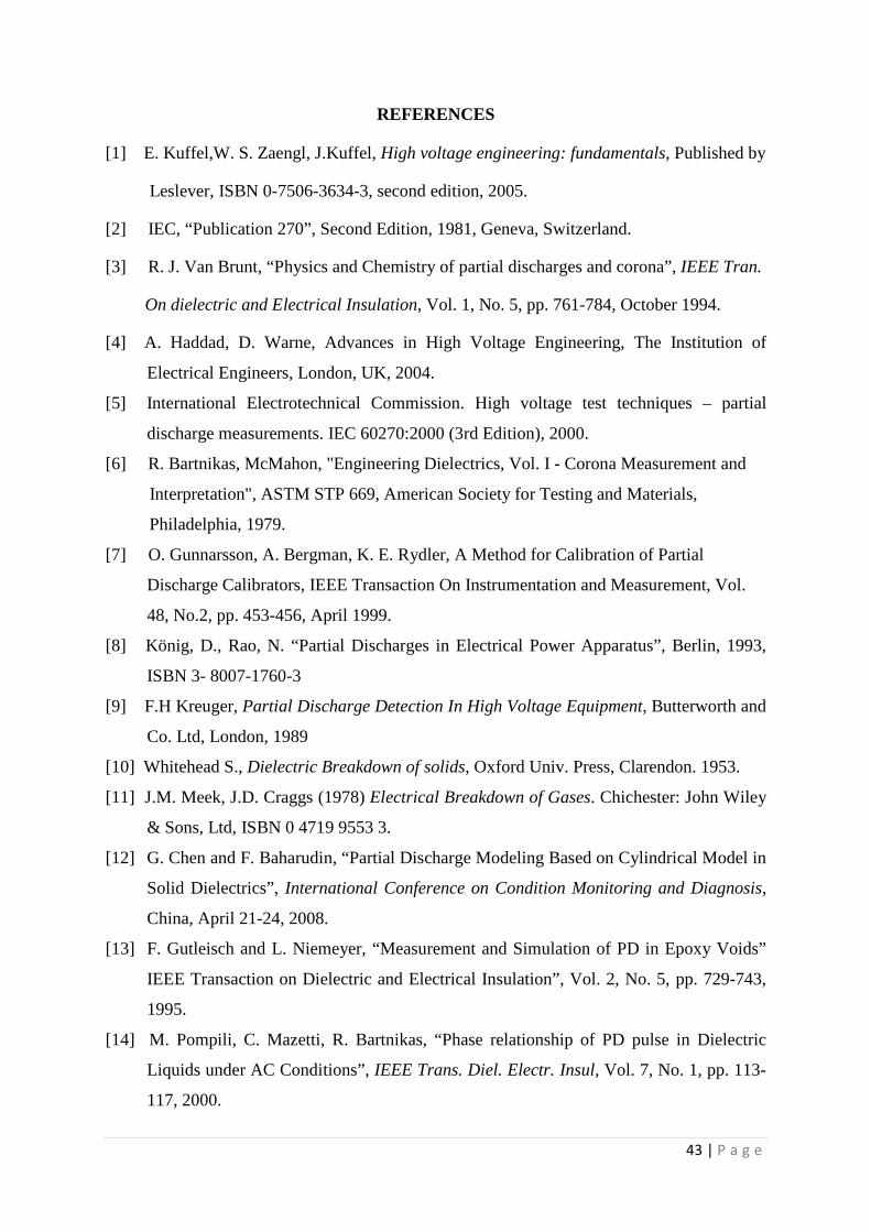
REFERENCES
[1] E. Kuffel,W. S. Zaengl, J.Kuffel, High voltage engineering: fundamentals, Published by
Leslever, ISBN 0-7506-3634-3, second edition, 2005.
[2] IEC, “Publication 270”, Second Edition, 1981, Geneva, Switzerland.
[3] R. J. Van Brunt, “Physics and Chemistry of partial discharges and corona”, IEEE Tran.
On dielectric and Electrical Insulation, Vol. 1, No. 5, pp. 761-784, October 1994.
[4] A. Haddad, D. Warne, Advances in High Voltage Engineering, The Institution of
Electrical Engineers, London, UK, 2004.
[5] International Electrotechnical Commission. High voltage test techniques – partial
discharge measurements. IEC 60270:2000 (3rd Edition), 2000.
[6] R. Bartnikas, McMahon, "Engineering Dielectrics, Vol. I - Corona Measurement and
Interpretation", ASTM STP 669, American Society for Testing and Materials,
Philadelphia, 1979.
[7] O. Gunnarsson, A. Bergman, K. E. Rydler, A Method for Calibration of Partial
Discharge Calibrators, IEEE Transaction On Instrumentation and Measurement, Vol.
48, No.2, pp. 453-456, April 1999.
[8] König, D., Rao, N. “Partial Discharges in Electrical Power Apparatus”, Berlin, 1993,
ISBN 3- 8007-1760-3
[9] F.H Kreuger, Partial Discharge Detection In High Voltage Equipment, Butterworth and
Co. Ltd, London, 1989
[10] Whitehead S., Dielectric Breakdown of solids, Oxford Univ. Press, Clarendon. 1953.
[11] J.M. Meek, J.D. Craggs (1978) Electrical Breakdown of Gases. Chichester: John Wiley
& Sons, Ltd, ISBN 0 4719 9553 3.
[12] G. Chen and F. Baharudin, “Partial Discharge Modeling Based on Cylindrical Model in
Solid Dielectrics”, International Conference on Condition Monitoring and Diagnosis,
China, April 21-24, 2008.
[13] F. Gutleisch and L. Niemeyer, “Measurement and Simulation of PD in Epoxy Voids”
IEEE Transaction on Dielectric and Electrical Insulation”, Vol. 2, No. 5, pp. 729-743,
1995.
[14] M. Pompili, C. Mazetti, R. Bartnikas, “Phase relationship of PD pulse in Dielectric
Liquids under AC Conditions”, IEEE Trans. Diel. Electr. Insul, Vol. 7, No. 1, pp. 113-
117, 2000.

44 | P a g e
[15] O. Gunnarsson, “Calibration of PD-calibrators,” SP Rep 1998:01, SP Swedish Nat.
Testing and Res. Inst., Boras, Sweden, 1998.
[16] G. Mole, Basic characteristics of corona detector calibrators, Trans. IEEE, PAS 89
(1970)2, p.198-204.
[17] G. Crotti,, S. D‘Emilio, P. A. Giorgi, O. Sarcco, “System for calibration of partial
discharge calibrators”, 9th ISH, pp 4511-1-3; Graz 1995.
[18] K. Schon and W. Lucas, “Intercomparison of impulse charge measurements,” PTB,
Braunschweig, Germany, 1998.
[19] K. Schon and H.D. Valentini, “Programmable impulse charge generator for calibrating
PD instruments,” Proc. 10th ISH, Montreal, 1997.
[20] R. Gobbo, G. Pesavento, A. Sardi, O. Cherbaucich, G. Rizzi, “Influence quantities in
the calibration of PD calibrators, contribution to the uncertainty estimate”, Proc. 11t,
ISH, London, pp 5.272.p5 – 5.275.p5, 1999.