Embed Size (px)
Citation preview
© Cambridge Silicon Radio 2011
Modeling of High Performance HV MOSFETTransistors in a 40nm Technology Node
Rainer Herberholz, Yoan Dupret, Sunil Chitrashekaraiah, David Riedner, Seán Minehane, David Vigar and Mark Redford CSR, Advanced Process Technology Development (APTD)
Heidrun Alius, Simon Knecht and Thomas GneitingAdMOS GmbH, Advanced Modeling Solutions
MOS-AK Workshop, Paris, 7th April 2011
© Cambridge Silicon Radio 2011
Outline
Motivation
HiSIM HV Extraction Flow
Convergence Issues
Corners and Statistical Model
Model Verification
Conclusion
Page 2
© Cambridge Silicon Radio 2011
Motivation
Page 3
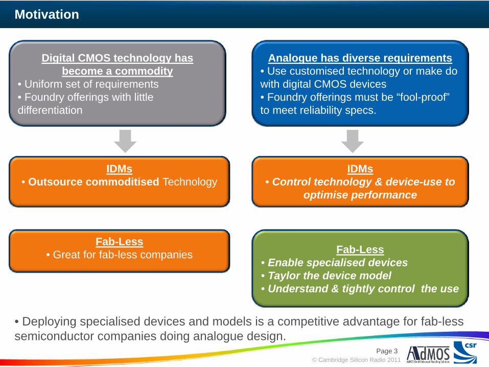
Digital CMOS technology hasbecome a commodity
• Uniform set of requirements• Foundry offerings with little differentiation
Analogue has diverse requirements• Use customised technology or make do with digital CMOS devices• Foundry offerings must be “fool-proof” to meet reliability specs.
IDMs• Outsource commoditised Technology
Fab-Less• Enable specialised devices• Taylor the device model• Understand & tightly control the use
Fab-Less• Great for fab-less companies
IDMs• Control technology & device-use to
optimise performance
• Deploying specialised devices and models is a competitive advantage for fab-less semiconductor companies doing analogue design.

© Cambridge Silicon Radio 2011
CSR HV-MOS in 40nm Low-Power CMOS
Page 4
With no control of the use condition, the foundry HV-MOS must be conservative to pass device qual.
– RDS,ON & capacitances are compromised
CSR has characterised a customised HV-MOS in TSMC 40LP with performance and reliability tailored to the application in
– Power management– RF applications
Standard 52Å gate-oxide & well-Implants, triple well
HiSIM HV was chosen to correctly represent critical DC & AC device properties
Notes:– 40nm CMOS is a x0.9 shrink of 45nm layout dimensions.– Electrical data is relative to shrink dimensions

© Cambridge Silicon Radio 2011
CSR 40nm HV-MOS Device Performance
CSR HV-MOS key device properties:– L=0.297um is default for use at VDD=5V– For shorter L, reliability must be considered for each use case
Page 5
.
P-Well
STI
N-Well
.
N-Well
STI
P-Well
NMOSL=0.225um
NMOS,L=0.297um
PMOS,L=0.225um
PMOS,L=0.297um
BVDS >10V, limited by well-breakdownRDSON @ VG=2.5V(mΩmm2) 23 25 52 59
Ioff (pA/um) 40 <1 4 <1
NMOS
L L
NMOS PMOS
Notes: L is the length of the inversion channel (model-parameter C)
Device Cross-sectionTransit-Frequency

© Cambridge Silicon Radio 2011
Model Parameter Extraction Flow
• Measured data on multiple wafers
• CHALLENGE: Limited amountof data prior tovolume production. Lot-2-lot variation must be estimated initially
• Measured ring oscillator data
• Measureddata from twoprocess lots
DC, CV Timing
MismatchCorner, ProcessVariation
Page 6
© Cambridge Silicon Radio 2011
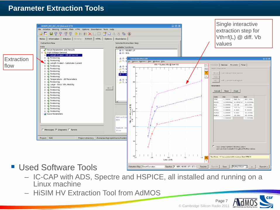
Parameter Extraction Tools
Used Software Tools– IC-CAP with ADS, Spectre and HSPICE, all installed and running on a
Linux machine – HiSIM HV Extraction Tool from AdMOS
Extractionflow
Single interactiveextraction step forVth=f(L) @ diff. Vbvalues
Page 7

© Cambridge Silicon Radio 2011
Typical Parameter Extraction Setup
Model complexity and the overlay of many effects (self heating, quasi saturation, velocity saturation, ..) required the simultaneous adjustment of different device characteristics like id-vg, id-vd, gm, gds, …
Configurableplot area
Optimizer / Tuner for parameteradjustment
Page 8
© Cambridge Silicon Radio 2011
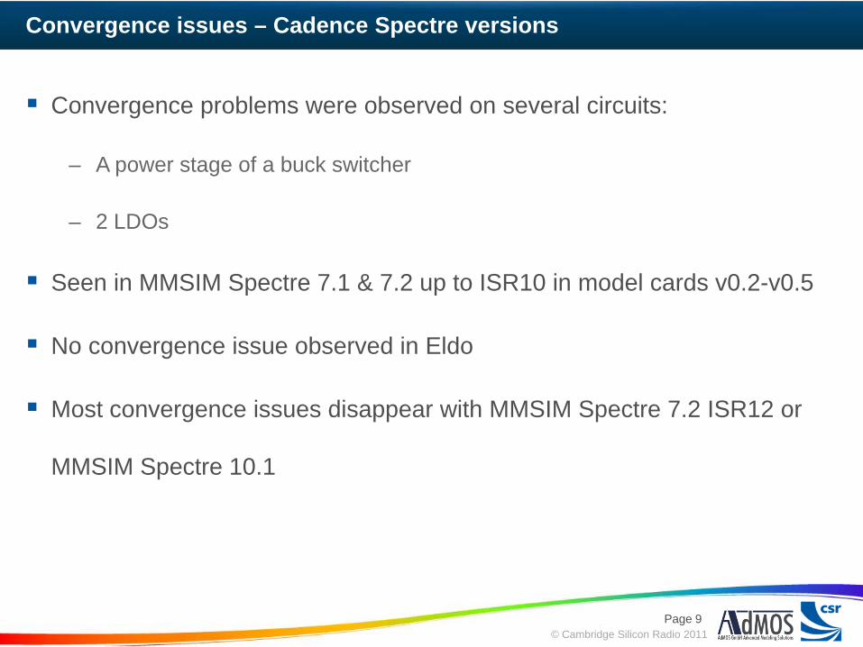
Convergence issues – Cadence Spectre versions
Page 9
Convergence problems were observed on several circuits:
– A power stage of a buck switcher
– 2 LDOs
Seen in MMSIM Spectre 7.1 & 7.2 up to ISR10 in model cards v0.2-v0.5
No convergence issue observed in Eldo
Most convergence issues disappear with MMSIM Spectre 7.2 ISR12 or
MMSIM Spectre 10.1
© Cambridge Silicon Radio 2011
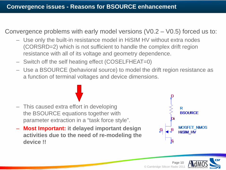
Convergence issues - Reasons for BSOURCE enhancement
Page 10
Convergence problems with early model versions (V0.2 – V0.5) forced us to:– Use only the built-in resistance model in HiSIM HV without extra nodes
(CORSRD=2) which is not sufficient to handle the complex drift region resistance with all of its voltage and geometry dependence.
– Switch off the self heating effect (COSELFHEAT=0)– Use a BSOURCE (behavioral source) to model the drift region resistance as
a function of terminal voltages and device dimensions.
– This caused extra effort in developing the BSOURCE equations together with parameter extraction in a “task force style”.
– Most Important: it delayed important design activities due to the need of re-modeling the device !!
© Cambridge Silicon Radio 2011
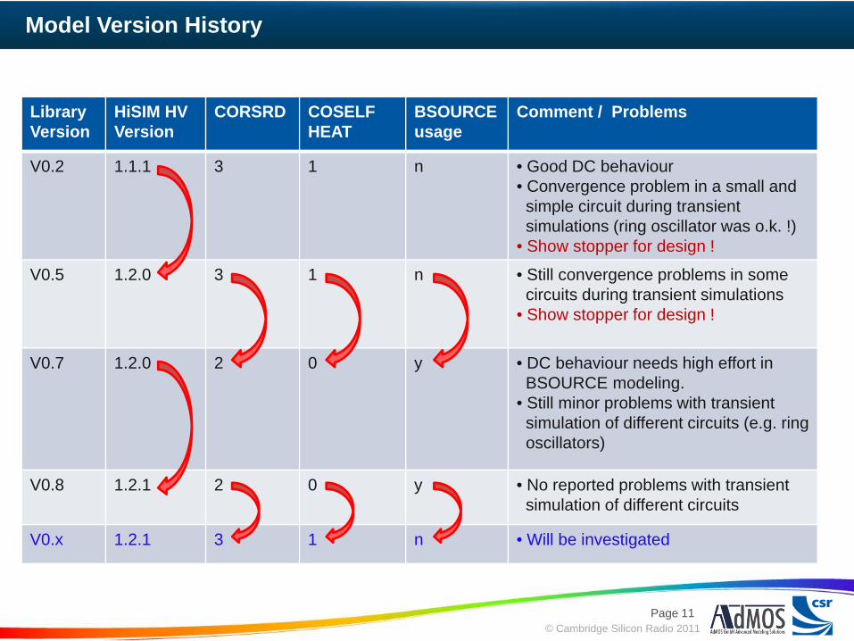
Model Version History
Library Version
HiSIM HV Version
CORSRD COSELFHEAT
BSOURCE usage
Comment / Problems
V0.2 1.1.1 3 1 n • Good DC behaviour• Convergence problem in a small and simple circuit during transient simulations (ring oscillator was o.k. !)
• Show stopper for design !
V0.5 1.2.0 3 1 n • Still convergence problems in some circuits during transient simulations
• Show stopper for design !
V0.7 1.2.0 2 0 y • DC behaviour needs high effort in BSOURCE modeling.
• Still minor problems with transient simulation of different circuits (e.g. ring oscillators)
V0.8 1.2.1 2 0 y • No reported problems with transient simulation of different circuits
V0.x 1.2.1 3 1 n • Will be investigated
Page 11
© Cambridge Silicon Radio 2011
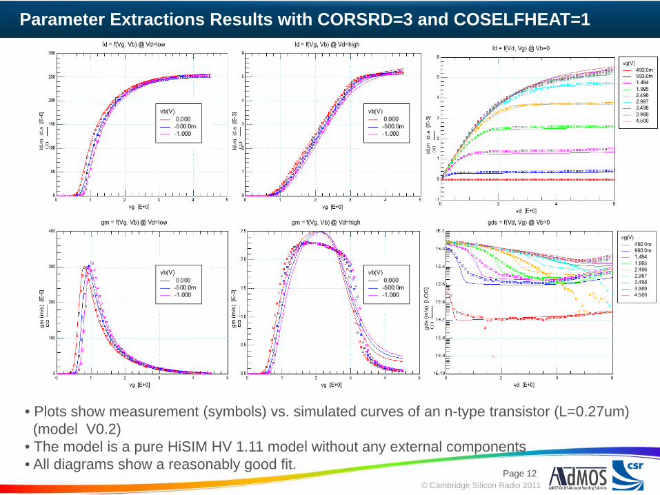
Parameter Extractions Results with CORSRD=3 and COSELFHEAT=1
• Plots show measurement (symbols) vs. simulated curves of an n-type transistor (L=0.27um)(model V0.2)
• The model is a pure HiSIM HV 1.11 model without any external components• All diagrams show a reasonably good fit.
Page 12
© Cambridge Silicon Radio 2011
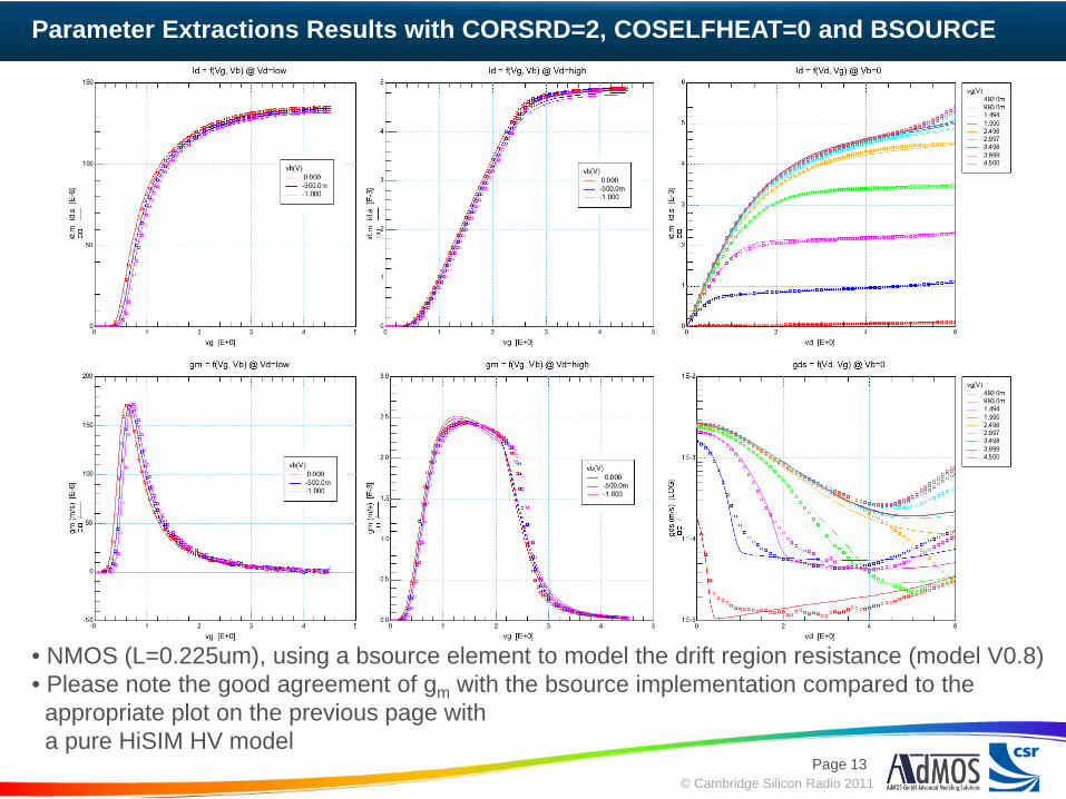
Parameter Extractions Results with CORSRD=2, COSELFHEAT=0 and BSOURCE
• NMOS (L=0.225um), using a bsource element to model the drift region resistance (model V0.8)• Please note the good agreement of gm with the bsource implementation compared to the
appropriate plot on the previous page with a pure HiSIM HV model
Page 13
© Cambridge Silicon Radio 2011
Corner and Process Variations
+3σ: 622mV
SS: 620mVTT: 448mV
-3σ: 275mVFF: 288mV
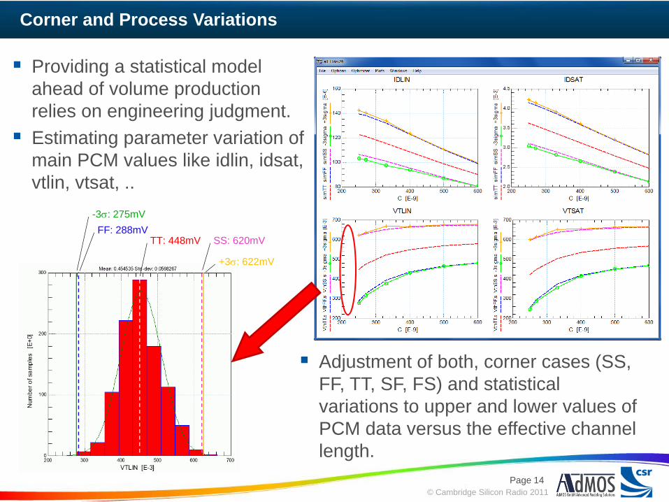
Providing a statistical model ahead of volume production relies on engineering judgment. Estimating parameter variation of main PCM values like idlin, idsat, vtlin, vtsat, ..
Adjustment of both, corner cases (SS, FF, TT, SF, FS) and statisticalvariations to upper and lower values of PCM data versus the effective channel length.
Page 14

© Cambridge Silicon Radio 2011
Parameters for Corner and Process Variation Modeling
Parameter Description Effects / NotesTOX Physical gate oxide thickness
NSUBC Substrate impurityconcentration
Note: VFBC has only limited range (-1.2 .. -0.8) and is not suitable to model variation over a wider range.
SC1 Short channel effect of Vth
MUEPHL Low field mobility Please note: range of MUEPH0is very restricted(0.25<MUEPH0<0.35)
MUEPLP Therefore, MUEPHO is not veryuseful for corner variations.
NINVD Reduced resistance effect forlow Vds
High field mobility
15
( ) ⎟⎟⎠
⎞⎜⎜⎝
⎛
⋅+⋅=
++=
MUEPLPPH
SRPHCB
LMUEPHLMUEPH
6
0
1011
1111
μ
μμμμ
The parameters in the table above have been selected for both, worst case corner modeling as well as for a statistical model which is feasible for Monte Carlo simulations.
Page 15

© Cambridge Silicon Radio 2011
Mismatch Model
Mismatch test structures with diff. L/W have been evaluated on 2 wafers for typical PCM values: vtlin, vtsat, gmmax, idlin, multiple idsat, ...To avoid unrealistic values, outliers had to be removed.Classic mismatch formulacould be applied and resulted in good agreements between measured and simulated values (see vtlin and idsat3 below)
Outliers are not takeninto account
Page 16Note: Idsat3: VG=2.5V, VD=5V

© Cambridge Silicon Radio 2011
Parameters applied for Mismatch Variation Modeling
Parameter Description Effects / NotesNSUBC Substrate impurity
concentrationThreshold voltage
SC1 Short channel effect of Vth
SC2 Short channel effect of Vth athigh drain voltage
MUECB1 Low field mobility
RDEXTVG Parameters of user definedbsource element which
Saturation region
RDEXTVG1 represents the drift regionresistance
17
The parameters in the table above have been selected for the modeling of the mismatch behaviour.
Page 17

© Cambridge Silicon Radio 2011
Timing Verification using Ring Oscillator Measurements
The timing behaviour of the models is evaluated by the simulation of ring oscillator circuits.Details:
– 199 Stages– Enable/Disable Feature– Output buffer and divider
Measurements are done at:– Temperatures between -40°C and
125°C– Supply voltages VDD between
1.5V and 4.0VThe models fit well without changes inside the given tolerance
Page 18
© Cambridge Silicon Radio 2011
Summary/Conclusion
Fab-less companies need control over special devices to
compete with IDMs in the analogue space
The presentation describes a complete modeling flow used by a
fab-less company
Limited access to statistical data prior to volume production
requires careful estimation of production variation
Critical convergence problems occurred with HiSIM HV (different
model versions) in Spectre (different versions). This caused a
delay in very important design activities.
Workaround: Apply old style solution to model drift region using a
resistor.
Page 19

© Cambridge Silicon Radio 2011
Thank you