Embed Size (px)
Citation preview

9000 Virginia Manor Rd Ste 290, Beltsville MD 20705 | 301-474-0607 | www.dfrsolutions.com
Modeling Printed Circuit Boards
with Sherlock 3.2
DfR Solutions – September 23, 2014
Presented by:
Dr. Nathan Blattau – Senior Vice President

Who is DfR Solutions?
The Industry Leader in
Quality-Reliability-Durability
of Electronics 50 Fastest Growing Companies in the Electronics Industry - Inc Magazine
2012 Global Technology Award Winner
Best Design Verification Tool - Printed Circuit Design

• Printed Circuit Boards (PCB), also known as
– Printed Wiring Boards (PWB)
– Circuit Cards, etc..
• Provides mechanical support and electrical interconnects to the electronic components
• Basic Materials
– Conductors
– Dielectric or insulator
– Structural reinforcement
• Woven glass cloth
• Fibers
• Must be able to provide the necessary:
– Electrical performance
– Structural performance
– Survive manufacturing
• IPC-4101 - Specification for Base Materials for Rigid and Multilayer Printed Boards
– Covers the requirements for base materials that are referred to as laminate or prepreg. These are to be used primarily for rigid and multilayer printed boards for electrical and electronic circuits.

• Composite material
– Reinforcement (glass cloth)
– Polymer (resin)
– Copper
Printed Circuit Board
copper
Glass fibers
polymer

• PCB laminates (and prepregs) are fabricated with a variety of glass styles
• Problem: All datasheet properties are for laminate with 7628 glass style
– Most laminate (and prepreg) in complex PCBs have a low volume fraction of glass (i.e., 1080 or 106)
Glass Style Glass Style
Resin Volume Content
Fiber Volume Content
1027 0.86 0.14
1037 0.86 0.14
106 0.84 0.16
1067 0.84 0.16
1035 0.83 0.17
1078 0.82 0.18
1080 0.79 0.21
2313 0.74 0.26
2116 0.71 0.29
3313 0.71 0.29
3070 0.68 0.32
1647 0.66 0.34
1651 0.66 0.34
2165 0.66 0.34
2157 0.66 0.34
7628 0.64 0.36
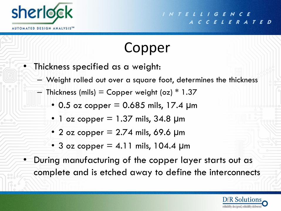
• Thickness specified as a weight:
– Weight rolled out over a square foot, determines the thickness
– Thickness (mils) = Copper weight (oz) * 1.37
• 0.5 oz copper = 0.685 mils, 17.4 µm
• 1 oz copper = 1.37 mils, 34.8 µm
• 2 oz copper = 2.74 mils, 69.6 µm
• 3 oz copper = 4.11 mils, 104.4 µm
• During manufacturing of the copper layer starts out as
complete and is etched away to define the interconnects
Copper

• Two types of resins (not including composition) are
used:
– Pre-preg – partially cured resin that flows and fills in all the
etched away copper features, cures during the pressing
process, does not have copper on it
– Laminate – fully cured resin that typically has copper foil
already attached to it
• There are many different types of resin systems
– Dicy
– Phenolic, etc..
Resin

• PCB materials are frequently under specified! Some
common issues:
– PCB supplier frequently allowed to select laminate material
– No restrictions on laminate changes
– Generic IPC slash sheet requirements used
– Laminates called out by Tg only and with no measurement method
specified
– No cleanliness requirements specified
– Failure to specify stackup
• Not all laminates are created equal
– Failure to put some controls in places opens the door to failure
PCB Materials / Laminate Selection

• Historically, two material properties of concern – Out-of-plane coefficient of thermal expansion (CTEz)
– Out-of-plane elastic modulus (‘stiffness’)(Ez)
– These drive fatigue of the plated through holes
• Key Assumption: No exposure to temperatures above the glass transition temperature (Tg) (field environment)
• The two material properties (CTE and E) are driven by choices in resin, glass style, and filler
• Additional concern is in-plane properties (solder joint fatigue)
PCB Materials and Reliability

• Is the amount a material expands when exposed to a change in temperature
• It is unlikely that the designer or end user will be able to influence the component properties – Component packaging is typically driven by the die and assembly
– Passing of JEDEC level package tests
– May be able to pick parts with different lead frame materials
• Printed wiring board properties – Designer can influence printed wiring board properties
• Glass style
• Laminate type
• Copper
• Thickness
• This is one of the main factors that drive solder joint fatigue
Coefficient of Thermal Expansion

• In the past most electronic packages had CTE values closer to that of copper, 17.6 ppm/°C
• Larger die and smaller packages have driven a reduction in the component CTE, examples: – Leadless ceramic chip resistors – 5.6 ppm/°C
– QFN (quad flat no-leads) – 8 to 12 ppm/°C
• The CTE of the laminates has decreased over the years – The PCB laminate manufactures do not make it easy to determine
the CTE of their laminate
Influence of Board Properties

• Elimination of leaded devices
– Provides lower RC and higher package densities
– Reduces compliance
Solder Joint Fatigue
Cycles to failure
-40 to 125C QFP: >10,000
BGA: 3,000 to 8,000
QFN: 1,000 to 3,000 CSP / Flip Chip: <1,000

• Realistic target for board CTE is between 15 and 17 ppm/°C
• Most laminate suppliers provide CTExy values
• Key concern, these values are typically for a low resin content laminate (46%-50% resin content by weight, 7628 glass style)
• However the most popular laminates have much higher resin contents – Higher resin content = higher CTE
– Lower modulus
Effect of Glass Style
x
y
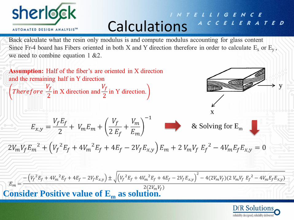
& Solving for Em
Consider Positive value of Em as solution.
Calculations

• Modulus decreases as resin content increases
• CTE increases as resin content increases
• Copper content plays a significant role
• These values can be now used to predict solder joint fatigue
Effect of Glass Style, Exy and CTExy

Glass Style Modulus of Elasticity Ez (MPa) CTEz (ppm)
1027 4380.4 73.9
1037 4380.4 73.9
106 4478.2 72.3
1067 4478.2 72.3
1035 4528.7 71.5
1078 4580.3 70.7
1080 4742.7 68.4
1086 4799.3 67.6
2313 5040.4 64.4
2116 5237.6 62.0
3313 5237.6 62.0
3070 5450.9 59.7
1647 5603.1 58.1
1651 5603.1 58.1
2165 5603.1 58.1
2157 5603.1 58.1
7628 5764.0 56.5
Examples - Glass Style, Modulus Ez and CTEz

• Another key factor is copper thickness
• CTE of copper is about 17 ppm/°C
• One would expect that as the copper thickness increases the CTE of the board would approach this – This is rarely the case
– Thicker copper means larger gaps when the copper is removed, more resin is required to fill those gaps
• When faced with thick copper layers board shops will dramatically increase the prepreg resin content to make manufacturing easier
• This dramatically increases the CTE of the Board
Additional Factors to CTE

Examples
• Boards with thick copper have a lot of resin (higher CTE)
CTE ≈ 15 ppm/C
CTE ≈ 21 ppm/C

9000 Virginia Manor Rd Ste 290, Beltsville MD 20705 | 301-474-0607 | www.dfrsolutions.com
™
3.2

• Adds additional tools for more detailed modeling of the printed circuit board – Stackup tool now allows for the selection of
• Glass Style
• Fiber Material
– The material selected determine the overall material properties used during FEA analysis for the selected laminate
– Laminate manager tool
– Detailed FEA modeling options for PCBs
• New 3D part viewer
• Lead modeling
• Improved ODB++ parsing
Sherlock 3.2

Improved Stackup Tool • When specifying glass style
Sherlock back calculates the properties of the resin based upon the entered datasheet values (7628 glass style)
• The effect of different glass styles can then be calculated
• The properties of the fibers can also be changed
• Sherlock assumes resin in the copper layer gaps

• Sherlock now allows one to add through hole leads to select components
• As expected adding features greatly increases the FEA model complexity
• 3D part viewer shows the part
Lead Modeling

9000 Virginia Manor Rd Ste 290, Beltsville MD 20705 | 301-474-0607 | www.dfrsolutions.com 23
• High Fidelity PCB – Newest Feature
• Sherlock can identify and mesh copper feature within a PCB or substrate
• Provides unrivaled insight into risks due to warpage, thermal issues, mechanical loads, etc.

Detailed FEA PCB Modeling
Mosaic technique, material properties are averaged over the individual elements
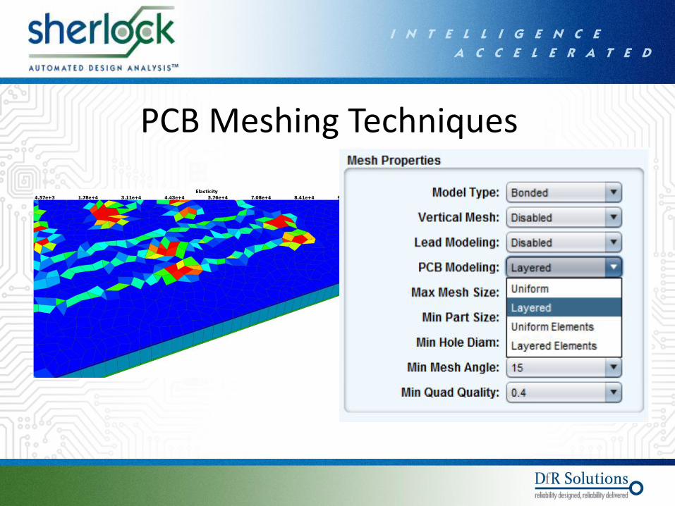
PCB Meshing Techniques

• Uniform model, homogeneous properties for the whole board
• Layered model, homogenous properties per layer (layers have different mechanical properties)
Meshing Techniques

• Uniform elements model, mechanical properties vary only in-plane
• Layered elements model, each element has properties computed based on location and layer
Meshing Techniques, cont

Lead Modeling

Lead Modeling (cont.)
Bonded model with leads on all through
hole components

Sherlock automatically post-processes the FEA results to make predictions for lead vibration fatigue
Lead Modeling (cont.)

• Sherlock 3.2
• More accurate modeling of printed
circuit boards
• The ability to conduct more complex
simulations

32
Thank you!
Nathan Blattau
1-301-640-5821
Tom O’Connor
301-640-5812
Questions??