Embed Size (px)
Citation preview

MODELLING AND PERFORMANCE EVALUATION OF
COUPLED MICRO RESONATOR ARRAY FOR
ARTIFICIAL NOSE
By
Nor Hayati Saad
A thesis submitted to
The University of Birmingham
for the degree of
DOCTOR OF PHILOSOPHY
School of Mechanical Engineering
The University of Birmingham
August 2010

University of Birmingham Research Archive
e-theses repository This unpublished thesis/dissertation is copyright of the author and/or third parties. The intellectual property rights of the author or third parties in respect of this work are as defined by The Copyright Designs and Patents Act 1988 or as modified by any successor legislation. Any use made of information contained in this thesis/dissertation must be in accordance with that legislation and must be properly acknowledged. Further distribution or reproduction in any format is prohibited without the permission of the copyright holder.

ABSTRACT
This research presents a new sensor structure, the coupled micro resonator array (CMRA) as
an approach to reduce the complexity of large artificial nose sensing system. The aim is to
exploit multiple resonant sensors with a simplified readout. The CMRA working principle is
based on mass loading frequency response effect; the frequency response of the coupled
resonators is a signature for the multiple sensors.
The key research outputs are balanced effective mass of the coupled resonators for
measurable response and broke the structure symmetry for unique frequency response pattern
and stable structure eigenvectors to enhance the system odour discrimination.
To develop the CMRA, the structure is modelled and analysed using finite element and
lumped mass analysis. Using silicon-on-insulator material, the CMRA is fabricated in order to
evaluate the performance. The effect of mass loading is tested by platinum mass deposition
using focused ion beam technology (FIB). The inverse eigenvalue analysis was used to
estimate the mass change pattern of the CMRA structure. The research also investigates
effect of the manufacturing variations on the CMRA structure performance.
With the finger print of the coupled frequency response, the output signal of N multiple
resonant sensors is monitored by a single processor; hence, reducing the complexity of
readout and signal processing system.

To my husband Abdul Rahim To my husband Abdul Rahim To my husband Abdul Rahim To my husband Abdul Rahim andandandand
my daughtermy daughtermy daughtermy daughterssss Nur Aisyah Dami Nur Aisyah Dami Nur Aisyah Dami Nur Aisyah Damia and Nurin Safwania and Nurin Safwania and Nurin Safwania and Nurin Safwani

ACKNOWLEDGEMENTS
It is a great pleasure to acknowledge all assistance and support that I directly or indirectly
receive from individual or group of people throughout the whole of my research time until the
completion of this research study.
This research work would not have been produced without my supervisor Michael CL
Ward. I am very grateful and thankful for his enthusiastic support and guidance, for all
research ideas, and for support in order for me to complete this research thesis. Many thanks
as well to my second supervisor Raya K. Al-Dadah for her moral support when I started my
research and until the research has been completed.
Special thank to Carl J. Anthony for his invaluable ideas, tips and support throughout
my time in the clean room to fabricate the structure. Many thanks to my research colleague
Xueyong Wei for his help in HF released process and platinum mass deposition using focused
ion beam machine (FIB); thank you to David Chenelar for his help in gold metallization;
Simon Pyatt (Physics Department) for structure wire bonding; Mike Lancaster and Donna
Holdom (Electrical Engineering Department) in allowing me to use the wafer dicing saw
machine; Paul Stanley and Morris Theresa (Metallurgy Department), and Hossein Ostadi for
their help in using the scanning electron microscope.
I would like to specially thank Ross Turnbull, research colleague from Oxford
University, who was responsible for the establishment of the electronic testing setup; other
research fellow Bhaskar Choubey, and Steve Collins for their research knowledge and
support. To thank to QinetiQ for the aluminium metallization, the Engineering and Physical
Sciences Research Council (EPSRC) which indirectly or directly finance some of the research
cost.
Thank you as well to other fellow researchers, Mi Yeon Song, Jason Teng, Martin J
Prest and Peng Bao in sharing some research knowledge. Not to forget all research
colleagues in Micro Technology Group, Emma Carter, Sam, Haseena, Ali, and Sahand who
cheered up my time and shared their research ideas.
Thank you so much to all my family members, my husband Abdul Rahim, my mother
Fatimah who supported me throughout my research time.
Finally, I would like to gratefully acknowledge the MARA University of Technology
(UiTM) Shah Alam and the Malaysian Ministry of Higher Education for sponsoring my PhD
study.

LIST OF PUBLICATION
1) Nor Hayati Saad, Michael C L Ward, Raya Al-Dadah, Carl Anthony, Bhaskar Choubey,
and Steve Collins. Performance Analysis of A Coupled Micro Resonator Array Sensor.
Eurosensors XXII, Dresden, Germany, ISBN 978-3-00-025218-1, pp. 60 – 63, 2008.
2) Nor Hayati Saad, Raya K. Al-Dadah, Carl J. Anthony, and Michael C.L. Ward. MEMS
Mechanical Spring in Coupling and Synchronizing Coupled Micro resonator Array
Sensor (Extended Abstract). 34th
International Conference on Micro & Nano
Engineering, Athens, Greece, 2008.
3) Nor Hayati Saad, Raya K. Al-Dadah, Carl J. Anthony, and Michael C.L. Ward.
Analysis of MEMS Mechanical Spring for Coupling Multimodal Micro Resonators
Sensor. Microelectronic Engineering, 86(4-6):1190-1193, 2009.
4) Nor Hayati Saad, Xueyong Wei, Carl Anthony, Hossein Ostadi, Raya Al-Dadah, and
Michael C.L. Ward. Impact of Manufacturing Variation on the performance of
Coupled Micro Resonator Array for Mass Detection Sensor. Eurosensors XXIII,
Switzerland; or Procedia Chemistry, 1(1): 831-834, 2009.
5) Nor Hayati Saad, Carl J. Anthony, Raya Al-Dadah, Michael C.L. Ward. Exploitation of
Multiple Sensor Arrays in Electronic Nose. 2009 IEEE Sensors, pp.1575-1579, 2009.
6) Nor Hayati Saad, Carl J. Anthony, Michael C.L. Ward, Bhaskar Choubey, Ross
Turnbull, and Steve Collins. Manufacturing Variation in MEMS: Fabrication of Micro
Array Resonators. Second STIMESI Workshop on MEMS and Microsystems Research
and Teaching, Berlin-Brandenburg Academy of Sciences and Humanities, Germany,
2008.

TABLE OF CONTENTS
CHAPTER 1 - INTRODUCTION
1.1 Introduction to the Artificial Nose .................................................................................................................................................... 1
1.2 Problem Statement .................................................................................................................................................................................................. 3
1.3 Coupled Micro Resonator Array (CMRA) ............................................................................................................................ 5
1.4 Manufacturing Process Variation versus CMRA Performance ................................................................7
1.5 Objectives ............................................................................................................................................................................................................................ 8
1.6 Scope and Methodology .................................................................................................................................................................................. 8
1.7 Outline of Thesis ........................................................................................................................................................................................................ 9
CHAPTER 2 - LITERATURE REVIEW
2.1 Introduction ................................................................................................................................................................................................................... 11
2.2 Biological Nose versus Artificial Nose .................................................................................................................................. 11
2.2.1 The Importance of the Artificial Nose................................................................................................................. 14
2.3 Sensor Technologies Used in the Artificial Noses ................................................................................................. 15
2.3.1 Sensor Type and Features ..................................................................................................................................................... 15
2.3.2 Performance of Current Sensors and Artificial Noses .................................................................. 18
2.4 Resonant Sensors Performance.......................................................................................................................................................... 20
2.4.1 Quality Factor ........................................................................................................................................................................................ 21
2.4.2 Nonlinear Effect ................................................................................................................................................................................. 23
2.4.3 Resonance Frequency- Temperature Sensitivity................................................................................... 24
2.4.4 Resonator Design and Vibration Mode.............................................................................................................. 25
2.5 Excitation and Detection Methods of Resonant Sensor .................................................................................. 25
2.5.1 Electrostatic Excitation and Capacitive Detection ............................................................................. 26
2.5.2 Dielectric Excitation and Detection ........................................................................................................................ 27
2.5.3 Piezoelectric Excitation and Detection ............................................................................................................... 27
2.5.4 Resistive Heating Excitation and Piezoresistive Detection ................................................... 27
2.5.5 Optical Heating and Detection ....................................................................................................................................... 27
2.5.6 Magnetic Excitation and Detection ......................................................................................................................... 28
2.6 Coupled Resonators ........................................................................................................................................................................................... 29
2.7 Comb-Drive .................................................................................................................................................................................................................. 31

2.7.1 Important Design Criteria of Comb-Drive .................................................................................................... 31
2.7.2 Comb Drive Design for Large and Stable Displacement .......................................................... 33
2.8 Manufacturing Variation in MEMS ............................................................................................................................................ 35
2.8.1 Reducing the Performance Variability of MEMS at the Design Stage ................. 36
2.8.2 Performance Variation Estimation and Process Variation Quantification........ 36
2.9 Summary and Focus of Thesis.......................................................................................................................................................... 38
CHAPTER 3 - DESIGN, MODELLING AND FINITE ELEMENT ANALYSIS OF
CMRA-V1
3.1 Introduction ................................................................................................................................................................................................................... 40
3.2 Constraints and Design Considerations ................................................................................................................................. 40
3.2.1 Drive-Readout System Constraint............................................................................................................................. 41
3.2.2 Expected CMRA Output Signal ................................................................................................................................... 43
3.2.2.1 Distinctive (Unique) Response Pattern..................................................................................... 43
3.2.2.2 Coupling Modes........................................................................................................................................................ 44
3.2.2.3 Measurable (Readable) Signal .............................................................................................................. 44
3.2.3 Fabrication Constraints ............................................................................................................................................................. 44
3.3 Design and Finite Element Analysis of the Fixed-Fixed Beam Resonator .......................... 45
3.3.1 Design Considerations ............................................................................................................................................................... 45
3.3.2 Fixed-Fixed Beam Resonator Design................................................................................................................... 45
3.3.3 Modelling and Finite Element Analysis .......................................................................................................... 47
3.3.3.1 Eigenfrequency of Single Resonator ........................................................................................... 47
3.3.3.2 Effective Mass and Stiffness of Single Resonator .................................................... 48
3.3.3.3 Frequency Response of the Fixed-Fixed Beam Resonator ........................... 49
3.3.4 Performance of the Fixed-Fixed Beam Resonator.............................................................................. 50
3.4 Mechanical Spring Coupling ................................................................................................................................................................ 51
3.4.1 Design Considerations ............................................................................................................................................................... 51
3.4.2 Closed Loop Butterfly Shape Spring Design ............................................................................................. 52
3.4.3 Performance of Butterfly Spring using FEA .............................................................................................. 53
3.4.4 Effect of Coupling Constant .............................................................................................................................................. 55
3.4.5 Uniqueness of CMRA Frequency Response Pattern Analysis using FEA....... 58
3.5 Comb Actuator.......................................................................................................................................................................................................... 61
3.5.1 Design Considerations ............................................................................................................................................................... 61
3.5.2 Comb Actuator Design.............................................................................................................................................................. 61

3.5.3 Finite Element Analysis of Comb Actuator ................................................................................................. 64
3.5.3.1 Effective Mass, Stiffness, and Eigenfrequency ............................................................ 64
3.5.3.2 Generated Capacitance .................................................................................................................................. 65
3.5.4 Performance of Comb Actuator.................................................................................................................................... 67
3.5.5 Driving the CMRA-v1 using the Designed Actuator ..................................................................... 68
3.6 Single Fixed-Fixed Beam Resonator for Frequency Response Measurement................. 69
3.6.1 Finite Element Analysis of the singleR-v1 ................................................................................................... 70
3.6.2 Performance of the SingleR-v1 Structure ....................................................................................................... 71
3.7 Summary and Conclusion ......................................................................................................................................................................... 73
CHAPTER 4 IMPROVEMENT OF CMRA USING LUMPED MASS MODEL
ANALYSIS
4.1 Introduction ................................................................................................................................................................................................................... 75
4.2 Lumped Mass Model of CMRA ...................................................................................................................................................... 75
4.3 Re-evaluation of the CMRA-v1........................................................................................................................................................ 80
4.4 Analysis of Improved Design .............................................................................................................................................................. 81
4.5 Key Structure Improvement of the CMRA-v2 .......................................................................................................... 85
4.5.1 Measurability of Output Signal ..................................................................................................................................... 85
4.5.2 Unique Frequency Response Pattern ..................................................................................................................... 85
4.5.3 Stability of Eigenvectors ........................................................................................................................................................ 86
4.6 Lumped Mass Model of the CMRA-v2 and Structural Analysis ....................................................... 86
4.6.1 CMRA-v2 for Measurability of Output Signal ....................................................................................... 86
4.6.2 Breaking Structure Symmetry for Performance Improvement of CMRA ...... 87
4.6.3 Result and Discussion................................................................................................................................................................. 90
4.7 Summary and Conclusion ......................................................................................................................................................................... 95
CHAPTER 5 - MODELLING, FINITE ELEMENT ANALYSIS AND PERFORMANCE
EVALUATION OF CMRA-V2
5.1 Introduction ................................................................................................................................................................................................................... 98
5.2 Improved Design of CMRA................................................................................................................................................................... 98
5.2.1 Five Constant Mass CMRA ............................................................................................................................................... 99
5.2.2 Five Staggered CMRA .......................................................................................................................................................... 101
5.3 Modelling and Finite Element Analysis of CMRA ........................................................................................... 103
5.3.1 Eigenfrequency and Eigenmode .............................................................................................................................. 104

5.3.2 Frequency Response Pattern of the Unperturbed CMRA .................................................... 107
5.3.3 Effective Mass and Effective Stiffness........................................................................................................... 110
5.3.4 Change in Comb-Drive Capacitance ................................................................................................................. 111
5.4 Performance Evaluation of the CMRA-v2: Lumped Mass Analysis........................................ 113
5.4.1 Analysis Overview ...................................................................................................................................................................... 113
5.4.2 Result and Discussion: Frequency Response Pattern of CMRA ................................ 115
5.4.3 Result and Discussion: Stability of System Eigenvectors of CMRA................... 120
5.5 Estimation of Mass Change Patterns of the CMRA Using Inverse Eigenvalue
Analysis ......................................................................................................................................................................................................................... 123
5.5.1 Overview and Analysis ......................................................................................................................................................... 123
5.5.2 Result and Discussion............................................................................................................................................................. 125
5.6 Impact of Manufacturing Variation on the CMRA performance ................................................... 126
5.6.1 Manufacturing Variation Quantification ...................................................................................................... 126
5.6.1.1 Overview ......................................................................................................................................................................... 126
5.6.1.2 The Variation Quantification and Statistical Data Analysis ................... 128
5.6.1.3 Result and Discussion................................................................................................................................... 129
5.6.2 Impact of Manufacturing Variation Analysis ........................................................................................ 131
5.6.2.1 Result and Discussion................................................................................................................................... 133
5.7 Summary and Conclusion ..................................................................................................................................................................... 135
CHAPTER 6 - FABRICATION AND PACKAGING
6.1 Introduction ............................................................................................................................................................................................................... 139
6.2 Single-Crystal Silicon and Silicon-on-Insulator Materials ................................................................... 139
6.3 Overview of the Fabrication Process Flow and Structure Packaging ...................................... 141
6.4 Mask Design ............................................................................................................................................................................................................ 143
6.4.1 Type of mask....................................................................................................................................................................................... 144
6.4.2 Etching Channel Aspect Ratio.................................................................................................................................... 144
6.4.3 Size of the Suspended and Anchored Structure ................................................................................. 145
6.4.4 Size of Wire Bonded Pad................................................................................................................................................... 146
6.4.5 Gap and Alignment for Chip Dicing Requirement ........................................................................ 146
6.5 Detail Fabrication Processes.............................................................................................................................................................. 147
6.5.1 Soft Wafer Cleaning ................................................................................................................................................................. 147
6.5.2 Primer and Resist Coating ................................................................................................................................................ 147
6.5.3 Pattern Transfer Using Lithography and Development Process ................................. 148

6.5.4 Reactive Ion Etching Process..................................................................................................................................... 150
6.5.5 Wafer Cutting Process ........................................................................................................................................................... 151
6.5.6 Chip Cleaning and Stripping off Resist ......................................................................................................... 152
6.5.7 HF Release Process .................................................................................................................................................................... 152
6.5.8 Structure Movement Observation .......................................................................................................................... 154
6.6 Structure Observations............................................................................................................................................................................... 154
6.6.1 Observation 1: Photolithography and Development Process .......................................... 155
6.6.2 Observation 2: Reactive Ion Etching ............................................................................................................... 158
6.6.3 Observation 3: Before HF Release Process.............................................................................................. 158
6.6.4 Observation 4: HF Release Process .................................................................................................................... 160
6.6.5 Fabrication Constraints and Discussion ........................................................................................................ 161
6.7 Preparation for Electronic Testing ............................................................................................................................................ 162
6.7.1 Gold Metallisation ....................................................................................................................................................................... 162
6.7.2 Aluminium Metallisation ................................................................................................................................................... 164
6.7.3 Wire Bonding and Structure Packaging for Electronic Testing................................... 165
6.8 Material Deposition Using FIB ..................................................................................................................................................... 168
6.9 Summary and Conclusion ..................................................................................................................................................................... 169
CHAPTER 7 - FREQUENCY RESPONSE MEASUREMENT, RESULT AND
DISCUSSION
7.1 Introduction ............................................................................................................................................................................................................... 171
7.2 Aim of Electronic Testing..................................................................................................................................................................... 171
7.3 Electronic Testing Setup and Measurement Scheme ...................................................................................... 172
7.3.1 Overview of the Electronic Testing Setup ................................................................................................. 172
7.3.2 Measurement Scheme............................................................................................................................................................. 175
7.4 Frequency Response Measurement.......................................................................................................................................... 179
7.4.1 Testing Procedures ...................................................................................................................................................................... 179
7.4.2 Overview of Testing Samples and Testing Conditions............................................................ 181
7.5 Result and Discussion 1: Performance of a Single Resonator ........................................................... 183
7.5.1 Effect of Vacuum Pressure Level .......................................................................................................................... 183
7.5.2 Effect of Vpp Driving Voltage................................................................................................................................... 185
7.5.3 Effect of Manufacturing Process Variation on a Single Resonator ........................ 186
7.5.4 Mass Loading Frequency Response Effect of a Single Resonator .......................... 189
7.6 Result and Discussion 2: Performance of CMRA ............................................................................................... 191
7.6.1 Constant Mass CMRA ........................................................................................................................................................... 191

7.6.1.1 Frequency Response of the Unperturbed Structure and
the Effect of Process Variation ...................................................................................................... 191
7.6.1.2 Uniqueness of the Frequency Response- Constant Mass CMRA ... 195
7.6.1.3 Stability of the Structure Eigenvectors ................................................................................. 198
7.6.2 Staggered Mass CMRA ....................................................................................................................................................... 199
7.6.2.1 Frequency Response of the Unperturbed Structure and
the Effect of Process Variation ..................................................................................................... 199
7.6.2.2 Uniqueness of the Frequency Response- Staggered Mass CMRA 202
7.6.2.3 Stability of the Structure Eigenvectors ................................................................................. 205
7.6.3 Staggered Stiffness CMRA............................................................................................................................................. 205
7.6.3.1 Frequency Response of the Unperturbed Structure and
the Effect of Process Variation ..................................................................................................... 205
7.6.3.2 Uniqueness of the Frequency Response
- Staggered Stiffness CMRA ............................................................................................................... 209
7.6.3.3 Stability of the Structure Eigenvectors ................................................................................. 211
7.7 Stability of the Measured Response ...................................................................................................................................... 212
7.8 Summary and Conclusion ..................................................................................................................................................................... 216
CHAPTER 8 - CONCLUSION AND FUTURE RECOMMENDATIONS
8.1 Conclusion .................................................................................................................................................................................................................. 220
8.2 Future Recommendations ...................................................................................................................................................................... 225
APPENDICES
APPENDIX A: Consideration- Finite Element Analysis (COMSOL Multiphysics) ........A-1
APPENDIX B: MATLAB Codes – Eigenvalue and Eigenvectors Analysis .................................B-1
APPENDIX C: Eigenvectors Stability (Alternative 1 – Alternative 6) ................................................ C-1
APPENDIX D: Eigenvectors of 5 Staggered Mass CMRA ................................................................................. .D-1
APPENDIX E: Eigenvectors of 5 Staggered Stiffness CMRA .........................................................................E-1
APPENDIX F: Effective Mass and Stiffness of Comb-Drive Resonator ........................................... F-1
APPENDIX G: Manufacturing Variation Impact on a Single Comb-Drive Resonator G-1
APPENDIX H: Sample of Geometrical Measurements and Manufacturing
Data Analysis: Measured on a Single In-house Chips ..................................................H-1
LIST OF REFERENCES ............................................................................................................................................................................................. R-1

LIST OF FIGURES
1.1 (a) Electronic Nose Prometheus (Alpha MOS, France);
(b) Second generation of electronic nose (NASA) ..................................................................................................................1
1.2 Architecture of artificial nose system .......................................................................................................................................................2
1.3 Schematic diagram of design concept of coupled resonator array sensor structure ..................6
2.1 (a) A simplified architecture of the conventional artificial nose system;
(b) Human olfactory system ................................................................................................................................................................................11
2.2 Odorant receptors and the organization of the human olfactory system .............................................12
2.3 (a) QCM sensor; (b) an individual packaged of the SnO2 sensor; (c) the array of
SnO2 sensor ; (d) Conducting Polymer sensor; (e) MOSFET sensor .......................................................17
2.4 (a) Viscously damped system with harmonic excitation; (b) Sharpness of resonance ....21
2.5 (a) Nonlinear - mechanical stiffening; (b) Nonlinear - electrical softening ......................................24
2.6 Excitation and detection technique of resonant sensor ..................................................................................................26
2.7 Photograph of the array of fifteen coupled cantilevers ................................................................................................30
2.8 Important design geometry of comb drive ......................................................................................................................................31
2.9 Suspensions and comb finger designs ................................................................................................................................................34
3.1 (a) A simplified schematic of sensing and processing system of an artificial nose
Using CMRA sensor structure; (b) Schematic of CMRA-v1 with 2 ports (I/O). ......................41
3.2 Schematic of a fixed-fixed beam resonator (top view) ..................................................................................................46
3.3 Eigenfrequency analysis result of fixed-fixed beam resonator ...........................................................................47
3.4 Static analysis result of the fixed-fixed beam resonator...............................................................................................48
3.5 Frequency response analysis of fixed-fixed beam resonator .................................................................................50
3.6 Scanning Electron Microscope (SEM) image of zigzag coupling spring ............................................52
3.7 Schematic of a closed loop butterfly coupling spring design................................................................................52
3.8 Static analysis result of butterfly coupling spring .................................................................................................................54
3.9 Eigenfrequency analysis result of the first 6 eigenmodes of butterfly spring ................................55
3.10 Schematic of 5 fixed-fixed beam resonators coupled with butterfly coupling spring ........56
3.11 The effect of coupling constant on the response amplitude of the coupled resonators .....58
3.12 Frequency response analysis result of constant mass CMRA ..............................................................................60
3.13 (a) Driven comb actuator; (b) readout comb actuator;
(c) Geometrical design parameter of the comb fingers..................................................................................................62
3.14 Static analysis result of the driven comb actuator.................................................................................................................65
3.15 Eigenfrequency analysis result of comb actuator ..................................................................................................................65
3.16 Capacitance analysis in electrostatic module ..............................................................................................................................66

3.17 Static capacitance and dc/dy of driven comb analysed using FEA...............................................................67
3.18 Eigenfrequency analysis result of CMRA-v1 (mode 1) ...............................................................................................68
3.19 Schematic of fixed-fixed beam resonator
(rigidly coupled to a simple drive and readout comb actuator) ..........................................................................69
3.20 Fundamental eigenfrequency of the fixed-fixed beam resonator ....................................................................71
3.21 Static capacitance and change of capacitance (dc/dy) of the SingleR-v1 structure ...............72
3.22 (a) Generated electrostatic force [N] at different voltage potential [v];
(b) Static displacement due to the generated electrostatic force .......................................................................72
4.1 Schematic of the 5 CMRA-v1 sensor structures .....................................................................................................................75
4.2 Free body diagram of the five CMRA structure......................................................................................................................76
4.3 Free body diagram of undamped CMRA structure .............................................................................................................78
4.4 Eigenmode analysis result of CMRA-v1 ...........................................................................................................................................81
4.5 Eigenmode analysis result of 2 alternatives structure improvement of CMRA-v1................83
4.6 The schematic of the improved version of CMRA-v2 structure.......................................................................87
4.7 Eigenmode analysis result of 6 alternatives of Staggered CMRA .................................................................90
4.8 Stability of eigenvectors analysis result ..............................................................................................................................................93
5.1 Schematic of 5 Constant Mass CMRA.............................................................................................................................................100
5.2 Schematic of 5 Staggered Mass CMRA .........................................................................................................................................102
5.3 Eigenmodes analyses of 5 Constant Mass CMRA .........................................................................................................105
5.4 Eigenmodes analysis result of 5 Staggered Mass CMRA .....................................................................................105
5.5 Eigenmodes analysis result of 5 Staggered Stiffness CMRA ...........................................................................106
5.6 Schematic of 5 Constant Mass CMRA ; an example of drive point
at R1 and readout point at R5 for frequency response analysis .....................................................................107
5.7 Frequency response analysis result of the CMRA ..........................................................................................................108
5.8 Frequency response analysis result of 5 Constant CMRA (FEA) ..............................................................109
5.9 (a) Eigenfrequency of a single comb-drive resonator;
(b), (c) Static displacement analysis result of comb-drive resonator....................................................110
5.10 Capacitance analysis result of single comb-drive resonator using (FEA) and static
displacement result of the resonator .....................................................................................................................................................112
5.11 Frequency response analysis result of 5 Constant CMRA....................................................................................115
5.12 Frequency Response Result of 5 Staggered Mass CMRA ....................................................................................117
5.13 Frequency Response Result of 5 Staggered Stiffness CMRA .........................................................................119
5.14 Stability of eigenvectors analysis result (Constant Mass CMRA).............................................................121
5.15 Stability of eigenvectors analysis result (Staggered Mass CMRA) .........................................................121
5.16 Stability of eigenvectors analysis result (Staggered Stiffness CMRA)...............................................123

5.17 Eigenvectors stability analysis .....................................................................................................................................................................125
5.18 Impact of manufacturing variation analysis on the CMRA performance ........................................127
5.19 (a) Scanning electron microscope (SEM) images of constant coupled resonators;
(b) Anchor spring; (c) Coupling spring; (d) comb fingers; (e) Linked mass...........................128
5.20 Example of comb finger length measured data distribution. ..............................................................................130
5.21 The effect of manufacturing variation on the Constant Mass CMRA ................................................133
6.1 Process Flow of CMRA Fabrication....................................................................................................................................................141
6.2 Schematic diagram of structure device layers at each of process step .................................................142
6.3 (a) SEM image of comb finger, fabricated using polyester film mask;
(b) A photo of the chrome glass mask for the CMRA-v2 structure fabrication ......................144
6.4 Top view of the resonator design with a minimum channel width of 3µm ...................................144
6.5 Schematic of wire bonded pads of the comb drive resonator ...........................................................................146
6.6 A portion of schematic of mask design with cutting mark and cutting width ...........................147
6.7 (a) PVDF filter media used to filter the resist; (b) The filter fixed to the syringe tip .....148
6.8 Mask aligner machine (PLA-501 FN) for photolithography process ....................................................149
6.9 Surface Technology System (STS machine) ............................................................................................................................150
6.10 (a) DAD 320 (wafer dicing saw machine); (b) Diamond blade;
(c) Wafer stuck on the tape holder and clamped on the vacuum chuck
during cutting process; (d) Cut wafer .................................................................................................................................................151
6.11 HF vapour release kit setup ..............................................................................................................................................................................153
6.12 (a) Optical microscope with multiple D10 positioners;
(b) A hair stuck to the positioner ..............................................................................................................................................................154
6.13 (a) Optical Microscope; (b) Dual beam FIB/SEM system (EDAX DB235) ...............................155
6.14 The effect of soft bake time..............................................................................................................................................................................155
6.15 The effect of exposure time..............................................................................................................................................................................156
6.16 The effect of development time..................................................................................................................................................................157
6.17 Example of observed defects after development process .......................................................................................157
6.18 (a) Optical microscope image of the mid section of the single fixed-fixed beam
resonator after 2 minutes and 40 seconds etching process (at 20x magnification);
(b) The fixed and comb fingers at 100x magnification .............................................................................................158
6.19 OM image of the CMRA-v2 (staggered mass) – ready for HF release process ......................159
6.20 Optical microscope images of the defects observed after O2 plasma cleaning .........................160
6.21 Example of defects after HF wet release process ..............................................................................................................160
6.22 SEM image of mid section of single fixed-fixed beam - after HF vapour release ..............161
6.23 SEM image of single R (CMRA-v1) after gold metallization .........................................................................163
6.24 SEM image of a single comb drive resonator after aluminium metallization............................165

6.25 (a) Example of a chip stuck on CSB02488 chip carrier; (b) CSB02488 ...........................................165
6.26 SEM image of the wire bonded connection for the comb-drive resonator.....................................166
6.27 (a) Example of bonded scheme of the CMRA; (b) SEM image of wire bonded ...................166
6.28 Schematic and SEM image of wire bonded structure: Staggered Mass CMRA ....................167
6.29 SEM images of platinum deposited mass .....................................................................................................................................168
7.1 Electronic testing setup for frequency response measurement of CMRA ......................................172
7.2 (a) Vacuum chamber fixed on the testing board; (b) Power supply connection unit .......173
7.3 Schematic diagram of frequency response measurement system................................................................174
7.4 Drive and readout scheme of the CMRA ......................................................................................................................................176
7.5 Testing chip mounted on electronic testing board ............................................................................................................177
7.6 The schematic of the Transimpedance amplifier................................................................................................................178
7.7 The input voltage and output of the AD620 amplifier................................................................................................179
7.8 Resonant frequency observed on oscilloscope ......................................................................................................................181
7.9 The effect of vacuum pressure level on frequency response of single resonator ..................184
7.10 The effect of Vpp input voltage on frequency response of single resonator ...............................185
7.11 Measurement result of three similar single resonators (Chip2, Chip3, Chip4, Chip5) .187
7.12 Mass loading frequency response effect of single comb-drive resonator ........................................190
7.13 Frequency response of unperturbed and perturbed comb-drive resonator (LMA) .............191
7.14 Comparison: frequency response of fabricated Constant Mass CMRA (Chip6)
and simulated response ...........................................................................................................................................................................................192
7.15 Comparison: frequency response of fabricated Constant Mass CMRA (Chip7)
and simulated response ...........................................................................................................................................................................................193
7.16 Comparison: frequency response pattern of unperturbed and perturbed
Constant Mass CMRA.............................................................................................................................................................................................196
7.17 (a) Estimation of mass of unperturbed and perturbed Constant Mass CMRA (Chip6)
using Inverse Eigenvalue Analysis;
(b) Mass change pattern of structure (perturbed mass at R1) ...........................................................................198
7.18 Comparison: frequency response of fabricated Staggered Mass CMRA
and Simulated response (FEA) ....................................................................................................................................................................199
7.19 Comparison: designed mass and estimated mass of Staggered Mass resonators
(using inverse eigenvalue analysis) .......................................................................................................................................................201
7.20 Comparison: frequency response pattern of unperturbed and perturbed
Staggered Mass CMRA .........................................................................................................................................................................................203
7.21 (a) Estimation of mass of Staggered Mass CMRA (Chip9) using Inverse
Eigenvalue Analysis; (b) Mass change pattern of the perturbed structure .....................................205
7.22 Comparison: frequency response of fabricated Staggered Stiffness CMRA and
Simulated response (FEA) .................................................................................................................................................................................206

7.23 Comparison: designed mass and estimated mass of Staggered Stiffness CMRA
(using inverse eigenvalue analysis) .......................................................................................................................................................208
7.24 Comparison: frequency response pattern of unperturbed and perturbed Staggered
Stiffness CMRA ...............................................................................................................................................................................................................209
7.25 (a) Comparison – Estimated mass of unperturbed and perturbed Staggered Stiffness
CMRA (Chip11) using Inverse Eigenvalue Analysis;
(b) Mass change pattern of the structure (mass perturbed at R1);
(c) Mass change pattern of the structure (mass perturbed at R5) ................................................................211
7.26 Frequency response comparison of Single resonators (after 49 days) .................................................212
7.27 Frequency response comparison of 5 staggered Mass CMRA (after 45 days).........................214
7.28 Inverse eigenvalue analysis result: estimated mass of Staggered Mass CMRA.....................215

LIST OF TABLES
1-1 Type and Number of Sensing Elements Applied in the Artificial Nose ...................................................3
2-1 Sensor technologies applied in the artificial nose.................................................................................................................16
3-1 Details of the geometrical design parameter of a fixed-fixed beam resonator .............................47
3-2 Performance parameter of the fixed-fixed beam resonator .....................................................................................50
3-3 Details of geometrical design parameter of butterfly spring .................................................................................53
3-4 Performance parameter of butterfly spring ....................................................................................................................................53
3-5 Geometrical design parameters of the coupling spring .................................................................................................56
3-6 Eigenfrequency analysis result of the coupled structure using FEA ..........................................................57
3-7 Frequency response analysis result using FEA ........................................................................................................................59
3-8 Main geometrical design parameter of the comb actuator........................................................................................62
3-9 Performance parameter of the driven and readout comb actuator ..............................................................67
3-10 List of analyses conducted using FEA to examine the performance of the singleR-v1 70
3-11 Performance parameter analysis result of the single fixed-fixed beam resonator ...................71
4-1 A summary of the effective mass and stiffness of the CMRA-v1 structure elements .......81
4-2 Modified effective mass and stiffness of the 5 coupled structures for structure
improvement analysis .................................................................................................................................................................................................82
4-3 Eigenfrequencies (fR) and modal eigenfrequencies (fm)
of the CMRA-v1 and structure alternatives ...................................................................................................................................83
4-4 Eigenvectors analysis result of the CMRA-v1 and structure alternatives...........................................83
4-5 Mass and stiffness configurations of 6 alternatives of the staggered CMRA ................................89
4-6 Eigenfrequency analysis result of the staggered CMRA ............................................................................................92
5-1 Main geometrical design parameter of the 5 Constant CMRA......................................................................101
5-2 Eigenfrequency of comb-drive resonator (SingleR-v2) and fundamental modal
frequencies of the three designed CMRA(s) analysed using the FEA .................................................104
5-3 Relative displacement of the resonators (associated to different colour) from the
eigenmode analysis of 5 Constant Mass CMRA ...............................................................................................................105
5-4 Relative displacement of the resonators from the eigenmode analysis
of 5 Staggered Mass CMRA .........................................................................................................................................................................106
5-5 Relative displacement of the resonators from the eigenmode analysis
of 5 Staggered Stiffness CMRA ...............................................................................................................................................................106
5-6 Effective mass and stiffness of the CMRA structure elements evaluated using
COMSOL FEA ..................................................................................................................................................................................................................111
5-7 Modal eigenfrequencies of the 5 Constant Mass CMRA.......................................................................................116
5-8 Modal eigenfrequencies of the 5 Staggered Mass CMRA ...................................................................................118

5-9 Modal eigenfrequencies of the Staggered Stiffness CMRA ..............................................................................120
5-10 Manufacturing Variation data analysis – measured on a single INTEGRAM chip ..........131
6-1 SOI wafers thickness for CMRA structure fabrication .............................................................................................140
6-2 Experiment data: the effect of different soft bake time, exposure time
and development time on comb finger pattern (CMRA-v2) ..............................................................................149
7-1 List of measured chips and details description of the structure on the chip ................................181
7-2 Summary of conducted test for eleven chips...........................................................................................................................182
7-3 Summary of the measurement results (Figure 7.9) .........................................................................................................184
7-4 Summary of the measurement results (Figure 7.10) .....................................................................................................185
7-5 Summary and analysis of results (Figure 7.11)....................................................................................................................188
7-6 Summary and data analysis of unperturbed Constant Mass CMRA ....................................................194
7-7 Summary of measurement data (Figure 7.16) and data analysis .................................................................196
7-8 Eigenvalue analysis result of Constant Mass CMRA (ideal condition).............................................197
7-9 Summary of the measurement results of unperturbed Staggered Mass CMRA ...................200
7-10 Staggered Mass CMRA: comparison- designed mass and estimated mass of the
fabricated structure using inverse eigenvalue analysis ..............................................................................................201
7-11 Summary of measurement result (Figure 7.20) and data analysis .............................................................203
7-12 Eigenvalue analysis result of Staggered Mass CMRA (ideal condition) .........................................204
7-13 Summary of the measurement results of unperturbed Staggered Stiffness CMRA ..........207
7-14 Staggered Stiffness CMRA: comparison- designed mass and estimated mass of the
fabricated structure using inverse eigenvalue analysis ..............................................................................................209
7-15 Summary of measurement data (Figure 7.24) and data analysis .................................................................210
7-16 Eigenvalue analysis result of Staggered Stiffness CMRA (ideal condition) ..............................211
7-17 Summary of data analysis of measured structure (Figure 7.26) ...................................................................213
7-18 Summary of data analysis of measured structure (Figure 7.27) ...................................................................214

LIST OF ABBREVIATIONS
A-F: Amplitude-Frequency
BAW: Bulk Acoustic Wave
BOX: buried oxide layer
CMOS: Complementary metal–oxide–semiconductor
CMRA: coupled micro resonator array
CMRA-v1: coupled micro resonator array (first version)
CMRA-v2: coupled micro resonator array (second version)
CP: Conducting Polymer
DAQ: data acquisition system
DOF: degree of freedom
DRIE: dry reactive ion etching
ESEM: environmental scanning electron microscope
FEA: finite element analysis
FIB: focused ion beam
FMS: fingerprint mass spectrometer
IEA: Inverse eigenvalue analysis
LMA: lumped mass analysis
MEMS: micro electromechanical systems
MOS: Metal-Oxide-Semiconductor
MOSFET: Metal-Oxide-Silicon-Field-Effect-Transistor
NEM: nano electromechanical
OM: optical microscope
PARC: pattern recognition engine
QCM: Quartz Crystal Microbalance
Q-factor: Quality factor
R: resonator
RF: radio frequency
SAS: multi sensor array system
SAW: Surface Acoustic Wave
SEM: scanning electron microscope
singleR-v1: single resonator-first version (fixed-fixed beam resonator)
singleR-v2: single resonator-second version (comb-drive resonator)
SOI: silicon-on-insulator
VOC: volatile organic compound

1
CHAPTER 1 - INTRODUCTION
1.1 Introduction to the Artificial Nose
An artificial nose or electronic nose is a system used to mimic the biological nose in detecting
or distinguishing different types of material species or odours. The material species can be in
the form of a simple odour or a complex odour. The complex odour is a collection of two or
more different volatile chemical compounds that together produces a smell [1]. The
artificial nose provides consistent, low cost, and rapid sensory information for long term
applications compared to the human biological nose. Due to its features, the artificial nose
has been used to replace the human biological nose in some industrial areas applications. For
example, it is used for quality assurance in the food, beverage and health care industries. It is
also employed in space and military applications for autonomous mobile sensing systems and
in environmental monitoring to monitor unpleasant or hazardous agents.
Figure 1.1 (a) Electronic Nose Prometheus by Alpha MOS, France [2]; (b) Second generation
of electronic nose developed by NASA [3]
Figure 1.1(a) and (b) show examples of commercial artificial nose available in the market.
The Electronic Nose Prometheus illustrated in Figure 1.1(a) is an odour and VOC (volatile
organic compound) analyzer [2], which combines a highly sensitive fingerprint mass
(a) (b)

2
spectrometer (FMS) and multi sensor array system (SAS) technologies. The Prometheus [2]
is used for quality assurance of raw materials, intermediates and finished products in food,
beverage, pharmaceutical, cosmetics, chemical and petrochemical industries. Figure 1.1(b)
portrays an image of the electronic nose developed by NASA (National Aeronautics and
Space Administration) [3]. The device uses 16 different polymer film sensors for detecting
compounds such as ammonia.
Figure 1.2 Architecture of artificial nose system [1]
Figure 1.2 shows a typical architecture of the artificial nose. It consists of an array of sensors,
a signal processing system and a pattern recognition engine (PARC) [1, 4]. An odour is
presented to the active material of a sensor, which converts a chemical input into an electrical
signal, Vij(t). Each of the signals from N sensors is then digitised to a digital signal, Xj. The
response of the output signals are then analysed using the pattern-recognition (PARC) engine.
The PARC characterises the responses of the sensor array by using mathematical rules that
Electronic
Nose
Sensor
Array
Analogue to
Digital convertor
Computer (signal processor &
Pattern Recognition Engine)
Input
Odour
(j)
ANALOGUE SENSING
Knowledge/
Data Base SENSOR 1
+ Active
Material
ARRAY
PROCESSOR
DIGITAL PROCESSING
Pattern
Recognition
(PARC)
Engine
SENSOR
PROCESSOR
Train Test
SENSOR
PROCESSOR
SENSOR
PROCESSOR
SENSOR
PROCESSOR
SENSOR 2
+ Active
Material
SENSOR 3
+ Active
Material
SENSOR N
+ Active
Material
V1j(t)
V2j(t)
V3j(t)
Vnj(t)
x1j
X2j
X3j
xnj
Xj

3
relate the response output from a known odour to a set of descriptors held in a Data/
Knowledge Base. The response from an unknown odour is tested against the Knowledge
Base and a prediction of the class of the material is specified.
1.2 Problem Statement
The sensors and the pattern recognition engine system (PARC) play an important role in
determining the performance of the artificial nose [5] . In order to increase the sensitivity and
flexibility of the artificial nose many sensors are required. Adding to the number of sensors
can enhance the odour mixture recognition, which will improve the artificial nose
performance [6]. Table 1-1 lists the types of sensor arrays and number of sensors employed
in the artificial nose in different application areas.
Table 1-1: Type and number of sensing elements applied in different application of the
artificial nose
Sensor Array Type Number
of
Sensors
Application
Bulk Acoustic Wave 8 Distinguishing different food flavours [7]
Conducting Polymer 12 Differentiating 3 type of beers [8, 9]
Mixed sensors type 15 Effect of ageing for ground pork/ beef [7]
Quartz resonator 16 Discriminating 3 type of fragrances mixture [4]
- 32 Diagnosing 3 different conditions of Cattle (34
measurement of breath samples) [10]
Polymer carbon
black nano-
composite
32 Detecting 6 bacteria [11]
Chemoresistive
micro-sensor array
80 Discriminating between 2 simple odours and
essential oil [12]
From the above table, it can be observed that, more sensors are required to detect a complex
odours or a large mixture of different types of materials. Undoubtedly, the information

4
content of the signals from multiple sensor arrays are significantly greater than those from
single sensor systems [13]. For example, 12 sensors were used to differentiate between 3
types of beer [9] and 32 sensors were applied to detect 6 different types of bacteria [10]. At
least 16 quartz resonators sensor were needed to discriminate between 3 different types of
fragrance mixtures [4]. Covington et al. [12] concluded that closer emulation of the
olfactory mucosa and nasal cavity could yield a better odour discrimination. They replicated
the basic structure of the olfactory mucosa system with 80 chemo-resistive micro sensors and
an integrated fluidic channel to act as the nasal cavity. They were successful in
discriminating between 2 simple odours and a set of complex odours (i.e. essential oils).
Consider the performance of a sensor in terms of a detection limit or detection threshold
of the odours; the detection limit of a typical sensor can range from parts per million levels
(ppm, 106) down to parts per billion (ppb, 10
9) or to more lower odour concentrations, parts
per trillion (ppt, 1012
) or below in air. The detection limit of a sensor can be improved by
reducing the noise which may be suffered by the sensors from interfering signals due to
fluctuations in ambient temperature, humidity or pollution. The sensors also may be affected
by a drift as a result of poisoning or aging of the sensors. Increasing the number of sensors
improves the signal-to-noise level by providing some level of redundancy and permitting
signal averaging to take place [7, 14-17].
Sensor arrays are important in measuring complex odour mixtures, since it is not
necessary to break the complex odour down into its individual components [17]. Several
industries such as the food and beverage industry require the sensor for comparing the quality
of the processed products between different batches. The sensors arrays provide non-invasive
technique which will benefit the industries. Therefore, the quality assurance process is
simplified and all non-value added activities are removed.

5
As discussed earlier, employing a large number of sensors helps to improve the performance
of the artificial nose. However, it also adds greatly to the complexity of the sensing system
and cost of the device. Increasing the number of sensors will complicate the readout system of
the sensors, since each sensor in the array must be individually monitored. More processors
are required to process the individual output signals. Any requirements to integrate the output
signal patterns of the individual sensors for tracing the signature of the material species will
complicate the signal processing system and the pattern recognition engine system (PARC).
This research seeks an approach to reduce the complexity of large artificial nose sensor
systems by exploiting a new sensor structure which is called Coupled Micro Resonator Array
(CMRA).
1.3 Coupled Micro Resonator Array (CMRA)
The CMRA structure design is based on an array of coupled resonators. Figure 1.3 illustrates
the conceptual design of the CMRA sensor structure. It consists of three main elements: (1) an
array of micro resonators (e.g. R1 to R5), (2) mechanical springs, (3) comb actuators. Each
individual resonator represents a micro-mass sensor and the array is coupled together with the
mechanical springs. The comb actuators are used to drive and readout the output signal of the
sensors based on an electrostatic excitation and a capacitive detection method respectively.
The CMRA sensor structure applies the concept of mass loading-frequency shift effect
working principle. Conceptually, the surface area on the resonator which will be designed for
the active material1 [18, 19] is sensitive to any small amount of the adsorbed mass such as
odour molecules. An odour is passed over the resonator, then the odour molecules will be
1 a chemically sensing membrane material which will absorb odorant molecules when the odour or aroma sample
is passed over the membrane

6
selectively absorbed into the surface of the resonator. Each resonator will react selectively to
particular substances by increasing its mass, so the characteristic-frequency of the sensor will
reduce. The shift in frequency is approximately proportional to the total mass of the adsorbed
odour molecules. Since each resonator may have different selectivity, the frequency shift
pattern across the array may be used as a signature of the odour.
Figure 1.3 Schematic diagram of design concept of coupled resonator array sensor structure
Since the resonators are mechanically coupled together, the state of each resonator can be
monitored simply by measuring the resonant frequencies of the coupled system. Thus, in
principle with N sensors, just two connections are required to monitor the sensors; one for a
drive connection and another for a pick off connection; thus, greatly reduce the complexity of
the readout measurement. The signal processing system is also simplified since only a single
processor is required to process the output signal as compared to the conventional system [20,
21]. Using the CMRA, the necessity to monitor and integrate different output signals from
individual sensors is eliminated. So, the complexity of the pattern recognition engine (PARC)
system used to identify the signature of the odours is significantly reduced. By simplifying
the readout measurement, signal processing system and pattern recognition system, the
manufacturing costs of large sensors are expected to reduce. Therefore, with the CMRA
sensor structure, it is expected to reduce the overall cost of the artificial nose.
meff
kc1
Input: Fsinωt
R4 R3 R2 R1
meff meff meff meff
kc2 kc3 kc4
k1
Output k2 x1 x2 x3 x4 x5
k2 k3 k4 k5
R5

7
1.4 Manufacturing Process Variation versus CMRA Performance
Manufacturing variation in MEMS (Micro Electro Mechanical Systems) is inevitable [22, 23].
The variation can be considered as a noise, which normally the manufacturer does not have
control of. The source of this noise or variation can come from many factors. It includes
external sources such as environmental factors, different batches of wafers, tolerances in the
fabricated mask, and internal sources of the fabrication processes. The fabrication processes
induce wafer to wafer as well as variation across a single wafer [24]. The variations in
processing time and process temperature have a critical influence in most of MEMS
processes. A slight difference in processing time and temperature may vary the geometrical
dimensions of the fabricated structure.
The variations in the geometrical parameter may affect the response pattern and
performance of the coupled resonator sensors. The variations in the geometrical parameter
will change the effective mass and stiffness of the resonators. As a result, the resonant
frequency of the resonators will change. This research quantifies the manufacturing
variations and analyzes its effect on the performance of the CMRA. The variation is
quantified by measuring the geometrical parameter of the fabricated structures and comparing
it to the designed structure. A simple model of lumped mass parameters of the CMRA is
developed to analyze the possible effect of the manufacturing variations on the performance
of the designed CMRA sensor structure. The manufacturing variations may reduce the
CMRA sensor performance or help to stabilise the resonant modes of the system and enhance
the system odour discrimination. The research observes the effect of manufacturing variation
on the performance of the fabricated CMRA structure.

8
1.5 Objectives
The main aim of the research is to exploit a new sensor structure of a coupled micro
resonators array (CMRA) for the artificial nose. The research objectives:-
1.5.1 To model and analyze the performance of the CMRA structure
1.5.2 To fabricate and evaluate the performance of the CMRA structure
1.5.3 To observe the effect of manufacturing process variation on the CMRA structure
performance
1.6 Scope and Methodology
The research focuses on the realization of the CMRA by modelling the geometrical structure
of the CMRA and evaluating its performance using finite element analysis and numerical
analysis. The research explores and studies the possibility of the CMRA sensor structure
generating distinctive output signal patterns for any mass changes absorbed by the resonators.
These distinctive signal patterns are vitally important for the artificial nose in identifying
different types of odours and materials absorbed by the sensors. For an improved CMRA
(CMRA version 2, CMRA-v2), the research models and analyzes design alternatives of the
CMRA to examine the measurability of the output signals. The research demonstrates the
inverse eigenvalue analysis used to determine the mass change patterns absorbed by the
resonator sensor. An analysis is carried out to examine the effects of stability of the CMRA
structure’s eigenvectors on the determination of masses absorbed by the sensors. The
simulated CMRA structures are fabricated and tested to examine the performance of the
structure. To study the effect of the absorbed mass on the structure frequency response, a
mass is deposited on the fabricated CMRA and its singleton using a Focused Ion Beam (FIB)

9
technology. Hence, the fabricated CMRA structure and its singleton should be sensitive to
detect the FIB mass. A separate analysis is performed to analyse the effect of the
manufacturing process variations on the geometrical parameter of the fabricated structure.
The research uses the scanning electron microscope (SEM) to measure the geometrical
parameters of the fabricated micro resonators on INTEGRAM chips (out-sourced fabrication).
The measured data is compared to the designed structure; and the analysed data is used to
predict the impact of the manufacturing variations on the designed CMRA. The results of the
frequency response measurement of the fabricated CMRA and its singleton are analysed to
examine the performance of the CMRA sensor structure and observe how the manufacturing
variations may impact the performance of the fabricated CMRA.
1.7 Outline of Thesis
This thesis consists of eight chapters:-
Chapter 1 describes the artificial nose, introduces the CMRA and highlights the possible
effect of the manufacturing process variation on the CMRA.
Chapter 2 reviews the current technology status of works relevant to the development of the
CMRA.
Chapter 3 describes the modelling, numerical and finite element analysis of the first version of
the CMRA (CMRA-v1). This chapter analyses each structure elements of the CMRA-v1
which includes fixed-fixed beam resonators, butterfly shaped mechanical coupling spring
designs, and comb drive actuators. The performance of the simulated CMRA-v1 are analyzed
and discussed.
Chapter 4 explains the eigenvalue and eigenvector analysis of the CMRA using a lumped
mass model. This chapter re-evaluates the performance of the CMRA-v1 and highlights the

10
key structure improvements of the CMRA sensor structure. The lumped mass model
alternatives of the CMRA which include constant mass CMRA and staggered CMRA are
examined and discussed.
Chapter 5 focuses on the design and modelling of the second version of the CMRA (CMRA-
v2). This chapter compares the performance of three CMRA(s) designs; Constant Mass
CMRA, Staggered Mass CMRA, and Staggered Stiffness CMRA. This chapter also discusses
the inverse eigenvalue analysis used to determine the pattern of mass changes absorbed by the
resonators. Furthermore, Chapter 5 introduces and describes the analysis of the effect of
manufacturing process variations on the geometrical dimension of the fabricated micro
resonator structure (INTEGRAM chips). Further analysis is carried out to examine the effect
of the quantified manufacturing variations on the structure performance.
Chapter 6 covers all manufacturing processes to fabricate the CMRA sensor structures and its
singleton (integrated comb-drive resonator and single fixed-fixed beam resonator). This
chapter observes the fabricated CMRA and discusses all constraints in the fabrication
processes. This chapter also explains the processes and preparations for the frequency
response measurement of the fabricated structure.
Chapter 7 includes electronic testing setup, testing samples and all procedures used to test the
frequency response of the structure. This chapter presents and discusses the frequency
measurement result of the single resonator and the CMRA structure. The overall performance
of the CMRA sensor structure and the effect of the manufacturing process variation are
presented.
Chapter 8 concludes the achievement of the research and highlights recommendations for
future research.

11
CHAPTER 2 - LITERATURE REVIEW
2.1 Introduction
This chapter reviews topics related to the main subject matter of the thesis. Section 2.2
highlights the nature of the human biological nose architecture compared to the artificial nose,
the odour detection processes in the biological nose, and the importance of the artificial nose
in industrial applications. Section 2.3 reviews type of sensors employed in the artificial nose
including functional features and performance. Sections 2.4 and 2.5 cover subjects related to
the performance of the resonant micro sensors and methods of excitation and readout.
Sections 2.6 and 2.7 review past researches associated to the coupled micro resonator
structure and the comb-drive actuator respectively. Section 2.8 highlights manufacturing
process variation researches in MEMS and Section 2.9 summarizes the overall position.
2.2 Biological Nose versus Artificial Nose
Figure 2.1 (a) A simplified architecture of the conventional artificial nose system; (b) Human
olfactory system
Odour
delivery
system
Array
Processor
Sensor 1
Sensor N +
Active
Material
Sensor
Processor 1
Sensor
Processor N
Computer:
Signal
Processing &
Pattern
Recognition
Engine (PARC)
Odour
Interpretation
(a)
Odour
delivery
system
Sensing
system Signal Processing
system Pattern Recognition
Engine system
Turbinate
Sniffing Sensory
cells-cilia
(epithelium)
Brain’s
olfactory
bulb:
Glomeruli –
Mitral cells
Axons
Olfactory
Tract to
Central
nervous
system
Odour
Interpretation
(b)

12
Figure 2.1(a) and (b) illustrate the schematic diagrams of the simplified architecture of the
artificial nose system and the human olfactory system respectively. Comparing between the
two systems, both systems consist of an odour delivery system, a sensing system, a signal
processing system and a pattern recognition engine system. Figure 2.2 shows illustrations of
the detail of odorant receptors of the human olfactory system [25].
Figure 2.2 Odorant receptors and the organization of the human olfactory system [25]
Olfactory bulb
Mitral
Cell
Glomeruli
Bone
Nasal Epithelium
Olfactory receptor
neurons
(4) The signals are
transmitted to
higher regions of
the brain
(3) The signals are
delayed in glomeruli
(2) Olfactory
receptor cells
are activated
and send
electric signals
Odorant
Receptor
or cilia
(1) Odorants
bind to
receptors
Axon
Air with odorant molecules

13
The odour detection process in the artificial nose starts when a sample(s) of odour is passed
over an array of sensors. The odour detection process in the human olfactory system starts
when we sniff. Air samples that contain molecules of odours pass curved bony structures
(turbinate) . The turbinate creates a turbulent airflow pattern that carry the mixture of volatile
compounds to the thin mucus coating of the nose olfactory epithelium (Figure 2.2) [14]. In
humans, the olfactory epithelium is located about 7 cm up and into the nose from the nostrils
[26].
Hair cells in the olfactory epithelium are the receptors that act as sensory cells that
respond to particular chemicals. There are about 50 millions primary sensory receptor cells or
neurons on a small area of 2.5 square centimetres olfactory region in humans [27]. Each
sensory receptor neurons have 20-30 projected small hairs called cilia [28]. The cilia are
whip-like extensions of 30-200 microns in length [27]. The olfactory chemo receptors are
located on these cilia [29]. While, in the artificial nose, the sensor surface area with the
coated active material will act as a receptor where selective molecular reception of the
odorant occurs and sensory transduction starts.
At rest, ions are pumped within the cell membrane of the olfactory epithelium to keep
the cells polarized (at around 90mV) [14]. When the odorant molecules bind to a receptor
protein, it initiates a cascade of enzymatic reactions and results in depolarization of the cells
membrane [28, 30]. The change in the polarity state creates signals, which then are
transmitted to the olfactory bulb along neural ‘wires’ called axons [31]. Axons are bundled in
groups of 10-100 to penetrate the ethmoidal cribriform plate of bone, reaching the olfactory
bulb of the brain [27, 29]. From the mitral cells (i.e. contacts with the next level of nerve
cells) the information is sent directly to the higher levels of the central nervous system in the
brain; the signalling process is interpreted and olfactory response occurs [27, 32].

14
2.2.1 The Importance of the Artificial Nose
The sensitivity of human nose is undoubtedly greater than that of any electronic equipment.
But, the variability in results is also far greater and practical difficulties arise in using human
panels for many operations [33]. Comparing the artificial nose and the human biological
nose, the human nose is unavoidably affected by the state of the health and mood of the
inspectors [4]. The testing results may vary depending on the individual conditions in terms
of mental states and adaptability to the equipment and environment. Due to the nature of the
human biological nose, it cannot be used routinely for 100% product control in applications
such as the monitoring of perfume in soaps and cosmetics bases, the monitoring of body
odours in deodorant development and the monitoring of aroma in the food industry [34].
Therefore, the use of the artificial nose will be more productive and cost effective for any
long-term business strategy.
There are many industries which require the application of the artificial nose
technology. Bourgeois et al. [35] reviewed the use of the sensor arrays in environmental
monitoring. Many industries such as paper and waste processing industry, food and beverage
processing and perfumes industries may be exposed to pollutions due to the nature of their
industrial activities. The emitted toxic gases and volatile organic compounds which are in
the form of complex odour mixtures make it impossible to monitor using a single sensor or
using the biological nose.
Natural smells, perfumes and flavours are invariably complex mixtures of chemicals
containing at least tens and more frequently hundreds of constituent odorants. Differences in
ratio of the constituent chemicals affect the odour or flavour. In some instances the odour of a
natural material is dominated by one odorant and other odorants presence serve to give
nuance the odour [36]. The use of the artificial nose to detect one odorant in a complex

15
chemical is more effective and feasible. Considering the capability of the biological nose, the
threshold of the odorant molecules that can be detected by a normal healthy person is limited
[37]. Furthermore, the biological nose produces only the qualitative information compared to
the artificial nose which can provide quantitative information [9]. Therefore the electronic
nose is important for such applications to replace the biological nose.
The use of the artificial nose in some medical applications for synthesizing the
biological samples is practical. For example the artificial nose was used to detect glucose
level in blood plasma samples [36] in order to diagnose diabetes. The electronic nose was
successfully employed to distinguish the CSF (cerebrospinal fluid) from serum in cultures
sample and to detect tuberculosis in sputum samples [38]. The use of the artificial nose in
these medical applications is more efficient and may help to expedite the clinical decision
making processes [39].
2.3 Sensor Technologies Used in the Artificial Noses
2.3.1 Sensor Type and Features
Most sensors arrays were designed or constructed in the form of individual sensors or
individually packaged sensors [13]. Some applications of the multiple sensors are in the form
of a hybrid array, where different types of sensors are used together to discriminate different
type of odours [15]. Table 2-1 lists the different type of sensor arrays commonly used in the
artificial nose. Each sensor is categorized, based on its operation principles such as
piezoelectricity, resonance, electrical conductivity, capacitive charge coupling, and optical
based sensing.

16
Table 2-1 Sensor technologies applied in the artificial nose
Sensor Type
Quartz Crystal Microbalance (QCM)
Surface Acoustic Wave (SAW)
Bulk Acoustic Wave (BAW)
Micro cantilever beams
Metal-Oxide-Semiconductor (MOS)
Conducting Polymer (CP) and Intrinsically Conducting Polymers (ICPs)
Metal-Oxide-Silicon-Field-Effect-Transistor arrays (MOSFET arrays)
Optical sensing array
QCM [40], SAW [41, 42], BAW and micro cantilever beam sensors [43, 44] operate based
on a resonance principle. Figure 2.3(a) shows an example of QCM sensor [21]. It consists of
quartz crystal oscillator covered with a gas-sensitive material. Adsorption of volatile
compounds changes the sensor resonant frequency and the response amplitude of oscillation.
The frequency shift, ∆f was used to determine the amount of mass deposited or removed
from QCM sensor [45].
MOS and CP sensor applies an electrical conductivity operation principle. Tin oxide
(SnO2) is an example of MOS sensor (Figure 2.3(b) and (c)). When the sensor is exposed to
air, the SnO2 surface absorbs oxygen. The oxygen absorption creates a space-charge layer on
the surface of each SnO2 grain; the space-charge creates a potential barrier to conduction at
each grain boundary and increases the sensor electrical resistance [15, 21]. Figure 2.3(d)
depicts an example of CP sensor. It consists of conductive fillers such as carbon black or
polypyrrole [46, 47] and nonconductive organic polymers as the insulating matrix. When the
composite sensors are exposed to an odorant, the composites will swell; the degree of
swelling depends on the polymer and odorant interactions and results in a change in the
conductivity of the composite film [21].
MOSFETs are gas sensitive field effect device with catalytic metal gates (e.g.
palladium, platinum, and iridium) [48] (Figure 2.3 (e)). When molecule gas such as hydrogen

17
adsorbs to the gate and diffuses to the SiO2 layer, it forms a dipole layer. The charging of the
gate results in voltage change in the sensor signal. An optical fibre sensor is an example of
optical sensing array. It employs analyte-sensitive indicators such as fluorescence intensity
for detecting odour species [15].
Figure 2.3 (a) QCM sensor [21]; (b) an individual packaged of the SnO2 sensor [15];
(c) the array of SnO2 sensor [15]; (d) Conducting Polymer sensor [21]; (e) MOSFET sensor
[15]
Sample injection
Oscillator or impedance
analyzer
Quartz crystal
(a)
Lead
Lead
Sintered
tin oxide
Electrode
Electrode
Ceramic
Former
Heater
(b) Inter-digitated electrodes
Heater
(c)
Metal gate Source
Drain
p- Si
substrate
(e)
n n
SiO2
(d)
Phtalocyanine or Polypyrrol layer
Substrate layer with comb electrode
Substrate with meanderec resistor for heating
(d)

18
Considering several sensor types which are discussed earlier, the resonant sensor is capable of
producing a direct digital output signal [49]. The approach offers long term stability [40].
Due to its high sensitivity, the cantilever resonant sensor has been used as a mass sensors to
detect vapour such toluene, methanol and its mixture [44]. MOS sensors have a disadvantage,
since it needs to dope with metal to increase the surface sensitivity [15]. While, CP
sometimes difficult to operate and time consuming to electro-polymerize the active materials.
Taking advantages offered by the resonant sensor, this research investigates mechanically
coupling the resonant sensors and seeks to simplify the multiple sensors system for the
artificial nose applications.
2.3.2 Performance of Current Sensors and Artificial Noses
To date, compared to a rich experience odour assessor, the artificial nose is still limited in
capabilities [4, 50-55]. The performance of the artificial nose relies on the specific sensor
characteristics, an evaluation technique of a sensor response (PARC, Pattern recognition
engine) [56] and mathematical modelling to characterize and integrate the multiple sensors
response. As an example, 16 quartz resonator sensor at 20MHz frequency and supported
with an automated pattern recognition system of FLVQ (Fuzzy Learning Vector
Quantification) was able to distinguish 3 mixtures of fragrances (0 to 70% concentration) at
only 79% recognition rate [4].
Daqi and Wei [50] argued that a single type of mathematical function approximation
model cannot simultaneously determine many different kinds of odour classes and
concentrations. They used 16 commercial TGS sensors and four different function
approximation models (i.e. multivariate logarithmic regression (MVLR), quadratic
multivariate logarithmic regression (QMVLR), multilayer perceptron (MLP) , and support

19
vector machine (SVM)) to classify 4 types of fragrances at 21 different concentrations (i.e.
between 1 to 10000ppm). Szczurek and Maciejewska [54] claimed that they successfully
transformed responses of a MOS sensor array to an intensity of odour (mixture of 0-
346.4mg/m3 toluene and 0-180.4mg/m
3 ethyl acetate) using a generalized regression network
(GRN) neural model. Feng et al. [55] employed Quartz crystal microbalance sensors and
MIPs (Molecular Imprinting techniques) for determination of formaldehyde; they revealed a
linear relationship between frequency shifts and concentrations of analyte in the range of 1.25
to 14.25µM.
The performance of each sensor technology can be compared in terms of their
functional features: (i) limit of detection (sensor sensitivity); (ii) selectivity; (iii) repeatability
and reproducibility of the output signal; (iv) any temperature and humidity dependence; (v)
operating temperature level; (vi) response time, recovery time and lifetime of the sensors [57].
Detection limit or sensor sensitivity is referred to the ratio of the number of odorants to the
total number of molecules in the gas sample being analyzed [14, 21]. The sensor sensitivity
may range from a low to high detection limit (e.g. part per million 10-6
(ppm) to part per
trillion 10-12
(ppt)). Selectivity or Specificity is the ability of sensors to detect the specific
compound within a complex headspace (i.e. mixture of hundred compounds) [14].
Boholt et al. [57] reviewed the performance of five different types of sensors in terms
of their functional features (i.e. MOS, MOSFET, CP, QCM, and SAW); comparing between
the five sensors types, the QCM and SAW sensor, which are grouped under resonant sensors,
have higher selectivity compared to other sensors. The SAW can work at the highest limit of
detection (i.e. ppb) and comparable with other sensors in terms of low humidity dependence.
The SAW works in the ambient temperature and QCM at a slight elevated temperature (i.e. an
average of 30 -40oC) compared to the MOSFET and MOS which can only work at least at

20
100 – 200oC. However, a slight disadvantage of the QCM and SAW is that performance of
both sensors are temperature dependence; one of the reasons is that the sensitivity of the
sensor response decreases at an elevated temperature due to reduction of sorption strength of
the gas-sensitive material coated on the sensor surface [58].
2.4 Resonant Sensors Performance
Resonant sensors are based upon the principle of the resonant frequency or the frequency
distribution produced in a mechanical structure, which is measured and related to the property
to be determined. Resonator sensors are suitable for the measurement of mass flow, density,
viscosity, rotation rate, pressure, force, and acceleration [42].
Resonator sensors often have a relatively high mechanical quality factor (Q-factor),
which leads to a high resolution of frequency and hence high sensitivity [59]. A high Q-factor
also implies low energy losses from the resonator and therefore low power requirements to
maintain the resonance, which simplifies the operating electronics.
Another advantage of frequency domain sensors is that the signal output is essentially
‘digital’ in contrast to analogue signal output [60]. Therefore, the detected signal can be
directly connected to digital circuits, which ensures high accuracy detection and simplicity
compared with other type of sensors.
However, as argued by Kaajakari et al. [61] there are few major problems which needs
to be overcome in order to further improve the performance of the resonant sensors: (i)
maintaining and measuring the prime mode of vibration of the mechanical structure; (ii)
improving measurement reliability by considering the influences of material consistency and
manufacturing tolerances; and (iii) the application of sophisticated mathematical modelling
techniques to understand fully the modes of vibration.

21
Stemme [62] raised important considerations in designing high performance of resonant
sensors:-
• High quality (Q) factor;
• Having a sufficient input parameter selectivity and sensitivity of resonance frequency;
• Low temperature sensitivity of the resonance frequency;
• Selection of type of resonator design and mode of vibration;
• Reducing mode coupling (i.e. the interference of unwanted vibration modes in the
excitation of the wanted modes).
2.4.1 Quality Factor
Q is known as the quality factor of the resonator. Loosely, it describes the number of
oscillations of the system before it is damped out [63]. Q factor can be defined as the total
energy stored in the structure divided by the sum of energy losses from the vibrating element
per cycle. In forced vibration Q is related to a measure of the sharpness of resonance.
Consider a single degree-of-freedom mass spring damping system in Figure 2.4.
Figure 2.4 [64] (a) Viscously damped system with harmonic excitation; (b) Sharpness of
resonance
ox
x
ζ2
1
ζ2
ω1 ω2
ζ2 0.707
m
c
x
k
F
m
xcɺ kx
tFo ωsin
(a) (b)

22
Differential equation of motion: tFkxxcxm o ωsin=++ ɺɺɺ (Equation 2-1)
Amplitude of oscillation;
( ) ( )222 ωω cmk
FX o
+−= (Equation 2-2)
Phase of displacement; 2
1
ω
ωφ
mk
cTan
−= − (Equation 2-3)
Natural frequency of undamped oscillation, m
kn =ω (Equation 2-4)
Critical damping; nc mc ω2= (Equation 2-5)
Damping factor;cc
c=ζ (Equation 2-6)
Quality factor,ζωω
ω
2
1
1212
=−
=−
=ff
fQ nn (Equation 2-7)
Where, Fosinωt: is the harmonic excitation force; ω: excitation frequency; ω1 and ω2: two
frequencies of resonance sidebands which was found at half-power points of the resonance
amplitude (Xres) X = 0.707Xres [64].
The Q factor depends on different damping mechanisms; to get high Q factors, the
damping must be low. The damping mechanisms may be due to structure imbalances which
cause energy losses into the surroundings, viscous and acoustic damping losses and internal
material related losses.
The internal losses depend on the purity, dislocations and thermo-elastic losses of the
material [62]. The thermo-elastic losses are due to irreversible heat conduction resulting from
the structure flexural motion. Single crystal materials such as single crystalline silicon and
quartz have excellent resonating properties in terms of very high intrinsic Q-factors [62]. As
emphasized by Nguyen and Howe [65], the intrinsic Q of a micro resonator is also a function
of the anchor design and is temperature dependant. The Q factor also can be increased by
increasing the vibration balance for example by using a double or triple beam and bridge

23
structures in the resonance mode configuration. In addition, Huang et al. [66] observed a
strong correlation between surface roughness of silicon carbide thin film material and the
quality factor of the resonators made from it.
High Q factor is very important because [63]:
• Simplify the feedback control electronics (i.e. require a low energy to maintain the
vibration).
• Allow precise measurement of the resonator response.
• Give high accuracy and long term stability (i.e. low sensitivity to mechanical
disturbances).
However, Kaajakari et al. [61] claimed that a high quality factor makes micro resonators
susceptible to nonlinearities.
2.4.2 Nonlinear Effect
MEMS resonators exhibit two kinds of nonlinearities, a mechanical stiffening and an
electrical softening. At low biased voltages, the capacitive forces are weak and the mechanical
stiffening effect may dominate. This causes right hand side bending of the frequency
response [67] (Figure 2.5(a)). At high biased voltage, the nonlinearities in capacitive forces
are dominant, causing the electrically induced softening effect. This causes left side bending
of the frequency response curve [67] (Figure 2.5(b)). The mechanical nonlinearity is due to
geometrical and material effects in the resonating element while the capacitive nonlinearity is
due to capacitive coupling mechanism (i.e. the design of the capacitor element) [68]. As an
example the use of boron-doped material enhances the nonlinear mechanical responses of the
resonator [69].

24
The nonlinear amplitude frequency effect limits the maximum sustainable amplitude and
reduces the maximum signal-to-noise ratio that can be achieved. Beyond the sustainable
amplitude, the resonator amplitude and phase response exhibit duffing bifurcation instabilities
as well as excess of phase noise induced by the amplitude noise [67]. In a severe condition,
the nonlinear effect can cause a damage and fatigue to the device [70]. Langdon [71] claimed
that for the force and mass sensing applications, the resonator should be designed to have
small displacements to avoid the nonlinearity. The nonlinear frequency response causes
inaccuracy of mass determinations due to unstable frequency shifts and resonator response
amplitude.
Figure 2.5 [67] (a) Nonlinear – mechanical stiffening; (b) Nonlinear – electrical softening
2.4.3 Resonance Frequency- Temperature Sensitivity
The temperature sensitivity of the resonant frequency can be controlled by selecting the
resonator material, type of vibration mode (resonator shape and design), type of excitation and
frequency detection and reducing any thermal expansion mismatch [62]. In selecting the
resonator material, the properties of the material such as density, thermal expansion, Poisson’s
ratio and elastic constant are important since all of these properties affect the resonant
frequency.
(a) (b)

25
Low temperature sensitivity can be achieved if the resonators are made from a single-
crystalline material. The introduction of extra layers of material will result the bimetallic
effect, which will induce thermal stress and increase the temperature sensitivity.
Silicon is an example of good electronic material used in integrated circuits. It provides
excellent mechanical properties of single-crystal silicon in terms of high purity and low defect
density. The high mechanical quality of silicon and the resonance of an element make it
possible to make stable, high resolution and high sensitivity resonant silicon sensors [72, 73].
2.4.4 Resonator Design and Vibration Mode
The resonator can be designed in various shapes. Each shape can have several vibration
modes such as transversal, longitudinal, torsional and lateral [63]. Each mode has its own
displacement patterns, resonant frequency and Q-factor. Normally the resonant frequency of
the modes is designed to be dependent of change of resonator mass (mass loading), internal
forces or stress and change of stiffness of resonator.
An unbalanced resonator design yields energy losses at the mount due to reaction forces
required to maintain the unbalanced resonator vibration which reduces the Q-factor. In order
to be perfectly balanced, a vibrating structure must have a fixed centre of gravity and the sum
of forces and moments resulting from the vibration should be zero [62].
2.5 Excitation and Detection Methods of Resonant Sensor
The excitation drives the resonator into vibration and the detection measures the response of
the resonator. There are a few considerations in selecting the excitation method [74]: (i)
Material effect; (ii) The size of actuation force; (iii) The fractional stroke (displacement per
unit length) of the actuator; and (iv) Any temperature dependence. It is very important to

26
make sure that the selected excitation and the detection arrangement does not introduce any
deterioration in the Q-factor in terms of residual stresses and damping [62].
As shown in Figure 2.6, there are several types of excitation techniques with their
associated detection methods [62, 63].
Figure 2.6 Excitation and detection technique of resonant sensor [62] (a) electrostatic -
capacitive; (b) dielectric technique; (c) piezoelectric [62, 74]; (d) Resistive Heating-
piezoresistive; (e) Optical heating-detection; (e) magnetic excitation-detection
2.5.1 Electrostatic Excitation and Capacitive Detection
The technique requires two electrodes arranged in a close proximity, where one of the
electrodes is the resonator (Figure 2.6(a)). Applying an alternating voltage across the
electrodes results in an alternating electrostatic force on the resonator element. The capacitive
detection is based on the fluctuation of the charged capacitor (i.e. electrodes with varying
distance) which causes a current [63]. Converting the current to a voltage and sweeping
through the resonator frequency will determine the resonator response.
+ + + + + + +
- - - - - - -
Force Dielectric layer
+ + + + + + +
- - - - - - -
Force
Piezoelectric layer
Force
Diffused resistor
Force
Laser Optical
Detector
Force Electrical
Current
Magnetic field
(a) (b) (c)
(d) (e) (f)

27
2.5.2 Dielectric Excitation and Detection
The technique uses of a sandwich structure consisting of a thin dielectric layer between an
upper and a lower electrode (i.e. the resonator element) (Figure 2.6(b)). An applied voltage
creates attraction forces between the two electrodes, which will deform the dielectric material.
The layer deformation causes lateral stresses to the dielectric material which results in a
bending action of the multilayer structure. The response of vibration can be detected by
measuring the change of capacitances due to the change in dielectric layer thickness of the
material [62].
2.5.3 Piezoelectric Excitation and Detection
A piezoelectric material has built in dipole charges. The material produces a voltage when a
mechanical stress is applied or conversely will deform if it is subjected to a voltage [15, 63]
(Figure 2.6(c)).
2.5.4 Resistive Heating Excitation and Piezoresistive Detection
As shown in Figure 2.6(d), a thermal heating can be accomplished by heat dissipations in an
integrated diffused resistor. The heat creates a local material expansion which results in a
resonator element deflection. The resonator deflection will induce stresses to the silicon
structure; the resonator vibration is measured accordingly based on a change in material
resistance .
2.5.5 Optical Heating and Detection
A periodically activated laser focused on the resonator is used to generate thermal stresses and
induce the vibration (Figure 2.6(e)). A typical setup of an array of vertical cavity surface

28
emitting lasers, collimating optics and a position-sensitive detector (PSD) may be used to
measure resonance frequency; The PSD will capture the laser beam reflected from the tip of
the vibrating resonator [75].
2.5.6 Magnetic Excitation and Detection
The force resulting from the interaction between the electrical current through the structure
and a magnetic field (external magnetic field) has been used for resonator excitations (Figure
2.6(f)). The vibration of the resonator (a conductor) in a magnetic field creates an induced
voltage, which can be used to measure the vibration responses [62].
Comparing between the six techniques, the electrostatic and capacitive technique was chosen
to drive and readout the CMRA sensor structure. Although, the dielectric approach is a
promising technique, it is only suitable for the materials with a very high dielectric constant
such as PZT [62, 63]. The piezoelectric is an effective excitation technique; however, since
silicon will be used to fabricate the CMRA, a piezoelectric material such as zinc oxide has to
be deposited on the silicon layer. The technique increases risk of Q factor reduction due to
increase of the temperature sensitivity as a result of thermal expansion coefficient mismatch
between different material layers [62, 74].
Considering resistive heating - piezoresistive detection technique, the approach is
limited only to out of plane motions. Furthermore, the heating process may change the
material properties as the temperature rises and may affect the resonator performance. The
optical heating approach is an attractive technique; however, measurement of motion is not
very accurate due to the noise induced by the optical laser beam (shot noise and non-linear
heating) [62, 76]. While the magnetic excitation and detection technique can be easily

29
realized with the help of an external magnetic field; the technique becomes quite weak on a
micro-scale device.
The electrostatic excitation and capacitive detection technique is a simple approach to
exploit in the concept of the CMRA sensor structure. The technique can be realized using
comb drive actuators, which can be incorporated in the design of the coupled resonators.
However, the comb drive actuator need to be properly designed in ensuring a sufficient
capacitance in order to drive and readout the resonator output signal.
2.6 Coupled Resonators
To date most of the research on coupled resonators have been used to improve the
performance of a micro-electromechanical system (MEMS) or nano-electromechanical
system (NEMS) [70, 77-80]. The collective behaviours of the coupled resonator arrays
structure was used to enhance the performance of devices such as a single resonator for
oscillator applications [77] [78, 79], RF filters [81-87], magnetometers and mass sensors
[43, 44, 88, 89]. In addition, the coupled resonator structure also had been employed to study
the nonlinear effect of an array of resonators [90] and nonlinear phenomenon such as intrinsic
localized modes (ILMs) [91]. For all the applications, the resonator coupling has been
achieved either by using capacitive couplings [81, 83, 84, 90, 92] or mechanical spring
couplings [70, 77, 78, 82, 85, 88, 89, 93, 94].
Considering the application of the coupled resonators for an ultra-sensitive mass
sensing [88, 89]; the research employed micro cantilever resonators which are coupled
together by an overhang (Figure 2.7). A concept of mode localization of the coupled
resonator was applied in order to analyse the sensor performance. The concept is realized in
the sense that in each eigenmode one structure oscillates more than the other; and the change

30
in eigenmode are unique to the cantilever to which mass is added. The research used the
unique eigenmode as a characteristic ‘fingerprint’ that identifies the particular cantilever
where mass has been added.
Figure 2.7 Photograph of the array of fifteen coupled cantilevers [88]
Research led by DeMartini et al. [43] also used the mode localization concept of overhang
coupled cantilevers to present a number of frequency-mistuned micro beam resonator mass
sensors. Each cantilever resonator which is individually functionalized for a specific analyte
were coupled to a common shuttle mass for actuation and readout measurement purposes.
The sensors rely on the strong mode localization to ensure effective mass sensing. In the
presence of strong mode localization any change of mass induces a markedly shift in the
resonance frequency associated with the altered resonator, which is then used to determine the
species of the analyte. With 4 mistuning micro beams sensors [44] the research was able to
distinguish between toluene, methanol vapours and mixture of the two vapours. Comparing to
the work in [43, 44, 88, 89] which used the mode localization approach (shift of the response
amplitude), the CMRA used the resonant frequency shift as the approach for mass detection.
The coupled resonators approach is also employed to improve the filter performance
due to manufacturing process variations effect. Wang and Nguyen [82] demonstrated the use
of coupled resonators to suppress pass-band distortion due to finite-mass and process
mismatch nonlinearities. A 2D array structure strongly coupled in one direction and weakly

31
coupled in the other direction was used to reduce the effect of vibration localization in filters
due to the effect of manufacturing process mismatch nonidealities [86].
2.7 Comb-Drive
The comb-drive actuator is normally used for performing tasks that can be easily integrated
within a chip. It is easily controlled and consumes little power [95]. It can perform tasks such
as positioning devices, probes and heads; it has been employed in micro grippers, force-
balanced accelerometers, laterally oscillating gyroscopes and radio frequency (RF) filters
[96]; it may be designed as a resonator sensor with servo feedback for readout or self-test.
The comb-drive based on the electrostatic actuator has low temperature dependence and
the performance is material independence. The performance of the comb-drive purely
depends on the geometrical dimension of the fingers and the effect of the input voltage. The
fabrication processes of the structure is compatible with CMOS processes. The operation of
the comb drive is easy to understand and it produces a force that scales well to the micro
dimension [74]. Due to features of the comb-drive, it provides a simple and cheap approach
to drive and readout the CMRA sensor structure. Hence, the structure is selected and will be
incorporated in the CMRA design structure.
2.7.1 Important Design Criteria of Comb-Drive
Figure 2.8 Important design geometry of comb drive
b
xo
g hf
b

32
A comb-drive actuator consists of moving and fixed conductive fingers. The comb-drive
working principle is based on an electrostatic force that is generated between biased inter-
digitated conductive combs [97]. The magnitude of electrostatic force depends on the applied
voltage as well as the geometry of the fingers (Figure 2.8).
The most common comb design consists of rectangular fingers (Figure 2.8) which exhibit
constant force output over a wide range of displacement and allow capacitances to vary
linearly with engagements [97-99]. The electrostatic forces increase with increasing size of
beam width (b), number of comb fingers [100], and initial overlapping between moving and
fixed comb fingers (xo) [101], and with decreasing gap spacing (g) [102-104].
The electrostatic force, Fel [100] is calculated as:
vvg
bn
x
CFel o 22
...
2
1 ε
δ
δ== (Equation 2-8)
Where δC/δx: change of capacitance [F/m]; v: input voltage [v]; n: total number of fingers;
εo: permeability in free space = 8.85 x 10⁻¹²
Cb2/Nm
2 ; b: width of finger [m] ; and g: gap
between fingers [m].
A comb displacement, x[m] when the electrostatic force is acting on the spring used to anchor
the comb-drive, and the capacitance between the fixed and moving comb fingers, C [F] are
[100]:
vgk
bnx
x
o 2.
.
..ε= (Equation 2-9)
( )g
xxbnC oo +
=...2 ε
(Equation 2-10)
Where kx: stiffness of anchor spring in the direction of comb drive displacement.
In normal cases, the comb drive design should obtain a large displacement (x) and provide
continuous motion capability (i.e. stable motion) [105].

33
2.7.2 Comb Drive Design for Large and Stable Displacement
A large comb displacement is important to generate a large capacitance or electrostatic force
to drive the comb. While, a stable displacement is important to ensure continuous comb drive
motions without any finger ‘sticking’ due to side instability [101, 104].
Referring to Equation 2-9, the comb displacement may be increased by decreasing the gap
design, g or increasing the input voltage. However, with the small gap spacing or too high
input voltage the comb actuator became unstable [102, 106]. The equivalent negative spring
constant, when the moving comb is placed at the centre of the comb gap, ke is given by [107]:
g
Vxh
y
Fyk
ofo
e 3
22ε
δ
δ== (Equation 2-11)
The mechanical spring constant which linked to the comb drive, ky (y-axis is a direction
perpendicular to the comb drive movement) keeps the position of the moving comb against
the instability of the electrostatic force. The comb stays stable if ky is larger than ke , or :
g
Vxhk
ofo
y 3
22ε⟩ (Equation 2-12)
Hence, the stability can be increased if the gap size (g) is increased, or the comb thickness
(hf), initial overlapping of comb (xo) and applied voltage (V) are decreased. Otherwise, the
suspension to anchor the comb-drive needs to be redesigned to increase the spring constant of
ky.
Several design alternatives of suspension systems used to anchor the comb-drive had
been proposed for increasing the displacement and stability of the comb-drive [100, 103-107].
The suspension system must be compliant in the direction of the comb displacement and stiff
in the orthogonal directions.
Legtenberg et. al [100] proposed a folded flexure beam suspension system which was
connected to the centre of the beam that is able to hold a large number of comb fingers

34
(Figure 2.9(a)) . The system produces a large displacement comb drive at low driven voltage
and reduces the side instability. Elata and Leus [103] proposed the use of folded beam
suspensions with pre-curved beams; the moving comb can then be constrained to move only
in the primary direction and the side pull-in instability can practically be avoided.
Figure 2.9 Suspensions and comb finger designs (a) Folded Flexure Beam [100]; (b) An
initially bent suspension beam [104]; (c) a hybrid spring with a n-shaped joint [105]; (d)
Angled comb finger [108, 109]
Grade et al. [104] proposed a customized suspension, where the beam was fabricated in an
initially bent configuration (Figure 2.9(b)) . They claimed the instability decreases over the
range of actuation by a factor of 30%. For maximum static displacement of comb drive
actuator, Chen and Lee [105] proposed a new hybrid spring with a n-shaped joint (Figure
(a) (b)
(c) (d)

35
2.9(c)). The research used an equivalent spring constant, ksy at the centre of overlap, instead
of ky to accurately simulate the maximum static x-displacement. By using ksy the stability of
comb drive due to torsion effects was considered.
Other researchers focus on the comb finger design for improving the comb-drive
displacement and stability; Lee et al. [110] claimed that by making the ratio of height of
fingers, hf to the height of anchor spring, hs significantly greater than one helps to achieve
high displacement of the comb actuator. Increasing the hf increases the generated capacitance;
hence, the comb displacement will be increased.
Rosa et al. proposed a new angled comb finger design (Figure 2.9(d)) [108, 109]. They
claimed that the structure achieved twice displacement of a standard rectangular comb finger
and demonstrated twice force generation capability and at the same time maintaining overall
device stability.
2.8 Manufacturing Variation in MEMS
With the present micro fabrication techniques, process variation is inevitable which leads to
variability in the product features and product performance [111]. As revealed by Adams et
al. [112], identical micromechanical resonators will always have variations in resonant
frequency even when fabricated on the same die.
Many research studies have been carried out related to the manufacturing variations in
MEMS. Most previous studies focused on reducing the performance variability of MEMS at
design stages [24, 111, 113-118]. Other research introduced robust mechanical couplings to
minimize the effect of inherent disorders in resonator arrays due to the fabrication variation
[77, 78, 84, 86, 90, 119]. Few research studies have been conducted to estimate the

36
performance variation of the MEMS devices [120] and approaches to quantify the process
variations [121].
2.8.1 Reducing the Performance Variability of MEMS at the Design Stage
Mawardi and Pitchumani [111] developed analytical models for the variability in the
resonance frequency as the function of the parameter uncertainty (i.e. geometrical structure
and material property). Their target was to minimize the variance of the natural frequencies
and also satisfy target performance requirements.
Dewey et al. [113] presented robust design that minimizes the effects of parametric
variability on overall performance of electrostatic comb-drive micro resonator. The research
presented the formulation of statistical noise-sensitivity reduction for optimizing design
performance stability and assessed the relative contribution of each design parameter to the
optimized performance variability. Codreanu et al. [117] performed a deterministic modelling
and simulation (i.e. Monte Carlo Simulation ) using the ANSYS software in order to study the
influence of the variability of design parameters on the performance of micro-comb
resonators.
Zhu et al. [118] proposed robust control laws for a parallel plate electrostatic micro
actuator in the presence of uncertainties. In order to ensure the stability of the actuator, the
research included the parasitic capacitance (due to layout, fringing field, or deformation of
moveable plate) and the parameter variations in the design of MEMS control systems.
2.8.2 Performance Variation Estimation and Process Variation Quantification
Schenato et al. [120] presented approaches to estimate performance variations for general
planar suspended MEMS structure for low frequency applications. Two approaches were

37
discussed, based on Monte Carlo Method (probabilistic) and robust optimization and
semidefinite programming (SDP) approximation.
Wittwer et al. [122] analysed and predicted the performance of the cantilever beam before
fabrication by treating the material properties and dimensional parameters of the structure as
random variables. The research concluded that the gauge uncertainties due to variations in
material properties and dimensional parameters were found to be significant when compared
with measurement repeatability especially for large cantilever deflections.
Li et al. [123] researched and discussed the origins of various DRIE fabrication
tolerances together with its effect on the performance of a lateral comb drive actuator in
terms of electrostatic force, mechanical stiffness, stability and displacement.
Hong et al. [124] studied the feasibility of the resonators as a vibrating
microgyroscope with self-tuning capability. From their research they found that the
fabricated resonator of a particular design has process-induced non-uniformities that cause
different resonant frequencies and the sensitivity of microgyroscope was low due to process-
induced non-uniformities.
Monitoring MEMS fabricated geometries is important to observe the change of the
structure geometrical dimension due to the manufacturing variation effect. Gupta [121]
explored an approach to quantify variation by using an optical microscope. He relies on the
optical microscope and standard electronic test equipment used at the wafer level for
independent measurements of geometry.
As discussed above, the effect of process variations on the MEMS fabricated devices is
inevitable. Many researchers were focused to reduce the effect of the process variation in
order to improve the device performance. This research will examine the effect of process
variation by measuring the geometrical dimension of the fabricated resonator; the possible
38
effect of the variation on the coupled resonators is analysed. The variation may reduce some
response of the coupled resonators or it may enhance a uniqueness of the CMRA to facilitate
the system odour discrimination.
2.9 Summary and Focus of Thesis
As discussed the artificial nose is significantly important to replace the biological nose in
certain industrial applications. This is due to the nature of the biological nose which is
inconsistent in the detection performance and inherent conditions of the liquid and vapour
which in the form of complex, volatile and hazardous compound.
Many sensor technologies have been integrated in the artificial nose based on different
working principles as described in Section 2.3. Among those sensors, the resonant sensor
such as QCM showed the highest sensor selectivity. Other resonant sensors provided room for
further improvement in terms of sensitivity and response time. Many approaches are available
to drive and readout the resonant sensor as reviewed in Section 2.5. The research of the
CMRA structure will demonstrate the use of electrostatic excitation and capacitive detection
to drive and readout the response of the coupled resonant sensor.
As presented in Section 2.6, the coupled resonators (i.e. overhang coupled cantilevers)
has been employed as mass sensors; it have been used to improve the performance of band
pass filters, reduce the manufacturing process non-idealities, and to study the effect and
phenomenon of non-linear behaviour in MEMS devices. This research will exploit the
approach of the coupled resonators as an alternative to simplify the complexity of a large
artificial nose sensing system. The frequency response pattern of the coupled resonators may
be used to monitor a state of each multiple resonant sensors.
39
The comb-drive actuator can be observed as one of the most versatile and robust MEMS
structure. From the review in Section 2.7, the comb drive can be integrated for on-chip
application and designed to suit certain MEMS requirement. However, the performance and
stability of the comb drive are limited by its geometrical design parameter, design of its
anchor spring and the input voltage to drive the resonator. This thesis will discuss the use of
the comb drive as an actuator to drive the first version of the CMRA structure (CMRA-v1) in
Chapter 3 and the application of the comb drive as a resonator sensor element of the second
version of the CMRA in Chapter 4 and 5.
As reviewed in Section 2.8, the presence of manufacturing variation significantly may
reduce the performance of MEMS devices. However, the process variation itself may
inherently help to improve some performance of the MEMS device such as in the case of
coupled micro resonator array sensor structure (CMRA) [125]. Further analysis will be
presented and discussed in Chapter 5; how the process variation may affect the performance
of the CMRA sensor structure.
In consequent to the reviews, Chapter 3 will discuss considerations and constrains of the
design elements of the first version of the CMRA (CMRA-v1) which is fixed-fixed beam
resonators coupled together with butterfly shape coupling springs. An improved CMRA-v2
structure which is based on an integrated coupled comb-drive resonators is modelled and
analysed in Chapter 4 and 5. The fabrication processes of the CMRA are explained in
Chapter 6. Overall measured frequency response of the CMRA and the CMRA sensor
performance are discussed in Chapter 7.

40
CHAPTER 3 - DESIGN, MODELLING AND FINITE ELEMENT
ANALYSIS OF CMRA-V1
3.1 Introduction
This chapter presents the modelling, finite element analysis (FEA) and performance
evaluation of the first version of the coupled micro resonator array sensor structure (CMRA-
v1). Section 3.2 highlights design elements of the structure and justify all the design
constraints and considerations of the sensor structure. The detail design, modelling and
performance evaluation of the CMRA-v1 structure (including fixed-fixed beam resonator,
butterfly shaped coupling spring and tilted folded comb drive actuator) are described and
discussed in Section 3.3, 3.4 and 3.5 respectively. Section 3.6 analyses and discusses a design
of the single fixed-fixed beam resonator coupled with a simple comb drive actuator for
frequency response measurement and analysis of the single resonator (singleR-v1). Section
3.7 summarizes the performance of the simulated CMRA-v1 structure element and overall
achievement in Chapter 3.
3.2 Constraints and Design Considerations
As introduced in Chapter 1, the coupled micro resonator array (CMRA-v1) structure consists
of 3 structural elements which are:-
• Resonator sensor
• Mechanical coupling spring
• Comb drive actuators
In order to design and model the CMRA-v1 structure, this research includes all the possible
constraints and considerations which may affect the final geometrical design parameters of
the structure.

41
3.2.1 Drive-Readout System Constraint
(a)
(b)
Figure 3.1 (a) A simplified schematic of sensing and processing system of an artificial nose
using CMRA sensor structure; (b) Schematic of CMRA-v1 with 2 ports input/output (I/O)
connections to measure the frequency response of the sensor structure
Figure 3.1 (a) and (b) illustrate the CMRA-v1 structure and the drive-readout connections in
order to monitor the output signal of the structure. As illustrated in Figure 3.1(b) the CMRA-
N
Coupled resonator sensors (Input) A single processor (Output)
Computer
Sensing system Signal Processing system
Stationary
Drive comb
Stationary
Readout comb
iout
Frequency Generator
Oscilloscope
BNC2110
(Connector Block)
Computer
Amplitude-Frequency (A-F) curve: signature of CMRA sensor
structure
AD620
5 4 3 2 1
Vin
Readout
Port
Drive port
5 CMRA-v1 sensor structures
Movable drive comb
(ground)
Amplified
Signal
Signal Processing
System
Resonator Mechanical coupling spring
NI PCI-6133
(DAQ)
Vout
LM6084

42
v1 requires an input voltage, Vin (VAC) to drive the structure electrostatically. A difference in
voltage between the stationary and movable drive comb generates an electrostatic force to
excite and vibrate the movable driven comb and the structure coupled to it. The movement of
the movable readout comb generates a current (iout) at the stationary readout comb due to the
fluctuation of the capacitance between the two readout combs. The iout is converted to a
voltage (Vout) by using the transimpedance amplifier. The output signal is further amplified
before it is measured.
The resonant frequencies of the CMRA can be observed by connecting the amplified
signal to the oscilloscope and sweeping through the range of natural frequencies of the
CMRA using a frequency generator. The frequency response of the CMRA structure
(Amplitude-Frequency (A-F) curve) is measured and monitored on the computer by
automatically sweeping the frequencies of the coupled structure via the shielded connector
block (NI BNC2110) [126] and the data acquisition system (DAQ) (NI PCI-6133) [127]. The
research focuses on a development of the CMRA structure (as highlighted in Figure 3.1(b)
with red dotted line) and uses the readout measurement system (signal processing system)
which was developed by Ross Turnbull, Oxford University.
The developed readout system uses LM6084 transimpedance amplifier to convert the
generated current at the readout port (iout) to an output voltage, Vout (Figure 3.1(b)). An
AD620 Instrumentation amplifier was used to further amplify the signal to VINA. Some
requirements of these amplifiers are:-
• The input bias current for the LM6084 [128] must be at least 1nA. The LM6084 amplifier
turns the current to 1mV voltage. Then the AD620 amplifiers [129] amplifies the 1mV
voltage into 10 to 20 mV final output voltage which required by the readout facilities.

43
• From design specifications, the amplifiers are suitable to be used for a low frequency
bandwidth application, i.e. between 10 to 100 kHz. Increase in the frequency response
reduces the performance of the amplifier. For example, by increasing the frequency from
10 to 100 kHz, the output voltage of the AD620 amplifier, VINA reduces from 28 to 4 Volts
p-p. The CMR (Common Mode Rejection) and PSRR (Power Supply Rejection Ratio) of
the AD620 are also decreased about 20 dB [129].
The use of data acquisition system (DAQ), NI PCI-6133 [127] with 2.5 Ms/sec may also limit
the frequency of the CMRA structure. As an example, at the maximum of 200 kHz, the
system only manages to measure around 12 points per cycle. For more accurate
measurement, the structure frequency must be reduced, to increase number of points that can
be measured by the DAQ per cycle.
Taking into consideration the requirements and constraints of the readout facilities
[129], the first version of the CMRA structure (CMRA-v1) was designed with the 5
eigenfrequencies lie on a centre frequency around 50 kHz.
3.2.2 Expected CMRA Output Signal
3.2.2.1 Distinctive (Unique) Response Pattern
It is important for the CMRA structure to have a unique frequency response pattern as a
finger-print or a signature to represent each single or multiple resonator sensors . Since the
CMRA sensor structure is designed to selectively absorb a particular mass; so the signature
can be used to associate the mass and the resonators which absorb the mass. Hence, the
identity of the mass can be traced.

44
3.2.2.2 Coupling Modes
The frequency response pattern of the 5 coupled resonators depends on the 5 modal
eigenfrequencies of the structure. These eigenfrequencies correspond to the 5 eigenmodes of
the coupled resonators. The CMRA structure must be designed to ensure that no unwanted
coupling modes between the 5 main wanted modes. The fundamental frequency of each
element connected to the resonator (i.e. the mechanical coupling spring and the comb
actuator) must be designed to be outside the range of the main 5 eigenfrequencies of the
CMRA. The unwanted coupling modes may decouple the synchronization of the structure
movement. In turn, it may reduce the sensitivity of sensor response and the measurability of
the main response pattern of the sensor structure.
3.2.2.3 Measurable (Readable) Signal
The measurability of the CMRA output signal relies on the sensitivity of the readout
measurement facilities, which in turn depends on the amount of the generated current, iout at
the readout port (refer to Figure 3.1(b)). The current, iout is a proportion to the induced
capacitance between the movable and stationary readout combs. It is related to the overall
displacement of the coupled structure and the geometrical design of the comb fingers.
Therefore, to ensure the output signal of the structure is measurable, the design of the CMRA-
v1 is guided by an aim to ensure the structure generates enough capacitance to satisfy at least
the minimum amount of the iout at the readout port.
3.2.3 Fabrication Constraints
The main constraint deals with the limit of the lithography machine to transfer patterns of the
structure design to the wafer. The research uses a Canon Mask Aligner PLA-501FA in the

45
lithography process. A minimum of 2 to 3µm structure size is proposed to be used for good
resolution of the transferred patterns [130, 131]. In addition, the mask which is out-sourced
also limits the geometrical dimensions of the CMRA structure. The practical resolution of the
design to be written on the mask is at least 1µm [132]. To include the constraints of the mask
design and the mask aligner machine, the research designs the CMRA-v1 with a minimum of
2.5µm geometrical structure dimension.
3.3 Design and Finite Element Analysis of the Fixed-Fixed Beam Resonator
3.3.1 Design Considerations
In order to reduce any possibility of energy losses (for high Q-resonator), the fixed-fixed
beam with a lateral prime mode vibration was chosen as the resonator element of the CMRA-
v1. Comparing the fixed-fixed beams (a bridge), and cantilever beam resonators, the fixed-
fixed beam is more sensitive to a change of a mass [133]. The lateral mode vibration may
help to reduce energy losses due to viscous and acoustic damping.
The damping losses can be reduced by facilitating the movement of gas surrounding the
vibrating beam. This is accomplished by reducing the effective surface area of the resonator
which is perpendicular to the resonator movement. This section analyses the structure
performance based on a 5µm structure thickness.
3.3.2 Fixed-Fixed Beam Resonator Design
Figure 3.2 illustrates a schematic of the top view layout of the fixed-fixed resonator and its
geometrical design parameters. The final geometrical design parameters was confirmed by
examining how the geometrical design parameters may affect the natural frequency, effective
mass and effective stiffness of the resonator using numerical analyses.

46
Figure 3.2 Schematic of a fixed-fixed beam resonator (top view)
The natural frequency, ωn of the beam was determined by [63, 90, 134]:-
eff
b
n
m
k=ω ; (Equation 3-1)
Where, kb is an effective resonator stiffness and meff is an effective mass of the resonator; The
effective stiffness of the resonator, kb was estimated as follows [135, 136]:-
eff
b
L
EIk
3
192=
; 12
3
hbI = ; and Leff = L - Ls (Equation 3-2)
Where E: Young’s Modulus of the beam material (Silicon = 170x109 [Pa]); and I: Second
moment of area of the fixed-fixed beam; h: thickness of the beam.
The effective mass of the resonator, meff, was determined using the Rayleigh – Ritz method
[134]. Rayleigh’s principle is a common method used to find the natural frequency of
vibrating systems. The accuracy of Rayleigh’s method depends on how closely one can
estimate the dynamic deflection curve. The static deflection curve is often used to
approximate the dynamic deflection for the fundamental mode [134, 137]:-
bceffmmm
35
13+= (Equation 3-3)
Where, mc: a concentrated mass at the midspan of the beam (mc= bs Lsh ρsilicon); and mb: mass
of beam of the resonator (mb= b Lh ρsilicon); ρsilicon = 2329 kg/m3.
Ls
bs b
x
y Movement direction
L/2 L/2

47
Details of the design parameter of the fixed-fixed beam resonator are presented in Table 3-1.
Table 3-1 Details of the geometrical design parameter of a fixed-fixed beam resonator
Geometrical Design Parameter Dimension [µm]
Length of beam, L 500
Width of resonator, b 3
Length of controlled surface area, Ls 200
Width of controlled surface area, bs 10
3.3.3 Modelling and Finite Element Analysis (FEA)
The finite element analysis (FEA) was used to further model and analyse the structure
performance. The modelling was performed using COMSOL Multiphysics Software to
determine the performance of the resonator including the natural frequency, the effective
stiffness and mass, and frequency response (Amplitude-Frequency curve) of the single
resonator. Appendix A highlights the important considerations in FEA using COMSOL
software which includes the simulation processes using the predefined physics modes and the
effect of stability and mesh quality on the simulation result.
3.3.3.1 Eigenfrequency of Single Resonator
Figure 3.3 Eigenfrequency analysis result of fixed-fixed beam resonator

48
The natural frequency and mode shapes in COMSOL are determined using eigenfrequency
analysis. The eigenfrequencies in COMSOL are related to eigenvalues, λ; (λ = ω2). By setting
the material properties of the structure (i.e. silicon), boundary constraints (fixed and free
elements), solver parameters and initializing structure mesh, the solver returned the
frequency, f value through Equation 3-4 [138]. Figure 3.3 shows the result of the
eigenfrequency analysis of the beam (f ~ 48760 Hz), with neglected damping condition.
2π
λ=f (Equation 3-4)
3.3.3.2 Effective Mass and Stiffness of Single Resonator
Figure 3.4 Static analysis result of the fixed-fixed beam resonator
The spring constant (stiffness) of the resonator, k can be found from a linear relationship
between force, Fy and displacement, δ:-
k = Fy / δ (Equation 3-5)
In COMSOL the analysis was performed using static analysis and the parametric solver,
which required multiple inputs or a range of input forces. As shown in Figure 3.4 (a), by
Static Analysis - Single Fixed-fixed
Beam Resonator
0.0E+00
1.0E-06
2.0E-06
3.0E-06
4.0E-06
0.0E+00 5.0E-06 1.0E-05
Force, Fy [N]
Dis
pla
cem
ent,
δ [m
]
Fy
(a) (b)

49
setting the input force Fy at the midspan of the beam, the solver returns the static
displacement of the beam Figure 3.4 (b). Equation 3-5 is used to calculate the spring constant
of the fixed-fixed beam resonator. The effective mass was calculated by substituting the
spring constant and natural frequency of the resonator in Equation 3-1, which returns meff =
2.92 x 10⁻¹¹
kg.
3.3.3.3 Frequency Response of the Fixed-Fixed Beam Resonator
This analysis was performed using the parametric solver to determine the Amplitude-
Frequency (A-F) curve of the resonator. The frequency response, Ffreq, in COMSOL is
calculated using Equation 3-6 [138]:-
+=
180)(2cos)(
ππ fFftfF
PhAmp
freq FF (Equation 3-6)
The software solves for a steady state response from harmonic excitation loads, F, with a
range of excitation frequency, f near the fundamental frequency of the resonator (which is
determined from the eigenfrequency analysis). To analyse the response of the fixed-fixed
resonator, the analysis assumed and set F= 1x10⁻⁶
N and f = 45000-55000Hz. FAmp is an
amplitude factor and Fph, is a phase shift, which were set to 1 and 0 (based on default value)
respectively.
The frequency response curve also depends on the damping parameter, c. In COMSOL
modelling, the damping parameter c is expressed in the form of mass, m and stiffness, k based
on the Rayleigh Damping Model:-
κβα dKmdMc += (Equation 3-7)
Where, αdM: Mass damping parameter; and ßdK: Stiffness damping parameter. The
relationship between Rayleigh damping parameter and damping factor or damping ratio, ξ
[138]:-

50
Π+
Π= fdK
f
dM 222
1β
αξ ;
Qm
c
c
c
nc .2
1
2===
ωξ (Equation 3-8)
Where, cc : critical damping; f: excitation frequency; ωn : natural frequency of the structure
and Q: the resonator quality factor. By setting the value of αdM and ßdK the appropriate
damping condition can be modelled in COMSOL. This section examines the performance of
the fixed-fixed beam at different damping factors, ξ. = 5e-5, 5e-4, 5e-3, 0.05 (or Q = 10000,
1000, 100, 10 respectively) and at no damping condition.
3.3.4 Performance of the Fixed-Fixed Beam Resonator
Table 3-2 Performance parameter of the fixed-fixed beam resonator
Description of Performance Parameter Numerical Analysis Simulation
Natural frequency, f [Hz] 49990.00 48759.97
Effective stiffness of beam, kb [N/m] 2.94 2.74
Effective mass of beam, meff [kg] 2.98 x 10⁻¹¹
2.92 x 10⁻¹¹
Force, F [N] (at δy = 1x10⁻⁶
[m]) 2.9 x 10⁻⁶
2.8 x 10⁻⁶
Frequency Response Analysis of Fixed-Fixed
beam Resonator
1.E-06
1.E-05
1.E-04
1.E-03
1.E-02
45000 48000 51000 54000
Resonant Frequency [Hz]
Res
po
nse
Am
pli
tud
e
[m]
(lo
g s
cale
)
No Damping
Q = 10
Q = 100
Q = 1000
Q = 10000
Figure 3.5 Frequency response analysis of fixed-fixed beam resonator

51
Table 3-2 lists the analysed performance of the fixed-fixed beam resonator using numerical
analysis and FEA. As can be observed, the parameter which was analysed using numerical
analysis is slightly higher compared to the FEA result. This is expected due to over
estimation of the effective mass and stiffness of the resonator which was evaluated based on
static deflection curve. From the analysis, the beam requires at least 2.8µN forces to displace
the resonator to 1µm.
Figure 3.5 shows the frequency response analysis result for the fixed-fixed beam
resonator at different quality factors, Q (10, 100, 1000 and 10000) and at no damping
condition. Increasing the damping factor, ξ reduces the response amplitude and increases the
response bandwidth of the resonator. For example, increasing the damping factor from 5 x
10-5
to 5 x 10⁻⁴
(10x) reduces the amplitude of the beam to a factor of 17. The damping
diminishes the Q-factor of the resonator and flattens the A-F curve of the resonator. This
research mitigates the effect of damping by measuring the response of the resonator in a
vacuum condition.
3.4 Mechanical Spring Coupling
3.4.1 Design Considerations
The performance of the sensor structure mainly depends on the displacement of the sensor
along the excitation axis. Therefore, the spring must be more flexible along the excitation
axis and rigid in the perpendicular axis. To ensure the CMRA works effectively, the
mechanical springs must be designed so that not to introduce any unwanted eigenmodes
within the main modal frequencies of the coupled structure.
To date most of the existing micro springs reported in the literature [119, 139-143] do
not meet these requirements. For example with simple zigzag shape spring (Figure 3.6), the

52
spring may introduce spurious responses due to torsion and elongation of the spring element
in Y-axis during the operation [144]. As a consequence the response amplitude (X-axis) of
the sensors structure may be reduced.
Figure 3.6 Scanning Electron Microscope (SEM) image of zigzag coupling spring
Overall frequency bandwidth of the response relies on the mechanical coupling [145] between
each resonator. The spring should be designed, so that the stiffness can be controlled easily by
configuring the design parameters of the spring. Considering all the constraints, this research
introduces a new closed loop butterfly shape spring, in order to couple the resonator array
sensor structure together.
3.4.2 Closed Loop Butterfly Shape Spring Design
Figure 3.7 Schematic of a closed loop butterfly spring design used to couple 2 fixed-fixed
beam resonators
X
Spring movement in X-axis
Lsp
s1
s1
s1
s2
s4
θ bsp2
bsp3 bsp4
bsp1
s3
Direction of
spring
movement
(y)

53
Figure 3.7 shows a schematic diagram of the butterfly spring design. The spring was designed
with joined-tilted beams in order to increase the displacement of the springs along the
excitation axis. Any possibilities of the torsion and elongation of the spring elements in x-
axis are reduced by fixing the middle of the spring structure. Table 3-3 highlights the detail
geometrical design parameter of the spring.
Table 3-3 Details of geometrical design parameter of butterfly spring (Figure 3.7)
Geometrical Design Parameter Dimension [µm]
Width of spring element 1, S1 2.5
Width of spring element 2, S2 7.9
Width of spring element 3, S3 10
Width of spring element 4, S4 15
Tilted angle of element 1, θ 11o
Spring width 1, bsp1 10
Spring width 2, bsp2 71
Spring width 3, bsp3 103
Spring width 4, bsp4 255
Spring length, Lsp 500
3.4.3 Performance of Butterfly Spring using FEA
Table 3-4 Performance parameter of butterfly spring
Performance Parameter Value [unit]
Natural Frequency, ωn(sp) 30545.6 [Hz]
Spring constant, kcsp (y), kcsp (x) (y) 0.4578 [N/m];
(x) 2.772 x10⁴ [N/m]
Static displacement , Y (at maximum 1e-5 force [N]) 22 [µm]
Spring effective mass, meffsp 1.2429 x10⁻¹¹
[kg]
Finite element analysis using COMSOL Multiphysics was used to examine the performance
parameter of the butterfly spring, which includes the natural frequency and mode shape of the

54
structure, the spring constant and effective mass of the structure. The analyses were
performed as discussed earlier in Section 3.3.3.
Figure 3.8 Static analysis result of butterfly coupling spring
Table 3-4 highlights the simulated parameter of the designed butterfly spring; with the
fundamental mode of the spring is 30.546 kHz. The stiffness ratio of the spring (kcsp(x)/ kcsp(y)
is 6.06 x10⁴. From the static analysis result (Figure 3.8 (b)), at 1µN force the spring displaces
at 2.18µm.
To examine whether any possibility of unwanted eigenmodes may be introduced by the
designed butterfly spring within the main modal frequencies of the coupled structure, the first
six eigenmodes of the structure were observed (from eigenfrequency analysis). Figure 3.9
illustrates the first 6 eigenmodes (of the 6 eigenfrequencies) of the simulated butterfly spring.
From the analysis, it was observed that only the second mode of the spring (f(2) = 61.116
kHz, Figure 3.9(b)) is quite close to the targeted range of the designed frequency of the
CMRA (i.e. 50 kHz). At this mode the spring starts to twist (Figure 3.9 (b)); however, the
fixed mid-joined beams helped to reduce any displacement of the spring in x-axis. Further
(a)
Fy
Static Analysis -
Butterfly coupling spring
0.E+00
5.E-06
1.E-05
2.E-05
2.E-05
3.E-05
0.0E+00 5.0E-06 1.0E-05Force, Fy [N]
Dip
lace
men
t [
m]
(b)

55
analysis is required to examine the effect of the coupling constant on the frequency response
(A-F curve) of the coupled structure.
Figure 3.9 Eigenfrequency analysis result of the first 6 eigenmodes of butterfly spring: (a)
mode1: 30.546 kHz (fundamental mode); (b) mode2: 61.116 kHz; (c) mode3: 119.592 kHz;
(d) mode4: 139.639 kHz; (e) mode5: 235.256 kHz; (f) mode6: 291.452 kHz.
3.4.4 Effect of Coupling Constant
In analyzing the effect of coupling stiffness, kc on the frequency response of the coupled
system, two designs of the butterfly spring (sp1 and sp2) with varied coupling stiffness were
considered and compared with the coupling spring which was presented in Section 3.4.2.; kc
(sp1)= 0.1149N/m, kc(sp2)= 0.6746, and kc(spCMRA-v1, Section 3.4.2)= 0.4578 N/m.
(d)
(e)
(f)
(a)
(b)
(c)

56
Table 3-5 Geometrical design parameters of the coupling spring (All dimensions in µm unit)
Geometrical Parameter Description sp1 sp2
Width of spring element 1, S1 [µm] 1 1
Width of spring element 2, S2 [µm] 10.7 10.5
Width of spring element 3, S3 [µm] 10 10
Width of spring element 4, S4 [µm] 12 12
Tilted angle of element 1, θ 11o 11
o
Spring width 1, bsp1 [µm] 23 36.5
Spring width 2, bsp2 [µm] 53 53
Spring width 3, bsp3 [µm] 72 45
Spring width 4, bsp4 [µm] 182 155
Spring length, Lsp [µm] 312 175
Spring thickness, h [µm] 5 5
Natural Frequency, ωn [Hz] 29930.3 84449.9
Effective mass, meff (x 10-11
) [Kg] 0.32 0.24
Coupling stiffness, kcsp [N/m] 0.1149 0.6746
Stiffness ratio (kb: kcsp) 25.6:1 4.1:1
To design sp1 and sp2 the geometrical dimensions of the butterfly spring in Figure 3.7
(Section 3.4.2) were modified. The spring length (Lsp) and the spring width (bsp) were
adjusted to produce the required spring constant. Table 3-5 highlights the final geometrical
dimension of the 2 springs including its spring constant and a coupling stiffness ratio between
the fixed-fixed beams resonator (kb = 2.74 N/m) and the coupling spring, kcsp (kb: kcsp). Please
note that the coupling stiffness of each spring was determined using FEA.
Figure 3.10 Schematic of 5 fixed-fixed beam resonators (R1(resonator 1), R2, R3, R4 and
R5) coupled with butterfly coupling spring, sp
a b R1
R2
R3
R4
R5
sp
Ffreq, Readout
x y
F

57
To examine the effect of coupling stiffness and coupling ratio on the coupled resonators, each
coupling spring (sp1, sp2, and spCMRA-v1) was coupled to 5 fixed-fixed beam resonators (refer
to Section 3.3.2; the design of the fixed-fixed beam resonator). An example of the coupled
structure is illustrated in Figure 3.10.
Using COMSOL Multiphysics software, eigenfrequency analysis was performed to
determine the modal frequencies (fM) of the coupled resonators. The frequency response
analyses were conducted to examine the overall pattern of the frequency bandwidth,
separation of the modal frequencies and the response amplitude of the coupled structures.
Each analysis was conducted at no damping condition with the excitation frequency, f within
the range between the first and fifth modes of the natural frequency of the system as
determined by the eigenfrequency analysis. The harmonic excitation, F was assumed to be
1µN, pulling in the +y-axis at R1 (Figure 3.10). The frequency response (Ffreq) of the coupled
structure was monitored at another end of the coupled resonators, R5.
Table 3-6 Eigenfrequency analysis result of the coupled structure using FEA
Modal frequency of coupled resonators, fM [kHz] Spring
kc [N/m] mode1
fM1
mode2
fM2
mode3
fM3
mode4
fM4
mode5
fM5
sp1, 0.1149 48.2 48.6 49.4 50.2 50.8
spCMRA-v1, 0.4578 48.5 49.6 51.8 53.8 55.1
sp2, 0.6746 39.9 43.6 49.8 56.4 62.2
As presented in Table 3-6, the five modal frequencies of the coupled resonators rely on the
stiffness of the coupling spring. Stiffer spring increases the bandwidth of the frequency
response and reduces the amplitude of the responses. For example when the resonators (fR =
48.760kHz) were coupled with sp1 (kc = 0.1149N/m) the bandwidth of the 5 ripples is 2600
Hz. However, when the resonators were coupled using sp2 (kc = 0.6746N/m) the overall

58
bandwidth drastically increases to 22300Hz (Figure 3.11). Comparing between the stiffness
of the spring and the maximum amplitude responses of the coupled structure (Figure 3.11); a
6x increase in the coupling constant, reduced 12x the response amplitude of the coupled
structure.
Figure 3.11 The effect of coupling constant on the response amplitude of the coupled
resonators
By properly configuring the design parameters of the butterfly spring, the coupling stiffness
can easily be controlled so as to adjust the separation of the modal frequencies and overall
frequency bandwidth to suit with the application.
3.4.5 Uniqueness of CMRA Frequency Response Pattern Analysis using FEA
The performance of the CMRA mainly depends on the distinctiveness of the output signal
when either any single or coupled resonators sensor absorbs the mass. To analyse the
uniqueness of the response pattern of the CMRA-v1, consider the 5 fixed-fixed beam
Frequency Response Analysis Result:
(Five resonators coupled with Butterfly shape spring)
1.0E-07
5.0E-04
1.0E-03
1.5E-03
2.0E-03
37000 42000 47000 52000 57000 62000
Resonant Frequency [Hz]
Am
pli
tude
Res
po
nse
(y)[
m]
sp1 (kc: 0.1149)
sp2 (kc: 0.6746)
1.69e-3
1.39e-4

59
resonators which were coupled with the sp1 butterfly shaped spring (refer to Figure 3.10 and
Table 3-5).
Using COMSOL FEA, two type of analysis were performed (refer to Section 3.4.4);
Eigenfrequency analysis was used to determine the frequency shift of the sensor structure
when each of the resonator sensors mass is changed and frequency response analysis for the
overall frequency response pattern of the CMRA structure. Six tests were conducted (T0, T1-
T5). Test T0 determined the initial condition, where no mass was added to any of the
resonators. Five tests T1, T2, T3, T4 and T5 were conducted by separately adding a mass of
0.5% of mc (concentrated mass at the midspan of the beam, ~2.33 x 10⁻¹³
kg) to the mass of
each resonator R1, R2, R3, R4 and R5 respectively. Table 3-7 highlights the shift of the 5
modal frequencies of the coupled structure when each resonator (R1, R2, R3, R4, and R5)
absorbs similar amount of mass separately.
Table 3-7 Frequency response analysis result using FEA; the shift of 5 eigenfrequencies
when the single resonator absorbs 2.33 x 10⁻¹³
kg mass separately
Modal frequency of Coupled resonators,
fM [Hz]
Testing Condition
fM1 fM2 fM3 fM4 fM5
T0: Initial condition (no added mass) 48638 48638 49407 50209 50772
T1: +m @ R1 (mass added at R1 only) 48197 48615 49385 50196 50769
T2: +m @ R2 48192 48626 49406 50189 50757
T3: +m @ R3 48191 48638 49381 50209 50750
T4: +m @ R4 48192 48626 49406 50189 50757
T5: +m @ R5 48197 48615 49385 50196 50769
As can be observed from Table 3-7, the shift of the modal frequency of the structure are
always similar between R1 and R5 , or R2 and R4 when they absorbed similar amount of

60
mass. Figure 3.12 shows an example of the frequency response pattern of the coupled
structure for test 2 (T2) and test 4 (T4).
Frequency Response Analysis of Symmetrical CMRA-v1
0.E+00
1.E-04
2.E-04
3.E-04
4.E-04
5.E-04
6.E-04
7.E-04
8.E-04
9.E-04
48000 48500 49000 49500 50000 50500 51000
Resonant Frequency [Hz]
Res
po
nse
Am
pli
tud
e
[m]
T2: +m@ R2
T4: +m@ R4
Figure 3.12 Frequency response analysis result of constant mass CMRA
From Figure 3.12, it can be seen that due to a symmetrical CMRA design with the constant
resonator mass or identical resonators the response pattern of the first half of the resonator
always mirrors the response pattern of the second half of the CMRA (i.e. R1 mirrors R5 and
R2 mirrors R4).
The constant CMRA produced a potential problem, where the effect of mass changes on
the single resonator is ambiguous. The change of the mass is difficult to associate with a
particular resonator. As a result the identity of the absorbed mass cannot be traced. Further
analysis is required to improve the CMRA design by breaking the structure symmetry to
ensure a unique frequency response pattern either for a single or multiple resonator sensors.
The CMRA structure improvement will be discussed in Chapter 4 and 5.

61
3.5 Comb Actuator
3.5.1 Design Considerations
The comb actuator was employed to drive and measure the output signal of the 5 CMRA-v1.
The comb drive actuator should be designed so that enough capacitance is produced between
the moving and fixed fingers. The induced capacitance is important to stimulate the
electrostatic force to drive the coupled structure and to generate the current at the readout
port, iout. At least 1nA current is required in order to measure the response of the CMRA-v1
(see Section 3.2.1).
As analyzed in Section 3.4.4, the main 5 eigenfrequencies of the coupled structure lay
between 48.5kHz and 55.1kHz when coupled with the selected butterfly spring (spCMRA-v1).
The eigenfrequency of the comb actuator should be designed outside of the main frequency
range to reduce any unwanted mode couplings. To ensure larger displacement of actuator for
measurable response, the comb actuator must be flexible in the direction of movement (y-
direction). Any possibility of side instability must be avoided by ensuring the actuator rigid
in the x-direction.
3.5.2 Comb Actuator Design
Figure 3.13 depicts the schematic of the designed comb actuator for the drive and readout port
and Table 3-8 highlights the main geometrical design parameters of the actuator. The
research used a tilted-folded beam to anchor the comb actuators. The tilted-folded beam was
employed to improve the stability of the comb actuator and enhancing the stable travel range
[107]. The increase of width of comb finger b, and number of fingers, increases the
electrostatic driving force. However, the design needs to consider the effect of the design

62
parameters on the effective mass and the final size of the comb actuator. Decreasing the gap
also increased the generated electrostatic force. However, too small gap may reduce the
stability of the travel range of the actuator.
Figure 3.13 (a) Driven comb actuator; (b) readout comb actuator; (c) Geometrical design
parameter of the comb fingers
Table 3-8 Main geometrical design parameter of the comb actuator
Description of Geometrical Comb Actuator Parameter Dimension [µm]
Length of driven comb = Length of readout comb, LC 802
Width of driven comb = width of readout comb, bC 988
Width of tilted-folded beam, bB 3
Width of comb finger, b 5
Length of comb finger, Lf 20
Overlapping distance of finger, yo 6
Gap between fingers, g 2.5
Total number of fingers, n; Driven comb ; readout comb 1173
bB
LC
(a) (b)
Lf yo
b
g
(c)

63
Hence, it is important to estimate the effect of the selected geometrical dimensions on the
performance of the comb actuator. The research used the analytical analysis proposed by Rob
et al. [100] based on a static behaviour of a comb drive in order to guide the comb actuator
design:-
The lateral electrostatic force, Fel stimulated in the y-direction at the driven comb can be
estimated using Equation 3-9:-
vg
bnv
y
CF o
el22 .
..
2
1 ε
δ
δ== (Equation 3-9)
Where v: applied dielectric potential [v]; n: total number of fingers; εo: permeability in free
space = 8.85 x 10⁻¹²
Cb2/Nm
2; b: width of finger [m] ; and g: gap between fingers [m]. This
electrostatic force is acting on the spring used to anchor the comb actuator, resulting in a
deflection:-
vgk
bny
y
o 2..
..ε= (Equation 3-10)
The capacitance between the fixed and moving comb actuator can be expressed:-
( )g
yybnC oo +
=...2 ε
(Equation 3-11)
Where, yo: Initial overlapping between fixed and moving fingers;
The generated current (iout) due to the change of the capacitance (dc/dy) can be calculated
from:-
Q = C.Vs (Equation 3-12)
( )
ω.....
dy
dCV
dt
dy
dy
dCV
dt
VCd
dt
dQi ss
sout ==== (Equation 3-13)
Where, Q: stored charge in capacitor [coulomb]; Vs: Sense voltage [v]; ω: natural frequency
of the structure [rad/s].

64
A stable comb operation is bounded by | kx|>| ke |; where kx is the stiffness of the spring to
anchor the comb actuator in perpendicular to the actuator movement; ke is the equivalent
negative spring constant, when the moving comb is placed at the centre of the comb gap
[102].
( )
vg
yybnk oo
e2
3.
....2 +=
ε (Equation 3-14)
The comb actuator also becomes unstable when the driving voltage exceeds the side
instability (Vsi), leading to side sticking of the moving and fixed fingers.
( )
−+=
g
y
g
y
k
k
bn
kgV oo
y
x
o
y
si 2
22
.2....2
.
ε (Equation 3-15)
The maximum displacement of the comb actuator that can be obtained before side sticking, ysi
is:-
−=
2.2. o
y
xsi
y
k
kgy (Equation 3-16)
3.5.3 Finite Element Analysis of Comb Actuator
Due to the complexity of the design, FEA was used to analyse further performance parameters
of the comb actuator which include the effective stiffness and mass of the actuator, the
eigenfrequency and eigenmodes of the structure and the generated capacitance between the
fixed and moving comb fingers.
3.5.3.1 Effective Mass, Stiffness, and Eigenfrequency
As presented in Section 3.3.3 and 3.4.3 the static analysis with parametric solver was used to
estimate the stiffness of the actuator (ky and kx). Figure 3.14 (a) and (b) presents the static
analysis result of the driven comb actuator. The actuator requires a minimum of 0.6µN force

65
to make 1µm displacement in y direction of movement. Figure 3.15 illustrates an example of
the eigenfrequency analysis result of the readout comb. It was confirmed that the
fundamental frequency of the comb actuators are outside the main frequency of the CMRA
(48.5 – 55.1 kHz).
Figure 3.14 Static analysis result of the driven comb actuator
Figure 3.15 Eigenfrequency analysis result of comb actuator (fundamental mode of the
readout comb (f = 3089.0 Hz))
3.5.3.2 Generated Capacitance
In COMSOL a capacitance generation can be simulated in an electrostatic module using a
stationary or parametric solver. To simplify the modelling process the research analysed the
(a) Static Analysis Result: Driven Comb
Actuator
0.0E+00
5.0E-06
1.0E-05
1.5E-05
2.0E-05
0.0E+00 5.0E-06 1.0E-05Force [N]
Dis
pla
cem
ent
[m]
(b)

66
electrostatic field based on a two dimensional structure analysis. In COMSOL the
electrostatic field is related to the total energy required to charge a related capacitor [146]:-
∫Ω
Ω== dEDC
QWe ).(
.2
2
; V
QC
∆= (Equation 3-17)
Where, Q: charge on the two conductive plate; C: Capacitance; ∆V: voltage difference across
the plate; We: The stored electric energy in the capacitor, is readily available in the
electrostatic application mode. The software calculates We by integrating across D (electric
displacement) and E (electric field). To calculate C, Equations 3-17 are simplified relating
between the stored energy and the voltage across the capacitor:-
;.2
..
.2
222
We
VC
We
QC
∆== V
WeC
∆=
2
.2 (Equation 3-18)
The electrostatic field modelling relies on two subdomain settings; i.e. (1) the conductive
plate (moving and fixed actuator) and (2) the surrounding air (Figure 3.16). Alternatively, the
capacitance can be analysed using the energy method. It requires one of the actuators to be
set to a ‘port’ boundary, where a unit of voltage will be forced to the boundary. By setting the
boundary of the second set of actuator and the air boundary to a ground and zero charge, and
initializing the structure mesh, the solver returns the value of the capacitance.
Figure 3.16 Capacitance analysis in electrostatic module with two subdomain setting of
surrounding air and comb actuator
Surrounding air
Comb
Actuator

67
Capacitance Analysis (Driven Comb)
0
2E-13
4E-13
6E-13
8E-13
1E-12
0 5 10 15 20
Overlapping Distance [µm]
Figure 3.17 Static capacitance and dc/dy of driven comb analysed using FEA
Figure 3.17 presents the analysis result of the change of the capacitance (dc/dy) for the driven
actuator at different relative displacements (finger overlapping) between fixed and moving
actuators. At 6µm the initial overlapping, the related dc/dy is around 2 x 10-14
F/µm.
3.5.4 Performance of Comb Actuator
Table 3-9 Performance parameter of the driven and readout comb actuator (Note: *
simulated result; ** numerical analysis result)
Performance Parameter of comb actuator Value [unit]
Natural Frequency ωn [Hz] *3089.0
Effective stiffness of actuator, ky; kx [N/m] *0.5855;
*38140
Electrostatic force, Fel [N] (at 5 V input voltage, driven comb) **
0.52 x 10⁻⁶
Displacement , Y [m] (at 5 V input voltage, driven comb) **
0.89 x 10⁻⁶
Generated capacitance, [F] (driven comb) **
2.45 x 10
-13
Generated current, iout [A] (readout comb) 3.12 x 10⁻⁹
Effective mass of actuator [kg] 1.554 x10⁻⁹
Table 3-9 highlights the performance parameter of the comb actuator which was analyzed
using numerical and finite element analyses. From the analysis, with 5V input voltage the
Static capacitance, C [F]
Change of capacitance, dc/dy [F/µm]

68
driven comb actuator displaces at least by 0.89µm. The actual resonant amplitude of the
structure may be estimated by multiplying the static displacement of the actuator with the Q-
factor of the structure. Assuming, a corresponding change of capacitance, at least 3nanoA
current is expected to be measured at the readout port. Hence, it satisfies the requirement of
the readout measurement facilities.
3.5.5 Driving the CMRA-v1 using the Designed Actuator
To ensure the measurability of the output signal of the coupled resonators, the drive and
readout actuator were rigidly coupled to the first and fifth resonator of the CMRA structure.
The Eigenfrequency analysis was performed to determine the mode shape of the coupled
structures. Particular attention was given to the mode shape, where the comb drive actuator
moves to pull the coupled resonators and the readout actuator. The movement of the readout
comb actuator will confirm the measurability of the output signal of the CMRA-v1.
Figure 3.18 Eigenfrequency analysis result of CMRA-v1 (mode 1)
(a)
(b)

69
Figure 3.18 shows the eigenmode of the coupled structure. As can be observed from Figure
3.18(b), the comb drive was displaced at a maximum movement (dark red colour) in y-
direction. However, due to the large mass of the comb drive actuator compared to the mass of
the resonator (1.554 x10⁻⁹
>>> 2.92 x10⁻¹¹
kg), a node was created at R2 which caused a very
small amplitude of the resonator. Hence no displacement was observed at the readout
resonator (dark blue colour).
In order to measure the frequency response pattern of the CMRA, the structure needs to
be redesigned so that the mass of actuator and the mass of the resonator are significantly
balanced (i.e. need to be designed with antinodes at the ends; will be discussed in Chapter 4).
3.6 Single Fixed-Fixed Beam Resonator for Frequency Response
Measurement
A single fixed-fixed beam resonator with a simplified comb actuator was designed in order to
measure the frequency response of the first version of the single resonator (singleR-v1).
Figure 3.19 depicts the schematic of the structure.
Figure 3.19 Schematic of a fixed-fixed beam resonator which rigidly coupled to a simple
drive and readout comb actuator (singleR-v1)
Fixed driven comb
Fixed readout comb
comb
Fixed-fixed
Beam
Resonator
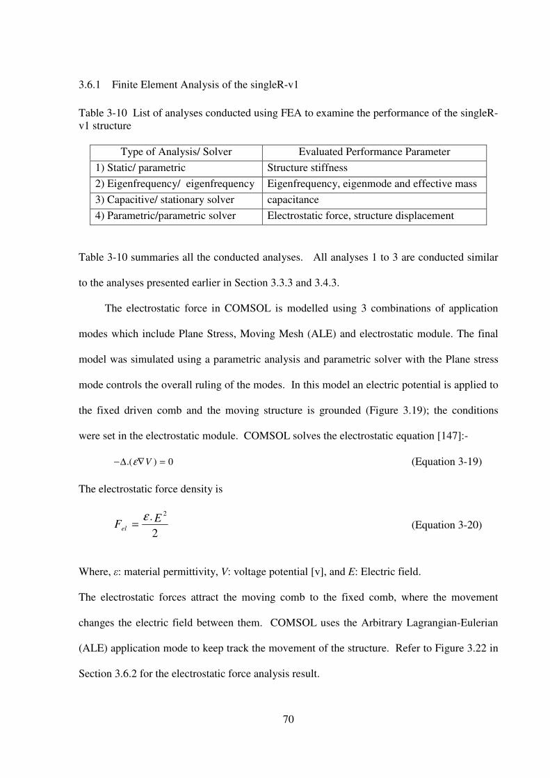
70
3.6.1 Finite Element Analysis of the singleR-v1
Table 3-10 List of analyses conducted using FEA to examine the performance of the singleR-
v1 structure
Type of Analysis/ Solver Evaluated Performance Parameter
1) Static/ parametric Structure stiffness
2) Eigenfrequency/ eigenfrequency Eigenfrequency, eigenmode and effective mass
3) Capacitive/ stationary solver capacitance
4) Parametric/parametric solver Electrostatic force, structure displacement
Table 3-10 summaries all the conducted analyses. All analyses 1 to 3 are conducted similar
to the analyses presented earlier in Section 3.3.3 and 3.4.3.
The electrostatic force in COMSOL is modelled using 3 combinations of application
modes which include Plane Stress, Moving Mesh (ALE) and electrostatic module. The final
model was simulated using a parametric analysis and parametric solver with the Plane stress
mode controls the overall ruling of the modes. In this model an electric potential is applied to
the fixed driven comb and the moving structure is grounded (Figure 3.19); the conditions
were set in the electrostatic module. COMSOL solves the electrostatic equation [147]:-
0).( =∇∆− Vε (Equation 3-19)
The electrostatic force density is
2
. 2E
Fel
ε= (Equation 3-20)
Where, ε: material permittivity, V: voltage potential [v], and E: Electric field.
The electrostatic forces attract the moving comb to the fixed comb, where the movement
changes the electric field between them. COMSOL uses the Arbitrary Lagrangian-Eulerian
(ALE) application mode to keep track the movement of the structure. Refer to Figure 3.22 in
Section 3.6.2 for the electrostatic force analysis result.

71
3.6.2 Performance of the SingleR-v1 Structure
Table 3-11 Performance parameter analysis result of the single fixed-fixed beam resonator
(SingleR-v1)
Performance Parameter of comb actuator Value
Structure stiffness ky [N/m] 5.234
Natural Frequency ωn[Hz] 22127.1
Effective mass, meff [kg] 2.708 x 10⁻¹⁰
Change of capacitance,dc/dy [F/µm] 2.09 x 10⁻¹⁵
Electrostatic force, Fel [N] (at 5 v voltage potential) 1.07 x 10⁻⁴
Generated current, iout [A] (assuming at 8 V sense voltage) 2.32 x 10⁻⁹
Figure 3.20 Fundamental eigenfrequency of the fixed-fixed beam resonator (SingleR-v1), (a)
3D view of structure analysis (x-y-z plane); (b) Top view (x-y plane)
Table 3-11 presents the overall performance of the SingleR-v1 Structure. By rigidly coupled
the beam to the driven and readout comb, the stiffness of the structure increases from 2.74
N/m (for single fixed-fixed beam only) to 5.234 N/m. From the eigenfrequency analysis
result (Figure 3.20) the fundamental eigenfrequency of the structure is 22127.1 Hz. In this
frequency mode, the comb actuator and the resonator move forward together in the y-
direction of movement. Equation 3-1 which relates the effective stiffness, mass and natural
frequency of the structure was used to calculate the effective mass of the singleR-v1 structure.
(a) (b)

72
Figure 3.21 Static capacitance and change of capacitance (dc/dy) of the SingleR-v1 structure
Figure 3.22 (a) Generated electrostatic force [N] at different voltage potential [v]; (b) Static
displacement due to the generated electrostatic force.
From the capacitance analysis result (Figure 3.21), with a 5µm initial overlapping structure
fingers, the static capacitance is approximately 2.12 x 10⁻¹⁴
F. With 5V potential differences
between the fixed and moving fingers, the structure generates 1.07 x 10⁻⁴
N electrostatic force
(Figure 3.22(a)), which causes 2.097 x 10⁻⁹
m structure movement (Figure 3.22 (b)). Due to
the comb movement and fluctuation of the capacitance, it generates a current around
2.32nanoA at the readout port. With the amount of the generated current, the response of the
Static Displacement of Comb
Actuator (due to Fel )
0
1E-08
2E-08
3E-08
4E-08
0 5 10 15 20
Voltage Potential [V]
Dis
pla
cem
ent [m
]
Electrostatic Force Analysis
Result
0.E+00
1.E-03
2.E-03
0 5 10 15 20
Voltage Potential, V [v]
Fel
, [
N]
(a) (b)
Capacitance Analysis Result: SingleR-MLA-v1
0.0E+00
2.0E-14
4.0E-14
6.0E-14
8.0E-14
0 5 10 15 20Overlapping Distance [µm]
Cap
acit
ance
C
dc/ dy

73
singleR-v1 Structure is expected to be measurable (refer to Chapter 6 and 7 for structure
fabrication and frequency response measurement result).
3.7 Summary and Conclusion
The coupled micro resonator array (CMRA) was designed and modelled so that it can be
fabricated (using in-house facilities) and the output signal can be measured using the available
readout measurement facilities. Therefore all the constraints of the expected output signal, the
measurement and fabrication were included in the design stage of the structure (Section 3.2).
The output signals of the CMRA which in the form of frequency response pattern of the
coupled structure are related to the effective mass and stiffness of the coupled elements. The
effectiveness of the CMRA-v1 relies on the functionality of the fixed-fixed beam resonator,
coupling stiffness of the butterfly spring to synchronize the motion of the resonators and the
comb actuator to drive and readout the output signal. The structure was designed to ensure no
unwanted coupling in between the five main eigenfrequencies of the structure.
The stiffness of the coupling spring affects the overall frequency response pattern of the
CMRA. From the finite element analysis result of the butterfly spring (Section 3.4.4),
increasing the coupling stiffness increases the peak to peak response bandwidth and the
overall bandwidth of the 5 ripples frequency response and decreases the amplitude of the
response. The frequency response of the CMRA is also affected by the damping condition
(viscous and acoustic damping). From finite element analysis of the single fixed-fixed beam
resonator, the increase of damping factors reduced the response amplitude of the output signal
and widened the bandwidth of the response.
A unique frequency response pattern for a single or multiple sensor is a key aspect of the
CMRA structure. As analysed and discussed in Section 3.4.5, the response of the first half of

74
the sensor structure of the symmetrical coupled fixed-fixed beam resonators are always
identical to the response of the second half of the structure when the structure absorbs similar
amount of mass. To enhance the uniqueness of the frequency response of the coupled
resonators for CMRA sensor structure, further analysis will be discussed in Chapter 4.
To ensure the output signal of the CMRA is measurable, at least 1nanoA of current
(iout) needs to be generated at the readout port of the comb actuator. The iout generation is
controlled by the change of the capacitance (dc/dy) and the flexibility of the readout comb
actuator to fluctuate in the y-direction of movement. From the numerical and finite element
analysis around 3nanoA current was estimated to be generated at the readout comb actuator.
Based on the generated current, the structure is expected to be measurable.
When the comb drive actuator was coupled to the resonator (R1), the actuator failed to
drive the CMRA structure. The large designed mass of the comb drive actuator (i.e. 53x
more than the mass of resonator) created a standalone node at the next resonator (R2). Hence,
it is important to further examine the mass of the 5 coupled resonators and the actuators to
ensure measurable output signals. The overall effect of the mass and stiffness of the CMRA
structure elements on the measurability of the output signal will be further analysed in
Chapter 4 using a lumped mass model analysis.
Although other methods of excitation and detection (e.g. piezoelectric excitation and
optical detection) may be used as an alternative to excite and readout the response of the 5
coupled fixed-fixed beam resonators; but, it is outside the research scope. To keep the
electrostatic excitation and the capacitive detection scheme to detect the response pattern of
the CMRA, the research improved the CMRA structure design by using an integrated coupled
comb-drive resonator as the main structure element of the second version of the CMRA (will
be discussed in Chapter 4 and Chapter 5).

75
CHAPTER 4 IMPROVEMENT OF CMRA USING LUMPED
MASS MODEL ANALYSIS
4.1 Introduction
This chapter evaluates and analyses the performance of the coupled micro resonator array
(CMRA) structure using the lumped mass model approach. Section 4.2 explains the overall
lumped mass model of the CMRA structure which is based on an eigenvalue and eigenvector
analysis. Section 4.3 briefly presents re-evaluation of the CMRA-v1 structure using the
lumped mass model. Section 4.4 examines two alternatives of the lumped mass CMRA
structures in order to improve the measurability of the CMRA structure output signal. To
establish the improved CMRA structures, Section 4.5 highlights keys design improvement of
the structure. Section 4.6 evaluates, and discusses the alternatives of the staggered lumped
mass CMRA structures in terms of the measurability of output signals, uniqueness of
frequency response patterns and stability of system eigenvectors. Section 4.7 summarizes the
overall achievement in Chapter 4.
4.2 Lumped Mass Model of CMRA
Figure 4.1 Schematic of the 5 CMRA-v1 sensor structures
Fixed-fixed beam resonator
Mechanical coupling spring
X5
Input
X1
K1
R1 R2
X2
R3 R5
X3 X4
M1
K2 K3 K4 K5
M2 M3 M4 M5
Readout port
Rigid coupling
Drive port
KC1 KC2 KC3 KC4 Output
R4
F1(t)

76
Figure 4.1, a schematic of the first version of the coupled micro resonator array (CMRA-v1)
which was discussed earlier in Chapter 3. The structure consists of 5 coupled resonators (R1,
R2, R3, R4, and R5), and 4 mechanical coupling springs to couple the resonators together. To
drive and readout the output signal of the structure, 2 sets of comb actuators were rigidly
coupled to both end of the resonators array.
To re-evaluate the structure performance using the lumped mass analysis, the CMRA-
v1 structure is considered as a five degrees-of-freedom (DOF) system. The structure is
represented by 5 coordinates to describe its motion; i.e. x1, x2, x3, x4, and x5. The 5-DOF
system has 5 natural frequencies; each natural frequency is characterized by a natural state of
vibration with a displacement configuration which is called normal mode [137, 148]. In
mathematics they are referred to eigenvalues and eigenvectors.
Figure 4.2 Free body diagram of the five CMRA structure
The relationship between eigenfrequencies and eigenvectors is established from the equations
of motion of the system. Referring to the coupled resonators in Figure 4.1, consider a free
body diagram of the system (Figure 4.2). The equations of motion of the system in Figure 4.2
are as follows:-
At M1:
XC ɺ11
X1 F1(t)
KC1 (X1- X2) K1X1 M1
X1 X2 X3 X4 X5
K1
C1
M1
K2
C2
M2
K3
C3
M3
K4
C4
M4
K5
C5
M5
KC1 KC2 KC3 KC4
F1(t)

77
FXKXKKXCXM CC 1211111111_ =
+++ ɺɺɺ
(Equation 4-1)
At M2:
XC ɺ
22
0
322212112222__ =
++++ XKXKKKXKXCXM CCCC
ɺɺɺ
(Equation 4-2)
At M3:
XC ɺ33
0
433323223333__ =
++++ XKXKKKXKXCXM CCCC
ɺɺɺ
(Equation 4-3)
At M4:
XC ɺ44
0
544434334444__ =
++++ XKXKKKXKXCXM CCCC
ɺɺɺ
(Equation 4-4)
At M5:
XC ɺ55
0545445555
_ =
+++ XKKXKXCXM CC
ɺɺɺ
(Equation 4-5)
K2X2
KC1 (X1- X2) M2
KC2 (X2- X3)
KC2 (X2 - X3)
K3X3 M3 KC3 (X3 - X4)
KC4 (X4 - X5) K4X4
M4 KC3 (X3 - X4)
K5X5 M5 KC4 (X4 – X5)

78
The above equations of motion (4-1 – 4-5) of the system are simplified in a matrix form as:
[ ] [ ] [ ]F
X
X
X
X
X
K
X
X
X
X
X
C
X
X
X
X
X
M
M
M
M
M
=
+
+
5
4
3
2
1
.
5
4
3
2
1
.
5
4
3
2
1
50000
04000
00300
00020
00001
.
ɺ
ɺ
ɺ
ɺ
ɺ
ɺɺ
ɺɺ
ɺɺ
ɺɺ
ɺɺ
(Equation 4-6)
Where, [ ]C is a damping matrix; [ ]K is a stiffness matrix; and [ ]F is a force matrix;
[ ]F =
0
0
0
0
1F
; [ ]C =
C
C
C
C
C
50000
04000
00300
00020
00001
;
[ ]K =
+−
−++−
−++−
−++−
−+
KCKKC
KCKCKCKKC
KCKCKCKKC
KCKCKCKKC
KCKCK
454000
4434300
0332320
0022121
000111
In order to determine the natural frequencies and modes shape of the CMRA, the above
system is examined under a free vibration and treated as an undamped system; where F1(t) = 0
and [C] = 0. The system in Figure 4.2 is simplified as follows:
Figure 4.3 Free body diagram of undamped CMRA structure
X1 X2 X3 X4 X5
M1 M2 M3 M4 M5
KC1 KC2 KC3 KC4
K1 K2 K3 K4 K5
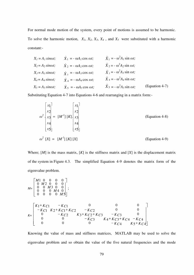
79
For normal mode motion of the system, every point of motions is assumed to be harmonic.
To solve the harmonic motion, X1, X2, X3, X4 , and X5 were substituted with a harmonic
constant:-
(Equation 4-7)
Substituting Equation 4-7 into Equations 4-6 and rearranging in a matrix form:-
ω2 =
x
x
x
x
x
5
4
3
2
1
. [M-1
] [K]
x
x
x
x
x
5
4
3
2
1
. (Equation 4-8)
ω2
[X] = [M-1
] [K] [X] (Equation 4-9)
Where; [M] is the mass matrix, [K] is the stiffness matrix and [X] is the displacement matrix
of the system in Figure 4.3. The simplified Equation 4-9 denotes the matrix form of the
eigenvalue problem.
M=
5000004000003000002000001
MM
MM
M
;
K=
+−−++−
−++−−++−
−+
K CKK C
K CK CK CKK C
K CK CK CKK C
K CK CK CKK C
K CK CK
4540004434300
0332320
0022121
000111
Knowing the value of mass and stiffness matrices, MATLAB may be used to solve the
eigenvalue problem and so obtain the value of the five natural frequencies and the mode
X5 = A5 sinωt; = - ωA5 cos ωt; Xɺ 5 Xɺɺ 5
= - ω2
A5 sin ωt;
X1 = A1 sinωt; = - ωA1 cos ωt; Xɺɺ 1
X2 = A2 sinωt; = - ωA2 cos ωt; Xɺ 2
Xɺɺ 2 = - ω2
A2 sin ωt;
= - ω2A1 sin ωt; Xɺ 1
X3 = A3 sinωt; = - ωA3 cos ωt;
X4 = A4 sinωt; = - ωA4 cos ωt; Xɺ 4 = - ω2
A4 sin ωt;
= - ω2A3 sin ωt;
Xɺ 3
Xɺɺ 3
Xɺɺ 4

80
shapes of the CMRA structure can be estimated. For example, using the MATLAB, the
eigenvalues and eigenvectors are determined using a function of [V, d] = eig(E). Where V
contains the eigenvectors, d contains the eigenvalues and E = [M-1
] [K] (refer to Appendix B
for the example of MATLAB codes).
4.3 Re-evaluation of the CMRA-v1
As discussed in Section 3.5.5 (Chapter 3), due to the very large mass of the actuator, the
actuator failed to drive the coupled resonators. As a result the readout comb actuator was
unable to detect the frequency response of the coupled resonators. To evaluate the
performance of the CMRA-v1 using the lumped mass model analysis, the value of the
effective mass, and stiffness of the resonators, comb actuators and coupling springs were
obtained from the finite element analysis in Section 3.3.4 (Table 3-2), Section 3.4.3 (Table 3-
4), and Section 3.5.4 (Table 3-9). Table 4-1 summarizes the effective mass and stiffness of
the CMRA-v1 structure elements.
Using MATLAB the value of the effective mass and stiffness of the CMRA-v1 structure
elements in Table 4-1 were substituted in Equation 4-9 in order to solve for the 5 eigenvalues
and 5 eigenvectors of the coupled structure. Figure 4.4 shows the plot of the 5 eigenvectors of
the CMRA-v1 structure for 5 structure eigenmodes.
The measurability of the structure output signal is associated with the absolute
movement of the structure (response amplitude) at the particular drive or readout point. As
can be observed at R1 (drive point) and R5 (readout point) the 2 large resonators displacement
(mode 1 and mode 2) are only associated to the movement of the large mass of the actuators
which was coupled to the structure array. For mode 3, 4, and 5 the resonators approach zero
displacement at both ends of the array. The large masses have created nodes between

81
actuators and resonators. As a result the output signal of the structure at R5 is unable to be
measured.
Table 4-1 A summary of the effective mass and stiffness of the CMRA-v1 structure elements
(Note: Kc1= Kc2= Kc3=Kc4= 0.4578N/m)
Structure Elements Effective Mass
Parameter [kg]
Effective Stiffness
Parameter [N/m]
Resonator 1 (R1) and
Driven comb actuator
M1: 1.5832 x 10⁻⁹
K1: 3.3255
Resonator 2 (R2) M2: 2.92 x 10⁻¹¹
K2: 2.74
Resonator 3 (R3) M3: 2.92 x 10⁻¹¹
K3: 2.74
Resonator 4 (R4) M4: 2.92 x 10⁻¹¹
K4: 2.74
Resonator 5 (R5) and
readout comb actuator
M5: 1.5832 x 10⁻⁹
K5: 3.3255
Figure 4.4 Eigenmode analysis result of CMRA-v1
4.4 Analysis of Improved Design
In order to ensure a measurable output signal of the structure (i.e. drive at R1, readout at R5),
the nodes at both end of the structure array need to be removed. The research explores several
alternative structures by modifying the mass and stiffness of the CMRA-v1 structure (in Table
4-1). Two alternatives are discussed:-
• Alternative 1: The original stiffness were retained, but the masses of the coupled
elements were changed, so that they are equivalent to M1 (Table 4-1).
Node
1 2 3 4 5-1
-0.5
0
0.5
1Eigenmode Analysis of CMRAv1
Resonator 1 to 5
Rel
ativ
e D
isp
lace
men
t
mode1
mode2
mode3
mode4
mode5
Node

82
• Alternative 2: The masses and stiffness of the coupled elements were changed, so that
they have similar masses (M1) and similar stiffness (K2).
Having resonators and actuators which have similar masses may balance the relative
displacement of the coupled structure. Hence, the node between the actuators and resonators
may be removed. Two alternatives were compared and the effect of the change of mass and
resonator stiffness on the structure eigenvalues and eigenvectors were observed. Table 4-2
summarizes the modification of the effective mass and stiffness of the 5 coupled elements for
the two structure alternatives. Note that the 4 coupling stiffness used to couple the 5 structure
elements remained 0.4578 N/m.
Table 4-2 Modified effective mass and stiffness of the 5 coupled structures for structure
improvement analysis
Effective mass, M and stiffness, K [N/m] of the 5
coupled elements Note: * (x 10-9
) [kg]
Alternative 1 Alternative 2
Structure
Elements
M K M K
1 1.5832* 3.3255 1.5832
* 2.74
2 1.5832* 2.74 1.5832
* 2.74
3 1.5832* 2.74 1.5832
* 2.74
4 1.5832* 2.74 1.5832
* 2.74
5 1.5832* 3.3255 1.5832
* 2.74
Using MATLAB, the lumped mass analyses were performed to determine the eigenvectors
and eigenfrequencies of the coupled structures based on the two alternatives mass and
stiffness parameters in Table 4-2. Figure 4.5 shows the plots of the eigenmodes analysis
result for each of the two alternatives. Table 4-3 lists the 5 eigenfrequencies of the uncoupled
structure and modal eigenfrequencies of the coupled structures for the two alternatives and
CMRA-v1. Table 4-4 highlights the normalized eigenvectors of the two structure alternatives
compared to the CMRA-v1.

83
Figure 4.5 Eigenmode analysis result of 2 alternatives structure improvement of CMRA-v1
Table 4-3 Eigenfrequencies (fR) and modal eigenfrequencies (fm) of the CMRA-v1 and
structure alternatives
CMRA-v1 Alternative1 Alternative2
fR fm fR fm fR fm
fR1, fm1
fR2, fm2
fR3, fm3
fR4, fm4
fR5, fm5
7294
48753
48753
48753
7294
7718
7720
51089
56321
61100
7294.3
6621.1
6621.1
6621.1
7294.3
6790.0
7219.0
7735.7
8179.5
8459.3
6621.1
6621.1
6621.1
6621.1
6621.1
6621.1
6829.1
7345.8
7938.2
8386.8
Table 4-4 Eigenvectors analysis result of the CMRA-v1 and structure alternatives
Normalized Eigenvectors ( of 5 coupled structure) Alternative
/Resonator (R) Mode1 Mode2 Mode3 Mode4 Mode5
CMRA-v1 R1
R2
R3
R4
R5
29.7
4
1
4
29.7
-7.8
-1
0
1
7.8
-1
356.9
505.4
356.9
-1
1
-415.9
0
415.9
-1
-1
500.2
706.9
500.2
-1
Alternative
1
R1
R2
R3
R4
R5
1
2
2.3
2
1
-1
-1.1
0
1.1
1
-10.6
-1
10.8
-1
-10.6
-1.1
1
0
-1
1.1
1
-1.5
1.7
-1.5
1
Alternative
2
R1
R2
R3
R4
R5
1
1
1
1
1
-1.6
-1
0
1
1.6
2.6
-1
-3.2
-1
2.6
-1
1.6
0
-1.6
1
1
-2.6
3.2
-2.6
1
1 2 3 4 5
-0.6
-0.4
-0.2
0
0.2
0.4
0.6
Structure Improvement - Alternative 2
Resonator 1 to 5
Rel
ativ
e D
isp
lace
men
t
[Arb
itra
ry U
nit
]
mode1
mode2
mode3
mode4
mode5
1 2 3 4 5
-0.6
-0.4
-0.2
0
0.2
0.4
0.6Structure Improvement - Alternative 1
Resonator 1 to 5
Rel
ativ
e D
isp
lace
men
t[A
rbit
rary
Un
it]
mode1
mode2
mode3
mode4
mode5
(a) (b)

84
For alternative 1 (Figure 4.5(a)), when the mass of the resonators are similar, the displacement
of the resonators drastically is improved at R1 and R5. As can be observed in Table 4-3 and
Table 4-4, by having small differences between the eigenfrequencies of the uncoupled
resonators, improved the relative displacement of the resonators. Although, the actual relative
displacement of the resonator depending on the mass and stiffness configuration of that
particular resonator.
Referring to alternative 2 (Figure 4.5(b) and Table 4-4), with the uniform mass and
stiffness configuration (similar eigenfrequencies for the 5 uncoupled elements), differences of
the proportion of the relative displacement between the 5 coupled resonators are small (i.e.
balanced relative displacement). Hence, no standalone node is created between the 5
resonators. Therefore, the measurability is confirmed at R1 and R5 for all the modes when the
structures are coupled together.
From the above analysis results, the measurability of the coupled resonators depends on
the eigenfrequencies, the mass and stiffness configuration of the uncoupled elements. A large
mass differences between the coupled elements will cause the standalone node at the
particular resonator. The large mass will reduce the relative displacement of the resonator,
and hence the responses of the resonators are unable to be measured at that particular
resonator. The mass and stiffness configuration of the resonators determined the range of the
modal frequencies of the coupled structures and the range of frequencies which dominate the
movement of the coupled structures.
Overall, the pattern or mode shape of the 5 coupled structures is directly related to the
eigenfrequencies of each uncoupled element (fR) and the eigenvectors of the coupled
resonators. Therefore, we may configure the mass or stiffness of the resonator in order to
control the eigenfrequencies of the coupled elements and modify the structure mass to control

85
the relative displacement (eigenvector) of the coupled structures. With the harmonization of
the relative displacement of the couple structures and the eigenfrequencies of the coupled
elements will determine the measurability of the output signal of the structure as well as the
final frequency response pattern of the coupled structures.
4.5 Key Structure Improvement of the CMRA-v2
4.5.1 Measurability of Output Signal
The measurability of the output signal of the CMRA sensor structure relies on the balanced
effective mass, stiffness of the coupled resonators, the mechanical coupling spring, and the
actuators. As discussed in Section 4.4, the measurability of the coupled structure is definitely
improved when the mass and stiffness of the resonators and actuators are similar (constant
mass and stiffness). The main design challenge is to alter the mass and stiffness of the
resonators and actuators, so that they are more or less similar. The mass modification needs
to be configured without compromising the amount of capacitance generated in the system
(for the readout measurement).
4.5.2 Unique Frequency Response Pattern
As discussed in Chapter 3 (Section 3.2.2.1) a unique frequency response pattern is important
as a signature to identify which single or multiple resonators absorbs mass. As analysed in
Section 3.4.5, with the symmetrical CMRA design (constant mass coupled resonators), the
structure does not have a unique frequency response pattern for individual resonator mass
changes. The frequency response pattern of the individual resonator in the first half of the
array are always similar to the resonators in the second half of the array, when the resonator
absorbs similar amount of mass separately (i.e. the response pattern of R1 mirrors R5 and R2
mirrors R4).

86
Since the mass and stiffness of the coupled structures control the modal eigenfrequencies of
the resonator, the symmetrical mass and stiffness configuration of the 5 resonators may be
broke (e.g. staggering the resonators mass) for a distinguishable frequency response pattern.
However, it is very important to consider, the degree to which the 5 resonators are staggered.
The staggered mass must not create a large change between the proportion of the relative
displacements of the 5 coupled structures; a large difference between the 5 eigenvectors, will
increase risk that the response of some of the resonators with low relative displacement will
not be measurable.
4.5.3 Stability of Eigenvectors
An eigenvector describes the relative displacement of any point on the structure as the
structure vibrates in a single mode [136]. When one of the resonators of the CMRA absorbs a
mass, the change of the mass may be identified by using an inverse eigenvalue analysis. This
requires knowledge of the perturbed eigenvalues (eigenfrequency after the structure absorbs
the mass) and perturbed eigenvectors. Since the perturbed eigenvectors are complicated to
measure, the unperturbed eigenvectors will be used in the estimation of the mass changes
pattern of the CMRA. To reduce errors in mass estimation, it is important to ensure that the
eigenvectors are stable against mass changes (i.e. comparable eigenvectors or comparable
eigenmodes before and after mass is absorbed).
4.6 Lumped Mass Model of the CMRA-v2 and Structural Analysis
4.6.1 CMRA-v2 for Measurability of Output Signal
To ensure measurable frequency responses, the research considers a new configuration of the
CMRA structure based on the integrated coupled comb-drive resonators (Figure 4.6). The use

87
of the comb-drive to replace the fixed-fixed beams resonators and simultaneously acts as
actuators will solve the problem of large mass differences between the actuators and
resonators and ensure sufficient electrostatic forces and capacitances for the drive and readout
requirement.
The new CMRA structure with balanced mass configurations between the resonators and
actuators (i.e. constant mass and stiffness) will help to ensure measurability of the CMRA
frequency response.
Figure 4.6 The schematic of the improved version of CMRA-v2 structure
4.6.2 Breaking Structure Symmetry for Performance Improvement of CMRA
Six alternatives were analysed in order to determine effective ways to stagger the coupled
resonators; so that the structure is measurable, produces a unique frequency response, has
stable eigenvectors before and after mass is perturbed at each of the single resonator.
• Alternative(1) and Alternative(2): 0.1 and 1 percent uniform step staggered mass of 5
CMRA respectively. The analyses examine the effect of 0.5% and 5% total staggered
mass on the change of the eigenvectors of the 5 resonators. Note that a larger stagger
(more than 1%) may result in a reduced measurability of the output; any smaller less
than 0.1% causes the absorbed mass or manufacturing variations would dominate.
Comb-drive resonator Mechanical coupling spring
X4 X1 X2 X3 X5
KC1 KC2 KC3 KC4
R1 R2 R4 R5 R3
K1 K2 K3 K4 K5 M1 M2 M3 M4 M5

88
• Alternative(3) and Alternative(4): An unsymmetrical, but balanced mass distribution
between the first half and second half of the structure array (sum of R1 and R2 mass is
equal to the sum of mass of R4 and R5). With the unsymmetrical but balanced mass
distribution approach, the amount of the total staggered mass may be increased without
reducing the measurability of the structure output signal. The analyses compare the
effect of 7% total staggered mass on the change of the eigenvectors when the heaviest
mass is positioned in the middle (Alternative(3)) and at both ends of the structure array
(Alternative(4)). Positioning the heaviest mass at the middle of the structure array may
help to effectively balance the relative displacement of the coupled resonators for
measurable output signal; constraining the heaviest mass at the end of the structure
array may help to stabilize the eigenmodes of the perturbed CMRA.
• Alternative(5): Unsymmetrical, but balanced stiffness distribution between the first half
and second half of the structure array (K1 + K2 is equal K4 + K5). The most stiff
resonator is positioned in the middle of the array (R3).
• Alternative(6): 0.1 percent step staggered stiffness of 5 CMRA.
Table 4-5 lists the details of mass and stiffness configuration of the alternative structures. The
mass (M) and stiffness (K) value of resonators is based on a comb-drive resonator from a
group research project, which was designed by Anthony [125, 149]. The mass and stiffness
of the resonators are evaluated using finite element analysis, which are discussed in Chapter
5. Note that the four coupling constants for all the structure alternatives is 0.3118 N/m.

89
Table 4-5 Mass and stiffness configurations of 6 alternatives of the staggered CMRA
Effective mass, M and stiffness, K of the 5 coupled elements
Note: M =3.8267nanokg; K = 24.9741N/m
Alternative(1) Alternative(2) Alternative(3)
Coupled
Resonators
M K M K M K
R1 M + 0.1%M K M + 1%M K M - 4%M K
R2 M + 0.2%M K M + 2%M K M - 1%M K
R3 M + 0.3%M K M + 3%M K M K
R4 M + 0.4%M K M + 4%M K M - 2%M K
R5 M + 0.5%M K M + 5%M K M - 3%M K
Alternative(4) Alternative(5) Alternative(6)
M K M K M K
R1 M + 4%M K M K - 4%K M K + 0.1%K
R2 M + 1%M K M K - 1%K M K + 0.2%K
R3 M K M K M K + 0.3%K
R4 M + 2%M K M K - 2%K M K + 0.4%K
R5 M + 3%M K M K - 3%K M K + 0.5%K
As discussed in Section 4.3 and 4.4, the lumped mass analysis of the CMRA was performed
using MATLAB programming. By substituting the value of mass and stiffness of the
structures in Equation 4-9, the analysis returns the value of 5 eigenfrequencies and 5
eigenvectors of the coupled structure. The measurability of the structure output signal is
determined by observing the eigenvectors of the structure alternatives at R1 and R5. Once the
measurability of the structure output signal is confirmed, the eigenvalue and eigenvector
analysis is repeated to examine the uniqueness of frequency response pattern and the stability
of system eigenvectors.
A series of five tests were performed where a mass of 3.8267 x 10⁻¹²
kg (~0.1%) was
added to R1, R2, R3, R4 and R5 separately. The eigenfrequencies and the eigenvectors of the
unperturbed structure (i.e. initial condition) and perturbed structure (after the mass was added)
were observed and compared. The stability of the eigenvectors of the CMRA with the
constant mass (M1 = M2 = M3 = M4 = M5 = M =3.8267nanokg) and constant stiffness (K1 =

90
K2 = K3 = K4 = K5 = K = 24.9741N/m) was also analysed by adding the same amount of
mass to R1, R2 , R3, R4, and R5 separately.
4.6.3 Result and Discussion
Figure 4.7 Eigenmode analysis result of 6 alternatives of Staggered CMRA
Figure 4.7 shows the eigenmodes analysis result of the 6 alternatives of the staggered CMRA.
If we observe the eigenvectors at resonator 1 (R1) and R5 only 3 structure alternatives, (a):
1 2 3 4 5-0.8-0.6-0.4-0.2
00.20.40.60.8
Eigenmode Analysis Result - Alternative 2
Resonator 1 to 5
Eig
env
ecto
rs
mode1
mode2
mode3
mode4
mode5
(b)
1 2 3 4 5-0.8-0.6-0.4-0.2
00.20.40.60.8
1
Eigenmode Analysis Result - Alternative 4
Resonator 1 to 5
Eig
env
ecto
rs
mode1
mode2
mode3
mode4
mode5
(d)
1 2 3 4 5-0.8-0.6-0.4-0.2
00.20.40.60.8
1
Eigenmode Analysis Result - Alternative 5
Resonator 1 to 5
Eig
env
ecto
rs
mode1
mode2
mode3
mode4
mode5
(e)
1 2 3 4 55-0.8-0.6-0.4-0.2
00.20.40.60.8
Eigenmode Analysis Result -
Alternative 1
Resonator 1 to 5
Eig
env
ecto
rs
mode1
mode2
mode3
mode4
mode5
(a)
√√√√
1 2 3 4 5-0.8-0.6-0.4-0.2
00.20.40.60.8
Eigenmode Analysis Result
- Alternative 3
Resonator 1 to 5
Eig
env
ecto
rs
mode1
mode2
mode3
mode4
mode5
(c)
√√√√
1 2 3 4 5-0.8-0.6-0.4-0.2
00.20.40.60.8
Eigenmode Analysis Result - Alternative 6
Resonator 1 to 5
Eig
env
ecto
rs
mode1
mode2
mode3
mode4
mode5
(f)
√√√√

91
Alternative(1), (c):Alternative(3), and (f):Alternative(6) (with ‘√’ mark on Figure 4.7) are
considered measurable since they all have an anti-node at the ends of the array.
Referring to alternative(1) (Figure 4.7(a)) and alternative(2) (b) with the uniform step-
staggered mass approach; at a small amount of staggered mass (i.e. 0.1%*M step increments)
all the 5 eigenmodes are measurable. However, with a slightly larger amount of the step-
staggered mass (i.e. 1%*M increment), the mode 1 and 5 (Figure 4.7 (b)) approached zero.
Therefore, mode 1 and 5 for alternative(2) expected unable to be measured.
Consider alternative(3) ((Figure 4.7(c)) and alternative(4) (Figure 4.7(d)) with the
unsymmetrical but balanced mass distribution between the first half and the second half of the
structure array. At a maximum of 7% total staggered mass on the structure array and with the
heaviest mass positioned in the middle, all the 5 modal frequencies of the structure are
measurable at R1 and R5. Positioning the heaviest mass at the end of the array (R1 and R5),
(Figure 4.7 (d)) reduces the measurability of the structure output signal since the eigenvectors
of the structure at R1 and R5 restrained to zero.
For alternative(5) (Figure 4.7(e)) and alternative(6) (Figure 4.7(f)), where the structure
stiffness were staggered; with the unsymmetrical but balanced stiffness distribution for the
alternative(5), placing the most stiff resonator at the middle of array (R3) and the least stiff
resonator at the end of the array caused ineffective resonator displacement at R1 and R5.
Hence, most of the eigenmodes at R1 and R5 approached zero. For alternative 6, with small
uniform step-staggered stiffness (0.1%*K) all the structure eigenmodes at R1 and R5 are
measurable.
For the uniqueness of the frequency response pattern, consider the 5 modal frequencies
of the staggered structure in Table 4-6, when the 5 resonators absorbs a mass separately.
Comparing the 5 tests; although, some of the 5 modal frequencies of the structure alternatives

92
were identical when the single resonator (R1, R2, R3, R4 and R5) absorbs a mass (3.8267 x
10-12
kg) separately, but none of the test results completely mirror each other. Hence, it can
be claimed that by breaking the structure symmetry using the staggered mass or staggered
stiffness approaches (as exemplified by alternative(1), (3), and (6)) a unique frequency
response pattern can be produced for a single resonator mass changes.
Table 4-6 Eigenfrequency analysis result of the staggered CMRA (Alternative(1), (3), and
(6)); Note: identical colour for each structure alternative highlights similar eigenfrequencies
value
Modal Eigenfrequencies (fM) [Hz] Alternative of 5
CMRA Initial
+m
@R1
(Test 1)
+m
@R2
(Test 2)
+m
@R3
(Test 3)
+m
@R4
(Test 4)
+m
@R5
(Test 5)
fM1 12836 12835 12835 12834 12834 12833
fM2 12871 12868 12869 12870 12870 12869
fM3 12949 12947 12949 12946 12948 12947
fM4 13046 13045 13044 13046 13044 13045
fM5 13125 13125 13123 13123 13124 13125
Alternative
1
fM1 12932 12932 12930 12928 12931 12932
fM2 13054 13053 13051 13054 13052 13052
fM3 13111 13110 13109 13109 13110 13108
fM4 13234 13232 13234 13234 13232 13233
fM5 13256 13253 13255 13256 13255 13256
Alternative
3
fM1 12874 12872 12872 12873 12873 12874
fM2 12909 12908 12909 12909 12908 12906
fM3 12987 12986 12987 12985 12987 12985
fM4 13085 13084 13082 13085 13083 13084
Alternative
6
fM5 13164 13164 13162 13161 13162 13164
Figure 4.8 exemplifies the stability analysis result of structure eigenvectors for mode 2, before
and after mass was added to the single resonator separately (refer to Appendix C for a
complete eigenvectors stability analysis result for alternatives 1 to 6).

93
Figure 4.8 Stability of eigenvectors analysis result: example for mode 2; (a)-(f) six staggered
structure alternatives; (g) constant mass and stiffness CMRA
1 2 3 4 5-0.8
-0.6-0.4
-0.20
0.20.40.6
Stability of Eigenvectors (mode2)-
Alternative 1
Resonator 1 to 5
Eig
envect
ors
Initial
+m@R1
+m@R2
+m@R3
+m@R4
+m@R5
1 2 3 4 5
-0.6-0.4-0.2
00.20.40.60.8
Stability of Eigenvectors (mode2)-
Alternative 2
Resonator 1 to 5
Eig
envec
tors
Initial
+m@R1
+m@R2
+m@R3
+m@R4
+m@R5
1 2 3 4 5-0.8
-0.6
-0.4
-0.2
0
0.2
0.4
0.6
Stability of Eigenvectors (mode2)-
Alternative 3
Resonator 1 to 5
Eig
envec
tors
Initial
+m@R1
+m@R2
+m@R3
+m@R4
+m@R5
1 2 3 4 5
0
0.2
0.4
0.6
0.8
Stability of Eigenvectors(mode2)-
Alternative 4
Resonator 1 to 5
Eig
envec
tors
Initial
+m@R1
+m@R2
+m@R3
+m@R4
+m@R5
1 2 3 4 5-0.8-0.6-0.4-0.2
00.20.40.60.8
1
Stability of Eigenvectors (mode2)-
Alternative 5
Resonator 1 to 5
Eig
envec
tors
Initial
+m@R1
+m@R2
+m@R3
+m@R4
+m@R5
1 2 3 4 5
-1
0
1
Stability of Eigenvectors(mode2)-
Alternative6
Resonator 1 to 5
Eig
envec
tors
Initial
+m@R1
+m@R2
+m@R3
+m@R4
+m@R5
(a) (b)
(c) (d)
(e) (f)
1 2 3 4 5-0.8-0.6-0.4-0.2
00.20.40.60.8
Stability of Eigenvectors (mode2)-
Constant Mass & Stiffness CMRA
Resonator 1 to 5
Eig
env
ecto
rs
Initial
+m@R1
+m@R2
+m@R3
+m@R4
+m@R5
(g)

94
Consider alternative(1) and (2) (Figure 4.8(a), (b) and Appendix C); by uniformly staggering
the mass all the perturbed eigenvectors are stable (i.e. comparable eigenmodes) compared to
the unperturbed eigenvectors.
For alternative(3) and (4) (unsymmetrical staggered mass - balanced mass distribution
between the first and second half of the structure array), when the heaviest mass was
positioned in the middle of the structure array (Figure 4.8(c), Appendix C) all the perturbed
eigenvectors are stable except when mass is added at R1 (for mode 1 and mode 5). However
when the heaviest masses were restrained at both ends of the structure array (Figure 4.8(d),
Appendix C) all the perturbed eigenvectors are stable compared to unperturbed eigenvectors.
Hence, it can be claimed that by constraining the relative displacement of the end resonator
(i.e. positioning the heaviest mass at the end of the structure array) helped to stabilize the
structure eigenvectors.
When the structure stiffness was staggered (i.e. for Alternative(5) and (6); Figure 4.8(e),
and (f)); all the perturbed eigenvectors are unstable. Hence, it can be argued that, by only
staggering the stiffness of the resonators, we are unable to stabilize the perturbed
eigenvectors. Figure 4.8(g) depicts the stability of eigenvectors analysis result of 5 constant
mass and constant stiffness coupled resonators. With the constant mass resonators all the
perturbed eigenvectors are always different (unstable) compared to the unperturbed
eigenvectors.
From the overall analyses result, the staggered mass and staggered stiffness approaches
helped to break the structure symmetry of the 5 constant CMRA. As a result the structure
(Alternatives 1, 3, and 6) produced unique modal frequencies for the single resonator mass
changes.

95
The approach used to stagger the structure is very important to ensure a measurable output
signal and stable eigenvectors. Although, the uniform step staggered mass produced stable
eigenvectors, but at maximum of 1% staggered mass between each resonator the eigenvectors
at R1 and R5 for mode 1 and 5 approached zero. The Alternative(3) with the unsymmetrical
staggered mass but with balance mass distribution between the first half and second half of
the structure array (heaviest mass in the middle) is considered an effective way to stagger the
mass. At 7% total staggered mass (i.e. between R1 and R2, R1//R2: 3%, R2//R3:1%,
R3//R4:2%, and R4//R5:1%) the eigenvectors at R1, R2, R3, R4 and R5 are measurable for all
the 5 structure eigenmodes. Although, the eigenvectors were slightly unstable when mass was
added at R1, but the perturbed eigenvectors were stable for the other 4 single resonator mass
changes. Positioning the heaviest mass at the end of the structure array stabilized the
eigenvectors for all the 5 resonator mass changes; but some of eigenvectors at R5 (mode 1
and mode 5) reduced to zero.
Staggering only the resonator stiffness, did not stabilize the eigenvectors of the
perturbed structure. However, when we refer to the actual CMRA design, either by staggering
the mass or stiffness of the resonator, we in fact change the mass of resonators. Hence both
alternatives are used to stagger the CMRA (will be discussed in Chapter 5).
4.7 Summary and Conclusion
This chapter discusses the performance improvement of the CMRA using the lumped mass
model analysis. Re-evaluation of the CMRA-v1 in Section 4.3 confirmed that the two large
mass of the comb actuators which were rigidly coupled to R1 and R5 caused the standalone
node at R1 and R5. The large mass of the comb drive actuator restrained the displacement of
the R1 and R5. As a result, no movement was made to pull the adjacent resonators and the

96
readout comb actuator. Hence, the frequency response of the 5 coupled resonators is unable to
be measured at R5.
From the structure improvement analysis in Section 4.4, the measurability of the
structure output signal relies on the modal eigenfrequencies of the coupled structure and
system eigenvectors. The modal frequency and the eigenvectors depend on the fundamental
frequencies of the coupled structure, which was directly related to the mass and stiffness
configuration of the resonators. The eigenvectors of the structure which are controlled by the
configuration of the mass and resonator stiffness determined the final measurability of the
structure at a specific measurement point. With constant mass and constant stiffness
resonators the measurability of the 5 eigenmodes at R1 or R5 are confirmed. However, only
half of the single resonator sensor structure produced unique frequency response pattern; and
the perturbed eigenvectors for all single resonator mass changes were always unstable
compared to the unperturbed eigenvectors.
The main challenge of the CMRA-v2 is to ensure the structure is measurable, having a
unique frequency response pattern and stable perturbed eigenvectors compared to the
unperturbed structure. The unique frequency response pattern is very important in order to
detect the species absorbed by the resonator. The stable perturbed eigenvectors is important if
the unperturbed eigenvectors will be used to estimate the mass changes pattern absorb by the
resonators using the inverse eigenvalue analysis (will be discussed in Chapter 5).
Section 4.6 analyses and discusses few alternatives to break the structure symmetry of
the constant CMRA in order to produce a unique frequency response pattern, stabilize the
system eigenvectors and ensure the measurability of the structure output signal. Staggering
the mass or stiffness of resonators produced unique frequency response patterns. To ensure
the measurability of the coupled structure, the approach to stagger the structure and the

97
amount of the staggered mass is important. For example, the amount of the staggered mass
for the uniform step staggered mass alternative must be less than 1%*M in order to ensure a
measurable output signal of the 5 CMRA eigenmodes at both ends of the structure array. The
research finally selects the alternative(3) as the basis to stagger the mass and stiffness of the 5
constant mass CMRA in Chapter 5. With the 7% total staggered mass for 5 resonators and
the heaviest mass positioned in the middle of the structure array, the alternative(3) maintained
the measurability of the CMRA structure.

98
CHAPTER 5 - MODELLING, FINITE ELEMENT ANALYSIS
AND PERFORMANCE EVALUATION OF CMRA-V2
5.1 Introduction
This chapter presents an improved design of the coupled micro resonator array (CMRA-v2).
The designs of the CMRA-v2 include a Constant CMRA, a Staggered Mass and a Staggered
Stiffness CMRA are briefly explained in Section 5.2. Using COMSOL Multiphysics Finite
Element Analysis (FEA), the performance of the structure is analysed and discussed in
Section 5.3. Using a lumped mass model, Section 5.4 compares the performance of the
designed structures in terms of the measurability of the output signal, uniqueness of frequency
response pattern and stability of system eigenvectors. To further evaluate the stability of the
system eigenvectors, Section 5.5 presents an inverse eigenvalue analysis; the mass change
pattern of the CMRA-v2 single resonator sensor is estimated using the unperturbed design
eigenvectors and the evaluated perturbed eigenfrequencies from the eigenvalue and
eigenvectors derived for the perturbed structure in Section 5.4. This chapter also discusses the
research work related to the manufacturing variation analysis. Section 5.6 presents an
approach to quantify the manufacturing variation, discusses the result of the quantified data
and presents an analysis of the impact of manufacturing variation on the designed Constant
Mass CMRA.
5.2 Improved Design of CMRA-v2
This section presents the improved design of the CMRA-v2 structure which includes:-
• 5 Constant Mass CMRA
• 5 Staggered Mass
• 5 Staggered Stiffness CMRA

99
As discussed in Chapter 4, the Constant Mass CMRA design always produces a measurable
frequency response for all the 5 eigenmodes of the structure. However, the structure does not
produce a unique frequency response pattern for a single resonator mass perturbations and the
perturbed structure eigenvectors are always unstable (dissimilar) compared to unperturbed
eigenvectors. The 5 Constant Mass CMRA was designed in order to study and examine how
the manufacturing variation may naturally stagger the stiffness or mass of the coupled
resonators, and hence the final frequency response pattern of the structure.
As discussed in Section 4.6 (Chapter 4), with the staggered mass and staggered stiffness
approaches, a unique frequency response pattern was produced. With the staggered mass
approach the system eigenvectors of the CMRA was stabilized. Since the eigenvectors were
stabilized against the perturbation mass, the staggered stiffness approach alone could not
stabilize the eigenvectors. However, in reality when we stagger the stiffness of the resonator
(i.e. increasing or decreasing the length of resonator anchor spring) we actually stagger the
mass as well. Hence two approaches of the staggered mass (i.e. staggering linked masses of
the resonators, Section 5.2.2) and staggered stiffness (i.e. staggering the length of the anchor
spring) were chosen to improve the performance of the CMRA.
5.2.1 Five Constant Mass CMRA
Figure 5.1 shows the schematic of the second version of the 5 constant coupled micro
resonator array structure. The 5 Constant Mass CMRA consists of 5 constant mass comb-
drive resonators which were coupled with a narrowed S-shape or zigzag coupling spring.
Each single resonator is anchored with 4 semi zigzag anchor spring. The zigzag spring was
selected instead of butterfly spring to reduce the space occupied by the coupling spring. As
discussed in Section 3.4.1 the spurious responses introduced by the spring were reduced by
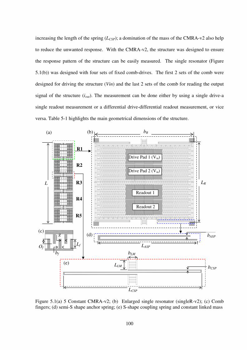
100
increasing the length of the spring (LCSP); a domination of the mass of the CMRA-v2 also help
to reduce the unwanted response. With the CMRA-v2, the structure was designed to ensure
the response pattern of the structure can be easily measured. The single resonator (Figure
5.1(b)) was designed with four sets of fixed comb-drives. The first 2 sets of the comb were
designed for driving the structure (Vin) and the last 2 sets of the comb for reading the output
signal of the structure (iout). The measurement can be done either by using a single drive-a
single readout measurement or a differential drive-differential readout measurement, or vice
versa. Table 5-1 highlights the main geometrical dimensions of the structure.
Figure 5.1(a) 5 Constant CMRA-v2; (b) Enlarged single resonator (singleR-v2); (c) Comb
fingers; (d) semi-S shape anchor spring; (e) S-shape coupling spring and constant linked mass
(c)
Lf
bf
g
Of
(d)
LASP
bASP
(b) bR
LR
Drive Pad 1 (Vin)
Drive Pad 2 (Vin)
Readout 1
Readout 2
(a)
L
R1
R2
R3
R4
R5
LCSP
bCSP (e) LLM
bLM

101
Table 5-1 Main geometrical design parameter of the 5 Constant CMRA
No.
Design
Parameter
Description of Geometrical
Comb Resonator Parameter
Dimension
[µm]
1 Length of Single R, LR 517
2 Width of Single R, bR 645
3 Length of 5 Constant CMRA, L 2818
4 Length of anchor spring, LASP 216
5 Width of anchor spring, bASP 3
6 Length of coupling spring, LCSP 575
7 Width of coupling spring, bCSP 3
8 Length of Linked mass, LLM 35
9 Width of Linked mass, bLM 39
10 Length of comb finger, Lf 10
11 Width of comb finger, bf 3
12 Gap between finger, g 3
13 Overlapping distance, Of 5
14 Total number of fingers, n 5260 fingers
5.2.2 Five Staggered Coupled Micro Resonator Array (Staggered CMRA)
In order to improve the performance of the CMRA, this research proposes 2 design
alternatives of the Staggered CMRA: (1) 5 Staggered Mass CMRA and (2) 5 Staggered
Stiffness CMRA. As discussed in Section 4.6, by breaking the symmetry of the structure,
both alternatives improved the distinguishability of the frequency response pattern of the
CMRA. Either the staggered mass (i.e. modifying the resonator linked mass) or the staggered
stiffness design alternatives (i.e. modifying length of the resonator anchor spring), the mass of
the coupled resonators are modified. Hence both alternatives are used to stabilize the system
eigenvectors.
For the 5 Staggered Mass CMRA, the main geometrical dimensions of the structure
were the same as the 5 Constant CMRA, except for the width of the linked mass (bLM, Figure
5.2(d)) which was used to connect the resonator and the coupling spring (design parameter no
9, Table 5-1). Figure 5.2 illustrates the schematic of the 5 Staggered Mass CMRA.

102
Figure 5.2 (a) Resonator 1, R1 (highlighted linked mass 1, LM1); (b) Schematic of Staggered
Mass CMRA; (c) R5; (d) Coupling 1- linked mass 1 and 2; (e) Coupling 2- linked mass 2 and
3; (f) Coupling 3- linked mass 3 and 4; (g) Coupling 4- linked mass 4 and 5
Coupling 1
Coupling 2
Coupling 3
Coupling 4
R1
R2
R3
R4
R5
(b)
(a)
(c)
Linked mass 1, LM1
bLM1 LLM1
Coupling 1 (d)
bLM2 LLM2
(e) Coupling 2
(f) Coupling 3
(g) Coupling 4

103
To break the symmetry of the constant CMRA, the Staggered Mass CMRA was designed with
a slight unsymmetrical mass distribution between all resonators. As discussed in Chapter 4, to
ensure the structure vibrates efficiently generating a measurable output signal, all masses in
the first half of the structure array (sum of R1 and R2) and the second half of the array (sum
of R4 and R5) remained balanced with the heaviest mass positioned in the middle of the
structure. The approach will help to effectively stagger the resonator mass and balance the
relative displacement of the 5 resonators for measurability of the structure output signal (i.e.
at R1 and R5). The length (LLM) of the linked mass for all resonators remained 35µm (Figure
5.2(d) – (g)). The width (bLM) of the linked mass for R1, R2, R3 and R5 were designed to be
39µm, 100, 119, 82, and 61µm respectively.
For the second alternative of the 5 Staggered Stiffness CMRA, the stiffness of the
resonators was varied by modifying the length (LASP) of the 4 anchor springs for each
resonator design parameter no.4, from Table 5-1. The least stiff resonator was positioned in
the middle of the coupled structure and the stiffer resonator at the end of the structure array.
Positioning the least stiff resonator which has the heaviest resonator mass (i.e. the longest
anchor spring) at the middle of the structure will help to ensure effective structure movement
for measurability of the output signal. The anchor spring length of the least stiff resonator R3
remained at 216µm and the other anchor springs for R1, R2, R4 and R5 were modified to
214.5µm, 215, 215.5 and 214µm respectively. All other geometrical design parameters
remained the same as the 5 Constant CMRA.
5.3 Modelling and Finite Element Analysis (FEA) of CMRA-v2
FEA using COMSOL Multiphysics was used to determine the performance of the designed
CMRA, i.e. the fundamental frequencies, the structure eigenmodes, the effective mass and

104
effective stiffness of the resonators, the capacitance generated by the comb-drive resonator
and the frequency response of the unperturbed CMRA.
5.3.1 Eigenfrequency and Eigenmode
To determine the fundamental frequency and the eigenmodes of the structure, an
eigenfrequency analysis was performed in the Plane Stress application mode of the COMSOL
FEA using the eigenfrequency solver. Table 5-2 lists the fundamental frequency of the
analysed CMRA structure.
Table 5-2 the eigenfrequency of comb-drive resonator (SingleR-v2) and fundamental modal
frequencies of the three designed CMRA(s) analysed using the FEA
Modal Eigenfrequencies [Hz] of the CMRA-v2 Frequency of
SingleR-v2
[Hz] 5 Constant Mass
CMRA
5 Staggered Mass
CMRA
5 Staggered Stiffness
CMRA
fM1 = 12543.5 fM1 = 12340.2 fM1 = 12574.8
fM2 = 12651.4 fM2 = 12502.2 fM2 = 12725.6
fM3 = 12792.2 fM3 = 12638.2 fM3 = 12874.5
fM4 = 12922.6 fM4 = 12806.1 fM4 = 13032.2
12857.3
fM5 = 13009.5 fM5 = 12848.2 fM5 = 13076.8
As can be seen in Table 5-2, all of the devices have fundamental frequencies centred around
12000 Hz. Comparing the five eigenfrequencies of the 5 Staggered Mass CMRA are slightly
lower than the 5 Constant CMRA, due to the extra mass. While, the 5 eigenfrequencies of the
Staggered Stiffness CMRA were slightly higher compared to the 5 Constant Mass CMRA,
this was due to the stiffer springs which were designed to anchor the structure.
Figure 5.3, 5.4 and 5.5 show the 5 eigenmodes of the CMRA structure for the 5
Constant CMRA, 5 Staggered Mass CMRA and 5 Staggered Stiffness CMRA respectively.
The 5 eigenmodes of the structure represent the relative movement of the coupled resonators
either in phase or anti-phase. The relative displacement values are summarized and tabulated
in Table 5-3, 5-4, and 5-5 respectively.

105
Figure 5.3 Eigenmodes analyses of 5 Constant Mass CMRA : (a) mode1; (b) mode2; (c)
mode3; (d) mode4; (e) mode5
Table 5-3 the relative displacement of the resonators (associated to different colour shown on
a scale bar ) from the eigenmode analysis of 5 Constant Mass CMRA (in Figure 5.3)
Mode 1
(a)
Mode 2
(b)
Mode 3
(c)
Mode 4
(d)
Mode 5
(e)
R1 +0.81 +1.48 +1.86 -1.76 +1.09
R2 +1.63 +1.74 +0.21 +1.47 -1.58
R3 +1.94 0 -1.88 0 +1.76
R4 +1.63 -1.74 +0.21 -1.47 -1.58
R5 +0.81 -1.48 +1.86 +1.76 +1.09
Figure 5.4 Eigenmodes analysis result of 5 Staggered Mass CMRA: (a) mode1; (b) mode2;
(c) mode3; (d) mode 4; (e) mode5
(e)
(d)
(c)
(b)
(a)
(a)
(b)
0
(c)
(d)
0
(e)

106
Table 5-4 the relative displacement of the resonators (associated to different colour shown on
a scale bar ) from the eigenmode analysis of 5 Staggered Mass CMRA (Figure 5.4)
Mode 1
(a)
Mode 2
(b)
Mode 3
(c)
Mode 4
(d)
Mode 5
(e)
R1 +0.54 -1.06 +1.34 +1.82 +2.06
R2 +1.66 -1.93 +1.07 -0.75 -1.46
R3 +2.27 +0.20 -1.93 -0.37 +1.10
R4 +1.36 +1.95 +0.79 +1.58 -1.27
R5 +0.50 +1.33 +1.79 -2.02 +1.18
Figure 5.5 Eigenmodes analysis result of 5 Staggered Stiffness CMRA: (a) mode1; (b)
mode2; (c) mode3; (d) mode 4; (e) mode5
Table 5-5 the relative displacement of the resonators (associated to different colour shown on
a scale bar ) from the eigenmode analysis of 5 Staggered Stiffness CMRA (in Figure 5.5)
Mode 1
(a)
Mode 2
(b)
Mode 3
(c)
Mode 4
(d)
Mode 5
(e)
R1 +0.52 +1.32 +1.82 -1.96 +1.25
R2 +1.39 +1.99 +0.69 +1.50 -1.36
R3 +2.19 +0.25 -2.01 -0.34 +1.23
R4 +1.77 -1.91 +0.98 -0.83 -1.43
R5 +0.58 -1.03 +1.36 +1.95 +1.92
As can be observed for the three CMRA(s), each resonator shows synchronized movements
either in-phase or out of phase for the 5 eigenmodes of the structure (i.e. no standalone
(a)
(b)
(c)
(d)
(e)

107
resonator). Hence all the 5 modal eigenfrequencies for the three CMRA(s) are expected to be
measurable.
5.3.2 Frequency Response Pattern of the Unperturbed CMRA
The frequency response analysis (neglecting damping) was employed to determine the
frequency response pattern of the unperturbed CMRA. Since the CMRA prime vibration
mode is in lateral direction (i.e. x-y plane), the analysis was done in a Plane Stress
application mode using a parametric solver (assuming no out-of-plane stress). By fixing an
excitation force (e.g. F= 1x10⁻⁶
N) to drive the Constant CMRA structure (e.g. drive at R1,
Figure 5.6) and sweeping through the excitation frequency (i.e. the range of modal
frequencies of the structure, fM1-fM5 = 12300-13100), the software solves for the frequency
response of the structure. With the second version of the CMRA, we can drive or readout the
response either at R1, R2, R3, R4 or R5.
Figure 5.6 Schematic of 5 Constant Mass CMRA ; an example of drive point at R1 and
readout point at R5 for frequency response analysis
Figure 5.7 shows the frequency response pattern of the 3 CMRA(s) structure designs, which
were driven at R1 and Readout at R5. With different mass and stiffness configurations the 3
F
R1
R2
R3
R4
R5
Readout point in COMSOL window

108
CMRA(s) show different frequency response patterns. The frequency response pattern agrees
with the eigenmode analysis (see Section 5.3.1). For example for the 5 Constant CMRA
(Figure 5.7(a)), the 5 frequency response peaks were observed with the highest and lowest
response at the third and first eigenfrequency respectively. Referring to the resonator 5 (R5)
for the eigenmodes of the structure (Figure 5.3(a) – (e), and Table 5-3); the R5 on the
eigenmode 3 shows the highest relative displacement (+1.86) and the R5 on the eigenmode 1
shows the least relative displacement (+0.81). Referring to Figure 5.7(a), the absolute
response of the first modal frequency is 6.51µm, which is considered detectable by the
electronics readout.
Figure 5.7 Frequency response analysis result of the CMRA (drive at R1, readout at R5); (a) 5
Constant CMRA; (b) 5 Staggered Mass CMRA; (c) 5 Staggered Stiffness CMRA.
For the Staggered Mass CMRA (Figure 5.7 (b)), 5 peaks also were observed with the lowest
response and the highest response occurs at modal frequency 1 and 4 respectively. It can be
A-F curve: Constant CMRA
(Drive-R1, Readout-R5)
0.E+00
1.E-05
2.E-05
3.E-05
12300 12700 13100 Resonant Frequency [Hz]
Res
. [m
]
(a) A-F curve: Staggered Mass CMRA
(Drive-R1, Readout-R5)
0.0E+00
4.0E-05
8.0E-05
1.2E-04
12200 12600 13000 Resonant Frequency [Hz]
Res
. [m
]
(b)
A-F curve: Staggered Stiff.
CMRA (Drive-R1, Readout-R5)
0.0E+00
5.0E-05
1.0E-04
1.5E-04
12450 12750 13050 Resonant Frequency [Hz]
Res
. [m
]
(c)
12526.8 12994.1 12322.9
12831.3
12557.9
13060.5

109
explained that the occurrence of the lowest and highest response may be due to the CMRA
design configuration (i.e. heaviest mass at R3 and lightest mass at R1 and R5) and the drive
and readout point of the structure (i.e. R1-R5); referring to the eigenmode analysis of the
Staggered Mass CMRA (Figure 5.4, Table 5-4), the R5 in eigenmode 1 and eigenmode 4
displays the least and the maximum relative displacement respectively.
It is important to emphasize that at different drive and readout points a particular
CMRA structure will present different frequency response patterns. Figure 5.8 shows
examples of the frequency response pattern of the Constant CMRA when the response was
driven and measured at R1-R3 and R3-R2 respectively. Due to the symmetrical structure,
either driving the structure at R3 or measuring the response at R3 only 3 frequency response
peaks are observed. The two missing eigenfrequencies are modal frequency 2 (fM2) and modal
frequency 4 (fM4). Referring to the eigenmode 2 and 4 for the Constant CMRA (Figure 5.3 (b)
and (d)), the third resonator, R3 has a zero displacement (a node). Hence, when the structure
is driven or readout at R3 the response of the two eigenmodes turns to zero.
Figure 5.8 Frequency response analysis result of 5 Constant CMRA using FEA at different
drive and readout points (a) Drive at R1 and Readout at R3; (b) Drive at R3 and readout at R2
A-F curve: Constant CMRA
(Drive-R1, Readout-R3)
0.E+00
1.E-05
2.E-05
3.E-05
12300 12700 13100
Resonant Frequency [Hz]
Res
. [m
]
(a) A-F curve: Staggered Mass CMRA
(Drive-R3, Readout-R2)
0.E+00
1.E-05
2.E-05
3.E-05
12300 12700 13100 Resonant Frequency [Hz]
Res
. [m
]
(b)
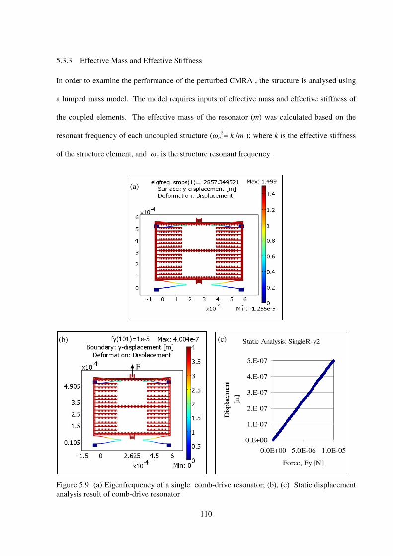
110
5.3.3 Effective Mass and Effective Stiffness
In order to examine the performance of the perturbed CMRA , the structure is analysed using
a lumped mass model. The model requires inputs of effective mass and effective stiffness of
the coupled elements. The effective mass of the resonator (m) was calculated based on the
resonant frequency of each uncoupled structure (ωn2= k /m ); where k is the effective stiffness
of the structure element, and ωn is the structure resonant frequency.
Figure 5.9 (a) Eigenfrequency of a single comb-drive resonator; (b), (c) Static displacement
analysis result of comb-drive resonator
(b)
F
(a)
Static Analysis: SingleR-v2
0.E+00
1.E-07
2.E-07
3.E-07
4.E-07
5.E-07
0.0E+00 5.0E-06 1.0E-05
Force, Fy [N]
Dis
pla
cem
ent
[m
]
(c)

111
The resonant frequency of each uncoupled resonator is determined using an eigenfrequency
analysis (Section 5.3.1). As presented in Chapter 3 (Section 3.3.3.2), the stiffness of the
structure is evaluated in COMSOL Multiphysics using the Static analysis and parametric
solver. By using a static input force, F, the software returns the static displacement of the
structure. The stiffness of the structure is calculated by relating the static input force, F and
static displacement of the structure, δ; (k = F/δ; Equation 3-5). Figure 5.9 shows an example
of the resonant frequency and static analysis result of the single comb-drive resonator from
the FEA. Table 5-6 summarizes the effective stiffness and effective mass of each 5 resonators
of the three CMRA(s).
Table 5-6 Effective mass and stiffness of the CMRA structure elements evaluated using
COMSOL FEA (Note: the three CMRA was coupled with 4 constant coupling spring; kcsp1=
kcsp2= kcsp3= kcsp4= 0.2495 N/m and effective mass, mcsp = 4.116 x 10⁻¹²
kg)
Designed
Parameter
Single
resonator
5 Constant
Mass CMRA
5 Staggered
Mass CMRA
5 Staggered
Stiffness CMRA
Resonator
stiffness [N/m]
19.9796 kR1 = 19.9796
kR2 = 19.9796
kR3 = 19.9796
kR4 = 19.9796
kR5 = 19.9796
kR1 = 19.9954
kR2 = 20.1343
kR3 = 20.1665
kR4 = 20.0868
kR5 = 20.0414
kR1 = 20.3029
kR2 = 20.1807
kR3 = 19.9796
kR4 = 20.0109
kR5 = 20.4824
Resonator mass,
m [nanokg]
3.0615 mR1 = 3.0615
mR2 = 3.0615
mR3 = 3.0615
mR4 = 3.0615
mR5 = 3.0615
mR1 = 3.0941
mR2 = 3.1932
mR3 = 3.2241
mR4 = 3.1616
mR5 = 3.1263
mR1 = 3.0590
mR2 = 3.0596
mR3 = 3.0615
mR4 = 3.0607
mR5 = 3.0575
5.3.4 Change in Comb-Drive Capacitance
The comb drive capacitance is important since it determines the output of current (iout) which
is generated at the readout port of the structure. As discussed in Section 3.5.3.2, in COMSOL
the capacitance was evaluated in the electrostatic application mode using the stationary solver.
Figure 5.10 (a) and (b) show the capacitance analysis result of the single comb resonator. In

112
the analysis, the moving comb was grounded and the voltage input (Vin) was supplied to the
first set of the fixed comb fingers.
Static displacement of comb-drive
resonator vs Input voltage
0.0E+00
5.0E-08
1.0E-07
1.5E-07
2.0E-07
0 5 10 15 20
Input voltage [v]
Dis
pla
cem
ent [m
]
Figure 5.10 (a), (b) Capacitance analysis result of single comb-drive resonator using
COMSOL FEA; (c) A static displacement of the comb-drive resonator
As can be observed (Figure 5.10 (b)) the change of the capacitance (dc/dy) of the resonator is
linear when the overlapping distance is increased from 4 to 6µm. However, above the 6µm
overlapping distance, the change of the capacitance becomes non-linear. From the analysis, at
around 5µm overlapping distance of the fixed and moving fingers (Figure 5.10(b)), the
Capacitance Analysis Result:
SingleR-v2
0.E+00
4.E-14
8.E-14
1.E-13
4 6 8Overlapping distance [um]
Chan
ge
of
Cap
acitan
ce
dc/
dy [
F/u
m]
(a) (b)
Non linear
(c)

113
generated capacitance was 1.2 x 10⁻¹⁴
F/µm. With a 1V potential differences between fixed
and moving fingers, the generated electrostatic force causes 4.66 x 10⁻¹⁰
static structure
movement (Figure 5.10 (c)). By using Equation 3-13 in Chapter 3, the amount of generated
current at a sense voltage (Vs) of 8V is approximately 7.76nanoA. Hence, the current, is more
than sufficient to be processed by the available readout measurement system. Note that a
quick derivation of the output current may be established by estimating the structure
displacement, y (y = (nεobv2)/(kyg), Equation 3-10), and the capacitance between the fixed
and moving comb-drive resonator, C (C = 2nεob (y+yo)/(g)), Equation 3-11). Then, the value
of output current, iout can be estimated from Equation 3-13 by substituting the value of change
of capacitance (dC/dy) and natural frequency of the structure, ω.
5.4 Performance Evaluation of the CMRA-v2: Lumped Mass Analysis
5.4.1 Analysis Overview
In general with N coupled resonators, it is possible to produce (2N – 1) possible output
patterns. With 5 coupled resonators, there are 31 possible sensor combinations. For high
functionality of the sensor structure, the CMRA structure should produce unique response
patterns for all the sensor combinations. This section analyses the performance of the
designed CMRA(s) using a lumped model, when the single resonator sensor absorbs a mass.
As discussed in Section 4.2, the equation of motion for a lightly damped coupled resonators
can be summarized as:-
)()(1111
tFxkxkkkxkxcxmnnnnnnnnnnnn cccc =−+++−+
+−−−ɺɺɺ (Equation 5-1)
Where, m: mass of the resonator, c: damping parameter, k: stiffness of the resonator, kc:
stiffness of the mechanical coupling, F(t): force used to drive the structure and xn is the

114
displacement of the resonator. If we recall Equation 4-8 and Equation 4-9 (Section 4.2), for
the equations of motion of the 5 CMRA (with negligible damping); the equations of motion
are simplified into the form of the matrix eigenvalue problem:
(ω )2
[X] = [M-1
] [K] [X] (Equation 5-2)
Where, ω is the eigenvalue or natural frequency of the system, [X] is a displacement matrix
of the 5 degrees of freedom of the CMRA, [M] is the mass matrix and [K] is the stiffness
matrix of the CMRA.
To solve for the eigenvalue and eigenvectors of the designed CMRA (5 Constant Mass
CMRA, 5 Staggered Mass CMRA, and 5 Staggered Stiffness CMRA), the value of k, kc, and
m (Table 5-6) were substituted in the Equation 5-2. The analysis was repeated to determine
the overall frequency response of the coupled structure, by applying an excitation force F(t)
on the structure array (i.e. at R1, F1(t) = 1 x 10⁻⁶
[N]). From Equation 5-1 and 5-2 the
response of the resonators were computed as follows:-
[X]= [F] [(K – M (ω) 2)]
-1 (Equation 5-3)
Where, [F] is the driving force matrix. The performance of the three CMRA(s) was examined
when a maximum of 1 percent of mass of the single resonator (R) (3.0615 x 10⁻¹¹
kg) was
added to each resonator (R1, R2, R3, R4, and R5) separately.
To examine and confirm the uniqueness of output signals, the stability of system
eigenvectors of the structure and the sensitivity of the mass loading effect on the frequency
response pattern, analyses were repeated by adding a mass of 1 x 10-11
kg, 1 x 10-12
, and 1 x
10-13
kg to the single resonators separately for the three CMRA(s). Note that, to analyse the
effect of the staggered mass on the CMRA sensor performance, the lumped mass analysis was

115
performed only based on the effective mass and stiffness of the 5 resonators and effective
stiffness of the coupling spring (i.e. neglecting the effect of coupling spring mass). By
neglecting the coupling spring mass, the analysed peak to peak modal eigenfrequencies of the
three CMRA(s) will be slightly differed when compared to the FEA result.
5.4.2 Result and Discussion: Frequency Response Pattern of CMRA
Figure 5.11, 5.12, and 5.13 are examples of the frequency response analysis result of the three
CMRA(s), when the first resonator sensor (R1) and the last resonator (R5) absorbs a mass
separately. Note that, all the structures were driven at R1 and the response of the resonators
were monitored at R5. The complete unperturbed and perturbed modal eigenfrequencies of
the structures were presented in Table 5-7, 5-8 and 5-9 respectively.
Figure 5.11 Frequency response analysis result of 5 Constant CMRA; (a) 3.0615 x 10⁻¹¹
kg
mass added at R1 only ; (b) 3.0615 x 10⁻¹¹
kg mass added at R5 only
(b)
1.28 1.29 1.3 1.31 1.32
x 104
0
2.5
5x 10⁻³
Constant CMRA (+3.0615e-11[kg] at R5)
Frequency [Hz]
R
es. A
mp.
[Arb
itra
ry U
nit
]
1.28 1.29 1.3 1.31 1.32
x 104
0
2.5
5x 10⁻³
Constant CMRA
(+3.0615e-11[kg] at R1)
Frequency [Hz]
R
es. A
mp
.
[Arb
itra
ry U
nit
]
(a)

116
Table 5-7 the unperturbed and perturbed modal eigenfrequencies of the 5 Constant Mass
CMRA (note: similar colours indicate that the particular modal frequencies are the same with
respect to the associated mode)
Perturbed
Mass
[kg]
5
modal
frequencies
Initial +
At R1
+
At R2
+
At R3
+
At R4
+
At R5
fM1 12857 12828 12837 12839 12837 12828
fM2 12888 12873 12881 12888 12881 12873
fM3 12968 12955 12965 12942 12965 12955
fM4 13066 13059 13042 13066 13042 13059
3.0615 x
10-11
fM5 13144 13143 13133 13123 13133 13143
fM1 12857 12851 12852 12853 12852 12851
fM2 12888 12881 12885 12888 12885 12881
fM3 12968 12963 12967 12959 12967 12963
fM4 13066 13063 13058 13066 13058 13063
1 x 10-11
fM5 13144 13144 13140 13136 13140 13144
fM1 12857 12857 12857 12857 12857 12857
fM2 12888 12887 12888 12888 12888 12887
fM3 12968 12967 12968 12967 12968 12967
fM4 13066 13065 13065 13066 13065 13065
1 x 10-12
fM5 13144 13144 13144 13144 13144 13144
fM1 12857 12857 12857 12857 12857 12857
fM2 12888 12888 12888 12888 12888 12888
fM3 12968 12968 12968 12968 12968 12968
fM4 13066 13066 13066 13066 13066 13066
1 x 10-13
fM5 13144 13144 13144 13144 13144 13144
Figure 5.11 shows the frequency response patterns for the 5 Constant CMRA using lumped
mass model analyses. Due to the constant mass design, a similar amount of R1 and R5
changes both perturbed conditions generated mirrored frequency response patterns. Table 5-7
clearly indicates, irrespective the amount of mass perturbed in the system, the response of the
first half of the coupled resonators are always similar to the second half of the structure (i.e.
R1//R5 and R2//R4). The results agreed with the finite element analysis result in Section
3.4.5 for the constant mass structure configuration. Hence, if the 5 Constant CMRA is used to

117
detect any single species of mass or material (i.e. in the artificial nose application), only 3
resonators will be useful.
Figure 5.12 Frequency Response Result of 5 Staggered Mass CMRA; (a) 3.0615 x 10⁻¹¹
kg
mass added at R1; (b) 3.0615 x 10⁻¹¹
kg mass added at R5; (c) 1 x 10-13
kg mass added at R1;
(d) 1 x 10-13
kg mass added at R5
Figure 5.12 presents the frequency response pattern of the perturbed Staggered Mass CMRA
and Table 5-8 compares the modal frequencies of the structure when the single resonator
sensor absorbs a mass. From Figure 5.12 it can be seen that 1% of mass (3.0615 x 10⁻¹¹
) or
minimum of 1 x 10-13
kg of mass absorbed by R1 or R5 , produced different A-F curves due
to the staggered mass design of the CMRA. From Table 5-8 modal frequencies, at a
maximum of 3.0615 x 10⁻¹¹
kg or 1 x 10-11
kg mass absorbed by the single resonator, the modal
frequencies of the Staggered Mass CMRA are always distinctive. However, the mass changes
1.26 1.27 1.28 1.29 1.3
x 104
0
2
4
6x 10⁻⁴
Staggered Mass CMRA (+3.0615e-11 [kg] at R1)
Frequency [Hz]
R
esp
.Am
p.
[Arb
itra
ry U
nit
]
1.26 1.27 1.28 1.29 1.3
x 104
0
2
4
6x 10⁻⁴
Staggered Mass CMRA (+3.0615e-11 [kg] at R5)
Frequency [Hz] R
esp
.Am
p.
[Arb
itra
ry U
nit
]
1.26 1.27 1.28 1.29 1.3
x 104
0
1
2x 10⁻³
Staggered Mass CMRA (+1e-13 [kg] at R5)
Frequency [Hz]
Res
p.A
mp
.[A
rbit
rary
Un
it]
1.26 1.27 1.28 1.29 1.3
x 104
0
0.5
1x 10⁻³
Staggered Mass CMRA (+1e-13 [kg] at R1)
Frequency [Hz]
Res
p.A
mp
.[A
rbit
rary
Un
it]
(a) (b)
(c) (d)
fM3: 12794 Hz fM2: 12721 Hz

118
of 1 x 10-12
and 1 x 10-13
kg produces no change in eigenfrequencies. The distinctiveness of
the A-F curve at 1 x 10-13
kg (Figure 5.12(c) and (d)) is only associated to the shift of the
structure response amplitude. If we consider the shift of the modal eigenfrequencies, the
perturbation mass which is less than 1 x 10-12
kg
may be regarded as being below the
detection limit.
Table 5-8 the unperturbed and perturbed modal eigenfrequencies of the 5 Staggered Mass
CMRA
Perturbed
Mass
[kg]
5
modal
frequencies
Initial +
At R1
+
At R2
+
At R3
+
At R4
+
At R5
fM1 12651 12648 12630 12613 12639 12648
fM2 12750 12739 12732 12750 12732 12721
fM3 12809 12794 12802 12794 12809 12794
fM4 12917 12890 12909 12917 12895 12907
3.0615
x 10-11
fM5 12945 12938 12937 12938 12935 12940
fM1 12651 12650 12645 12640 12648 12650
fM2 12750 12747 12744 12750 12744 12742
fM3 12809 12804 12806 12803 12809 12803
fM4 12917 12908 12915 12917 12911 12914
1 x 10-11
fM5 12945 12941 12941 12942 12940 12943
fM1 12651 12651 12650 12650 12651 12651
fM2 12750 12750 12750 12750 12750 12749
fM3 12809 12809 12809 12809 12809 12809
fM4 12917 12917 12917 12917 12917 12917
1 x 10-12
fM5 12945 12944 12944 12944 12944 12944
fM1 12651 12651 12651 12651 12651 12651
fM2 12750 12750 12750 12750 12750 12750
fM3 12809 12809 12809 12809 12809 12809
fM4 12917 12917 12917 12917 12917 12917
1 x 10-13
fM5 12945 12945 12945 12945 12945 12945

119
Figure 5.13 Frequency Response Result of 5 Staggered Stiffness CMRA; (a) 3.0615 x 10⁻¹¹
kg
mass added at R1; (b) 3.0615 x 10⁻¹¹
kg mass added at R5; (c) 1 x 10-13
kg mass added at R1;
(d) 1 x 10-13
kg mass added at R5
As shown in Figure 5.13, the Staggered Stiffness CMRA produces unique frequency response
patterns, when the single resonator sensor (i.e. R1 and R5) absorbs similar amount of mass.
By altering the anchor spring length (Section 5.2), we actually stagger the stiffness and mass
of the Staggered Stiffness CMRA (e.g. comparing R5 and R3 (Table 5-6), at 0.13% mass
change causes 2.52% change in stiffness) . Hence, unique frequency response patterns with
distinctive shift of modal frequencies were observed when a maximum of 3.0615 x 10⁻¹¹
kg
and 1 x 10-11
kg mass absorbed by the single resonator sensor (Table 5-9). Although, 1 x 10-
13kg mass is below the detection limit of the structure (no change in modal eigenfrequencies
(Table 5-9)); but, the structure still sensitive to produce unique change of response
amplitudes due to the different mass and stiffness configuration.
1.285 1.295 1.305 1.315 1.325
x 104
0
0.5
1x 10⁻³
Staggered Stiffness CMRA (+3.0615e-11 [kg] at R1)
Frequency [Hz]
R
esp
.Am
p.
[Arb
itra
ry U
nit
]
1.285 1.295 1.305 1.315 1.325
x 104
0
2
4x 10⁻⁴
Staggered Stiffness CMRA (+3.0615e-11 [kg] at R5)
Frequency [Hz]
Res
p.A
mp
.[A
rbit
rary
Un
it]
1.285 1.295 1.305 1.315 1.325
x 104
0
2
4
6
8x 10⁻³
Staggered Stiffness CMRA
(+1e-13 [kg] at R1)
Frequency [Hz]
Res
p.A
mp
.[A
rbit
rary
Un
it]
1.285 1.295 1.305 1.315 1.325
x 104
0
1
2
3x 10⁻³
Staggered Stiffness CMRA
(+1e-13[kg] at R5)
Frequency [Hz]
Res
p.A
mp
.[A
rbit
rary
Un
it]
(a) (b)
(c) (d)

120
Table 5-9 the unperturbed and perturbed modal eigenfrequencies of the Staggered Stiffness
CMRA
Perturbed
Mass
[kg]
5
modal
frequencies
Initial +
At R1
+
At R2
+
At R3
+
At R4
+
At R5
fM1 12903 12897 12889 12869 12876 12898
fM2 12982 12949 12965 12982 12968 12972
fM3 13053 13038 13053 13033 13047 13035
fM4 13152 13145 13131 13152 13142 13125
3.0615
x 10-11
fM5 13189 13185 13176 13178 13182 13184
fM1 12903 12902 12900 12893 12896 12902
fM2 12982 12972 12976 12982 12977 12979
fM3 13053 13047 13053 13046 13051 13048
fM4 13152 13149 13146 13152 13148 13142
1 x 10-11
fM5 13189 13187 13183 13185 13186 13187
fM1 12903 12903 12903 12902 12902 12903
fM2 12982 12981 12981 12982 12981 12982
fM3 13053 13052 13053 13052 13053 13053
fM4 13152 13152 13151 13152 13151 13151
1 x 10-12
fM5 13189 13189 13189 13189 13189 13189
fM1 12903 12903 12903 12903 12903 12903
fM2 12982 12982 12982 12982 12982 12982
fM3 13053 13053 13053 13053 13053 13053
fM4 13152 13152 13152 13152 13152 13152
1 x 10-13
fM5 13189 13189 13189 13189 13189 13189
5.4.3 Result and Discussion: Stability of System Eigenvectors of CMRA
Figure 5.14, 5.15 and 5.16 display examples of the stability of the system eigenvectors (mode
1) of the three CMRA(s), when a single resonator sensor (e.g. R1 and R5) absorbs different
level of mass (refer to Appendix D and E for a complete eigenvectors stability analysis result
for the two staggered CMRA(s)).

121
Figure 5.14 Stability of eigenvectors analysis result between unperturbed and perturbed
Constant CMRA
Figure 5.15 Stability of eigenvectors analysis result between unperturbed and perturbed
Staggered Mass CMRA
As shown in Figure 5.14, comparing the unperturbed and perturbed eigenvectors of the
Constant Mass CMRA, the system eigenvectors are always unstable even though only a small
amount of mass (i.e. 1 x 10-13
kg) is absorbed by the resonator. Hence, if the unperturbed
1 2 3 4 5-1
-0.5
0
0.5
1
Constant Mass CMRA: Mode 1 Eigenvectors Stability (+1e-11[kg])
Resonator 1 to 5
Eig
env
ecto
rs
Initial
+m@R1
+m@R5
1 2 3 4 5
-1
-0.5
0
0.5
1
Constant Mass CMRA: Mode 1
Eigenvectors Stability (+1e-13[kg])
Resonator 1 to 5
Eig
env
ecto
rs
Initial
+m@R1
+m@R5
(b) (a)
1 2 3 4 5-1
-0.5
0
0.5
1
Staggered Mass CMRA: Mode 1 Eigenvectors Stability (+1e-11[kg])
Resonator 1 to 5
Eig
env
ecto
rs
Initial
+m@R1
+m@R5
1 2 3 4 5-0.8
-0.6
-0.4
-0.2
0
Staggered Mass CMRA: Mode 1
Eigenvectors Stability (+1e-13[kg])
Resonator 1 to 5
Eig
env
ecto
rs
Initial
+m@R1
+m@R5
1 2 3 4 5-1
-0.5
0
0.5
Staggered Mass CMRA: Mode 1
Eigenvectors Stability (+1e-12[kg])
Resonator 1 to 5
Eig
env
ect
ors
Initial
+m@R1
+m@R5
(a) (b)
(c)

122
eigenvectors are used to estimate the mass change pattern of the perturbed structure (using
inverse eigenvalue analysis), a large error is expected to be produced due to the unstable
system eigenvectors of the structure.
Figure 5.15 shows an example of the stability analysis results for the Staggered Mass
CMRA (refer to Appendix D for the complete analysis results). Referring to the Staggered
Mass CMRA design and considering R3 as a reference point, the amount of the staggered
mass between the 5 resonators is: R1 compared R2, R1//R2 (9.91 x 10⁻¹¹
kg) , R2//R3 (3.09 x
10-11
), R4//R3 (6.25 x 10⁻¹¹
), and R5//R4 (3.53 x 10⁻¹¹
kg). Following the eigenvectors
stability against different perturbing masses, the eigenvectors remain stable when the
perturbing mass is significantly smaller than the staggered mass as follows: R1 (at 3.0615 x
10-11
kg perturbation mass), R2 (1 x 10-11
kg), R3 and R4 (1 x 10-12
kg), and R5 (1x 10-13
kg).
The results demonstrate the limit of the amount of perturbation mass that can be perturbed at
each single resonator sensor to ensure stable perturbed eigenvectors.
Figure 5.16 shows the stability analysis results of the Staggered Stiffness CMRA (i.e.
mode 1; refer to Appendix E for the complete analysis results). As different amount of masses
are absorbed by R1 and R5 (i.e. 1 x 10-11
kg, 1 x 10-12
kg or 1 x 10-13
kg) the perturbed
eigenvectors are always stable compared to the unperturbed eigenvectors. When the outer
CMRA resonators were stiffened (i.e. kR1>KR2> KR3 or KR5>KR4>KR3) by reducing the length
of the anchor spring of the resonator, the mass of the resonators was actually reduced. The
configuration of the stiffness of the coupled resonators produced an unsymmetrical staggered
mass with the heaviest mass value in the middle of the coupled structure (R3). Such a
staggered mass configuration provides an effective way to break the structure symmetry for
an effective structure movement. Positioning the stiff resonator at the end of the structure
array slightly restrained the eigenvectors at the end of the array. As discussed in Section 4.6.3

123
such an approach helped to stabilize the structure eigenvectors. Hence the stability of the
Staggered Stiffness CMRA improved significantly at levels of absorbed mass.
Figure 5.16 Stability of eigenvectors analysis result between unperturbed and perturbed
Staggered Stiffness CMRA (single resonator sensor)
5.5 Estimation of Mass Change Patterns of the CMRA Using Inverse
Eigenvalue Analysis
5.5.1 Overview and Analysis
When one of the resonators of the CMRA absorbs mass, we can identify which mass has
changed by using an inverse eigenvalue analysis; this requires a knowledge of the perturbed
eigenvalues (or eigenfrequencies) and perturbed eigenvectors. Since the perturbed
eigenvectors are complicated to measure, the unperturbed eigenvectors will be used in the
estimation of the mass changes pattern of the CMRA. Hence, it is important to ensure that the
1 2 3 4 5-0.7
-0.5
-0.3
-0.1
Staggered Stiffness CMRA: Mode 1
Eigenvectors Stability (+1e-11[kg])
Resonator 1 to 5
Eig
env
ecto
rs
Initial
+m@R1
+m@R5
(a) (b)
1 2 3 4 5-0.7
-0.5
-0.3
-0.1
Staggered Stiffness CMRA: Mode 1
Eigenvectors Stability (+1e-12[kg])
Resonator 1 to 5
Eig
envec
tors
Initial
+m@R1
+m@R5
1 2 3 4 5-0.7
-0.5
-0.3
-0.1
Staggered Stiffness CMRA: Mode 1
Eigenvectors Stability (+1e-13[kg])
Resonator 1 to 5
Eig
env
ecto
rs
Initial
+m@R1
+m@R5
(c)

124
eigenvectors are stable against mass changes. The eigenvectors of the unperturbed system
were used to transform the mass and stiffness matrix into a generalised mass matrix [MG] and
generalized stiffness matrix [KG]. A simple relationship exists between the eigenfrequencies,
ωi and the elements of the generalised mass and stiffness matrices:-
2 ii
ii
G
i
G
K
Mω = (Equation 5-4)
Assuming, a mass ∆m1 is added to resonator 1 (R1), then a perturbed set of eigenvalues will
be obtained; and since the stiffness matrix is unchanged, we may uniquely identify the
generalised mass matrix. We can then transform this back to the real mass matrix, so
identifying ∆m1, if we have the new eigenvectors or if the unperturbed eigenvectors are
sufficiently unchanged. The challenge is to have the CMRA structure design, in which any
small change of masses should give insignificant change to the eigenvectors of the
unperturbed system.
The performance of the three CMRA(s) (5 Constant Mass CMRA, 5 Staggered Mass
CMRA, and 5 Staggered Stiffness CMRA) were examined by adding a mass of 1 x 10-11
kg, 1
x 10-12
kg, and 1 x 10-13
kg separately to each resonator (R1, 2 ,3, 4 and R5). Then the
unperturbed eigenvectors were used to estimate the perturbed mass (epm). Errors of mass
estimation, Eest were calculated by comparing the estimated perturbed mass, epm and the
actual perturbed mass, apm added to the structure:
Eest = | epm - apm| (Equation 5-5)
The performance of the three CMRA(s) was compared by calculating the errors of mass
estimation, Eest for the sensor structures when absorbing similar amount of mass.

125
5.5.2 Result and Discussion
Figure 5.17 Eigenvectors stability analysis; mass change pattern of CMRA estimated using
inverse eigenvalue analysis and error of mass estimation: (a), (d) Constant Mass CMRA; (b),
(e) Staggered Mass CMRA; (c), (f) Staggered Stiffness CMRA
Figure 5.17(a) (b) and (c) compare examples of the estimated mass using the inverse
eigenvalue analysis and the unperturbed eigenvectors of the structure for the 5 Constant Mass
CMRA, 5 Staggered Mass CMRA and for 5 Staggered Stiffness CMRA respectively.
Comparing the error of mass estimation at R1 between the staggered CMRA and constant
1 2 3 4 50
2
4
6
8x 10-13
Staggered mass CMRA: Error of Mass
Estimation (when +m: 1e-12kg at R1)
Resonator 1 to 5
Err
or,
Ees
t [k
g]
1 2 3 4 51
1.5
2
2.5
3x 10
-13
Mass Change Pattern of Staggered mass CMRA (when +m: 1e-12kg at R1)
Resonator 1 to 5
Est
imat
ed M
ass
[kg
]
1 2 3 4 5-5
0
5x 10-11
Mass Change Pattern of Constant Mass
CMRA (when +m: 1e-12kg at R1)
Resonator 1 to 5
Est
imat
ed M
ass
[kg
]
1 2 3 4 52
3
4x 10-11
Constant Mass CMRA: Error of Mass Estimation (when +m: 1e-12kg at R1)
Resonator 1 to 5
Err
or,
Ees
t [k
g]
(a) (d)
(b) (e)
(c) (f)
1 2 3 4 51.5
2
2.5
3x 10
-13
Mass Change Pattern of Staggered
Stiffness CMRA(when+m:1e-12[kg] at R1)
Resonator 1 to 5Est
imat
ed
Mass
[k
g]
1 2 3 4 5
2
4
6
x 10-13
Staggered Stiffness CMRA: Error of
Mass Estimation(when+m:1e-12[kg] at R1)
Resonator 1 to 5
Err
or,
Ees
t [k
g]
(c) (f)
126
CMRA; the error for the Staggered Mass and Staggered Stiffness CMRA (Figure 5.17 (e) and
(f)) was 72% and 71% when the resonator absorbs 1e-12
Kg of mass. However for the
Constant CMRA, (Figure 5.17 (d)), the estimations of mass using the unperturbed
eigenvectors can be considered invalid, since it causes very high error. Further to emphasize,
even though the 70% errors are quite high for the staggered CMRA, we can clearly
distinguish the mass change pattern of the five coupled resonators when only R1 absorbs the
mass.
Therefore, from the analysis presented above it is clear that staggering the mass of
coupled resonators has resulted in the stabilization of the eigenvectors of the structure (refer
to Appendix D and E for the new perturbed eigenvectors compared to unperturbed
eigenvectors for both staggered structure and a complete stability analysis result). As a result,
any small amount of mass absorbed by the resonators, will not affect the designed
eigenvectors of the structure. Hence, it is then valid to use the unperturbed eigenvectors to
estimate any mass changes absorbed by the resonator.
5.6 Impact of Manufacturing Variation on the CMRA performance
5.6.1 Manufacturing Variation Quantification
5.6.1.1 Overview
Monitoring MEMS fabricated geometries is as fundamentally important as tracking material
properties [121]. By measuring the geometrical dimension of the fabricated structure, the
level of the process variation can be estimated. In this research, the geometrical dimension of
the comb-drive resonators which were fabricated using the INTEGRAM SOI micromachining
processes (outsourced) [150] were measured using a scanning electron microscopy (SEM).

127
Using the data, an analysis was performed to estimate the impact of the manufacturing
variation on the performance of the CMRA (Section 5.6.2).
Fundamentally, the key impact parameter is the resonant frequency of the structure:-
Resonant frequency,
m
k=ω (Equation 5-6)
This means that,
∆−
∆=
∆
m
m
k
k
2
1
ω
ω (Equation 5-7)
The variation of the fundamental frequency (∆ω) relates to the change of the structure
stiffness (∆k) and effective mass (∆m) of the structure (Equation 5-7). The change of the
structure stiffness or mass due to the change of the nominal designed dimension causes part to
part variation (e.g. the variation between single resonators) as well as the overall structure.
Figure 5.18 Analysis steps - Impact of manufacturing variation analysis on the CMRA
performance
Figure 5.18 highlights the analysis steps in quantifying the process variation and analyzing the
impact of the manufacturing variation on the CMRA performance. The measured geometrical
dimension of the fabricated structure is analyzed using a statistical analysis. The analyzed
data is used to generate random variables used to represent the geometrical structure
Structure Fabrication
Variation Quantification & Statistical Analysis
Performance of Designed CMRA
Impact of Variation (Lumped Mass Analysis)
Analysis) Frequency Response Measurement: Single and coupled
structure
Random variables generation (to represent structure variation)

128
variations. The generated random variables are then used in the manufacturing variation
analysis in order to estimate the impact of the process variation on the designed CMRA.
5.6.1.2 The variation quantification and Statistical Data Analysis
Figure 5.19 (a) Scanning electron microscope (SEM) images of constant coupled resonators;
(b) Anchor spring; (c) Coupling spring; (d) Comb fingers; (e) Linked mass
To quantify the variation, 3 INTEGRAM chips (5 x 5 mm in size) which contain single and
triple constant mass coupled comb drive resonators were measured using an environmental
scanning electron microscope (XL-30 FEG-ESEM). Refer to Table 5-10 for the nominal
designed dimension of the INTEGRAM resonators.
The geometrical parameters to be measured are based on the number of repeated
elements in the coupled structures (i.e. probability each element will vary due to process
variation) which include length and width of the anchor spring (LASP, bASP), length and width
of the coupling spring (LCSP, bASP), length and width of the linked mass (LLM, bLM), and length
and width of the comb fingers (Lf, bf). It is important to note that since the integrated comb-
drive resonator is a lateral device, the thickness of the device layer has a little effect upon the
(d)
Lf
bf
(a)
(e)
LLM
bLM
(c)
bCSP
LCSP
(b)
LASP(L) LASP(S)

129
resonant frequency of the device and therefore was not measured extensively. Figure 5.19
illustrates the geometrical parameters which were monitored and measured using the SEM.
The geometrical measurements were done using the secondary electron detector in the SEM.
Before the measurement of the structure, the ESEM system was calibrated using 2
magnification standards (19.7 line per mm (low magnification) and 2160 lines per mm (for
high magnification)) [151]. To measure one geometrical dimension of the structure, three
measurements were made and an average is taken to establish 1 data sample of the structure
dimension.
In order to analyze the variation of the geometrical dimension of the fabricated
structure, a simple statistical data analysis was established. The mean (µ) and standard
deviation (σ) of the fabricated structure were calculated using 1-sample t test analysis with 90
percent confidence interval. The variation was calculated in terms of a manufacturing
tolerance, V1 (variation between the fabricated and designed structure) (V1= ((µ – µo)/
µo)*100) and a part to part variation of the fabricated structure (V2 = (σ / µo)*100)). Where,
µ: population mean of the fabricated samples; µo: mean of the nominal designed dimension;
and σ: standard deviation of the sample data analysis.
5.6.1.3 Result and Discussion
Figure 5.20 shows an example of one of the measured geometrical dimension for the comb
finger length with 9.9µm mean (µ) of the population sample. From the data distribution, the
measured dimensions are always less than the nominal design dimension (i.e. 10µm). The
manufacturing tolerance and part to part variation for the length of comb finger for the
selected INTEGRAM chip (Table 5-10) are -0.94% (always less than the nominal design
parameter) and 0.47% respectively.

130
10.0009.9759.9509.9259.9009.8759.8509.825
6
5
4
3
2
1
0
-1
X_
Ho
Length of finger (Lf)_chip5
Fre
quency
Histogram of Length of comb finger_chip5
(with Ho and 90% t-confidence interval for the mean)
Figure 5.20 Example of comb finger length measured data distribution.
Table 5-10 contains the results of the quantified variation data analysis measured on a single
chip. As can be observed, the width of anchor spring (bASP), coupling spring (bCSP), and the
width of finger (bf) with the smallest nominal design dimension (i.e. 3µm sizes) show the
highest manufacturing tolerance and part to part variations. With such level of the part to part
variation, we may presume that the variation may significantly change the stiffness and mass
of resonators; and hence the frequency response of the resonator. To further confirm the
deduction, the quantified variation data were then used in the next section of analysis to
analyze the impact of the process variation on the CMRA sensor performance (5 Constant
Mass CMRA).

131
Table 5-10 Manufacturing Variation data analysis – measured on a single INTEGRAM chip
5.6.2 Impact of Manufacturing Variation Analysis
Due to nature of the manufacturing processes in MEMS, variation is inevitable. However the
variation may help to improve some aspects of the CMRA structure design. As we discussed
earlier in Chapter 3, and 4 the constant Mass design of the CMRA gives a potential problem
in distinguishing any masses absorbed by the sensors since a unique frequency response
pattern is not generated. Furthermore, due to the symmetrical mass design, the perturbed
eigenvectors of the Constant CMRA structure are always different compared to the
unperturbed eigenvectors. In this section an analysis is conducted to identify how the
variation may alter the geometrical dimensions of the 5 Constant Mass CMRA (refer to
Appendix G for the impact of the variation on a single comb-drive resonator) . Each
resonator may have a slightly different mass, which will may help to improve the
Dimension /
(no. of N samples)
Mean -
nominal
Parameter,
µo [µm]
Mean -
fabricated
parameter,
µ [µm]
Standard
deviation
σ
Manufacturing
tolerance
V1[%]
Part to
part
variation
V2 [%]
Anchor Spring
width, bASP / (24)
3
4.298
0.0460
[43.30]
1.53
Anchor Spring
Length, LASP (24)
201 (s)
216 (L)
200.19
214.07
0.6630
0.7250
[-0.40]
[-0.89]
0.33
0.34
Coupling Spring
Width, bCSP / (12)
3 4.295 0.0597 [43.17] 1.99
Coupling Spring
Length, LASP (6)
455
454.37
0.519
[-0.14]
0.11
Width of Linked
Mass, bLM (12)
19 20.09 0.0569 [5.72] 0.30
Length of Linked
Mass, LLM (12)
38 37.67 0.0940 [-0.87] 0.25
Comb finger
Width, bf (24)
3 4.23 0.0506 [41.06] 1.69
Comb finger
Length, Lf (24)
10 9.91 0.0470 [-0.94] 0.47

132
distinguishability of the CMRA output signal. In order to analyze the overall CMRA
performance and the impact of variation, a lumped mass structure model was established
which relates between ωn , k and mR of the 5 coupled resonator array structure (from Equation
5-2).
(ωn )2
[X] = [M-1
] [K] [X]
The numerical analysis was undertaken to calculate the effective mass and stiffness of the
resonators (refer to Appendix F) so that they are comparable with the FEA value. The
numerical derived effective mass and stiffness were then substituted into Equation 5-2. Using
MATLAB the 5 eigenfrequencies and eigenvectors of the CMRA were computed. The
manufacturing variation was introduced into the model using random variables which were
generated based on the quantified µ (mean) and σ (standard deviation) of the fabricated
structure which was described earlier in Section 5.6.1.
As an example, a random variable for finger width RanWFin :
RanWFin = LoLWFin + (UpLWFin - LoLWFin) * Rand (1,N) (Equation 5-8)
Where, LoLWFin, is the lower limit of the WFin variable;
= µWFin – (TWFin (N) * σ WFin)/sqrt (N + 1) (Equation 5-9)
UpLWFin is the upper limit of the WFin variable;
= µWFin + (TWFin (N) * σ WFin)/sqrt (N + 1) (Equation 5-10)
Rand (1,N) is a MATLAB command to generate N random numbers between 0 and 1 (i.e.
based on a uniform distribution). TWFin (N) is a statistic 1 sample t test value for the N sample
size of the quantified parameters. The generated random variables were then fed into the
lumped mass model analysis to represent all the considered geometrical changes due to the

133
manufacturing variations. The effect of variation (i.e. based on worst case scenario; change of
length and width of the anchor spring, comb fingers and linked mass)2 before and after mass
were added to the structure were simulated.
5.6.2.1 Result and discussion
Figure 5.21 The effect of manufacturing variation on the Constant Mass CMRA; (a), (b)
Measurability of sensor output signal; (c) Distinctiveness of 5 modal frequencies when single
resonator R1 and R5 absorbs similar amount of mass; (d) The eigenvectors of initial and
single resonator mass change
2 A sensitivity analysis such as using the Monte Carlo simulation to indicate which are the most important
geometrical parameter in influencing the performance of the CMRA is beyond the scope of the thesis. However,
since the CMRA is a lateral device, from the analytical expression for the effective stiffness and mass of the
integrated comb-drive resonator (Appendix F, Equation F-1 and F-3), the resonator stiffness (k) is inversely
proportional to length cubed (L) and proportional to width cubed (b) of the resonator anchor spring. The
sensitivity of change of mass (m) with the change of b and L is less compared to the change in stiffness. The
structure thickness (h) has a small effect on the resonator natural frequency (a proportional effect of h on the
stiffness and resonator mass is cancelled to each other); So, the stiffness dominates the structure resonant
frequency, which is related to the width and length cube of the resonator anchor spring.
1 2 3 4 5-1
-0.5
0
0.5
1
Stability of Eigenvector Analysis (with Variation-Mode 4 )
Resonator 1 to 5
E
igen
vec
tors
Initial
+m @R1
+m @R2
+m @R3
+m @R4
+m @R5
0 50 1000
0.025
0.05
0.075
0.1
Eigenmodes Analysis
(with Variation)
Eig
env
ecto
rs
Total Variations
(a)
0 100 200 300 400 500-10
-5
0
5
10
Eigenfrequency Analysis
Constant CMRA with Variation
Fre
qu
ency
Dif
fere
nce
s
fm (
R1
vs
R5
) [H
z]
Total Variations
1 2 3 4 5-0.8
-0.4
0
0.4
0.8
Eigenmodes of Constant CMRA
(Initial Condition, with Variation)
Resonator 1 to 5
Eig
envec
tors
mode1
mode2
mode3
mode4
mode5
(a) (b)
(c) (d)

134
Fig. 5.21 shows analysis results of the effect of manufacturing variation on the CMRA sensor
performance. The change of the geometrical dimensions due to the process variation, may
alter the mass and stiffness of the coupled elements. Considerable increase in some resonator
stiffness or mass will reduce some eigenvectors of the structure. As a result some modes of
the CMRA frequency response will approach zero; instead of getting 5 response peaks for the
5 CMRA, only 4 peaks or less may be observed when the frequency response of the structure
is measured. Figure 5.21(a) displays the effect of variation analysis result on the relative
displacement of the coupled resonators on a particular simulation run. Assuming that
eigenvectors which less than 0.025 is unable to be measured; out of 100 CMRA variations
only 68% may produce 5 response peaks. Figure 5.21(b) shows an example of eigenmode
analysis of the unperturbed CMRA; due to the variation, the eigenvectors of mode 1 (i.e. R1)
retracted to zero. As a result, if the frequency response of the predicted CMRA is measured at
R1, only 4 modal frequencies are expected to be measurable.
However, as a result of the alteration of the mass and stiffness of the coupled elements,
some modal frequencies of the structure may be changed, which will enhance the uniqueness
of the frequency response of the Constant Mass CMRA. Figure 5.21 (c) demonstrates the plot
of eigenfrequency differences of the 5 CMRA when R1 (resonator 1) and R5 absorbs similar
amount of mass separately. Instead of having 5 similar modal frequencies due to the constant
mass design of the coupled resonators, it can be predicted that the variation may significantly
modify the distinctiveness of the frequency response of R1 and R5 single resonator mass
change. If we consider a 5Hz frequency difference or below is less distinguishable response;
from the impact analysis, 86.6% out of 100 CMRA produces distinctive response pattern (i.e.
frequency difference is more than 5 Hz). Figure 5.21(d) shows an example of stable
eigenvectors of a single resonator mass change when the variations were imparted in the

135
analysis. It can be predicted that due to the change of some mass of the coupled resonators,
the stability of eigenmodes of some single or multiple resonators sensor may be improved.
5.7 Summary and Conclusion
This chapter presents and discusses the second version of the CMRA design based on the
integrated coupled comb-drive resonators. The 5 Constant CMRA was designed in order to
examine the effect of the manufacturing variation on the performance of the constant mass
CMRA. For uniqueness of the frequency response pattern and stability of the system
eigenvectors, the research proposed two staggered CMRA structure designs; (i) 5 Staggered
Mass CMRA, and (ii) 5 Staggered Stiffness CMRA.
Driving or monitoring the CMRA structure at different resonators may produce
different response patterns, depending on the mass and stiffness configuration of the
resonator. For the specific CMRA design, the difference of the response pattern is related to
the response amplitude of the structure. The 5 modal frequencies of the structure remain
similar with respect to any drive or readout. For example, driving the ideal Constant CMRA
from resonator 1 (R1) and measuring the output either at R1 or R5 produce similar response
pattern due to the symmetrical structure mass design. However, driving or measuring the
staggered CMRA at different resonators will cause different frequency response pattern for
the structure. The differences are associated with the unique response amplitude of the
resonators due to different mass and stiffness configurations of the resonator.
Although with the CMRA-v2 structure design, flexibility arises in measuring the output
signal of the structure (i.e. different drive and readout selections); the drive or readout points
need to be selected properly in order to measure all the 5 response peaks of the structure. As
analysed for the Constant CMRA, due to the symmetrical design, measuring or driving the

136
structure at R3 produces only 3 peaks of responses. There are 2 missing eigenfrequencies
associated to the eigenmode 2 and 4. Referring to the R3 at the two missing modes, the
resonator reacts as a node (0 eigenvector) with zero resonator displacement.
From the FEA analysis result of the unperturbed CMRA, it is confirmed that the second
version of the CMRA is measurable with sufficient capacitances to be processed by the
readout measurement system. The uniqueness of the frequency response pattern and the
stability of the system eigenvectors after mass is added to the resonators (perturbed structure)
were then analysed in Section 5.4 using the lumped mass model analysis.
From the lumped mass analysis of the three CMRA(s), it was confirmed that the
Constant Mass CMRA always produces similar frequency response pattern for the first and
second half of the resonator array. The response of R1 mirrors R5 and R2 mirrors R4.
Furthermore the system eigenvectors of the structure is always unstable. The structure was
then further analysed in Section 5.6, to examine how the manufacturing process variation may
affect the performance of the Constant Mass CMRA.
For the staggered CMRA design, both structures always produce unique frequency
response patterns for any single resonator mass changes. Considering the uniqueness of the
CMRA modal frequency shift, the perturbing mass which is less than 1 x 10-12
kg
may be
regarded as being below the detection limit. From the eigenvectors stability analysis, the
eigenvectors of the Staggered Mass CMRA remain stable when the perturbing mass is
significantly less than the staggered mass. At a minimum and maximum staggered mass of
3.09 x 10⁻¹¹
kg (R3 compared R2) and 9.91 x 10⁻¹¹
kg (R2 compared R1), the limit of the
perturbing mass for a single resonator mass change is as follows: 3.0615 x 10⁻¹¹
kg (R1), 1 x
10-11
kg (R2), 1x 10-12
kg (R3 and R4), and 1x 10-13
kg (R5). By staggering the length of
resonator anchor spring for the Staggered Stiffness CMRA (i.e. at minimum and maximum

137
staggered mass of 6 x 10-13
kg (R2//R1) and 3.2 x 10⁻¹²
kg (R5// R4)), all the eigenvectors of
the single resonator mass change remained stable even though the perturbing mass is slightly
higher than the staggered mass (i.e. 1 x 10-11
kg). Restraining the resonator displacement at
the end of the structure array improves the eigenvectors stability.
To confirm the stability of the system eigenvectors of the three CMRA(s) structure, the
inverse eigenvalue analysis was performed to estimate the amount of perturbed mass using
unperturbed system eigenvectors in Section 5.5. For the Constant Mass CMRA, the
eigenvectors of the perturbed structure are always unstable compared to unperturbed
structure; the inverse eigenvalue analysis produced no valid mass change pattern. The
determination of mass changes pattern of both staggered CMRA(s) produced an error about
70%. Although the error between the actual perturbed mass and estimated perturbed mass are
considered high, but the mass change pattern of the structure was clearly observed.
Manufacturing variation in MEMS fabricated device causes the structure tolerance and
part to part variation. From the variation quantification of the INTEGRAM chip, the variation
is more significant for smaller nominal geometrical dimensions than larger structures. An
example for the 3µm nominal dimension of the anchor spring width, the manufacturing
tolerance is about 43%, and part to part variation is estimated around 1.53 percent. From the
impact of the manufacturing variation analysis on the Constant Mass CMRA performance, the
variation may reduce the measurability of the frequency response output of some of the
coupled sensors. However, it can be predicted that the variation may help to naturally stagger
the geometrical dimension of the CMRA for uniqueness of the response patterns of the
CMRA as the mass detection sensors for the artificial nose. The variation may help to modify
the stability of the CMRA system’s eigenvectors, so that it will be insensitive to any small
amount of mass absorbed by the sensor.

138
To summarize, in order to confirm the performance of the CMRA sensor (i.e. measurability
and uniqueness of the frequency response of the 5 eigenmodes, stability of the structure
eigenvectors for estimation of the mass change pattern of the coupled sensors, and the effect
of manufacturing variation on the CMRA frequency response), the three CMRA(s) structures
(5 Constant Mass, 5 Staggered Mass, and 5 Staggered Stiffness) will be in-house fabricated
(Chapter 6). The single comb-drive resonator also will be fabricated in order to examine effect
of the input driving voltage, vacuum chamber pressure and mass loading effect on the
resonator frequency response. Three similar single resonators of fixed-fixed beams and
integrated comb-drive resonators are fabricated on a single chip in order to observe how the
process variation may affect the frequency response of the single resonator.

139
CHAPTER 6 - FABRICATION AND PACKAGING
6.1 Introduction
This chapter describes the fabrication processes of the CMRA, which includes:-
• Single resonator: fixed-fixed beam (CMRA-v1) and comb-drive resonator
• 5 Constant Mass, 5 Staggered Mass and 5 Staggered Stiffness CMRA (CMRA-v2)
The single fixed-fixed beam resonator was fabricated using 5µm SOI (silicon-on- insulator)
wafer and the CMRA-v2 was fabricated using 20µm SOI wafer. Section 6.2 begins with the
SOI material selection. The fabrication processes are described in Section 6.3. Section 6.4
describes the Mask Design in order to realize the CMRA structure. Processes details to
fabricate the CMRA are discussed in Section 6.5. The fabricated structure is observed at each
major process stage using an Optical Microscope (OM) or SEM (Scanning Electron
Microscope). Section 6.6 discusses the observed structure and highlights the constraints in
the process fabrication. In order to measure the output signal of the CMRA, the structures are
metalized and wire bonded. Both processes are discussed in Section 6.7. To examine the
effect of mass loading on the frequency response pattern of the CMRA, a platinum (Pt) mass
using a focused ion beam machine (FIB) is deposited on the single and the coupled resonators
(CMRA-v2). The experiments and processes related to the FIB machine is highlighted in
Section 6.8.
6.2 Single-Crystal Silicon and Silicon-on-Insulator (SOI) Materials
Silicon-on-insulator (SOI) material is a silicon (Si) wafer having an oxide layer buried below
the surface of a thin film of single-crystal silicon layer. The SOI is of interest for MEMS
because it provides a relatively simple way to fabricate suspended structures in the single-

140
crystal silicon [131]. The wafer offers great advantages for the resonator technology, where it
employs a single sided wafer processing approach with etch selectivity. The suspended
structure can be released by removing the buried oxide layer between the silicon device layer
and the silicon handle layer. The oxide can be removed either using wet etching or dry
etching processes [152].
Table 6-1 SOI wafers thickness for CMRA structure fabrication
SOI wafer layers Thickness of layer, µm
(SingleR-Fixed-fixed beam)
Thickness of layer, µm
(Single and CMRA-v2)
Silicon device layer 5 20
Buried oxide layer (BOX) 2 2
Silicon handle layer 450 500
The SOI wafer material (Table 6-1) was chose for the CMRA structure fabrication due to
excellent properties of the silicon crystal for the resonator and the available processes to
fabricate the structure. The single-crystal silicon has excellent resonating properties such as
very high intrinsic Q-factors, it surpasses an aluminium in strength to-weight ratio, does not
show mechanical hysteresis or fatigue and has a low thermal expansion coefficient [131]. It
therefore, makes an ideal material for the resonators and high performance sensors such as the
CMRA.
The MEMS silicon resonator also can be designed to be integrated with electronic
circuits, sensors [95] or IC (Integrated Circuit) technology [153]. The silicon and SOI
material provides technological advantages for the CMRA fabrication since multiple
resonators can be designed, and released on a single chip. Using the SOI material technology,
many devices can be realized and fabricated on a single wafer.

141
6.3 Overview of the Fabrication Process Flow and Structure Packaging
Figure 6.1 Process Flow of CMRA Fabrication (Note: blue arrow is only for 20µm SOI
device layer structure (CMRA-v2))
MEMS processes can be divided into bulk micromachining and surface micromachining [17].
Bulk micromachining processes were used to fabricate the CMRA structures. In bulk
micromachining processes, material is selectively removed from a substrate by chemical
etching [131]. Figure 6.1 summaries the fabrication process. The principal steps are resist
coating, pattern transfer using lithography, development process, DRIE (dry reactive Ion
etching), and HF released process.
Wafer Cleaning, Resist Coating & soft bake
Dry Reactive Ion Etching (Photoresist Mask)
Structure Releasing (HF)
Metallization
Fixed-fixed beam resonator: In-house (Gold)
CMRA-v2: Out-sourced (Aluminium)
Structure Observation
Structure Observation
Lithography & Resist Development
Wafer Cutting, Photoresist Stripping & Cleaning
Structure Observation
Structure Movement Observation)
Wire Bonding
Continuity/ short circuit checking
Dry Reactive Ion Etching (Silicon Oxide mask)
Structure Observation
5 µm SOI
device layer
Mask design &
Fabrication (Out Source)

142
Figure 6.2 is a schematic diagram of the cross section of both the 5µm and 20µm Si devices at
each stage of the fabrication process.
(a)
Resist coating
(f)
Resist coating
(b)
Photolithography and development
(g)
Photolithography and development
(c)
RIE
(h)
RIE: SiO2 and Si
(d)
Stripping off resist and wafer
cleaning
(i)
Stripping off resist wafer cleaning
(j)
Further RIE
(e)
HF release
(k)
HF release
Resist; Si Oxide Si device; Buried oxide (BOX) ; Si handle
Figure 6.2 schematic diagram of structure device layers at each of process step; (a) – (e): 5µm
Si structures; (f) – (k): 20µm Si structures
When fabricating the 5µm Si devices SOI, the photo resist layer was used to etch the 5µm
silicon device layer directly (Figure 6.2(a) – (c)). In contrast, the 20µm Si devices employed 2
mask layers (photo resist and SiO2 mask layer); the photo resist layer was used to etch the
SiO2 mask layer and about one third of the Si device layer (Figure 6.2(f) - (h)). The structures
were then finally etched using the oxide mask layer (Figure 6.2(j)) after wafer dicing process
and stripping off the resist.

143
Often, photo resist is not tough enough to withstand a longer etching process (i.e. to deep etch
20µm Si devices). In such case, a thin film of a tougher material is deposited and patterned
using a photolithography [154] . In the fabrication of the CMRA-v2, the SOI wafer with a
160nm silicon oxide thin film was deposited on the top layer of the wafer (out-sourced). The
oxide film acts as the main etch mask during the etching of the Si material and as the
secondary layer to cover the structure during wafer cutting process. The CMRA based on the
comb-drive resonator structure is a complex structure with many sub-structure elements. For
the 5 coupled resonators, the structure contains 5260 fingers, 20 anchor springs and 4
coupling springs. With such a structure the chances that some of the structural elements may
be broken or contaminated during wafer cutting are high. The SiO2 mask layer is very
important in order to cover the structure during wafer dicing process.
Processes details for both 2 different Si devices thicknesses are provided in Section 6.5.
6.4 Mask Design
The mask is crucially important in bulk micromachining processes to transfer the pattern of
the structure onto the wafer using a lithography process. The mask not only includes a design
and layout of the structures on a single chip, but also arrangements of different chip designs
on a wafer. To explain the mask design, this section discusses the mask design for the second
version of the CMRA (CMRA-v2). The mask comprises of 4 designs of the CMRA-v2; (1) 5
Constant Mass CMRA, (2) 5 Staggered Mass CMRA, (3) 5 Staggered Stiffness CMRA and
(4) Single comb drive resonator. The structures were laid out on 3 separate chips (5 x 5 mm).
The mask was designed to ensure the structure will be successfully etched and released; the
wafer can be diced to an appropriate chip packaged, wire bonded and electronically tested.

144
6.4.1 Type of mask
Figure 6.3 (a) SEM image of comb finger, fabricated using polyester film mask; (b) A photo
of the chrome glass mask for the CMRA-v2 structure fabrication
The mask material determines the final quality of edge of the fabricated structure. Figure 6.3
(a) is an example of wavy edge comb fingers which were patterned transfer using a polyester
film mask. To improve the edge of the structure, glass chrome mask (Figure 6.3 (b)) was
used to lithographically transfer the structure pattern.
6.4.2 Etching Channel Aspect Ratio
Figure 6.4 Top view of a portion of the resonator design with a minimum channel width of
3µm (Note: all dimensions in µm)
Comb finger
Etch area
(White color)
5
5
15
Gap = 3
5
Anchor pad 16
5

145
The aspect ratio refers to the ratio between the depth and the width of a channel to be etched
using a reactive ion etching process (RIE). As shown in Figure 6.4, the channel to be etched is
the area where the resist has been removed after a lithography and development process
(positive photo resist). Increase in the aspect ratio, slows the etching process [150]. With
20µm CMRA structure thickness, the channel etching process is controlled by fixing the
minimum width of the channel to be etched to 5µm. Hence, the maximum aspect ratio was
kept to 4:1. However, the higher aspect ratio (6.7:1) for the gap between the fixed and
moving fingers which was designed with 3µm is unavoidable (Figure 6.4). Therefore, more
care is required during the structure fabrications to ensure the gap area is properly etched.
Furthermore, to ensure the structure is etched uniformly, it is important for all the channels to
be designed with even aspect ratios.
6.4.3 Size of the Suspended and Anchored Structure
The CMRA mask was designed to ensure that the suspended structure is successfully released
using an HF (hydrofluoric acid) etching process. The important considerations are the
maximum size of the suspended structure to be released and also the minimum size of bonded
pads to be retained to anchor the fixed structure. To ensure the CMRA is released evenly, all
the structures were designed with a maximum of 5µm width. To design the anchor pad size,
a guide provided by the INTEGRAM (Europractice) [150] was used. For a maximum of
50µm structure to be released a lateral undercut is in excess of 35µm. Hence, to release the
maximum of 5µm beam, the lateral undercut is at least 3.5µm per edge. To securely retain the
pad after HF release, the pad was designed at least four times the size of undercut (14 x
14µm).

146
6.4.4 Size of Wire Bonded Pad
Figure 6.5 Schematic of wire bonded pads of the comb drive resonator
To ensure successful wire bonding process the wire bonded pads need to be designed at least
100 x 100µm sizes. Due to space constraints, the CMRA-v2 wire bonded pads were designed
slightly small in terms of the pad width (95µm) but the pad length was increased to 237µm
(Figure 6.5).
6.4.5 Gap and Alignment for Chip Dicing Requirement
To ensure the wafer can be diced properly into chips a cutting mark (Figure 6.6) on the wafer
is necessary to align the cutting lines during the dicing process. Since, 3 different chips
designs were placed and repeated on the mask, a chip identification mark was included
(Figure 6.6).
95 µm
237 µm
Wire bonded pad
Wire bonded pad
Wire bonded pad
Wire bonded pad

147
Figure 6.6 A portion of schematic of mask design with cutting mark and cutting width
6.5 Detail Fabrication Processes
6.5.1 Soft Wafer Cleaning
The process is started by cleaning the SOI wafer. While the wafer is placed on the spinner,
acetone was sprayed on the wafer surface, and the spinning process started. Before the
acetone is dry, the IPA (Isopropyl Alcohol) is sprayed onto the wafer and the speed of the
spinner is increased. To dry the wafer, the soft cleaned wafer was pre baked on a hot plate at
least for 50 seconds and at 115oC.
6.5.2 Primer and Resist Coating
The research used HMDS (Hexamethyldisilizare) as a primer coating and S1805 a positive
photo resist. The HMDS was employed to help an adhesion of the photo resist with the wafer.
To ensure clean resist coating, the primer and the resist were applied on the wafer using a
syringe and a PVDF filter media (Figure 6.7). Approximately 2 to 3ml HMDS liquid was
dropped slowly at the centre of the wafer and the wafer was spun using 3 stages of spinner
Chip mark:
Staggered Mass
CMRA
60µm
Cutting mark

148
speed (480rpm, 10s; 3000rpm, 45s; and 480rpm, 10s). Immediately, after that around 3 to
5ml S1805 was applied and spun on the wafer at 3 stages of spinner speed (200rpm, 10s;
3000rpm, 30s; and 480rpm, 10s). Figure 6.2(a) and (f) show the schematic of the resist layer
(red colour) for both 5 and 20µm SOI wafers respectively.
Figure 6.7 (a) PVDF filter media used to filter the resist; (b) The filter fixed to the syringe tip
Before patterning, the wafer was soft baked at a temperature of 115oC on the hot plate for 2 or
3 minutes. It is important to note that the flatness of the spinner and the smoothness of hot
plate have significant effects on the evenness of the resist coating across the whole wafer.
The soft bake time may have significant effects on the exposure time (lithography) and
development process which is further explained in the next section.
6.5.3 Pattern Transfer Using Lithography and Development Process
Using the chrome mask, the SOI wafer which was coated with photo resist is patterned
transfer using a Canon Mask Aligner (PLA-501 FN, Figure 6.8). As emphasized by Fedder
[155], to ensure an accurate pattern transfer, the exposure and process parameters which need
to be considered are wavelength (λ) of the radiation source, resist thickness, exposure time,
surface roughness of the structure and temperature of the exposure operation. The wafer was
exposed under UV (ultraviolet) light using a hard contact scheme. This is the most crucial
(a) (b)

149
stage to ensure the structure pattern is correctly transferred, with the intended geometrical
shape, remains clean, and is free from any defects. The exposed photo resist was then
developed using MF 319 to create the desired etch mask for the subsequent dry etching
process.
Figure 6.8 Mask aligner machine (PLA-501 FN) for photolithography process
Table 6-2 Experiment data: the effect of different soft bake time, exposure time and
development time on comb finger pattern (CMRA-v2)
Experiment Soft bake time
(minutes)
Exposure time
(seconds)
Development time
(seconds)
3 3.8 30 Effect of soft
bake time 5 3.8 30
2 2 60 Effect of
exposure time 2 4 60
3 3.6 10 Effect of
development time 3 3.6 20
To examine the effect of soft bake time, exposure time and development time, the resist was
spun on several plain Si wafers. The effect of the time was examined by soft baking a wafer
for 3 and 5 minutes separately and other exposure and development time were fixed (refer to
Table 6-2). Then the developed wafer was observed (across the whole wafer based on 3

150
points observation) using an optical microscope. Particular attention was given to the pattern
of the comb fingers. Refer to Section 6.6.1 for the result of observed structures.
CNS and Xie [156] proposed that the S1805 may be soft baked at 3 minutes, exposed
between 4 to 5 seconds and developed at 1 minute. After several trial processes, the 5µm
device and 20µm device thickness were exposed and developed for 4s, 60s and 3.6s, 20s
respectively.
6.5.4 Reactive Ion Etching (RIE) Process
In RIE process, a glow discharge creates chemically reactive ions and radicals of etch gases.
The reactive radicals adsorb on the silicon and react to form volatile products. The process
also is assisted by ion bombardment which gives the etch process a certain directionality [131,
157]. To etch the silicon a mixture of Sulphur Hexafluoride gas (SF6), Oxygen (O2) and
Octafluorocyclobutane (C4F8) was used. Overall, the gas combinations, pressure and plasma
power influence the etch profile of the structure.
Figure 6.9 Surface Technology System (STS machine)
The wafer area which is not protected with the photo resist was dry etched using the surface
technology system (STS machine, Figure 6.9). As an example, for the 5µm SOI device the
wafer was etched for 2minutes and 40seconds. For 20µm SOI device, at the first etching

151
stage, the 160 nm oxide mask layer was etched at 6nm per minute and further etching was
continued to etch around 1/3 of the Si device layer. In the second stage (after wafer cutting
and stripping off resist), the diced and cleaned chips were stuck on a plain silicon wafer using
3195M Thermal Release tape and the remaining 2/3 of the Si layer was etched.
Before a structure release, it is important to ensure that the structure is etched to the
buried oxide layer (BOX). This can be confirmed by observing the colour of the etched layer
under the optical microscope. The colour may look greenish or light purple depending on the
thickness of the Si device and the BOX layer. Due to some tolerance of the Si device layer
thickness, multiple mixed colours such as yellow, green, grey and white can be observed
across the wafer surface before the etched layer approaches the BOX. The BOX layer is
confirmed once all the colours disappear.
6.5.5 Wafer Cutting Process
Figure 6.10 (a) DAD 320 (wafer dicing saw machine); (b) Diamond blade; (c) Wafer stuck on
the tape holder and clamped on the vacuum chuck during cutting process; (d) Cut wafer
(a)
(c)
Wafer stuck
on the tape Tape holder
Vacuum
chuck
(b) (d)

152
In order to release the suspended structure, the wafer was diced and further processes were
carried. To dice the wafer, the research used the wafer dicing saw machine (DAD320, Figure
6.10(a)) and NBC-Z 1060 diamond blade (Figure 6.10(b)) with a size of 56.8 (outer diameter)
x 0.05 (thickness) x 40mm (internal Diameter)). Figure 6.10(c) shows the wafer which was
stuck on a tape holder and clamped on the vacuum chuck during the cutting process and (d)
the wafer after dicing process respectively.
6.5.6 Chip Cleaning and Stripping off Resist
To remove dust and contamination from the cutting process and also to strip off the photo
resist mask layer, the selected chips from the diced wafer were cleaned using acetone, and
IPA. After cleaning with IPA, the chip was rinsed using the ionised water and blown with
nitrogen gun. The cleaning process in acetone and IPA may take few minutes or longer
depending on the soft bake time of the wafer after resist coating process. In general, longer
soft bake time, harden the resist and hence make it more difficult to remove the resist. If the
problem persists, it is necessary to clean the chips using O2 plasma (STS machine). The
cleaning time using O2 may vary from 3 to 10 minutes depending on the lithography
patterning process parameters.
6.5.7 HF Release Process
HF wet etching may be used to release the CMRA structure from the SOI material. The
process can be done by dipping the chip which was held with Teflon tweezers, in HF
(hydrofluoric) acid at 40% concentration. The HF liquid etches the buried oxide underneath
the suspended structure at about 1µm per minute. The etching process was terminated by

153
dipping and rinsing the chip with deionised water. The chip may be dried using CO2 (Carbon
dioxide) critical point drying or using Cyclohexane freeze drying process. Or using other
simple ways, the chip was rinsing in deionised water several times after HF wet etching
process; then, the water was replaced with isopropanol (IPA) at least twice. Finally, the chip
(still held with tweezers) was placed in a clean bottle slowly dried overnight. In most drying
processes the released structure tends to stick to the substrate [131]. For the CMRA-v2
structure the problem is more severe, with stictions occurring between the fixed and moving
comb fingers. Refer to Section 6.6.4 for examples of observed structure after HF liquid.
Figure 6.11 HF vapour release kit setup
To solve the problem the research employed HF vapour processing. An HF vapour release kit
was developed (developed by Anthony, Figure 6.11). The chip was attached to the bottom
surface of the head (chip holder, Figure 6.11(b), (c)) of the teflon bottle and the surface was
heated between 32 to 35oC using the connected thermocouple. Once the actual working
temperature was achieved, the chip holder was transferred to the bottle which contains HF
HF Liquid
Chip attached
to the Teflon
surface
Bottom view of the
head of bottle
Place to fix the
chip to be
released
(a) (b)
(c)
Chip holder
Connection (to set and
check the temperature level)
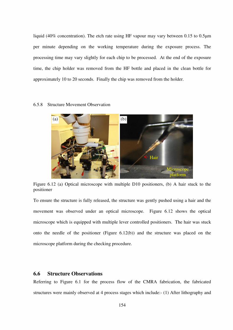
154
liquid (40% concentration). The etch rate using HF vapour may vary between 0.15 to 0.5µm
per minute depending on the working temperature during the exposure process. The
processing time may vary slightly for each chip to be processed. At the end of the exposure
time, the chip holder was removed from the HF bottle and placed in the clean bottle for
approximately 10 to 20 seconds. Finally the chip was removed from the holder.
6.5.8 Structure Movement Observation
Figure 6.12 (a) Optical microscope with multiple D10 positioners, (b) A hair stuck to the
positioner
To ensure the structure is fully released, the structure was gently pushed using a hair and the
movement was observed under an optical microscope. Figure 6.12 shows the optical
microscope which is equipped with multiple lever controlled positioners. The hair was stuck
onto the needle of the positioner (Figure 6.12(b)) and the structure was placed on the
microscope platform during the checking procedure.
6.6 Structure Observations
Referring to Figure 6.1 for the process flow of the CMRA fabrication, the fabricated
structures were mainly observed at 4 process stages which include:- (1) After lithography and
Hair
Microscope
platform
(a) (b)

155
development process; (2) Reactive Ion etching (RIE); (3) Stripping off resist (before HF
process); and (4) After HF release process. The structure was observed using an optical
microscope (Ergolux 200, Figure 6.13(a)) and dual beam FIB/SEM system (EDAX DB235,
Figure 6.13(b)).
Figure 6.13 (a) Optical Microscope (Ergolux 200); (b) Dual beam FIB/SEM system (EDAX
DB235)
6.6.1 Observation 1: Photolithography and Development Process
Figure 6.14 The effect of soft bake time (OM image, 3 observation points; micrographs scales
at 100x magnification); (a)-(c): 3 minutes soft bake time, 3.8 s exposure, and 30 s
development; (d)-(f): 5 minutes soft bake time, 3.8 s exposure, and 30 s development
Figure 6.14 shows the OM image of the comb fingers which were soft baked at 3 minutes
((a)-(c)) and five minutes ((d)-(f)) respectively. 3 minutes soft baking time may be sufficient
2
3
1
(a) (b) (c)
(d) (e) (f)
(b) (a)

156
to process the CMRA-v2, where the size of the gap between fingers almost similar with the
size of the finger (was designed with 3µm gap and 3µm finger width, refer to Chapter 5).
Compared to the structure which was baked for 5 minutes, the gap appears to be much
smaller. Longer baked time increases the hardness of the resist; hence the resist is more
difficult to develop. As can be observed, some finger tips are slightly bigger than the finger
base (e.g. (f)). This is expected due to the large exposed area at the finger base, where the UV
light is accumulated in the area compared to the finger tip area.
Figure 6.15 The effect of exposure time (micrographs scales at 100x magnification); (a)-(c): 2
minutes soft bake time, 2 s exposure, and 60 s development; (d)-(f): 2 minutes soft bake time,
4 s exposure, and 60 s development
Figure 6.15 illustrates the effect of different exposure times on the structures which were
processed on two separate wafers. At similar soft bake time and development time,
increasing the exposure time from 2s ((a)-(c)) to 4s ((d)-(f)), definitely decreased the size of
the comb finger since the gap between fingers is increased. Increasing the exposure time,
increases the softened resist area. Hence, enlarged the gap areas and reduced the size of
fingers.
Figure 6.16 shows the result of the structures which were soft baked at 3minutes, exposed at
3.6s and developed at 10s ((a)-(c)) and 20s ((d)-(f)) separately. As can be seen 10s
2
3
1
(a) (b) (c)
(d) (e) (f)

157
development time is not sufficient to clean the exposed resist. The structures only properly
developed at 20s.
Figure 6.16 The effect of development time (micrographs scales at 100x magnification); (a)-
(c): 3 minutes soft bake time, 3.6 s exposure, and 10 s development; (d)-(f): 3 minutes soft
bake time, 3.6 s exposure, and 20 s development
It is clear that the soft bake time, exposure time and development time have significant
correlation to each other. Appropriate analyses are required to ensure the right pattern is
lithographically transferred onto the wafer. Although, most fingers are rectangular with a
slight rounding near the finger tip, there are some variations on the finger shape pattern across
the whole wafer as observed and discussed earlier (Figure 6.14 – 6.16). It can be confirmed
that the variation may significantly affect the final size of the fingers and other resonator
elements.
Figure 6.17 Example of observed defects after development process: (a) Foreign material; (b)
Resist swelling; (c) Unclean resist (d) Pattern transfer defect
(a) (b) (c) (d)
2
3
1
(a) (b) (c)
(d) (e) (f)

158
Defects free wafers are hard to achieve. Figure 6.17 illustrates some common defects which
were observed after the development process. The research seeks for at least two or three
structures for each single and CMRA design to be fabricated so that the response of the
structure can be measured and compared.
6.6.2 Observation 2: Reactive Ion Etching (RIE)
Figure 6.18 (a) Optical microscope image of the mid section of the single fixed-fixed beam
resonator after 2 minutes and 40 seconds etching process (at 20x magnification); (b) The fixed
and comb fingers at 100x magnification
Figure 6.18 (a) is an example of a single fixed-fixed beam resonator after 2 minutes and 40
seconds dry etched process. The comb fingers (b) show that the structure was properly
released. The fingers with rectangular shape and slightly round near the finger tip mimicked
the pattern which was transferred to the wafer earlier.
6.6.3 Observation 3: Before HF Release Process
Figure 6.19 shows an example of the Staggered Mass CMRA structure after the second stage
etching process in the STS. It is important to ensure that the structure is clean and the Si layer
is etched until BOX layer. It is very important at this stage to ensure only structures that are
(b)
(a)

159
free defects are further preceded for HF process. Common defects which were found at this
stage are illustrated in Figure 6.20. In Figure 6.20(a), where the fingers are connected to each
other (not properly etched), the defects originate from the unclean resist in the development
process. The debris from dicing processes may also sometimes be stuck between the etched
structures (Figure 6.20(b)). Even though the structure is cleaned properly, it is difficult to
remove the unwanted debris. Improper wafer handling and the cutting force during the wafer
dicing process may also break some structures, which are already partially released after RIE
process (Figure 6.20 (c)).
Figure 6.19 OM image of the CMRA-v2 (staggered mass) – ready for HF release process
(c) (d)

160
Figure 6.20 Optical microscope images of the defects observed after O2 plasma cleaning
6.6.4 Observation 4: HF Release Process
Figure 6.21 Example of defects after HF wet release process; (a) Bending of anchor and
coupling spring; (b) Stiction between fixed and moving comb branches
Figure 6.21 illustrates defects which were observed after HF wet etching process.
Combination of the surface stress after processing the structure and force of the cleansing and
rinsing liquid caused some of the anchor and coupling spring to permanently deform (Figure
6.21(a)). The force and surface tension of the rinsing liquid on the released structure pulled
the adjacent surfaces to each other and causing stiction (Figure 6.21(b)), which is very
difficult to separate after the structure is dry.
Figure 6.22 is an example of the single fixed-fixed beam resonator which was
successfully released using HF vapour processing at 20 minutes and 32 o
C temperatures.
Once the movement of the structure is fully confirmed, the structure is then prepared for gold
metallization and wire bonding process.
(a)
(b)
(a) (b) (c)

161
Figure 6.22 SEM image of mid section of single fixed-fixed beam resonator – after HF
vapour release
6.6.5 Fabrication Constraints and Discussion
As discussed earlier, the most crucial steps in the CMRA fabrication processes are the wafer
preparation, lithography pattern transfer, reactive ion etching process (RIE) and HF released
process. The processes need to be repeated few times in order to ensure the quality of the
transferred pattern to the wafer and the structure is successfully released.
From the observed structure (Section 6.6.1 – 6.6.4), it can be emphasized that the final
quality of the fabricated structure essentially depends on the coated photo resist and the
structure pattern which was lithographically transferred to the photo resist mask. It is vitally
important to ensure the photo resist is evenly coated on the surface of the SOI wafer and free
from any foreign material contamination. Uneven thickness and uneven baking of the photo
resist layer induce defects such as swelling of the resist, and in some parts of the structure the
resist is very difficult to develop. Unclean resist obstructs the structure preventing proper
etching. Then defects are carried forward to the final processes, resulting in failure of the
structure fabrication.

162
It can be argued that the unevenness of the photo resist layer and also variation of the Si
device layer thickness supplied by the manufacturer caused some variations in shape and
geometrical dimensions of the CMRA structure across the wafer [150]. The defects due to the
wafer dicing processes are also unavoidable. Proper care during wafer handling and dicing
processes is important to reduce the defects occurrence.
The main problem with the HF wet etching process is stiction. The stiction is either
between the moving structure and the fixed structure or between the structure and the
substrate (Si handle). The stiction to the substrate is severe if a thin layer of the BOX is used
to separate the Si device layer and the handle. The root cause of the stiction is the rinsing
liquid which needs to be dried, creating a surface tension forces between the adjacent
machined surfaces and also the substrate. As emphasized by Daniel [131] once the contact has
been made, the surfaces are held together by hydrogen bridging and van der Waals forces.
The stuck surfaces are very difficult to separate. In this research, in order to reduce the
stiction problem, the HF vapour released was employed to release the CMRA structure.
Occasionally, the stiction problem still appears on some of the CMRA structure elements. The
stiction is expected due to the condensed HF vapour left on the structure surface. By careful
control the exposure time and temperature, the problem of stiction can be reduced.
6.7 Preparation for Electronic Testing
6.7.1 Gold Metallization
In order to prepare the sample for wire bonding, the single fixed-fixed beam resonator was
metalized with 200nm gold. In order to ensure the adhesion of gold material to the silicon
surface an adhesion layer of 20 nm titanium was evaporated on the silicon before gold
metallization. The titanium was evaporated using an electron beam evaporation at

163
80miliAmp current and 5kV voltages; and the gold was evaporated using a thermal
evaporation at 0.5Amp current. Both the gold and titanium metallisation were done using an
Auto 500 Electron Beam - Filament Evaporation System. Figure 6.23 shows the SEM image
of the resonator after gold metallization.
Figure 6.23 SEM image of single R (CMRA-v1) after gold metallization
To prepare for the metallization, the chip contains the structure to be metalized was stuck on a
plain silicon wafer by using a copper tape. The wafer was placed in the vacuum chamber of
the machine and the metallization material was placed into a ceramic crucible. The machine
Gold
Metallization
(b) (a)
Driven Comb
Readout Comb
(c)
(d)
164
was pumped out overnight so that the pressure falls to at least at 1 x 10⁻⁷
Mbar. Then, the
density and thickness of the required coating was set and the evaporation process started
(density of gold (Au) = 19.3gcm-3
; and titanium (Ti) = 4.5gcm-3
).
Two main problems experienced with the gold metallization were shorting and poor
bonding adhesion between the bonding wire and the metalized surface. It is hard to visually
observe any short between the bonded wires or the fixed and moving comb fingers. Often
after electrical connectivity checking, a short circuit will be detected on a bonded chip.
Sometimes it is difficult to properly weld the bonding wire onto the metalized gold surface;
either the bonded wire lifted off or the gold was detached during the bonding process. To
solve the problem the aluminium metallization was used instead of gold.
6.7.2 Aluminium Metallization
Since bonding wire is made of aluminium, aluminium metallization was applied to replace the
gold. The aluminium/aluminium bonding is extremely reliable compared to aluminium/gold,
because it is not prone to intermetallic formation and corrosion, which will weaken
mechanical bonding [158]. Silicon devices are typically metalized using aluminium metal
because of its high electrical conductivity and ability to form a protective oxide layer [159].
Furthermore, the aluminium is a low-cost source material and forms low-resistance contacts
to n -type or p-type silicon [160].
In this research, due to constraints of in-house equipment, the aluminium metallization
was done externally by the QinetiQ Company. The aluminium was metalized by thermal
evaporation to a thickness of 150nm. The structure sample was fired in at 425oC in forming
gas prior to wire bonding. Figure 6.24 shows an example of a single comb-drive resonator
after the aluminium metallization.

165
Figure 6.24 SEM image of a single comb drive resonator (CMRA-v2) after aluminium
metallization
6.7.3 Wire Bonding and Structure Packaging for Electronic Testing
Figure 6.25 (a) Example of a chip stuck on CSB02488 chip carrier; (b) CSB02488
To prepare for wire bonding, the metalized chips were stuck on a 24 pin chip carrier
CSB02488 [161] (Figure 6.25(a)). The chip was stuck to the chip carrier using a Staystik
Tape (571.003). To simplify the wire bonding connections, all the inputs and ground pads
were connected to pins 1 to 12 and the output pads were connected to pins 13 to 24. Figure
6.25 (b) highlights the pins number configuration for the CSB02488 chip carrier.
(a)
3
2
1
24
23
22
10
11
12
13
14
15
16 17 18 19 20 21
(b) 9 8 7 6 5 4
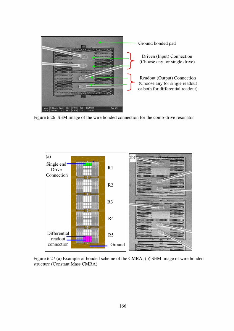
166
Figure 6.26 SEM image of the wire bonded connection for the comb-drive resonator
Figure 6.27 (a) Example of bonded scheme of the CMRA; (b) SEM image of wire bonded
structure (Constant Mass CMRA)
Driven (Input) Connection
(Choose any for single drive)
Readout (Output) Connection
(Choose any for single readout
or both for differential readout)
Ground bonded pad
(b) (a)
Single end
Drive
Connection
Differential
readout
connection Ground
R1
R2
R3
R4
R5

167
The structures were wire bonded by using a Delvotek 6319 Ultrasonic Wire Bonder. The
machine uses an aluminium wire with the wire diameter of 25µm and welded at 60kHz.
Figure 6.26 shows an example of the wire bonded connections for the single comb-drive
resonator (CMRA-v2). Only a single connection is required for the single drive or single
readout scheme and 2 wires bonded are required for the differential scheme. Similar
connections are applied to the coupled resonators depending on the resonators used to drive
and readout the CMRA. Figure 6.27 (a) shows an example of a schematic of wire bonded
connection of the Constant Mass CMRA, where the first resonator is used to drive the
structure and the fifth resonator to measure the output signal of the structure. Figure 6.28
shows example of SEM images of a wire bonded structure of the Staggered Mass CMRA.
Figure 6.28 Schematic and SEM image of wire bonded structure: Staggered Mass CMRA

168
6.8 Material Deposition Using FIB
Figure 6.29 SEM images: (a), (b) The position of the platinum mass deposited on the comb
drive resonator; (c) A mass deposited on R1 of the Constant CMRA; (d) The enlarged view of
the deposited mass (approximate size of 45µm length x 4µm width x 2µm thickness); (e)
Deposited platinum which was milled off from the structure
In order to observe the effect of a mass loading on the frequency response pattern of the
structure, a platinum mass was deposited using Dual beam FIB/SEM system (EDAX DB235).
Specifically, the aims of experiment are:-
(a) (b)
(c) (d)
(e)

169
• To examine the effect of mass loading on the single comb drive resonator
• To examine and compare the uniqueness of the frequency response pattern of the
CMRA sensor structure, the stability of system eigenvectors; and to observe the effect
of manufacturing variation on the performance of the CMRA.
Figure 6.29 (a) and (b) show the position where a platinum mass was deposited on the single
resonator. To examine the uniqueness of the frequency response pattern and to validate the
stability of structure’s system eigenvectors , the platinum was deposited on the first resonator
(R1) and the fifth resonator (R5) separately. The first step, the mass was deposited on the R1
(Figure 6.29(c)). After measuring the frequency response pattern of the CMRA, then the
deposited mass at R1 was milled off and another similar amount of mass was deposited at R5.
Approximately, around 0.2 % mass of the single resonator (7.6 x 10⁻¹²
kg) was deposited on
the structures. The mass was deposited using 550PA ion beam current. Figure 6.29 (d) and
(e) show the enlarged image of the deposited mass and the platinum mass which was milled.
It can be observed that in Figure 6.29 (e) some silicon have been removed instead of milling
the deposited platinum only.
6.9 Summary and Conclusion
This chapter presents and discusses the main issues related to the CMRA fabrication
processes and the process to prepare the structure for the frequency response measurement.
The mask design in Section 6.4 is an important stage to ensure the successful of the CMRA
structure fabrication. The CMRA structure fabrications discussed in Section 6.5 used the
standard bulk micromachining processes. The research presented the processes to fabricate 2
separate devices thickness layer of SOI (5 and 20µm). The thin 5µm Si device only requires a
photo resist mask to etch the structure. While as, the thicker 20µm Si device employed double
mask layers to etch the deeper structure.

170
Due to the nature of the micromachining processes and the constraints of some fabrication
facilities, the fabrications require many considerations and details observations on the
processes step for the successful of the structure fabrication (Section 6.6). Detail care and
attention are very important to ensure the structure is clean from any possibility of defects
during the structure fabrication processes. The processes require special attentions to ensure
any possibilities of source of process variations are eliminated.
As discussed in Section 6.5 and 6.6 the tolerance in manufacturing processes initially
arises from the lithography processes [162]. The evenness of the resist thickness layer, the
exposure and development time have significant impacts on the final profile of the transferred
pattern. Those transferred patterns determined the final geometrical shape and dimensions of
the fabricated CMRA (length, height, width and structure profile). Even though certain source
of the variations are unavoidable (i.e. flatness and smoothness of the hot plate), the CMRA
structures were fabricated to ensure that all the defects are reduced, the structures are able to
be released, and packaged.
Overall, to evaluate the CMRA performance, the three CMRA(s) structures (discussed
in Chapter 5) which include 5 Constant Mass CMRA, 5 Staggered Mass, and 5 Staggered
Stiffness CMRA; the singleton of the CMRA-v2 and CMRA-v1 (the integrated comb-drive
resonator and fixed-fixed beam resonator) were fabricated. To confirm the performance of
the designed CMRA(s), the frequency response of the fabricated structures are then measured
and discussed in Chapter 7. The effect of the manufacturing variation will be observed by
comparing the frequency response of three similar single resonators which were fabricated on
a single chip and the change of the measured frequency response of the CMRA when
comparing with the simulated response.

171
CHAPTER 7 - FREQUENCY RESPONSE MEASUREMENT,
RESULT AND DISCUSSION
7.1 Introduction
This chapter presents and discusses the electronic testing of the fabricated CMRA structure,
the measurement results and the CMRA performance as a sensor. Section 7.2 highlights aims
of the electronic testing. Section 7.3 describes the electronic testing setup and measurement
of the CMRA and its single element. Testing procedures and testing samples are highlighted
in Section 7.4. Section 7.5 presents and discusses the frequency measurement result of the
single resonator (fixed-fixed beam and comb-drive resonator). Performance of the fabricated
CMRA(s) which include Constant Mass CMRA, Staggered Mass CMRA and Staggered
Stiffness CMRA are discussed and compared in Section 7.6. Section 7.7 discusses the
stability of the measured frequency response pattern of the CMRA and its single structure
element. Section 7.8 summarizes and discusses the overall performance of the CMRA sensor
structure.
7.2 Aim of Electronic Testing
The aims of the electronic testing are:-
7.2.1 To evaluate the performance of the single resonator of the CMRA structure with
regard to :
• The effect of input voltage and vacuum pressure level on the resonator frequency response.
• The effect of manufacturing process variations on the frequency response of single
resonators.
• Mass loading – frequency response effect of the single resonator.

172
7.2.2 To measure and evaluate the performance of the three CMRA(s): (1) Constant Mass
CMRA, (2) Staggered Mass CMRA, (3) Staggered Stiffness CMRA, in terms of:-
• Measurability and uniqueness of the frequency response of the CMRA(s) before and after
the structure is perturbed by deposited mass using focus ion beam technology.
• Stability of the CMRA structure eigenvectors, and the effects of manufacturing variations
on performance of the CMRA structures.
• Reliability of the frequency response pattern as a signature for the CMRA sensor structure.
7.3 Electronic Testing Setup and Measurement Scheme
7.3.1 Overview of the Electronic Testing Setup
Figure 7.1 Electronic testing setup for frequency response measurement of CMRA
Figure 7.1 shows the electronic testing setup for the frequency response measurement of the
CMRA and its single resonator. The testing setup consists of:
• Testing board
• Vacuum chamber system (Adixen DRYTEL 1025)
• Digital Pressure Indicator
• Power supply unit (ISO TECH IPS 1125)
Oscilloscope Frequency
Generator
Power
Supply
NI BNC2110
Digital Pressure
Indicator
Vacuum chamber
& testing board

173
• Oscilloscope (100 Ms/sec 20 MHz Oscilloscope (DSO) 400)
• Frequency generator (50 Ms/sec Waveform Generator WW5061)
• NI BNC 2110 connector block [126]
• Personal computer which is equipped with a data acquisition system (DAQ, NI PCI-
6133 [127]) and LabVIEW Signal Express software
Figure 7.2 (a) Vacuum chamber fixed on the testing board; (b) Power supply connection unit
Pressure Regulator
Testing Board
Vacuum chamber fixed
on the board
(a)
Earth
5 V 8 V 11 V (b)

174
Figure 7.3 Schematic diagram of the frequency response measurement system
The testing board is used to mount the chip and to process the output signal of the resonator
sensor structure (note: development of the testing board and overall electronic testing setup
configuration for the frequency response measurement are input from Ross Turnbull, a PhD
student from the Oxford University). The sensitivity limit of the current developed frequency
measurement system is 0.1Hz. The vacuum chamber system is used to pump out and control
Frequency
Generator
Oscilloscope
Amplitude-Frequency
(A-F) curve
5 CMRA
iout
AD620
Signal Processing
System
(Testing Board)
Vi
LM6084
iout
Vj
BNC2110
(Connector
Block)
Computer (equipped with NI PCI-6133 (DAQ))
VOut
Vin
R1 R2 R3 R4 R5
Resonator
(ground)

175
the air pressure level, so that the structure can be tested at a reduced air damping condition.
As shown in Figure 7.2(a), the chamber was fixed onto the measurement board during the
testing process. The digital pressure indicator records the pressure level of the vacuum
chamber system. Figure 7.2(b) shows the power supply unit, which was used to supply the
DC voltage to amplifiers on the testing board (11V and -5V), and the Transimpedance
amplifier (±8V sense voltage) for the readout connections. The oscilloscope was used to
observe the resonant frequency of the measured structure by manually sweeping the
frequency generator. The BNC2110 connector block was employed to interface the input line
(drive pin connection), the output line, and the Data Acquisition System (DAQ) in order to
automatically display the frequency response measurement curve of the measured structure on
the computer screen. Figure 7.3 illustrates a schematic diagram of the CMRA frequency
response measurement system (e.g. CMRA structure with the drive and readout at R1-R5).
7.3.2 Measurement Scheme
Two measurement schemes were used to measure the CMRA and single resonator:-
• Single ended drive – Single readout
• Single ended drive – differential readout
The schemes were selected based upon the design configuration of the structure to be
measured. For example, the fixed-fixed beam resonator employs the single ended drive –
Single readout measurement scheme; while the integrated comb drive-resonator and the three
CMRA(s) structures (5 Constant Mass CMRA, 5 Staggered Mass CMRA, and 5 Staggered
Stiffness CMRA) employ the single ended drive – differential readout measurement scheme
[163]. Figure 7.4 shows the schematic of the wire bonded scheme of the fixed-fixed beam
resonator and the integrated comb drive-resonator structure. The bond pad connected to the

176
fixed comb structure was used to drive and readout the output signal of the resonator; while
the moving structure or resonator was connected to the earth.
Figure 7.4 (a) Single ended drive – single readout measurement scheme for the fixed-fixed
beam resonator; (b) Single ended drive – differential readout measurement scheme for the
integrated comb drive resonator
Single
Ended
Drive
Connection
Ground
Connection
(Resonator)
Differential
Readout
Connection
(b)
Note: Drive pad; Readout pad; Resonator or Ground pad
Single ended
Drive
Connection
Single Readout
connection
Ground Connection
(Resonator)
(a)

177
Figure 7.5 Testing chip mounted on electronic testing board; and example of wiring
connections for single ended drive and differential readout scheme (drive pin: 4, ground pin:
1, readout pin: 23 and 24, output line: Out3)
1 2 3 4 5 6 7 8 9 10 11 12
Drive and Ground
Channel
Connections
(1 – 12)
Testing chip
stuck on
chip carrier
and covered
with
a Plastic lid
Pre-amplify stage (V13-V24);
Readout Connections
(13 – 24);
Final amplify stage (Out1-Out3)
13 14 15 16 17 18 19 20 21 22 23 24
V13 V15
V16
V17
V18
V19
V20
V21
V22
V23
V24
Out 1
Out 2
Out 3
1_V+
2_V+
3_V+
1_V-
2 V-
3_V-
V14
11 V 5 V
Guide line to fix the
vacuum chamber
To Power
Supply
-8V
+8V
Ground
To Earth
(Power Supply)
11V -5V
To Power Supply
Drive connection: to
Frequency generator
Input line (Oscilloscope or BNC 2110)
Output line (Oscilloscope or BNC 2110)
24 to 3_ V+
23 to 3_ V-
LM6084
AD620

178
Figure 7.5 details the testing board, which consists of the drive and ground channel
connections (channel 1 to 12), clamping socket to mount the testing sample, marking line to
fix the vacuum chamber, two power supply connections to feed the amplifiers (11V and -5V
supply voltage), and the readout channel connections (channel 13 to 24). The output signal
processing system comprises Transimpedance amplifiers (LM6084) and Instrumentation
amplifiers (AD620).
As presented earlier in Chapter 3 (Section 3.2.1) and Figure 7.3, due to the different
voltages fed to the fixed driven comb structure and the grounded resonator, an electrostatic
force was generated to vibrate the resonator. The movement of the resonator produces an
output signal in the form of current (iout) at the readout channel. To convert the output current
(iout ) to a useful voltage, ±8V 3DC sense voltage (VDCs) was fed to the Transimpedance
amplifier as illustrated in Figure 7.6. Then the signal is further amplified by the
instrumentation amplifiers, AD620.
Figure 7.6 The schematic of the Transimpedance amplifier used to convert the output signal
of the measured structure (iout) to a useful readout voltage (example for channel 23)
3 Note that the 8V detection bias will slightly affect the effective resonator spring constant (KE = dFel/ dy =
- V2Co/yo). For example with a static capacitance of 1.87 x10
-13 F (Co) at an initial displacement of 5µm (yo),
the change of the effective spring constant of a particular resonator is - 0.4787 N/m when the 8V DC voltage is
applied to the resonator. The change will likely impact the eigenmodes of the CMRA. To ensure a consistent
measurement result it is important to maintain the DC bias voltage for all the device measurement.
-
+
iout
R
VDCs sense voltage
V23 = VDCs + iout R
Ccomb

179
Twelve channels (V13 – V24) configured on the testing board (Figure 7.5) were used to
supply the VDCs sense voltage to the Transimpedance amplifier for the twelve readout
channels (4 x three LM6084 on the testing board). When the differential readout scheme is
used to measure the output signal of the structure, the output of V+ and V- channels (two
connections) of the Transimpedance amplifier were fed to the Instrumentation amplifier,
AD620. If the single readout connection scheme is used, only the output of V+ was fed to the
positive channel of the AD620 and VDCs to the negative channel of the amplifier. Figure 7.7
compares the input and output signal of the AD620 amplifier for the single and differential
readout measurement scheme. Note that G is gain of the instrumentation amplifier (AD620),
dc/dy is the change of capacitance when the resonator moves and dy/dt is the velocity of the
resonator.
Figure 7.7 The input voltage and output of the AD620 amplifier: (a) Single readout
measurement scheme; (b) Differential readout measurement scheme
7.4 Frequency Response Measurement
7.4.1 Testing Procedures
1. After wire bonding the structure and chip connectivity was checked in case there were
short circuits between the 24 pins of the chip carrier.
-
+
Vout = G*(V+ - V-)
= G.R iout
= G.R. VDCs.(dc/dy).(dy/dt)
VDCs
VDCs + iout R
(a)
Vout -
+
VDCs - iout R
VDCs + iout R
(b)
Vout = G*(V+ - V-)
= G.R iout
= 2G.R. VDCs.(dc/dy).(dy/dt)
Vout

180
2. If no short circuit was present, the chip carrier was mounted in the clamping socket on the
testing board. All the connections on the testing board and overall testing setup were
checked (refer to Figure 7.5 as examples of connections on the testing board):
• A driven line (e.g. channel 4) was connected to the frequency generator and an
oscilloscope (manual frequency sweeping) or BNC 2110 connector block (automatic
frequency sweeping). All grounds and resonator line (e.g. channel 1) were connected to
the earth.
• The readout channels (e.g. V23 and V24) were supplied with ±8V DC sense voltage.
• The outputs of pre-amplify stages (channel 23 and 24) were further amplified by
connecting to a final amplify stage channels (e.g. 3_V+ and 3_V-).
• The final output line (i.e. Out3) was connected to the oscilloscope (for manual frequency
sweeping) or to the BNC2110 connector block (for automatic sweeping). (Note: any
lines connected to the substrate of the structure were grounded (to reduce an electrical
effect on the measured Si device layer).
3. The personal computer, frequency generator, digital pressure indicator and vacuum
chamber motor were switched on.
4. When a light indicator of the vacuum system turns to active mode, the vacuum chamber
was fixed onto the testing board. Then, the vacuum system pump was switched on. The
air inside the vacuum chamber was released by turning the pressure regulator until the
digital pressure indicator shows the pressure level at which the frequency response
measurement will be done.
5. Manual frequency sweeping: the power supply unit was switched on. The Vpp voltage
(VAC) of the frequency generator was set in order to drive the measured structure. The
frequency generator was manually swept through the range of natural frequencies of the

181
CMRA structure. The resonant frequency was observed on the oscilloscope when the
sweeping frequency coincides with the natural frequency of the resonator and the peaks
of the sinusoidal output wave become double (Figure 7.8). The range of the frequency
bandwidth was noted (when the peaks of the sinusoidal output wave become double and
back to the original condition).
Figure 7.8 Resonant frequency observed on oscilloscope (output wave become double)
6. Automatic frequency sweeping: the input line and output line were connected to the BNC
2110 connector block. The sweeping parameters (Vpp driving voltage, range of
sweeping frequency bandwidth and sweeping step, input and output frequency filters)
were set on the LabVIEW SignalExpress software window. The frequency response
measurement was started by clicking the ‘Run Once’ button on the menu bar of the
LabVIEW window.
7.4.2 Overview of Testing Samples and Testing Conditions
Table 7-1 List of measured chips and details description of the structure on the chip
Chips Structure Description
Chip1 A single comb drive resonator of the CMRA-v2
Chip2 Three similar single fixed-fixed beam resonators (singleR-v1)
Chip3,Chip4, Chip5
Three similar single comb drive-resonators (singleR-v2)
Chip6, Chip7 5 Constant Mass CMRA
Chip8, Chip9 5 Staggered Mass CMRA
Chip10, Chip11 5 Staggered Stiffness CMRA
Input
Output

182
As listed in Table 7-1, eleven chips which were in-house fabricated were measured which
contained single and coupled resonators. Table 7-2 summarizes all the conducted tests and
testing parameters for the eleven chips.
Table 7-2 Summary of conducted test for eleven chips
Setting Parameter No Conducted Test Chips
Vacuum
Pressure
Level (Pa)
Vpp input
voltage
(V)
230, 36,
1.6, 0.73,
0.1
0.4 1 The effect of vacuum pressure level and
Vpp input voltage on frequency response of
the single resonator
Chip1
0.1 0.1, 0.2, 0.3,
0.4, 0.5, 1, 2
2 Mass loading – frequency response effect
on single resonator (7.6 x 10⁻¹²
kg
perturbed mass)
Chip1 0.1 0.4
Chip2 0.1 5
Chip3 0.1 0.4
Chip4 0.1 0.4
3 The effect of manufacturing variations on
frequency response of the single resonators
Chip5 0.1 0.4
Chip6 0.1 2
Chip7 0.1 2
Chip8 0.1 2
Chip9 0.1 2
Chip10 0.1 2
4 Frequency response of three unperturbed
CMRA(s) structure:
- 5 Constant Mass CMRA (Chip6 and 7)
- 5 Staggered Mass CMRA (Chip 8 and 9)
- 5 Staggered Stiffness CMRA (Chip10,11) Chip11 0.1 2
Chip6 0.1 2
Chip9 0.1 2
5 Uniqueness and the effect of manufacturing
variations on frequency response pattern of
three perturbed CMRA(s) structure
(Note: after mass is perturbed separately
at resonator 1 (R1) and resonator 5 (R5))
Chip11 0.1 2
Chip4 0.1 0.4 6 Reliability of frequency response pattern of
single resonator and CMRA: Comparison
between first and second measurement;
second measurement was done after 49
days for single resonators (Chip4) and after
45 days for CMRA structure (Chip8)
Chip8 0.1 2

183
Six main tests were conducted in order to evaluate the performance of the CMRA and its
singleton. Test no. 1, 2 and 3 were conducted to evaluate the performance of single
resonators. Test no. 4, and 5 were carried out to evaluate the performance of the three
CMRA(s) structures. Test no. 6 observed the reliability and stability of the frequency
response pattern of single resonator and CMRA structure.
When measuring the CMRA structure, several options exist for the drive and readout
point depending on the bonded structure. As discussed in Chapter 5, the selection of the drive
or readout points will not affect the modal eigenfrequencies of the structure, only the response
amplitude of the resonant frequencies will be different. However, the presence of the process
variation may slightly modify the effective mass and stiffness of the coupled resonators or
coupling springs. Driving or readout of CMRA at different points will produce a different
amplitude response. In an extreme case, the response amplitude of the resonant peak may be
very tiny and hard to be observed. To measure the expected 5 resonant peaks of the CMRA
structures, measurements were taken by fixing the drive point to R1, R3 or R5 and the readout
point either at R1 or R5 based on the bonded structure. Unless the resonant peaks were
difficult to measure, the drive and readout point for particular CMRA was not changed to
simplify the structure measurement.
7.5 Result and Discussion 1: Performance of a Single Resonator
7.5.1 Effect of Vacuum Pressure Level
Figure 7.9 presents the frequency response of the single comb-drive resonator at different air
pressure levels. Table 7-3 summarizes the measurement result. Measuring the structure at
different pressure levels slightly shifted the resonant frequency of the resonator. For example,
comparing the measurement at 230 and 0.73 Pa, the shift of frequency is at a maximum of -

184
4.4 Hz (-0.03%). The shift of the frequency is considered small. However, measuring the
structure at a high pressure level drastically decreased the response amplitude and increased
the bandwidth of the measured frequency; hence reducing the Q factor of the resonator.
Comparing the response amplitude at the two measured conditions (230 and 0.73 Pa), the
reduction in amplitude is 95.6%. The decrease of the response amplitude will reduce the
measurability of the frequency response of the measured structure. To ensure measurability
of the frequency response pattern of the single or coupled resonators, all measurements were
made at 0.1 Pa.
Single Resonator (Chip1): 0.4 [V] Vpp Input Voltage &
Varied Vacuum Pressure [Pa]
0.0E+00
4.0E-03
8.0E-03
1.2E-02
1.6E-02
12760 12770 12780 12790 12800 12810 12820 12830 12840
Resonant Frequency [Hz]
Res
po
nse
Am
plitu
de
-
rms
Vo
ut [V
]
230 Pa
36 Pa
1.6 Pa
0.73 Pa
0.1 Pa
Figure 7.9 The effect of different vacuum pressure levels on frequency response pattern of
single resonator
Table 7-3 Summary of the measurement results in Figure 7.9
Vacuum Pressure Level
[Pa]
Resonant Frequency
[Hz]
Response Amplitude
[V]
230 12796.4 5.95 x 10⁻⁴
36 12794.0 3.31 x 10⁻³
1.6 12792.0 1.24 x 10⁻²
0.73 12792.0 1.35 x 10⁻²
0.1 12793.6 1.36 x 10⁻²

185
7.5.2 Effect of Vpp Driving Voltage
Single Resonator (Chip1): 0.1 [Pa] Vacuum Pressure &
Varied Input Vpp [V]
0.0E+00
2.0E-02
4.0E-02
6.0E-02
8.0E-02
1.0E-01
12780 12800 12820 12840 12860
Resonant Frequency [Hz]
Res
po
nse
Am
pli
tud
e -
rm
s V
ou
t [V
]
0.1 V
0.2 V
0.3 V
0.4 V
0.5 V
1 V
2 V
Figure 7.10 The effect of different Vpp input voltage on frequency response pattern of single
resonator
Table 7-4 Summary of the measurement results in Figure 7.10
Input voltage
[V]
Resonant Frequency
[Hz]
Response Amplitude
[V]
0.1 12821.6 7.24 x 10⁻⁴
0.2 12822.0 2.91 x 10⁻³
0.3 12822.0 6.54 x 10⁻³
0.4 12822.0 1.17 x 10⁻²
0.5 12821.6 1.84 x 10⁻²
1 12818.4 4.63 x 10⁻²
2 12806.8 8.53 x 10⁻²
Figure 7.10 displays the frequency response of the comb-drive resonator when measured at
different drive voltages (Vpp). Table 7-4 lists the measured data. At high input voltage (e.g.
2V) the response amplitude of the A-F curve is considerable and the curve is nonlinear.

186
Reducing the input voltage (e.g. 0.4V) reduced the response amplitude to 1.17 x 10⁻²
V, which
is 7 times lower than the amplitude at 2V. Then the measured frequency response curve is
linear.
The cause of the nonlinearity is the electrical spring softening due to the nonlinear
change of capacitance at high input voltage. Equation 3-9 (Section 3.5.2) for the electrostatic
force generated in the resonator (Fel = ½ . δc/δy.V2), Equation 3-10 and 3-11 further can
explain the nonlinear pattern of the measured curve. At high input voltage, the electrostatic
force (Fel) increases and so displaces the resonator. The increase of the resonator
displacement, increases the overlapping distance between the moving and fixed fingers, which
raises rate of the generated capacitance in the structure to nonlinear range (Figure 5.10,
Section 5.3.4 (generated capacitance for the comb-drive resonator)). With a nonlinear
response, the resonant frequency is hard to detect due to the skew of the response curve.
Compared to measurements at 0.4V Vpp, at 2V Vpp the shift of the frequency peak is -15.2
Hz (-0.12%); note that the minus sign indicates the frequency is decreased. To ensure a
consistent and linear frequency response pattern all the measurement of the single comb drive
resonators and the coupled resonators were done at 0.4V Vpp and 2V Vpp respectively. Note
that a phase measurement may be used as an alternative to monitor the nonlinear frequency
response curve.
7.5.3 Effect of Manufacturing Process Variation on a Single Resonator
Figure 7.11 shows the frequency response measurement results of three similar single
resonators from Chip2, Chip3, Chip4 and Chip5. Table 7-5 summarizes the measurement
and data analysis of the result. As can be observed, the measured three resonators on each
chip display different frequency responses. The process variation has significantly modified
the geometrical dimension of the fabricated resonators and altered the response amplitude and

187
resonant frequency of each resonator. If we consider the shift of the resonant frequency of the
comb-drive resonator (Chip3, Chip4 and Chip5), all the measured frequency were larger than
the designed structure (12857.3Hz). The resonator R-1 from Chip3 showed the highest
frequency shift (14076.4 Hz, 9.48%).
Chip2: Fixed-fixed beam R
0.00
0.01
0.02
0.03
21200 21600 22000Resonant Frequency [Hz]
Res
po
nse
Am
pli
tud
e -
rms
Vo
ut
[V]
R-1R-2R-3
Chip3: Comb-drive R
0.000
0.004
0.008
0.012
0.016
0.020
13850 13950 14050 14150Resonant Frequency [Hz]
Res
po
nse
Am
pli
tud
e -
rms
Vo
ut
[V]
R-1R-2R-3
Chip4: Comb-drive R
0.000
0.004
0.008
0.012
0.016
0.020
13200 13400 13600 13800
Resonant Frequency [Hz]
Res
po
nse
Am
pli
tud
e -
rms
Vo
ut [V
]
R-1R-2R-3
Chip5: Comb-drive R
0.000
0.004
0.008
0.012
0.016
13820 13870 13920
Resonant Frequency [Hz]
Res
po
nse
Am
pli
tud
e -
rms
Vo
ut
[V]
R-1R-2R-3
Figure 7.11 Measurement result: (a) three similar fixed-fixed beam resonator fabricated on
Chip2; (b), (c) and (d) three similar integrated comb drive-resonator fabricated on Chip3,
Chip4 and Chip5
(b)
QR-1:10632
QR-2:11358
QR-3:8263
(c)
QR-1:5812
QR-2:7561
QR-3:11352 QR-1:9416
QR-2:9448
QR-3:9804
(a)
QR-2:1815
QR-3:1421
QR-1:1810
(d)

188
Table 7-5 Summary and analysis of results in Figure 7.11
Peak of Resonant Frequency [Hz]
( Response Amplitude [V])
* Percent of frequency shift compared to design value:
(Chip2): 22127.1 [Hz]; (Chip3, 4, 5): 12857.3 [Hz]
** Frequency shift difference (%): resonator frequency shift (%) -
minimum frequency shift (%) on respective chip
Chip (R-1) (R-2) (R-3)
Chip2
21900.0Hz
(2.25 x 10⁻²
V)
* -1.03%
-
21496.0Hz
(2.74 x 10⁻²
V)
* -2.85%
** 1.62%
21364.0Hz
(1.51 x 10⁻²
V)
* -3.45%
** 2.42%
Chip3
14076.4Hz
(1.66 x 10⁻²
V)
* 9.48%
** 1.3%
14056.5Hz
(1.81 x 10⁻²
V)
* 9.33%
** 1.15%
13908.8Hz
(1.27 x 10⁻²
V)
* 8.18%
-
Chip4
13769.2Hz
(9.52 x 10⁻³
V)
* 7.09%
** 3.91%
13660.4Hz
(1.09 x 10⁻²
V)
* 6.25%
** 3.07%
13265.6Hz
(1.82 x 10⁻²
V)
* 3.18%
-
Chip5
13898.4Hz
(1.37 x 10⁻²
V)
* 8.10%
** 0.35%
13899.6Hz
(1.48 x 10⁻²
V)
* 8.11%
** 0.36%
13854.0Hz
(1.45 x 10⁻²
V)
* 7.75%
-
The increase of the measured frequency of the comb drive resonator can be explained by
comparing to the measured geometrical dimension of the comb drive resonator (INTEGRAM
chip) and the estimation of impact of process variation on a single comb-drive resonator
(Appendix G). For particular INTEGRAM resonators, the process variation has increased the
width of the anchor spring and width of the comb finger at about 43.3% and 41.1%
respectively (Section 5.6.1, Table 5-10). By considering a 10% similar increase of width of
the comb finger (bf) and the anchor spring width (bASP), the stiffness of the comb-drive
resonator increases about 33.1% compared to 3.2% increase in resonator mass (Appendix G,
Table G-1). The considerable increase in stiffness compared to the mass, will increase the

189
measured frequency of the comb-drive resonator if we consider the fabricated structure is
oversized. From the sample measurements and data analysis of the manufacturing tolerances
of the in-house fabricated chip (refer to Appendix H (Table H-1, Chip3)), it has been
confirmed that the structures on Chip3 were oversized; the increase of the width of the anchor
springs (bASP) and fingers (bf) were 13.64% and 12.39% respectively. If the maximum
variation on each chip is calculated based on differences between the maximum and minimum
frequency shift of the resonator; the highest variation for each chip was 2.42% (Chip2), 1.3%
(Chip3), 3.91% (Chip4) and 0.36% (Chip5).
Due to the different resonant frequency and response amplitude, each resonator has
different quality factor. The highest quality factor for the fixed-fixed beam resonator and
integrated comb-drive resonator was 1818 and 11358 respectively. The lower Q factor of the
fixed-fixed beam is expected due to the mass and the structure design of the resonator (Q =
mωn/c, Equation 3-8 (Chapter 3)). The mass (m) and frequency of the fixed-fixed beam (ωn)
which was 8 times smaller than the comb drive resonator (designed value) lowered its Q
factor around 6 times. Furthermore, the lower Q of the fixed-fixed beam resonator is
expected due to the loss of resonator energy due to strain at the connection between beam and
anchor pad (clamping force) to support the resonator [76, 164].
7.5.4 Mass Loading Frequency Response Effect of a Single Resonator
Figure 7.12 shows the frequency response of the single comb drive resonator before and after
7.6 x 10⁻¹²
kg platinum was deposited on the structure. The added mass reduced the resonant
frequency and the response amplitude of the resonator by 0.031% and 55.5% respectively.
The perturbation mass significantly increases the effective mass of the resonator (m)
compared to resonator stiffness (k). Hence, reducing the frequency of the resonator, ω (ω =

190
(k/m)1/2
) and the resonant amplitude, x (x = F/(k-mω2). The change of the measured response
was compared to the lumped mass analysis of the designed comb-drive resonator (Figure
7.13). At no damping condition, adding 7.6 x 10⁻¹²
kg mass decreased 0.09% the resonant
frequency and 60.22% response amplitude. Considering some effect of process variations,
the change of the measured frequency response of the perturbed resonator is comparable to
the simulated response. The reduction of the Q factor is expected due to the effect of
aluminium metallization coated on the surface of the resonators which increases the viscous
damping in vacuum [165].
Chip1: 0.4 [V] Vpp and 0.1 [Pa] Chamber Pressure
0.000
0.004
0.008
0.012
12800 12810 12820 12830 12840Resonant Frequency [Hz]
Res
po
nse
Am
plitu
de
rm
s V
out
[V]
Initial condition
Perturbed
response
Figure 7.12 Measurement result: mass loading frequency response effect of single comb-drive
resonator
(12822 Hz; 1.17 x 10⁻²
V)
(12818 Hz; 5.21 x 10⁻³
V)
Q (initial) = 6998
Q (perturbed) = 3384

191
Figure 7.13 Frequency response of unperturbed and perturbed comb-drive resonator (Lumped
mass analysis)
7.6 Result and Discussion 2: Performance of CMRA
The performance of the three CMRA(s) was evaluated by comparing the frequency response
of the designed and the fabricated structure. The uniqueness of frequency response pattern of
the CMRA(s) sensor structure was examined by comparing the response of unperturbed and
perturbed structure (after platinum mass was deposited at R1 and R5 separately). The effect
of manufacturing variation was determined by observing discrepancies between the measured
and simulated frequency response. The inverse eigenvalue analysis was used to estimate the
mass change pattern of the perturbed staggered CMRA(s) and to confirm the stability of the
eigenvectors of the three CMRA(s).
7.6.1 Constant Mass CMRA
7.6.1.1 Frequency Response of the Unperturbed Structure and the Effect of Process Variation
Figure 7.14 and 7.15 present and compare the simulated frequency response and the measured
response of the Constant Mass CMRA fabricated on Chip6 and Chip7 respectively. Table 7-6
summarizes the measured and analyzed data for the structures. For both chips (except for the
12,844 12,848 12,852 12,856 12,8600
0.05
0.1
0.15
0.2
0.25
0.3
Frequency Response of Single Comb-drive Resonator
Frequency [Hz]Res
ponse
Am
pli
tude
[Arb
itra
ry U
nit
]
Initial
+1e-12kg
+7.6e-12kg
Initial:
12857Hz, 0.2979
12845Hz (-0.09%),
0.1185 (-60.22%)

192
mode 5, Chip6), the five measured modal eigenfrequencies were lower than the designed
frequencies which were simulated using FEA. The frequency bandwidth between the first
and fifth resonant peak for the structures was 650.8Hz (Chip6) and 508.8Hz (Chip7)
compared to 467.3Hz for the simulated response.
Figure 7.14 Comparison: frequency response of fabricated Constant Mass CMRA (Chip6) and
simulated response; (a) Simulated response using FEA; (b) Simulated response at varied
resonators stiffness and mass using LMA
1.22 1.24 1.26 1.28 1.3 1.32
x 104
10-7
10-6
10-5
10-4
10-3
10-2
Constant Mass CMRA : Drive-R3, Read-R5
Measured (Chip6) vs Simulated Response
Frequency [Hz]
R
esponse
Am
pli
tude,
log s
cale
Measured
FEA
fM5: 12977.2 fM1: 12326.4
(a)
1.22 1.24 1.26 1.28 1.3 1.32
x 104
10-7
10-6
10-5
10-4
10-3
10-2
10-1
Constant Mass CMRA: Drive-3, Read-5 Measured (Chip6) versus Simulated Response
Frequency [Hz]
Res
ponse
Am
pli
tude,
log s
cale
Measured
LMA
(b)
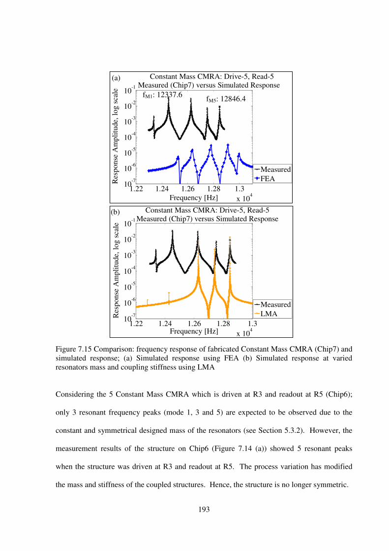
193
Figure 7.15 Comparison: frequency response of fabricated Constant Mass CMRA (Chip7) and
simulated response; (a) Simulated response using FEA (b) Simulated response at varied
resonators mass and coupling stiffness using LMA
Considering the 5 Constant Mass CMRA which is driven at R3 and readout at R5 (Chip6);
only 3 resonant frequency peaks (mode 1, 3 and 5) are expected to be observed due to the
constant and symmetrical designed mass of the resonators (see Section 5.3.2). However, the
measurement results of the structure on Chip6 (Figure 7.14 (a)) showed 5 resonant peaks
when the structure was driven at R3 and readout at R5. The process variation has modified
the mass and stiffness of the coupled structures. Hence, the structure is no longer symmetric.
1.22 1.24 1.26 1.28 1.3
x 104
10-7
10-6
10-5
10-4
10-3
10-2
10-1
Constant Mass CMRA: Drive-5, Read-5 Measured (Chip7) versus Simulated Response
Frequency [Hz]
Res
ponse
Am
pli
tude,
log s
cale
Measured
LMA
1.22 1.24 1.26 1.28 1.3
x 104
10-7
10-6
10-5
10-4
10-3
10-2
10-1
Constant Mass CMRA: Drive-5, Read-5 Measured (Chip7) versus Simulated Response
Frequency [Hz]
Res
ponse
Am
pli
tude,
log s
cale
Measured
FEA
fM1: 12337.6 fM5: 12846.4
(a)
(b)

194
The effect of process variations can be explained by referring to the SEM measurement of the
geometrical dimension of the comb drive resonator from the INTEGRAM chip (as discussed
in Chapter 5 and Section 7.5.3); the decrease in the measured frequencies (Chip6 and Chip7,
Table 7-6) may be expected due to the effect of structure undersized (i.e. some resonators)
which decreases the mass and stiffness of the coupled resonators. Considering at 2.5%
decrease in the width of the resonator anchor spring (bASP) and width of the comb fingers (bf),
the approximate decrease of the comb-drive resonator mass and stiffness is 0.8% and 7.31%
respectively (Appendix G, Table G-1). The change of the mass and stiffness decreases the
resonator frequency around 3.34%.
Table 7-6 Summary and data analysis of unperturbed Constant Mass CMRA (Figure 7.14 and
7.15) m
Measured Frequencies [Hz] ; (Response Amplitude, rms Vout [V]) d
Designed frequencies (FEA)
* Percent (%) of modal frequency shift compared to FEA value
**( ) Normalized % of modal frequency shift (over the maximum value) vVariation (LMA)
Chips/
Analysis
Mode1 Mode2 Mode3 Mode4 Mode5 m
12326.4
(5.62 x 10⁻⁴
)
m12478.4
(2.83 x 10⁻³
)
m12621.2
(3.92 x 10⁻³
)
m12796
(1.93 x 10⁻³
)
m12977.2
(3.43 x 10⁻³
) d12526.8 -
d12776.8 -
d12994.1
*-1.6%
** (-1)
*-1.22%
** (-0.76)
*-0.13%;
** (-0.08)
Chip 6
Drive-R3/
Read-R5
v12349
v12460
v12622
v12814
v12967
m12337.6
(2.18 x 10⁻³
)
m12450.4
(3.65 x 10⁻²
)
m12624.4
(3.05 x 10⁻²
)
m12751.2
(7.35 x 10⁻³
)
m12846.4
(9.73 x 10⁻³
) d12526.8
d12635.7
d12776.8
d12907.1
d12994.1
*-1.51%
** (-1)
*-1.47%
** (-0.97)
*-1.19%
** (-0.79)
*-1.21%
** (-0.8)
*-1.14%
** (-0.76)
Chip7
Drive-R5
Read-R5
v12284
v12432
v12625
v12737
v12842
The same effect of the process variation was considered on the fabricated Constant Mass
CMRA (Chip6) and the lumped mass analysis (LMA) were performed to quantify the effect

195
of the manufacturing variation. As shown in Figure 7.14(b), the analysis produced 5 resonant
peaks, when the mass of the 5 constant coupled resonators (R1, R2, R3, R4 and R5) was
varied by -0.71%, -0.9%, -0.48%, -1.22% and 0.03% respectively. An average error between
the 5 estimated modal eigenfrequencies and the measured frequencies was 0.11% (Table 7-6).
Figure 7.15(b) shows the LMA result of the simulated response for the 5 Constant Mass
CMRA on Chip7 when the mass of the resonators were varied by -1.06% (R1), -1.22% (R2),
and -0.48% (R3, R4, and R5) and stiffness of the 4 constant coupling springs were changed
from 0.2495N/m to 0.22, 0.24,0.20 and 0.23N/m. As can be observed the third and the last
modal frequencies are closely fit to the measured response compared to the modal frequencies
1, 2 and 4. The average errors between the 5 estimated and measured modal eigenfrequencies
was 0.15% (Table 7-6).
From the measured and simulated modal eigenfrequencies of the CMRA on Chip6 and
7, we can emphasize that the process variation has significantly changed the mass of the
coupled resonators. If the structure is to be used as a sensor, it is important to exactly
quantify the change of the resonator mass of the fabricated structure; so that any absorbed
mass onto each resonator can be determined accurately. Optimization techniques such as
Genetic Algorithm may be employed to further analyse and incorporate multi-parameters
change of mass, stiffness and frequency response of the couple resonators [166-168] due to
the effect of manufacturing variations.
7.6.1.2 Uniqueness of the Frequency Response - Constant Mass CMRA
Figure 7.16 compares the frequency response pattern of the Constant Mass CMRA structure
when a mass was perturbed at R1 and R5 separately. For both perturbed conditions, a unique
frequency response pattern were observed. Table 7-7 summarizes the measured data.

196
Figure 7.16 Comparison: frequency response pattern of unperturbed and perturbed Constant
Mass CMRA
Table 7-7 Summary of measurement data (Figure 7.16) and data analysis
Modal Frequencies, fM [Hz]
(Response Amplitude, rms Vout [V])
Note:- Frequency and amplitude difference =
perturbed value – initial value
Measurement
/ Analysis
Chip6
Mode1 Mode2 Mode3 Mode4 Mode5
Initial
12326.4
(5.62 x 10⁻⁴
)
12478.4
(2.83 x 10⁻³
)
12621.2
(3.92 x 10⁻³
)
12796
(1.93 x 10⁻³
)
12977.2
(3.43 x 10⁻³
)
+m at R1 12264.4
(4.25 x 10⁻⁴
)
12462.8
(1.95 x 10⁻³
)
12599.6
(3.84 x 10⁻³
)
12784.4
(2.18 x 10⁻³
)
12971.6
(3.11 x 10⁻³
)
Frequency
difference
-62
-0.50%
-15.6
-0.13%
-21.6
-0.17%
-11.6
-0.09%
-5.6
-0.04%
Amplitude
difference
-1.37 x 10⁻⁴
,
-24.38%
-8.8 x 10⁻⁴
,
-31.1%
-8.0 x 10⁻⁵
,
-2.04%
2.5 x 10⁻⁴
,
12.4%
-3.2 x 10⁻⁴
,
-0.09%
+m at R5
12225.6
(3.05 x 10⁻³
)
- 12577.2
(6.5 x 10⁻³
)
- 12925.6
(4.04 x 10⁻³
)
Frequency
difference
-100.8
-0.82%
- -44.0
-0.35%
- -51.6
-0.4%
Amplitude
difference
2.5 x 10⁻³
444.8%
- 2.6 x 10⁻³
66.33%
- 6.1 x 10⁻⁴
17.78%
1.22 1.24 1.26 1.28 1.3
x 104
0
1
2
3
4
5
6
7x 10
-3
Constant Mass CMRA (Chip6):Frequency Response of Unperturbed and Perturbed Structure
Frequency [Hz]
Res
po
nse
Am
pli
tud
e [R
MS
Vo
ut]
initial
+m@R1
+m@R5

197
Table 7-8 Eigenvalue analysis result of Constant Mass CMRA (ideal condition) using lumped
mass analysis (7.6 x 10⁻¹²
kg mass was perturbed at R1 and R5 separately)
Analysis f(mode1) f(mode2) f(mode3) f(mode4) f(mode5)
Initial [Hz] 12857 12888 12968 13066 13144
+m at R1 [Hz] 12853 12882 12964 13064 13144
+m at R5 [Hz] 12853 12882 12964 13064 13144
The perturbation mass at R1 reduced the 5 unperturbed modal frequencies. The highest and
lowest frequency shift occurred at mode1 and mode 5 (Table 7-7). After the deposited mass
at R1 was milled off and 7.6 x 10⁻¹²
kg platinum mass was deposited at R5, the measurement
result shows only 3 resonant peaks (mode1, 3 and 5). It can be claimed that, the variation in
the milling process (i.e. a slight over milled the silicon material (see Section 6.8)), and the
perturbation mass at R5 have balanced the masses discrepancy between R1 and R5; hence 3
resonant peaks were produced when driving and measuring the structure at R3 and R5.
The frequency response pattern of the measured structure may be further explained by
referring to the eigenvalue analysis result of the designed structure (Table 7-8 and Section
5.4.2, Chapter 5). Due to the symmetrical designed mass of the resonators, similar resonant
frequencies shift were produced when adding mass at R1 or R5. In contrast, the fabricated
structure (Chip6) showed unique frequency response patterns when platinum mass was
perturbed separately at R1 and R5. Hence, the process variation has evidently staggered some
mass and stiffness of the designed constant mass coupled resonators as discussed in Section
7.6.1.1. The variation of the perturbation mass deposited at R1 and R5 also affected the
frequency response pattern of the measured structure. As a result the Constant Mass CMRA
(Chip6) produced a unique frequency response pattern for a single perturbed resonator sensor
(i.e. for R1and R5).

198
7.6.1.3 Stability of the Structure Eigenvectors
To confirm the stability of system eigenvectors between the designed and the fabricated
structure, the inverse eigenvalue analysis was considered (refer to Section 5.5). The designed
eigenvectors and the measured eigenvalues were used to determine the mass change pattern of
the unperturbed and perturbed structure. Figure 7.17(a) shows the inverse eigenvalue analysis
result of the structure on Chip6 before and after a mass was perturbed at R1. As expected, the
perturbed eigenvectors of the Constant Mass CMRA are always unstable compared to the
unperturbed designed structure. Using the designed eigenvectors to estimate the mass change
pattern of the resonators always cause errors; i.e. the estimated mass for R1 always mirrors
the estimated mass at R5 when mass only perturbed at R1 (Figure 7.17(b)) . It is interesting
to further research a new set of the unperturbed eigenvectors of the fabricated structure. We
then can confirm how the process variation may naturally stabilize the structure eigenvectors;
and estimate the mass change pattern of the perturbed structure using inverse eigenvalue
analysis.
Figure 7.17 (a) Estimation of mass of unperturbed and perturbed Constant Mass CMRA
(Chip6) using Inverse Eigenvalue Analysis; (b) Mass change pattern of structure (perturbed
mass at R1)
1 2 3 4 53.2
3.225
3.25
3.275
3.3x 10⁻⁹
5 Constant Mass CMRA (Chip6): Estimated Mass -Inverse Eigenvalue Analysis
Resonator 1 to 5
Mas
s [K
g]
Initial
+m@R1
(a)
1 2 3 4 51.1
1.2
1.3
1.4x 10⁻¹¹
Estimated Mass Change Pattern of
Constant Mass CMRA(Chip6):
+7.6e-12kg at R1)
Resonator 1 to 5
Mas
s [K
g]
(b)

199
7.6.2 Staggered Mass CMRA
7.6.2.1 Frequency Response of the Unperturbed Structure and the Effect of Process Variation
Figure 7.18 presents and compares the measured frequency response of the 5 Staggered Mass
CMRA from Chip8 and Chip9 and the simulated response from FEA. The frequency
bandwidth between the first and fifth peaks for both structures are 502.2Hz (Chip8) and
647.2Hz (Chip9); while the simulated modal frequencies bandwidth is 508.4Hz. Table 7-9
details the measured and simulated responses.
Figure 7.18 Comparison: frequency response of fabricated Staggered Mass CMRA and
Simulated response (FEA); (a) Chip8; (b) Chip9
1.22 1.24 1.26 1.28 1.3 1.32
x 104
10-7
10-6
10-5
10-4
10-3
10-2
10-1
Frequency [Hz]
Res
po
nse
Am
pli
tude,
lo
g s
cale
Staggered Mass CMRA : Drive-R1,Read-R1
Measured (Chip8) vs Simulated Response
Measured
FEA
(a)
fM1: 12627.2
fM5: 13129.4
1.22 1.24 1.26 1.28 1.3
x 104
10-7
10-6
10-5
10-4
10-3
10-2
Staggered Mass CMRA : Drive-R1, Readout-R5Measured (Chip9) vs Simulated Response
Frequency [Hz]
Res
po
nse
Am
pli
tud
e, l
og
sca
le
Measured
FEA
fM5: 12904.0
fM1: 12256.8
(b)

200
Considering the structure on Chip8 (Figure 7.18(a)), the measured 5 modal frequencies are
higher compared to the simulated eigenfrequencies (Table 7-9). We may expect that the
structure is slightly oversized; the increase in stiffness of the resonators is higher than the
increase in mass of the structure, when the process variation altered the geometrical
dimension of the structure. Therefore, the measured eigenfrequencies are higher than the
simulated response. From the sample measurements and data analysis of the manufacturing
tolerances on Chip8 have confirmed that the structures were oversized (refer to Appendix H
(Table H-2)); the increase of the width of the anchor springs (bASP) and fingers (bf) were
6.51% and 5.78% respectively. The variation has affected the Staggered Mass CMRA on
Chip9 differently. The first four measured modal frequencies are lower compared to the
simulated response, but the last modal frequency is higher compared to the simulated
eigenfrequency. Hence, we may expect that some of the coupled structures are slightly
undersized, which reduces the measured modal frequencies; and some resonators are
oversized.
Table 7-9 Summary of the measurement results of unperturbed Staggered Mass CMRA
m
Measured Frequencies [Hz] ; (Response Amplitude, rms Vout [V]) d
Designed frequencies (FEA)
* Percent (%) of modal frequency shift compared to FEA value
**( ) Normalized % of modal frequency shift (over the maximum value)
Chips
Mode1 Mode2 Mode3 Mode4 Mode5
m12627.2
(3.9 x 10⁻³
)
m12702.8
(3.81 x 10⁻³
)
m12852.8
(2.13 x 10⁻²
)
m13038.8
(3.51 x 10⁻²
)
m13129.4
(5.06 x 10⁻³
) d 12322.9
d 12485.1
d 12621.0
d 12789.0
d 12831.3
Chip8
Drive-R1/
Readout-R1
* 2.47%
**(1)
* 1.74%
**(0.70)
*1.84%
**(0.74)
* 1.95%
**(0.79)
* 2.32%
**(0.94) m
12256.8
(5.57 x 10⁻⁴
)
m12451.2
(5.11 x 10⁻³
)
m12583.6
(8.23 x 10⁻³
)
m12702.0
(5.88 x 10⁻³
)
m12904.0
(9.81 x 10⁻⁴
) d 12322.9
d 12485.1
d 12621.0
d 12789.0
d 12831.3
Chip9
Drive-R1/
Readout-R5
* -0.54%
**(-0.79)
* -0.27%
**(-0.40)
* -0.3%
**(-0.44)
* -0.68%
**(-1)
* 0.57%
**(0.84)

201
Figure 7.19 Comparison: designed mass and estimated mass of Staggered Mass resonators
(using inverse eigenvalue analysis); (a) Chip8; (b) Chip9; (c) Designed mass and estimated
mass from the FEA simulated response
Table 7-10 Staggered Mass CMRA: comparison- designed mass and estimated mass of the
fabricated structure using inverse eigenvalue analysis
Resonator(R) R1 R2 R3 R4 R5
Designed Mass nanokg] 3.0941 3.1932 3.2241 3.1616 3.1263
Chip8: Estimated Mass
[nanokg]
3.049
(-1.46%)
3.175
(-0.57%)
3.211
(-0.41%)
3.127
(-1.09%)
3.106
(-0.65%)
Chip9:Estimated Mass:
[nanokg]
3.189
(3.07%)
3.324
(4.10%)
3.379
(4.80%)
3.269
(3.40%)
3.242
(3.70%)
The discrepancies between the fabricated and the designed structure was further analysed by
considering the inverse eigenvalue analysis (IEA) to approximately quantify the mass change
1 2 3 4 53
3.1
3.2
3.3
3.4x 10⁻⁹
5 Staggered Mass CMRA (Chip9):
Estimated Mass -Inverse Eigenvalue Analysis
Resonator 1 to 5
Mas
s [K
g]
Designed
Chip9
(a) (b)
1 2 3 4 53
3.1
3.2
x 10-9
5 Staggered Mass CMRA (Chip8):
Estimated Mass-Inverse Eigenvalue Analysis
Resonator 1 to 5
Mas
s [K
g]
Designed
Chip8
(c)
1 2 3 4 53.08
3.12
3.16
3.2
3.24x 10
-9
Staggered Mass CMRA: Designed Vs Estimated Mass-FEA Response (IEA)
Resonator 1 to 5
Des
igned
Mas
s [k
g]
Designed
1 2 3 4 5
3.2
3.25
3.3
3.35
3.4x 10
-9
Resonator 1 to 5
Est
imat
ed M
ass
[kg]
FEA(IEA)

202
of the fabricated coupled resonators. Figure 7.19 displays the analysis result and Table 7-10
summarizes the data. By assuming a small change in the stiffness of the resonator, the
estimated mass for the 5 resonators on Chip8 are lower than the designed mass (Figure
7.19(a)). The maximum mass change is -1.46% for R1. While the estimated masses for the
structure on Chip9 are higher than the designed mass, with the maximum mass change is
4.80% for R3 (Figure 7.19(b)). Figure 7.19(c) shows the comparison between the designed
mass of the coupled resonators and the estimated mass (using IEA) of the FEA simulated
response (see Figure 7.18(a)). Considering the differences of the resonator mass in Figure
7.19(c); and comparing between the modal frequency bandwidth for the structure on Chip8
(502.2Hz), Chip9 (647.2Hz) and the simulated response (508.4Hz), the estimated masses for
both fabricated structure is considered sensible at no or small change in the resonator
stiffness.
alculating the differences between the maximum and minimum change of mass; the
maximum mass variation estimated for both structure are 1.05% (Chip8) and 1.73% (Chip9).
As exemplified by the Chip8 and Chip9, the manufacturing variation may affect the fabricated
CMRA differently. Therefore, a calibration is important for each fabricated CMRA to exactly
quantify the change of the mass, before the structure can be used as a sensor.
7.6.2.2 Uniqueness of the Frequency Response - Staggered Mass CMRA
Figure 7.20 shows comparison of the frequency response pattern of the unperturbed Staggered
Mass CMRA and after mass was perturbed at R1 and R5 separately. As can be observed,
each single perturbed resonator (R1 and R5) produced a unique frequency response pattern to
present a signature for that particular resonator sensor.

203
Figure 7.20 Comparison: frequency response pattern of unperturbed and perturbed Staggered
Mass CMRA
Table 7-11 Summary of measurement result (Figure 7.20) and data analysis
Modal Frequencies, fM [Hz]
(Response Amplitude, rms Vout [V])
Note:- Frequency and amplitude difference =
perturbed value –initial value
Measurement
/ Analysis
Chip9
Mode1 Mode2 Mode3 Mode4 Mode5
Initial
measurement
12256.8
(5.57 x 10⁻⁴
)
12451.2
(5.11 x 10⁻³
)
12583.6
(8.23 x 10⁻³
)
12702.0
(5.88 x 10⁻³
)
12904.0
(9.81 x 10⁻⁴
)
+m at R1 -
12422.8
(1.67 x 10⁻³
)
12541.6
(4.75 x 10⁻³
)
12662.8
(5.1 x 10⁻³
)
12922.8
(1.43 x 10⁻³
)
Frequency
difference -
-28.4
-0.23%
-42
-0.33%
-39.2
-0.31%
18.8
0.15%
Amplitude
difference -
-3.44 x 10⁻³
-67.3%
-3.48 x 10⁻³
-42.3%
-7.8 x 10⁻⁴
-13.3%
4.49 x 10⁻⁴
45.77%
+m at R5
12316.4
(6.76 x 10⁻⁴
)
12522.4
(5.49 x 10⁻³
)
12596.0
(6.6 x 10⁻³
)
12896.0
(2.14 x 10⁻³
)
13048.4
(8.3 x 10⁻⁴
)
Frequency
difference
59.6
0.49%
71.2
0.57%
12.4
0.1%
194
1.53%
144.4
1.1%
Amplitude
difference
1.19 x 10⁻⁴
21.4%
3.8 x 10⁻⁴
7.4%
-1.63 x 10⁻³
-19.8%
-3.74 x 10⁻³
-63.6%
-1.51 x 10⁻⁴
-15.4%
1.22 1.24 1.26 1.28 1.3
x 104
0
1.5
2.5
3.5
4.5
5.5
6.5
7.5
8.5x 10
-3
Staggered Mass CMRA (Chip9):Frequency Response of Unperturbed and Perturbed Structure
Frequency [Hz]
Res
po
nse
Am
pli
tud
e [r
ms
Vo
ut]
initial
+m@R1
+m@R5

204
When an approximate 7.6 x 10⁻¹²
kg mass was added at R1, the measured structure shows only
4 resonant peaks. The missing peak is associated to the response of mode 1. Considering the
mode 4 with the least reduction in the response amplitude (7.8 x 10⁻⁴
V, Table 7-11); the mass is
considerably large to reduce the response amplitude of the first resonant peak (i.e. mode 1)
which is initially 5.57 x 10⁻⁴
V.
When the deposited mass at R1 was milled off and a mass was deposited at R5, five
resonant peaks are observed. It can be argued that the removal mass at R1 significantly
reduces the mass of the structure; hence increases response amplitude of mode 1 and the 5
measured modal frequencies after mass was added at R5 (the resonant frequency, ω = (k/m)1/2
and the response amplitude, x = F/(k-mω2)) . As discussed in Chapter 6, some silicon (R1)
also has been milled instead of removing only platinum. Furthermore, considering the lumped
analysis result of the designed structure (Table 7-12); due to the staggered mass design the
analysis produced unique modal frequencies when mass was perturbed at R1 and R5.
Table 7-12 Eigenvalue analysis result of Staggered Mass CMRA (ideal condition) using
lumped mass analysis (7.6 x 10⁻¹²
kg mass was perturbed at R1 and R5 separately)
Analysis
Mode1 Mode2 Mode3 Mode4 Mode5
Initial [Hz] 12651 12750 12809 12917 12945
+m at R1[Hz] 12650 12748 12806 12911 12942
+m at R5 [Hz] 12650 12744 12804 12915 12943
Overall, the staggered mass design of the coupled resonators and the altered mass due to the
effect of process variations have helped to stagger the structure to produce unique frequency
response pattern for single resonator sensors.

205
7.6.2.3 Stability of the Structure Eigenvectors
Figure 7.21 (a) compares the inverse eigenvalue analysis result of the unperturbed structure
and after mass was perturbed at R5. Note that the mass change pattern of the perturbed R1 can
not be estimated using the inverse eigenvalue analysis since only 4 modal eigenfrequencies
are available (Table 7-11). The 7.6 x10⁻¹²
kg mass used to validate the mass change pattern of
the perturbed R5 in Figure 7.21(b) confirmed that the unperturbed eigenvectors are unstable
to accurately determine the mass change pattern of the resonator. The mass variation effect
(i.e. maximum of 1.73% for Chip9) and the 7.6 x10⁻¹²
kg deposited mass have affected the
stability of the structure eigenvectors; the designed eigenvectors were no more comparable to
estimate the mass change pattern of the fabricated structure when mass was deposited at R5.
Figure 7.21 (a) Estimation of mass of Staggered Mass CMRA (Chip9) using Inverse
Eigenvalue Analysis; (b) Mass change pattern of the perturbed structure
7.6.3 Staggered Stiffness CMRA
7.6.3.1 Frequency Response of the Unperturbed Structure and the Effect of Process Variation
Figure 7.22 presents the measurement result of the unperturbed Staggered Stiffness CMRA
which was fabricated on Chip10 and Chip11. The modal frequency bandwidth between the
1 2 3 4 53.1
3.2
3.3
3.4x 10⁻⁹
5 Staggered Mass CMRA (Chip9):
Estimated Mass -Inverse Eigenvalue Analysis
Resonator 1 to 5
Mas
s [K
g]
Initial
+m@R5
1 2 3 4 53
4
5
66.5x 10
-11
Estimated Mass Change pattern of Staggered Mass CMRA (Chip9):
+7.6e-12kg at R5
Resonator 1 to 5
Mas
s [K
g]
(a) (b)

206
first and fifth resonant peak of the structure is 679.2Hz (Chip10) and 644Hz (Chip11); while
the simulated frequency bandwidth is 502.6Hz. Table 7-13 summarizes the measured data.
Figure 7.22 Comparison: frequency response of fabricated Staggered Stiffness CMRA and
Simulated response (FEA); (a) Chip10; (b) Chip11
12,500 13,500 14,500 15,500
10-6
10-5
10-4
10-3
10-2
Staggered Stiffness CMRA : Drive-R3,Read-R1 Measured (Chip10)vs Simulated Response
Frequency [Hz]
Res
pon
se A
mp
litu
de,
log s
cale
Measured
FEA
(a)
fM5: 15598.8
fM1: 14919.6
12,500 13,000 13,500 14,000 14,500
10-6
10-5
10-4
10-3
10-2
Staggered Stiffness CMRA : Drive-R3,Read-R1 Measured (Chip11)vs Simulated Response
Frequency [Hz]
Res
ponse
Am
pli
tude,
log s
cale
Measured
FEA
fM1: 13710.4
fM5: 14354.4
(b)

207
Table 7-13 Summary of the measurement results of unperturbed Staggered Stiffness CMRA
(Figure 7.22) m
Measured Frequencies [Hz] ; (Response Amplitude, rms Vout [V]) d
Designed frequencies (FEA)
*Percent (%) of modal frequency shift compared to FEA value
**( ) Normalized % of modal frequency shift (over the maximum value)
Chips
Mode1 Mode2 Mode3 Mode4 Mode5 m
14919.6
(1.65 x 10⁻³
)
m15104.0
(1.21 x 10⁻²
)
m15254.4
(1.34 x 10⁻²
)
m15434.4
(4.76 x 10⁻³
)
m15598.8
(5.86 x 10⁻³
) d
12557.9 d
12709.4 d12858.7
d13015.9
d13060.5
Chip10
Drive-R3/
Readout-R1
*18.81%
**(0.97)
*18.84%
**(0.97)
*18.63%
**(0.96)
*18.58%
**(0.96)
*19.43%
**(1) m
13710.4
(6.21 x 10⁻³
)
m13801.6
(8.54 x 10⁻³
)
m13932.0
(1.64 x 10⁻²
)
m14110.4
(6.62 x 10⁻³
)
m14354.4
(8.8 x 10⁻³
) d
12557.9 d
12709.4 d12858.7
d13015.9
d13060.5
Chip11
Drive-R3/
Readout-R1
* 9.18%
**(0.93)
* 8.59%
**(0.87)
* 8.35%
**(0.84)
* 8.41%
**(0.85)
* 9.91%
**(1)
Comparing the measured and simulated responses, since the measured modal frequencies are
much higher than the simulated response, we can expect that both fabricated structures are
oversized due to the effect of process variation. If we consider the increase of the width of
anchor spring, bASP is similar as the increase of the comb finger width, bf (comparing to the
observed INTEGRAM chip), the increase of the resonator stiffness will be much higher than
the increase of mass (i.e. from estimation of the stiffness of an anchor spring, k =
Eh(bASP)3/(LASP)
3 (Equation F-2, Appendix F)) . The effect of change of the stiffness compared
to resonator mass is more significant for the Staggered Stiffness CMRA, since length of the
resonator anchor springs were staggered. Hence, we observe the measured modal frequencies
are higher than the simulated response. The sample measurements and data analysis of the
manufacturing tolerances on Chip10 (refer to Appendix H (Table H-3)) have confirmed that
the structures on the chip were oversized, with 25.59% and 26.6% increase of the width of
the anchor springs (bASP) and fingers (bf).

208
The effect of over-sizing due to the process variation was further analysed using the inverse
eigenvalue analysis to estimate the mass change of the fabricated structure. Figure 7.23
displays the analysis result and Table 7-14 summarizes the estimated mass. Comparing the
estimated masses and the designed mass (at no change of the structure stiffness), the highest
differences for both structures are -27.20% (Chip10, R5) and -13.32% (Chip11, R2). If the
variation for the structure is calculated based on differences between the maximum and
minimum change of the resonator mass, the maximum variations for Chip10 and Chip11 are
0.76% and 0.93%.
Figure 7.23 Comparison: designed mass and estimated mass of Staggered Stiffness CMRA
(using inverse eigenvalue analysis); (a) Designed mass; (b) Chip10; (c) Chip11
0 1 2 3 4 53.057
3.058
3.059
3.06
3.061
3.062x 10⁻⁹
5 Staggered Stiffness CMRA: Designed Mass
Resonator 1 to 5
Mas
s [k
g]
(a)
1 2 3 4 52.225
2.235
2.245
2.255x 10⁻⁹
5 Staggered Stiffness CMRA (Chip10): Estimated Mass-Inverse Eigenvalue Analysis
Resonator 1 to 5
Mas
s [k
g]
(b)
1 2 3 4 52.65
2.66
2.67
2.68
x 10-9
5 Staggered Stiffness CMRA (Chip11):
Estimated Mass-Inverse Eigenvalue Analysis
Resonator 1 to 5
Mas
s [k
g]
(c)

209
Table 7-14 Staggered Stiffness CMRA: comparison- designed mass and estimated mass of the
fabricated structure using inverse eigenvalue analysis
Resonator(R) R1 R2 R3 R4 R5
Designed Mass nanokg] 3.0590 3.0596 3.0615 3.0607 3.0575
Chip10: Estimated Mass
[nanokg]
2.242
(-26.71%)
2.229
(-27.15%)
2.252
(-26.44%)
2.249
(-26.52%)
2.226
(-27.20%)
Chip11:Estimated Mass:
[nanokg]
2.680
(-12.39%)
2.652
(-13.32%)
2.676
(-12.59%)
2.677
(-12.54%)
2.658
(-13.07%)
7.6.3.2 Uniqueness of the Frequency Response - Staggered Stiffness CMRA
Figure 7.24 Comparison: frequency response pattern of unperturbed and perturbed Staggered
Stiffness CMRA
Figure 7.24 compares the measured frequency response pattern of the unperturbed and
perturbed Staggered Stiffness CMRA structure (Chip11). Overall, the measured perturbed
responses are unique. However, the shift of some modal frequencies for both perturbed
conditions (i.e. mode 1, 3 and mode 4) are more or less similar. Table 7-15 summarizes the
measured and analyzed data of the structure.
1.37 1.38 1.39 1.4 1.41 1.42 1.43 1.44
x 104
0
0.004
0.008
0.012
0.016
0.02
Staggered Stiffness CMRA (Chip11):Frequency Response of Unperturbed and Perturbed Structure
Frequency [Hz]
Res
po
nse
Am
pli
tud
e [r
ms
Vo
ut]
initial
+m@R1
+m@R5

210
To understand the effect of mass loading on the frequency response pattern of the Staggered
Stiffness CMRA and the effect of process variation on the fabricated structure, the eigenvalue
analysis result of the designed structure was considered (Table 7-16). Due to the staggered
stiffness design, the shift of modal frequencies for mode 1 is similar and mode 3, and 5 are
almost similar when mass is perturbed at R1 and R5. Considering the measured responses
(Table 7-15), three modal eigenfrequencies (mode 1, 3 and 4) are nearly similar when mass
was perturbed at R1 and R5. The differences of the three frequencies are 2.4Hz (mode1),
1.6Hz (mode 3), and 2.4Hz (mode4). Comparing the measured (Table 7-15) and the designed
modal frequencies (Table 7-16), it can be argued that the impact of process variation is
slightly affected the modal frequency of mode 4 and 5. The mass changes of the structure due
to process variation (as discussed in Section 7.6.3.1) has slightly reduced the
distinguishability of the frequency shift of mode 4 and significantly increased the frequency
shift of mode 5.
Table 7-15 Summary of measurement data (Figure 7.24) and data analysis
Modal Frequencies, fM [Hz]
(Response Amplitude, rms Vout [V])
Note:- Frequency and amplitude difference =
perturbed value – initial value
Measurement
/ Analysis
Chip11
Mode1 Mode2 Mode3 Mode4 Mode5
Initial
measurement
13710.4
(6.21 x 10⁻³
)
13801.6
(8.54 x 10⁻³
)
13932.0
(1.64 x 10⁻²
)
14110.4
(6.62 x 10⁻³
)
14354.4
(8.8 x 10⁻³
)
+m at R1 13698.0
(1.28 x 10⁻²
)
13754.4
(1.9 x 10⁻³
)
13921.2
(1.63 x 10⁻²
)
14099.2
(8.19 x 10⁻³
)
14355.6
(1.12 x 10⁻²
)
Frequency
difference
-12.4
-0.09%
-47.2
-0.34%
-10.8
-0.08%
-11.2
-0.08%
1.2
0.01%
Amplitude
difference
6.6 x 10⁻³
,
106.3%
-6.6 x 10⁻³
-77.8%
-1 x 10⁻⁴
-0.61%
1.57 x 10⁻³
23.7%
2.4 x 10⁻³
27.3%
+m at R5
13700.4
(2.1 x 10⁻²
)
13739.2
(7.21 x 10⁻³
)
13919.6
(1.59 x 10⁻²
)
14101.6
(7.64 x 10⁻³
)
14337.6
(1.09 x 10⁻²
)
Frequency
difference
-10
-0.07%
-62.4
-0.45%
-12.4
-0.09%
-8.8
-0.06%
-16.8
-0.12%
Amplitude
difference
1.48 x 10⁻²
,
238.3%
-1.3 x 10⁻³
,
-15.2%
-5.0 x 10⁻⁴
,
-3.1%
1.02 x 10⁻³
,
15.4%
2.1 x 10⁻³
23.9%

211
Table 7-16 Eigenvalue analysis result of Staggered Stiffness CMRA (ideal condition) using
lumped mass analysis (7.6 x 10⁻¹²
kg mass was perturbed at R1 and R5 separately)
Analysis Mode1 Mode2 Mode3 Mode4 Mode5
Initial (Hz) 12903 12982 13053 13152 13189
+m at R1(Hz) 12902 12975 13048 13150 13188
+m at R5 (Hz) 12902 12980 13049 13144 13187
7.6.3.3 Stability of the Structure Eigenvectors
Figure 7.25 (a) Comparison – Estimated mass of unperturbed and perturbed Staggered
Stiffness CMRA (Chip11) using Inverse Eigenvalue Analysis; (b) Mass change pattern of the
structure (mass perturbed at R1); (c) Mass change pattern of the structure (mass perturbed at
R5)
Figure 7.25 (a) compares the estimated mass of the coupled resonators for the unperturbed
and perturbed structure using the inverse eigenvalue analysis. Comparing between the
unperturbed mass and when structure was perturbed at R1 (Figure 7.25(b)), the analysis
shows that the maximum mass changes is at R1. However, the analysis also shows that the
1 2 3 4 52.65
2.66
2.67
2.68
2.69
2.7x 10⁻⁹
Staggered Stiffness CMRA (Chip11): Estimated Mass- Inverse Eigenvalue Analysis
Resonator 1 to 5
Mas
s [k
g]
Initial
+m@R1
+m@R5
1 2 3 4 53
5
7
9
x 10-12
Estimated Mass Change Pattern of Staggered Stiffness CMRA (Chip11):
+7.6e-12kg at R1
Resonator 1 to 5
Mas
s [k
g]
1 2 3 4 54
8
12
x 10-12
Estimated Mass Change Pattern of
Staggered Stiffness CMRA (Chip11):
+7.6e-12kg at R5
Resonator 1 to 5
Mas
s [k
g]
(a)
(b) (c)

212
maximum mass change at R1 when mass was perturbed at R5 (Figure 7.25(c)). Therefore, it
can argue that the eigenvectors of the fabricated structure are remained stable when 7.6 x10-
12kg mass was perturbed at R1 (i.e. agreeable with modelling analysis (Chapter 5)). Hence,
the analysis using the designed eigenvectors correctly identified the mass change pattern of
the resonator. The effect of process variation and when mass was milled off at R1 caused the
eigenvectors of the fabricated structure were no more stable compared to the designed
eigenvectors. The inverse eigenvalue analysis causes error when using the designed
eigenvectors to estimate the perturbed mass at R5.
7.7 Stability of the Measured Response
Three similar Single Resonators fabricated on a chip (Chip4)
0.0E+00
4.0E-03
8.0E-03
1.2E-02
1.6E-02
2.0E-02
2.4E-02
13200 13300 13400 13500 13600 13700 13800
Resonant Frequency [Hz]
Res
po
nse
Am
pli
tud
e -
rms
Vo
ut
[V]
R-1R-2R-3R-1 (after 49 days)R-2 (after 49 days)R-3 (after 49 days)
Figure 7.26 Measurement result: frequency response comparison of Single resonators
(second measurement: 49 days after the first measurement)
(QR-1:5812)1
(QR-2:7561)1
(QR-3:11352)1 (QR-1:9161)2
(QR-2:4282)2
(QR-3:10608)2

213
The stability of the measured frequency response pattern was examined by comparing
between the first and second batch of the measurements. Figure 7.26 displays and compares
the frequency response of three single comb-drive resonators (Chip4) between the first and
second measurement. Table 7-17 details the measurement result.
Table 7-17 Summary of data analysis of measured structure (Figure 7.26)
Peak of Resonant Frequency [Hz]
( Response Amplitude [V])
Differences = Measurement 2 – Measurement 1
Measurement/
analysis
(Chip4)
(R-1) (R-2) (R-3)
Measurement 1
(Initial)
13769.2Hz
(9.52 x 10⁻³
V)
13660.4Hz
(1.09 x 10⁻²
V)
13265.6Hz
(1.82 x 10⁻²
V)
Measurement 2
(After 49 days)
13739.2Hz
(1.61 x 10⁻²
V)
13626.8 Hz
(7.17 x 10⁻³
V)
13243.2 Hz
(1.92 x 10⁻²
V)
Frequency
Difference
-30Hz
-0.22%
-33.6 Hz
-0.25%
-22.4Hz
-0.17%
Amplitude
Difference
6.6 x 10⁻³
V
69.33%
-3.7 x 10⁻³
V
-33.9%
1.0 x 10⁻³
V
5.5%
As can be observed after 49 days, the resonant frequency of the three resonators decreased,
with R-2 resonator shows the highest decrement followed by R-1 and R-3. While, the
response amplitude of R-1 and R-3 resonator increased, and R-2 resonator decreased. The
change of the response amplitude and the resonant frequency has changed the performance of
the single resonators. As a result, the quality factors of R-1 was increased by 57.6%; while,
the quality factor of R-2 and R-3 resonator were decreased by 43.4% and 6.6% respectively.
The decrease of the resonant frequency of the three single resonators may be because of
a slight increase of the resonator mass. One possible reason of the increase of the resonator
mass is due to an oxidation of the aluminium material which was metallized on the surface of
the resonators. However, further research such as X-ray diffraction analysis (XRD) may be
performed to determine the phase change of the material before the argument can be

214
confirmed. The change of the performance of the single resonator has exemplified that the
same effect may occur on the CMRA sensor structure. Figure 7.27 compares the first and
second measurement result of the unperturbed Staggered Mass CMRA (Chip8). Table 7-18
summarizes the measured and analyzed data.
5 Staggered Mass CMRA (Chip8) : Drive-R1/ Readout-R1
Measured at 2 [V] Vpp & 0.1 [Pa] Chamber Pressure
0.E+00
1.E-02
2.E-02
3.E-02
4.E-02
12600 12750 12900 13050 13200Resonant Frequency [Hz]
Res
po
nse
Am
pli
tud
e -
rms
Vo
ut
[V]
Measurement1 Measurement2 (After 45 days)
Figure 7.27 Measurement result: frequency response comparison of 5 staggered Mass CMRA
(second measurement: 45 days after the first measurement)
Table 7-18 Summary of data analysis of measured structure (Figure 7.27)
Peak of Resonant Frequency [Hz]
( Response Amplitude [V])
Differences = Measurement 2 – Measurement 1
Measurement/
Analysis
(Chip8)
Mode 1 Mode 2 Mode 3 Mode 4 Mode 5
Measurement1
(Initial)
12627.2
(3.9x 10⁻³
)
12702.8
(3.81 x 10⁻³
)
12852.8
(2.13 x 10⁻²
)
13038.8
(3.51 x 10⁻²
)
13129.4
(5.06 x 10⁻³
)
Measurement2
(after 45 days)
12624.0
(6.78x 10⁻³
)
12702.8
(5.77 x 10⁻³
)
12834.8
(2.88 x 10⁻²
)
13014.8
(3.32 x 10⁻²
)
13128.0
(2.17 x 10⁻³
)
Frequency
Difference
-3.2Hz
-0.03%
0 -18Hz
-0.14%
-24Hz
-0.18%
-1.4Hz
-0.01%
Amplitude
Difference
2.9 x 10⁻³
V
74.4%
2.0 x 10⁻³
V
52.5%
7.5 x 10⁻³
V
35.2%
-1.9 x 10⁻³
V
-5.4%
-2.2 x 10⁻³
V
-43.5%

215
As shown in Figure 7.27, after 45 days from the first measurement of the structure, some
structure modal frequencies and the resonant peaks were changed. Except for the modal
frequency of the mode 2, all other modal frequencies were decreased. The response amplitude
of the mode 1, 2 and 3 were increased and mode 4 and 5 were decreased.
As discussed earlier for the single resonator, the shift of the modal frequencies and
response amplitude may be due to the increase of resonator mass after certain period of time.
To estimate the change of the structure mass, the inverse eigenvalue analysis was considered.
From the analysis result in Figure 7.28, the maximum estimated increase of mass are 0.20%
(R1), followed by 0.16% (R5), 0.12% (R3), 0.096% (R4) and 0.095%(R2).
Figure 7.28 Inverse eigenvalue analysis result: estimated mass of Staggered Mass CMRA
(comparison between measurement1 and 2)
Although, the frequency response pattern of the structure is changed after certain time, but the
five peaks of the structure modal frequencies are remained measurable. Hence, the frequency
response pattern of the CMRA structure is still reliable to be used as a signature for the
coupled resonators sensor. Only a calibration is required before mass is perturbed on the
structure; to ensure accurate prediction of the perturbed mass when comparing between the
unperturbed and perturbed frequency response pattern. However, more measurement and
1 2 3 4 53
3.05
3.1
3.15
3.2
3.25x 10⁻⁹
5 Staggered Mass CMRA (Chip8): Estimated Mass -Inverse Eigenvalue Analysis
Resonator 1 to 5
Mas
s [K
g]
Measure1
Measure2

216
analysis are required to confirm the rate of change of the frequency response pattern of the
CMRA structure over a period of time.
7.8 Summary and Conclusion
To confirm the performance of the CMRA structure, 11 Chips were tested which involves 6
tests of the three CMRA(s) structure (Constant Mass CMRA, Staggered Mass CMRA and
Staggered Stiffness CMRA) and its single resonators (integrated comb-drive resonator) and
also the single fixed-fixed beam resonator.
From the performance evaluation of the single resonator (Chip1) which was measured
at different vacuum level (Section 7.5.1) shows that the air pressure level give a very small
effect on the shift of the resonant frequency. However, the air pressure level has large effect,
decreasing the response amplitude of the resonator signal and increasing the resonant
frequency bandwidth of the measured response.
The input voltage (Vpp) has a proportional effect on the response amplitude of the
resonant frequency curve. As discussed in Section 7.5.2, at high range of the input voltage
(i.e. more than 0.4 V) the A-F curve of the single resonator is nonlinear and the shift of the
resonant frequency is unpredictable. To ensure stable and predictable frequency response
curve for a linear sensor characteristic the single resonator and the CMRA structure was
driven at 0.4 V and 2V Vpp voltage respectively.
Process variation is inevitable as exemplified by the frequency response measurement
of the single resonators fabricated on Chip2, Chip3, Chip4 and Chip5 (Section 7.5.3). Three
similar single resonators on each chip exhibit different resonant frequency and different
response amplitude. The maximum frequency variations between the fabricated single
resonators are 3.91% (Chip4) followed by 2.42% (Chip2), 1.3% (Chip3) and 0.36% (Chip5).

217
From the mass loading frequency response effect analysis of the single resonators (Section
7.5.4), showed that when an approximate 7.6 x 10⁻¹²
kg platinum mass was deposited on the
single resonator (Chip1), the resonant frequency and the response amplitude of the resonator
decreases by 0.03% and 55% respectively.
As discussed in Section 7.6, the performances of the three fabricated CMRA(s) are
summarized as follows:-
Constant Mass CMRA:
The measurements of the unperturbed structure confirm that all the resonant peaks of the 5
modal frequencies are measurable. Both measured responses (Chip6 and Chip7) showed
significant differences when compared to the simulated responses from finite element
analysis. As discussed in Section 7.6.1.1 the process variation has significantly modified the
mass and stiffness of the structures. The maximum mass change estimated using lumped mass
analysis was -1.22% for both structures. When the Constant Mass CMRA (Chip6) was
perturbed at R1 and R5 separately, the structure showed distinctive response patterns for both
perturbed conditions (Section 7.6.1.2). The process variation has naturally staggered the
Constant Mass CMRA to produce unique frequency response pattern for the coupled
resonator sensors.
Staggered Mass CMRA:
The measurement results of the Staggered Mass CMRA (Section 7.6.2.1) confirmed that the 5
modal frequencies of the structure are measurable. The process variation has significantly
altered the mass of the coupled resonators and changed the measured modal eigenfrequencies.
By using the inverse eigenvalue analysis, the maximum variations between the estimated
masses of 5 resonators were 1.05% (Chip8) and 1.73% (Chip9). Due to the effect of process
variation and the staggered mass design of the coupled resonators the Staggered Mass CMRA

218
(Chip9) produced a unique frequency response pattern as a single resonator sensor when
mass was perturbed at R1 and R5 (Section 7.6.2.2). However, the mass changes due to the
process variation on Chip9 (i.e. the errors which is more than 1% compared to the amount of
staggered mass) have modified the designed mass of the coupled resonators; hence using the
inverse eigenvalue analysis, the mass change pattern of the perturbed platinum mass at R5
was unable to be determined.
Staggered Stiffness CMRA:
The measurement results of the structure showed that the measured 5 modal frequencies for
both Chip10 and Chip11 are higher than the simulated response (Section 7.6.3.1). The shift of
the frequencies was expected due to the effect of structure oversized and the structure design
of the staggered stiffness. From the inverse eigenvalue analysis result, the maximum
estimated change of mass was -27.20% (Chip10) and -13.32% (Chip11) and the maximum
estimated mass variations for both chips were 0.76% (Chip10) and 0.93% (Chip11). When
the structure (Chip11) was perturbed at R1 and R5 separately, the measurement results
showed distinctive frequency response patterns. It can be claimed that the process variation
has impacted less the Staggered Stiffness CMRA. As a result, the structure eigenvectors
remained stable to determine the mass change pattern of the structure sensor when mass was
perturbed at R1. However, the effect of the process variation and the variation of the platinum
deposited mass, caused the inverse eigenvalue analysis no more sensitive to estimate the mass
change pattern due to the perturbed mass at R5.
The stability analysis of the frequency response of the 3 single comb-drive resonators
on Chip4 exemplify that some resonator quality factor was increased and some was decreased
after a period of 49 days. The analysis of the Staggered Mass CMRA after 45 days showed
that least effect occurs on the CMRA structure. The average reduction of the 5 modal

219
frequencies are 9.32Hz compared to 28.67Hz for single resonator. Since the resonators are
coupled together the effect of high and low quality factors are mitigated among
neighbourhood elements of the coupled resonators and the coupling springs.
Overall, this type of sensor structure requires a calibration before mass is perturbed on
its resonator sensor to ensure accurate comparison of the sensor output signal before and after
mass is perturbed on the structure. Since the process variation is in place, a technique to
accurately calibrate the fabricated CMRA and to extract a new set of the structure
eigenvectors is required; knowing the new set of the fabricated CMRA eigenvectors, the
inverse eigenvalue analysis may be used to estimate the mass change pattern of the coupled
resonator sensor.

220
CHAPTER 8 - CONCLUSION AND FUTURE
RECOMMENDATIONS
8.1 Conclusion
The main objective of this research was the development of a new sensor structure of the
coupled micro resonator array (CMRA) for use in the artificial nose. The research motivation
was the realization of multiple resonant sensors with a simplified readout system. The drive
and readout of the sensor output was based on an electrostatic drive and capacitive detection.
The frequency response curve of the coupled structure is the signature output of the CMRA
sensor. Any change of mass of one of the resonators changed the frequency response of the
coupled structure. Knowing the change of mass of the coupled resonators allows the
determination of mass species on the resonators, since the CMRA resonator sensors were
designed to selectively absorb particular mass.
Chapter 5 presented three final CMRA(s) structure, (1) 5 Constant Mass CMRA, (2) 5
Staggered Mass CMRA, and (3) 5 Staggered Stiffness CMRA. The mass loading effect on the
CMRA frequency response was tested by a platinum mass deposition using the focused ion
beam (FIB) technology. There are several challenges to be overcome to successfully develop
the CMRA sensor:
1. Balanced effective mass of the coupled elements for measurable frequency response:
The first key performance criteria of the CMRA was measurability of the frequency response
of the coupled structure. The mass and stiffness configuration of the coupled elements
determined the relative displacement and the measurability of all eigenmodes of the structure.
As demonstrated by the first version of the CMRA (Section 3.5.5, Chapter 3), due to large
mass of the comb drive actuators, the actuator failed to drive the coupled fixed-fixed beam
resonators. The large mass of the driven comb which was rigidly coupled to the first

221
resonator (R1) reduced the relative displacement of the first coupled element (i.e. creating a
node), which desynchronised the motion of the first element and the next coupled elements.
The 5 Constant Mass CMRA which was based on the integrated coupled comb-drive
resonators enhanced the measurability of the structure output signal. The constant mass
balanced the relative displacement of the 5 coupled resonators for all the 5 structure
eigenmodes.
2. Amount of staggered mass and staggered approach for unique, measurable frequency
response and stable eigenvectors:
A unique frequency response pattern is very important as a finger print of the CMRA sensor
structure. The research used the inverse eigenvalue analysis to estimate the mass change
pattern of the coupled resonators. Since the unperturbed eigenvectors were used in the
inverse eigenvalue analysis, it is important to stabilize the eigenvectors against the perturbing
mass.
Although the Constant Mass CMRA provided an advantage for a measurable output
signal, the structure produced no unique frequency response pattern for the entire single
resonator sensors and the eigenvectors were always unstable. Breaking the symmetry of the
structure by staggering the mass of the coupled resonators helped to produce unique
frequency response patterns and stabilize the structure eigenvectors. However, determination
of amount of the staggered masses and the staggered approach is important to ensure the
measurability of the 5 eigenmodes of the CMRA. As exemplified by the uniform step
staggered approach (Section 4.6.2), with 5% total mass differences between R1 and R5
reduced the relative displacement of the R1 (mode 1) and R5 (mode 5) to approach zero. As
a result only four modal eigenfrequencies are expected measurable when the readout is at R1
or R5.

222
The Staggered Mass and Staggered Stiffness CMRA which were based on the unsymmetrical
staggered - balanced mass distribution between the first and second half of the coupled array
with the heaviest mass in the middle of the structure array improved the structure
measurability. Positioning the heaviest mass at the middle of the structure array helped to
balance the relative displacement of the 5 coupled resonators; the impact of the large mass is
reduced by segregating it to both half of the array. With the unsymmetrical-balanced mass,
the approach staggered the coupled resonators for a unique frequency pattern of the coupled
resonator sensor, while balancing the relative displacement of the coupled structure on both
half of the array. A balanced relative displacement between the 5 resonators reduces a risk
that some of the modal eigenfrequencies of the coupled structure at the resonator with the
smallest displacement is unable to be measured. For both staggered CMRA(s) the minimum
limit of perturbing mass for a unique detectable response is 1 x 10-12
kg. .
The staggered CMRA(s) were designed to stabilize the eigenvectors due to a small
change of absorbed mass (i.e. for a single resonator mass change). The structure eigenvectors
are stable if the eigenvectors and the eigenmodes of the coupled structure remain comparable
before and after a mass is added to the structure. For the Staggered Mass CMRA, the
eigenvectors of the single resonator sensor remained stable when the perturbing mass was
3.0615 x 10⁻¹¹
kg (R1), 1 x 10-11
kg (R2), 1x 10-12
kg (R3 and R4) and 1 x 10-13
kg (R5). For the
Staggered Stiffness CMRA the perturbed eigenvectors remained stable when the single
resonator sensor absorbs 1 x 10-11
kg mass.
3. The CMRA fabrication process and the impact of process variation:
The CMRA fabrication used the bulk micromachining processes which relies essentially on
the lithography process to transfer the structure pattern. It is the nature of the MEMS
processes, that a slight variation in the process parameters varies the final profile of the

223
fabricated structure. As discussed in Chapter 6, the sources of the process variation of the
fabricated structure were originated from the photo resist preparation and the process to
transfer the pattern onto the wafer (photolithography and development processes). The
variation of the thickness of the SOI material layer supplied by the manufacturer caused the
processing time to etch the Si device layer varies from one chip to another chip, which also
affected the device profile.
The quantified variation of the INTEGRAM chip showed that for the particular
measured geometrical dimensions the minimum and maximum part to part variations were
0.25% and 1.99% respectively (Section 5.6.1). The numbers give an idea, the level of
variation which is expected to vary the fabricated structure (e.g. length, width); it can be
suggested that more chips are required to be quantified across the whole wafer in order to
confirm the level of the variation for particular facilities and technique to fabricate the
MEMS structure.
The frequency response measurement of the three similar single resonators which were
fabricated on a single chip (Chip2, Chip3, Chip4 and Chip5) showed the level of variation for
the particular chips. The minimum and maximum frequency variation of the single resonator
were 0.35% (Chip5) and 3.91% (Chip4). A such variation level will significantly affect the
performance of the fabricated CMRA sensor structures. Comparing the designed and the
fabricated CMRA structures on the 6 different chips, the maximum estimated mass variation
between the 5 coupled resonators was 1.19% (Chip6), 0.74% (Chip7), 1.05% (Chip8),
1.73% (Chip9), 0.76% (Chip10) and 0.93% (Chip11). Although the variation provides an
advantage to naturally stagger the Constant Mass CMRA (Chip6); the variation also reduces
some response amplitude of the coupled structure. The mass change of the fabricated
structure which was significantly higher than the amount of staggered mass caused the
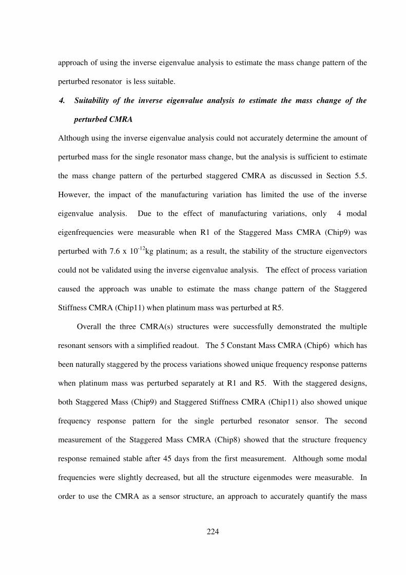
224
approach of using the inverse eigenvalue analysis to estimate the mass change pattern of the
perturbed resonator is less suitable.
4. Suitability of the inverse eigenvalue analysis to estimate the mass change of the
perturbed CMRA
Although using the inverse eigenvalue analysis could not accurately determine the amount of
perturbed mass for the single resonator mass change, but the analysis is sufficient to estimate
the mass change pattern of the perturbed staggered CMRA as discussed in Section 5.5.
However, the impact of the manufacturing variation has limited the use of the inverse
eigenvalue analysis. Due to the effect of manufacturing variations, only 4 modal
eigenfrequencies were measurable when R1 of the Staggered Mass CMRA (Chip9) was
perturbed with 7.6 x 10⁻¹²
kg platinum; as a result, the stability of the structure eigenvectors
could not be validated using the inverse eigenvalue analysis. The effect of process variation
caused the approach was unable to estimate the mass change pattern of the Staggered
Stiffness CMRA (Chip11) when platinum mass was perturbed at R5.
Overall the three CMRA(s) structures were successfully demonstrated the multiple
resonant sensors with a simplified readout. The 5 Constant Mass CMRA (Chip6) which has
been naturally staggered by the process variations showed unique frequency response patterns
when platinum mass was perturbed separately at R1 and R5. With the staggered designs,
both Staggered Mass (Chip9) and Staggered Stiffness CMRA (Chip11) also showed unique
frequency response pattern for the single perturbed resonator sensor. The second
measurement of the Staggered Mass CMRA (Chip8) showed that the structure frequency
response remained stable after 45 days from the first measurement. Although some modal
frequencies were slightly decreased, but all the structure eigenmodes were measurable. In
order to use the CMRA as a sensor structure, an approach to accurately quantify the mass

225
change pattern of the perturbed coupled resonator is required; since the mass of the
fabricated structure was changed due to the process variation, the CMRA sensor structure
requires a calibration before any mass is perturbed on the structure.
In conclusion the CMRA structure development is successful. The CMRA sensor
structure showed potential to present large resonant sensors array for the artificial nose. By
only monitoring the frequency response of the coupled resonators, the complexity of the
readout and signal processing system of large sensing system will be simplified. Using the
CMRA, requirement to integrate different sensors response is eliminated; hence, simplifying
the mathematical modelling to characterize different sensor responses.
8.2 Future Recommendations
In order to use the CMRA sensor structure in the artificial nose there are still many further
studies required:
1. An approach to estimate the mass change of the perturbed CMRA resonator
The impact of the process variation which changed some structure eigenvectors and reduced
the measurability of the eigenmodes, cause the approach of the inverse eigenvalue analysis to
become less suitable to estimate the mass change of the CMRA sensor structure; unless the
new set of eigenvectors of the fabricated CMRA are determined. Otherwise, an alternative
technique to compare the two states of the Amplitude-Frequency curve (A-F curve) (before
and after mass was perturbed on the structure) is required to determine the change of mass of
the perturbed CMRA.
2. Redesign the CMRA to include the effect of manufacturing variation
In order to use the inverse eigenvalue analysis to estimate the mass change pattern, it is
important to redesign the CMRA so that the structure eigenvectors are insensitive to the
manufacturing variation.

226
3. Using the electrostatic or mechanical tuning to compensate the manufacturing
variability
It is interesting to research an approach of a frequency tuning using the electrostatic comb
drive [169] to alter the resonant frequencies of the CMRA structure. The mechanical
frequency tuning approach using the focused ion beam platinum deposition also may be
explored.
4. An Approach to analyse and optimize the CMRA structure design
An approach such as Genetic Algorithm may be used to further analyse the CMRA
performance or optimize the CMRA structure design. The approach may be used to estimate
the amount of change of mass or stiffness of the coupled structure which affected by the
process variation. Knowing the change value will determine the new set of eigenvectors of the
fabricated CMRA. The technique may also be used to explore other alternatives to break the
CMRA structure symmetry such as staggering the coupling spring, and optimizing the
performance of the CMRA (e.g. optimizing the design parameter to improve the Q-factor of
the sensor structure).
5. Alternative method to drive and readout the CMRA sensor structure
The electrostatic drive and capacitive readout constrains the size of the CMRA structure.
Small CMRA structure is hard to be realised in order to ensure enough capacitance for the
drive and readout measurement. Large mass of the CMRA sensor reduces the sensitiveness
of the sensor to detect a small amount of perturbed mass. Other approach of drive and
readout such as a piezoelectric excitation and an optical detection may be explored, so that
the CMRA sensor can be operated in higher scale of resonant frequency (Mega hertz or
gigahertz).

227
6. Mass loading frequency effect based on real test of odour absorption – desorption
Even though many researches are important before the CMRA can be properly established for
the artificial nose, it is interesting to experiment the effect of the odour absorption -
desorption process on the sensitivity and stability of the Amplitude-Frequency curve (A-F
curve) of the CMRA structure. Then the structure can be further improved to be sensitive
within the threshold of the species of odour to be measured.
A likely sequence of operations of the final device are:
A chemically sensing membrane material which will react with the odorant molecules will be
coated on the surface of the resonator. A calibration step is required to observe the effect of
the coated material on the shift of the resonant frequency curve (note: the device will be
operated in a vacuum test chamber). An odour or a sample gas to be tested will be introduced
and directed to the coated sensing membrane material by using a flow control valve unit. The
sensor is then allowed to vibrate in few minutes before the final frequency response curve is
measured.

APPENDIX A
A-1
Consideration - Finite Element Analysis (COMSOL Multiphysics)
1. Modeling using graphical user interface (GUI, predefined physics modes or PDEs)
2. Stability of mesh: minimum element quality (3D structure: at least 0.1; and 2D: at least
0.3 [169] )
3. The effect of mesh quality on the simulation result.
Table A-1 Example of fundamental frequency of fixed-fixed beam resonator compared to
minimum element quality of mesh and time to run the simulation
Mesh Statistics
Parameter/
Others
(1) (2) (3) (4) (5) (6) (7)
DOF 17228 9622 7362 6302 6306 5022 3642 Number of
mesh points 2277 1312 1022 884 884 718 538
Number
of elements 4061 2188 1638 1384 1386 1076 746
Number of
boundary
element
493 436 406 384 382 360 330
Number of
vertex elements 24 24 24 24 24 24 24
Element
area ratio 0.0028 9.29e-4 2.5e-4 3.09e-4 1.86e-4 9.66e-5 9.51e-5
Minimum
element quality 0.6047 0.7054 0.7058 0.7059 0.6985 0.6435 0.6328
Resonator
frequency [Hz] 48761.71 48765.35 48763.09 48760.54 48759.97 48760.36 48766.58
Predefined
mesh size
Extremely
fine
Extra fine
Finer
Fine
Normal
Coarse
Extra
Coarser
Solution Time
[s] 1.438 0.766 0.547 0.438 0.453 0.344 0.235
Geometrical
Structure Design
Mode of Application/
Module
Subdomain/ Boundary/
Point setting: material,
loads, constraints, sources
Geometry Meshing:
Quality of mesh
Solving the problem:
Solver Selection
Postprocessing

APPENDIX A
A-2
48758
48760
48762
48764
48766
48768
0.5 0.55 0.6 0.65 0.7 0.75
Res
on
ant
Fre
qu
ency
[H
z]
Minimum Element Quality of mesh
Resonant Frequency of Fixed-Fixed Beam vs Minimum Element
Quality (Mesh)
Figure A.1 Simulated Frequency response of fixed-fixed beam using COMSOL Multiphysics
at different quality of mesh.

APPENDIX B
B-1
MATLAB CODES – Eigenvalue and Eigenvectors Analysis
clc clf
% insert the stiffness of R1 (resonator1), R2, R3 R4 and R5 k1=stiffnessR1; k2=stiffnessR2; k3=stiffnessR3; k4=stiffnessR4; k5=stiffnessR5;
% insert the four coupling stiffness of kc1, kc2, kc3, and kc4 kc1=coupling_stiffness_kc1; kc2=coupling_stiffness_kc2; kc3=coupling_stiffness_kc3; kc4=coupling_stiffness_kc4;
% insert the mass of R1 , R2, R3 R4 and R5 m1=massR1; m2=massR2; m3=massR3; m4=massR4; m5=massR5;
% Initial mass matrix of the 5 resonators (unperturbed Resonators) M=[m1,0,0,0,0;0,m2,0,0,0;0,0,m3,0,0;0,0,0,m4,0;0,0,0,0,m5] ;
% Stiffness matrix (resonator stiffness & coupling constant) K=[(k1+kc1), -kc1,0,0,0;-kc1, (k2+kc1+kc2),-kc2,0,0;0,-kc2,(k3+kc2+kc3),-
kc3,0;0,0,-kc3,(k4+kc3+kc4),-kc4;0,0,0,-kc4,(k5+kc4)];
Force=[0; 0; 1e-6; 0;0];
% The natural frequency of the uncoupled single degree of freedom system % (R1, R2, R3, R4, & R5) f1=(1/(2*pi))*(k1/m1)^0.5; % Natural frequency of R1 f2=(1/(2*pi))*(k2/m2)^0.5; % Natural frequency of R2 f3=(1/(2*pi))*(k3/m3)^0.5; % Natural frequency of R3 f4=(1/(2*pi))*(k4/m4)^0.5; % Natural frequency of R4 f5=(1/(2*pi))*(k5/m5)^0.5; % Natural frequency of R5
%**************************************************************************
************************************** % EIGENVALUE AND EIGENVECTORS ANALYSIS
E=(M^-1)*K;
% The column eigenvector matrix,v and diagonal eigenvalue matrix, d of the
unperturbed five degree of freedom system are: [V,d]=eig(E);
% five unsorted modal eigenfrequencies of 5 coupled resonators:- fc1=(1/(2*pi))*d(1,1)^0.5; fc2=(1/(2*pi))*d(2,2)^0.5; fc3=(1/(2*pi))*d(3,3)^0.5;

APPENDIX B
B-2
fc4=(1/(2*pi))*d(4,4)^0.5; fc5=(1/(2*pi))*d(5,5)^0.5; % the sorted 5 modal eigenfrequencies (the lowest: mode1;..; the highest:%
mode 5) yR = [fc1; fc2; fc3; fc4; fc5]; [sortyR, OrderR]=sort (yR);
% x=[1,2,3,4,5]
% The eigenvectors of the 5 coupled resonators (note: the eigenvectors for- % mode1, mode2, mode3, mode4 and mode5 were determined based on the sorted- % order of the 5 modal eigenfrequencies;
% If the sorted order is 1,2,3,4, and 5; then the eigenvectors are:- mode1=V(:,1); mode2=V(:,2); mode3=V(:,3); mode4=V(:,4); mode5=V(:,5);
%************************************************************************** % PLOTTING THE EIGENMODES
% figure(1) % Eigenmodes of 5 coupled resonators
plot(x,mode1,x,mode2,x,mode3,x,mode4,x,mode5),title('Eigenmodes of
Unperturbed 5 CMRA'), xlabel('Resonator 1 to 5'),ylabel('Eigenvectors'),
legend('mode1','mode2','mode3','mode4','mode5'), style=-1

APPENDIX C
C-1
Eigenvectors Stability: Alternative 1 (Chapter 4)
1 2 3 4 5
0.3
0.4
0.5
0.6
Stability of Eigenvectors(mode1)-Alternative 1
Resonator 1 to 5
Eig
envect
ors
Initial
+m@R1
+m@R2
+m@R3
+m@R4
+m@R5
1 2 3 4 5-1
-0.5
0
0.5
1Stability of Eigenvectors(mode3)- Alternative1
Resonator 1 to 5
Eig
env
ecto
rs
Initial
+m@R1
+m@R2
+m@R3
+m@R4
+m@R5
1 2 3 4 5
-1
-0.5
0
0.5
1Stability of Eigenvectors(mode4)- Alternative1
Resonator 1 to 5
Eig
env
ecto
rs
Initial
+m@R1
+m@R2
+m@R3
+m@R4
+m@R5
1 2 3 4 5-1
-0.5
0
0.5
1Stability of Eigenvectors (mode5)- Alternative1
Resonator 1 to 5
Eig
env
ecto
rs
Initial
+m@R1
+m@R2
+m@R3
+m@R4
+m@R5
1 2 3 4 5-0.8
-0.6
-0.4
-0.2
0
0.2
0.4
0.6
Stability of Eigenvectors(mode2)-Alternative1
Resonator 1 to 5E
igen
vec
tors
Initial
+m@R1
+m@R2
+m@R3
+m@R4
+m@R5

APPENDIX C
C-2
Eigenvectors Stability: Alternative 2
1 2 3 4 50
0.2
0.4
0.6
0.8
1Stability of Eigenvectors(mode1)-Alternative2
Resonator 1 to 5
Eig
env
ecto
rs
Initial
+m@R1
+m@R2
+m@R3
+m@R4
+m@R5
1 2 3 4 5-1
-0.5
0
0.5
1Stability of Eigenvectors(mode3)- Alternative2
Resonator 1 to 5
Eig
env
ecto
rs
Initial
+m@R1
+m@R2
+m@R3
+m@R4
+m@R5
1 2 3 4 5-1
-0.5
0
0.5
1Stability of Eigenvectors(mode4)- Alternative2
Resonator 1 to 5
Eig
env
ect
ors
Initial
+m@R1
+m@R2
+m@R3
+m@R4
+m@R5
1 2 3 4 5-1
-0.5
0
0.5
1Stability of Eigenvectors(mode5)- Alternative2
Resonator 1 to 5
Eig
en
vec
tors
Initial
+m@R1
+m@R2
+m@R3
+m@R4
+m@R5
1 2 3 4 5-0.6
-0.4
-0.2
0
0.2
0.4
0.6
0.8
Stability of Eigenvectors (mode2)-Alternative2
Resonator 1 to 5
Eig
env
ecto
rs
Initial
+m@R1
+m@R2
+m@R3
+m@R4
+m@R5

APPENDIX C
C-3
Eigenvectors Stability: Alternative 3
1 2 3 4 5-0.8
-0.6
-0.4
-0.2
0
0.2
0.4
0.6
Stability of Eigenvectors(mode2)-Alternative 3
Resonator 1 to 5E
igen
vec
tors
Initial
+m@R1
+m@R2
+m@R3
+m@R4
+m@R5
1 2 3 4 5-1
-0.5
0
0.5
1Stability of Eigenvectors(mode5)- Alternative3
Resonator 1 to 5
Eig
env
ecto
rs
Initial
+m@R1
+m@R2
+m@R3
+m@R4
+m@R5
1 2 3 4 5-1
-0.5
0
0.5
1
Stability of Eigenvectors(mode4)- Alternative3
Resonator 1 to 5
Eig
env
ect
ors
Initial
+m@R1
+m@R2
+m@R3
+m@R4
+m@R5
1 2 3 4 5
-1
-0.5
0
0.5
1Stability of Eigenvectors(mode3)- Alternative3
Resonator 1 to 5
Eig
env
ecto
rs
Initial
+m@R1
+m@R2
+m@R3
+m@R4
+m@R5
1 2 3 4 5-1
-0.5
0
0.5
1Stability of Eigenvectors(mode1)- Alternative3
Resonator 1 to 5
Eig
env
ecto
rs
Initial
+m@R1
+m@R2
+m@R3
+m@R4
+m@R5

APPENDIX C
C-4
Eigenvectors Stability: Alternative 4
1 2 3 4 5-1
-0.5
0
0.5
1
Stability of Eigenvectors(mode4)- Alternative4
Resonator 1 to 5
Eig
env
ecto
rs
Initial
+m@R1
+m@R2
+m@R3
+m@R4
+m@R51 2 3 4 5
-1
-0.5
0
0.5
1Stability of Eigenvectors(mode3)- Alternative4
Resonator 1 to 5
Eig
env
ecto
rs
Initial
+m@R1
+m@R2
+m@R3
+m@R4
+m@R5
1 2 3 4 5-0.5
0
0.5
1
Stability of Eigenvectors(mode5)- Alternative4
Eig
env
ecto
rs
Initial
+m@R1
+m@R2
+m@R3
+m@R4
+m@R5
1 2 3 4 50
0.2
0.4
0.6
0.8
1Stability of Eigenvectors (mode1)-Alternative4
Resonator 1 to 5
Eig
env
ecto
rs
Initial
+m@R1
+m@R2
+m@R3
+m@R4
+m@R5
1 2 3 4 5
0
0.2
0.4
0.6
0.8
Stability of Eigenvectors(mode2)-Alternative4
Resonator 1 to 5
Eig
env
ecto
rs
Initial
+m@R1
+m@R2
+m@R3
+m@R4
+m@R5

APPENDIX C
C-5
Eigenvectors Stability: Alternative 5
1 2 3 4 5-0.8-0.6-0.4-0.2
00.20.40.60.8
1
Stability of Eigenvectors (mode2)- Alternative 5
Resonator 1 to 5
Eig
env
ecto
rs
Initial
+m@R1
+m@R2
+m@R3
+m@R4
+m@R5
1 2 3 4 5
-0.5
0.5
1
Stability of Eigenvectors (mode1)- Alternative 5
Resonator 1 to 5
Eig
env
ecto
rs
Initial
+m@R1
+m@R2
+m@R3
+m@R4
+m@R5
1 2 3 4 5
-0.5
0
0.5
Stability of Eigenvectors (mode3)-
Alternative 5
Resonator 1 to 5
Eig
env
ecto
rs
Initial
+m@R1
+m@R2
+m@R3
+m@R4
+m@R5
1 2 3 4 5
-0.8
-0.4
0
0.4
0.81
Stability of Eigenvectors (mode4)-
Alternative 5
Resonator 1 to 5
Eig
env
ecto
rs
Initial
+m@R1
+m@R2
+m@R3
+m@R4
+m@R5
1 2 3 4 5-0.5
0
0.5
1
Stability of Eigenvectors (mode5)-
Alternative 5
Resonator 1 to 5
Eig
env
ecto
rs
Initial
+m@R1
+m@R2
+m@R3
+m@R4
+m@R5

APPENDIX C
C-6
Eigenvectors Stability: Alternative 6
1 2 3 4 5-1
0
1
Stability of Eigenvectors(mode2)-
Alternative6
Resonator 1 to 5
Eig
env
ecto
rs
Initial
+m@R1
+m@R2
+m@R3
+m@R4
+m@R5
1 2 3 4 5
-0.8
-0.4
0
0.4
Stability of Eigenvectors (mode1)-
Alternative 6
Resonator 1 to 5
RE
igen
vec
tors
Initial
+m@R1
+m@R2
+m@R3
+m@R4
+m@R5
1 2 3 4 5
-0.8
-0.4
0
0.4
0.8
Stability of Eigenvectors (mode3)-
Alternative 6
Resonator 1 to 5
Eig
envec
tors
Initial
+m@R1
+m@R2
+m@R3
+m@R4
+m@R5
1 2 3 4 5
-0.4
0
0.4
Stability of Eigenvectors (mode4)-
Alternative 6
Resonator 1 to 5
Eig
env
ecto
rs
Initial
+m@R1
+m@R2
+m@R3
+m@R4
+m@R5
1 2 3 4 5
-0.4
0
0.4
0.8
Stability of Eigenvectors (mode5)-
Alternative 6
Resonator 1 to 5
Eig
env
ecto
rs
Initial
+m@R1
+m@R2
+m@R3
+m@R4
+m@R5

APPENDIX D
D-1
Eigenvectors of 5 Staggered Mass CMRA (Unperturbed (Initial) and Perturbed):
Analysed using Lumped Mass Analysis (Chapter 5)
Note:
1. **IEA: Determination of mass change pattern of the resonator using Inverse
Eigenvalue Analysis, Y-Successful; N-Failed
2. (*) Original ranked perturbed eigenvectors;
(***) perturbed eigenvectors (ranked based on the unperturbed eigenvectors)
3. Highlighted eigenvectors:-
Incomparable perturbed eigenvectors;
Symmetrical perturbed eigenvectors
Table D-1 Perturbed mass: 3.0615 x 10⁻¹¹
kg
Eigenvector/ Analysis
Perturbed Mass [kg]
mode1 mode2 mode3 mode4 mode5
Initial
-0.1797
-0.5010
-0.7398
-0.3734
-0.1731
-0.3397
-0.5276
0.0438
0.5230
0.5751
0.4649
0.3787
-0.5412
0.0948
0.5818
-0.6413
0.3523
0.0744
-0.5231
0.4305
-0.4920
0.4400
-0.3727
0.5495
-0.3514
(*)(***)
(+) 3.0615 x 10⁻¹¹
at
R1
(**IEA:Y)
-0.2535
-0.5190
-0.7174
-0.3544
-0.1617
-0.5280
-0.4810
0.1869
0.4894
0.4641
0.5051
0.1081
-0.5054
0.2326
0.6508
-0.6132
0.6194
-0.1634
-0.3029
0.3492
-0.1908
0.3101
-0.3928
0.7001
-0.4722
(*)
(+) 3.0615 x 10⁻¹¹
at
R2
(**IEA:N)
-0.2162
-0.6572
-0.6527
-0.2853
-0.1183
-0.2943
-0.5219
0.2929
0.5584
0.4934
0.3204
0.2888
-0.5820
0.1676
0.6687
0.8202
-0.3626
0.0158
0.3281
-0.2965
0.3247
-0.2595
0.3701
-0.6866
0.4678
(***)
0.8202
-0.3626
0.0158
0.3281
-0.2965
-0.2943
-0.5219
0.2929
0.5584
0.4934
0.3204
0.2888
-0.5820
0.1676
0.6687
0.3247
-0.2595
0.3701
-0.6866
0.4678
-0.2162
-0.6572
-0.6527
-0.2853
-0.1183
(*)
(+) 3.0615 x 10⁻¹¹
at
R3 (**IEA:N)
0.1274
0.4142
0.8304
0.3274
0.1247
-0.3530
-0.5489
0.0443
0.5094
0.5592
0.4517
0.4551
-0.4527
0.2088
0.5834
0.5995
-0.3266
-0.0754
0.5603
-0.4629
-0.5596
0.4522
-0.2888
0.5229
-0.3542
(***)
0.5995
-0.3266
-0.0754
0.5603
-0.4629
-0.3530
-0.5489
0.0443
0.5094
0.5592
0.4517
0.4551
-0.4527
0.2088
0.5834
-0.5596
0.4522
-0.2888
0.5229
-0.3542
0.1274
0.4142
0.8304
0.3274
0.1247

APPENDIX D
D-2
(*)
(+) 3.0615 x 10⁻¹¹
at
R4
(**IEA:N)
0.1456
0.4268
0.7011
0.5067
0.2201
-0.3224
-0.5746
-0.1358
0.5564
0.4877
-0.4851
-0.3983
0.5627
-0.0900
-0.5303
-0.3857
0.1040
0.2484
-0.6018
0.6454
0.7139
-0.5562
0.3129
-0.2371
0.1639
(***) -0.4851
-0.3983
0.5627
-0.0900
-0.5303
-0.3857
0.1040
0.2484
-0.6018
0.6454
0.7139
-0.5562
0.3129
-0.2371
0.1639
-0.3224
-0.5746
-0.1358
0.5564
0.4877
0.1456
0.4268
0.7011
0.5067
0.2201
(*)
(+) 3.0615 x 10⁻¹¹
at
R5
(**IEA:Y)
-0.1664
-0.4700
-0.7142
-0.4016
-0.2829
-0.2234
-0.4285
-0.1781
0.3795
0.7686
-0.5162
-0.5215
0.5160
0.1754
-0.4058
0.5517
-0.2322
-0.2089
0.6838
-0.3613
0.6096
-0.5118
0.3671
-0.4420
0.1906
(***) -0.5162
-0.5215
0.5160
0.1754
-0.4058
-0.2234
-0.4285
-0.1781
0.3795
0.7686
-0.1664
-0.4700
-0.7142
-0.4016
-0.2829
0.5517
-0.2322
-0.2089
0.6838
-0.3613
0.6096
-0.5118
0.3671
-0.4420
0.1906
Table D-2 Perturbed mass: 1 x 10-11
kg
Eigenvector/ Analysis
Perturbed Mass [kg]
mode1 mode2 mode3 mode4 mode5
Initial
-0.1797
-0.5010
-0.7398
-0.3734
-0.1731
-0.3397
-0.5276
0.0438
0.5230
0.5751
0.4649
0.3787
-0.5412
0.0948
0.5818
-0.6413
0.3523
0.0744
-0.5231
0.4305
-0.4920
0.4400
-0.3727
0.5495
-0.3514
(*)(***)
(+) 1 x 10-11
at
R1
(**IEA: Y)
-0.1990
-0.5061
-0.7345
-0.3686
-0.1702
-0.3927
-0.5222
0.0816
0.5165
0.5474
0.4929
0.3025
-0.5356
0.1334
0.6007
-0.6781
0.4729
-0.0264
-0.4155
0.3783
-0.3434
0.3827
-0.3911
0.6375
-0.4198
(*)(***)
(+) 1 x 10-11
at
R2
(**IEA: Y)
-0.1929
-0.5509
-0.7172
-0.3473
-0.1561
-0.3316
-0.5390
0.1278
0.5351
0.5449
0.4115
0.3490
-0.5603
0.1214
0.6165
-0.7141
0.3680
0.0378
-0.4535
0.3841
-0.4357
0.3711
-0.3754
0.6091
-0.4006
(*)
(+) 1 x 10-11
at
R3
(**IEA: N)
-0.1612
-0.4720
-0.7732
-0.3591
-0.1562
-0.3440
-0.5346
0.0440
0.5187
0.5700
0.4611
0.4082
-0.5135
0.1364
0.5818
0.6280
-0.3441
-0.0748
0.5356
-0.4413
0.5158
-0.4442
0.3419
-0.5424
0.3545

APPENDIX D
D-3
(***) 0.6280
-0.3441
-0.0748
0.5356
-0.4413
-0.3440
-0.5346
0.0440
0.5187
0.5700
0.4611
0.4082
-0.5135
0.1364
0.5818
0.5158
-0.4442
0.3419
-0.5424
0.3545
-0.1612
-0.4720
-0.7732
-0.3591
-0.1562
(*)
(+) 1 x 10-11
at
R4
(**IEA: N)
0.1702
0.4810
0.7313
0.4120
0.1877
-0.3328
-0.5408
-0.0104
0.5411
0.5512
-0.4719
-0.3854
0.5487
-0.0933
-0.5647
-0.5366
0.2506
0.1548
-0.5926
0.5236
-0.6068
0.5058
-0.3556
0.4159
-0.2768
(***) -0.5366
0.2506
0.1548
-0.5926
0.5236
-0.3328
-0.5408
-0.0104
0.5411
0.5512
-0.4719
-0.3854
0.5487
-0.0933
-0.5647
-0.6068
0.5058
-0.3556
0.4159
-0.2768
0.1702
0.4810
0.7313
0.4120
0.1877
(*)
(+) 1 x 10-11
at
R5
(**IEA: Y)
0.1768
0.4943
0.7348
0.3806
0.1990
-0.2975
-0.4907
-0.0262
0.4908
0.6551
-0.4862
-0.4347
0.5382
0.0086
-0.5338
0.6030
-0.3029
-0.1302
0.5955
-0.4160
0.5466
-0.4747
0.3736
-0.5072
0.2814
(***) 0.1768
0.4943
0.7348
0.3806
0.1990
-0.2975
-0.4907
-0.0262
0.4908
0.6551
-0.4862
-0.4347
0.5382
0.0086
-0.5338
0.6030
-0.3029
-0.1302
0.5955
-0.4160
0.5466
-0.4747
0.3736
-0.5072
0.2814
Table D-3 Perturbed mass: 7.6 x 10⁻¹²
kg
Eigenvector/ Analysis
Perturbed Mass [kg]
mode1 mode2 mode3 mode4 mode5
Initial
-0.1797
-0.5010
-0.7398
-0.3734
-0.1731
-0.3397
-0.5276
0.0438
0.5230
0.5751
0.4649
0.3787
-0.5412
0.0948
0.5818
-0.6413
0.3523
0.0744
-0.5231
0.4305
-0.4920
0.4400
-0.3727
0.5495
-0.3514
(*)(***)
(+) 7.6 x 10⁻¹²
at
R1
(**IEA: Y)
-0.1940
-0.5048
-0.7359
-0.3699
-0.1709
-0.3790
-0.5241
0.0717
0.5184
0.5548
0.4871
0.3220
-0.5374
0.1235
0.5958
-0.6760
0.4481
-0.0047
-0.4376
0.3882
-0.3735
0.3955
-0.3888
0.6220
-0.4074
(*)(***)
(+) 7.6 x 10⁻¹²
at
R2
(**IEA: Y)
-0.1898
-0.5387
-0.7231
-0.3539
-0.1603
-0.3343
-0.5374
0.1076
0.5323
0.5519
0.4238
0.3563
-0.5563
0.1152
0.6088
-0.6979
0.3655
0.0461
-0.4701
0.3953
-0.4497
0.3870
-0.3752
0.5961
-0.3897
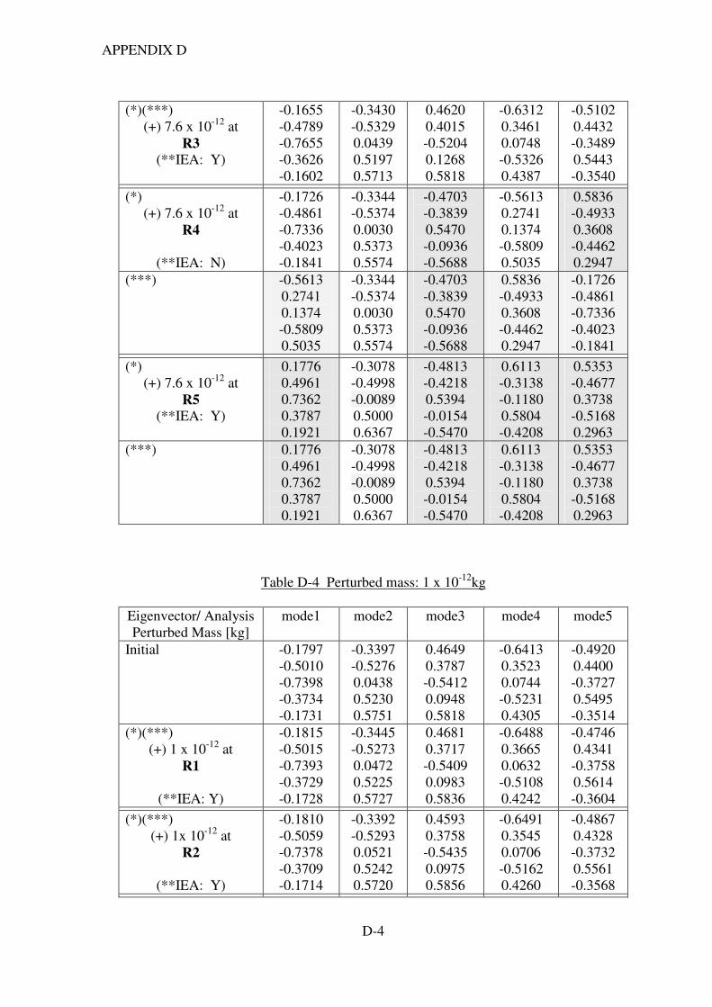
APPENDIX D
D-4
(*)(***)
(+) 7.6 x 10⁻¹²
at
R3
(**IEA: Y)
-0.1655
-0.4789
-0.7655
-0.3626
-0.1602
-0.3430
-0.5329
0.0439
0.5197
0.5713
0.4620
0.4015
-0.5204
0.1268
0.5818
-0.6312
0.3461
0.0748
-0.5326
0.4387
-0.5102
0.4432
-0.3489
0.5443
-0.3540
(*)
(+) 7.6 x 10⁻¹²
at
R4
(**IEA: N)
-0.1726
-0.4861
-0.7336
-0.4023
-0.1841
-0.3344
-0.5374
0.0030
0.5373
0.5574
-0.4703
-0.3839
0.5470
-0.0936
-0.5688
-0.5613
0.2741
0.1374
-0.5809
0.5035
0.5836
-0.4933
0.3608
-0.4462
0.2947
(***) -0.5613
0.2741
0.1374
-0.5809
0.5035
-0.3344
-0.5374
0.0030
0.5373
0.5574
-0.4703
-0.3839
0.5470
-0.0936
-0.5688
0.5836
-0.4933
0.3608
-0.4462
0.2947
-0.1726
-0.4861
-0.7336
-0.4023
-0.1841
(*)
(+) 7.6 x 10⁻¹²
at
R5
(**IEA: Y)
0.1776
0.4961
0.7362
0.3787
0.1921
-0.3078
-0.4998
-0.0089
0.5000
0.6367
-0.4813
-0.4218
0.5394
-0.0154
-0.5470
0.6113
-0.3138
-0.1180
0.5804
-0.4208
0.5353
-0.4677
0.3738
-0.5168
0.2963
(***)
0.1776
0.4961
0.7362
0.3787
0.1921
-0.3078
-0.4998
-0.0089
0.5000
0.6367
-0.4813
-0.4218
0.5394
-0.0154
-0.5470
0.6113
-0.3138
-0.1180
0.5804
-0.4208
0.5353
-0.4677
0.3738
-0.5168
0.2963
Table D-4 Perturbed mass: 1 x 10-12
kg
Eigenvector/ Analysis
Perturbed Mass [kg]
mode1 mode2 mode3 mode4 mode5
Initial
-0.1797
-0.5010
-0.7398
-0.3734
-0.1731
-0.3397
-0.5276
0.0438
0.5230
0.5751
0.4649
0.3787
-0.5412
0.0948
0.5818
-0.6413
0.3523
0.0744
-0.5231
0.4305
-0.4920
0.4400
-0.3727
0.5495
-0.3514
(*)(***)
(+) 1 x 10-12
at
R1
(**IEA: Y)
-0.1815
-0.5015
-0.7393
-0.3729
-0.1728
-0.3445
-0.5273
0.0472
0.5225
0.5727
0.4681
0.3717
-0.5409
0.0983
0.5836
-0.6488
0.3665
0.0632
-0.5108
0.4242
-0.4746
0.4341
-0.3758
0.5614
-0.3604
(*)(***)
(+) 1x 10-12
at
R2
(**IEA: Y)
-0.1810
-0.5059
-0.7378
-0.3709
-0.1714
-0.3392
-0.5293
0.0521
0.5242
0.5720
0.4593
0.3758
-0.5435
0.0975
0.5856
-0.6491
0.3545
0.0706
-0.5162
0.4260
-0.4867
0.4328
-0.3732
0.5561
-0.3568

APPENDIX D
D-5
(+) 1x 10-12
at
R3
(**IEA: Y)
-0.1778
-0.4981
-0.7433
-0.3720
-0.1714
-0.3401
-0.5283
0.0438
0.5226
0.5746
0.4645
0.3818
-0.5386
0.0991
0.5818
-0.6400
0.3515
0.0745
-0.5244
0.4316
-0.4945
0.4404
-0.3694
0.5489
-0.3518
(*)(***)
(+) 1x 10-12
at
R4
(**IEA: Y)
-0.1788
-0.4992
-0.7391
-0.3770
-0.1745
-0.3389
-0.5288
0.0386
0.5251
0.5730
0.4656
0.3794
-0.5420
0.0946
0.5801
-0.6311
0.3421
0.0832
-0.5324
0.4408
-0.5054
0.4481
-0.3717
0.5358
-0.3443
(*)
(+) 1x 10-12
at
R5
(**IEA: N)
0.1794
0.5004
0.7394
0.3740
0.1754
-0.3356
-0.5241
0.0371
0.5205
0.5834
-0.4671
-0.3844
0.5412
-0.0841
-0.5780
-0.6371
0.3469
0.0806
-0.5315
0.4298
-0.4984
0.4442
-0.3730
0.5451
-0.3435
(***) -0.6371
0.3469
0.0806
-0.5315
0.4298
-0.3356
-0.5241
0.0371
0.5205
0.5834
-0.4671
-0.3844
0.5412
-0.0841
-0.5780
-0.4984
0.4442
-0.3730
0.5451
-0.3435
0.1794
0.5004
0.7394
0.3740
0.1754
Table D-5 Perturbed mass: 1 x 10-13
kg
Eigenvector/ Analysis
Perturbed Mass [kg]
mode1 mode2 mode3 mode4 mode5
Initial
-0.1797
-0.5010
-0.7398
-0.3734
-0.1731
-0.3397
-0.5276
0.0438
0.5230
0.5751
0.4649
0.3787
-0.5412
0.0948
0.5818
-0.6413
0.3523
0.0744
-0.5231
0.4305
-0.4920
0.4400
-0.3727
0.5495
-0.3514
(*)(***)
(+) 1 x 10-13
at
R1
(**IEA: Y)
-0.1799
-0.5011
-0.7398
-0.3733
-0.1731
-0.3402
-0.5276
0.0441
0.5230
0.5749
0.4652
0.3780
-0.5412
0.0951
0.5820
-0.6421
0.3538
0.0733
-0.5219
0.4299
-0.4902
0.4394
-0.3730
0.5507
-0.3523
(*)(***)
(+) 1x 10-13
at
R2
(**IEA: Y)
-0.1798
-0.5015
-0.7396
-0.3731
-0.1729
-0.3396
-0.5278
0.0446
0.5231
0.5748
0.4644
0.3784
-0.5415
0.0951
0.5822
-0.6421
0.3525
0.0740
-0.5225
0.4301
-0.4915
0.4393
-0.3727
0.5502
-0.3520
(*)(***)
(+) 1x 10-13
at
R3
(**IEA: Y)
-0.1795
-0.5007
-0.7402
-0.3732
-0.1729
-0.3397
-0.5277
0.0438
0.5230
0.5751
0.4649
0.3790
-0.5410
0.0952
0.5818
-0.6412
0.3522
0.0744
-0.5233
0.4306
-0.4922
0.4400
-0.3723
0.5495
-0.3515

APPENDIX D
D-6
(*)(***)
(+) 1x 10-13
at
R4
(**IEA: Y)
-0.1796
-0.5008
-0.7398
-0.3737
-0.1732
-0.3396
-0.5277
0.0432
0.5232
0.5749
0.4650
0.3787
-0.5413
0.0948
0.5817
-0.6403
0.3513
0.0753
-0.5241
0.4316
-0.4934
0.4408
-0.3726
0.5481
-0.3507
(*)(***)
(+) 1x 10-13
at
R5
(**IEA: Y)
-0.1797
-0.5010
-0.7398
-0.3734
-0.1733
-0.3393
-0.5273
0.0431
0.5228
0.5760
0.4651
0.3792
-0.5412
0.0937
0.5815
-0.6409
0.3518
0.0750
-0.5240
0.4305
-0.4927
0.4404
-0.3727
0.5491
-0.3506

APPENDIX E
E-1
Eigenvectors of 5 Staggered Stiffness CMRA (Unperturbed (Initial) and Perturbed):
Analysed using Lumped Mass Analysis (Chapter 5)
Note:
1. **IEA: Determination of mass change pattern of the resonator using Inverse
Eigenvalue Analysis, Y-Successful; N-Failed
2. (*) Original ranked perturbed eigenvectors;
(***) perturbed eigenvectors (ranked based on the unperturbed eigenvectors)
3. Highlighted eigenvectors:-
Incomparable perturbed eigenvectors;
Symmetrical perturbed eigenvectors
Table E-1 Perturbed mass: 3.0615 x 10⁻¹¹
kg
Eigenvector/ Analysis
Perturbed Mass [kg]
mode1 mode2 mode3 mode4 mode5
Initial
-0.2153
-0.3851
-0.6638
-0.5621
-0.2207
0.6307
0.5064
0.0261
-0.4948
-0.3167
0.5632
-0.0537
-0.5846
0.3218
0.4843
-0.3659
0.4931
-0.0552
-0.3987
0.6789
0.3240
-0.5910
0.4619
-0.4199
0.3950
(*) (***)
(+) 3.0615 x 10⁻¹¹
at
R1
(**IEA:Y)
0.4112
0.4342
0.6119
0.4837
0.1846
-0.7391
-0.2928
0.2406
0.4964
0.2523
0.3928
-0.2857
-0.5614
0.4356
0.5091
-0.2877
0.6027
-0.1728
-0.3224
0.6483
0.2036
-0.5312
0.4730
-0.4773
0.4741
(*)
(+) 3.0615 x 10⁻¹¹
at
R2
(**IEA:Y)
-0.2788
-0.5470
-0.6247
-0.4529
-0.1664
0.4975
0.5064
-0.1440
-0.6008
-0.3381
0.5926
-0.0551
-0.5692
0.3147
0.4719
0.5407
-0.5853
0.2926
0.1620
-0.5031
0.1825
-0.3027
0.4249
-0.5569
0.6200
(***)
-0.2788
-0.5470
-0.6247
-0.4529
-0.1664
0.4975
0.5064
-0.1440
-0.6008
-0.3381
0.5926
-0.0551
-0.5692
0.3147
0.4719
0.1825
-0.3027
0.4249
-0.5569
0.6200
0.5407
-0.5853
0.2926
0.1620
-0.5031
(*) (***)
(+) 3.0615 x 10⁻¹¹
at
R3
(**IEA:Y)
-0.1567
-0.3464
-0.7804
-0.4705
-0.1584
0.6209
0.4989
0.0265
-0.5088
-0.3256
0.5620
0.0860
-0.5064
0.4371
0.4788
-0.3902
0.5249
-0.0566
-0.3807
0.6512
0.3508
-0.5911
0.3535
-0.4308
0.4659
(*) (***)
(+) 3.0615 x 10⁻¹¹
at
R4
(**IEA:N)
-0.1223
-0.2606
-0.5617
-0.7330
-0.2537
0.5957
0.5832
0.2635
-0.4207
-0.2420
0.6300
-0.0156
-0.6373
0.2627
0.3574
-0.2681
0.3265
0.0318
-0.3767
0.8238
-0.4035
0.6976
-0.4580
0.2610
-0.2696
APPENDIX E
E-2
(*) (***)
(+) 3.0615 x 10⁻¹¹
at
R5
(**IEA:Y)
-0.1892
-0.3494
-0.6287
-0.5843
-0.3247
0.5543
0.5150
0.1786
-0.4137
-0.4738
-0.6108
-0.0842
0.5576
-0.0413
-0.5543
-0.3665
0.3678
0.1790
-0.6126
0.5684
0.3900
-0.6869
0.4806
-0.3348
0.1817
Table E-2 Perturbed mass: 1 x 10-11
kg
Eigenvector/ Analysis
Perturbed Mass [kg]
mode1 mode2 mode3 mode4 mode5
Initial
-0.2153
-0.3851
-0.6638
-0.5621
-0.2207
0.6307
0.5064
0.0261
-0.4948
-0.3167
0.5632
-0.0537
-0.5846
0.3218
0.4843
-0.3659
0.4931
-0.0552
-0.3987
0.6789
0.3240
-0.5910
0.4619
-0.4199
0.3950
(*) (***)
(+) 1 x 10-11
at
R1
(**IEA:Y)
-0.2583
-0.3978
-0.6556
-0.5473
-0.2136
0.6919
0.4522
-0.0524
-0.4814
-0.2867
0.5110
-0.1465
-0.5808
0.3675
0.4950
-0.3408
0.5408
-0.1025
-0.3688
0.6670
0.2743
-0.5691
0.4686
-0.4448
0.4283
(*) (***)
(+) 1 x 10-11
at
R2
(**IEA:Y)
-0.2360
-0.4324
-0.6564
-0.5330
-0.2057
0.5913
0.5161
-0.0234
-0.5280
-0.3235
0.5727
-0.0542
-0.5798
0.3196
0.4804
-0.4370
0.5557
-0.1472
-0.3149
0.6159
0.2764
-0.4821
0.4591
-0.4860
0.4941
(*) (***)
(+) 1 x 10-11
at
R3
(**IEA:Y)
-0.1959
-0.3744
-0.7051
-0.5332
-0.1997
0.6275
0.5040
0.0263
-0.4994
-0.3196
0.5623
-0.0036
-0.5640
0.3639
0.4830
-0.3738
0.5035
-0.0557
-0.3930
0.6702
0.3355
-0.5939
0.4224
-0.4240
0.4201
(*) (***)
(+) 1 x 10-11
at
R4
(**IEA:Y)
-0.1836
-0.3452
-0.6365
-0.6217
-0.2355
0.6186
0.5360
0.1108
-0.4802
-0.2953
0.5890
-0.0407
-0.6063
0.3028
0.4383
-0.3310
0.4315
-0.0186
-0.4006
0.7372
-0.3577
0.6374
-0.4636
0.3579
-0.3504
(*) (***)
(+) 1 x 10-11
at
R5
(**IEA:Y)
-0.2087
-0.3763
-0.6558
-0.5689
-0.2475
0.6122
0.5102
0.0653
-0.4795
-0.3615
0.5743
-0.0155
-0.5815
0.2423
0.5226
-0.3522
0.4304
0.0386
-0.4917
0.6689
-0.3588
0.6427
-0.4755
0.3825
-0.2929

APPENDIX E
E-3
Table E-3 Perturbed mass: 7.6 x 10⁻¹²
kg
Eigenvector/ Analysis
Perturbed Mass [kg]
mode1 mode2 mode3 mode4 mode5
Initial
-0.2153
-0.3851
-0.6638
-0.5621
-0.2207
0.6307
0.5064
0.0261
-0.4948
-0.3167
0.5632
-0.0537
-0.5846
0.3218
0.4843
-0.3659
0.4931
-0.0552
-0.3987
0.6789
0.3240
-0.5910
0.4619
-0.4199
0.3950
(*) (***)
(+) 7.6 x 10⁻¹²
at
R1
(**IEA: Y)
-0.2467
-0.3944
-0.6580
-0.5515
-0.2156
0.6788
0.4667
-0.0329
-0.4840
-0.2935
0.5245
-0.1256
-0.5822
0.3572
0.4926
-0.3470
0.5307
-0.0921
-0.3755
0.6696
0.2852
-0.5742
0.4674
-0.4395
0.4212
(*) (***)
(+) 7.6 x 10⁻¹²
at
R2
(**IEA: Y)
-0.2309
-0.4205
-0.6586
-0.5406
-0.2095
0.6012
0.5145
-0.0109
-0.5198
-0.3218
0.5704
-0.0541
-0.5809
0.3201
0.4814
-0.4209
0.5436
-0.1257
-0.3354
0.6317
0.2887
-0.5082
0.4613
-0.4720
0.4721
(*) (***)
(+) 7.6 x 10⁻¹²
at
R3
(**IEA: Y)
-0.2005
-0.3772
-0.6954
-0.5403
-0.2047
0.6283
0.5045
0.0262
-0.4983
-0.3189
0.5624
-0.0153
-0.5695
0.3542
0.4834
-0.3719
0.5010
-0.0556
-0.3944
0.6723
0.3330
-0.5935
0.4315
-0.4231
0.4143
(*) (***)
(+) 7.6 x 10⁻¹²
at
R4
(**IEA: Y)
-0.1912
-0.3551
-0.6437
-0.6075
-0.2322
0.6214
0.5292
0.0908
-0.4848
-0.3009
0.5832
-0.0438
-0.6015
0.3075
0.4490
-0.3392
0.4458
-0.0266
-0.4011
0.7243
-0.3503
0.6274
-0.4636
0.3719
-0.3610
(*) (***)
(+) 7.6 x 10⁻¹²
at
R5
(**IEA: Y)
-0.2104
-0.3786
-0.6579
-0.5672
-0.2405
0.6171
0.5094
0.0550
-0.4839
-0.3501
0.5713
-0.0253
-0.5827
0.2627
0.5143
-0.3537
0.4428
0.0181
-0.4720
0.6751
-0.3522
0.6332
-0.4735
0.3906
-0.3134
Table E-4 Perturbed mass: 1 x 10-12
kg
Eigenvector/ Analysis
Perturbed Mass [kg]
mode1 mode2 mode3 mode4 mode5
Initial
-0.2153
-0.3851
-0.6638
-0.5621
-0.2207
0.6307
0.5064
0.0261
-0.4948
-0.3167
0.5632
-0.0537
-0.5846
0.3218
0.4843
-0.3659
0.4931
-0.0552
-0.3987
0.6789
0.3240
-0.5910
0.4619
-0.4199
0.3950

APPENDIX E
E-4
(*) (***)
(+) 1 x 10-12
at
R1
(**IEA: Y)
-0.2190
-0.3862
-0.6632
-0.5609
-0.2201
0.6375
0.5017
0.0186
-0.4933
-0.3136
0.5586
-0.0636
-0.5845
0.3267
0.4854
-0.3636
0.4986
-0.0604
-0.3955
0.6776
0.3185
-0.5887
0.4628
-0.4228
0.3988
(*) (***)
(+) 1x 10-12
at
R2
(**IEA: Y)
-0.2173
-0.3895
-0.6633
-0.5595
-0.2193
0.6269
0.5077
0.0215
-0.4980
-0.3174
0.5641
-0.0538
-0.5841
0.3216
0.4840
-0.3734
0.5007
-0.0645
-0.3907
0.6731
0.3199
-0.5803
0.4624
-0.4273
0.4056
(*) (***)
(+) 1x 10-12
at
R3
(**IEA: Y)
-0.2134
-0.3841
-0.6681
-0.5593
-0.2186
0.6303
0.5061
0.0262
-0.4953
-0.3170
0.5631
-0.0485
-0.5829
0.3262
0.4842
-0.3667
0.4942
-0.0552
-0.3981
0.6781
0.3253
-0.5914
0.4578
-0.4204
0.3976
(*) (***)
(+) 1x 10-12
at
R4
(**IEA: Y)
-0.2122
-0.3812
-0.6614
-0.5681
-0.2223
0.6294
0.5095
0.0347
-0.4939
-0.3148
0.5660
-0.0524
-0.5870
0.3200
0.4796
-0.3624
0.4868
-0.0512
-0.3994
0.6853
0.3278
-0.5962
0.4623
-0.4133
0.3906
(*) (***)
(+) 1x 10-12
at
R5
(**IEA: Y)
-0.2147
-0.3843
-0.6631
-0.5628
-0.2231
0.6290
0.5068
0.0297
-0.4936
-0.3209
0.5642
-0.0502
-0.5845
0.3145
0.4885
-0.3636
0.4855
-0.0448
-0.4094
0.6801
0.3285
-0.5978
0.4641
-0.4158
0.3827
Table E-5 Perturbed mass: 1 x 10-13
kg
Eigenvector/ Analysis
Perturbed Mass [kg]
mode1 mode2 mode3 mode4 mode5
Initial
-0.2153
-0.3851
-0.6638
-0.5621
-0.2207
0.6307
0.5064
0.0261
-0.4948
-0.3167
0.5632
-0.0537
-0.5846
0.3218
0.4843
-0.3659
0.4931
-0.0552
-0.3987
0.6789
0.3240
-0.5910
0.4619
-0.4199
0.3950
(*) (***)
(+) 1 x 10-13
at
R1
(**IEA: Y)
-0.2157
-0.3852
-0.6638
-0.5620
-0.2206
0.6313
0.5059
0.0254
-0.4947
-0.3164
0.5627
-0.0547
-0.5846
0.3223
0.4844
-0.3657
0.4937
-0.0557
-0.3983
0.6788
0.3235
-0.5907
0.4620
-0.4202
0.3954
(*) (***)
(+) 1x 10-13
at
R2
(**IEA: Y)
-0.2155
-0.3855
-0.6638
-0.5619
-0.2205
0.6303
0.5065
0.0257
-0.4952
-0.3168
0.5633
-0.0537
-0.5846
0.3218
0.4843
-0.3667
0.4939
-0.0561
-0.3979
0.6784
0.3236
-0.5899
0.4620
-0.4207
0.3961

APPENDIX E
E-5
(*) (***)
(+) 1x 10-13
at
R3
(**IEA: Y)
-0.2151
-0.3850
-0.6643
-0.5619
-0.2205
0.6306
0.5063
0.0261
-0.4949
-0.3168
0.5632
-0.0532
-0.5844
0.3223
0.4843
-0.3660
0.4932
-0.0552
-0.3986
0.6788
0.3242
-0.5910
0.4615
-0.4200
0.3953
(*) (***)
(+) 1x 10-13
at
R4
(**IEA: Y)
-0.2150
-0.3847
-0.6636
-0.5627
-0.2208
0.6305
0.5067
0.0270
-0.4948
-0.3165
0.5635
-0.0536
-0.5849
0.3216
0.4839
-0.3656
0.4925
-0.0548
-0.3988
0.6796
0.3244
-0.5915
0.4620
-0.4192
0.3946
(*) (***)
(+) 1x 10-13
at
R5
(**IEA: Y)
-0.2152
-0.3850
-0.6638
-0.5622
-0.2209
0.6305
0.5064
0.0265
-0.4947
-0.3171
0.5633
-0.0534
-0.5846
0.3211
0.4848
-0.3657
0.4924
-0.0541
-0.3998
0.6791
0.3245
-0.5917
0.4622
-0.4195
0.3938

APPENDIX F
F-1
Effective Mass and Stiffness of Comb-Drive Resonator
Figure F.1 (a) Integrated comb-drive resonator; (b) An anchor spring of the resonator
By assuming beam 2 is rigid, and two beams of beam 1 and beam 3 are in series, stiffness of
an anchor spring, k [1];
31
31
kk
kkk
+= ;
( )31
11
12
L
EIk = ;
( )33
3123
L
EIk = ;
( )12
11
3bhI = ;
( )12
33
3bh
I =
Assuming width of beam 1, b1 = b3 = b; Stiffness of an anchor spring, k;
( ) ( )333
1
3
LL
Ehbk
+= (Equation F-1)
or if L1 = L3, then;
3
3
2L
Ehbk = (Equation F-2)
Mc
(a)
(b)
L1
L3
L2 M1
M2
M3
M
b1
b2
L
b
h
δ ι

APPENDIX F
F-2
Where E: Young’s Modulus; k: beam stiffness; h: thickness of device; b: width of the beam; I:
second moment of area
Effective mass of resonator,
−
++
+++=
32
21
6
35
13
435
13
1
3
1
3
1
33
21
L
L
L
L
L
LM
MMMM R c
(Equation F-3)
Where Mc: concentrated mass of resonator (refer to Figure 1(a)), M1-M3: mass of anchor
spring element (refer to Figure F.1(b))
Parameter/ Method Estimation Finite Element
Analysis
Numerical
Analysis
Error (%)
Numerical
Analysis//
FEA
Stiffness of Resonator, kR 19.9796 N/m 21.6977 N/m 8.6%
Effective mass of resonator, mR 3.0615nkg 3.1728nkg 3.64%
Natural Frequency 12857.3 Hz 13161Hz 2.36%
Bibliography:
1. W.T. Thomson and M.D. Dahleh. Theory of Vibration and Applications, 5th Edition:
Prentice Hall, 1998.
2. Rayleigh–Ritz method. http://en.wikipedia.org/wiki/Rayleigh-Ritz_method, 2008
(Accessed).

APPENDIX G
G-1
Manufacturing Variation Impact on Frequency Response of A Single Comb-Drive Resonator
Figure G.1 Estimated change of effective mass, stiffness and frequency response of comb-
drive resonator using numerical analysis (refer to Appendix F); (assumption: only width of
resonator anchor spring (bASP) and width of comb fingers (bASP) vary at similar amount of
change)
1.1 1.2 1.3 1.4 1.5
x 104
10-6
10-5
10-4
10-3
10-2
10-1
100
Response of Single Resonator: At different percentof the anchor width and comb finger width)
Frequency [Hz]
Res
p.
Am
p,
log
sca
le
[Arb
itra
ry U
nit
]
+10%
+7.5%
+5%
+2.5%
No change
-2.5%
-5%
-7.5%
-10%
(c)
Stiffness, K [N/m] vs Percent
change of width of comb
finger(bf) and anchor spring
(basp)
10
15
20
25
30
-10% -5% 0% 5% 10%
Change of bf and basp [%]
Sti
ffn
ess,
k [
N/m
]
(a) Mass, m [kg] vs Percent change
of width of comb finger(bf) and
anchor spring (basp)
2.95
3
3.05
3.1
3.15
3.2
-10% 0% 10%
Change of bf and basp [%]M
ass,
m [
kg]
(b)

APPENDIX G
G-2
Table G-1 Details of analysis result (Figure G.1)
% of change of
bf and bASP
Resonator
Stiffness, k
[N/m]
Resonator
Mass, m
[nkg]
Ratio: %
of ∆k/∆m
Resonant
Frequency [Hz]
-10% 14.5625 2.9635 8.5 11158
-7.5% 15.8110 2.9880 8.7 11578
-5.0% 17.1274 3.0125 8.9 12002
-2.5% 18.5158 3.0370 9.2 12428
0 19.976 3.0615 0 12858
+2.5% 21.5122 3.0860 9.6 13290
+5.0% 23.1242 3.1105 9.9 13725
+7.5% 24.8162 3.1350 10.1 14162
+10.0% 26.5881 3.1595 10.3 14602

APPENDIX H
H-1
Sample of Geometrical Measurements and Manufacturing Data Analysis –
Measured on a Single In-House Chip
Table H-1 Sample of measurements and manufacturing variation data analysis – measured on
a single in-house chip (Single integrated comb-drive resonator, SingleR-v2 (Chip3))
Table H-2 Sample of measurements and manufacturing variation data analysis – measured on
a single in-house chip (Staggered Mass CMRA (Chip8))
Dimension /
(no. of N samples)
Mean -
nominal
Parameter,
µo [µm]
Mean -
fabricated
parameter,
µ [µm]
Standard
deviation
σ
Manufacturing
tolerance
V1[%]
Part to
part
variation
V2 [%]
Anchor Spring
width, bASP / (24)
3
3.4093
0.0503
[13.64]
1.68
Anchor Spring
Length, LASP (24)
201 (s)
216 (L)
198.9260
214.1720
0.6030
0.4870
[-1.03]
[-0.85]
0.30
0.23
Width of Linked
Mass, bLM (12)
39 38.7423 0.3045 [-0.60] 0.78
Length of Linked
Mass, LLM (12)
35 34.588 0.3136 [-1.18] 0.90
Comb finger
Width, bf (24)
3 3.3717 0.0591 [12.39] 1.97
Comb finger
Length, Lf (24)
10 9.9591 0.0706 [-0.41] 0.71
Dimension /
(no. of N samples)
Mean -
nominal
Parameter,
µo [µm]
Mean -
fabricated
parameter,
µ [µm]
Standard
deviation
σ
Manufacturing
tolerance
V1[%]
Part to
part
variation
V2 [%]
Anchor Spring
width, bASP / (20)
3
3.1954
0.0495
[6.51]
1.65
Anchor Spring
Length, LASP (20)
201 (s)
216 (L)
198.4890
213.2570
0.3280
0.5040
[-1.25]
[-1.27]
0.16
0.23
Comb finger
Width, bf (20)
3 3.1733
0.0503 [5.78] 1.68
Comb finger
Length, Lf (20)
10 10.0385
0.0758 [0.39] 0.76

APPENDIX H
H-2
Table H-3 Sample of measurements and manufacturing variation data analysis – measured on
a single in-house chip (Staggered Stiffness CMRA (Chip10))
Dimension /
(no. of N samples)
Mean -
nominal
Parameter,
µo [µm]
Mean -
fabricated
parameter,
µ [µm]
Standard
deviation
σ
Manufacturing
tolerance
V1[%]
Part to
part
variation
V2 [%]
Anchor Spring
width, bASP / (20)
3
3.7676
0.0316
[25.59]
1.05
Comb finger
Width, bf (20)
3 3.7980
0.0507 [26.60] 1.69
Comb finger
Length, Lf (20)
10 9.8629
0.0580 [-1.37] 0.58

R-1
LIST OF REFERENCES
[1] J.W. Gardner and P.N. Bartlett. A brief history of electronic noses. Sensors and
Actuators B, 18-19(1-3):211-220, 1994.
[2] Alpha M.O.S. Electronic noses.
http://www.alpha-mos.com/products_technology/electronic_nose.html, 2008
(Accessed).
[3] M. Karen. Electronic Nose.
http://science.nasa.gov/headlines/y2004/06oct_enose.htm, 2004.
[4] W. Jatmiko, T. Fukuda, F. Arai, and B. Kusumoputro. Artificial Odour
Discrimination System Using Multiple Quartz Resonator Sensors and Neural Network
for Recognizing Fragrance Mixtures. IEEE Sensors, 6:223-233, 2006.
[5] T. Tan, Q. Lucas, L. Moy, J.W. Gardner, and P.N. Bartlett. The electronic Nose- A
New Instrument for sensing vapours. LC-GC International, 8(4):198-200, 1995.
[6] J.W. Gardner and P.N. Bartlett. Performance Definition and Standardisation of
Electronic Noses. Sensors and Actuators B, 33:60-67, 1996.
[7] J.W. Gardner and J. Yinon (Editor). Electronic Noses & Sensors for the Detection of
Exploxives, NATO Science Series (II. Mathematics, Physics, and Chemistry – volume
159): Kluwers Academic Publishers, The Netherlands, 2004.
[8] J.W. Gardner and W.E. Gardner. The role of the electronic nose in condition
monitoring. 36th Annual British Conference on NDT, 39(12):865-869, 1997.
[9] T.C. Pearce, J.W. Gardner, and F. Sharon. Electronic Nose for Monitoring the
Flavour of Beers. ANALYST, 118:371-377, 1993.
[10] E. Llobet, E.L. Hines, J.W. Gardner, P.N. Bartlett, and T.T. Mottram. Fuzzy
ARTMAP based electronic nose data analysis. Sensors and Actuators B, 61:183-190,
1999.
[11] Ritaban Dutta, Aruneema Das, Nigel G. Stocks, and David Morgan. Stochastic-
resonance based electronic nose: a novel way to classify bacteria. Sensors and
Actuators B, 115:17-27, 2006.
[12] J.A. Covington, J.W. Gardner, A. Hamilton, T. C. Pearce, and S.L. Tan. Towards a
truly Biomimetic Olfactory Microsystems: An Artificial Olfactory Mucosa. IET
Nanobiotechnology, 1(2):15-21, 2007.
[13] J.W. Gardner and P.N. Bartlett (Editor). Sensors and sensory systems for an
electronic nose, NATO ASI Series, Series E (Applied Sciences – volume 212):
Kluwers Academic Publishers, The Netherlands, 1992.

R-2
[14] H. Troy Nagle, Ricardo Gutiekrez-Osuna, and Susan S. Schiffman. The How and
Why of Electronic noses. IEEE Spectrum, 35(9):22-31, 1998.
[15] Keith J. Albert, Nathan S. Lewis, Caroline L. Schauer, Gregory A. Sotzing, Shannon
E. Stitzel, Thomas P. Vaid, and David R. Walt. Cross-Reactive Chemical Sensor
Arrays. Chem. Rev., 100:2595-2626, 2000.
[16] H.V. Shurmer and J.W. Gardner. Odour discrimination with an electronic nose.
Sensors and Actuators B, 8:1-11, 1992.
[17] E. Llobet, J. Rubio, X. Vilanova, J. Brezmes, X. Correig, J.W. Gardner, and E.L.
Hines. Electronic nose simulation tool centred on Pspice. Sensors and Actuators B,
76:419-429, 2001.
[18] Takamichi Nakamoto, Katsufumi Fukunishi, and Toyosaka Moriizumi. Identification
capability of odour sensor using quartz-resonator array and neural-network pattern
recognition. Sensor and Actuators B, 1:473-476, 1990.
[19] T. Nakamoto, A. Fukuda, and T. Moriizumi. Perfume and flavour identification by
odour-sensing system using quartz-resonator sensor array and neural-network pattern
recognition. Sensor and Actuators B, 10:85-90, 1993.
[20] Nicola Ulivieri, Cosimo Distante, Tondi Luca, Santina Rocchi, Pietro Siciliano.
IEEE1451.4: A way to standardize gas sensor. Sensors and Actuators B, 114:141-151,
2006.
[21] Peter R Hauptmann. Selected examples of intelligent (micro) sensor systems: state-of-
the-art and tendencies. Measurement Science and Technology, 17:459-466, 2006.
[22] Laura A. Oropeza-Ramos, Christopher B. Burgner, and Kimberly L. Turner. Robust
micro-rate sensor actuated by parametric resonance. Sensors and Actuators A, 152:80-
87, 2009.
[23] M. Shavezipura, K. Ponnambalamb, A. Khajepoura, and S.M. Hashemic. Fabrication
uncertainties and yield optimization in MEMS tunable capacitors. Sensors and
Actuators A, 147:613-622, 2008.
[24] Rong Liu, Brad Paden, and Kimberly Turner. MEMS Resonators That Are Robust to
Process-Induced Feature Width Variations. Journal of Microelectromechanical
Systems, 11(5):505-511, 2002.
[25] Odorant receptors and the organization of the olfactory system.
http://nobelprize.org/nobel_prizes/medicine/laureates/2004/odorant_high_eng.jpg,
2008 (Accessed).
[26] Eric H. Chudler. Smell - The Nose Knows.
http://faculty.washington.edu/chudler/nosek.html, 1996-2008.

R-3
[27] John C. Leffingwell. Olfaction - A review.
http://www.leffingwell.com/olfaction.htm, 1999.
[28] Stuart Firestein. How the olfactory system makes sense of scents. Nature,
413(6853):211-218, 2001.
[29] Yale Center for Advanced Instructional Media. Cranial Nerve I - Olfactory Nerve.
http://www.med.yale.edu/caim/cnerves/cn1/cn1_2.html, 1998.
[30] Kensaku Mori, Harald von Campenhausen, and Yoshihiro Yoshihara. Zonal
organization of the mammalian main and accessory olfactory systems. Philosophical
Transactions of the Royal Society B: Biological Sciences, 355(1404):1801-1812, 2000.
[31] Anna Menini, Laura Lagostena, and Anna Boccaccio. Olfaction: From Odorant
Molecules to the Olfactory Cortex. News in Physiological Sciences, 19:101-104,
2004.
[32] P.K. Gupta. The 2004 Nobel Prize in Physiology or Medicine: ‘Odorant receptors and
organization of the olfactory system’. Current Science, 87(11):1500-1504, 2004.
[33] A.I. Athamneh, B.W. Zoecklein, and K. Mallikarjunan. Electronic Nose Evaluation of
Cabernet Sauvignon Fruit Maturity. Journal of Wine Research, 19:69-80, 2008.
[34] L. Moy, T. Tan, and J.W. Gardner. Monitoring the stability of perfume and body
odours with an electronic nose. Perfumer & Flavorish, 19(4):11-16, 1994.
[35] B. Wilfrid Bourgeois, Anne-Claude Romain, Jacques Nicolas and Richard M. Stuetz.
The use of sensor arrays for environmental monitoring: interests and limitations.
Environmental Monitoring, 5:852-850, 2003.
[36] G. Dodd, P.N. Bartlett, and J.W. Gardner. Complex sensor systems: odour detection
by the sense of smell and by electronic noses. Biochemical Society Transactions,
19(1):36-39, 1991.
[37] M.A. Craven, J.W. Gardner, and P.N. Bartlett. Electronic noses-development and
future prospects. Trends in analytical Chemistry, 15(9):486-493, 1996.
[38] R. D. Erik. Development of Calibration Standards for accurate measurements of
geometry in microelectromechanical systems.: Department of Electrical Engineering
and Computer Science, Master of Science thesis, Department of Electrical
Engineering and Computer Science, Massachusetts Institute of Technology, 1998.
[39] E.R. Thaler, F.C. Bruney, D.W. Kennedy, and C.W. Hanson. Use of an Electronic
Nose to Distinguish Cerebrospinal Fluid from Serum. Arch Otolaryngology Head &
Neck Surgery, 126(1):71-74, 2000.
[40] John R. Vig. Temperature-insensitive dual-mode resonant sensors – A review. IEEE
Sensors Journal, 1(1):62-68, 2001.

R-4
[41] M. Penza and G. Cassano. Application of Principle Component Analysis and
Artificial Neural Networks to recognize the individual VOCs of methanol/3-proponol
in a binary mixture by SAW multi-sensor array. Sensors and Actuators B, 89(3):269-
284, 2003.
[42] G.R. Jordan. Sensor technologies of the future. Journal of Physics E: Scientific
Instruments, 18(9):729-735, 1985.
[43] Barry E. DeMartini, Jeffrey F. Rhoads, Steven W. Shaw, and Kimberly L. Turner. A
single input–single output mass sensor based on a coupled array of microresonators.
Sensors and Actuators A, 137(1):147-156, 2007.
[44] Barry E. DeMartini, Jeffrey F. Rhoads, Mark A. Zielke, Kyle G. Owen, Steven W.
Shaw, and Kimberly L. Turner. A single input-single output coupled micro resonator
array for the detection and identification of multiple analytes. Applied Physics
Letters, 93: 054102-1-3, 2008.
[45] John R. Vig, Raymond L. Filler, and Yoonkee Kim. Chemical Sensor based on quartz
microresonator. Journal of Microelectromechanical Systems, 5(2):138-140, 1996.
[46] A Gregory A. Sotzing, Jennifer N. Phend, Robert H. Grubbs, and Nathan S. Lewis.
Highly Sensitive Detection and Discrimination of Biogenic Amines Utilizing Arrays
of Polyaniline/ Carbon Black Composite Vapour Detectors. Chemistry of Materials,
12:592-595, 2000.
[47] Michael S. Freund and Nathan S. Lewis. A Chemically Diverse Conducting Polymer-
Based "Electronic Nose". Proc. Natl. Acad. Sci., 92:2652-2656, 1995.
[48] Jan Dijksterhuis and Robert A. Samson (Editors). Food Mycology: A multifaceted
Approach to Fungi and Food, Mycology (volume 25): CRC press, Taylor & Francis
Group, 2007.
[49] Navid Yazdi, Farrokh Ayazi, and Khalil Najafi. Micromachined Inertial Sensors.
Proceedings of the IEEE, 86(8):1640-1659, 1998.
[50] Gao Daqi and Chen Wei. Simultaneous estimation of odour classes and
concentrations using an electronic nose with function approximation model
ensembles. Sensors and Actuators B, 120:584–594, 2007.
[51] M.S. Nayak, R. Dwivedi, and S.K. Srivastava. Application of iteration technique in
association with multiple regression method for identification of mixtures of an
integrated gas-sensor array. Sensor and Actuators B, 21:11-16, 1994.
[52] S. Capone, M. Epifani, F. Quaranta, P. Siciliano, A. Taurino, and L. Vasanelli.
Monitoring of rancidity of milk by means of an electronic nose and a dynamic PCA
analysis. Sensors and Actuators B, 78:174-179, 2001.
R-5
[53] G. Huyberechts, P. Szecowka, J. Roggen, and B.W. Licznerski. Simultaneous
quantification of carbon monoxide and methane in humid air using a sensor array and
an artificial neural network. Sensor and Actuators B, 45:123–130, 1997.
[54] A. Szczurek and M. Maciejewska. Relationship between odour intensity assessed by
human assessor and TGS sensor array response. Sensor and Actuators B, 106:13-19,
2005.
[55] F. Liang Feng, Yongjun Liu, Xiaodong Zhou, and Jiming Hu. The fabrication and
characterization of a formaldehyde odour sensor using molecularly imprinted
polymers. Journal of Colloid and Interface Science, 284:378–382, 2005.
[56] Peter Hauptmann, Ralf Borngraeber, Jens Schroeder, and Joerg Auge. Application of
Novel Sensor Electronics for Quartz Resonators in Artificial Tongue. 2000 IEEE/EIA
International Frequency Control Symposium and Exhibition, pp. 100-105, 2000.
[57] Karsten Boholt, Kjær Andreasen, Frans den Berg, and Thomas Hansen. A new
method for measuring emission of odour from rendering plant using the Danish Odour
Sensor System (DOSS) artificial nose. Sensors and Actuators B, 106:170-176, 2005.
[58] Rajendra Bunkar, Ram Asrey, K.D. Vyas, V.K. Rao, Sunil Kumar, A.R. Srivastava,
and M.P. Kaushik. Polyepichlorohydrin modified quartz crystal microbalance sensor
for sulphur mustard vapour detection. Indian Journal of Science and Technology,
3(2):139-142, 2010.
[59] Jones Edward Barry, White Neil M., Tudor John M., and Beeby Stephan P..
US Patent 7498721 - Resonant sensor assembly.
http://www.patentstorm.us/patents/7498721/description.html, Brunel University, 2009.
[60] Zheng Cui, Deyong Chen, and Shanhong Xia. Modelling and Experiment of a Silicon
Resonant Pressure Sensor. Analog Integrated Circuits and Signal Processing, 32:29-
35, 2002.
[61] Ville Kaajakari, Tomi Mattila, Antti Lipsanen, and Aarne Oja. Nonlinear Mechanical
Effects in Silicon Longitudinal Mode Beam Resonators. Sensors and Actuators A,
120(1):64-70, 2005.
[62] G. Stemme. Resonant silicon sensors. Journal of Micromechanics and
Microengineering, 1(2):113-125, 1991.
[63] M. Elwenspoek and R. Wiegerink. Mechanical Microsensor, Microtechnology and
MEMS: Berlin, London Springer, 2001.
[64] W.T. Thomson and M.D. Dahleh. Theory of Vibration and Applications, 5th Edition:
Prentice Hall, 1998.
[65] Clark T.-C. Nguyen and Roger T. Howe. Quality factor control for Micromechanical
Resonators. International Electron Devices meeting (IEDM), pp.505-508, 1992.

R-6
[66] X.M.H. Huang, C.A. Zorman, M. Mehregany, and M.L. Roukes. Quality Factors
Issues in Silicon Carbide Nanomechanical Resonators. The 12th International
Conference an Solid State Sensors, Actuators and Microsystems, IEEE, pp.722-725,
2003.
[67] Manu Agarwal, Saurabh A. Chandorkar, Rob N. Candler, Bongsang Kim, Matthew A.
Hopcroft, Renata Melamud, Chandra M. Jha, Thomas W. Kenny, and Boris Murmann.
Optimal drive condition for nonlinearity reduction in electrostatic microresonators.
Applied Physics Letters, 89: 214105-1-3, 2006.
[68] Ville Kaajakari, Tomi Mattila, Aarne Oja, and Heikki Seppä. Nonlinear Limits for
Single-Crystal Silicon Microresonators. Journal of Microelectromechanical Systems,
13(5):715-724, 2004.
[69] F. Ayela and T. Fournier. An experimental study of anharmonic micromachined
silicon resonators. Measurement Science and Technology, 9:1821-1830, 1998.
[70] Qingfei Chen, Liang Huang, and Ying-Cheng Lai. Chaos-induced Intrinsic Localized
Modes in Coupled Micro cantilever Arrays. Applied Physics Letters, 92:241914-1-3,
2008.
[71] R.M. Langdon. Resonator sensors -a review. Journal of Physics E: Scientific
Instruments, 18(2): 103-115, 1985.
[72] Siavash Pourkamali, Akinori Hashimura, Reza Abdolvand, Gavin K. Ho, Ahmet Erbil,
and Farrokh Ayazi. High-Q Single Crystal Silicon HARPSS Capacitive Beam
Resonators With Self-Aligned Sub-100-nm Transduction Gaps. Journal of
Microelectromechanical Systems, 12(4):487-496, 2003.
[73] J.E.-Y. Lee and A.A. Seshia. 5.4-MHz single-crystal silicon wine glass mode disk
resonator with quality factor of 2 million. Sensor and Actuators A, 156:28-35, 2009.
[74] D. A. Hall and C.E. Millar (Editors). Proceeding of Sensors and Actuators,
Manchester Business School (1996): IOM Communication Ltd, 1999.
[75] Murali K. Ghatkesar, V. Barwich, T. Braun, A.H. Bredekamp, U. Drechsler, M.
Despont, H. P. Lang, M. Hegner, and Ch. Gerber. Real-Time Mass Sensing by
Nanomechanical Resonators in Fluid. Proceedings of the IEEE Sensors 2004,
2:1060-1063, 2004.
[76] P. Mohanty, D.A. Harrington, K.L. Ekinci, Y.T. Yang, M.J. Murphy, and M.L.
Roukes. Intrinsic Dissipation in high-frequency micromechanical resonators.
Physical Review B, 66:1-15, 2002.
[77] Mustafa U. Demirci, Mohamed A. Ahdelmoneum and Clark T.-C. Nguyen.
Mechanically Corner-Coupled Square Microresonator Array for reduced Series

R-7
Motional Resistance. TRANSDUCERS '03, 12th International Conference on Solid-
State Sensors, Actuators and Microsystems, 2:955-958, 2003.
[78] Seungbae Lee and Clark T.-C. Nguyen. Mechanically-Coupled Micromechanical
Resonator Arrays for Improved Phase Noise. Proceedings of the 2004 IEEE
International Frequency Control Symposium and Exposition, A Conference of the
IEEE Ultrasonics, Ferroelectrics, and Frequency Control Society (UFFC-S), pp.144-
150, 2004.
[79] John F. Lindner, Brian K. Meadows, and William L. Ditto. Array Enhanced
Stochastic Resonance and Spatiotemporal Synchronization. Physical Review Letters,
75(1):3-6, 1995.
[80] M.E. Inchiosa and A.R. Bulsara. Signal Detection Statistics of Stochastic Resonators.
Physical Review E, 53(3): 2021-2024, 1996.
[81] Dimitri Galayko, Andreas Kaiser, Lionel Buchaillot, Dominique Collard, Chantal
Combi. Microelectromechanical Variable Bandwidth IF Frequency Filters with
Tunable Electrostatical Coupling Spring. Proceedings IEEE Sixteenth Annual
International Conference on Micro Electro Mechanical Systems, pp.153-156, 2003.
[82] Kun Wang and Clark T.-C. Nguyen. High-Order Medium Frequency
Micromechanical Electronic Filters. Journal of Microelectromechanical Systems,
8(4):534-557, 1999.
[83] Siavash Pourkamali, and Farrokh Ayazi. Electrically coupled MEMS bandpass filters -
Part I: With coupling element. Sensors and Actuators A, 122(2):307-316, 2005.
[84] Siavash Pourkamali, and Farrokh Ayazi. Electrically coupled MEMS bandpass filters
- Part II: Without coupling element. Sensors and Actuators, 122(2):317-325, 2005.
[85] Chun-Sheng Ma, Yuan-Zhe Xu, Xin Yan, Zheng-Kun Qin, and Xian-Yin Wang.
Optimization and Analysis of series-coupled microring resonator arrays. Optics
Communications, 262(1):41-46, 2006.
[86] John A. Judge, Brian H. Houston, Douglas M. Photiadis, and Peter C. Herdic. Effects
of disorder in one- and two-dimensional micromechanical resonator arrays for
filtering. Journal of Sound and Vibration, 290:1119-1140, 2006.
[87] Maxim K. Zalalutdinov, Jeffrey W. Baldwin, Martin H. Marcus, Robert B.
Reichenbach, Jeevak M. Parpia, and Brian H. Houston. Two-dimensional Array of
Coupled Nanomechanical Resonators. Applied Physics Letters, 88(14):143504-1-3,
2006.
[88] Matthew Spletzer, Arvind Raman, Hartono Sumali and John P. Sullivan. Highly
Sensitive Mass Detection and Identification using Vibration Localization in Coupled
Microcantilevers Arrays. Applied Physics Letters, 92(11):114102-1-3, 2008.

R-8
[89] Matthew Spletzer, Arvind Raman, Alexander Q. Wu, and Xianfan Xu. Ultrasensitive
Mass Sensing using Mode Localization in Coupled Microcantilevers. Applied Physics
Letters, 88(25): 254102-1-3, 2006.
[90] Eyal Buks and Michael L. Roukes. Electrically Tunable Collective Response in a
Coupled Micromechanical Array. Journal of Microelectromechanical Systems,
11(6):802-807, 2002.
[91] M. Sato, B. E. Hubbard, and A. J. Sievers. Observation of Locked Intrinsic Localized
Vibrational Modes in a Micromechanical Oscillator Array. Physical Review Letters,
90(4): 044102-1-4, 2003.
[92] F. Roman, S. Dirk, D. Wolfram, and M. Jan. Tunable Frequency Selective Vibration
Detection with MEMS Force Coupled Oscillators. EUROSENSORS XXII, pp.1573-
1576, 2008.
[93] Rajeev J. Ram, Ralph Sporer, Hans-Richard Blank, and Robert A. York. Chaotic
Dynamics in Coupled Microwave Oscillators. IEEE Transactions on Microwave
Theory and Techniques, 48(11):1909-1916, 2000.
[94] Yu-Wei Lin, Sheng-Shian Li, Zeying Ren, and Clark T.-C. Nguyen. Low Phase Noise
Array-Composite Micromechanical Wine Glass Disk Oscillator. IEEE International
Electron Devices Meeting, 2005 IEDM - Technical Digest, pp.278-281, 2005.
[95] Hiroyuki Fujita. Microactuators and micromachines. Proceedings of the IEEE,
86(8):1721-1732, 1998.
[96] Clark T.-C. Nguyen, and Roger T. Howe. An Integrated CMOS Micromechanical
Resonator High-Q Oscillator. IEEE Journal of Solid-State Circuits, 34(4):440-455,
1999.
[97] Brian D. Jensen, , Senol Mutlu, Sam Miller, Katsuo Kurabayashi, and James J. Allen.
Shaped Comb Fingers for Tailored Electromechanical Restoring Force. Journal of
Microelectromechanical Systems, 12(3):373-383, 2003.
[98] Wenjing Ye, Subrata Mukherjee, and Noel C. MacDonald. Optimal Shape Design of
an Electrostatic Comb Drive in Microelectromechanical Systems. Journal of
Microelectromechanical Systems, 7(1):16-26, 1998.
[99] Wenjing Ye and Subrata Mukherjee. Optimal Shape Design of Three-dimensional
MEMS with Applications to Electrostatic Comb drives. International Journal of
Numerical Methods in Engineering, 45(2):175-194, 1999.
[100] Rob Legtenberg, A.W. Groeneveld and M. Elwenspoek. Comb-drive actuators for
large displacements. Journal of Micromechanics and Microengineering, 6(3):320-
329, 1996.

R-9
[101] Walied A. Moussa, Hesham Ahmed, Wael Badawy, and Medhat Moussa.
Investigating the reliability of electrostatic comb-drive actuators utilized in
microfluidic and space systems using finite element analysis. Canadian Journal of
Electrical and Computer Engineering, 27(4):195-200, 2002.
[102] Toshiki Hirano, Tomotake Furuhata, Kaigham J. Gabriel, and Hiroyuki Fujita.
Design, Fabrication, and Operation of Submicron Gap Comb-Drive Microactuators.
Journal of Microelectromechanical Systems, 1(1):52-59, 1992.
[103] David Elata and Vitaly Leus. How slender can comb drive fingers be?. Journal of
Micromechanics and Microengineering, 15(5):1055-1059, 2005.
[104] John D. Grade, Hal Jerman, and Thomas W. Kenny. Design of Large Deflection
Electrostatic Actuators. Journal of Microelectromechanical Systems, 12(3): 335-343,
2003.
[105] Chihchung Chen, and Chengkuo Lee. Design and Modelling for comb drive actuator
with enlarged static displacement. Sensors and Actuators A, 115(2-3):530-539, 2004.
[106] Kun Wang, Ark-Chew Wong, and Clark T.-C. Nguyen. VHF Free-free Beam High-Q
Micromechanical Resonators. Journal of Microelectromechanical Systems, 9(3):347-
360, 2000.
[107] Guangya Zhou and Philip Dowd. Tilted folded-beam suspension for extending the
stable travel range of comb-drive actuators. Journal of Micromechanics and
Microengineering, 13(2):178-183, 2003.
[108] M.A. Rosa, S. Dimitrijev, and H.B. Harrison. Enhanced electrostatic force generation
capability of angled comb finger design used in electrostatic comb-drive actuators.
Electronics Letters, 34(18):1787-1788, 1998.
[109] M.A. Rosa, S. Dimitrijev, and H.B. Harrison. Improved operation of
micromechanical comb drive actuators through the use of a new angled comb finger
design. Journal of Intelligent Material Systems and Structures, 9(4):283-290, 1998.
[110] Chris S.B. Lee, Sejin Han and Noel C. MacDonald. Single crystal silicon (SCS) XY-
stage fabricated by DRIE and IR alignment. Proceedings IEEE Thirteenth Annual
International Conference on Micro Electro Mechanical Systems, pp.28-33, 2000.
[111] Andryas Mawardi and Ranga Pitchumani. Design of Microresonators Under
Uncertainty. Journal of Microelectromechanical Systems, 14(1):63-69, 2005.
[112] Scott G. Adams, Fred M. Bertsch, Kevin A. Shaw, Peter G. Hartwell, Noel
C.MacDonald, and Francis C. Moon. Capacitance Based Tunable Micromechanical
Resonators. International Conference on Solid-State Sensors and Actuators, and
Eurosensors IX, Proceedings, 1:438-441, 1995.

R-10
[113] Allen Dewey, Hong Ren, and Tianhao Zhang. Behavioural Modelling of
Microelectromechanical Systems (MEMS) with Statistical Performance-Variability
Reduction and Sensitivity Analysis. IEEE Transactions On Circuits And Systems,
Analog And Digital Signal Processing, 47(2):105-113, 2000.
[114] Shyam Praveen Vudathu, Kishore Kumar Duganapalli, Rainer Laur, Dorota
Kubalinska, and Angelika Bunse Gerstner. Parametric Yield Analysis of MEMS Via
Statistical Methods. DTIP of MEMS & MOEMS, 2006.
[115] Jonathan W. Wittwer, Michael S. Baker, and Larry L. Howell. Robust Design and
Model Validation of Nonlinear Compliant Micromechanisms. Journal of
Microelectromechanical Systems, 15(1):33-41, 2006.
[116] Christoph Germer, Ulli Hansen, Hans-Joachim Franke, and Stephanus Buttgenbach.
Computer Aided Tolerance Analysis and Synthesis in Micro Systems (ToAST).
Analog Integrated Circuits and Signal Processing, 40(2):131-140, 2004.
[117] Irina Codreanu, A. Martowicz, and T. Uhl. Influence of Uncertain Parameters on the
Performance of A Micro-Comb Resonator. 19th Micromechanics Europe Workshop,
2008.
[118] Guchuan Zhu, Julien Penet, and Lahcen Saydy. Robust Control of an Electrostatically
Actuated MEMS in the Presence of Parasitic and Parametric Uncertainties.
Proceedings of the 2006 American Control Conference, pp.1233-1236, 2006.
[119] Dana Weinstein, Sunil A. Bhave, Masahiro Tada, Shun Mitarai, Shinya Morita, and
Koichi Ikeda. Mechanical Coupling of 2D Resonator Arrays for MEMS Filter
Application. Proceedings of the IEEE International Frequency Control Symposium
and Exposition, pp.1362-1365, 2007.
[120] Luca Schenato, Wei-Chung Wu, Laurent El Ghaoui and Kristofer Pister. Process
Variation Analysis for MEMS Design. Proceedings of the SPIE - The International
Society for Optical Engineering, 4239:272-279, 2001.
[121] Raj K. Gupta. Electronically probed measurements of MEMS geometries. Journal of
Microelectromechanical Systems, 9(3):380-389, 2000.
[122] Jonathan W. Wittwer, Troy Gomm and Larry L. Howell. Surface micromachined
force gauges: uncertainty and reliability. Journal of Micromechanics and
Microengineering, 12(1):13-20, 2002.
[123] J. Li, A.Q. Liu, and Q.X. Zhang. Tolerance Analysis for comb-drive actuator using
DRIE Fabrication. Sensors and Actuators A, 125(2):494-503, 2006.
[124] Yoon Shik Hong, Jong Hyun Lee and Soo Hyun Kim. A laterally driven symmetric
micro-resonator for gyroscopic applications. Journal of Micromechanics and
Microengineering, 10(3):452-458, 2000.

R-11
[125] Nor Hayati Saad, Xueyong Wei, Carl Anthony, Hossein Ostadi, Raya Al-Dadah, and
Michael C.L. Ward. Impact of Manufacturing Variation on the performance of
Coupled Micro Resonator Array for Mass Detection Sensor. Procedia Chemistry,
1(1): 831-834, 2009.
[126] National Instruments Corporation. NI BNC-2110: Shielded Connector Block with
BNC for X Series and M Series. http://sine.ni.com/nips/cds/view/p/lang/en/nid/1865,
2009.
[127] National Instruments Corporation. NI PCI-6133: 14-Bit, 2.5 MS/s/ch, Simultaneous
Sampling Multifunction DAQ. http://sine.ni.com/nips/cds/view/p/lang/en/nid/201937,
2009.
[128] National Semiconductor Corporation. LMC6084: Precision CMOS Quad Operational
Amplifier. http://www.national.com/mpf/LM/LMC6084.html#Overview, 2004.
[129] One Technology Way, Analog Devices, USA. Low Cost Low Power Instrumentation
Amplifier AD620. http://www.mit.tut.fi/MIT-1016/AD620.pdf, 2004.
[130] Canon Inc., Japan. Canon Mask Aligner PLA-501FA Operation Manual (PUB.B-1E-
3001F): 2008 (Accessed).
[131] Jurgen H. Daniel. Micromachining Silicon for MEMS: MTP, D.F.MooreTrinity Hall,
1999.
[132] Delta Mask, the Netherlands. Services & Equipment.
http://www.deltamask.nl/frames.html, 2008 (Accessed).
[133] Julien Arcamone, Gemma Rius, Gabriel Abadal, Jordi Teva, Nuria Barniol, and
Francesc Perez-Murano. Micro/nanomechanical resonators for distributed mass
sensing with capacitive detection. Microelectronic Engineering, 83(4-9):1216-1220,
2006.
[134] William T. Thomson and Marie Dillon Dahleh. Theory of Vibrations with
Applications, 5th Edition: Prentice Hall, 1998.
[135] K.H. Low. Closed-Form Formulas for Fundamental Vibration Frequency of Beams
Under Off-Centre Load. Journal of Sound and Vibration, 201(4):528-533, 1997.
[136] Robert D. Blevins. Formulas for Natural Frequency and Mode Shape: Van Nostrand
Reinhold, 1979.
[137] William T. Thomson. Theory of Vibration with Applications, 3rd Edition: Allen &
Unwin, 1988.
[138] COMSOL, COMSOL Multiphysics. Structural Mechanics Module User’s Guide:
Version 3.4, 2007.

R-12
[139] M. Naseer, Th. Bechteler, M. Parlak and Y. Gurbuz. Coupling Spring Design and
Insertion Loss Minimization of Second Order Microelectromechanical Filters.
Nanotech 2003, 1:388-391, 2003.
[140] Yasar Gurbuz, Mustafa Parlak, Thomas F. Bechteler, and Ayhan Bozkurt. An
Analytical Design Methodology for Microelectromechanical (MEM) filters. Sensors
and Actuators A, 119(1):38-47,2005.
[141] Didem Ozevin, Stephen Pessiki, Akash Jain, David W. Greve, and Irving J.
Oppenheim. Development of a MEMS Device for Acoustic Emission Testing.
Proceedings of the SPIE - The International Society for Optical Engineering, 5057:64-
74, 2003.
[142] J.M. Haemer, S.K. Sitaraman, D.K. Fork, F.C. Chong, S. Mok, D.L. Smith, and F.
Swiatowiec. Flexible Micro-Spring Interconnects for High Performance Probing.
2000 Proceedings, 50th Electronic Components and Technology Conference,
pp.1157-1163, 2000.
[143] Kyu-Yeon Park, Chong-Won Lee, Yong-Su Oh, and Young-Ho Cho. Laterally
oscillated and force-balanced micro vibratory rate gyroscope supported by fish hook
shape springs. Sensor and Actuators A, 64(1):69-76, 1998.
[144] Nor Hayati Saad, Raya K. Al-Dadah, Carl J. Anthony, and Michael C.L. Ward.
Analysis of MEMS Mechanical Spring for Coupling Multimodal Micro Resonators
Sensor. Microelectronic Engineering, 86(4-6):1190-1193, 2009.
[145] P.J. Stephanou, G. Piazza, C. D. White, M.B.J. Wijesundara, and A.P. Pisano. Design
of Novel Mechanical Coupling for Contour Mode Piezoelectric RF MEMS Filter.
Journal of Physics: Conference Series, 34(1):342 - 349, 2006.
[146] COMSOL, COMSOL Multiphysics. MEMS Module Model Library: Version 3.4, pp.
44-53, 2007.
[147] Isabelle P.F. Harouche, and C. Shafai. Comb Drive. MEMS Module - Model
Library: COMSOL, 2007.
[148] M. Leonard. Elements of Vibration Analysis, 2nd
Edition: McGraw-Hill, 1986.
[149] Nor Hayati Saad, Carl J. Anthony, Raya Al-Dadah, Michael C.L. Ward. Exploitation
of Multiple Sensor Arrays in Electronic Nose. 2009 IEEE Sensors, pp.1575-1579,
2009.
[150] INTEGRAM Deep Protyping Kit. SOI Micromachining Design Handbook, Revision
2nd
Edition: Qinetiq Ltd, Coventor Sarl, 2004.
[151] 3 EM Calibration Standard: SIRA Calibration Specimens (S212).
http://www.taab.co.uk/pdf-details/5_taab_sections_1204015335.pdf, 2008
(Accessed).

R-13
[152] P.T. Docker, P. Kinnell, and M.C.L. Ward. A dry single-step process for the
manufacture of released MEMS structures. Journal of Micromechanics and
Microengineering, 13(5):790-794, 2003.
[153] Rob M. C. Mestrom, Rob H. B. Fey, and Henk Nijmeijer. Phase Feedback for
Nonlinear MEM Resonators in Oscillator Circuits. IEEE/ASME Transactions on
Mechatronics, 14(4):423-433, 2009.
[154] Danny Banks. Microengineering, MEMS, and Interfacing: A Practical Guide: CRC
Press, Taylor and Francis Group, 2006.
[155] Gary K. Fedder. MEMS Fabrication. ITC International Test Conference, IEEE,
pp.691-698, 2003.
[156] CNS and L.Xie. Overview of Photolithography.
http://www.cns.fas.harvard.edu/facilities/Cleanroom/Report/Optical%20Lithography.
pdf, 2005.
[157] B. Stark and W.C. Tang. Chapter 5: MEMS Device Processing.
http://parts.jpl.nasa.gov/docs/JPL%20PUB%2099-1E.pdf , pp.69-90, 2008.
[158] Zonghe Lai and Johan Liu. Chapter A: Wire Bonding. http://extra.ivf.se/ngl/A-
WireBonding/ChapterA.htm, 2009.
[159] J.D. Minford. Handbook of Aluminium Bonding Technology and Data: Taylor &
Francis Inc., 1993.
[160] George L.S. and Ralph S.K. Aluminium Metallization - Advantages and Limitations
for Integrated Circuit Applications. Proceedings of The IEEE, 57(9):1570-1580,
1969.
[161] CSB02488. http://www.spectrum-semi.com/products/private/drawings/CSB02488.pdf,
2007.
[162] D. Scheibner, J. Mehner, D. Reuter, T. Gessner, and W. Dotzel. A spectral vibration
detection system based on tunable micromechanical resonators. Sensors and
Actuators A, 123-124:63-72, 2005.
[163] Carl J. Anthony, and Ross Turnbull. A MEMS Resonator with differential drive and
readout: fabrication, theory and Q-control. Second STIMESI Workshop on MEMS and
Microsystems Research and Teaching, Berlin-Brandenburg Academy of Sciences and
Humanities, Germany, 2008.

R-14
[164] Clark T.-C. Nguyen, and Roger T. Howe. CMOS Micromechanical Resonator
Oscillator. Technical Digest - International Electron Devices Meeting (IEDM), pp.
199-202, 1993.
[165] A.R. Klempner, R.T. Marinis, P. Hefti, and R.J. Pryputniewicz. Experimental
determination of the Q-factors of microcantilevers coated with thin metal films.
Strain, 45:295-300, 2009.
[166] J. Meltaus, P. Hämäläinen, M.M. Salomaa, and V.P. Plessky. Genetic Optimization
Algorithms in the Design of Coupled SAW Filters. IEEE International Ultrasonics,
Ferroelectrics, and Frequency Control Joint 50th Anniversary Conference, 3:1901-
1904, 2004.
[167] Bjorn Lindmark, Peter Slattman, and Anders Ahlfeldt. Genetic algorithm
optimization of cylindrical reflectors for aperture-coupled patch elements. IEEE
Antennas and Propagation Society International Symposium, pp.442-445, 1999.
[168] Min Liu, Kurt Maute, and Dan M. Frangopol. Multi-objective design optimization of
electrostatically actuated microbeam resonators with and without parameter
uncertainty. Reliability Engineering and System Safety, 92(10):1333-1342, 2007.
[169] B.L. Ki, and C. Young-Ho. Frequency tuning of a laterally driven microresonator
using an electrostatic comb array of linearly varied length. International Conference
on Solid-State Sensors and Actuators, Chicago, 1997.