Embed Size (px)
Citation preview
Modelling of organic thin film transistors for Modelling of organic thin film transistors for technology and circuit design
A. Rankov, E. Smith, J. Halls, T. Kugler and C. Newsome
Cambridge Display Technology, Godmanchester, UK
S. Mijalković, D. Green, A. Nejim
Silvaco Data Systems (Europe) Ltd, Silvaco Technology Centre, St Ives,
Cambridgeshire, UK
IEEE 1st International Workshop on Compact TFT Modelling for Circuit Simulation
Cambridge, 11 September 2008
Outline
Introduction to organic electronics
PMOS project
OTFT technologyOTFT technology
Open problems and modelling challenges
OTFT device model development
Conclusions and future work
Organic Electronics
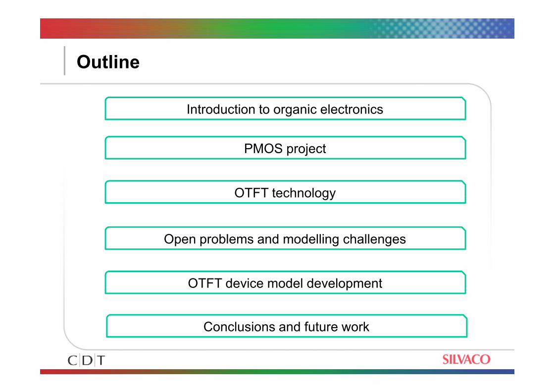
Fast development of organic electronics is supported by applications that
require low cost electronic circuits covering mechanically flexible large areas
These include e-skin, e-paper, e-nose, smart-fabrics, flexible displays,
printed electronics or radio frequency identification tags (RFID).
e-nose
e-skin
Organic electronics can be fabricated using faster and cheaper processes
Basis of the future organic electronic circuits are organic TFTs (OTFTs).
e-nose
Smart fabrics Organic Solar
CellsFlexible display
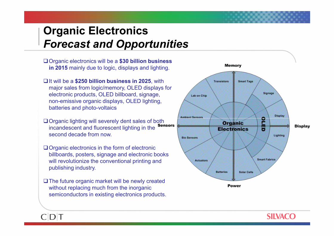
Organic ElectronicsForecast and Opportunities
Organic electronics will be a $30 billion business in 2015 mainly due to logic, displays and lighting.
It will be a $250 billion business in 2025, with
major sales from logic/memory, OLED displays for
electronic products, OLED billboard, signage,
non-emissive organic displays, OLED lighting,
batteries and photo-voltaics
Organic lighting will severely dent sales of both Organic lighting will severely dent sales of both
incandescent and fluorescent lighting in the
second decade from now.
Organic electronics in the form of electronic
billboards, posters, signage and electronic books
will revolutionize the conventional printing and
publishing industry.
The future organic market will be newly created
without replacing much from the inorganic
semiconductors in existing electronics products.
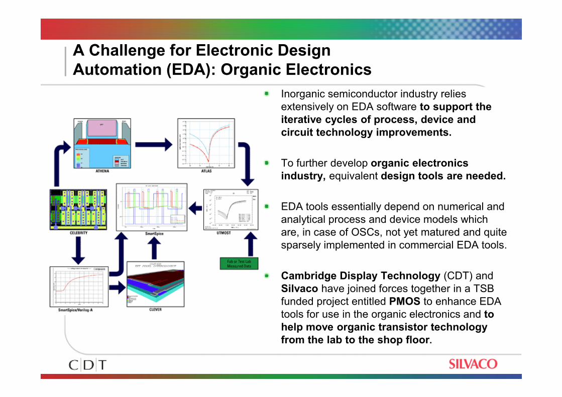
A Challenge for Electronic Design Automation (EDA): Organic Electronics
Inorganic semiconductor industry relies
extensively on EDA software to support the iterative cycles of process, device and circuit technology improvements.
To further develop organic electronics industry, equivalent design tools are needed.
EDA tools essentially depend on numerical and
analytical process and device models which
are, in case of OSCs, not yet matured and quite
sparsely implemented in commercial EDA tools.
Cambridge Display Technology (CDT) and
Silvaco have joined forces together in a TSB
funded project entitled PMOS to enhance EDA
tools for use in the organic electronics and to help move organic transistor technology from the lab to the shop floor.
PMOS ProjectOn Physical Modelling of Organic Semiconductors
Cambridge Display Technology (CDT)
Expert in polymer light emitting diode (PLED) technologies
Leader in development of solution processable (printable) organic
semiconductors for display fabrication
Expertise in development of PLED materials and deposition processes
Silvaco
Leading provider of TCAD and EDA software for IC design
Project partners
Leading provider of TCAD and EDA software for IC design
Provides established products for TCAD process and device simulation, spice
parameter extraction, circuit simulation, custom IC design and verification
Project activities• Device fabrication/measurements/testing
• TCAD model development
• Spice model development
• Measurements and modelling of device reliability and aging effects
• The focus is on display device (oled) drivers as these will be the first largescale organic semiconductor products.
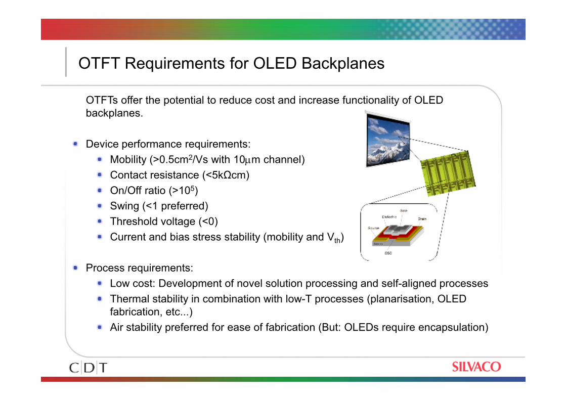
OTFT Requirements for OLED Backplanes
OTFTs offer the potential to reduce cost and increase functionality of OLED
backplanes.
Device performance requirements:
Mobility (>0.5cm2/Vs with 10µm channel)
Contact resistance (<5kΩcm)
On/Off ratio (>105)
Swing (<1 preferred)Swing (<1 preferred)
Threshold voltage (<0)
Current and bias stress stability (mobility and Vth)
Process requirements:
Low cost: Development of novel solution processing and self-aligned processes
Thermal stability in combination with low-T processes (planarisation, OLED
fabrication, etc...)
Air stability preferred for ease of fabrication (But: OLEDs require encapsulation)
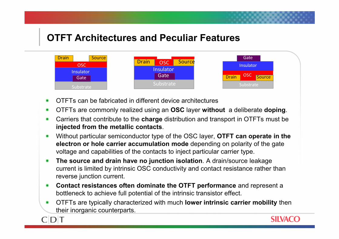
OTFT Architectures and Peculiar Features
OTFTs can be fabricated in different device architectures
OTFTs are commonly realized using an OSC layer without a deliberate doping.
Carriers that contribute to the charge distribution and transport in OTFTs must be
Drain Source
OSC
Insulator
Gate
SubstrateSubstrate
Gate
Insulator
Drain SourceOSC
Substrate
Gate
Insulator
Drain SourceOSC
Carriers that contribute to the charge distribution and transport in OTFTs must be
injected from the metallic contacts.
Without particular semiconductor type of the OSC layer, OTFT can operate in the electron or hole carrier accumulation mode depending on polarity of the gate
voltage and capabilities of the contacts to inject particular carrier type.
The source and drain have no junction isolation. A drain/source leakage
current is limited by intrinsic OSC conductivity and contact resistance rather than
reverse junction current.
Contact resistances often dominate the OTFT performance and represent a
bottleneck to achieve full potential of the intrinsic transistor effect.
OTFTs are typically characterized with much lower intrinsic carrier mobility then
their inorganic counterparts.
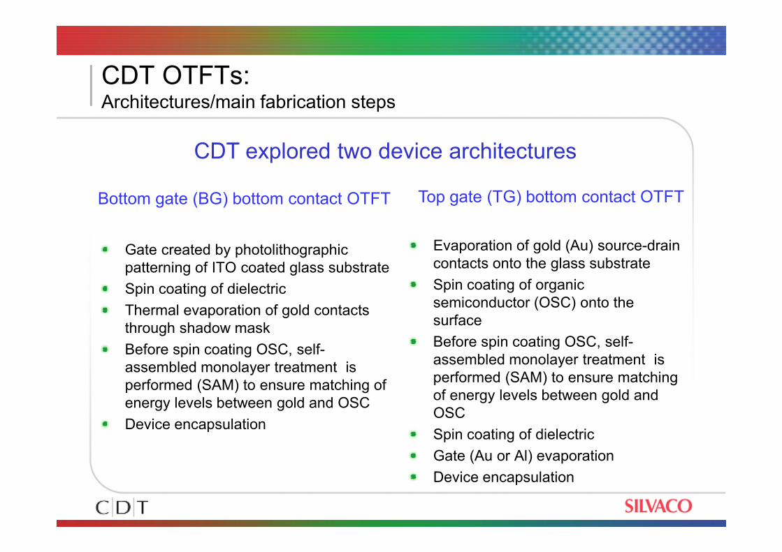
CDT OTFTs:Architectures/main fabrication steps
Bottom gate (BG) bottom contact OTFT Top gate (TG) bottom contact OTFT
Gate created by photolithographic
patterning of ITO coated glass substrate
Evaporation of gold (Au) source-drain
contacts onto the glass substrate
Spin coating of organic
CDT explored two device architectures
Spin coating of dielectric
Thermal evaporation of gold contacts
through shadow mask
Before spin coating OSC, self-
assembled monolayer treatment is
performed (SAM) to ensure matching of
energy levels between gold and OSC
Device encapsulation
Spin coating of organic
semiconductor (OSC) onto the
surface
Before spin coating OSC, self-
assembled monolayer treatment is
performed (SAM) to ensure matching
of energy levels between gold and
OSC
Spin coating of dielectric
Gate (Au or Al) evaporation
Device encapsulation
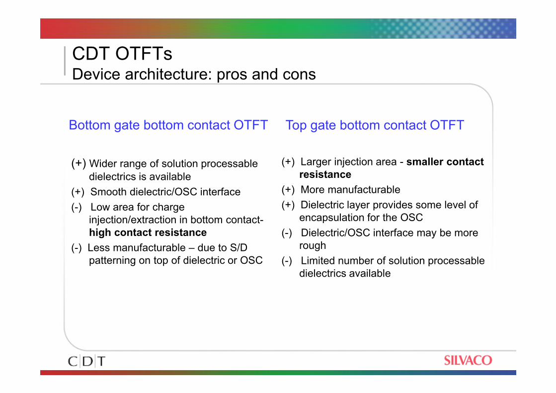
CDT OTFTsDevice architecture: pros and cons
(+) Wider range of solution processable
dielectrics is available
(+) Smooth dielectric/OSC interface
Bottom gate bottom contact OTFT Top gate bottom contact OTFT
(+) Larger injection area - smaller contact resistance
(+) More manufacturable(+) Smooth dielectric/OSC interface
(-) Low area for charge
injection/extraction in bottom contact-
high contact resistance
(-) Less manufacturable – due to S/D
patterning on top of dielectric or OSC
(+) Dielectric layer provides some level of
encapsulation for the OSC
(-) Dielectric/OSC interface may be more
rough
(-) Limited number of solution processable
dielectrics available
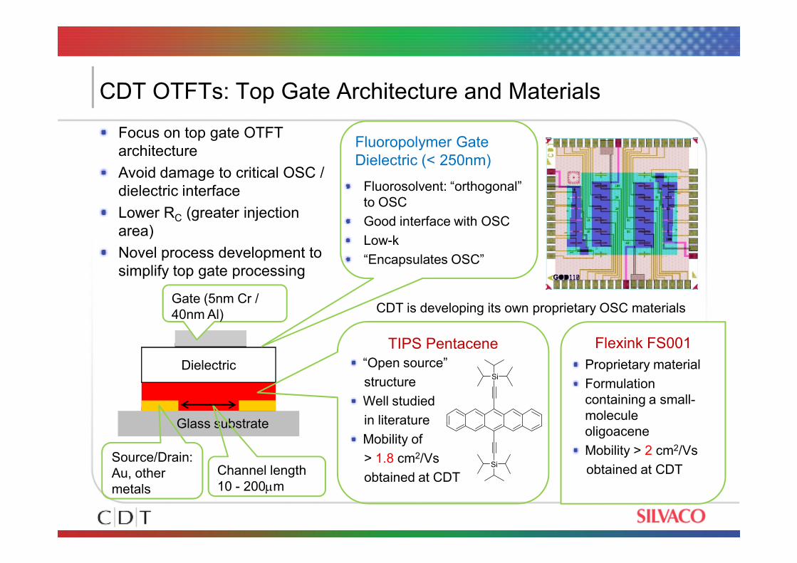
CDT OTFTs: Top Gate Architecture and Materials
Fluorosolvent: “orthogonal”
to OSC
Good interface with OSC
Low-k
“Encapsulates OSC”
Fluoropolymer Gate
Dielectric (< 250nm)
Focus on top gate OTFT
architecture
Avoid damage to critical OSC /
dielectric interface
Lower RC (greater injection
area)
Novel process development to
simplify top gate processing
Si
Si
“Open source”
structure
Well studied
in literature
Mobility of
> 1.8 cm2/Vs
obtained at CDT
Dielectric
Glass substrate
Gate (5nm Cr /
40nm Al)
TIPS Pentacene
Channel length
10 - 200µm
Flexink FS001
Proprietary material
Formulation
containing a small-
molecule
oligoacene
Mobility > 2 cm2/Vs
obtained at CDTSource/Drain:
Au, other
metals
CDT is developing its own proprietary OSC materials
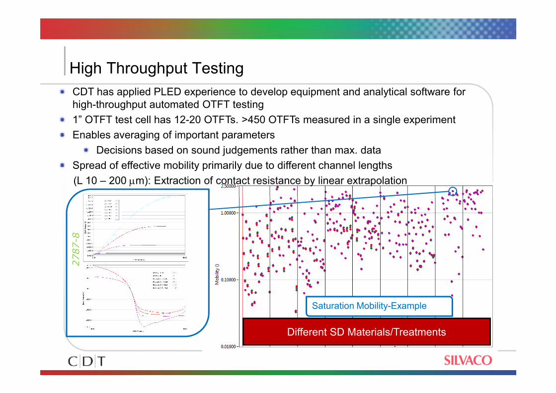
High Throughput Testing
CDT has applied PLED experience to develop equipment and analytical software for
high-throughput automated OTFT testing
1” OTFT test cell has 12-20 OTFTs. >450 OTFTs measured in a single experiment
Enables averaging of important parameters
Decisions based on sound judgements rather than max. data
Spread of effective mobility primarily due to different channel lengths
(L 10 – 200 µm): Extraction of contact resistance by linear extrapolation
2787-8
Different SD Materials/Treatments
Saturation Mobility-Example
Organic TFTsModelling challenges/open problems
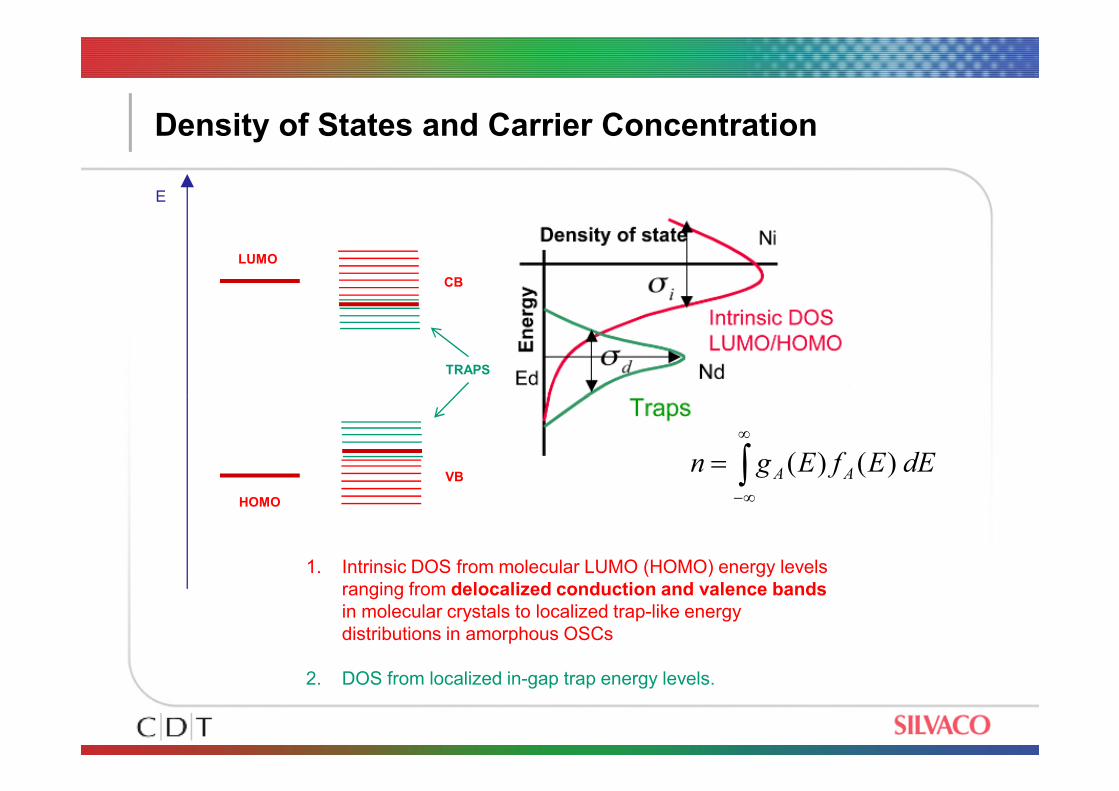
Density of States and Carrier Concentration
LUMO
E
TRAPS
CB
∫∞
∞−
= dEEfEgn AA )()(
1. Intrinsic DOS from molecular LUMO (HOMO) energy levels
ranging from delocalized conduction and valence bandsin molecular crystals to localized trap-like energy
distributions in amorphous OSCs
2. DOS from localized in-gap trap energy levels.
HOMO
VB
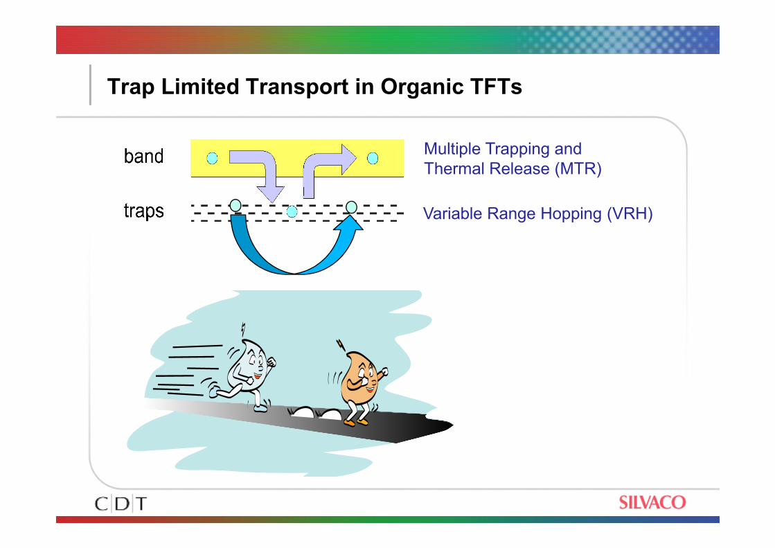
Trap Limited Transport in Organic TFTs
Variable Range Hopping (VRH)
Multiple Trapping and
Thermal Release (MTR)
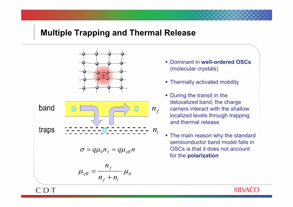
Multiple Trapping and Thermal Release
Dominant in well-ordered OSCs(molecular crystals)
Thermally activated mobility
During the transit in the
delocalized band, the charge
n
nqnq f eff0 µµσ ==
0eff µµ ⋅+
=tf
f
nn
n
delocalized band, the charge
carriers interact with the shallow
localized levels through trapping
and thermal release
The main reason why the standard
semiconductor band model fails in
OSCs is that it does not account
for the polarization
fn
tn
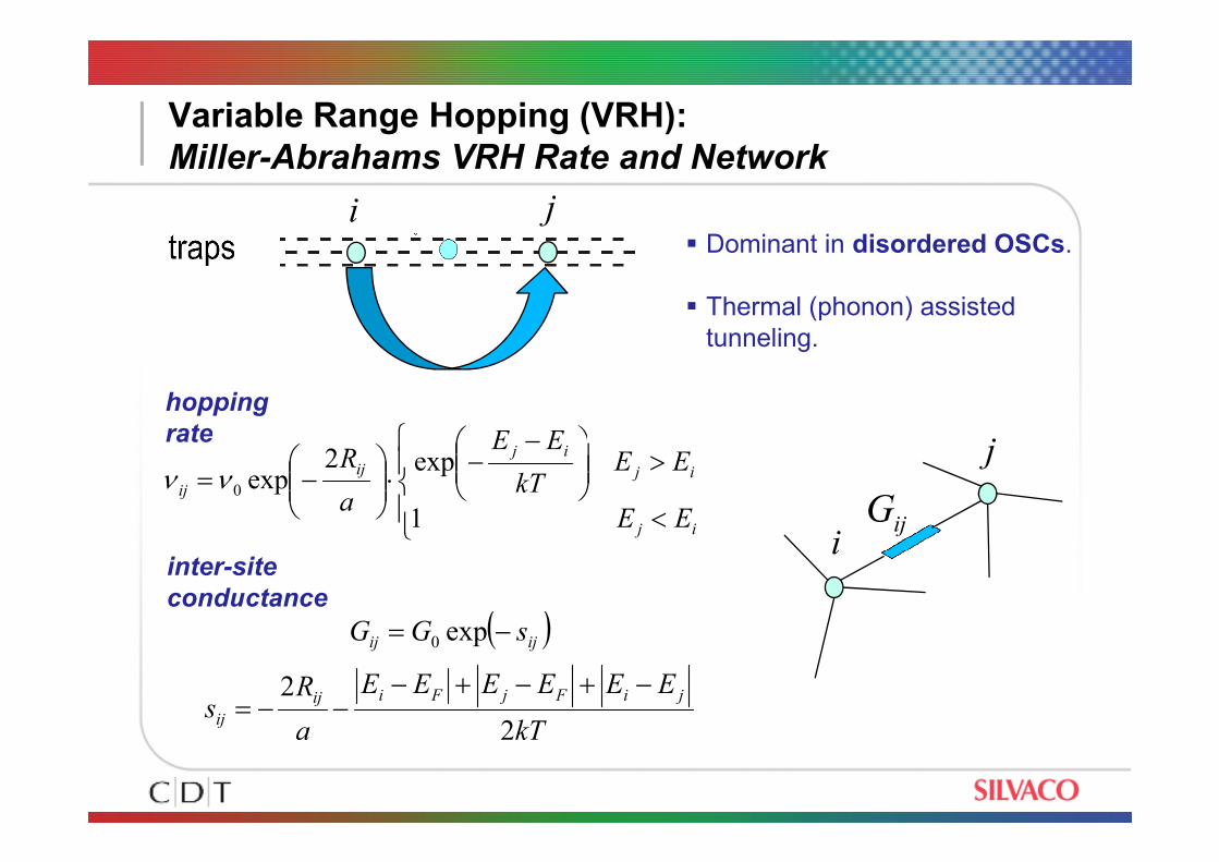
Variable Range Hopping (VRH):Miller-Abrahams VRH Rate and Network
Dominant in disordered OSCs.
Thermal (phonon) assisted
tunneling.
− EE
i j
hopping
ratej
<
>
−−
⋅
−=
ij
ij
ijij
ij
EE
EEkT
EE
a
R
1
exp2exp0νν
rate
( )
kT
EEEEEE
a
Rs
sGG
jiFjFiij
ij
ijij
2
2
exp0
−+−+−−−=
−=
inter-site
conductance
j
iijG
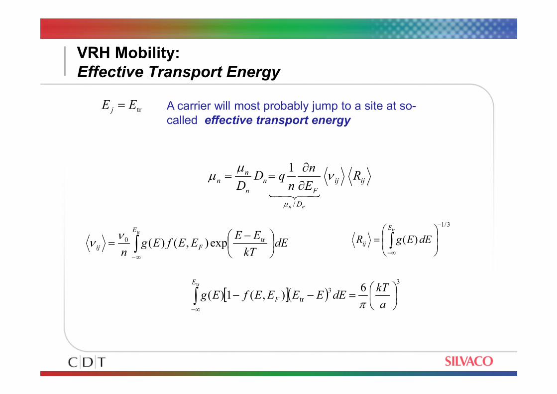
VRH Mobility: Effective Transport Energy
trEE j = A carrier will most probably jump to a site at so-
called effective transport energy
ijij
F
n
n
nn R
E
n
nqD
Dν
µµ
43421
1
∂∂
==
Dnnµ43421
/
3/1tr
)(
−
∞−
= ∫
E
ij dEEgRdEkT
EEEEfEg
n
E
Fij
−= ∫
∞−
tr0 exp),()(trν
ν
[ ]( )3
3
tr
6),(1)(
tr
=−−∫∞− a
kTdEEEEEfEg
E
F π
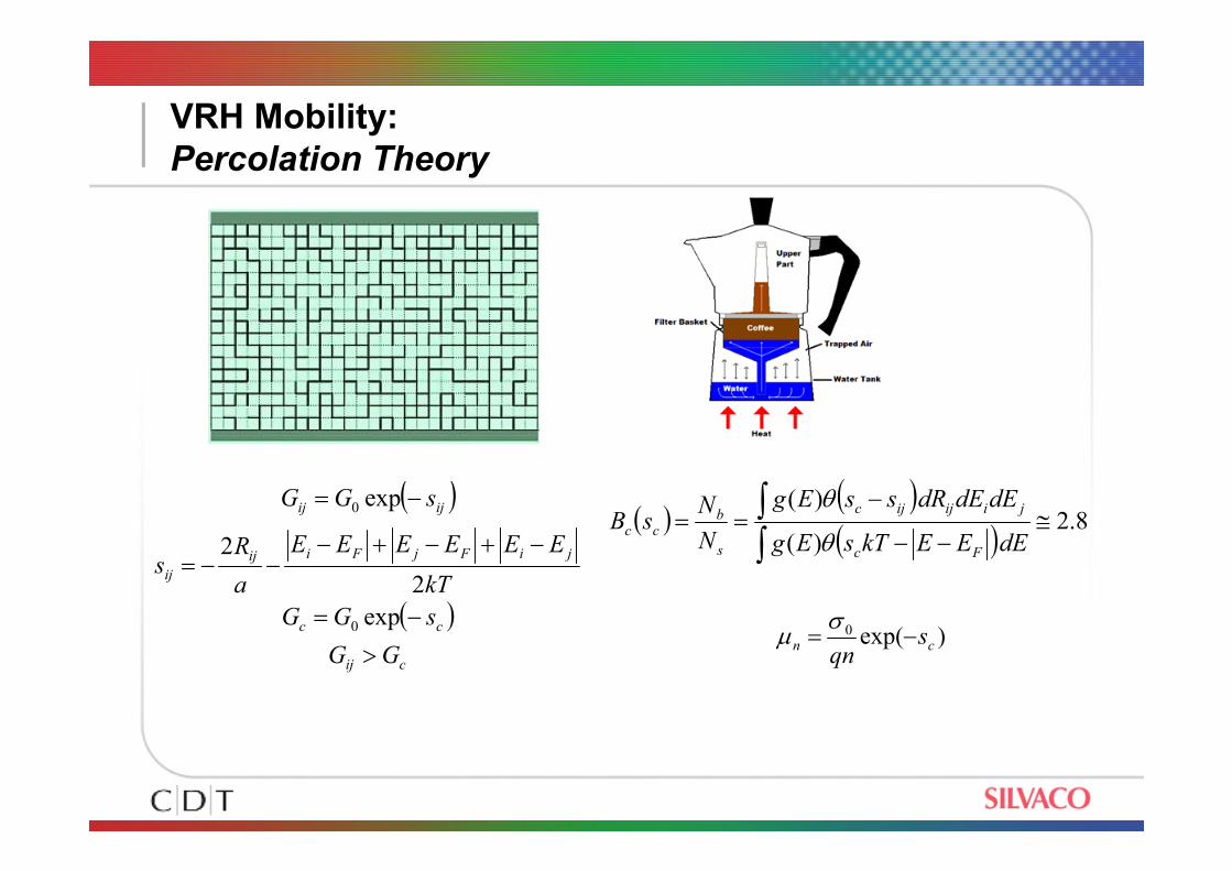
VRH Mobility:Percolation Theory
( )( )( )
8.2)(
)(≅
−−
−==∫∫
dEEEkTsEg
dEdEdRssEg
sB
Fc
jiijijc
s
bcc
θ
θ
)exp(0cn s
qn−=
σµ
( )
( )cij
cc
jiFjFiij
ij
ijij
GG
sGG
kT
EEEEEE
a
Rs
sGG
>
−=
−+−+−−−=
−=
exp
2
2
exp
0
0
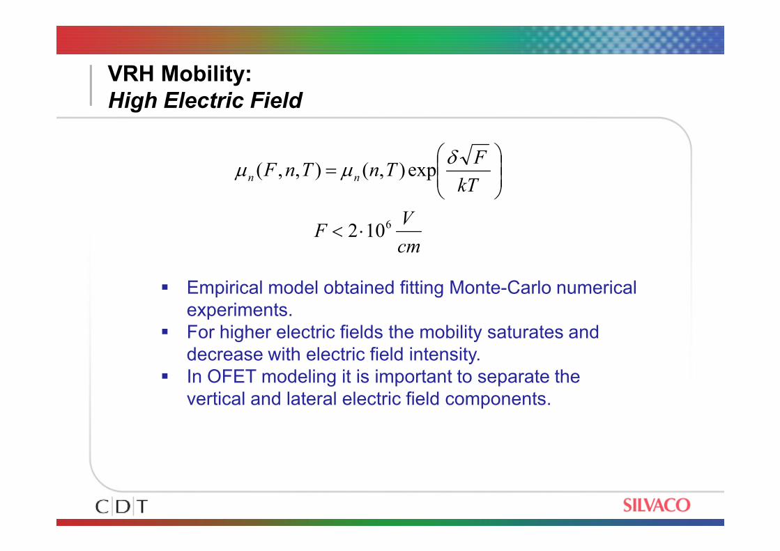
VRH Mobility:High Electric Field
cm
VF
kT
FTnTnF nn
6102
exp),(),,(
⋅<
=
δµµ
Empirical model obtained fitting Monte-Carlo numerical
experiments.
For higher electric fields the mobility saturates and
decrease with electric field intensity.
In OFET modeling it is important to separate the
vertical and lateral electric field components.
OTFT Model Development
Compact modelling (parametric)TCAD modellling (numerical)
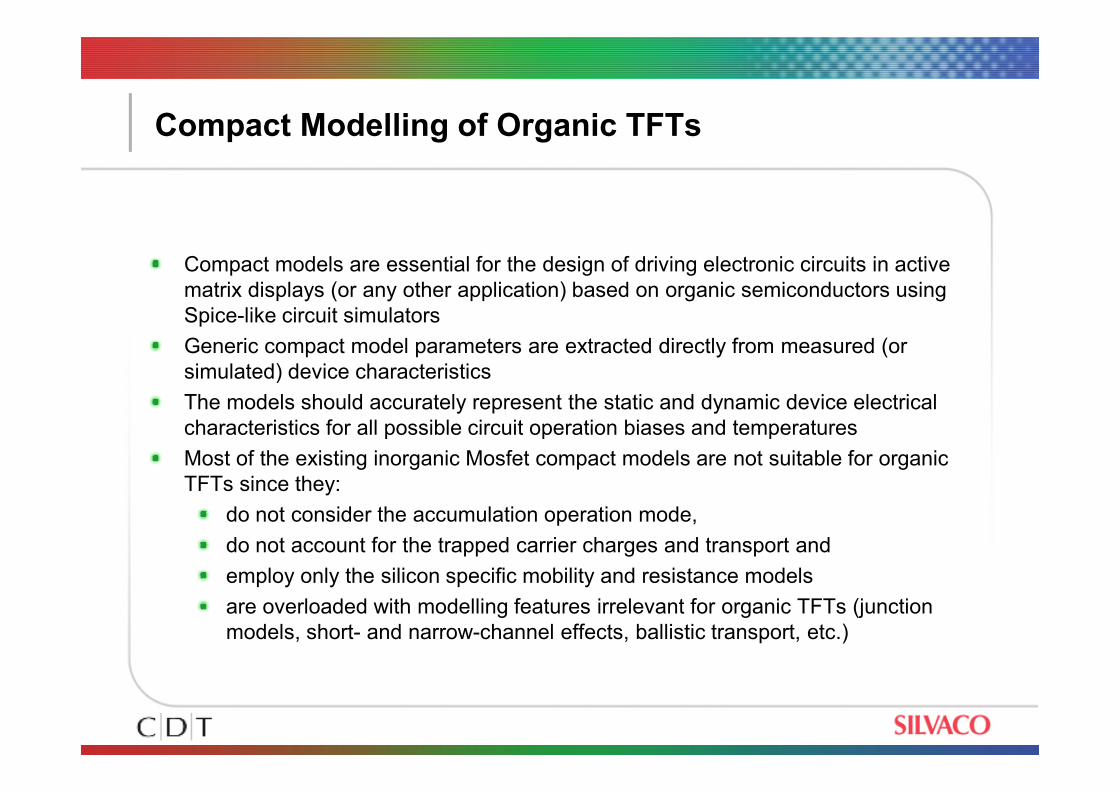
Compact Modelling of Organic TFTs
Compact models are essential for the design of driving electronic circuits in active
matrix displays (or any other application) based on organic semiconductors using
Spice-like circuit simulators
Generic compact model parameters are extracted directly from measured (or
simulated) device characteristics
The models should accurately represent the static and dynamic device electrical The models should accurately represent the static and dynamic device electrical
characteristics for all possible circuit operation biases and temperatures
Most of the existing inorganic Mosfet compact models are not suitable for organic
TFTs since they:
do not consider the accumulation operation mode,
do not account for the trapped carrier charges and transport and
employ only the silicon specific mobility and resistance models
are overloaded with modelling features irrelevant for organic TFTs (junction
models, short- and narrow-channel effects, ballistic transport, etc.)
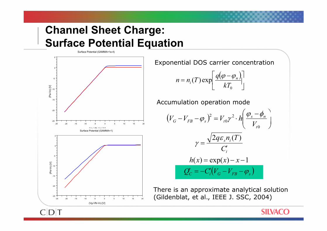
Channel Sheet Charge: Surface Potential Equation
( ) nshVVVφϕ
γϕ
−
⋅=−− 22
-20
-15
-10
-5
0
5
Surface Potential (GAMMA=1e-4)(P
si-V
c)
[V]
( )
−=
0
exp)(kT
qTnn n
i
ϕϕ
Exponential DOS carrier concentration
Accumulation operation mode
( )
( )sFBGiC
i
is
t
nstsFBG
VVCQ
xxxh
C
Tnq
VhVVV
ϕ
εγ
φϕγϕ
−−′−=′
−−=
′=
−⋅=−−
1)exp()(
)(2
0
2
0
2
-25 -20 -15 -10 -5 0 5 10 15 20
-25
(Vg-Vfb-Vc) [V]
-25 -20 -15 -10 -5 0 5 10 15 20
-25
-20
-15
-10
-5
0
5
Surface Potential (GAMMA=1)
(Vg-Vfb-Vc) [V]
(Psi-V
c)
[V]
There is an approximate analytical solution (Gildenblat, et al., IEEE J. SSC, 2004)
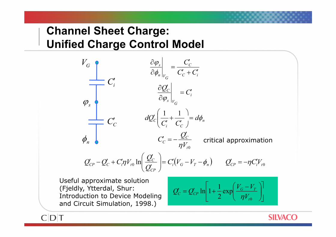
Channel Sheet Charge: Unified Charge Control Model
11nC
i
GVs
C
iC
C
GVn
s
dQd
CQ
CC
C
=
′+′
′
′=∂
′∂
′+′′
=∂∂
φ
ϕ
φϕ
GV
sϕ
iC′
C′
( ) 00
0
ln tiCPnTGi
CP
CtiCCP
t
CC
n
Ci
C
VCQVVCQ
QVCQQ
V
QC
dCC
Qd
′−=′−−′=
′′
′+′−′
′−=′
=
′
+′
′
ηφη
η
φ
nφ
CC′
−+′=′
0
exp2
11ln
t
TGCPC
V
VVQQ
η
Useful approximate solution (Fjeldly, Ytterdal, Shur: Introduction to Device Modeling and Circuit Simulation, 1998.)
critical approximation
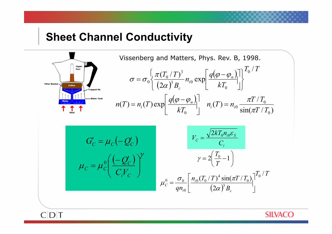
Sheet Channel Conductivity
( )( )
( ))/sin(
/)(exp)()(
/
exp2
)/(
0
00
0
0
0
03
3
00
TT
TTnTn
kT
qTnTn
TT
kT
qn
B
TT
iin
i
ni
c
ππϕϕ
ϕϕα
πσσ
=
−=
−=
Vissenberg and Matters, Phys. Rev. B, 1998.
( )
( ) γµµ
µ
′−=
′−=′
Ci
CCC
CCC
VC
Q
QG
0
( )
TT
B
TTTTn
qn
T
T
C
nkTV
c
i
i
C
i
Si
C
/
2
)/sin()/(
12
2
0
3
0
4
00
0
00
0
00
=
−=
=
απσ
µ
γ
ε
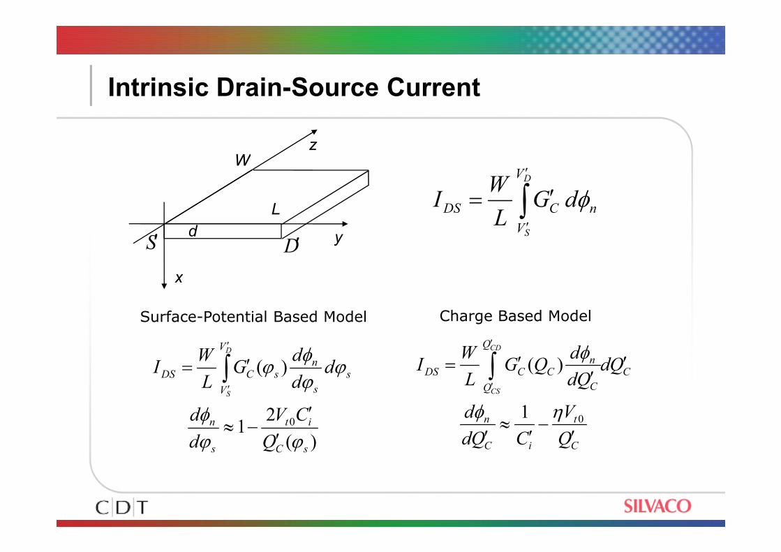
Intrinsic Drain-Source Current
x
y
zW
L
S′ D′d
∫′
′
′=D
S
V
V
nCDS dGL
WI φ
x
)(
21
)(
0
sC
it
s
n
V
V
s
s
nsCDS
Q
CV
d
d
dd
dG
L
WI
D
S
ϕϕφ
ϕϕφ
ϕ
′′
−≈
′= ∫′
′
C
t
iC
n
C
Q
Q C
nCCDS
Q
V
CQd
d
QdQd
dQG
L
WI
CD
CS
′−′
≈′
′′
′= ∫′
′
01
)(
ηφ
φ
Surface-Potential Based Model Charge Based Model
Parametric approachSOTFT - Surface potential based OTFT model
A surface potential based compact model for organic TFTs (SOTFT) has been developed
The model provides physical description of the currents and charges based on the accurate evaluation of electrical potential at the insulator-semiconductor interface
It employs the physical mobility description based on exponential DOS and It employs the physical mobility description based on exponential DOS and variable range hopping transport
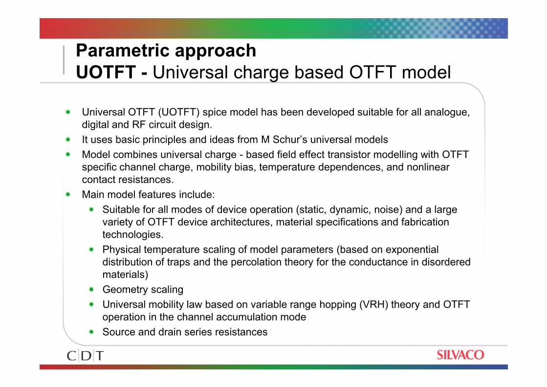
Parametric approachUOTFT - Universal charge based OTFT model
Universal OTFT (UOTFT) spice model has been developed suitable for all analogue,
digital and RF circuit design.
It uses basic principles and ideas from M Schur’s universal models
Model combines universal charge - based field effect transistor modelling with OTFT
specific channel charge, mobility bias, temperature dependences, and nonlinear
contact resistances.
Main model features include:Main model features include:
Suitable for all modes of device operation (static, dynamic, noise) and a large
variety of OTFT device architectures, material specifications and fabrication
technologies.
Physical temperature scaling of model parameters (based on exponential
distribution of traps and the percolation theory for the conductance in disordered
materials)
Geometry scaling
Universal mobility law based on variable range hopping (VRH) theory and OTFT
operation in the channel accumulation mode
Source and drain series resistances
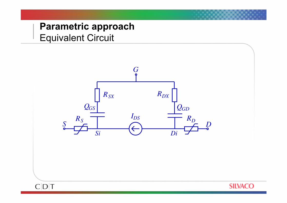
Parametric approachEquivalent Circuit
RSX
G
Q
RDX
DS
Si Di
IDS
GDQQGS
RS RD
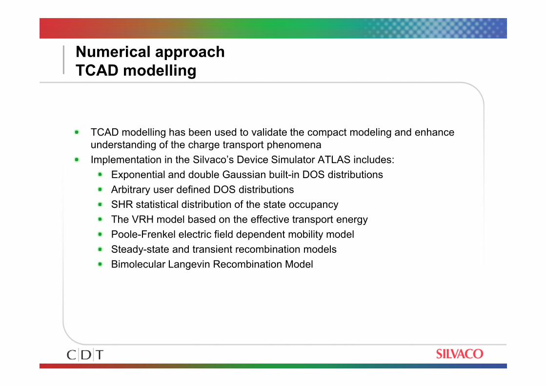
Numerical approachTCAD modelling
TCAD modelling has been used to validate the compact modeling and enhance
understanding of the charge transport phenomena
Implementation in the Silvaco’s Device Simulator ATLAS includes:
Exponential and double Gaussian built-in DOS distributions
Arbitrary user defined DOS distributionsArbitrary user defined DOS distributions
SHR statistical distribution of the state occupancy
The VRH model based on the effective transport energy
Poole-Frenkel electric field dependent mobility model
Steady-state and transient recombination models
Bimolecular Langevin Recombination Model
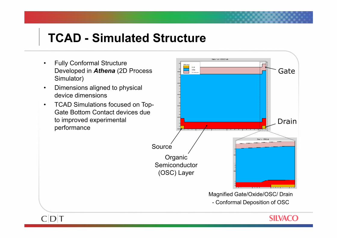
TCAD - Simulated Structure
Gate
Drain
• Fully Conformal Structure
Developed in Athena (2D Process
Simulator)
• Dimensions aligned to physical
device dimensions
• TCAD Simulations focused on Top-
Gate Bottom Contact devices due
to improved experimental
Source
Organic
Semiconductor
(OSC) Layer
Drain
Magnified Gate/Oxide/OSC/ Drain
- Conformal Deposition of OSC
to improved experimental
performance
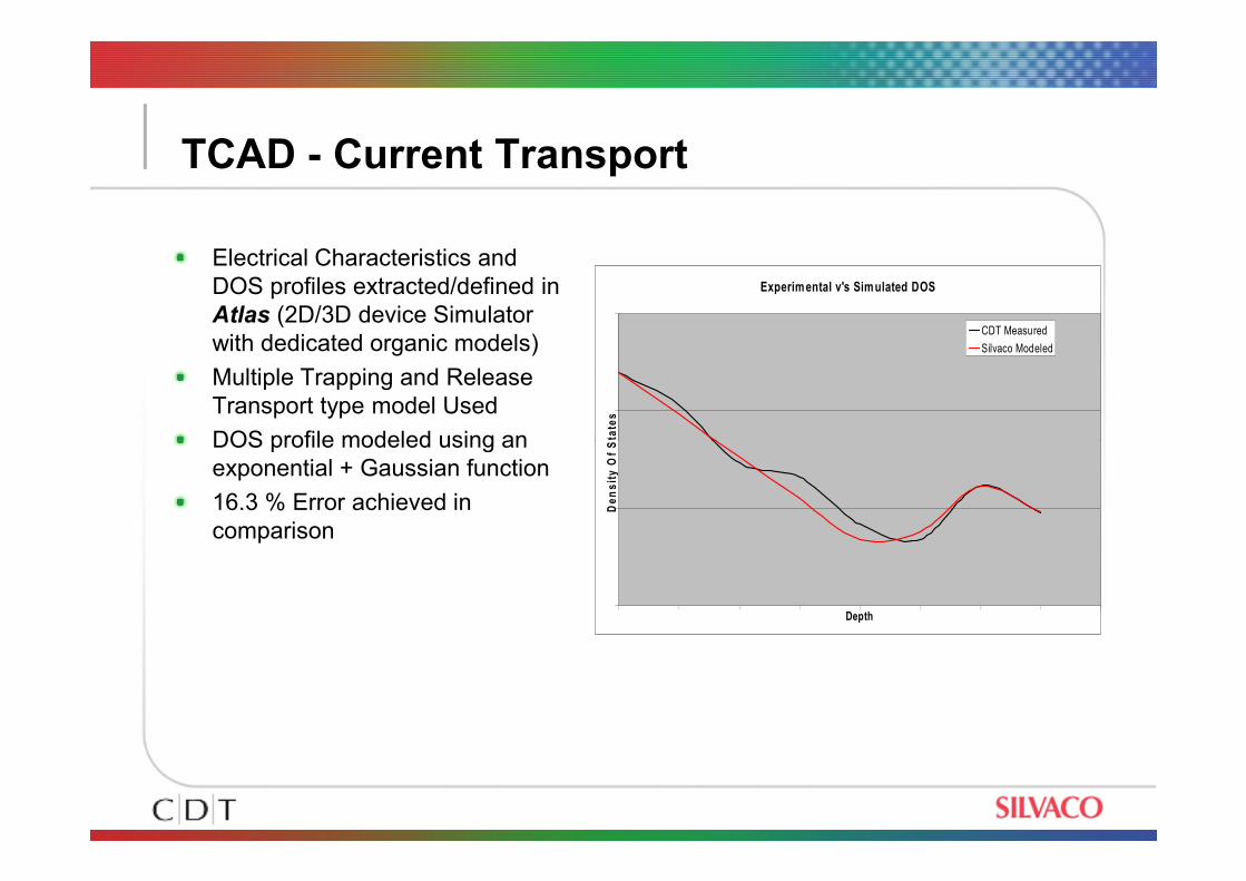
TCAD - Current Transport
Electrical Characteristics and
DOS profiles extracted/defined in
Atlas (2D/3D device Simulator
with dedicated organic models)
Multiple Trapping and Release
Transport type model Used
DOS profile modeled using an
Experimental v's Simulated DOS
Density O
f Sta
tes
CDT Measured
Silvaco Modeled
DOS profile modeled using an
exponential + Gaussian function
16.3 % Error achieved in
comparison
DepthDensity O
f Sta
tes
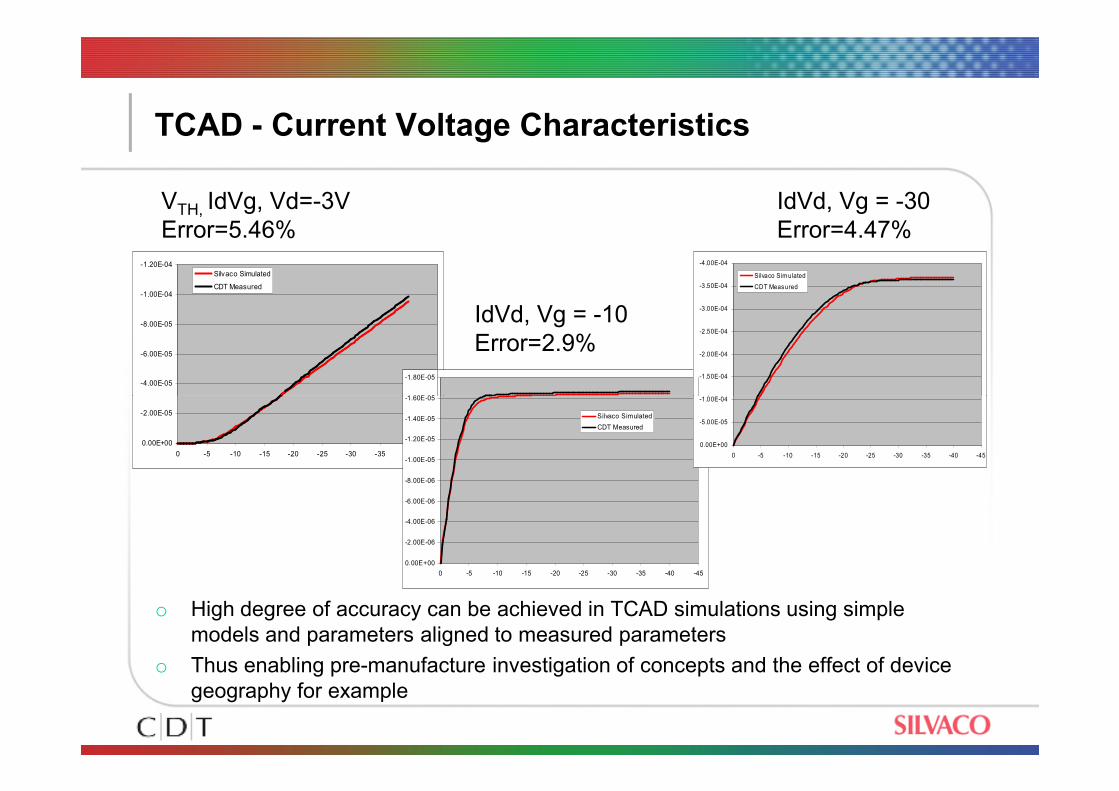
TCAD - Current Voltage Characteristics
-1.20E-04
-1.00E-04
-8.00E-05
-6.00E-05
-4.00E-05
Silvaco Simulated
CDT Measured
VTH, IdVg, Vd=-3V
Error=5.46%
-1.80E-05
-1.60E-05
IdVd, Vg = -10
Error=2.9%
IdVd, Vg = -30
Error=4.47%-4.00E-04
-3.50E-04
-3.00E-04
-2.50E-04
-2.00E-04
-1.50E-04
-1.00E-04
Silvaco Simulated
CDT Measured
o High degree of accuracy can be achieved in TCAD simulations using simple
models and parameters aligned to measured parameters
o Thus enabling pre-manufacture investigation of concepts and the effect of device
geography for example
-2.00E-05
0.00E+00
-45-40-35-30-25-20-15-10-50
-1.60E-05
-1.40E-05
-1.20E-05
-1.00E-05
-8.00E-06
-6.00E-06
-4.00E-06
-2.00E-06
0.00E+00
-45-40-35-30-25-20-15-10-50
Silvaco Simulated
CDT Measured
-1.00E-04
-5.00E-05
0.00E+00
-45-40-35-30-25-20-15-10-50
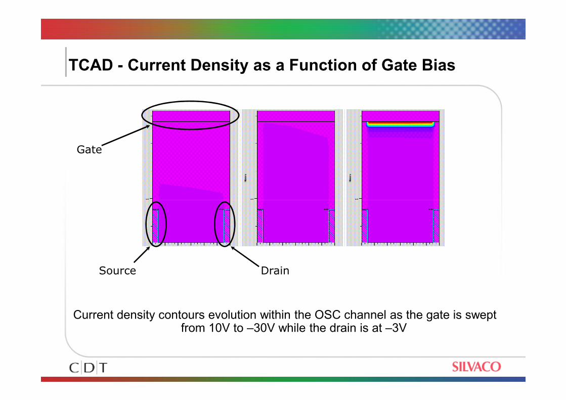
TCAD - Current Density as a Function of Gate Bias
Gate
Current density contours evolution within the OSC channel as the gate is swept from 10V to –30V while the drain is at –3V
Source Drain
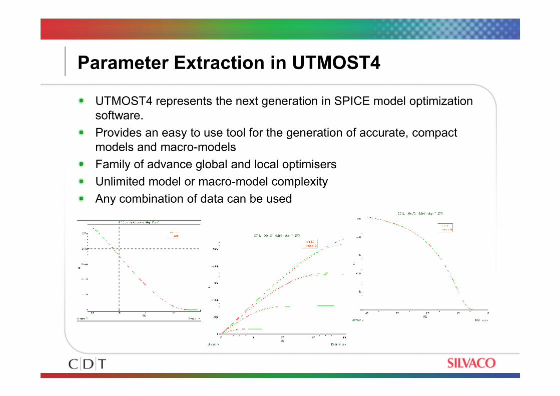
Parameter Extraction in UTMOST4
UTMOST4 represents the next generation in SPICE model optimization
software.
Provides an easy to use tool for the generation of accurate, compact
models and macro-models
Family of advance global and local optimisers
Unlimited model or macro-model complexity
Any combination of data can be usedAny combination of data can be used
Compact model evaluation SOTFT and UOTFT model performance
The performances of SOTFT model and UOTFT model are verified with measured
advanced OTFT device structures and related TCAD organic simulations in ATLAS.
UOTFT model is implemented into Simucad’s model library and made accessible as
a TFT model level 37.
Equivalent circuit and external components match the existing inorganic TFT models
(level 35 and 36).
UOTFT model performance is verified on various OTFT technologies and device
architectures.
Figures in the following slides compare the simulated with the measured data from
the bottom-gate bottom contact OTFT device (for both models)
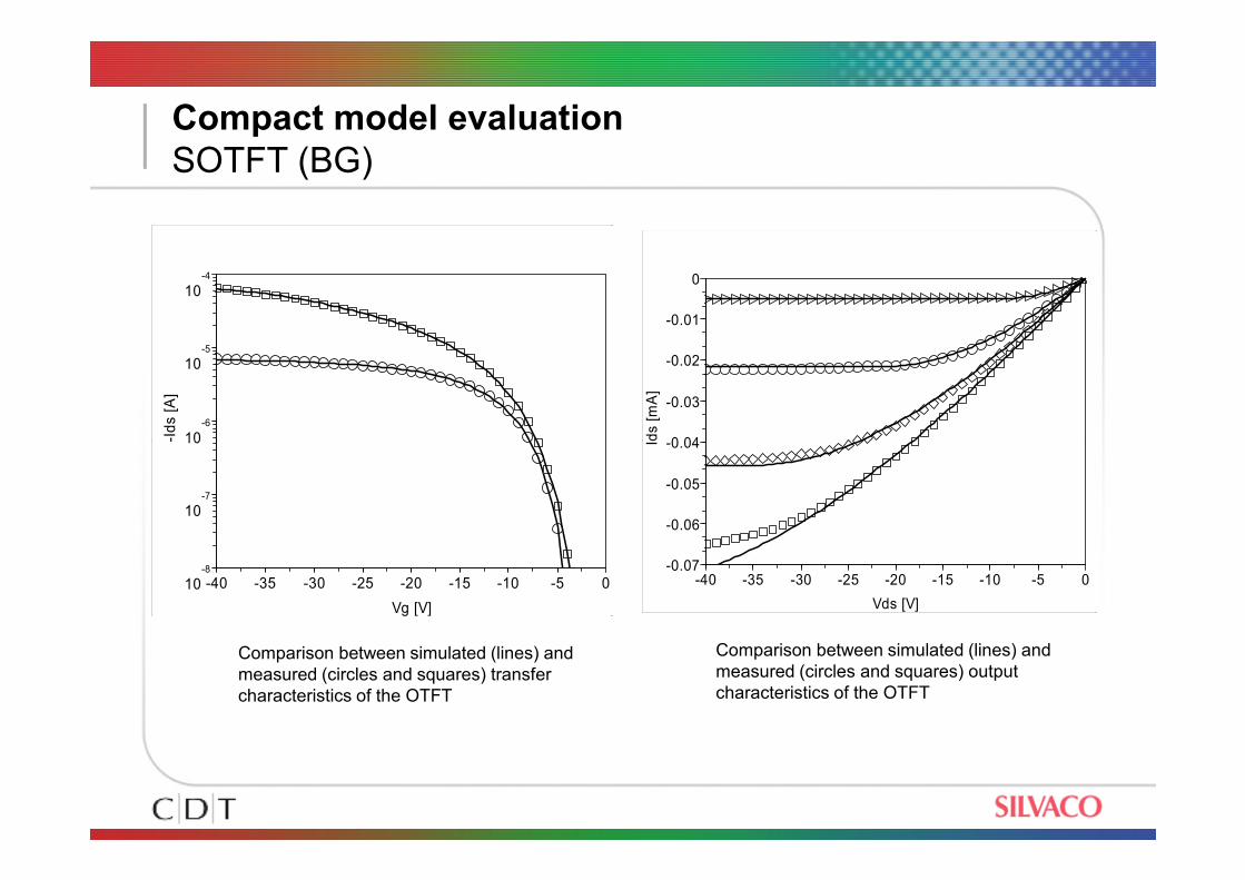
Compact model evaluation SOTFT (BG)
-6
10
-5
10
-4
10
-Id
s [
A]
-0.04
-0.03
-0.02
-0.01
0
Ids [
mA
]
-40 -35 -30 -25 -20 -15 -10 -5 0-8
10
-7
10
10
Vg [V]
-Id
s [
A]
-40 -35 -30 -25 -20 -15 -10 -5 0-0.07
-0.06
-0.05
-0.04
Vds [V]
Ids [
mA
]Comparison between simulated (lines) and
measured (circles and squares) transfer
characteristics of the OTFT
Comparison between simulated (lines) and
measured (circles and squares) output
characteristics of the OTFT
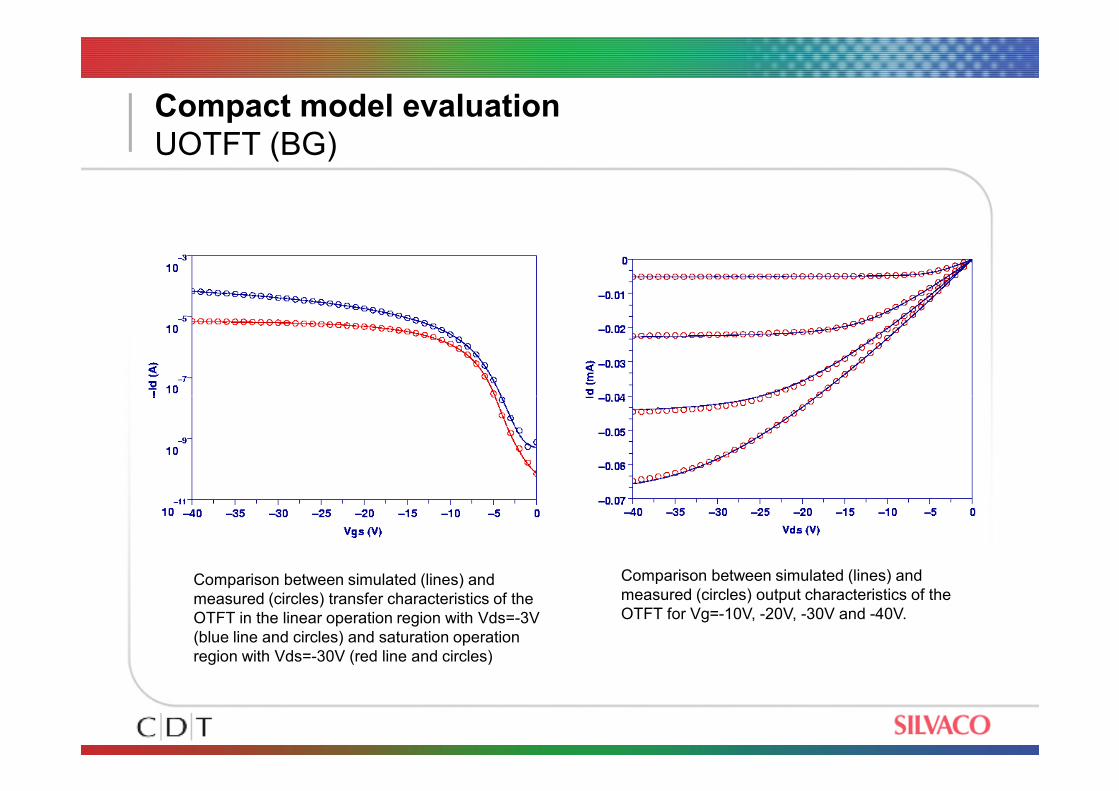
Compact model evaluation UOTFT (BG)
Comparison between simulated (lines) and
measured (circles) transfer characteristics of the
OTFT in the linear operation region with Vds=-3V
(blue line and circles) and saturation operation
region with Vds=-30V (red line and circles)
Comparison between simulated (lines) and
measured (circles) output characteristics of the
OTFT for Vg=-10V, -20V, -30V and -40V.
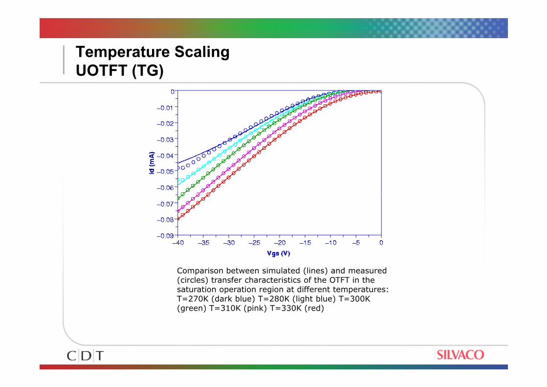
Temperature ScalingUOTFT (TG)
Comparison between simulated (lines) and measured (circles) transfer characteristics of the OTFT in the saturation operation region at different temperatures: T=270K (dark blue) T=280K (light blue) T=300K (green) T=310K (pink) T=330K (red)
Conclusions
EDA tools with accurate and predictive physical OTFT models are crucial
for speeding up the optimisation of device performance and enable organic
circuit design
Demonstrated that application of advanced models for a charge transport
and mobility behaviour in Atlas can provide accurate physical modelling of
OTFT devices
TCAD model development
Explores the effect of design parameters and performs optimisation
procedure
Enables testing of a layout and all geometry, material and process related
issues
Compact model development
Developed compact models can provide a very good fit to the measured
transfer and output device data at various temperatures
Future works
TCADInvestigate a computationally reasonable approach to incorporate
percolation theory mobility models with arbitrary DOS distribution for TCAD
device modeling
Mixed mode simulation
Aging
Compact modellingExtend a model to account for the bias dependent contact resistances, gate
tunelling, effect of interface trap states
Model a dynamic device behaviour
Handle aging and hysteresis of the OTFT characteristics within the model
and the corresponding circuit design
Acknowledgement
We want to thank Prof. Iniguez and his group for valuable
recommendations regarding compact organic TFT
modelling.
This work is supported by the UK Technology Strategy
Board through the PMOS project TP/J2519J.