Embed Size (px)
Citation preview

Journal of
Low Power Electronicsand Applications
Article
Models and Techniques for Temperature RobustSystems on a Reconfigurable Platform
Sahil Shah 1, Hakan Toreyin 2, Jennifer Hasler 1,* and Aishwarya Natarajan 1
1 Department of Electrical and Computer Engineering, Georgia Institute of Technology,Atlanta, GA 30332, USA; [email protected] (S.S.); [email protected] (A.N.)
2 Department of Electrical and Computer Engineering, San Diego State University,San Diego, CA 92182, USA; [email protected]
* Correspondence: [email protected]; Tel.: +1-404-894-4641
Received: 31 July 2017; Accepted: 26 August 2017; Published: 30 August 2017
Abstract: This paper investigates the variability of various circuits and systems over temperature andpresents several methods to improve their performance over temperature. The work demonstratesuse of large scale reconfigurable System-On-Chip (SOC) for reducing the variability of circuitsand systems compiled on a Floating Gate (FG) based Field Programmable Analog Array (FPAA).Temperature dependencies of circuits are modeled using an open-source simulator built in theScilab/XCOS environment and the results are compared with measurement data obtained fromthe FPAA. This comparison gives further insight into the temperature dependence of variouscircuits and signal processing systems and allows us to compensate as well as predict their behavior.Also, the work presents several different current and voltage references that could help in reducingthe variability caused due to changes in temperature. These references are standard blocks inthe Scilab/Xcos environment that could be easily compiled on the FPAA. An FG based currentreference is then used for biasing a 12× 1 Vector Matrix Multiplication (VMM) circuit and a secondorder Gm − C bandpass filter to demonstrate the compilation and usage of these voltage/currentreference in a reconfigurable fabric. The large scale FG FPAA presented here is fabricated in a 350 nmCMOS process.
Keywords: circuits and system; temperature dependence; reference generator; FPAA
1. Analog Processing and Temperature Dependence
The number of systems combining elements from within and among the emerging technologiesof sensors, communications, and robotics grows every day. The computational abilities of thesesystems affect the overall system performance through various aspects (e.g., functionality, battery-life,foot-print, etc.). Traditionally most computational tasks have been performed in the digital domain,which can achieve high resolution computation at the cost of high power consumption [1]. For systemswith a limited power budget, however, low-power, real-time computation techniques have beensought after. Accordingly, analog-signal-processing has been used extensively as an energy-efficientalternative to digital options [2–4].
Recent mixed-mode large-scale Field-Programmable Analog Array (FPAA) enables advancedfunctionality for a wide spectrum of sensor applications [5]. These FPAAs combine the energy-efficiency,reconfigurability, and programmability of floating-gate-based analog signal processing with the precisionand compatibility of digital, thereby a variety of analog circuitry implemented on FPAAs serve as buildingblocks of more complex signal processing functions [5].
Many of the systems that can benefit from the computational power of an FPAA need to operateover a range of environments and temperatures. For instance, modern ubiquitous medical healthassessment systems use physiologic signals collected from ambulatory subjects during daily outdoor
J. Low Power Electron. Appl. 2017, 7, 21; doi:10.3390/jlpea7030021 www.mdpi.com/journal/jlpea

J. Low Power Electron. Appl. 2017, 7, 21 2 of 14
activities [6]. Likewise, point-of-care diagnostics platforms aiming to achieve lab-quality tests inlow-resource settings, operate in environments with varying ambient temperatures [7,8]. Furthermore,in assisted living applications, sensor networks are used to identify and track the daily activities ofelderly in outdoor settings. For outdoor applications where temperature is not stable, one of the criticalperformance metrics affecting the computation accuracy of the FPAA would be, therefore, robustnessagainst temperature variations.
This work presents a range of techniques and models to estimate and reduce temperaturevariability of various systems. Figure 1 shows the proposed method that a user could follow, dependingon specific application. A range of voltage and current reference generators are available to be compiledon the FPAA to reduce the temperature variability of the system. Here, we propose to use a FloatingGate (FG) as a programmable element to achieve reasonable temperature insensitivity rather thantrimming/single value FG to achieve precision [9]. These references form standard blocks in theopen source tools built in the Scilab/Xcos environment, available online [10,11]. This enables a widerange of programmable structures that could be compiled along with the system. When a userreprograms the system or a circuit, the references as a part of the Xcos design will compile on theFPAA. This work utilizes an Xcos tool simulation model [11] to model circuits’ block temperaturevariation. Temperature measurements were performed using a ZPlus (Cincinnati Sub-Zero ProductsLLC, Sharonville, OH, USA) temperature chamber. For each temperature value, 15 min is allowed toensure that the FPAA die reaches the desired temperature value.
Compile on FPAA with the system
FPAA Fabric
16k x 16 SRAM
µP
DACs
ProgDACVDD
VDD
GNDGND
VDD
VDD
GNDGND GND
VDD
Choose current or voltage references to reduce temperature variability
Command-Word
Recognition
Heart Rate Extraction
Activity Detector
Ultrasound Imaging
Applications
Image Convolution
Acoustic Detection
Circuit Designers
System Designers
EKV Model SimulateDesign with CAB components VDD VDD
GNDGND
Figure 1. Proposed method to reduce temperature variability while compiling a system for a desiredapplication on a FPAA. The tool infrastructure offers flexibility depending on the user. A system designerwould choose from multiple voltage and current references depending on the application [3,4,12,13].Then, the system along with the selected references would be compiled on the FPAA. This wouldenable wide range of programmable and reconfigurable temperature robust systems. In case of a circuitdesigner the FPAA tool infrastructure enables designing a custom reference circuit. The circuit could besimulated, with models based on EKV, before compiling the design on the hardware.
Temperature behavior of programmable circuits in the SoC FPAA will proceed in six stages.A description of the FPAA is presented in Section 2. In Section 3, various temperature models fordevices available in a FPAA is presented. These models are then used to estimate the variation in simplesingle ended circuits in Section 4 and these simulations are compared with measured data. In Section 5,various references are introduced and their variability with temperature is studied. A bootstrap FGreference generator is introduced in Section 5.1. Section 5.2 shows resistorless voltage references thatcan be compiled on the FPAA. Sections 6 and 7 show the performance of various signal processingsystems and circuits over temperature.

J. Low Power Electron. Appl. 2017, 7, 21 3 of 14
2. Field-Programmable Analog Array
An FPAA is a mixed signal FPGA having both analog as well as digital components. The majoradvantage of such SoC over ASIC is prototyping large systems in a cost effective manner and shorteningthe test cycle. The FPAA used in this work has the same architecture described in [5].
Figure 2 shows the general architecture of the FPAA with its elements. The FPAA fabric iscomposed of Computational Analog Block (CAB) and Computational Logic Block (CLB), shownas A and D respectively in Figure 2. The schematic of the CAB elements is shown in the Figure 2,along with the interconnect switch fabric for the FPAA. The CAB consists of various analog elementssuch as OTA, Floating Gate input OTA (FGOTA), nFET current mirrors, transmission gates, capacitors,and NMOS and PMOS transistors. The CAB also consists of an analog shift register that allows formeasuring multiple nodes using a single IO (Input-Output) pad or an analog-to-digital converter(ADC). FPAA uses a floating gate pFET as a basic building block that acts as a nonvolatile switch andalso for biasing various analog elements. The FPAA also consists of an open source microprocessorMSP430 that, along with the programming infrastructure, is used to compile the design on the fabric.Programming infrastructure consists of several 7-bit digital-to-analog converters (DAC) and a 14-bitADC. The programming algorithm, described in detail here [14], uses hot-electron injection andFowler-Nordheim tunneling for programming and erasing the charge on the floating node.
Vdd
VG
VG
VG
VG
VG
VG
VG
VG
VG
VG
VG
VG
VG
VG
CAB Elements
VG=VDAC
8-bit
DAC
GNDGND
VDD
VDD
10 Mohm
VG=VREF
Switch Fabric
A
A
A
A
A
A
A
A
A
A
A
A
A
A
D
D
D
D
D
D
D
D
D
D
D
D
D
D
D
D
D
D
D
D
D
D
D
D
D
D
D
D
D
D
D
D
D
D
D
D
D
D
D
D
D
D
A
A
A
A
A
A
A
A
A
A
A
A
A
A
A
A
A
A
A
A
A
A
A
A
A
A
A
A
D
D
D
D
D
D
D
D
D
D
D
D
D
D
D
D
D
D
D
D
D
D
D
D
D
D
D
D
A
A
A
A
A
A
A
A
A
A
A
A
A
A
A
A
A
A
A
A
A
A
A
A
A
A
A
A
D
D
D
D
D
D
D
D
D
D
D
D
D
D
D
D
D
D
D
D
D
D
D
D
D
D
D
D
A
A
A
A
A
A
A
A
A
A
A
A
A
A
A
A
A
A
A
A
A
A
A
A
A
A
A
A
SRAM
Program: 8k x 16
Data: 8k x 16
MSP430
Open Core
Processor
Memory
Mapped
Registers
DA
Cs
Pro
g D
AC
s
GP I/O
Prog: I V
Ramp ADC
Figure 2. FPAA structure with its components. FPAA fabric is made of computational analog block (A)and computational logic block (D). A part of the FPAA computational analog block (CAB) along withits elements. The switch fabric of the FPAA is made of Floating Gate (FG) elements. Also, the biasing ofOperational Transconductance Amplifier (OTA) is done using a FG pFET transistor. The gate of theseFG pFET transistor could be biased using a 7-bit DAC or a bootstrap voltage reference.
The floating gate input (VG) during the operational mode is held at a constant voltage usingan on-chip DAC. Alternatively, a voltage reference, similar to the one shown in the Figure 2, could becompiled on to the FPAA fabric. The FPAA allows the user to toggle between these two biasing modesas necessary.
3. Modeling Temperature Dependence
A simulation model adapted from the Enz-Krummenacher-Vittoz (EKV) model [15] for all regionsof operation is developed. Based on this model the channel current for a pMOS and an nMOS transistorare governed by the following equations
Id = Ithnmos ln2(
1 + e(κ(Vg−VT0n)−(Vs)+σ(Vd))/2UT)− Ithnmos ln2
(1 + e(κ(Vg−VT0n)−(Vd)+σ(Vs))/2UT
)Id = Ithpmos ln2
(1 + e(κ(VDD−Vg−VT0p)−(VDD−Vs)+σ(VDD−Vd))/2UT
)− Ithpmos ln2
(1 + e(κ(VDD−Vg−VT0p)−(VDD−Vd)+σ(VDD−Vs))/2UT
) (1)
where Ithnmos and Ithpmos are specific currents at threshold voltage given by 2µnmosCox(W/L)U2T/κ
and 2µpmosCox(W/L)U2T/κ, respectively, σ is the drain-induced barrier lowering coefficient, and Vd,
J. Low Power Electron. Appl. 2017, 7, 21 4 of 14
Vs, VT0p, VT0n, and UT are the drain, source, pMOS zero-bias threshold, nMOS zero-bias threshold,and thermal voltages, respectively. Temperature dependence of Id in Equation (1) arises from thresholdvoltages, Ith, and explicit UT . The dependence of threshold voltages on temperature could be modeledusing A1 + A2 ∗ UT . Ith has dependence on temperature due to the mobility (µ) and presence ofU2
T , which could be modeled using Ithr ∗ ( TTr)
a, where a = 0.5. From measured data, shown in the
the Table 1, which showsdIthdT
/Ithr =aTr
(2)
it can be seen that a ≈ 0.6. Here, Tr is the reference temperature (298 K). The variation of VTo isas follows
dVto
dT= −2
κln(
ND√NcNv
)dUTdT
(3)
where Nc and Nv are the effective density of electrons and holes in conduction and valence band,respectively. Their dependence on temperature is T3/2 [16]. This is small compared to the lineardependence to UT term. It should be noted that the model in [15] has more parameters and is muchmore generalized. In the case of Equation (1), the model has a reduced number of parameters, whichallows for faster simulation, with the ability to closely predict data from the FPAA.
Table 1. Comparison of simulated and measured data: Percentage change over 60 ◦C.
Device Measured Simulated
Parameter Threshold Voltage Ith Threshold Voltage Ith
pFET −0.28% −1.7 mV/C 0.2% 2000 ppm/C −0.27% −1.7 mV/C 0.17% 1700 ppm/CnFET −0.26% −1.1 mV/C 0.24% 2400 ppm/C −0.22% −0.95 mV/C 0.17% 1700 ppm/C
Measured
EKV Simulation
-10 to 50 C
Vg
Vs
Vd
53
54
55
56
57
58
59
61
60
62
-10 0 10 20 30 40 500.58
0.6
0.62
0.64
0.66
0.68
0.7
I th
(nA
)V
T0
p(V
)
10-11
10-10
10-9
10-8
10-7
10-6
1.5 1.6 1.7 1.8 1.9 2 2.1 2.2 2.3
Vg (V) Temperature (C)
I d (
A)
Slope
-1.7mV/C
Figure 3. Id vs Vg transfer characteristics of PMOS over Temperature. EKV modeling is used formodeling the transfer characteristics of a PMOS. Ith, current at threshold voltage, and thresholdvoltage are also plotted over temperature. The simulated values are consistent with the measuredvalues. The Ith and threshold voltages are extracted by curve fitting onto to the output current in bothmeasurement and simulation to be consistent.
This model has been integrated as a part of the Scilab/Xcos environment [11]. Figure 3 showsmeasurement of pFET compiled on to the FPAA and simulation performed using the EKV model.The tool incorporates the above variation in UT , threshold voltage, and current at threshold voltage(Ith). Figure 3 compares these variations between the simulated model and the measured resultsover a change of 60 ◦C. The measurements are silicon data obtained from the FPAA fabricated in

J. Low Power Electron. Appl. 2017, 7, 21 5 of 14
350 nm technology. Scaling of floating gates would follow similar trends as show in [17]. Simulationparameters have to adapted as the process scales to match the data from silicon.
Using the above model for simulation, similar measurements and simulations were performedfor an nFET. The variation in threshold voltage and current at threshold voltage (Ith) for the devicesare summarized in the Table 1. These parameters are extracted from the transfer characteristics usinga EKV curve fit program in Scilab [18] with varying UT . The variations are shown as percentagechanges in the parameters from its value at room temperature over 60 ◦C.
The consistency between the measurements and the model allows us to predict the firstorder behavior of circuits and systems compiled on the FPAA with temperature, thereby enablingtemperature robust circuits and system design.
4. Temperature Dependence of Simple Single Ended Circuits
The models developed in the previous section predicts the behavior of circuits and systemson the FPAA. To illustrate, a common source amplifier, shown in the Figure 4, has a gain which isconstant over temperature [19]. EKV model shown in Equation (1) could be reduced to following setof equations when Isat � Ith:
Id = Ithnmose(κ(Vg−VT0n)−Vs+σnmosVd)/UT
Id = Ithpmose(κ(VDD−Vg−VT0p)−(VDD−Vs)+σpmosVd)/UT
Equating the channel current for nMOS and pMOS we have
Ithnmose(κ(Vbias−VT0n)+σnmosVout)/UT = Ithpmose(κ(VDD−Vin−VT0p)+σpmos(VDD−Vout))/UT
Vout =−κ
σnmos + σpmosVin + Vo f f set (4)
VDD
GND
Vin
Vbias
Vout
Vin (V)
Vo
ut
(V)
255
260
265
270
275
280
285
290
Measured
Simulation
1.89
1.9
1.91
1.92
1.93
1.94
1.95
-10 0 10 20 30 40 50
Measured
Simulation
Temperature (C)
Gai
n (
V/V
)T
ran
siti
on
po
int
(V)
Measured
Simulation
0
0.5
1
1.5
2
2.5
1.7 1.75 1.8 1.85 1.9 21.95 2.05 2.1
-10 to 50
Slope
Figure 4. Transfer function of a common source amplifier, measured and simulated using the modelsdeveloped in the previous section, with temperature. The slope, and hence the gain of the commonsource amplifier, is also plotted. Slope is constant with temperature. The transition of Vout with Vin fordifferent temperature is also shown. The transition changes over temperature because the thresholdvoltage of nMOS and pMOS varies differently.
In Equation (4), the offset Vo f f set is a manifestation of UT , threshold voltage difference between
nFET (VT0n) and pFET (VT0p), and log( IthnmosIthpmos
). Figure 4 shows the transfer characteristics of a commonsource amplifier, measured on the FPAA and simulated using the models developed before, with pFETinput. As seen in the Figure 4, the slope of the simulation and measurement remains relatively

J. Low Power Electron. Appl. 2017, 7, 21 6 of 14
constant. The variation in the transition points of the transfer characteristics corresponding to differenttemperatures is associated with the offset (Vo f f set) term that has dependence on UT and also due to thefact that the threshold voltage of pFET and an nFET vary differently over temperature.
For temperature-robust transition points and gain, the circuit could be designed to utilize thesame type of FET devices. The transfer characteristics of a two pFET-based common drain is givenby Equation (5).
Ithpmose(κ(VDD−Vbias−VT0p)+σpmos(VDD−Vout))/UT = Ithpmose(κ(VDD−Vin−VT0p)−(VDD−Vout))/UT
Vout =κ
1+σpmosVin − κVbias
σpmos+1 + VDD(5)
Thus the slope of the transfer characteristics is ≈ κ, since σpmos << 1, which is invariant overtemperature. Also, the Vo f f set term is independent of UT , threshold voltage, and Ithpmos and hencemaking the transition points invariant over temperature. Figure 5 shows the transfer characteristicsof a common drain circuit with a pFET input. The measurement and simulation are plotted andhave similar slope, that is, the kappa of the pFET input. The inset shows a zoom-in of the transfercharacteristics measured over 60 ◦C.
0.6
0.8
1
1.2
1.4
1.6
1.8
2
2.2
2.4
2.6
κ = 0.85
0 10.5 1.5 2 2.5Vin (V)
Vout
(V)
VDD
Vin
Simulated
Measured
gnd
Vout
Vbias
Figure 5. Transfer function of a common drain amplifier, measured and simulated using the modelsdeveloped in the previous section, with temperature. The slope and the transition offset of the circuitis constant with temperature because the variation in threshold voltage of the two pMOS devices aresimilar. A slope of 0.85, which is the κ of the pMOS device, is measured from the circuit compiled onthe FPAA.
5. Reducing Temperature Dependence in Programmable Circuits and System
Programming and biasing of FG switch or FG current source is generally done using a DAC.During programming mode, when the circuits and systems are getting compiled on the FPAA, the DACallows for varying the bias of the gate for compensating the variation and mismatch on the FPAA [20].It is assumed that temperature would not vary drastically while programming the device. In runmode however, when the implemented system is used for computation and processing on the FPAA,the temperature could vary based on the application, for example in wearable systems [3,4,12] oras a sensory node for analyzing speech [4]. A subthreshold current reference circuit, similar toa conventional current reference circuit [21], shown in the Figure 6 would bias the gate of a pFETwhich would reduce the temperature variation of the output current to 12.0%. The biasing current isconstant and is not programmable unless W
L of its transistor and the resistor values are changed. In the

J. Low Power Electron. Appl. 2017, 7, 21 7 of 14
case of an FPAA, it would be possible to change WL by adding pFETs and nFETs in parallel. However,
this would mean adding extra capacitance by the way of routing to different CABs.
-10 0 10 20 30 40 508.8
9.0
9.2
9.4
9.6
9.8
10
10.2
GND
VDD
1 Mohm
VREF
VDD
GND
VDD
IREF
Curr
ent
(nA
)
Temperature (C)
Figure 6. A bias reference circuit compiled on to the FPAA. The circuit has to use multiple pFETtransistors to create the required β multiplication. This is the major drawback since it has to usemultiple CABs.
5.1. FG-Based Reference Circuit in Subthreshold Region
The reference circuit in Figure 7 is based on the bootstrap reference architecture [22]. However,unlike the conventional bootstrap reference architecture where the difference between the aspect ratiosof pFETs is responsible for the reference generation, the VREF in Figure 7 is generated because ofthe difference in the amount of charge stored at the floating-node of the FG pFETs. The bootstrapreference circuit in Figure 7 is compiled using FG pFET from the switch fabric, which are part of thelocal interconnect routing present in the CAB, and nFET current mirror, which is a part of the CABelements described earlier.
10Mohm
VREF
IREF
GND GND
VDD
VDDVDD8-bit
DAC
VDD
VDACIDAC
IREF
IDAC
3.9 nA
46.4 nA
0
5
10
15
20
25
30
35
40
45
50
Curr
ent
(nA
)
VDAC
VREF
28.4 mV
218 mV
0.55
0.6
0.65
0.7
0.75
0.8
Volt
age
(V)
-10 0 10 20 30 40 50Temperature (C)Temperature (C)
-10 0 10 20 30 40 50
Figure 7. A FG based bootstrap reference circuit compiled on the FPAA for biasing the FG transistors.The DAC which is generally used to bias the FG transistor is also characterized over temperature.Output of the reference generator (VREF) is plotted over a temperature variation of 60 ◦C. The outputof the DAC is also measured over the same temperature range. Also, the effects of temperature onthe drain current is studied by biasing a FG transistor in both modes, i.e., bias using a DAC and thebootstrap reference circuit.
Figure 7 also shows measurements of VREF, IREF, VDAC, and IDAC against temperature.A variation of 28.4 mV was observed in the DAC, thereby resulting in temperature variation of189 ppm/◦C with a linear range of 2.5 V. This manifests as large change in current, when used tobias a FG, since the voltage does not scale with temperature to compensate the variation in thresholdvoltage and Ith. The bootstrap current reference has a variation of 218 mV in VREF and the currentmirror output has a temperature drift of 3.9 nA.
J. Low Power Electron. Appl. 2017, 7, 21 8 of 14
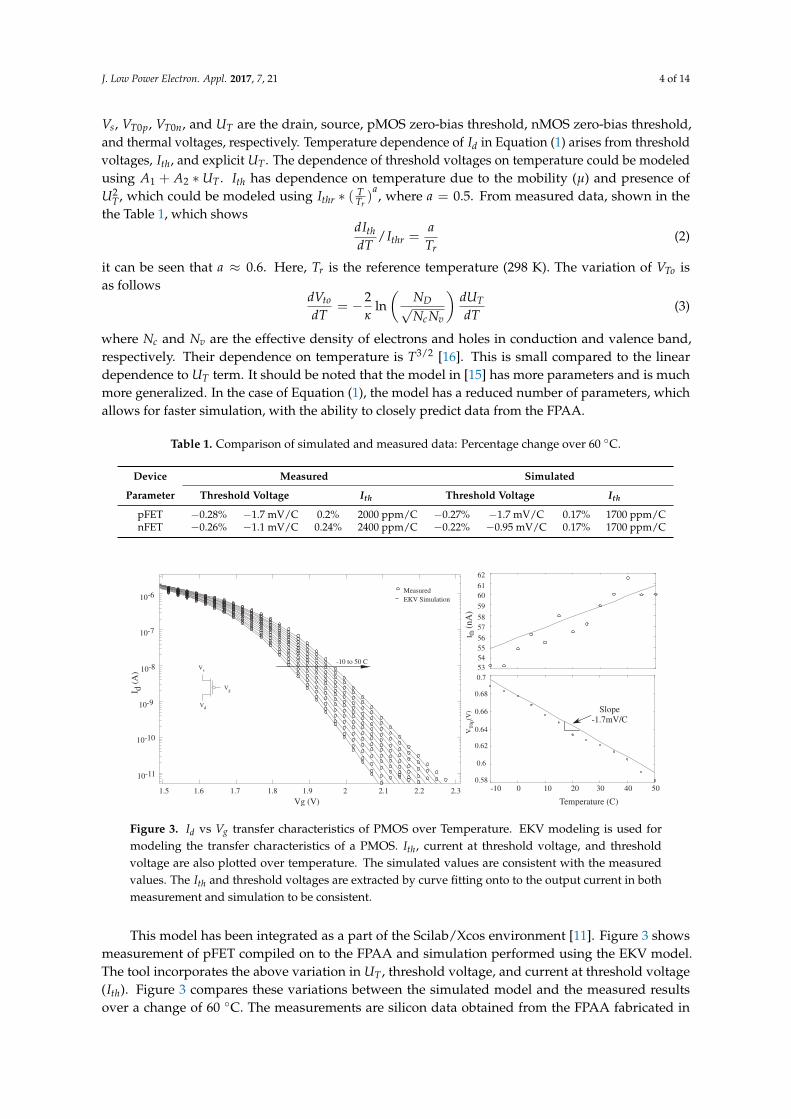
Evaluating the relationship of Iout and Iin over temperature of a current mirror built with a FGpFET, such as the one used in Figure 7 for biasing and shown in the Figure 8, is given by Equation (6).
Iout = Iineκ(V1−V2)/UT (6)
if V1 and V2 in the above equation are equal then we have Iout = Iin. In general, for a non FG currentmirror there is a threshold voltage mismatch between the transistors that will lead to a variation of Iout
with temperature. The variation of current in this case could be modeled as
Iout = Iin A = Iin AT0/T0 where A = eκ(V1−V2)/UT (7)
where T0 is a reference temperature which could be room temperature for simplicity. This effect isimportant in case of a Vector Matrix Multiplication (VMM) , discussed in Section 6, where multiple FGpFETs are biased as a current mirror.
VDDVDD
Iin Iout
V1 V2
Figure 8. A simple FG pFET based current mirror. The mismatch between the two transistor causes Iout
to be not equal to Iin. This also results in temperature dependence of Iout assuming Iin is kept constant.
5.2. FG-Based Voltage Reference without Resistors
The main drawback of the reference circuits introduced in the previous section is the need foran external resistor for different biasing current. There are several resistorless bias reference circuitsthat take advantage of the availability of different Vtnmos or Vtpmos devices, i.e., high and low thresholddevices [23,24]. The aforementioned techniques require an ASIC and availability of different thresholddevices in the process.
Here we propose to use FG to create a difference in threshold voltage by inducing charge at thefloating node. This allows the bias of the reference with a different biasing value and to be able todirectly compile the circuit onto the FPAA. Figure 9 shows the schematics of the proposed referencecircuits. Figure 9a introduces a voltage reference circuit using a FGOTA. VREF is generated by creatingan offset between positive and negative terminals of the FGOTA. A 4VREF of 2.5 mV, with respectto VREF at 25 ◦C, was observed over a range of 60 ◦C. The range of voltage reference that could begenerated with this reference is between 0.346 V to 2.44 V and is plotted in the Figure 9a. It shouldbe noted that VREF is constrained near the GND by the output buffer used for the measurement andis not due to the linear range of the FGOTA. Here, IREF is the programming current and thereforean indicator of the charge programmed onto the FG, which is varied to tune the VREF. For themeasurements in Figure 9a, the FGOTA was biased at 2 µA, and hence the power dissipated by thecircuit is 5 µW. This could change depending on the application, i.e., the load of the reference, and thepower requirements. Considering the above linear range of the FGOTA based voltage reference, it hasa temperature variation of 19.83 ppm/◦C.

J. Low Power Electron. Appl. 2017, 7, 21 9 of 14
VDD
GND
GND
VREF
9.7 mV
-10 0 10 20 30 40 50-6
-5
-4
-3
-2
-1
0
1
2
3
4
Linear Fit
Temperature (C)
∆V
RE
F (
mV
)
b)
-1.5
-1.0
-0.5
0.0
0.5
1.0
1.5
2.0
2.5 mV
10-11 10-10 10-9 10-8 10-7 10-6 10-51.6
1.7
1.8
1.9
2.0
2.1
2.2
VDD
GND
GND
VREF
IREF
IREF (A)
0.0
0.5
1.0
1.5
2.0
2.5
VREF I1 I2
I1 = 500 nA
I2 = IREF
VREF
VREF
∆V
RE
F (
mV
)
a)
GND VREF
Vo
ltag
e (V
)V
olt
age
(V)
Figure 9. Programmable voltage reference without resistors. (a) The figure on the top shows resultsfrom a voltage reference designed using FGOTA connected in a follower configuration. VREF isgenerated by creating an offset between the positive and negative terminals of the FGOTA. A variationof 2.5 mV was observed in the reference voltage value over a change of 60 ◦C. The referencehas a programmable range of 0.346 V to 2.441 V and this is shown in the second part of thefigure; (b) A programmable voltage reference designed using a diode connected pFET and a FG pFETfrom the routing infrastructure. A variation of 9.7 mV was observed for a change of 60 ◦C. The range ofthis reference is 1.66 V to 2.19 V.
Figure 9b shows a voltage reference built using two devices. The FG transistor used in the circuitis part of the routing fabric in the FPAA whereas the pMOS transistor is part of the CAB. A variationof 9.7 mV over 60 ◦C was observed in case of this voltage reference with programming range of 1.66 Vto 2.19 V. Considering this linear range, the reference has a temperature variability of 305 ppm/◦C.The dependence of VREF, in the case of Figure 9b, can be analyzed by reducing the EKV equationin Equation (1). As seen in Equation (8), VREF has a weak dependence on UT and supply voltage VDD.In the following derivation, it is assumed that the κ of the FG pMOS and the diode connected pMOS issimilar and that their σ ≈ 0.
Ithpmose(κ(VDD−VREF−VT0p)/UT = Ith f gpmose(κ(VDD−Vf g−VT0p)−(VDD−VREF))/UT
UT ln(Ithpmos
Ith f gpmos) = κ(VREF −Vf g)− (VDD −VREF)
VREF = UTκ+1 ln(
IthpmosIth f gpmos
) + ( κκ+1 )Vf g + (VDD
κ+1 )
(8)
It should be noted from the above equation that if the Ith of two devices are equal, the outputVREF would be almost invariant over temperature. In addition, the above analysis holds only if thetransistors, the FG transistor, and the pMOS are in the subthreshold saturation regime. Also, the twotransistor circuit would have fairly significant power coupling as opposed to the FGOTA whose PSRRwill be high.
6. Vector Matrix Multiplication (VMM)
A FG based Vector Matrix Multiplication (VMM) is one of the building blocks in an analogclassifier [25,26]. It stores the weight of the classifier as a charge (Q) on the floating node of the FG

J. Low Power Electron. Appl. 2017, 7, 21 10 of 14
pFET. The output of a VMM is a current signal, which is a product of input voltage and the weightstored on the floating node. The equation in Equation (1) can be modified as follows:
Id = Ithe(κ f gpmos(Vdd−Vf g−VT0p)/
UT e−(Vdd−Vin)/UT
Id = Ithe(κ f gpmos(Vdd−Vf gre f−VT0p))/UT We−(Vdd−Vin)/UT
W = e(
κ f gpmos(−∆V′f g))
/UT
(9)
The above set of equations reveals the dependence of weight on temperature. Also, the Vin
would have a different relationship with the output Id with change in temperature given by e−(Vdd−Vin)
UT .Thus the classifier, instead of having an output y = W ′ ∗ x, will have a temperature dependent term.
To demonstrate the dependence of the VMM on temperature, when biased with a DAC, a 12× 1(i.e., a 12 input and 1 output) VMM is compiled on the FPAA. As shown in Figure 10, a shift register isused to measure each FG output over 60 ◦C. A variation of 158 nA is observed when they are nominallybiased around 50 nA at room temperature. This variation could lead to substantial errors while usingthe VMM in classification as temperature could vary depending on the application. As an example,when the classifier is used for classifying an acoustic signal from the knee joint [12], the systemtemperature is expected to change with the environment temperature (e.g., room temperature duringactivities performed at home or to hot/cold temperatures during outdoor activities). To addressthe issue, the current reference introduced in the Section 5.1 is used to bias the FG pMOS of theVMM. Figure 10 shows the variation of the VMM current when biased using the FG current reference.A maximum variation of 5.6 nA is observed in the current. This variation is due to the fact that there isa mismatch in the threshold voltage of the transistor resulting in A0 6= 1, where A0 is the gain factorfrom Equation (7).
VDAC V
DACV
DACV
DAC
Shift RegisterClkDataVDD
EN
Id
45
50
55
Id (
nA
)
20
40
60
80
100
120
140
160
180
Id (
nA
)
1 32 4 5 6 7 8 9 10 11 12
60
VMM Number
0
Shift RegisterClkDataVDD
EN
VREF V
REFV
REFV
REF
Id
Variation = 5.6 nA
Variation = 158 nA50
-10
-10
50
Figure 10. A typical implementation of a Vector Matrix Multiplication, shown here with a shiftregister for measurement, in a FG-based FPAA. The two measurements corresponds to two differentexperimental setups. one where a DAC is used to bias the FG whereas the other corresponds to a FGbiased using the voltage reference discussed earlier. A current variation of 158 nA was observed over60 ◦C when the VMM, programmed to get 50 nA at room temperature, was biased using a DAC.A variation of 5.6 nA was observed in case of the VMM biased using the voltage reference.
The VMM weight is updated depending on the learning of the classifier and hence in practicethe weight will have a certain4Vf g compared to the biasing circuit. This will result in a gain A0 6= 1,thereby leading to dependence of Iout on temperature. If the output stage of the VMM is a Winner TakeAll (WTA) [27], which is the case in [3,12,25], the small variation would not affect the output of the

J. Low Power Electron. Appl. 2017, 7, 21 11 of 14
classifier. This is due to the fact that a WTA compares relative current between the competing branchesof VMM.
7. Variation of Band-Pass Filter
A Gm − C based second order band-pass filter is used extensively for several signal processingsystems [3,4,12]. A second order Gm − C filter enables extracting frequency based features from theinput signal with a low power consumption. Also, a FG based Gm − C offers programmability overbroad range of center frequencies by changing the bias of the FGOTAs. The input of the FGOTA iscapacitively coupled to increase the linearity of the filter. The PSRR, CMRR, input referred noise,and other characteristics of the filter are described in detail here [28].
The inset in Figure 11 shows the schematic of a Gm−C filter compiled in a single CAB of the FPAA.The FGOTA are biased using a FG pFET as seen in Figure 11. Figure 11 shows the frequency response ofthe band-pass filter over 60 ◦C of temperature change when biased using a DAC. Figure 11 also showsa variation in the center frequency, quality factor, and gain of the band-pass filter. The variation in centerfrequency is 2 KHz for a center frequency of 840 Hz at room temperature. This variation would lead tosignificant error in the processing and extraction of features in different signal processing systems.
VDAC
VDD
VDC
VIN
VDAC
VDD
-40
-30
-20
-10
0
10
20
10 100 1000
Frequency (Hz)
Gai
n(d
B)
-50
1.8
2
2.2
11.5
12
12.5
13
13.5
14
Variation 2 dB
Qu
alit
y
Fac
tor
C
ente
r
Fre
qu
ency
(KH
z)G
ain
(dB
)
-10 -5 0 20 305 10 15 25 35 40 45 50
Temperature (C)
1.6
1.4
1.2
1.0
0.8
0.6
00.20.40.60.81
1.21.41.61.82
Variation 2KHz
Variation 1.4
Figure 11. Measured frequency response of second order band-pass Gm − C filter over temperature.A FG pFET is used as a biasing transistor for the OTA. Here, the gate of FG pFET is biased using aDAC as seen in the inset of the frequency response graph. A variation of 2 Khz was observed in centerfrequency of the filter. A variation of 2 dB in gain and 1.4 in the quality factor of the filter was observed.
A FG based current reference generator introduced in the Section 5.1 would be suitable for biasingthe Gm − C filters. Figure 12 shows the bootstrap reference compiled along with the band pass filter.Figure 12 also shows the frequency response of the band-pass filter over a temperature variationof 60 ◦C. The Propotional To Absolute Temperature (PTAT) response of the FG based bootstrapreference helps in compensating the Complementary To Absolute Temperature (CTAT) variation in VT .Figure 12 also shows the variation in the characteristics of the bandpass filter namely quality factor (Q),center frequency (FC), and gain at the center frequency. As compared to the case where it was biasedby a DAC, the variation in center frequency is reduced to 76 Hz, gain variation is 1 dB as opposed to2 dB, and quality factor variation is 0.48 compared to 1.4. Measurements in the Figures 11 and 12 wereperformed consecutively where the filter were biased first with a DAC and then with a FG currentreference to keep other variations constant. The resulting temperature dependent variation of 76 Hz,observed in Figure 12, could be explained due to the fabrication related device-mismatch between theFG pMOS used in the reference circuit and the FG pMOS used as the biasing transistor of the FGOTAsin the bandpass filter. In addition, there are design-related mismatches in the aforementioned FG

J. Low Power Electron. Appl. 2017, 7, 21 12 of 14
pMOS devices as well. For instance, the coupling capacitor of the FG pMOS in the reference circuit is8 fF as opposed to 43 fF incase of the FGOTA biasing device. The other source of mismatch is also dueto different W
L of the FG pMOS transistors, which is 1.8µm600 nm in the case of the FG reference circuit and
6µm2µm . In subsequent designs of the FPAA, these variations will be reduced by keeping a single size ofFG transistors for all the devices on the SoC.
VREF
VDD
VREF
VDD
VDC
VIN
-40
-30
-20
-10
0
10
20
10 100 10000.9
1
1.1
1.2
1.3
1.4
1.5
290
370
300
310
320
330
340
350
360
13
13.2
13.4
13.6
13.8
14
14.2
Qu
alit
y
Fac
tor
C
ente
r
Fre
qu
ency
(Hz)
Gai
n(d
B)
-10 -5 0 20 305 10 15 25 35 40 45 50
Temperature (C)Frequency (Hz)
Variation 76 Hz
Variation 0.48
Variation 1 dB
Gai
n(d
B)
Figure 12. Measured frequency response of second order band-pass Gm − C filter over temperature.Here, the gate of the FG pFET is biased using the FG based voltage reference. A variation of 76 Hz wasobserved in case of the center frequency. A variation of 0.48 in quality factor and 1 dB in gain, at thecenter frequency, of the filter was observed.
8. Summary and Discussion
There has been a growing interest in using FPAA for rapid prototyping of mixed signalsystems, performing mixed and analog signal processing for wide ranging applications, and usingprogrammability and reconfigurability to increase system performance and energy efficiency [5,29–31].Hence, it becomes more important to study the effects of temperature on a reconfigurable platformand investigate methods that could reduce these variations. A FG temperature compensation structureas part of the CAB is used to reduce the variation in current over temperature [32]. This work presentsseveral circuits, models, and techniques to estimate and reduce the temperature variation of sucha system.
The simulation performed using the model developed based on the EKV models were in closeagreement with the measured data. These models created for simple nFET and pFET devices werethen used to study the temperature behavior of simple single ended circuits and were compared withmeasurement results. The intuition created here led to building and designing several of the currentand voltage references introduced in subsequent sections. The references developed in this workare a part of the Scilab/Xcos environment as a block thereby enabling easy compilation as part ofa larger system.
A bootstrap current reference is introduced to bias FG devices on the FPAA. The performanceof the bootstrap reference is studied over temperature and the measured results from the FPAA arepresented. The FG reference circuit is also used to bias two critical components of analog signalprocessing chain, namely the VMM and the second order bandpass filer. Their performance overtemperature when biased using a DAC and the FG reference circuit is studied. A variation of 156 nAwas observed in the output current of the VMM when biased with a DAC as opposed to a variation of5.6 nA, when biased with FG current reference circuit. The bandpass filter’s center frequency varies by2 KHz when biased with a DAC whereas in case of FG reference circuit it varies by 76 Hz.

J. Low Power Electron. Appl. 2017, 7, 21 13 of 14
The work also presents two resistorless voltage references with wide range of programmablevoltages. The FGOTA based voltage reference has a temperature variability of 19.83 ppm/◦Cwhereas the two transistor based voltage reference achieves a precision of 305 ppm/◦C. FGOTAcould also be used as an error amplifier in an LDO without having to generate a separate referencevoltage [33]. All measurements were performed on the FPAA, which is powered using a microUSB.PSRR measurements were not performed since body of all pFET devices are connected to the fixedmicroUSB supply, thus preventing accurate PSRR measurements.
FG devices would requires a programming infrastructure, an overhead in terms of area and power,and would be infeasible as a stand-alone structure. However, in case of an FPAA there are more thenhalf a million FG devices and thus would make it feasible to have a single programming infrastructure.Additionally, using FG devices as routing switches allows for a lower power consumption comparedto an FPGA where dedicated SRAM is required to store the design.
Author Contributions: Sahil Shah, Hakan Toreyin and Jennifer Hasler conceived and designed the experiments;Sahil Shah performed the experiments; Sahil Shah and Jennifer Hasler analyzed the data; Sahil Shah andAishwarya Natarajan developed the transistor models to predict the behaviour of the device over temperature;Sahil Shah and Hakan Toreyin wrote the paper.
Conflicts of Interest: The authors declare no conflict of interest.
References
1. Hersek, S.; Toreyin, H.; Inan, O.T. A Robust System for Longitudinal Knee Joint Edema and Blood FlowAssessment Based on Vector Bioimpedance Measurements. IEEE Trans. Biomed. Circuits Syst. 2016, 10, 545–555.
2. Toreyin, H.; Shah, S.; Hersek, S.; Inan, O.T.; Hasler, J. Proof-of-Concept Energy-Efficient and Real-TimeHemodynamic Feature Extraction from Bioimpedance Signals using a Mixed-Signal Field ProgrammableAnalog Array. In Proceedings of the International Conference on Biomedical and Health Informatics (BHI),Orlando, FL, USA, 16–19 Feburary 2017.
3. Shah, S.; Toreyin, H.; Inan, O.T.; Hasler, J. Reconfigurable Analog Classifier For Knee-Joint Rehabilitation.IEEE Eng. Med. Biol. Soci. 2016, doi:10.1109/EMBC.2016.7591797.
4. Sahil, S.; Jennifer, H. Low Power Speech Detector On A FPAA. Presented at ISCAS 2017, Baltimore, MD,USA, 28–31 May 2017.
5. George, S.; Kim, S.; Shah, S.; Hasler, J.; Collins, M.; Adil, F.; Wunderlich, R.; Nease, S.; Ramakrishnan, S.A Programmable and Configurable Mixed-Mode FPAA SoC. IEEE Trans. Very Large Scale Integr. (VLSI) Syst.2016, 24, 2253–2261.
6. Teague, C.; Hersek, S.; Toreyin, H.; Millard-Stafford, M.L.; Jones, M.L.; Kogler, G.F.; Sawka, M.N.; Inan, O.T.Novel approaches to measure acoustic emissions as biomarkers for joint health assessment. In Proceedingsof the 2015 IEEE 12th International Conference on Wearable and Implantable Body Sensor Networks (BSN),Cambridge, MA, USA, 9–12 June 2015; pp. 1–6.
7. Etemadi, M.; Inan, O.T.; Heller, J.A.; Hersek, S.; Klein, L.; Roy, S. A Wearable Patch to Enable Long-TermMonitoring of Environmental, Activity and Hemodynamics Variables. IEEE Trans. Biomed. Circuits Syst.2016, 10, 280–288.
8. Shah, S.; Smith, J.; Stowell, J.; Christen, J.B. Biosensing platform on a flexible substrate. Sens. ActuatorsB Chem. 2015, 210, 197–203.
9. Ahuja, B.K.; Vu, H.; Laber, C.A.; Owen, W.H. A very high precision 500-nA CMOS floating-gate analogvoltage reference. IEEE J. Solid-State Circuits 2005, 40, 2364–2372.
10. Kim, S.; Shah, S.; Wunderlich, R.; George, S.; Hasler, J. CAD Synthesis Tools for Large-Scale Floating-GateFPAA System. Trans. Comput. Aided Des. 2017, under review.
11. Natarajan, A.; Hasler, J. Modeling, simulation and implementation of circuit elements in an open-source toolset on the FPAA. Anal. Integr. Circuits Signal Process. 2017, 91, 119–130.
12. Shah, S.; Teague, C.N.; Inan, O.T.; Hasler, J. A Proof-of-Concept Classifier for Acoustic Signals from the KneeJoint on a FPAA. In Proceedings of the 2016 IEEE SENSORS, Orlando, FL, USA, 30 Octorber–3 November 2016.
13. Gurun, G.; Tekes, C.; Zahorian, J.; Xu, T.; Satir, S.; Karaman, M.; Hasler, J.; Degertekin, F.L. Single-chipCMUT-on-CMOS front-end system for real-time volumetric IVUS and ICE imaging. IEEE Trans. Ultrason.Ferroelectr. Freq. Control 2014, 61, 239–250.
J. Low Power Electron. Appl. 2017, 7, 21 14 of 14
14. Kim, S.; Hasler, J.; George, S. Integrated Floating-Gate Programming Environment for System-Level ICs.IEEE Trans. Very Large Scale Integr. (VLSI) Syst. 2016, 24, 2242–2252.
15. Enz, C.C.; Krummenacher, F.; Vittoz, E.A. An analytical MOS transistor model valid in all regions ofoperation and dedicated to low-voltage and low-current applications. Anal. Integr. Circuits Signal Process.1995, 8, 83–114.
16. Pierret, R. Semiconductor Device Fundamentals; Addison-Wesley: Boston, MA, USA, 1996.17. Hasler, J.; Kim, S.; Adil, F. Scaling Floating-Gate Devices Predicting Behavior for Programmable and
Configurable Circuits and Systems. J. Low Power Electron. Appl. 2016, 6, 13.18. Minch, B. EKV MOS Transistor Model Summary. Available online: http://madvlsi.olin.edu/circuits/
handouts.html (accessed on 2 Feburary 2017).19. Degnan, B.P. Temperature Robust Programmable Subthreshold Circuits Through A Balanced Force Approach.
Ph.D. Thesis, Georgia Institute of Technology, Atlanta, GA, USA, 2013.20. Kim, S.; Shah, S.; Hasler, J. Calibration of Floating-Gate SoC FPAA System. IEEE Trans. Very Large Scale Integr.
(VLSI) Syst. 2017, 25, 2649–2657.21. Vittoz, E.; Fellrath, J. CMOS analog integrated circuits based on weak inversion operations. IEEE J. Solid-State
Circuits 1977, 12, 224–231.22. Srinivasan, V.; Serrano, G.; Twigg, C.M.; Hasler, P. A Floating-Gate-Based Programmable CMOS Reference.
IEEE Trans. Circuits Syst. I Regul. Pap. 2008, 55, 3448–3456.23. Georgiou, J.; Toumazou, C. A resistorless low current reference circuit for implantable devices.
In Proceedings of the 2002 IEEE International Symposium on Circuits and Systems (Cat. No. 02CH37353),Phoenix-Scottsdale, AZ, USA, 26–29 May 2002; Volume 3, pp. III-193–III-196.
24. Seok, M.; Kim, G.; Blaauw, D.; Sylvester, D. A Portable 2-Transistor Picowatt Temperature-CompensatedVoltage Reference Operating at 0.5 V. IEEE J. Solid-State Circuits 2012, 47, 2534–2545.
25. Ramakrishnan, S.; Hasler, J. Vector-Matrix Multiply and Winner-Take-All as an Analog Classifier.IEEE Trans. Very Large Scale Integr. (VLSI) Syst. 2014, 22, 353–361.
26. Ramakrishnan, S.; Basu, A.; Chiu, L.K.; Hasler, J.; Anderson, D.; Brink, S. Speech Processing ona Reconfigurable Analog Platform. IEEE Trans. Very Large Scale Integr. (VLSI) Syst. 2014, 22, 430–433.
27. Lazzaro, J.; Ryckebusch, S.; Mahowald, M.; Mead, C.A. Winner-Take-All Networks of O(N) Complexity.In Advances in Neural Information Processing Systems 1; Touretzky, D., Ed.; Morgan-Kaufmann: Burlington,MA, USA, 1989; pp. 703–711.
28. Graham, D.W.; Hasler, P.E.; Chawla, R.; Smith, P.D. A Low-Power Programmable Bandpass Filter Section forHigher Order Filter Applications. IEEE Trans. Circuits Syst. I Regul. Pap. 2007, 54, 1165–1176.
29. Guo, N.; Huang, Y.; Mai, T.; Patil, S.; Cao, C.; Seok, M.; Sethumadhavan, S.; Tsividis, Y. Energy-EfficientHybrid Analog/Digital Approximate Computation in Continuous Time. IEEE J. Solid-State Circuits 2016,51, 1514–1524.
30. Dorigo, D.D.; Manoli, Y. An OTA-C signal processing FPAA with 305 MHz GBW and integratedfrequency-independent filter tuning. In Proceedings of the 2016 IEEE Asian Solid-State Circuits Conference(A-SSCC), Toyama, Japan, 7–9 November 2016; pp. 61–64.
31. Becker, J.; Anders, J.; Ortmanns, M. A continuous-time field programmable analog array with 1 GHz GBW.In Proceedings of the 2016 IEEE International Conference on Electronics, Circuits and Systems (ICECS),Monte Carlo, Monaco, 11–14 December 2016; pp. 209–212.
32. Dilello, A.; Andryzcik, S.; Kelly, B.M.; Rumberg, B.; Graham, D.W. Temperature Compensation ofFloating-Gate Transistors in Field-Programmable Analog Arrays. In Proceedings of the IEEE InternationSymposium on Circuits and System, Baltimore, MD, USA, 28 May 2017.
33. Peng, S.Y.; Liu, L.H.; Chang, P.K.; Wang, T.Y.; Li, H.Y. A Power-Efficient Reconfigurable Output-Capacitor-LessLow-Drop-Out Regulator for Low-Power Analog Sensing Front-End. IEEE Trans. Circuits Syst. I Regul. Pap.2017, 64, 1318–1327.
c© 2017 by the authors. Licensee MDPI, Basel, Switzerland. This article is an open accessarticle distributed under the terms and conditions of the Creative Commons Attribution(CC BY) license (http://creativecommons.org/licenses/by/4.0/).