Embed Size (px)
Citation preview

Modern VLSI Design 3e: Chapter 5,6 Copyright 2002 Prentice Hall PTR Adapted by Yunsi Fei
Topics
Sequential machine (§5.2, §5.3)
FSM construction (§5.4)
Testing and design for testability (§4.8, §5.7)– Fault models– Combinational logic testing– Sequential logic testing

Modern VLSI Design 3e: Chapter 5,6 Copyright 2002 Prentice Hall PTR Adapted by Yunsi Fei
Manufacturing Testing
Errors are introduced during manufacturing Testing: manufacturing validation Varieties of testing:
– functional testing– performance testing (binning chips by speed)
Testing also weeds out infant mortality

Modern VLSI Design 3e: Chapter 5,6 Copyright 2002 Prentice Hall PTR Adapted by Yunsi Fei
Fault Modeling
Fault model– Convert a physical problem to a logical problem– Stuck-at, stuck-open, delay ... fault models– Single-fault assumption
With fault models+ Simulate the I/O behavior produced by the fault + Find possible locations of faults– impossible to incorporate all manufacturing faults
» Can’t guarantee the circuit is fault-free even if no fault is found under the fault model

Modern VLSI Design 3e: Chapter 5,6 Copyright 2002 Prentice Hall PTR Adapted by Yunsi Fei
Stuck-at-0/1 Faults
Stuck-at-0/1 (s-a-0/1): a wire is always stuck at 0 or 1, independent of its drive value– Easiest and useful in practice, thus most popular
10B
A
C
01B
A
C
01B
A
C
10B
A
C

Modern VLSI Design 3e: Chapter 5,6 Copyright 2002 Prentice Hall PTR Adapted by Yunsi Fei
Stuck-at-open/closed Model
Models transistors always on/off– how do we test t1
stuck-open?

Modern VLSI Design 3e: Chapter 5,6 Copyright 2002 Prentice Hall PTR Adapted by Yunsi Fei
Delay Fault
Delay falls outside acceptable limits– gate delay fault model:
» assume that all delays are lumped into one gate;
– path delay fault models:» assume delay problems along path through network.
Delay problems reduce yield– performance problems;– functional problems in some types of circuits.
Modern VLSI Design 3e: Chapter 5,6 Copyright 2002 Prentice Hall PTR Adapted by Yunsi Fei
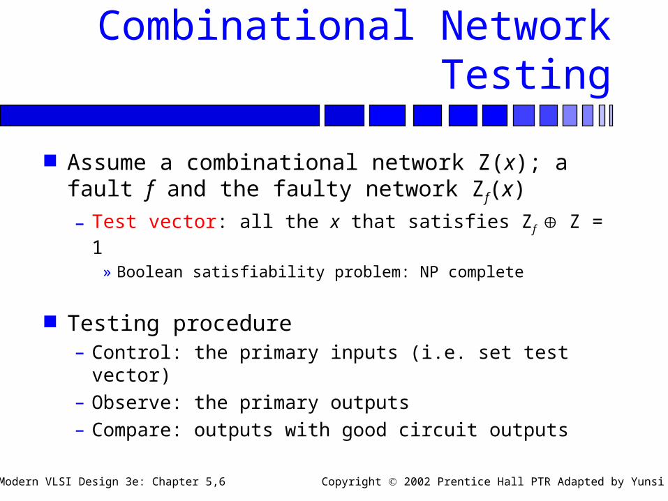
Combinational Network Testing
Assume a combinational network Z(x); a fault f and the faulty network Zf(x)
– Test vector: all the x that satisfies Zf Z = 1» Boolean satisfiability problem: NP complete
Testing procedure– Control: the primary inputs (i.e. set test vector)
– Observe: the primary outputs
– Compare: outputs with good circuit outputs

Modern VLSI Design 3e: Chapter 5,6 Copyright 2002 Prentice Hall PTR Adapted by Yunsi Fei
Combinational Testing Example
1
Goal: test output of gate D for s-a-0 fault
A
B
C
D
E
F
0i1
i2
i3i4
i5
i6
O
s-a-0
0
1
0

Modern VLSI Design 3e: Chapter 5,6 Copyright 2002 Prentice Hall PTR Adapted by Yunsi Fei
Testing Procedure
Two major steps:– Propagate (forward):
» set the internal lines so that the faulty value can be seen at the PO
– Justify (backward)» set the PIs so that the internal lines can be justified
Reconvergent fanouts– make justification difficult

Modern VLSI Design 3e: Chapter 5,6 Copyright 2002 Prentice Hall PTR Adapted by Yunsi Fei
Redundancy
If Zf Z, there is no way to find the fault
– Can’t justify
Redundancy causes Zf Z
– Z(x) = a + ab (s-a-1 for the a in ab)– Hard to completely remove redundancy
ab
Z
s-a-1
Modern VLSI Design 3e: Chapter 5,6 Copyright 2002 Prentice Hall PTR Adapted by Yunsi Fei
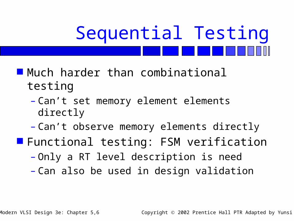
Sequential Testing
Much harder than combinational testing– Can’t set memory element elements directly– Can’t observe memory elements directly
Functional testing: FSM verification– Only a RT level description is need– Can also be used in design validation

Modern VLSI Design 3e: Chapter 5,6 Copyright 2002 Prentice Hall PTR Adapted by Yunsi Fei
FSM Verification
Given a sequential circuit S, how do we verify it actually is the FSM we want?– Initialization: bring S to a known state
» E.g. “0” initializes the sequencer to state S0
– Verify S has (at least) n states» Given k flip-flops, can know S has at most 2k states
» If n = 2k, can then verify S has n states
– Verify every transition in the state table of S

Modern VLSI Design 3e: Chapter 5,6 Copyright 2002 Prentice Hall PTR Adapted by Yunsi Fei
Sequence Recognizer Example
Present input next outputS0 (00) 0 S0 (00) 00S0 (00) 1 S1 (01) 00S1 (01) 0 S0 (00) 01S1 (01) 1 S2 (10) 00S2 (10) 0 S0 (00) 11S2 (10) 1 S2 (10) 00
0--
A
000
A
100
B
001
A
100
B
100
C
011
A
000
A
100
C
000
A
000
A

Modern VLSI Design 3e: Chapter 5,6 Copyright 2002 Prentice Hall PTR Adapted by Yunsi Fei
Time-frame Expansion
Another way to look at FSM verification– Unroll machine in time
– One SA fault becomes multiple faults

Modern VLSI Design 3e: Chapter 5,6 Copyright 2002 Prentice Hall PTR Adapted by Yunsi Fei
Unreachable States
State assignment may cause some states to be unreachable– E.g. “11” in the sequence recognizer
FSM verification– Violate the maximum states assumption
» E.g. The sequence recognizer would not tell the difference between a 1110/10 sequence recognizer
Time-frame expansion– Unable to set an internal value
Modern VLSI Design 3e: Chapter 5,6 Copyright 2002 Prentice Hall PTR Adapted by Yunsi Fei
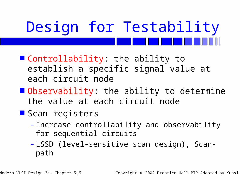
Design for Testability
Controllability: the ability to establish a specific signal value at each circuit node
Observability: the ability to determine the value at each circuit node
Scan registers– Increase controllability and observability for
sequential circuits– LSSD (level-sensitive scan design), Scan-path

Modern VLSI Design 3e: Chapter 5,6 Copyright 2002 Prentice Hall PTR Adapted by Yunsi Fei
Full Scan Method
Connect all the system flip-flops in a scan chain as a big shift register
When in “test” mode– Stop system clock– Scan in the value for each flip-flop in the chain – Run the system clock for one or more cycles– Scan out the value for each flip-flop in the chain

Modern VLSI Design 3e: Chapter 5,6 Copyright 2002 Prentice Hall PTR Adapted by Yunsi Fei
Scan Chain
Scan-in
Scan-out

Modern VLSI Design 3e: Chapter 5,6 Copyright 2002 Prentice Hall PTR Adapted by Yunsi Fei
An LSSD Latch
D1
CK1
CK2
CK3
D2
Q

Modern VLSI Design 3e: Chapter 5,6 Copyright 2002 Prentice Hall PTR Adapted by Yunsi Fei
A Multiplexed D Flip-flop
D Q
TE
D Q
D2
D1
Q

Modern VLSI Design 3e: Chapter 5,6 Copyright 2002 Prentice Hall PTR Adapted by Yunsi Fei
Partial Scan
Full scan is expensive—must roll out and roll in state many times during a set of tests.
Partial scan selects some registers for scannability.
Requires analysis to choose which registers are best for scan.

Modern VLSI Design 3e: Chapter 5,6 Copyright 2002 Prentice Hall PTR Adapted by Yunsi Fei
Boundary Scan
Board-level debugging
scan_in
scan_out