Embed Size (px)
Citation preview

Grainger Center for Electric Machinery and Electromechanics Department of Electrical and Computer Engineering
University of Illinois at Urbana-Champaign 1406 W. Green St. Urbana, IL 61801
The information contained in this Document and the Appendices may not be copied, reproduced, distributed or stored in a retrieval system without the prior express written permission of the author.
Copyright 2003 by the Board of Trustees of the University of Illinois. All Rights Reserved
Specification Document
Modular Inverter System Specification
Reference: SD00004
Issue: 002
Status: Issued
Author: Jonathan Kimball
Principal Investigator: P.T. Krein
Created: September 9, 2003
\\ece-powernts2\ece power design archives\documents\specification documents\sd00004-001 modular inverter system specification.doc
Abstract:
This document provides an overview of the modular inverter design project, as well as specifying
interconnects where applicable. It is not intended to be comprehensive, but it does specify
necessary functionality.
Modular Inverter System Specification Specification Document Issue 002 SD00004
Modular Inverter System Specification Status: Work in Progress Page 2 of 11 Printed 11/24/2010: 10:40 AM
Copyright 2003 University of Illinois
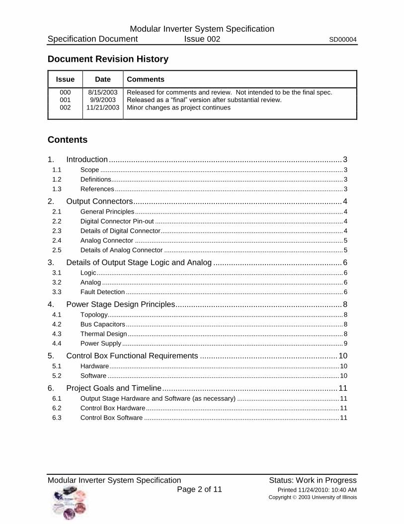
Document Revision History
Issue Date Comments
000 8/15/2003 Released for comments and review. Not intended to be the final spec. 001 9/9/2003 Released as a “final” version after substantial review. 002 11/21/2003 Minor changes as project continues
Contents
1. Introduction ......................................................................................................... 3
1.1 Scope ..................................................................................................................................... 3
1.2 Definitions............................................................................................................................... 3
1.3 References ............................................................................................................................. 3
2. Output Connectors .............................................................................................. 4
2.1 General Principles .................................................................................................................. 4
2.2 Digital Connector Pin-out ....................................................................................................... 4
2.3 Details of Digital Connector.................................................................................................... 4
2.4 Analog Connector .................................................................................................................. 5
2.5 Details of Analog Connector .................................................................................................. 5
3. Details of Output Stage Logic and Analog .......................................................... 6
3.1 Logic ....................................................................................................................................... 6
3.2 Analog .................................................................................................................................... 6
3.3 Fault Detection ....................................................................................................................... 6
4. Power Stage Design Principles ........................................................................... 8
4.1 Topology................................................................................................................................. 8
4.2 Bus Capacitors ....................................................................................................................... 8
4.3 Thermal Design ...................................................................................................................... 8
4.4 Power Supply ......................................................................................................................... 9
5. Control Box Functional Requirements .............................................................. 10
5.1 Hardware .............................................................................................................................. 10
5.2 Software ............................................................................................................................... 10
6. Project Goals and Timeline ............................................................................... 11
6.1 Output Stage Hardware and Software (as necessary) ........................................................ 11
6.2 Control Box Hardware .......................................................................................................... 11
6.3 Control Box Software ........................................................................................................... 11

Modular Inverter System Specification Specification Document Issue 002 SD00004
Modular Inverter System Specification Status: Work in Progress Page 3 of 11 Printed 11/24/2010: 10:40 AM
Copyright 2003 University of Illinois
1. Introduction
The purpose of the modular inverter project is to provide test beds for future projects. Deliverables
include:
40A, 30VDC inverter stage
20A, 60VDC inverter stage
40A, 400VDC inverter stage (possibly pushed off until the spring semester)
Control box based on a TI 2812 DSP
DSP software to provide interface to a PC
DSP software for V/Hz operation
The desired time frame is to have functional hardware by the end of the fall semester of 2003, with
at least the output stages thoroughly debugged. At least some software should also be done at this
time. The complete software project should be finished by the beginning of fall ’04.
This project is supported by the Grainger Center for Electric Machinery and Electromechanics.
1.1 Scope
The software developed will be primarily limited to minimal functionality such that someone doing
a motor project can get up and running quickly, or someone can develop PC software to implement
an advanced algorithm. Actual vector control algorithms will be implemented by the specific
researcher. It is also desirable to use canned vector control algorithms such that a demo can be
done for ECE333 or ECE468 during spring ’04.
The hardware will be rugged and debugged well enough for the average graduate student to use it.
It does not need to be rugged enough for classroom purposes at this time.
The initial designs are for the standard inverter topology. If possible, it would be nice to be able to
change to an SR (switched reluctance) topology. If the added flexibility degrades the performance
of the standard topology, then the SR topology will be pushed off to a future output stage design.
Initially, three of each unit will be built. Eventually, ten control boxes will be built so that many
researchers can do different things at the same time.
1.2 Definitions
Control box: a box containing the DSP and various interface ports, which generates PWM
commands.
Output stage: a box containing four halfbridges, interface to the control box, some logic, and gate
drivers.
Power stage: subsystem of the output stage consisting of only the power handling devices.
Output connector: the connector between the control box and the output stage. Actually two
connectors, one analog, one digital.
1.3 References

Modular Inverter System Specification Specification Document Issue 002 SD00004
Modular Inverter System Specification Status: Work in Progress Page 4 of 11 Printed 11/24/2010: 10:40 AM
Copyright 2003 University of Illinois
2. Output Connectors
2.1 General Principles
The digital signals are transmitted as RS-422 differential pairs. The output stage should include
pull-up and pull-down resistors such that when the connector is unplugged, the power stage is
open-circuited.
The analog signals use a maximum range of ±10V. A Kelvin analog grounds (one or more) are
included. The control box should treat all signals as differential with respect to the Kelvin.
There are two connectors, one analog and one digital. Both are ribbon cables. Latching headers
are preferred. For the digital connector, use Vari-Twist cable, which pairs adjacent conductors.
For the analog connector, consider using shielded ribbon cable if a suitable type can be found.
All of the “GND” connections are tied together at both ends of the cable. Within each box, it is
recommended to separate digital, analog, and power grounds between the cable and the rest of the
circuitry. “GND” is connected to earth via a resistor and a capacitor in parallel (relatively low
impedance).
The power supplies on the connectors are intended to power analog and digital circuitry in the
control box. They originate in the output stage. Current requirements are TBD.
It is assumed that the bus supply to the power stage is at a very different potential than earth. Full
isolation is required between the output connectors and the power stage.
2.2 Digital Connector Pin-out
Pin Signal Pin Signal
1 +5V 18 ~D1
2 GND 19 D2
3 +5V 20 ~D2
4 GND 21 ENABLE
5 A1 22 ~ENABLE
6 ~A1 23 FAULT
7 A2 24 ~FAULT
8 ~A2 25 uC_RESET
9 B1 26 ~uC_RESET
10 ~B1 27 RESERVED
11 B2 28 RESERVED
12 ~B2 29 RESERVED
13 C1 30 RESERVED
14 ~C1 31 RESERVED
15 C2 32 RESERVED
16 ~C2 33 RESERVED
17 D1 34 RESERVED
2.3 Details of Digital Connector

Modular Inverter System Specification Specification Document Issue 002 SD00004
Modular Inverter System Specification Status: Work in Progress Page 5 of 11 Printed 11/24/2010: 10:40 AM
Copyright 2003 University of Illinois
A1 corresponds to the upper device of phase A. A2 corresponds to the lower device of phase A.
\A1 and \A2 are the complements of A1 and A2 respectively for RS-422. It is recommended to use
DS26LS31 transmitters and DS26LS32 receivers, or equivalent or superior devices. These are
quad line drivers and receivers. Remember to terminate the line properly, as well as inserting
proper pull-up and pull-down resistors to bias the signal in the event of an open-circuit.
Similarly, (\)Bn correspond to phase B, (\)Cn correspond to phase C, and (\)Dn correspond to phase
D. Typically, for a three-phase inverter, phases A, B, and C are used as a positive sequence, but
other topologies and other sequences are possible and allowable.
FAULT, ENABLE, and uC_RESET are similar RS-422 signals. When everything is OK, FAULT
and ENABLE should both be high and uC_RESET should be low. FAULT indicates that a fault
has been detected in the output stage. ENABLE is low until the processor is ready to start
providing PWM commands. uC_RESET pulses to clear a fault.
Note that only the first 26 pins are used at this time. A 34-pin connector is used to distinguish it
from the analog connector, as well as providing room for future expansion. Leave the unused pins
floating at this time. Note that it is possible to use 26-conductor Vari-Twist cable at this time,
which is available from ECE Stores.
2.4 Analog Connector
Pin Signal Pin Signal
1 GND 14 KELVIN2
2 +15V 15 RESERVED
3 -15V 16 RESERVED
4 GND 17 RESERVED
5 IA 18 RESERVED
6 IB 19 KELVIN3
7 IC 20 GND
8 ID 21 GND
9 KELVIN1 22 VA
10 VBUS 23 VB
11 T1 24 VC
12 T2 25 VD
13 IBUS 26 KELVIN4
2.5 Details of Analog Connector
IA, IB, IC, and ID correspond to phase currents on phases A, B, C, and D respectively. They are
positive for current going out of the power stage. VA, VB, VC, and VD are phase voltages with
respect to the negative bus, corresponding to phases A, B, C, and D respectively. Vbus is the total
bus voltage. T1 and T2 are relevant temperatures. Scaling is discussed in section 3.
Kelvin ground connections are provided, one for each group of signals. All analog signals should
be treated as differential with respect to the corresponding Kelvin connection. This eliminates
voltage drop and noise in the current-carrying ground wires from influencing the analog
measurements. Note that the groups are in fours, for either quad op amps or two dual op amps per
Kelvin.

Modular Inverter System Specification Specification Document Issue 002 SD00004
Modular Inverter System Specification Status: Work in Progress Page 6 of 11 Printed 11/24/2010: 10:40 AM
Copyright 2003 University of Illinois
3. Details of Output Stage Logic and Analog
3.1 Logic
At a minimum, the logic must prevent simultaneous turn-on of both devices in a halfbridge.
Preferably, minimum deadtime will be enforced. The minimum deadtime must be specified, so that
the software designer can account for it. Typically, the software will insert deadtime greater than
the minimum, so that the output stage logic is transparent.
Faults will be detected as described in section 3.3. On any fault, the logic must latch, turn off all
devices, and signal a fault on the output connector. Faults are reset on power-up, and only on
power-up.
It is also desired to support a minimal command function, where only the upper device commands
are supplied. This will be jumper selectable. The logic must then perform inversion with deadtime
to generate the lower device commands.
3.2 Analog
The phase currents will be detected by closed-loop Hall-effect devices or equivalent. The analog
circuitry will condition these signals, typically a current that is some fixed ratio of the phase
current, into properly scaled voltage signals. Scaling is such that the rated RMS current (e.g. 20A)
corresponds to 4.5V. This allows proper headroom for overload and ripple below the 10V
maximum. The signals are bipolar, positive for outgoing current. It is desirable to include some
means of reducing the scale factor to correspond to a lower rated RMS current, yielding greater
signal amplitude for smaller machines. This can be a resistor change, a jumper, or changing the
number of turns through the sensor.
The bus voltage and phase voltage sensing circuits must be isolated from the main analog circuitry.
The lowest-tech way to perform isolation is through differential amplifiers with large resistors. In
this case, the resistors must be sized so that at maximum voltage rating of the power stage, the
resistor current is less than 5 mA. Take some care in designing the remainder of the circuit,
particularly in choosing an op amp, to account for large resistor values with tolerance. These
signals are mostly unipolar, although phase voltage does extend below the negative bus by at least a
diode drop. These signals should be scaled so that maximum voltage rating corresponds to an 8V
signal, for headroom.
Minimize the filtering on voltage and current signals. The control box is responsible for low-pass
filtering to prevent aliasing of the A/D converter. Since the output stage designer has no control
over the sampling rate, achieve the highest bandwidth possible in the analog signals and let the
control box designer make the filtering decisions.
There is also allowance for up to two temperature feedback signals. These should be scaled so that
0°C = 0 V, 100°C = 5V. The sensors should be placed in relevant positions on e.g. the heat sink.
3.3 Fault Detection
Within the output stage, the following faults should be detected and latched:
Short-circuit. This is sensed via desaturation detection. Even in MOSFET-based designs,
short-circuits can be destructive and require shutdown within 10 s.

Modular Inverter System Specification Specification Document Issue 002 SD00004
Modular Inverter System Specification Status: Work in Progress Page 7 of 11 Printed 11/24/2010: 10:40 AM
Copyright 2003 University of Illinois
Overcurrent. Trip at 9.75V of current feedback. Some filtering is allowable, but shutdown
within 100 s is advised.
Overvoltage. Trip at an appropriate level that will prevent damage to any of the devices in
the system. This should be above the 8V signal level, but perhaps not by much.
When a fault is detected, the priority is to turn off all of the devices. Some gate drivers include soft
turn-off for short-circuit, which is fine. Presumably, before the logic can turn off the rest of the
devices, the gate driver has completed its soft turn-off. The second priority is to alert the control
box via the FAULT signal. The third priority is to indicate the fault in some way, such as an LED
indicator (one for each type of fault for each halfbridge).

Modular Inverter System Specification Specification Document Issue 002 SD00004
Modular Inverter System Specification Status: Work in Progress Page 8 of 11 Printed 11/24/2010: 10:40 AM
Copyright 2003 University of Illinois
4. Power Stage Design Principles
4.1 Topology
The power stage will be composed of four halfbridges. Each halfbridge is composed of two
controlled switches (MOSFETs or IGBTs) with anti-parallel diodes. Although a MOSFET
includes an integral body diode, it is advisable to include a place to insert a Schottky rectifier. This
need may be eliminated by using a MOSFET co-packed with a Schottky, similar to an IGBT/diode
co-pack. Three halfbridges are almost always used; the fourth may be for a brake or to control the
neutral.
It is advisable to include a large diode on the input for reverse-polarity protection. In certain cases,
this diode is not needed, and actually is a hindrance. For these cases, a jumper must be provided to
allow bidirectional current flow. Additionally, there should be a relay that is powered from the
same 120V feed that runs the logic supply. The normally-open contacts should be in series with
the DC supply; the normally-closed contacts should connect a resistor across the bus to bleed down
any capacitive energy.
As previously mentioned, it is desired to include a reconfiguration possibility for an SR topology,
in which the halfbridge is split into two halves. If this compromises the performance of the normal
halfbridge, then SR will be pushed to a future project.
It is necessary to be able to sense many voltages within the system. It is advisable to provide non-
current-carrying binding post connections to every relevant voltage point.
4.2 Bus Capacitors
The input to the power stage is assumed to be well-filtered DC (ripple less than 5%), such as a
Kenwood, HP or MagnaPower supply or an HP programmable load. It is necessary to at least
include a snubber capacitor, a reasonably sized film capacitor close to the IGBTs/MOSFETs. It is
also advisable to include a place to add some bulk capacitance (electrolytic) if that becomes
necessary. A good rule of thumb is to size the bulk capacitance for approximately 6 ms of energy
storage. Inrush control is necessary for the bulk capacitors as well. Note that regeneration will
typically require some bus capacitance in order to maintain stability.
4.3 Thermal Design
Each power stage will have a continuous current rating (e.g. 20A) and a maximum bus voltage
rating (e.g. 60VDC). Thermally, it must be possible to operate at these maxima indefinitely with
junction temperatures below 100°C in lab ambient (25°C). Full rating is at 10 kHz switching for
power stages under 100V, 5 kHz switching for higher voltages.
In addition, the power stage must be capable of overloads up to 125% of the continuous current
rating (e.g. 25A) for 10 s with junction temperatures below 135°C. It is recommended to provide a
derate curve, current vs. overload time, based on the final design, based on a maximum junction
temperature of 135°C. It is anticipated that this will follow a curve of constant (Iactual2 – Irated
2)×tOL,
or possibly some similar form with a different exponent, or possibly two curves to cover the total
range.

Modular Inverter System Specification Specification Document Issue 002 SD00004
Modular Inverter System Specification Status: Work in Progress Page 9 of 11 Printed 11/24/2010: 10:40 AM
Copyright 2003 University of Illinois
Some thought should be given to the removal of the heat from the box. For example, if the heat
sink is entirely contained within the box, the total thermal resistance to ambient includes the
thermal resistance of the box. This can lead to high internal ambient temperatures, inappropriate
for maintaining high-performance analog circuitry.
The ratings chosen are generally larger than what is necessary, “just in case.” Thermally, the
design will probably be overkill for many applications. Consider using a thermostat to control the
fan to reduce noise during low-power operation.
4.4 Power Supply
Each gate driver needs a power supply, possibly bipolar, referenced to the associated emitter/source
connection. Several possibilities exist:
One supply referenced to the negative bus, with bootstrap capacitors to power the upper
devices. Not recommended due to uncertainty of the upper supply voltages.
One supply referenced to the negative bus, with a switcher (forward, flyback) to generate
the upper supplies.
One supply referenced to approximately earth, with a switcher (forward, flyback) to
generate all of the isolated supplies. This same supply can then be used for other “GND”
referenced functions.
In any event, the source supply can be an off-the-shelf supply (of which we have cases). Before
trying the second option, verify the isolation of the supply.

Modular Inverter System Specification Specification Document Issue 002 SD00004
Modular Inverter System Specification Status: Work in Progress Page 10 of 11 Printed 11/24/2010: 10:40 AM
Copyright 2003 University of Illinois
5. Control Box Functional Requirements
5.1 Hardware
The control box must be highly flexible. To that end, it will contain a board with:
Output connectors, which are RS-422 digital and ±10V differential analog
A digital connector that is TTL
An analog connector that is ±10V single-ended
An analog connector that is 0-3V single-ended
A connector for a keypad or similar user interface
An encoder input and an encoder re-transmit
The TTL digital signals will be pass-throughs of the output connector, encoder input, and the
keypad connector for use by a microprocessor, DSP, or PC via a DAQ card. Logic families should
be 3.3V. The single-ended analog connectors will also be essentially pass-throughs, but with
protection against overvoltages and other potentially harmful conditions.
This board will be in a box that has space reserved for a TI 2812 eZdsp board. The box will also
have means to mount a keypad TBD.
Potential systems in this scheme include:
A 2812 eZdsp running V/Hz, vector control, or other advanced control scheme
A PC running xPC derived from a Simulink design
A microcontroller and CPLD running some other control scheme
5.2 Software
It is anticipated that a typical project flow includes a quick design in Simulink followed by a
detailed design in C on a 2812 DSP. To that end, software modules should be designed to assist a
new user:
Simulink subsystems for interfacing to the hardware, including fault and overload
monitoring
DSP subsystems for interfacing to the hardware, including fault and overload monitoring
DSP functions that are generally useful, such as PWM generation, Park-Clarke
transformations, PID loops
DSP interface to the keypad, including parameter storage
Additionally, for people doing motor work, it is desired to have a simple V/Hz algorithm
implemented in the DSP available. It should generate precise sine waves, including dead-time
compensation and other means of attaining high fidelity.
To enable the use of a DAQ card, one seat of Real-Time Workshop and one seat of xPC Target will
be purchased.

Modular Inverter System Specification Specification Document Issue 002 SD00004
Modular Inverter System Specification Status: Work in Progress Page 11 of 11 Printed 11/24/2010: 10:40 AM
Copyright 2003 University of Illinois
6. Project Goals and Timeline
6.1 Output Stage Hardware and Software (as necessary)
Block diagram and preliminary part selection: September 12, 2003
Breadboard prototypes of critical circuits: October 10
Complete schematic, with all part selection and footprints assigned: October 31
o Order parts at this point for 1 week delivery or longer
Layout complete and reviewed: November 14
Boards stuffed and tested: December 12
Next round of boards designed: January 16, 2004
6.2 Control Box Hardware
Block diagram and preliminary part selection: September 12, 2003
Breadboard prototypes of relevant circuits: October 3
Complete schematic, with all part selection and footprints assigned: October 24
o Order parts at this point for 1 week delivery or longer
Layout complete and reviewed: November 14
Boards stuffed and tested: December 12
6.3 Control Box Software
Architecture defined and tasks partitioned: September 12, 2003
Next task?
Usable V/Hz system debugged: December 12
Grainger Center for Electric Machinery and Electromechanics Department of Electrical and Computer Engineering
University of Illinois at Urbana-Champaign 1406 W. Green St.
Urbana, IL 61801
The information contained in this Document and the Appendices may not be copied, reproduced, distributed or stored in a retrieval system without the prior express written permission of the author.
Copyright Wayne Weaver 2005. All Rights Reserved
Design Document
Modular Inverter Front-End
Reference: DD00005
Issue: 001
Status: Released
Author: Wayne Weaver
Principal Investigator: P.T. Krein
Created: August 10, 2005
p:\documents\design documents\dd00005-001 modular inverter front-end.doc
Abstract:
The modular inverter project front-end module was designed to supply a clean, stable dc bus to
the inverter stage of the project. The front-end consists of a passive rectifier (1 or 3 phase) and an
active dc-dc converter (typically boost). The control board of the converter was designed to be
flexible in the control method and implementation. The board also performs signal conditioning
of data points related to the front-end operation and controls necessary mechanical switching of
power.
Modular Inverter Front-End Design Document Issue 001 DD00005
Modular Inverter Front-End Status : Released Page 2 of 21 Printed 11/24/2010: 10:41 AM
Copyright Wayne Weaver 2005
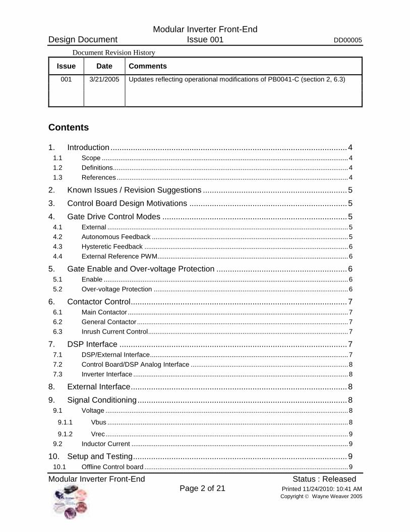
Document Revision History
Issue Date Comments
001 3/21/2005 Updates reflecting operational modifications of PB0041-C (section 2, 6.3)
Contents
1. Introduction ......................................................................................................... 4
1.1 Scope ..................................................................................................................................... 4
1.2 Definitions............................................................................................................................... 4
1.3 References ............................................................................................................................. 4
2. Known Issues / Revision Suggestions ................................................................ 5
3. Control Board Design Motivations ...................................................................... 5
4. Gate Drive Control Modes .................................................................................. 5
4.1 External .................................................................................................................................. 5
4.2 Autonomous Feedback .......................................................................................................... 5
4.3 Hysteretic Feedback .............................................................................................................. 6
4.4 External Reference PWM ....................................................................................................... 6
5. Gate Enable and Over-voltage Protection .......................................................... 6
5.1 Enable .................................................................................................................................... 6
5.2 Over-voltage Protection ......................................................................................................... 6
6. Contactor Control ................................................................................................ 7
6.1 Main Contactor ....................................................................................................................... 7
6.2 General Contactor .................................................................................................................. 7
6.3 Inrush Current Control ............................................................................................................ 7
7. DSP Interface ..................................................................................................... 7
7.1 DSP/External Interface ........................................................................................................... 7
7.2 Control Board/DSP Analog Interface ..................................................................................... 8
7.3 Inverter Interface .................................................................................................................... 8
8. External Interface ................................................................................................ 8
9. Signal Conditioning ............................................................................................. 8
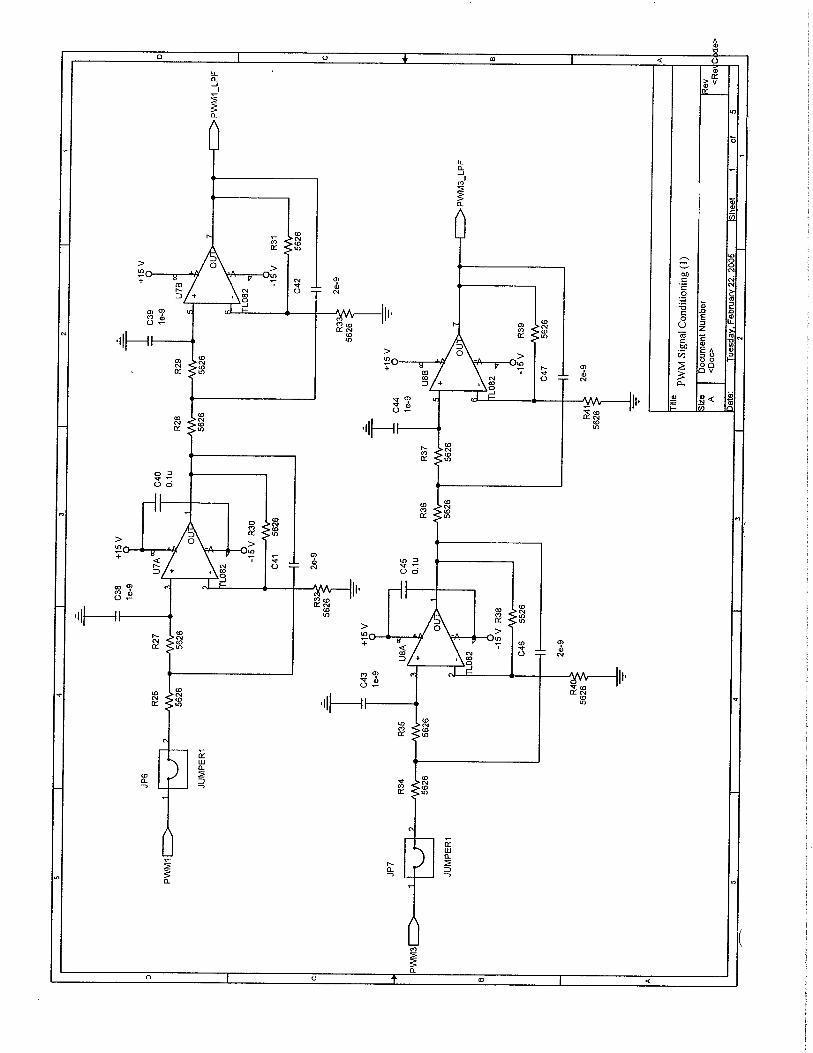
9.1 Voltage ................................................................................................................................... 8
9.1.1 Vbus .................................................................................................................................. 8
9.1.2 Vrec ................................................................................................................................... 9
9.2 Inductor Current ..................................................................................................................... 9
10. Setup and Testing ............................................................................................... 9
10.1 Offline Control board .............................................................................................................. 9
Modular Inverter Front-End Design Document Issue 001 DD00005
Modular Inverter Front-End Status : Released Page 3 of 21 Printed 11/24/2010: 10:41 AM
Copyright Wayne Weaver 2005
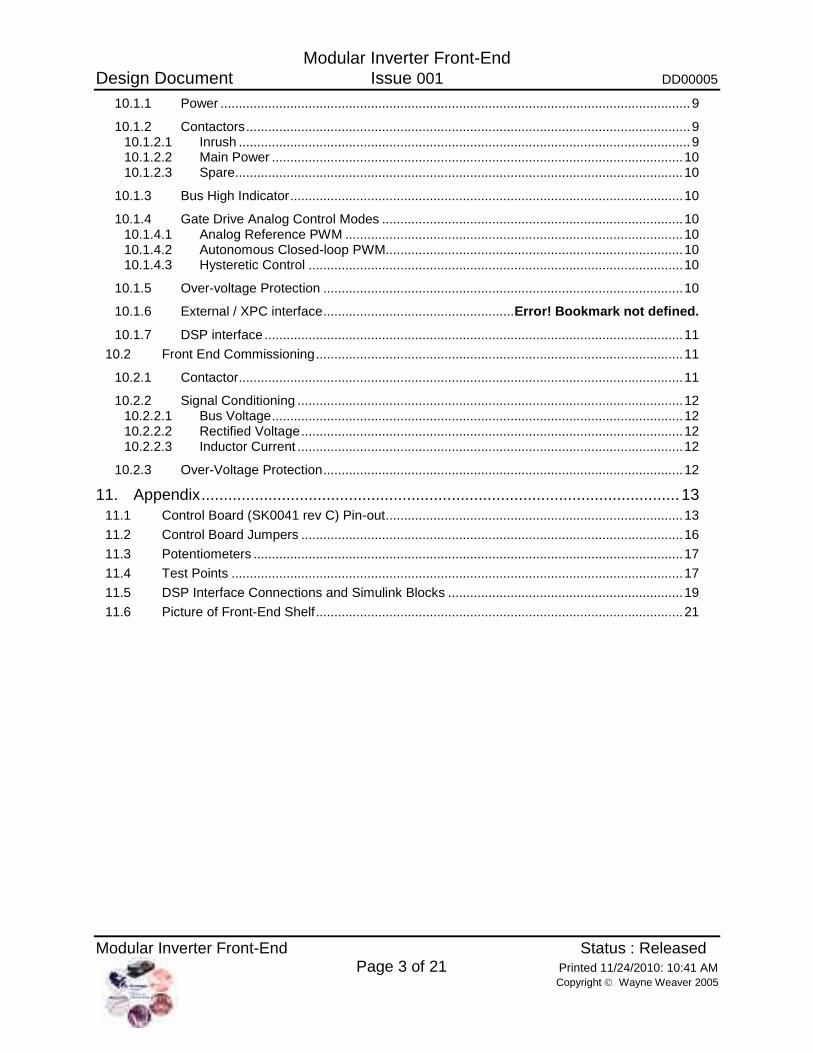
10.1.1 Power ................................................................................................................................ 9
10.1.2 Contactors ......................................................................................................................... 9 10.1.2.1 Inrush ........................................................................................................................... 9 10.1.2.2 Main Power ................................................................................................................ 10 10.1.2.3 Spare.......................................................................................................................... 10
10.1.3 Bus High Indicator ........................................................................................................... 10
10.1.4 Gate Drive Analog Control Modes .................................................................................. 10 10.1.4.1 Analog Reference PWM ............................................................................................ 10 10.1.4.2 Autonomous Closed-loop PWM ................................................................................. 10 10.1.4.3 Hysteretic Control ...................................................................................................... 10
10.1.5 Over-voltage Protection .................................................................................................. 10
10.1.6 External / XPC interface .................................................... Error! Bookmark not defined.
10.1.7 DSP interface .................................................................................................................. 11
10.2 Front End Commissioning .................................................................................................... 11
10.2.1 Contactor ......................................................................................................................... 11
10.2.2 Signal Conditioning ......................................................................................................... 12 10.2.2.1 Bus Voltage ................................................................................................................ 12 10.2.2.2 Rectified Voltage ........................................................................................................ 12 10.2.2.3 Inductor Current ......................................................................................................... 12
10.2.3 Over-Voltage Protection .................................................................................................. 12
11. Appendix ........................................................................................................... 13
11.1 Control Board (SK0041 rev C) Pin-out ................................................................................. 13
11.2 Control Board Jumpers ........................................................................................................ 16
11.3 Potentiometers ..................................................................................................................... 17
11.4 Test Points ........................................................................................................................... 17
11.5 DSP Interface Connections and Simulink Blocks ................................................................ 19
11.6 Picture of Front-End Shelf .................................................................................................... 21

Modular Inverter Front-End Design Document Issue 001 DD00005
Modular Inverter Front-End Status : Released Page 4 of 21 Printed 11/24/2010: 10:41 AM
Copyright Wayne Weaver 2005
1. Introduction
This project provides ac to dc conversion module to supply the motor inverter stage of the project.
However the load of the front-end is not necessarily limited to the modular inverter. For research
purposes the front-end could supply power to any required dc load.
1.1 Scope
The front-end module was designed as half of the modular motor inverter project. The input to the
front end is an ac power source and the output is a stable dc bus. The input ac power source can be
a single or three phase source.
Because of the need to process high power levels all power processing devices are not physically
located on the control board. The rectification device, converter switches and filtering devices are
stand alone.
1.2 Definitions
Control Board – SK0041 rev C PCB that controls the contactors and gate drive of the front end
unit.
DSP Daughter Board – SK0045 rev 1 that can be used as intelligent control and connects to the
control board via J12, J13, J14, and J16.
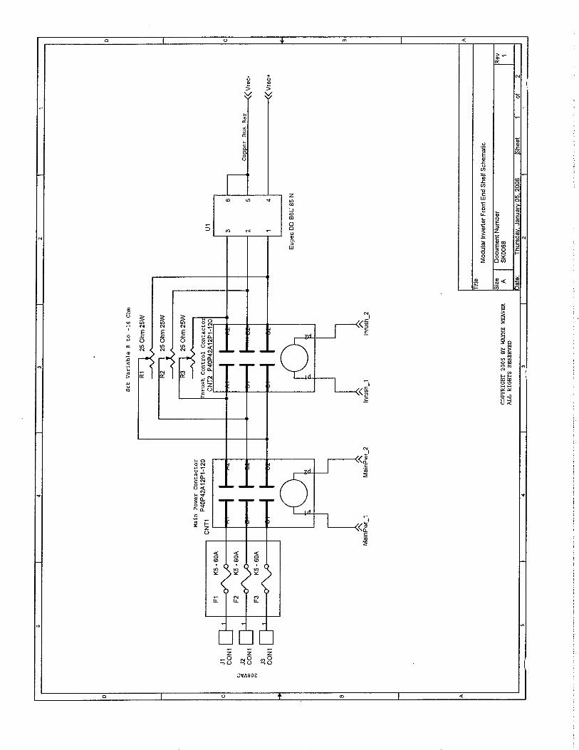
Front-End Shelf – Bottom shelf of the modular inverter box that contains all the 208 3phase ac to
400Vdc hardware.
1.3 References
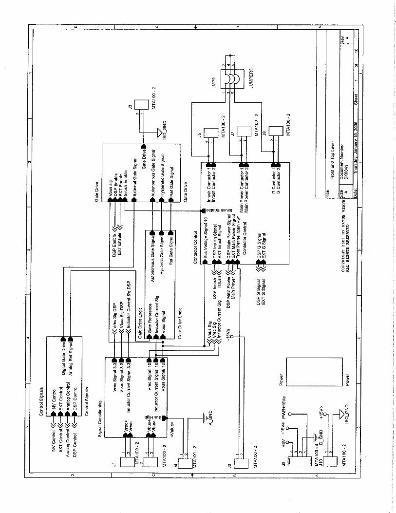
Front End Control Board Schematic: SK0041 rev C
Front End Control Board Layouts: PB0041 rev C
Front End Shelf Schematic: SK0068 rev 1
DSP Daughter Board Schematic: SK0054 rev 1
DSP Daughter Board Layout: PB0054 rev A
Modular Inverter Control Board Design Document DD00007-000
Analog PWM Daughterboard DD00008-000
eZDSP TMS320F28121 DSP Daughterboard DD00009-000
Modular Inverter Power Stage DD00010-000

Modular Inverter Front-End Design Document Issue 001 DD00005
Modular Inverter Front-End Status : Released Page 5 of 21 Printed 11/24/2010: 10:41 AM
Copyright Wayne Weaver 2005
2. Known Issues / Revision Suggestions
1. Ground Pins 4&5 of U3 are not connected to the board analog ground. A jumper wire
needs to be soldered from these pins to ground to ensure proper operation and limit the
voltage applied to the GPIO of the eZDSP Board.
2. The 3.3V regulator (U21) has a bad placement on the PCB. The heat sink interferes with
R27 and the DSP Daughter board.
3. Test points should be added at Bus high indicator (U26A-1) and the time delay for the
inrush current control (R4-2).
4. For PB0041-C the Inrush contactor control logic is triggered off of the Vbus signal. While
the bus capacitor is discharging after shutdown this causes an excessive amount of time
before the inrush resistors are switched back in line in preparation of a restart. A better way
is to use the Vrec signal since the voltage level drops quickly after shutdown. A
modification to board PB0041-C is to cut trace from D21-1/U1-3 and jumper between U1-3
and D17-1.
3. Control Board Design Motivations
The control board was designed for maximum flexibility in the control of the gate of the front-end
unit. Three analog gate drive signal schemes are on the board. Control signals external to the
board can be used including from the DSP daughter board, Matlab xPC, from the inverter stage,
or other sources. Digital control signals can be buffered and filtered in order to accept a broader
range of signal types. A spare contactor control was included for use in experiments that may
involve simulating a ‘fault’ on the system. The inductor current sensor LA55-P was chosen
because it prevents the need for high voltage high current of the main power flow to go through
the control board.
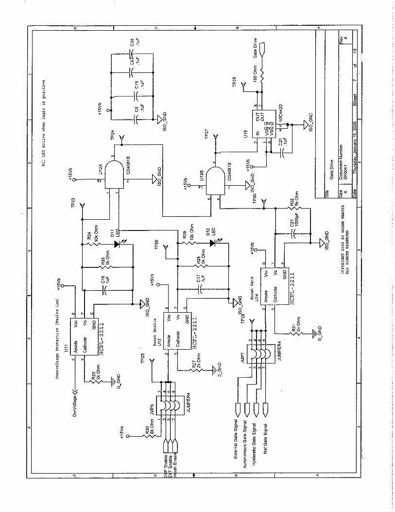
4. Gate Drive Control Modes
Three modes of control are designed with analog circuitry on the control board. In addition other
methods can be implemented via external interfaces. The gate drive signal is selected by JMP7 then
optically isolated through U14 before being gated by enable logic (section 5.1) and over-voltage
protection (section 5.2). If the gate drive is enabled then MIC4420 U15 drives the gate connected
to MTA100 J3.
4.1 External
An externally generated gate signal can be used to drive the converter gate. This signal can come
from a connected DSP, the inverter stage, or some other external source (J15) and is selected by
JMP4. Since the quality and voltage range of said signal is unknown, it is digitally buffered by an
MIC4420 (U9 sheet 5). The MIC4420 can accept a wide range of inputs and standardize the output
signal to the +15V board source regulated by zener D8.
4.2 Autonomous Feedback

Modular Inverter Front-End Design Document Issue 001 DD00005
Modular Inverter Front-End Status : Released Page 6 of 21 Printed 11/24/2010: 10:41 AM
Copyright Wayne Weaver 2005
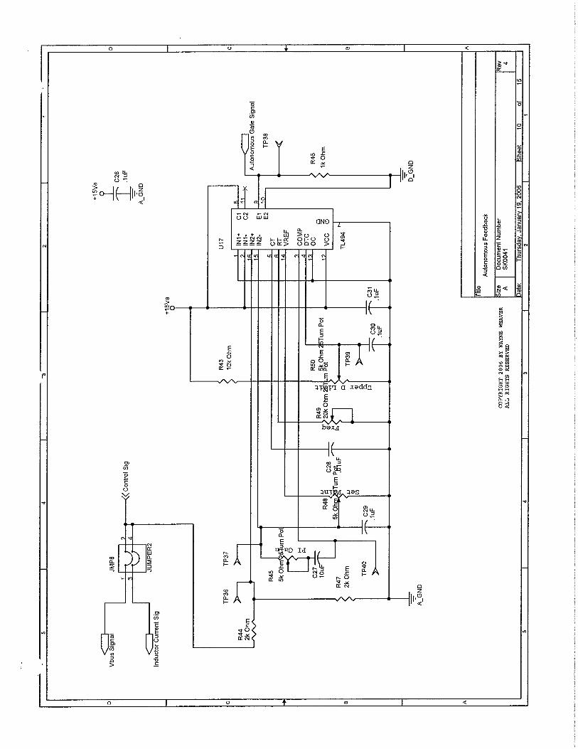
This mode is laid out on sheet 10 of SK0041C. In this control mode no external interface is
required. The controlled system variable can be either the bus voltage or inductor current (chosen
by JMP8). The chosen variable is compared to a reference set by R48, and then using a PI gain is
generated into PWM by TL494 chip U17. The frequency of the PWM signal is controlled by R49.
The gain of the PI loop is controlled by R45, with a time constant dictated by C27. Since the
system was designed primarily around a boost converter, a upper limit on the PWM duty cycle was
built into the circuit. The upper limit on the duty cycle is controlled by R50.
As an example: If the user wants to control the desired bus voltage to be 400Vdc, then JMP8
should be in 1-2 position. Adjust R48 so that the voltage on TP37=400V*(.013/2)=2.6V.
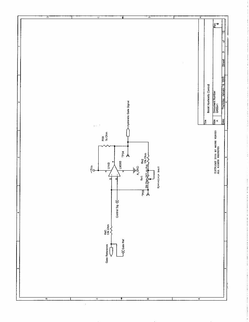
4.3 Hysteretic Feedback
This mode is laid out on sheet 9 of SK0041C. The controlled system variable can be either the bus
voltage or inductor current (chosen by JMP8). For example, if the dc-dc converter is a boost, then
the inductor current would be chosen, and if the converter is a buck, then the bus voltage can be
used. This mode uses an externally supplied reference signal compared to the system variable
through a Schmitt trigger hysteretic circuit to generate the gate switching signals. The hysteretic
band around the reference signal is controlled by R41.
4.4 External Reference PWM
This mode is laid out on sheet11 of SK0041C. This is an open loop control mode that uses an
externally supplied reference to generate the PWM signal via a TL494 (U18). R56 trims the
references signal. R57 controls the frequency of the generated PWM, and R59 sets an upper limit
on the PWM duty cycle.
5. Gate Enable and Over-voltage Protection
The gate drive must be enabled by and enabling circuit, and the over-voltage protection circuit.
These signals are gated by CMOS AND gate U12 before passing to the gate drive U15.
5.1 Enable
The converter gate enable signal is chosen among three options: bypass, DSP, external, and inrush
control enable. The selection is by JMP6 then is optically isolated before being logically gated
with the over-voltage protection signal and the gate signals. The bypass jumper setting
permanently enables the gate.
5.2 Over-voltage Protection
Because a boost converter is unstable at light loads, over-voltage protection is required to keep the
bus voltage from running away while the inverter stage or an alternative load is not active. This
situation typically occurs during start-up, where the front end would be active before the load.
Alternatively, a ballast load is required on the dc bus, usually in the form of a power resistor. This
circuitry is shown on sheet 8 of SK0041, and consists of a Schmitt trigger hysteretic circuit. R34
sets the threshold, and R37 controls the band around the threshold. When the bus voltage exceeds
the high threshold band, the gate is disabled until the voltage falls below the low band.
Modular Inverter Front-End Design Document Issue 001 DD00005
Modular Inverter Front-End Status : Released Page 7 of 21 Printed 11/24/2010: 10:41 AM
Copyright Wayne Weaver 2005
6. Contactor Control
Because of the potential for relatively high voltage (>200Vac) and high power (>100W)
mechanical contactors are required to control the flow of power at the ac input of the front-end
module. All 3 contactor control contacts can share a single power source via selection of JMP9.
The connections of the main power contactor and inrush current control contactor can be seen in
SK0068. Connections for the general contactor are left up to the user, based on usage.
6.1 Main Contactor
The main contactor is the primary power disconnect of the front-end module. The control board
circuit is laid out on sheet 4 of SK0041. One of three sources can be chosen to actuate the main
contactor through JMP3. The first is from a connection to a switch on the front panel of the
module J6. The second is a signal from a connected DSP, and the third is from an alternative
external source J15. Since all three possible sources are not necessarily of the same signal type, the
chosen signal is buffered through a MIC4420 (U7). Because larger mechanical contactors usually
have a 120Vac coil, a PCB relay (U8) is actuated by the signal buffer. The connection to the PCB
relay can then be connected to the appropriate power source and the contactor coil.
6.2 General Contactor
For research purposes circuitry similar to that described in section 6.1 is included to actuate a spare
or general contactor. This general contactor is signaled by either the DSP or an external signal
through JMP2. Foreseeable uses of the general contactor include switching ‘fault’ resistors into the
ac power lines to simulate a fault in the system, to study the response of the converter.
6.3 Inrush Current Control
Due to bus capacitance, a large inrush current can result when the main power is initially
connected. To mitigate this, circuitry on sheet3 of SK0041 actuates a contactor to switch in extra
resistance to the ac power lines, until the bus capacitance is appropriately charged. This circuit
compares the conditioned bus voltage signal described in section 9.1.2 through an adjustable (R4)
time delay with a reference threshold (R1) and hysteretic band (R5). When the rectified voltage
has met the requirements then the inrush contactor is actuated, effectively switching out the added
line resistance.
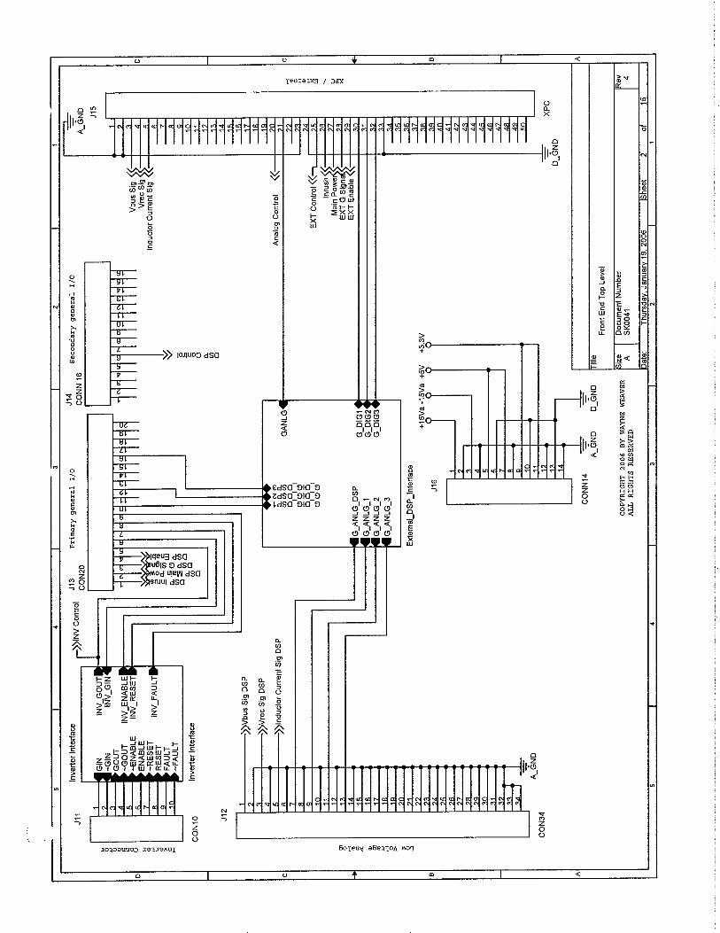
7. DSP Interface
The front-end module is designed to interface and operate with Modular Inverter DSP Daughter
Board (SK0054). The control board can be configured to accept a direct gate drive signal from the
DSP, or to filter the DSP PWM into an analog signal for use as a reference in the analog gate logic
of section 4.
7.1 DSP/External Interface

Modular Inverter Front-End Design Document Issue 001 DD00005
Modular Inverter Front-End Status : Released Page 8 of 21 Printed 11/24/2010: 10:41 AM
Copyright Wayne Weaver 2005
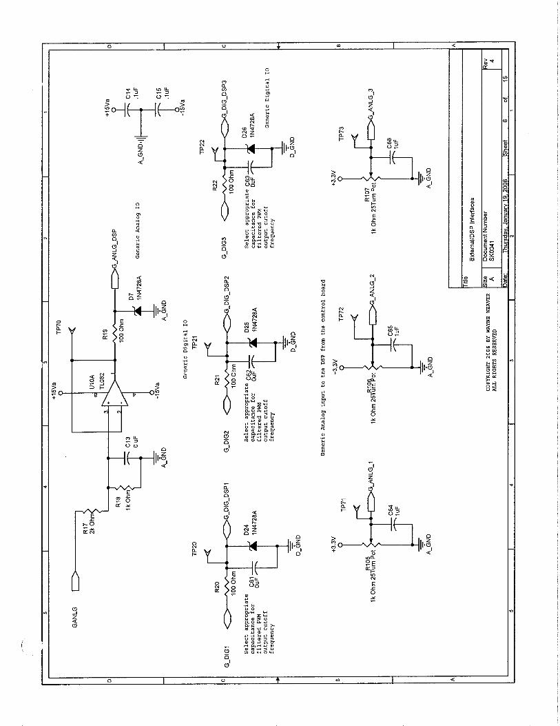
Circuitry shown on sheet 6 of SK0041_C is the interface between the DSP and any given external
source. Three generic digital IO points are provided, as well as analog signal from the external
source to the DSP. The analog signal is voltage divided from a 0-10V range to a 0-3V range, then
buffered with a op-amp follower (U10).
7.2 Control Board/DSP Analog Interface
Three generic analog reference signals to the DSP daughter board are shown on sheet 6 of SK0041.
R105, 106 and 107 trim a 0-3.3V signal to the DSP on VBUS_LOW, T1_LOW, and T2_LOW
shown on Sheet 2 of SK0054. These signals can be used to adjust DSP parameters without a
change in DSP programming.
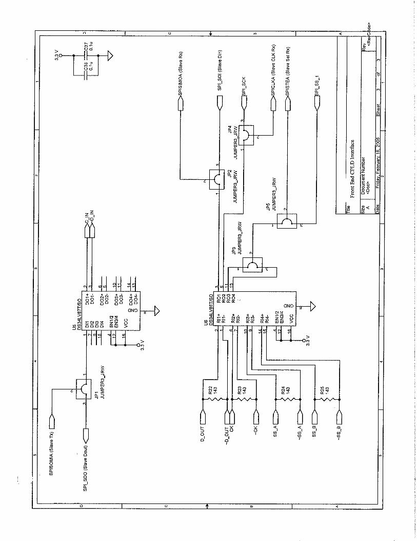
7.3 Inverter Interface
The DSP unit can communicate with the inverter stage via differential IO lines generated by a
DS26L32AC (U20) and DS26LS31C (U19) shown on sheet 12. Four IO lines are from the Inverter
to the front end. They are ENABLE, FAULT, RESET, and GENERIC. The functionality of these
IO is up to the user to implement. A single IO line from the front-end to the inverter is also
provided
8. External Interface
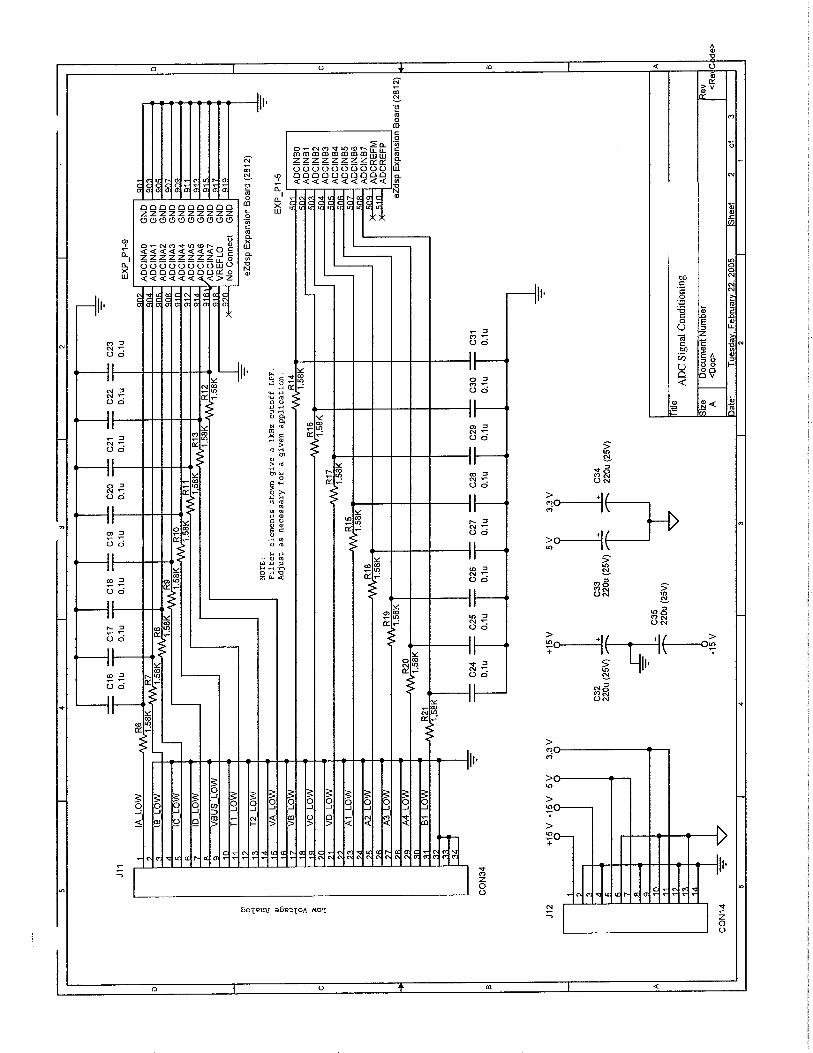
The external interface connection J15 was primarily designed to operate with a Matlab xPC Target
system using a National Instruments 6025E data acquisition card. However, any external source or
instrument can be used if the proper pinout (see section 11.1) is used.
9. Signal Conditioning
9.1 Voltage
Both voltage measurements are accomplished using op-amp (TL082) gain to bring anticipated
measurements into the desired range. The first stage brings the voltage to a 0-10V range for use by
external xPC. A second stage divides the signal again by a third to a 0-3.3V range for use by the
DSP. Both stages have clamping Zener diodes to guarantee the voltage range is not violated. In
addition, a position for a filtering capacitor is provided at the input to the second stage.
Note: Resistances can be changed for any range of input voltage.
9.1.1 Vbus
For a nominal of Vbus=400 the nominal output of stage 1 is 5V. Using standard resistor values:
R80=R82=1M
R79=R83=13k
This yield a nominal output of 5.2V and maximum input voltage of 769V for the 0-10V
conditioned signal.

Modular Inverter Front-End Design Document Issue 001 DD00005
Modular Inverter Front-End Status : Released Page 9 of 21 Printed 11/24/2010: 10:41 AM
Copyright Wayne Weaver 2005
9.1.2 Vrec
For a nominal of Vrec=285 the nominal output of stage 1 is 5V. using standard resistor values:
R80=R82=1M
R79=R83=18k
This yield a nominal output of 5.13V and maximum input voltage of 555V for the 0-10V
conditioned signal.
9.2 Inductor Current
The LA55-P current sensor has a 0-50A input range (U23). The output of this sensor is a current
source at 1/1000 of the input. A burden resistor of 100 (R90) is used to produce a voltage signal.
The voltage signal is then amplified with adjustable gain set by R91. The measurement range can
also be modified by increasing the number of turns through the sensors window. However, using
12 AWG wire, 6 turns is the maximum.
10. Setup and Testing
The following are procedures for setting up and testing the control board (PB0041_C) and the
complete front end shelf (SK0068). These procedures are not all inclusive; rather they establish a
framework for future users to start with. All setup and test procedures are assuming a nominal bus
voltage of 400V and 3-phase 208V input to the rectifier.
10.1 Offline Control board
This section includes procedures to test and setup the functionality of the control board alone
(PB0041_C). All procedures are done offline (not connected as in SK0068). The only connections
to the board should be power (J9, J10), and those outlined below.
10.1.1 Power
Connect power to J9 (see section 11.1 for pinout). LED’s D13, D15 and D16 should light up.
10.1.2 Contactors
10.1.2.1 Inrush
1. Switch Out resistors at Vbus>200V (200*(13000/1000000)=2.6V=SO)
2. Switch In resistors at Vbus<20V (200*(13000/1000000)=.26V=SI)
3. Connect signal generator to TP64 with square signal ~1Hz, 4Vp-p, 5V offset
4. Connect Scope
a. Ch1 TP64
b. Ch2 R2-1
c. Ch3 TP5
5. Jumper JMP1 1-2
6. Adjust R4 until ch2 crosses SO at desired delay (250ms)
7. Adjust R1, R5 until desired SO and SI achieved (iterative)
Modular Inverter Front-End Design Document Issue 001 DD00005
Modular Inverter Front-End Status : Released Page 10 of 21 Printed 11/24/2010: 10:41 AM
Copyright Wayne Weaver 2005
10.1.2.2 Main Power
5. Remove jumper on JMP3
6. Jumper +5 to TP13
7. D3 should be lit and Relay U8 closed
10.1.2.3 Spare
1. Remove jumper on JMP2
2. Jumper +5 to TP9
3. D2 should lit on and Relay U6 closed
10.1.3 Bus High Indicator
1. Jumper +1V (1V/.013= 76Vbus) to TP64
2. Adjust R102 threshold until D23 is lit
10.1.4 Gate Drive Analog Control Modes
10.1.4.1 Analog Reference PWM
1. Jumper +5 to TP19
2. Scope TP41
3. Adjust frequency R57 ) to 10kHz
4. Adjust upper limit to ~35% R59
5. Trim reference with R56
10.1.4.2 Autonomous Closed-loop PWM
1. Jumper +5 to post 2 on JMP8
2. Scope TP38
3. Adjust frequency (R49) to 10kHz
4. Max Duty Cycle (R50) ~35%
10.1.4.3 Hysteretic Control
1. Connect signal generator (sinusoid,100Hz, 1Vp-p, 2.5V offset) to post 2 of JMP8
2. Connect +5 to TP19
3. Scope TP35 (band) and TP34 (output)
4. Adjust hysteretic band (R41)
10.1.5 Over-voltage Protection
1. Connect signal generator (sinusoid,100Hz, 1Vp-p, 2.5V offset) to TP64
2. Set threshold and band for hysteretic (R34, R37)
a. Over voltage at 420 (420*(13000/1000000)=5.46V)
b. Resume at 380 (380*(13000/1000000)=4.94V)

Modular Inverter Front-End Design Document Issue 001 DD00005
Modular Inverter Front-End Status : Released Page 11 of 21 Printed 11/24/2010: 10:41 AM
Copyright Wayne Weaver 2005
3. Verify at TP32
4. Power gate drive (PWR-B)
5. Enable gate (JMP6 1-2)
6. Use Reference or autonomous PWM circuit to generate pwm to Gate drive.
7. Verify over-voltage protection (it is disabling gate) at TP 28.
10.1.6 DSP interface
Testing of the analog functions of the board should be done and verified first before the eZDSP is
used. The programming of the eZDSP board can be accomplished via the Matlab Simulink RTW
toolbox, or manually via the code composer studio (see eZDSP TMS320F28121 DSP
Daughterboard design document DD00009-000 for details)
It is recommended that the control of the inrush current contactor and main power contactor stay a
function of the analog control board. However, these function can be controlled by the eZDSP via
a change in jumper (see section 11.2).
10.2 Front End Commissioning
It is assumed that all desired control board functions were setup, tested and verified by the user
before the control board is integrated into the front end shelf unit (SK0068).
WARNING, operate unit with great caution, nominal
voltages are at dangerous levels.
10.2.1 Contactor
Connect system as indicated in SK0068, with exception of the connection power to inverter unit
(use resistive load).
1. Press main power button on front panel, and verify power and inrush current contactor
operation.
2. Make adjustments to delay (R4) and thresholds (R4,R1) as needed.
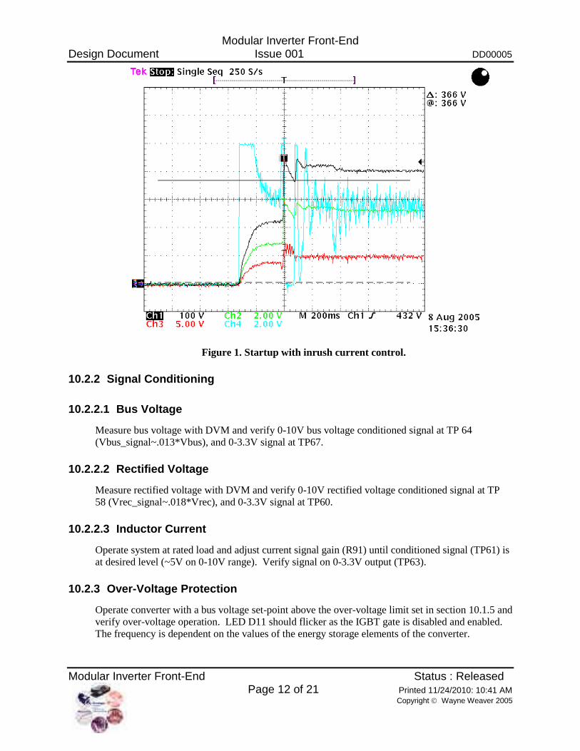
Figure 1 shows oscilloscope screen capture of a startup with inrush current control, the
autonomous feedback control is used to drive the IGBT gate. Channel 1 is bus voltage measured
directly from a differential scope probe, channel 2 is the conditioned bus voltage signal from TP64
of the control board, channel 3 is the rectified voltage conditioned signal from TP58 and channel 4
is the conditioned inductor current signal on TP61. Note at time 0sec when the inrush resistors are
first switched out, the bus voltage overprotection disables the gate and the voltage drops until it
reaches the turn on limit, then the system settles to the nominal set-point.
Modular Inverter Front-End Design Document Issue 001 DD00005
Modular Inverter Front-End Status : Released Page 12 of 21 Printed 11/24/2010: 10:41 AM
Copyright Wayne Weaver 2005
Figure 1. Startup with inrush current control.
10.2.2 Signal Conditioning
10.2.2.1 Bus Voltage
Measure bus voltage with DVM and verify 0-10V bus voltage conditioned signal at TP 64
(Vbus_signal~.013*Vbus), and 0-3.3V signal at TP67.
10.2.2.2 Rectified Voltage
Measure rectified voltage with DVM and verify 0-10V rectified voltage conditioned signal at TP
58 (Vrec_signal~.018*Vrec), and 0-3.3V signal at TP60.
10.2.2.3 Inductor Current
Operate system at rated load and adjust current signal gain (R91) until conditioned signal (TP61) is
at desired level (~5V on 0-10V range). Verify signal on 0-3.3V output (TP63).
10.2.3 Over-Voltage Protection
Operate converter with a bus voltage set-point above the over-voltage limit set in section 10.1.5 and
verify over-voltage operation. LED D11 should flicker as the IGBT gate is disabled and enabled.
The frequency is dependent on the values of the energy storage elements of the converter.
Modular Inverter Front-End Design Document Issue 001 DD00005
Modular Inverter Front-End Status : Released Page 13 of 21 Printed 11/24/2010: 10:41 AM
Copyright Wayne Weaver 2005
11. Appendix
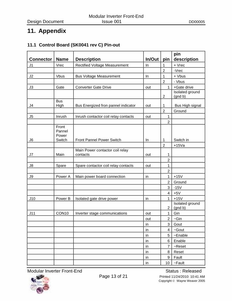
11.1 Control Board (SK0041 rev C) Pin-out
Connector Name Description In/Out pin pin description
J1 Vrec Rectified Voltage Measurement In 1 + Vrec
2 -Vrec
J2 Vbus Bus Voltage Measurement In 1 + Vbus
2 - Vbus
J3 Gate Converter Gate Drive out 1 +Gate drive
2 Isolated ground (gnd b)
J4 Bus High Bus Energized fron pannel indicator out 1 Bus High signal
2 Ground
J5 Inrush Inrush contactor coil relay contacts out 1
2
J6
Front Pannel Power Switch Front Pannel Power Switch In 1 Switch in
2 +15Va
J7 Main Main Power contactor coil relay contacts out 1
2
J8 Spare Spare contactor coil relay contacts out 1
2
J9 Power A Main power board connection in 1 +15V
2 Ground
3 -15V
4 +5V
J10 Power B Isolated gate drive power in 1 +15V
2 Isolated ground (gnd b)
J11 CON10 Inverter stage communications out 1 Gin
out 2 ~Gin
in 3 Gout
in 4 ~Gout
in 5 ~Enable
in 6 Enable
in 7 ~Reset
in 8 Reset
in 9 Fault
in 10 ~Fault
Modular Inverter Front-End Design Document Issue 001 DD00005
Modular Inverter Front-End Status : Released Page 14 of 21 Printed 11/24/2010: 10:41 AM
Copyright Wayne Weaver 2005
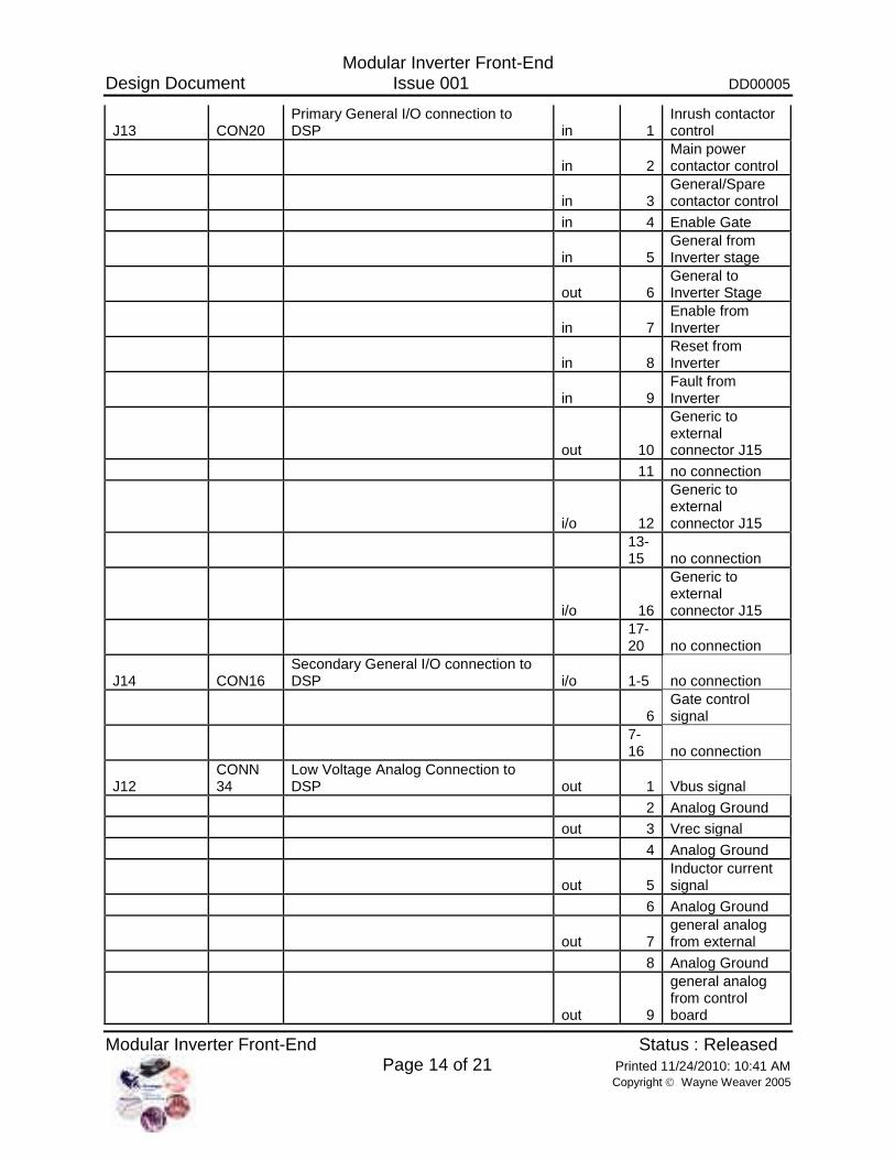
J13 CON20 Primary General I/O connection to DSP in 1
Inrush contactor control
in 2 Main power contactor control
in 3 General/Spare contactor control
in 4 Enable Gate
in 5 General from Inverter stage
out 6 General to Inverter Stage
in 7 Enable from Inverter
in 8 Reset from Inverter
in 9 Fault from Inverter
out 10
Generic to external connector J15
11 no connection
i/o 12
Generic to external connector J15
13-15 no connection
i/o 16
Generic to external connector J15
17-20 no connection
J14 CON16 Secondary General I/O connection to DSP i/o 1-5 no connection
6 Gate control signal
7-16 no connection
J12 CONN 34
Low Voltage Analog Connection to DSP out 1 Vbus signal
2 Analog Ground
out 3 Vrec signal
4 Analog Ground
out 5 Inductor current signal
6 Analog Ground
out 7 general analog from external
8 Analog Ground
out 9
general analog from control board
Modular Inverter Front-End Design Document Issue 001 DD00005
Modular Inverter Front-End Status : Released Page 15 of 21 Printed 11/24/2010: 10:41 AM
Copyright Wayne Weaver 2005
10 Analog Ground
out 11
general analog from control board
12 Analog Ground
out 13
general analog from control board
14-34 Analog Ground
J16 CONN 14 DSP Power Connection out 1 +15V
2 Analog Ground
out 3 -15V
4 Analog Ground
out 5 +5V
6 Digital Ground
out 7 +5V
8 Analog Ground
out 9 +3.3V
10 Digital Ground
out 11 +3.3V
12 Analog Ground
13 Digital Ground
14 Analog Ground
J15 XPC External (XPC) i/o connection 1 Analog Ground
2 Analog Ground
out 3 Vbus signal
out 4 Vrec signal
out 5 Inductor current signal
6-19 no connection
In 20 Analog reference
in 21 General DSP analog signal
22 no connection
in 23 Analog Ground
in 24 Digital Ground
in 25 External Digital Control signal
in 26 Inrush contactor control
in 27 Main power contactor control
in 28 General/Spare contactor control
Modular Inverter Front-End Design Document Issue 001 DD00005
Modular Inverter Front-End Status : Released Page 16 of 21 Printed 11/24/2010: 10:41 AM
Copyright Wayne Weaver 2005
in 29 Enable Gate
i/o 30 Generic Digital io to DSP
i/o 31 Generic Digital io to DSP
i/o 32 Generic Digital io to DSP
33 Digital Ground
34-50 no connection
11.2 Control Board Jumpers
Jumper Sheet Description Pos 1-2 3-4 5-6 7-8
JMP1 3 Source of Inrush Control
On-board analog comparator DSP External
JMP2 4
Spare Contactor Control DSP External
JMP3 4
Main Power Contactor Control
Front Panel Switch DSP External
JMP4 5 Digital Buffer Input
Inverter Stage DSP External
JMP5 5
Analog Reference Signal Source
Filtered Digital Buffer External
JMP6 7 Gate Enable Bypass DSP External
On-Board Inrush Control
JMP7 7 Gate Drive Source External
Autonomous PWM Hysteretic
Referenced PWM
JMP8 10
Control Variable Selection
Bus Voltage
Inductor Current
Modular Inverter Front-End Design Document Issue 001 DD00005
Modular Inverter Front-End Status : Released Page 17 of 21 Printed 11/24/2010: 10:41 AM
Copyright Wayne Weaver 2005
11.3 Potentiometers
Pot Sheet Value Function
R1 3 10k Threshold value of schmitt trigger comparator inrush current contactor
R3 3 2M band for schmitt trigger comparator inrush current contactor
R4 3 100k Time delay of inrush contactor
R34 8 2k nominal value for schmitt trigger comparator for bus over-voltage protection
R37 8 2M band forschmitt trigger comparator for bus over-voltage protection
R41 9 2M band for schmitt trigger comparator of hysteretic gate control mode
R45 10 5k PI gain for autonomous pwm gate drive control mode
R48 10 5k Bus Voltage set-point for autonomous pwm gate drive control mode
R49 10 10k Frequency of PWM in autonomous PWM gate drive control mode
R50 10 5k Duty cycle upper limit for autonomous PWM gate drive control mode
R56 11 5k Reference trim for external reference PWM gate drive control mode
R57 11 100k Frequency of PWM in external reference PWM gate drive control mode
R59 11 5k Duty cycle upper limit for external reference PWM gate drive control mode
R91 14 50k Gain for inductor current sensor
R102 15 2k Threshold for front panel bus high indicator
11.4 Test Points
Test Point # Sheet Description
1 3 Threshold voltage of schmitt trigger comparator for inrush current control
2 3 Onboard analog inrush contactor signal
3 3 voltage band of schmitt trigger comparator for inrush current control
4 3 Input to inrush contactor driver
5 3 Output of inrush contactor driver
6 3 Inrush Relay contact 1
7 3 Inrush Relay contact 2
8 4 Spare Relay contact 1
9 4 Input to spare contactor driver
10 4 Output of spare contactor driver
11 4 Spare Relay contact 2
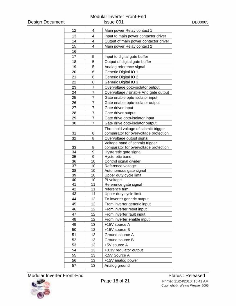
Modular Inverter Front-End Design Document Issue 001 DD00005
Modular Inverter Front-End Status : Released Page 18 of 21 Printed 11/24/2010: 10:41 AM
Copyright Wayne Weaver 2005
12 4 Main power Relay contact 1
13 4 Input to main power contactor driver
14 4 Output of main power contactor driver
15 4 Main power Relay contact 2
16
17 5 Input to digital gate buffer
18 5 Output of digital gate buffer
19 5 Analog reference signal
20 6 Generic Digital IO 1
21 6 Generic Digital IO 2
22 6 Generic Digital IO 3
23 7 Overvoltage opto-isolator output
24 7 Overvoltage / Enable And gate output
25 7 Gate enable opto-isolator input
26 7 Gate enable opto-isolator output
27 7 Gate driver input
28 7 Gate driver output
29 7 Gate drive opto-isolator input
30 7 Gate drive opto-isolator output
31 8 Threshold voltage of schmitt trigger comparator for overvoltage protection
32 8 Overvoltage output signal
33 8 Voltage band of schmitt trigger comparator for overvoltage protection
34 9 Hysteretic gate signal
35 9 Hysteretic band
36 10 Control signal divider
37 10 Reference voltage
38 10 Autonomous gate signal
39 10 Upper duty cycle limit
40 10 PI voltage
41 11 Reference gate signal
42 11 reference trim
43 11 Upper duty cycle limit
44 12 To inverter generic output
45 12 From inverter generic input
46 12 From inverter reset input
47 12 From inverter fault input
48 12 From inverter enable input
49 13 +15V source A
50 13 +15V source B
51 13 Ground source A
52 13 Ground source B
53 13 +5V source A
54 13 +3.3V regulator output
55 13 -15V Source A
56 13 +15V analog power
57 13 Analog ground

Modular Inverter Front-End Design Document Issue 001 DD00005
Modular Inverter Front-End Status : Released Page 19 of 21 Printed 11/24/2010: 10:41 AM
Copyright Wayne Weaver 2005
58 14 Vrec signal (0-10V)
59 14 Vrec + input
60 14 Vrec signal (0-3.3V)
61 14 Amplified current signal (0-10V)
62 14 Current sensor output
63 14 Amplified current signal (0-3.3V)
64 15 Vbus signal (0-10V)
65 15 Vbus + input
66 15 Vbus - input
67 15 Vbus signal (0-3.3V)
68 15 Bus high threshold (on 0-10V range)
11.5 DSP Interface Connections and Simulink Blocks
Function SK0041C SK0054 ezDSP
Simulink Embedded Target for TI C2000 DSP C
onn
ecto
r
Pin
Co
nn
ecto
r
Pin
Ju
mp
er
Co
nn
ecto
r
Pin
De
scrip
tion
Blo
ck
IO M
ux
Bit
Inrush contactor Control J13 1 J1 1 JP2 2-3 P8 23
SPI_SDI / SPISIMOA C28x GPIO DO GIOF 0
Main Contactor Control J13 2 J1 2 JP1 2-3 P8 24
SPI_SDO / SPISOMOA C28x GPIO DO GIOF 1
General Contactor Control J13 3 J1 3 JP4 2-3 P8 25
SPI_SCK / SPICLKA C28x GPIO DO GIOF 2
Gate Enable J13 4 J1 4 JP5 2-3 P8 26 SPI_SS_1 / SPISTEA C28x GPIO DO GIOF 3
Inverter stage generic communication in J13 5 J1 5 P4 2 XINT2/ADCSOC C28x GPIO DO GIOE 1
Inverter stage generic communication out J13 6 J1 6 P8 5 XINT1n/XBIOn C28x GPIO DO GIOE 0
Inverter stage enable J13 7 J1 7 P8 6 CAP1/QEP1 C28x GPIO DO GIOA 8
Inverter stage reset J13 8 J1 8 P8 7 CAP2/QEP2 C28x GPIO DO GIOA 9
Inverter stage fault J13 9 J1 9 P8 8 CAP3/QEP11 C28x GPIO DO GIOA 10
External Generic Communication 1 J13 10 J1 10 P8 9 PWM1 C28x GPIO DO GIOA 0
External Generic Communication 2 J13 12 J1 12 P8 11 PWM3 C28x GPIO DO GIOA 1
External Generic Communication 3 J13 16 J1 16 P8 15 T1PWM/TICMP C28x GPIO DO GIOA 6

Modular Inverter Front-End Design Document Issue 001 DD00005
Modular Inverter Front-End Status : Released Page 20 of 21 Printed 11/24/2010: 10:41 AM
Copyright Wayne Weaver 2005
Gate Drive Control J14 6 J5 6 P8 30 PWM7 C28xPWM or C28x GPIO DO
Output1 or GPIOB 0
Vbus Signal J12 1 J11 1 P9 2 ADCINA0 C28x ADC ADCINA0
Vrec Signal J12 3 J11 3 P9 4 ADCINA1 C28x ADC ADCINA1
Inductor Current J12 5 J11 5 P9 6 ADCINA2 C28x ADC ADCINA2
External Analog J12 7 J11 7 P9 8 ADCINA3 C28x ADC ADCINA3
Generic Analog (R105) J12 9 J11 9 P9 10 ADCINA4 C28x ADC ADCINA4
Generic Analog (R106) J12 11 J11 11 P9 12 ADCINA5 C28x ADC ADCINA5
Generic Analog (R107) J12 13 J11 13 P9 14 ADCINA6 C28x ADC ADCINA6
Modular Inverter Front-End Design Document Issue 001 DD00005
Modular Inverter Front-End Status : Released Page 21 of 21 Printed 11/24/2010: 10:41 AM
Copyright Wayne Weaver 2005
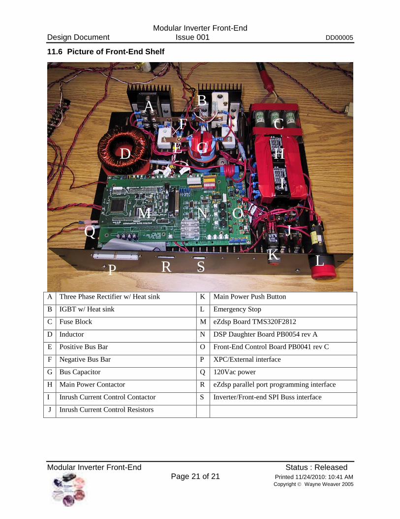
11.6 Picture of Front-End Shelf
A Three Phase Rectifier w/ Heat sink K Main Power Push Button
B IGBT w/ Heat sink L Emergency Stop
C Fuse Block M eZdsp Board TMS320F2812
D Inductor N DSP Daughter Board PB0054 rev A
E Positive Bus Bar O Front-End Control Board PB0041 rev C
F Negative Bus Bar P XPC/External interface
G Bus Capacitor Q 120Vac power
H Main Power Contactor R eZdsp parallel port programming interface
I Inrush Current Control Contactor S Inverter/Front-end SPI Buss interface
J Inrush Current Control Resistors
A B
C
D E
F
G H
I
J
U K L
M N O
P
Q
R S
Grainger Center for Electric Machinery and Electromechanics Department of Electrical and Computer Engineering
University of Illinois at Urbana-Champaign 1406 W. Green St.
Urbana, IL 61801
The information contained in this Document and the Appendices may not be copied, reproduced, distributed or stored in a retrieval system without the prior express written permission of the author.
Copyright Board of Trustees of the University of Illinois 2005. All Rights Reserved
Design Document
Modular Inverter Control Board
Reference: DD00007
Issue: 001
Status: Issued
Author: Z. Sorchini / J. Wells
Updated: Ali M. Bazzi / Kieran Levin / Paul Rancuret
Principal Investigator: J. Kimball
Created: June 23, 2005
Updated: Nov. 23, 2010
\\cts-file-02\power\DesignArchives\Documents\Design Documents\ DD00007-001 Modular Inverter Control Board.doc
Abstract:
This document briefly describes the functionality and characteristics of the control board for the
modular inverter.

Modular Inverter Control Board Design Document Issue 001 DD00007
Modular Inverter Control Board Status : Issued Page 2 of 10 Printed 11/24/2010: 10:42 AM
Copyright University of Illinois 2005
Document Revision History
Issue Date Comments
000 3/6/2006 Initial release. 001 11/23/2010 Testing procedure added.
Contents
1. Introduction ......................................................................................................... 3
1.1 Scope ..................................................................................................................................... 3
1.2 References ............................................................................................................................. 3
1.3 Known Issues ......................................................................................................................... 3
2. Main Board ......................................................................................................... 3
2.1 Power Stage Interface ............................................................................................................ 3
2.2 Interface Logic ........................................................................................................................ 4
2.2.1 CPLD ................................................................................................................................. 4
2.2.2 Microcontroller ................................................................................................................... 4
2.3 Analog Signal Conditioning .................................................................................................... 4
2.4 Digital Signal Conditioning ..................................................................................................... 5
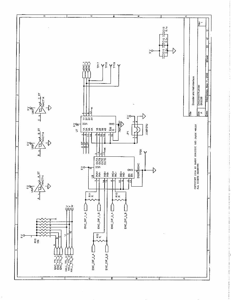
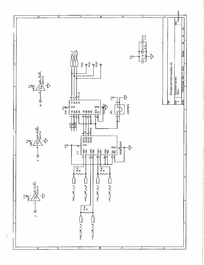
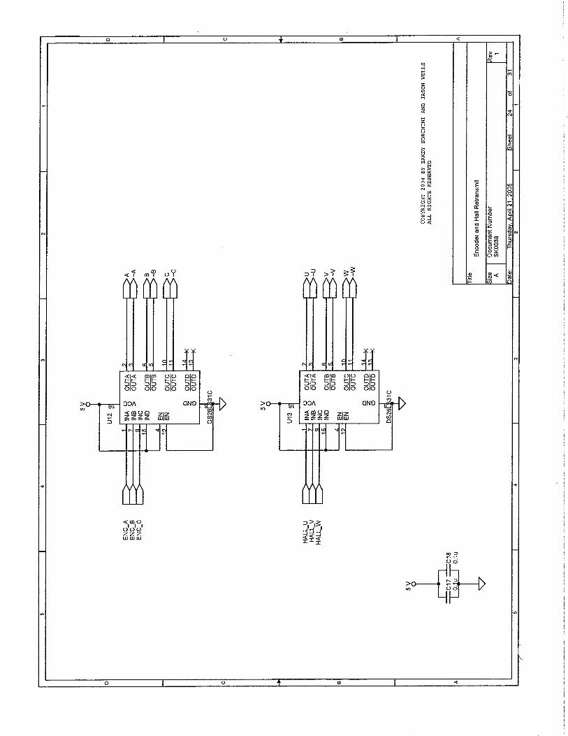
2.5 Encoder and Hall Sensor Interface ........................................................................................ 5
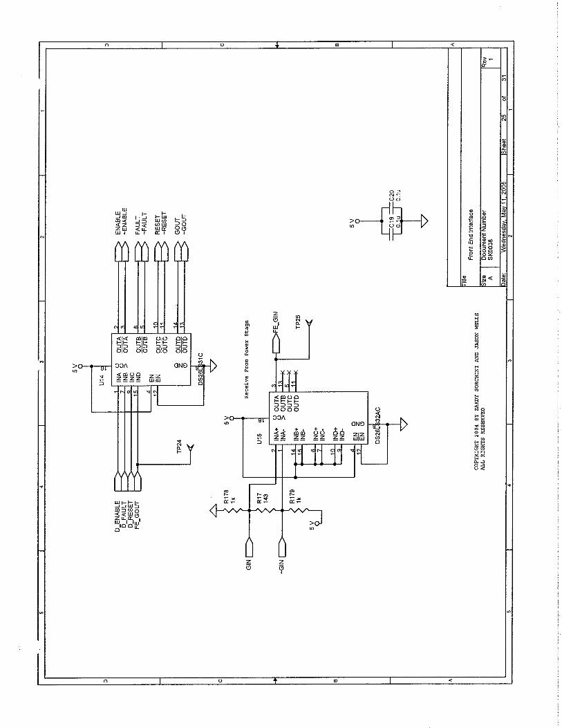
2.6 Front-End Interface ................................................................................................................ 5
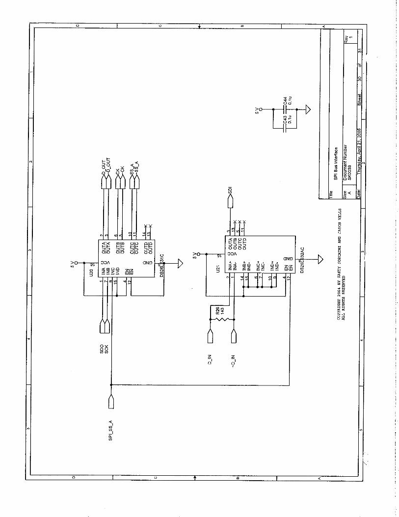
2.7 SPI Bus Interface ................................................................................................................... 5
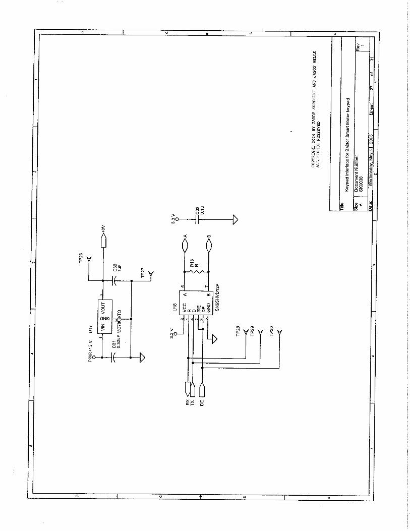
2.8 Keypad Interface .................................................................................................................... 5
2.9 Enable Signals ....................................................................................................................... 6
3. Daughter Board Interface .................................................................................... 6
3.1 Physical Layout ...................................................................................................................... 6
3.2 Digital Interface ...................................................................................................................... 6
3.3 Analog Interface ..................................................................................................................... 6
3.4 Power ..................................................................................................................................... 6
4. Control Board Testing Procedure ....................................................................... 7
4.1 Power Supply ......................................................................................................................... 7
4.2 DSP Control Signals .............................................................................................................. 8
4.3 DSP Analog Input Signals ...................................................................................................... 9

Modular Inverter Control Board Design Document Issue 001 DD00007
Modular Inverter Control Board Status : Issued Page 3 of 10 Printed 11/24/2010: 10:42 AM
Copyright University of Illinois 2005
1. Introduction
The control board for the modular inverter provides an interface between the power stage, the
front-end and the main control circuit (daughterboard). Analog information together with status
information is collected from the power stage and the front-end and is conditioned and made
available to the main control circuit (i.e., the daughterboard). The switching signals are routed to
the power stage. Additionally, interfaces for ISP peripherals, keypad, encoder and hall sensors are
available.
1.1 Scope
The control board is intended to be used as part of the modular inverter, together with the power
stage. Front-end is optional since an external dc source can be used. Primary use is for research.
Most of the functionality is available when the CPLD is properly programmed. The final user is
responsible for correctly programming the CPLD.
1.2 References
Schematic: SK0038 rev 2
Layout: PB0038 rev B
Specification document: SD0004, Modular Inverter System Specification
Front-end: SK0041 and PB0041
Power stage: SK0031 and PB0031
Analog PWM daughterboard: SK0048 and PB0048
DSP daughterboard: SK0054 and PB0054
1.3 Known Issues
There are no ground test points near the analog signal processing blocks.
The resistors specified in the schematic for the unipolar analog blocks, where the signal is reduced
to 3 V (voltage divider before the ouput buffer) are wrong. Resistor values of 23.2k and 10k should
work.
The bus current signal from the Inverter Board is never routed from the connector. If required, it
can be made available by cutting a trace (signal B1 from J17 pin 6 is recommended) and then
connecting the signal (pin 13 from J16) to it. Notice that this signal was not present in the original
specification document for the modular inverter.
2. Main Board
2.1 Power Stage Interface

Modular Inverter Control Board Design Document Issue 001 DD00007
Modular Inverter Control Board Status : Issued Page 4 of 10 Printed 11/24/2010: 10:42 AM
Copyright University of Illinois 2005
The interface to the power stage is made through connectors J7 (digital signals) and J16 (analog
signals). For details on the signals refer to the modular inverter system specification document.
Analog signals can be in the range ±15 V, but the used range is only ±10 V. Digital signals are
differential in the range 0 to 5 V.
If the digital cable is not connected the FAULT signal defaults to active (faulted). The CPLD
implementation must always make use of this signal to send switching signals to the power stage.
2.2 Interface Logic
2.2.1 CPLD
A CPLD is used mainly as a multiplexer to route digital signals between the interfaces, the
daughterboard, the front end and the power stage. Pins intended to interface to the daughterboard
are mostly generic I/O although some pins on the CPLD are optimized for particular applications
(global set/reset and global clocks).
Since the modular inverter is intended primarily as a research tool, the final user is responsible for
programming the CPLD to guarantee proper operation. A generic CPLD template is available as
SW0022.
A JTAG interface (J19) is available for in-circuit programming.
Note: For a complete CPLD programming procedure, please refer to Section 2.9.1 in the power
stage document DD00010-001.
2.2.2 Microcontroller
The microcontroller is primarily intended to communicate with the keypad and additional SPI
devices. Extra pins are routed to the CPLD for flexibility, with some pins routed via jumpers (JP3,
JP4) to make almost all the functionality of the microcontroller available.
The microcontroller clock is 10 MHz, the maximum for the 3.3 V part. The device has to be
correctly configured for the oscillator and the logic voltage (the device has an under-voltage
lockout function).
An ICD (in-circuit debugger) and ICP (in-circuit programmer) interface is available (J22).
The Microcontroller currently used is a PIC16F873A. It is very important that this microcontroller
is actually programmed. In the past, blank microcontrollers have been inserted, resulting in
problems with the Enable signal. The microcontroller program is necessary to provide a clock
signal which the CPLD compares with a clock signal from the daughterboard controller to ensure
that it is running. This is used to disable the gate drivers whenever the daughterboard controller is
not running a meaningful program. A hex file with the program currently used in the PIC16F873A
is given in SW0052 in the design archives. Currently, there is no C or Assembly code to program
this PIC. This may be an essential addition to the software archive.
2.3 Analog Signal Conditioning
The analog signals from the power stage and the generic analog connector are conditioned into ±10
V and 0-3 V levels for generic use (high voltage) and DSP specific (low voltage), respectively.
Modular Inverter Control Board Design Document Issue 001 DD00007
Modular Inverter Control Board Status : Issued Page 5 of 10 Printed 11/24/2010: 10:42 AM
Copyright University of Illinois 2005
Each analog signal goes through a conditioning block. Clamp and offset voltages are created with
zener diodes and a precision voltage reference, respectively. Depending on the signal, a bipolar or
unipolar conditioning block is used for bipolar signals (e.g. currents) or unipolar signals (e.g.
temperature, voltages) to make optimal use of the input range of the DSP’s A/Ds. Bipolar signal
range is ±10 V, unipolar range is 0 to 10 V.
Within the signal conditioning block, a jumper allows the selection of filtering or no filtering.
Filtering is done by a second-order low-pass filter, whose cut-off frequency can be changed by
changing components (see the schematic for details).
It was a design choice not to implement integration of channels (e.g. flux estimation) because it is
not compatible with unipolar blocks. Any additional analog processing is intended to be done in the
daughterboard implementation.
2.4 Digital Signal Conditioning
This section translates between differential signals and TTL compatible signals. Both signals are in
the range of 0 to 5 V. The FAULT signal defaults to active (faulted) if the digital cable is not
connected.
2.5 Encoder and Hall Sensor Interface
The encoder interface consists of differential and TTL inputs (selected via jumper JP1) and encoder
retransmit (differential only). The hall-effect sensor interface has both differential and TTL inputs
(selected via jumper JP2) but no retransmit. All signals are in the range 0 to 5 V.
The encoder retransmit signals are routed first to the CPLD to provide any required processing
(e.g., to convert from quadrature signals to direction + clock). The final user is responsible for
making sure that the CPLD is correctly configured to use the encoder retransmit.
The TTL inputs have pull-up resistors (10 k) and are routed through Schmitt-trigger inverters to
allow slow transitions of the input voltage.
The encoder input connector (J6) has power (5 V, pin 10) and ground (pin 11) available to power
an encoder.
2.6 Front-End Interface
The front-end interface reroutes the enable, fault, and reset signals of the power stage to the front-
end. Additionally, generic digital input and output signals are provided (signal level between 0 and
5 V). Analog interfacing can be done via the generic analog connector.
2.7 SPI Bus Interface
Provides a SPI clock, data in, data out and enable signals for a generic SPI peripheral. Uses
differential signaling (0 to 5 V).
SPI devices must be configured as slaves, since the microcontroller is setup as a master. The SPI
bus connects the external SPI interface, the keypad interface and the daughterboard SPI interface to
the microcontroller.
2.8 Keypad Interface

Modular Inverter Control Board Design Document Issue 001 DD00007
Modular Inverter Control Board Status : Issued Page 6 of 10 Printed 11/24/2010: 10:42 AM
Copyright University of Illinois 2005
An interface for a Baldor keypad (smart motor keypad) is provided. Communication is done via the
microcontroller, which is configured as a master. A basic communication template for the keypad
is available (SW0020). Interface signaling is TTL compatible.
2.9 Enable Signals
Each inverter phase can be disabled via dip switch SW1. Additionally, a master enable signal is
available, intended to be controlled by a panel-mount switch.
The functionality of these signals must be programmed into the CPLD.
3. Daughter Board Interface
3.1 Physical Layout
Daughter boards are intended to be about 5 inches wide and at least 9 inches long. The length can
be extended, but no extra mounting holes are provided on the control board for mechanical support.
It is not recommended to extend the width of the daughterboard.
Mounting holes are available every 4 inches in a 4x8 inch section.
With respect to the front of the control board (the edge that has the front panel connectors), the
relative position of the daughterboard connectors is as follows (in mils):
1. The left bottom mounting hole is defined to be at (0,0)
2. Power connector pin 1 is at (1200,0)
3. Low voltage analog connector pin 1 is at (2100,400)
4. High voltage analog connector pin 1 is at (4900,900)
5. Primary general I/O connector pin 1 is at (4600,3700)
6. Secondary general I/O connector pin 1 is at (1800,3700)
3.2 Digital Interface
Generic digital signals are available in two connectors, J2 and J5. The primary connector J2 has
generic clock, and set/reset signal capabilities, but they can still be used as generic I/O. There is no
particular definition of signals. Routing must be programmed within the CPLD.
3.3 Analog Interface
The processed analog signals are available in low voltage (J15, 0-3 V intended for the DSP
daughterboard) and high voltage (J18, ±10 V for generic use). All analog signals (i.e., power stage
and generic ones) are available.
3.4 Power
All power levels (±15 V, 5 V and 3.3 V) are available to the daughter board. Digital and analog
grounds are available. The 3.3 V source is a TO-220 regulator fed from the 5 V source (1 A max).
Refer to Table 1 for maximum power available to the daughterboard.

Modular Inverter Control Board Design Document Issue 001 DD00007
Modular Inverter Control Board Status : Issued Page 7 of 10 Printed 11/24/2010: 10:42 AM
Copyright University of Illinois 2005
Table 1. Daughterboard design power with Kyosan KVL40-02 power supply (40 W)
Control Board (typical) Daughterboard (max)
+15 V 10 W 20 W
-15 V 2.2 W 2.2 W
5 V 6 W (includes 3.3 V power) 9 W (including 3.3 V power)
3.3 V 1.7 W 1.7 W (independent of power supply rating)
Total (±15 V and 5 V) 18 W 22 W
4. Control Board Testing Procedure
The control board has different hardware interfaces to the power board and front end. It also adds an
additional level of protection in the form of opto-isolation between the control board and the power stage.
However, this test procedure only covers the connections between the power board and DSP here as
shown in Figure 1. The control board should be tested using a populated DSP daughter board for these
purposes. The signal flow for the DSP controller in the control board is as follows:
Figure 1: Control board high level lock diagram
4.1 Power Supply
Power is supplied to the control board through J14. The pin assignment of J14 is shown in Table 2.
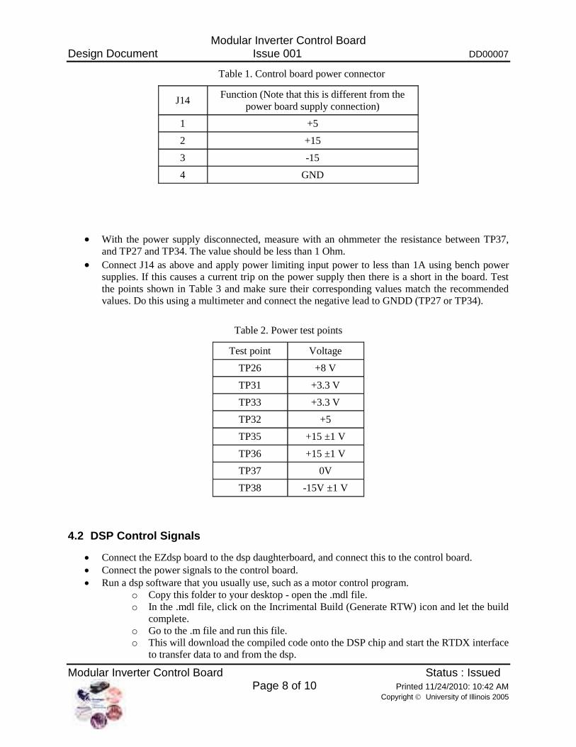
Modular Inverter Control Board Design Document Issue 001 DD00007
Modular Inverter Control Board Status : Issued Page 8 of 10 Printed 11/24/2010: 10:42 AM
Copyright University of Illinois 2005
Table 1. Control board power connector
J14 Function (Note that this is different from the
power board supply connection)
1 +5
2 +15
3 -15
4 GND
With the power supply disconnected, measure with an ohmmeter the resistance between TP37,
and TP27 and TP34. The value should be less than 1 Ohm.
Connect J14 as above and apply power limiting input power to less than 1A using bench power
supplies. If this causes a current trip on the power supply then there is a short in the board. Test
the points shown in Table 3 and make sure their corresponding values match the recommended
values. Do this using a multimeter and connect the negative lead to GNDD (TP27 or TP34).
Table 2. Power test points
Test point Voltage
TP26 +8 V
TP31 +3.3 V
TP33 +3.3 V
TP32 +5
TP35 +15 ±1 V
TP36 +15 ±1 V
TP37 0V
TP38 -15V ±1 V
4.2 DSP Control Signals
Connect the EZdsp board to the dsp daughterboard, and connect this to the control board.
Connect the power signals to the control board.
Run a dsp software that you usually use, such as a motor control program.
o Copy this folder to your desktop - open the .mdl file.
o In the .mdl file, click on the Incrimental Build (Generate RTW) icon and let the build
complete.
o Go to the .m file and run this file.
o This will download the compiled code onto the DSP chip and start the RTDX interface
to transfer data to and from the dsp.

Modular Inverter Control Board Design Document Issue 001 DD00007
Modular Inverter Control Board Status : Issued Page 9 of 10 Printed 11/24/2010: 10:42 AM
Copyright University of Illinois 2005
o When it is operating and the system is connected and on the Enable LED should light
on the power board.
This test code will allow you to control PWM signals output by the DSP and view the
corresponding Voltage and Current Outputs.
Measure the test points in Table 4. Currently only Phase A, B, and C are used.
If the output of the above test points is not working, check the test points in
Table 5 on the DSP daughter board as this is where the signals originate. If these outputs are not
present, then the program is not running on the DSP or the DSP is broken. Also check the LED
diode pack on the upper right side of the DSP daughter board to see if the LEDs are fading for the
correct channels.
Table 3. Test points for phase control signals
Test Point Function
TP5 Phase A High
TP6 Phase A Low
TP7 Phase B High
TP8 Phase B Low
TP9 Phase C High
TP10 Phase C Low
Table 4. Phase control signals
eZdsp Expansion Board P8 J5 Expansion board MV54164 D1 PWM output function
PWM7 (Pin 30) Pin 6 LED8 Phase A high
PWM8 (Pin 31) Pin 7 LED7 Phase A Low
PWM9 (Pin 32) Pin 8 LED6 Phase B high
PWM10 (Pin 33) Pin 9 LED5 Phase B low
PWM11 (Pin 34) Pin 10 LED4 Phase C high
PWM12 (Pin 35) Pin 11 LED3 Phase C low
TimerCompare LED2 Phase D High
TimerCompare LED1 Phase D low
4.3 DSP Analog Input Signals
Build an H-bridge using two phases and a power resistor in between. Use a power resistor
such that about 1 A to 3 A is flowing through the resistor for a given test power supply
voltage.

Modular Inverter Control Board Design Document Issue 001 DD00007
Modular Inverter Control Board Status : Issued Page 10 of 10 Printed 11/24/2010: 10:42 AM
Copyright University of Illinois 2005
Put jumper JP1 into position ‘Top Gate Signals’.
Connect the H-bridge between phase output A and B.
Run the VoltsperHertz test model.
The currents at each ADC input and voltages to see that they fluctuate in a sinusoidal
manner. All inputs to the ADC when Idle (Inverter is not running a load) should be
approximately 1.65V. Test the following test points for Current (Ix) and Voltage (Vx) at
connector P9 and 5 on the EZDSP board.
A 1A output draw will correspond to approximately (1/40)*1.65 + 1.65 = 1.69V at the input
pin to the DSP (Verify switching current signals with a scope to view the fast changing
transients at 10 KHz 100 μs/div).
Verify both the voltage and current signals going into the DSP. If they are not present on the
Ezdsp expansion board, verify they are present on the output of the Power board, then trace
them back through the OpAmp circuits on the control board.
Each analog current output from the power board is a differential ±15 volt signal. This is
converted to a 0 to 3.3V signal by two op amps for each channel before being sent to the
DSP.
Table 5. Analog-to-digital (ADC) assignment
ADC input EZdsp Expansion board Ezdsp Adapter pin J11 Pin Description
ADCINA0 P9 Pin 2 1 IA_LOW
ADCINA1 P9 Pin 4 3 IB_LOW
ADCINA2 P9 Pin 6 5 IC_LOW
ADCINA3 P9 Pin 8 7 ID_LOW
ADCINA4 P9 Pin 10 9 VBUS_LOW
ADCINA5 P9 Pin 12 11 T1_LOW
ADCINA6 P9 Pin 14 13 T2_LOW
ADCINA7 P9 Pin 16 15 VA_LOW
ADCINB0 P5 Pin 1 17 VB_LOW
ADCINB1 P5 Pin 2 19 VC_LOW
ADCINB2 P5 Pin 3 21 VD_LOW
ADCINB3 P5 Pin 4 23 A1_LOW
ADCINB4 P5 Pin 5 25 A2_LOW
ADCINB5 P5 Pin 6 27 A3_LOW
ADCINB6 P5 Pin 7 29 A4_LOW
ADCINB7 P5 Pin 8 31 B1_LOW
Grainger Center for Electric Machinery and Electromechanics Department of Electrical and Computer Engineering
University of Illinois at Urbana-Champaign 1406 W. Green St.
Urbana, IL 61801
The information contained in this Document and the Appendices may not be copied, reproduced, distributed or stored in a retrieval system without the prior express written permission of the author.
Copyright Board of Trustees of the University of Illinois 2005. All Rights Reserved
Design Document
Analog PWM Daughterboard
Reference: DD00008
Issue: 001
Status: Issued
Author: Zakdy Sorchini
Principal Investigator: Jonathan Kimball
Created: March 6, 2006
\\ece-powernts2\ece power design archives\documents\design documents\dd00008-001 analog pwm daughterboard.doc
Abstract:
This document briefly describes the functionality and characteristics of the analog PWM
daughterboard for the modular inverter. Sine-triangle PWM is implemented.
Analog PWM Daughterboard Design Document Issue 001 DD00008
Analog PWM Daughterboard Status : Issued Page 2 of 5 Printed 11/24/2010: 10:43 AM
Copyright University of Illinois 2005
Document Revision History
Issue Date Comments
000 6/27/2005 Initial release. 001 3/6/2006 Added a reference to the control board CPLD software.
Contents
1. Introduction ......................................................................................................... 3
1.1 Scope ..................................................................................................................................... 3
1.2 References ............................................................................................................................. 3
1.3 Known Issues ......................................................................................................................... 3
2. Interface .............................................................................................................. 3
2.1 Power ..................................................................................................................................... 3
2.2 Analog Signals ....................................................................................................................... 3
2.3 Digital Signals ........................................................................................................................ 3
3. Timming .............................................................................................................. 4
3.1 Triangle waveform .................................................................................................................. 4
3.2 PWM Clock............................................................................................................................. 4
4. PWM Channels ................................................................................................... 4
5. Over-current Protection....................................................................................... 4

Analog PWM Daughterboard Design Document Issue 001 DD00008
Analog PWM Daughterboard Status : Issued Page 3 of 5 Printed 11/24/2010: 10:43 AM
Copyright University of Illinois 2005
1. Introduction
The analog PWM daughterboard is one of the control modules for the modular inverter. It provides
four sine-triangle PWM channels with pulse-by-pulse over-current protection. The triangular
waveform is obtained from a discrete IC to have better stability and linearity.
1.1 Scope
The analog PWM daughterboard is intended to be used as part of the modular inverter, together
with the control board. Primary use is for research.
The over-current functionality is only available when the control board CPLD is programmed to
synchronize the over-current signal with the PWM clock. The signal cannot be used directly to
disable transistors.
1.2 References
Schematic: SK0048 rev 1
Layout: PB0048 rev A
Control board: SK0038 and PB0038
CPLD software for Control Board: SW0018
1.3 Known Issues
The over-current protection circuits are active high, must be active low for the wired-OR
configuration to work. Just reverse all the input signals (not the positive feedback) to the
comparators (U1, U3, U4 and U5) by cutting traces and reconnecting.
2. Interface
2.1 Power
The analog PWM daughterboard requires ±15 V, ±12 V, 5 V and 3.3 V. The ±12 V supply is used
by the triangle waveform generator and is created from the ±15 V supply using zener diodes. The
logic voltage is either 5 V or 3.3 V, selected via jumper JP1.
2.2 Analog Signals
The daughterboard uses the high voltage analog connector. The signals used are the currents (pins
1, 3, 5 and 7) and the modulating signals (pins 23, 25, 27 and 29). The current signals must be
preferentially unfiltered for the pulse-by-pulse over-current protection to work properly. All signals
can be up to ±15 V, but the range used is ±10 V (the carrier is set for this last range).
2.3 Digital Signals

Analog PWM Daughterboard Design Document Issue 001 DD00008
Analog PWM Daughterboard Status : Issued Page 4 of 5 Printed 11/24/2010: 10:43 AM
Copyright University of Illinois 2005
Only the primary digital connector is used. The PWM signals are available on pins 1-4, the over-
current signal on pin 5 and the PWM clock on pin 6. All digital signals can be in the range of 0 to 5
V.
3. Timing
3.1 Triangle waveform
An LM565 (phase lock loop IC) is used as the triangle waveform source. The IC requires ±12 V
which is made available from Zener regulators. The frequency of oscillation is adjustable via an
external panel-mounted pot (20 k) and a timing capacitor (selected via jumper J5). The frequency is
adjustable from 200 Hz up to 100 kHz. (A particular capacitor setting allows a change in frequency
of roughly one decade.)
The stability of the frequency and the linearity of the waveform were significantly better than a
discrete implementation of a triangle waveform oscillator.
The signal on the LM565 has a dc offset, so the signal is buffered and then AC coupled to an
amplifier stage to set the amplitude of the triangle to ±10 V.
3.2 PWM Clock
The LM565 IC also provides a clock signal synchronized with the triangle waveform (pin 4), but
has zero dc offset. A comparator is used to make the signal TTL compatible. Resistors R54 and
R56 are typically not required.
4. PWM Channels
The implemented PWM is sine-triangle PWM. The PWM signals are obtained by comparing the
(buffered) modulating signals with the triangle waveform. Small positive feedback is used to avoid
false pulses at the output of the comparator. Signal level is 0 to 5 V or 0 to 3.3 V, depending on the
selected voltage.
5. Over-current Protection
Pulse-by-pulse over-current protection is implemented in a per-channel basis, but with only a single
over-current signal (flag) available. The over-current signal is intended to directly control the
enable of the power stage, after synchronizing it with the PWM clock (this is done in the control
board CPLD).
The current signal is rectified (the diode drop is not critical since only the peak of the current
waveform is of interest) and compared to an adjustable trip voltage. The current signal goes first
through a first order passive low pass filter, and then fed to both positive and negative half-wave
rectifiers. The resulting signals are then fed to the positive and negative pins of the comparator. The
trip voltage is fed to the negative pin and the positive is connected to an additional balancing
resistor network, with a pot (R8, R16, R29 and R37). The potentiometer must be adjusted to ensure
symmetric over-current detection (i.e., adjust until the over-current signal is active at the same level
on both the positive and negative cycle).

Analog PWM Daughterboard Design Document Issue 001 DD00008
Analog PWM Daughterboard Status : Issued Page 5 of 5 Printed 11/24/2010: 10:43 AM
Copyright University of Illinois 2005
All the over-current channels are in a wired-OR configuration to create the over-current signal the
goes to the control board. This signal cannot be used directly to control the ENABLE of the power
stage, since it is not synchronized to the PWM clock.
Within the control board CPLD, a D type flip-flop must be used with a 1 on the input, the PWM
clock as the clock input and the over-current signal connected to the asynchronous clear. The
output of the flip-flop directly controls the enable. This disables the gates as long as the over-
current condition is present, but only allows the gates to be enabled in synch with the PWM clock,
i.e., the gates can only be enabled every PWM cycle.
6. Control Board CPLD
The software for the control board CPLD can be found in the Power Design Archives under
Software as SW0018.

Grainger Center for Electric Machinery and Electromechanics Department of Electrical and Computer Engineering
University of Illinois at Urbana-Champaign 1406 W. Green St.
Urbana, IL 61801
The information contained in this Document and the Appendices may not be copied, reproduced, distributed or stored in a retrieval system without the prior express written permission of the author.
Copyright Board of Trustees of the University of Illinois 2005. All Rights Reserved
Design Document
eZDSP TMS320F2812 DSP Daughterboard
Reference: DD00009
Issue: 000
Status: Issued
Author: J. Wells / Z. Sorchini
Principal Investigator: Jonathan Kimball
Created: July 5, 2005
\\ece-powernts2\ece power design archives\documents\design documents\dd00009-000 ezdsp tms320f2812 dsp daughterboard.doc
Abstract:
This document briefly describes the functionality and characteristics of the eZDSP TMS320F2812
DSP daughter board. Additionally, several useful documents are referenced which can aid the new
user in understanding how to make the most of the available functionality.
eZDSP TMS320F2812 DSP Daughterboard Design Document Issue 000 DD00009
eZDSP TMS320F2812 DSP Daughterboard Status : Issued Page 2 of 4 Printed 11/24/2010: 10:43 AM
Copyright University of Illinois 2005
Document Revision History
Issue Date Comments
000 3/8/2006 Initial release.
Contents
1. Introduction ......................................................................................................... 3
1.1 Scope ..................................................................................................................................... 3
1.2 References ............................................................................................................................. 3
1.3 Known Issues/Suggested Revisions ...................................................................................... 3
2. Interface .............................................................................................................. 4
2.1 Control Board Interface .......................................................................................................... 4
2.1.1 Power ................................................................................................................................ 4
2.1.2 Analog Signals .................................................................................................................. 4
2.1.3 Digital Signals ................................................................................................................... 4
2.2 Daughterboard External Connectors ..................................................................................... 4
2.2.1 Communications ............................................................................................................... 4
2.2.2 Filtered Analog Outputs .................................................................................................... 4
2.2.3 Digital I/O .......................................................................................................................... 4

eZDSP TMS320F2812 DSP Daughterboard Design Document Issue 000 DD00009
eZDSP TMS320F2812 DSP Daughterboard Status : Issued Page 3 of 4 Printed 11/24/2010: 10:43 AM
Copyright University of Illinois 2005
1. Introduction
The eZDSP TMS320F2812 DSP daughterboard is one of the control modules for the modular
inverter. The board provides peripheral circuitry needed to take advantage of many of the
functionalities of the TMS320F2812 core. Extensive information regarding the capabilities of the
DSP core can be found at:
http://focus.ti.com/docs/prod/folders/print/tms320f2812.html
1.1 Scope
The eZDSP TMS320F2812 DSP daughterboard is primarily intended to be used as part of the
modular inverter, together with the control board. Primary use is for research. It should be noted
that the board can be used as a stand alone board to develop code for the DSP as well.
1.2 References
Schematic: SK0048
Layout: PB0048
Control board: SK0038 and PB0038
CPLD software for Control Board: SW0026
Guide to Programming the eZDSP TMS320F2812 DSP through Matlab: TU00003
1.3 Known Issues/Suggested Revisions
10 Pin serial headers (J13, J14) should be fixed such that the pin connections match
correctly with a standard serial connector.
Resistor R2 should be changed to 470 ohms to provide ample current to drive the LED
bank.
Matlab does not appear to support pin level input/output configuration. It appears that such
configuration is done at the port level. As such, when using Matlab, only the input switches
(SW1) or the output LEDs (D1) can be used at a given time.
The next revision of the board should improve the label layout on the physical board for
easier reading.
The physical position of connectors J17 and J18 should be swapped in a future revision.
A possible addition to the next revision would be to include an improved 16 bit A/D chip
as detailed in:
http://focus.ti.com/docs/apps/catalog/resources/appnoteabstract.jhtml?abstractName=slaa1
67.
A possible addition to the next revision would be to include an actual D/A chip which
could be operated using the SPI bus of the DSP. See Application Note:
http://focus.ti.com/docs/apps/catalog/resources/appnoteabstract.jhtml?abstractName=slaa1
76.

eZDSP TMS320F2812 DSP Daughterboard Design Document Issue 000 DD00009
eZDSP TMS320F2812 DSP Daughterboard Status : Issued Page 4 of 4 Printed 11/24/2010: 10:43 AM
Copyright University of Illinois 2005
2. Interface
2.1 Control Board Interface
2.1.1 Power
The eZDSP TMS320F2812 DSP Daughterboard requires ±15 V, 5 V and 3.3 V as supplied by the
Control Board referenced in SK0038. If desired, the board can be run as a stand alone device by
powering the eZDSP using the 5 V power supply provided by Spectrum Digital
(www.spectrumdigital.com)
2.1.2 Analog Signals
The daughterboard uses the low voltage analog connector. DO NOT connect analog signals outside
the 0-3 V range as this may cause damage to the DSP core. All analog signals are passed through a
first order low pass filter. Note that the cutoff frequency was intended to be chosen by the user and
may vary from board to board.
2.1.3 Digital Signals
Both the primary digital and secondary digital connectors are used to route signals to the control
board. All digital signals are TTL compatible 3.3 V CMOS and are NOT 5 V tolerant.
2.2 Daughterboard External Connectors
2.2.1 Communications
SCI communications are available through connectors J13 and J14. SPI communications are
available through connector J13. A CAN interface is available through connector J6. An RS-232
(serial port) communication channel is available through connector J7.
2.2.2 Filtered Analog Outputs
Four PWM channels (PWM1, PWM3, PWM5 and T1PWM/T1CMP) are available to be used as
D/A converters. The PWM signals are filtered with 4th-order low pass filters (Sallen Key
implementation). Each channel can be connected to the filter with a dedicated jumper such that, if
required, the digital PWM signals can be used directly. The analog signals are available in
connectors J15-J18. The signal range is ±10 V.
2.2.3 Digital I/O
A generic digital input DIP switch (SW1) is available with 8 lines. Three toggle switches (S1-S3)
are available, which can also be controlled with an external switch (J8-J10). Eight digital outputs
are available visually on LEDs (D1). Refer to SK0048 for the specific DSP pins connected to each
digital line. Assume all signals are in the 0 to 3.3 V range.

Grainger Center for Electric Machinery and Electromechanics Department of Electrical and Computer Engineering
University of Illinois at Urbana-Champaign 1406 W. Green St.
Urbana, IL 61801
The information contained in this Document and the Appendices may not be copied, reproduced, distributed or stored in a retrieval system without the prior express written permission of the author.
Copyright Board of Trustees of the University of Illinois 2008. All Rights Reserved
Design Document
Firefly II FPGA Daughterboard
Reference: DD000013
Issue: 001
Status: Issued
Author: Amrit R Iyer
Updated By: Paul Rancuret / Jim Kolodziej
Principal Investigator: Jonathan Kimball
Created: June 20, 2008
Updated: November 23, 2010
\\ece-serv-08\power\designarchives\documents\design documents\dd00013-000 fpga daughtercard.doc
Abstract:
This document outlines the design of Firefly II FPGA daughterboard for the modular inverter
project. The objective of the project and current progress are briefly discussed, and an in depth look
of the hardware selection and PCB layout is given. A brief programming tutorial is also provided at
the end of the document.

Firefly II FPGA Daughterboard Design Document Issue 001 DD000013
Firefly II FPGA Daughterboard Status : Issued Page 2 of 26 Printed 11/24/2010: 10:46 AM
Copyright University of Illinois 2008
Document Revision History
Issue Date Comments
000 6/20/2008 Initial release. 001 11/23/2010 Updated Interface Issues with Modular Inverter
Contents
1. Introduction ......................................................................................................... 4
1.1 Scope ..................................................................................................................................... 4
1.2 References ............................................................................................................................. 4
1.3 Known Issues/Suggested Revisions ...................................................................................... 5
2. Interface .............................................................................................................. 5
2.1 Control Board Interface .......................................................................................................... 5
2.1.1 Power ................................................................................................................................ 5
2.1.2 Analog Signals .................................................................................................................. 5
2.1.3 Digital Signals ................................................................................................................... 5
2.2 Daughterboard External Connectors ..................................................................................... 5
2.2.1 Communications ............................................................................................................... 6
2.2.2 Analog Outputs ................................................................................................................. 6
2.2.3 Digital I/O .......................................................................................................................... 7
2.3 Known Interface Issues .......................................................................................................... 7
2.3.1 Physical Interface .............................................................................................................. 7
2.3.2 Control Board/Daughterboard Digital IO Pinout Errors ..................................................... 7
2.4 Interface Issues for V/Hz Control ........................................................................................... 8
2.4.1 DSP Builder Model ............................................................................................................ 9
2.4.2 Generating a Sinusoid ...................................................................................................... 9
2.4.3 Implementing the Control ................................................................................................ 10
3. PCB Design ...................................................................................................... 10
3.1 Part Values ........................................................................................................................... 10
3.2 Layout Considerations ......................................................................................................... 14
3.3 Wires and Vias ..................................................................................................................... 14
3.4 Layers ................................................................................................................................... 14
3.5 Test Points ........................................................................................................................... 14
4. Components ..................................................................................................... 15
4.1 Firefly II Module .................................................................................................................... 15
4.2 1.2-V Regulator .................................................................................................................... 17
4.3 Analog to Digital Converters ................................................................................................ 17

Firefly II FPGA Daughterboard Design Document Issue 001 DD000013
Firefly II FPGA Daughterboard Status : Issued Page 3 of 26 Printed 11/24/2010: 10:46 AM
Copyright University of Illinois 2008
4.4 Digital to Analog Converters ................................................................................................ 17
4.5 Differential Amplifiers ........................................................................................................... 17
4.6 EEPROM .............................................................................................................................. 17
4.7 CPLD .................................................................................................................................... 18
5. Progress ........................................................................................................... 19
6. FPGA Daughterboard Nios II Programming Tutorial ......................................... 19

Firefly II FPGA Daughterboard Design Document Issue 001 DD000013
Firefly II FPGA Daughterboard Status : Issued Page 4 of 26 Printed 11/24/2010: 10:46 AM
Copyright University of Illinois 2008
1. Introduction
The purpose of the FPGA daughterboard is to provide a plug alternative to the DSP daughterboard
used for the control of the modular inverter. Moving from a DSP chip to an FPGA will allow for
increased flexibility and speed.
The Firefly II Module built by Microtronix utilizes an Altera Cyclone II FPGA along with some
peripheral circuitry. This module was chosen over a stand alone FPGA due to the convenience of
its 144-pin package, which is much easier to work with than the BGA packages that most FPGA
chips are available in.
1.1 Scope
The FPGA daughterboard is primarily intended to be used as part of the modular inverter, together
with the control board. Primary use is for research. It should be noted that the board can be used as
a stand alone board to develop code for a variety of other applications as well.
1.2 References
FPGA daughterboard schematic: PCB50021
\\ece-serv-08\Power\DesignArchives\PCBs\EAGLE Designs\PCB50021\Rev
A\pcb50021_a_final.sch
FPGA daughterboard layout: PCB50021
\\ece-serv-08\Power\DesignArchives\PCBs\EAGLE Designs\PCB50021\Rev
A\pcb50021_a_final.brd
SSD board schematic: PCB50022
\\ece-serv-08\Power\DesignArchives\PCBs\EAGLE Designs\PCB50022\Rev A\pcb50022_a.sch
Control board schematic: SK0038
\\ece-serv-08\Power\DesignArchives\PCBs\Schematics\SK0038\Rev 2\sk0038_2.opj
Control board layout: PB0038
\\ece-serv-08\Power\DesignArchives\PCBs\Layouts\PB0038\Rev B\pb0038_B.max
CPLD software for control board: SW0026
\\ece-serv-08\Power\DesignArchives\Software\SW0026\Rev B\
VHDL software for FPGA daughterboard CPLD:
\\ece-serv-08\Power\DesignArchives\Software\SW0045
VHDL software for FPGA software:
\\ece-serv-08\Power\DesignArchives\Software\SW0044
Nios II software for FPGA software:
\\ece-serv-08\Power\DesignArchives\Software\SW0044

Firefly II FPGA Daughterboard Design Document Issue 001 DD000013
Firefly II FPGA Daughterboard Status : Issued Page 5 of 26 Printed 11/24/2010: 10:46 AM
Copyright University of Illinois 2008
1.3 Known Issues/Suggested Revisions
In the library for rev A, the package for the LTC2620 part should be a narrow SSOP-16
instead of a SSOP-16. This error is corrected in rev B.
In the library for rev A, pins 1 and 3 for the D2PAK-3 package are swapped. These pins
need to be switched when soldering the 1.2-V regulator, U17, onto the daughterboard. This
error is corrected in rev B.
Headers J3 and J4 on the daughterboard incorrectly interface with headers J5 and J2 on the
modular inverter control board. See section 2.3 for more details. A further revision of the
board layout to correct this is recommended.
Header J1 on the daughterboard incorrectly switches the ±15-V pins with respect to those
on the modular inverter control board. A further revision of the board layout to correct this
is recommended.
2. Interface
2.1 Control Board Interface
2.1.1 Power
The FPGA daughterboard requires ±15-V, 5-V, and 3.3-V, which are provide via connecter J1 on
the daughterboard. This connector is designed to interface with J12 on the main control board,
which is referenced in SK0038 of section 1.2. A 1.2-V supply is also needed to power the Cyclone
II FPGA, and this is provided on the daughterboard by a linear regulator fed from the 3.3-V line
provided by J1.
Note that the ±15-V pins on J1 are switched with respect to the pin connections on the modular
inverter control board. However, this power source may be unnecessary if the Digital to Analog
outputs on the daughterboard are not used. A further revision of the board layout to correct this is
recommended.
2.1.2 Analog Signals
The daughterboard uses the low voltage analog connector J15 on the main control board. This
connector is designed to hook to J2 on the daughterboard and provides analog signals ranging from
0 to 3-V. Voltage levels larger than 5.25-V will damage the ADCs used on the FPGA
daughterboard.
2.1.3 Digital Signals
Connectors J2 and J5 on the main control board are used to route digital signals to FPGA
daughterboard via connectors J4 and J3 on the main control board. All digital signals are TTL
compatible 3.3-V CMOS.
2.2 Daughterboard External Connectors

Firefly II FPGA Daughterboard Design Document Issue 001 DD000013
Firefly II FPGA Daughterboard Status : Issued Page 6 of 26 Printed 11/24/2010: 10:46 AM
Copyright University of Illinois 2008
2.2.1 Communications
A JTAG interface is available through connector J5, for use with Altera’s USB Blaster and
Byteblaster II cables. An RS-232 (serial port) communication channel is available through
connector J6.
2.2.2 Analog Outputs
An 8-channel DAC along with an array of differential amplifiers provide ±10-V analog outputs via
connector J10.
Firefly II FPGA Daughterboard Design Document Issue 001 DD000013
Firefly II FPGA Daughterboard Status : Issued Page 7 of 26 Printed 11/24/2010: 10:46 AM
Copyright University of Illinois 2008
2.2.3 Digital I/O
An 8 input DIP switch, three pushbutton switches, and a 10-segment LED display are available to
the FPGA via the daughterboard’s CPLD. Connector J7 provides access to an Optrex LCD module
which can be seen at:
http://dekiwiki.ece.uiuc.edu/@api/deki/files/22/=LCDModule_DMC-16204NY-LY.pdf
Connector J9 provide access to the SSD board referenced in PCB50022 of section 1.2.
Table 1: Summary of FPGA Daughterboard Connectors
J Description
1 Power routing from J3 on the main control board
2 Low voltage analog input from J15 on the main control board
3 Digital IO from J5 on the main control board
4 Digital IO from J2 on the main control board
5 Header for Altera Byteblaster II cable, used for Firefly II's JTAG communications
6 Female DB-9 header, used for Firefly II's RS232 communications
7 Connector to LCD module
8 Header for Xilinx Parallel IV cable, used for CPLD's JTAG communications
9 Connector to SSD board
10 ±10-V analog output from DAC
2.3 Known Interface Issues
The following information documents some of the progress that has been made toward
interfacing the Firefly II FPGA daughterboard with the control board for the modular inverter,
and issues that were found.
2.3.1 Physical Interface
One of the first steps was determining the physical connections that would need to be made
between the FPGA daughterboard and the control board. There were 4 sets of pin headers on the
bottom of the daughterboard that provide power and data transfer. Each of these headers needed
to be de-soldered because they were not long enough to plug into the control board. All of the
headers on the bottom were replaced with longer ones.
2.3.2 Control Board/Daughterboard Digital IO Pinout Errors
Closer examination of headers J3 and J4 on the daughterboard revealed incorrect interfacing with
control board headers J5 and J2, respectively. On the control board, J5 pins 15/16 and J2 pins
19/20 were connected to ground. Similarly on the daughterboard, J3 pins 15/16 and J4 pins 19/20
were connected to ground. However, these pin numbers were NOT physically lined up correctly
because the headers were reversed when laid out on the daughterboard. Table 2 below illustrates
this. (Note the power and analog connectors both were correctly matched in terms of pin number)
Firefly II FPGA Daughterboard Design Document Issue 001 DD000013
Firefly II FPGA Daughterboard Status : Issued Page 8 of 26 Printed 11/24/2010: 10:46 AM
Copyright University of Illinois 2008
Table 2: Daughterboard Connectors J3 and J4 errors
J3-Daughterboard
J5 – Control Board
| J4-Daughterboard
J2 – Control Board
Pin 1 Pin 16 | Pin 1 Pin 20
Pin 2 Pin 15 | Pin 2 Pin 19
Pin 3 Pin 14 | Pin 3 Pin 18
… … | … …
Pin 14 Pin 3 | Pin 18 Pin 3
Pin 15 Pin 2 | Pin 19 Pin 2
Pin 16 Pin1 | Pin 20 Pin1
Ramifications:
There were a few issues that arose with incorrect pin layout.
1) The first two pins on J3 and J4 were FPGA IO pins on the FPGA, but these were both
connected to ground on the control board.
2) The first two pins on J5 and J2 were digital IO pins on the control board CPLD, but these
were both connected to the daughterboard ground ( same as the control board ground)
3) Since there were a number of pin numbers reversed, there were less digital IO lines of
communication between the control board and the daughterboard.
4) The chance for error was greater when determining which control board IO signals
corresponded to the daughterboard IO signals.
The board should still be able to function correctly since all of the IO pins that are pulled to
ground essentially “see” low inputs. However, due to the reasons listed above it would be
desirable to make the necessary corrections to align these pins for future daughterboard revisions.
2.4 Interface Issues for V/Hz Control
This section outlines the steps that were taken to allow for basic V/Hz control.
At this time there was not an attempt made to receive any analog feedback from the control board
(voltages, currents, etc). In order to implement a basic V/Hz control there were four digital IO
channels between the FPGA and the control board CPLD that needed to be configured. More
specifically, three channels were needed for the A, B, and C phase PWM signals and a fourth
channel was needed for a clock signal. The clock signal was needed to let the CPLD know the
FPGA was running in order to allow the enable signal to be generated.
Table 3 below lists the signal flow to help with interfacing the daughterboard to the control board
of the modular inverter. The CPLD that was used contained the code for the current DSP
interface (SW0029)

Firefly II FPGA Daughterboard Design Document Issue 001 DD000013
Firefly II FPGA Daughterboard Status : Issued Page 9 of 26 Printed 11/24/2010: 10:46 AM
Copyright University of Illinois 2008
Table 3: CPLD Output Pin Assignments for V/Hz Control
CPLD Signal CPLD Pin Assignme
nt
Control Board Signal
Control Board
Header
Daughterboard FPGA Header
FPGA Pin Assignme
nt
T4PWM-T4CMP P25 GIO_19 J5 - #3 J3 - #14 AB19
PWM7 (Phase A) P32 GIO_22 J5 - #6 J3 - #11 AA19
PWM9 (Phase B) P34 GIO_24 J5 - #8 J3 - #9 AB17
PWM11 (Phase C) P36 GIO_26 J5 - #10 J3 - #7 AB16
2.4.1 DSP Builder Model
In order to program the FPGA, Simulink (in conjunction with DSP builder) was used to build the
model, compile the design, and program the device. More information on using DSP builder can
be found by accessing the DSP user guide
http://www.altera.com/literature/ug/ug_dsp_builder.pdf. Furthermore, specific information for the
daughterboard custom components and board support can be found in the document “DSP
Builder FPGA documentation”.
2.4.2 Generating a Sinusoid
In order to generate a sinusoidal waveform on the FPGA, the megacore function “NCO_v9”
found in the Simulink library “Altera DSP Builder Blockset” was used. Detailed documentation
on the NCO (numerically controlled oscillator) can be found at
http://www.altera.com/literature/ug/ug_nco.pdf.
Once the NCO was added to the model, double clicking on the block would allow for it to be
parameterized. The following parameters are used to configure the NCO:
Parameters Tab:
1) Phase Accumulator Precision – 32bits
2) Angular Resolution – 16bits
3) Phase Magnitude Precision – 11 bits (specifies the magnitude of the waveform as a
signed int)
4) Clock Rate – 24MHz (this is the speed of the Firefly II FPGA clock)
5) Desired Output Frequency - 60Hz
The calculated phase increment value that is displayed is used set the output frequency.
This value needs to be input as 32 bit constant integer to the block’s “phi_inc” input.
Implementation Tab:
1) Phase Modulation Input – enabled with 16 bit precision
2) Outputs – single output (for generating sine wave)
3) Device Family – Cyclone II
Once the block is properly configured, it can be generated. In addition to the “phi_inc” input
already described, the block takes and active low reset input and an active high enable input. The
“phase_mod” input specifies the phase shift of the waveform and ranges from 0 to 2pi over a

Firefly II FPGA Daughterboard Design Document Issue 001 DD000013
Firefly II FPGA Daughterboard Status : Issued Page 10 of 26 Printed 11/24/2010: 10:46 AM
Copyright University of Illinois 2008
16bit integer. Therefore a 120 degree phase shift would require a 16 bit integer constant equal to
2^16*(1/3).
2.4.3 Implementing the Control
The NCO output sinusoid is represented as a signed 11 bit integer. In order to make this number
unsigned for easy integration with the rest of the Altera DSP builder blocks, the number 2 ^ (n-1)
-1 is added (where “n” is the number of bits of the signed 2’s complement number being
converted to an unsigned number). This 11 bit unsigned number is then made into a 12 bit
number and a constant 2^10 is added to it. This is done in order to make the sinusoid minimum
and maximum oscillate between 25% and 75% of the range of the 12 bit number.
Finally, this 12 bit number is compared to an incrementing 12 bit number in order to generate a
PWM signal. The frequency of the PWM is calculated by dividing the clock frequency of the
FPGA by the number of bits in the counter: 24MHz/2^12 bits ~ 5.895kHz
Additionally a simple block created in VHDL is used to produce a 1.2MHz ”heartbeat” signal to
let the CPLD know that the FPGA is running and that the enable signal should be generated.
3. PCB Design
3.1 Part Values
The EAGLE schematic and layout can be found in the PCB50021 file referenced in section 1.2. Pdf
versions of these files can also be found at:
http://dekiwiki.ece.uiuc.edu/@api/deki/files/56/=sch50021_a_final.pdf
http://dekiwiki.ece.uiuc.edu/@api/deki/files/55/=pcb50021_a_final.pdf
Table 4, Table 5, and Table 6 shown on the next three pages give descriptions and values for the
various IC’s, resistors, and capacitors.
Firefly II FPGA Daughterboard Design Document Issue 001 DD000013
Firefly II FPGA Daughterboard Status : Issued Page 11 of 26 Printed 11/24/2010: 10:46 AM
Copyright University of Illinois 2008
Table 4: IC Part Numbers and Descriptions
U Description IC part number
1 ADC1 AD7476
2 ADC2 AD7476
3 ADC3 AD7476
4 ADC4 AD7476
5 ADC5 AD7476
6 ADC6 AD7476
7 ADC7 AD7476
8 ADC8 AD7476
9 ADC9 AD7476
10 ADC10 AD7476
11 ADC11 AD7476
12 ADC12 AD7476
13 ADC13 AD7476
14 ADC14 AD7476
15 ADC15 AD7476
16 ADC16 AD7476
17 1.2 V regulator NCP565 NCP565
18 Firefly II module Firefly II
19 CPLD XC9572
20 DAC x8 LTC2620
21 EEPROM AT25256
22 LED x10 HDSP-4830
23 DIP Switch x10 76SB08T
24 Op Amp 1 TL082
25 Op Amp 2 TL082
26 Op Amp 3 TL082
27 Op Amp 4 TL082
28 Switch 1 PST645
29 Switch 2 PST646
30 Switch 3 PST647
Firefly II FPGA Daughterboard Design Document Issue 001 DD000013
Firefly II FPGA Daughterboard Status : Issued Page 12 of 26 Printed 11/24/2010: 10:46 AM
Copyright University of Illinois 2008
Table 5: Resistor Values and Purposes
R Value (kΩ) Description R Value (kΩ) Description
1 0.06 Pull up resistor for LED 1 49 1 digital input protection, J3, pin 3
2 0.06 Pull up resistor for LED 2 50 1 digital input protection, J3, pin 4
3 0.06 Pull up resistor for LED 3 51 1 digital input protection, J3, pin 5
4 0.06 Pull up resistor for LED 4 52 1 digital input protection, J3, pin 6
5 0.06 Pull up resistor for LED 5 53 1 digital input protection, J3, pin 7
6 0.06 Pull up resistor for LED 6 54 1 digital input protection, J3, pin 8
7 0.06 Pull up resistor for LED 7 55 1 digital input protection, J3, pin 9
8 0.06 Pull up resistor for LED 8 56 1 digital input protection, J3, pin 10
9 0.06 Pull up resistor for LED 9 57 1 digital input protection, J3, pin 11
10 0.06 Pull up resistor for LED 10 58 1 digital input protection, J3, pin 12
11 24 Level Shifter A 59 1 digital input protection, J3, pin 13
12 12.96 Level Shifter A 60 1 digital input protection, J3, pin 14
13 1.2 Level Shifter A 61 1 digital input protection, J4, pin 1
14 10 Level Shifter A 62 1 digital input protection, J4, pin 2
15 24 Level Shifter B 63 1 digital input protection, J4, pin 3
16 12.96 Level Shifter B 64 1 digital input protection, J4, pin 4
17 1.2 Level Shifter B 65 1 digital input protection, J4, pin 5
18 10 Level Shifter B 66 1 digital input protection, J4, pin 6
19 24 Level Shifter C 67 1 digital input protection, J4, pin 7
20 12.96 Level Shifter C 68 1 digital input protection, J4, pin 8
21 1.2 Level Shifter C 69 1 digital input protection, J4, pin 9
22 10 Level Shifter C 70 1 digital input protection, J4, pin 10
23 24 Level Shifter D 71 1 digital input protection, J4, pin 11
24 12.96 Level Shifter D 72 1 digital input protection, J4, pin 12
25 1.2 Level Shifter D 73 1 digital input protection, J4, pin 13
26 10 Level Shifter D 74 1 digital input protection, J4, pin 14
27 24 Level Shifter E 75 1 digital input protection, J4, pin 15
28 12.96 Level Shifter E 76 1 digital input protection, J4, pin 16
29 1.2 Level Shifter E 77 1 digital input protection, J4, pin 17
30 10 Level Shifter E 78 1 digital input protection, J4, pin 18
31 24 Level Shifter F 79 1 digital input protection, J4, pin 19
32 12.96 Level Shifter F 80 1 analog input protection for ADC 1
33 1.2 Level Shifter F 81 1 analog input protection for ADC 2
34 10 Level Shifter F 82 1 analog input protection for ADC 3
35 24 Level Shifter G 83 1 analog input protection for ADC 4
36 12.96 Level Shifter G 84 1 analog input protection for ADC 5
37 1.2 Level Shifter G 85 1 analog input protection for ADC 6
38 10 Level Shifter G 86 1 analog input protection for ADC 7
39 24 Level Shifter H 87 1 analog input protection for ADC 8
40 12.96 Level Shifter H 88 1 analog input protection for ADC 9
41 1.2 Level Shifter H 89 1 analog input protection for ADC 10
42 10 Level Shifter H 90 1 analog input protection for ADC 11
43 10 (potentiometer) Contrast adjustment for LCD Module 91 1 analog input protection for ADC 12
44 0 analog ground jumper 92 1 analog input protection for ADC 13
45 0 digital ground jumper 93 1 analog input protection for ADC 14
46 10 (potentiometer) Backlight brightness for LCD Module 94 1 analog input protection for ADC 15
47 1 digital input protection, J3, pin 1 95 1 analog input protection for ADC 16
48 1 digital input protection, J3, pin 2

Firefly II FPGA Daughterboard Design Document Issue 001 DD000013
Firefly II FPGA Daughterboard Status : Issued Page 13 of 26 Printed 11/24/2010: 10:46 AM
Copyright University of Illinois 2008
Table 6: Capacitor Values, Packages, and Purposes
C Value Description Type
1 22 µF Power bus decoupling, 3.3V Electrolytic
2 22 µF Power bus decoupling, 5V Electrolytic
3 22 µF Power bus decoupling,+15V Electrolytic
4 22 µF Power bus decoupling, -15V Electrolytic
5 0.1 µF Decoupling for ADC1 MLCC_0805
6 0.1 µF Decoupling for ADC2 MLCC_0805
7 0.1 µF Decoupling for ADC3 MLCC_0805
8 0.1 µF Decoupling for ADC4 MLCC_0805
9 0.1 µF Decoupling for ADC5 MLCC_0805
10 0.1 µF Decoupling for ADC6 MLCC_0805
11 0.1 µF Decoupling for ADC7 MLCC_0805
12 0.1 µF Decoupling for ADC8 MLCC_0805
13 0.1 µF Decoupling for ADC9 MLCC_0805
14 0.1 µF Decoupling for ADC10 MLCC_0805
15 0.1 µF Decoupling for ADC11 MLCC_0805
16 0.1 µF Decoupling for ADC12 MLCC_0805
17 0.1 µF Decoupling for ADC13 MLCC_0805
18 0.1 µF Decoupling for ADC14 MLCC_0805
19 0.1 µF Decoupling for ADC15 MLCC_0805
20 0.1 µF Decoupling for ADC16 MLCC_0805
21 0.1 µF Decoupling for CPLD MLCC_0805
22 0.1 µF Decoupling for CPLD MLCC_0805
23 0.1 µF Decoupling for DACs MLCC_0805
24 0.1 µF Decoupling for EEPROM MLCC_0805
25 0.1 µF Decoupling for Op Amp 1 MLCC_0805
26 0.1 µF Decoupling for Op Amp 1 MLCC_0805
27 0.1 µF Decoupling for Op Amp 2 MLCC_0805
28 0.1 µF Decoupling for Op Amp 2 MLCC_0805
29 0.1 µF Decoupling for Op Amp 3 MLCC_0805
30 0.1 µF Decoupling for Op Amp 3 MLCC_0805
31 0.1 µF Decoupling for Op Amp 4 MLCC_0805
32 0.1 µF Decoupling for Op Amp 4 MLCC_0805
33 0 µF Filtering Capacitor for level shifting monolithic
34 0 µF Filtering Capacitor for level shifting monolithic
35 0 µF Filtering Capacitor for level shifting monolithic
36 0 µF Filtering Capacitor for level shifting monolithic
37 0 µF Filtering Capacitor for level shifting monolithic
38 0 µF Filtering Capacitor for level shifting monolithic
39 0 µF Filtering Capacitor for level shifting monolithic
40 0 µF Filtering Capacitor for level shifting monolithic
41 0 µF Filtering Capacitor for level shifting monolithic
42 0 µF Filtering Capacitor for level shifting monolithic
43 0 µF Filtering Capacitor for level shifting monolithic
44 0 µF Filtering Capacitor for level shifting monolithic
45 0 µF Filtering Capacitor for level shifting monolithic
46 0 µF Filtering Capacitor for level shifting monolithic
47 0 µF Filtering Capacitor for level shifting monolithic
48 0 µF Filtering Capacitor for level shifting monolithic
49 150 µF input capacitor Electrolytic
50 150 µF input capacitor Electrolytic
51 10 µF output capacitor Electrolytic
52 150 µF output capacitor Electrolytic
53 150 µF output capacitor Electrolytic

Firefly II FPGA Daughterboard Design Document Issue 001 DD000013
Firefly II FPGA Daughterboard Status : Issued Page 14 of 26 Printed 11/24/2010: 10:46 AM
Copyright University of Illinois 2008
3.2 Layout Considerations
When creating the PCB layout for the FPGA daughterboard care was taken in order to isolate the
analog signals from the digital signals. Looking at the daughterboard, it can be seen that the analog
signals predominantly take up the bottom and leftmost areas of the board, while the digital signals
occupy the top and rightmost areas.
Additionally, in order to ensure a proper physical interface with the main control board, connectors
J1 through J4 had to be placed in predetermined locations as seen in Table 7.
Table 7: Predetermined Connector Locations
J Location of 1st Pin Location of Last Pin
1 (1700 mils, 500 mils) (2300 mils, 600 mils)
2 (2600 mils, 900 mils) (4200 mils, 1000 mils)
3 (1600 mils, 4100 mils) (2300 mils, 4200 mils)
4 (4200 mils, 4100 mils) (5100 mils, 4200 mils)
Similarly, six mounting holes had to be placed as shown in Table 8.
Table 8: Mounting Hole Locations
H Location
1 (500 mils, 500 mils)
2 (4500 mils, 500 mils)
3 (8500 mils, 500 mils)
4 (500 mils, 4500 mils)
5 (4500 mils, 4500 mils)
6 (8500 mils, 4500 mils)
3.3 Wires and Vias
Signal wires were routed using traces with a width of 10 mils. Power and ground traces were made
with a width of 25 mils, to account for the extra current they would be carrying. All vias were
created using a 24 mil drill size. Exactly one via was used to create the ground connection for each
decoupling capacitor; this was done in order to ensure that no one via carried too much current.
3.4 Layers
The FPGA daughterboard contains four layers. The top layer was used to route regular signals. The
second layer was used to route power signals and also contains several power planes. The third
layer is a dedicated ground plane. The fourth and final layer of the daughter board was an extra
layer, containing a few power planes as well as any signals that were unable to be routed on layers
1 and 2.
3.5 Test Points
Test points were include throughout the board in order to facilitate debugging. Table 9 on the next
page summarizes their locations.

Firefly II FPGA Daughterboard Design Document Issue 001 DD000013
Firefly II FPGA Daughterboard Status : Issued Page 15 of 26 Printed 11/24/2010: 10:46 AM
Copyright University of Illinois 2008
Table 9: Test Point Locations
TP Description TP Description
1 3.3 V signal from power bus (J1) 23 SPI bus, chip select for SIPO shift register on CPLD
2 5 V signal from power bus (J1) 24 SPI bus, chip select for PISO shift register on CPLD
3 +15 V signal from power bus (J1) 25 SPI bus, chip select for DAC
4 -15 V signal from power bus (J1) 26 SPI bus, chip select for EEPROM
5 Ground signal from power bus (J1) 27 SPI bus, chip select for SSD driver
6 1.2 V output from regulator 28 DAC CLRn
7 clock signal for ADC1 29 EEPROM WPn
8 chip select signal for ADC1 (active low) 30 EEPROM HOLDn
9 serial data output from ADC1 31 CPLD I/O/GSR
10 Firefly II general IO J3, pin 1 to/from main control board 32 CPLD I/O/GTS2
11 Firefly II general IO J4, pin 1 to/from main control board 33 CPLD I/O/GTS1
12 Firefly II general IO J4, pin 2 to/from main control board 34 CPLD I/O/GCK1
13 unused Firefly II general IO C7 35 CPLD I/O/GCK2
14 unused Firefly II general IO C15 36 CPLD I/O/GCK3
15 unused Firefly II general IO C16 37 DAC A
16 CLK_IN+ from FPGA PLL4 38 DAC B
17 CLK_IN- from FPGA PLL4 39 DAC C
18 CLK_OUT+ from FPGA PLL4 40 DAC D
19 CLK_OUT- from FPGA PLL4 41 DAC E
20 SPI bus, Clock 42 DAC F
21 SPI bus, Serial Data In 43 DAC G
22 SPI bus, Serial Data Out 44 DAC H
4. Components
4.1 Firefly II Module
This module is the core of the daughterboard. It contains the Cyclone II FPGA along with its
peripheral circuitry, and it allows the FPGA to be easily connected to the rest of the board. Among
the peripheral circuitry contained on the 144-pin module are a 24-Mhz clock, an Altera serial
configuration device, an SDRAM, and a flash memory. The module requires 3.3-V and 1.2-V lines
in order to power itself, and its I/O runs at the 3.3-V level, though it can be configured to run at 5-
V. More information on these components and the module can be found at:
http://www.microtronix.com/products/?product_id=86
And a datasheet for the module is also posted at:
http://dekiwiki.ece.uiuc.edu/@api/deki/files/97/=fireflyiidatasheet.pdf
Additionally, several versions of this device are available. The version chosen to be used for
revision A of the daughterboard was the module containing EP2C35 Cyclone II FPGA on a module
with no active serial programming capability, making it programmable by JTAG only. Active serial
programming capability was neglected in order to allow for the most I/O pins possible on the
module, which is 95. Table 10 on the next page shows how these I/O pins were used.

Firefly II FPGA Daughterboard Design Document Issue 001 DD000013
Firefly II FPGA Daughterboard Status : Issued Page 16 of 26 Printed 11/24/2010: 10:46 AM
Copyright University of Illinois 2008
Table 10: Firefly II I/O Pin Usage, Sorted by I/O Bank
I/O A Description I/O C Description
0 Digital I/O from J3, pin 13 0 Digital I/O from J4, pin 19
1 Digital I/O from J3, pin 11 1 DB7 to LCD module
2 Digital I/O from J3, pin 10 2 DB5 to LCD module
3 Digital I/O from J3, pin 8 3 E to LCD module
4 Digital I/O from J3, pin 6 4 RS to LCD module
5 Digital I/O from J3, pin 3 5 WPn for EEPROM U21
6 Digital I/O from J3, pin 1 6 HOLDn for EEPROM U21
7 CLRn on DAC U20 7 no connection
8 CSn on ADC U1 8 I/O/GSR on CPLD U19
9 SDATA on ADC U2 9 SCLK on Firefly II's SPI bus
10 SDATA on ADC U3 10 I/O/GTS1 on CPLD U19
11 SDATA on ADC U4 11 DB6 to LCD module
12 SDATA on ADC U5 12 DB4 to LCD module
13 Digital I/O from J4, pin 2 13 R/W to LCD module
14 Digital I/O from J4, pin 1 14 CSn for EEPROM U21
15 Digital I/O from J3, pin 14 15 no connection
16 Digital I/O from J3, pin 12 16 no connection
17 Digital I/O from J3, pin 9 17 CSn for SSD Driver
18 Digital I/O from J3, pin 7 18 I/O/GTS2 on CPLD U19
19 Digital I/O from J3, pin 5 19 SDO on Firefly II's SPI bus
20 Digital I/O from J3, pin 4 20 SDI on Firefly II's SPI bus
21 Digital I/O from J3, pin 2 21 I/O/GCK1 on CPLD U19
22 CSn on DAC U20 22 extra I/O line from Firefly II to CPLD U19
23 SDATA on ADC U1 23 extra I/O line from Firefly II to CPLD U19
24 CSn on ADC U2 24 CSn for SIPO shift register on CPLD U19
25 CSn on ADC U3 25 CSn for PISO shift register on CPLD U19
26 CSn on ADC U4 26 I/O/GCK2 on CPLD U19
27 CSn on ADC U5 27 I/O/GCK3 on CPLD U19
28 CSn on ADC U6 I/O D Description
29 SDATA on ADC U6 0 SDATA on ADC U7
I/O B Description 1 SDATA on ADC U8
0 Digital I/O from J4, pin 5 2 SDATA on ADC U9
1 Digital I/O from J4, pin 3 3 CSn on ADC U11
2 Digital I/O from J4, pin 7 4 CSn on ADC U12
3 Digital I/O from J4, pin 9 5 CSn on ADC U13
4 Digital I/O from J4, pin 14 6 CSn on ADC U14
5 Digital I/O from J4, pin 16 7 CSn on ADC U15
6 Digital I/O from J4, pin 18 8 CSn on ADC U16
7 Digital I/O from J4, pin 8 9 SCLK to ADCs (U1 to U16)
8 Digital I/O from J4, pin 6 10 CSn on ADC U7
9 Digital I/O from J4, pin 4 11 CSn on ADC U8
10 Digital I/O from J4, pin 10 12 CSn on ADC U9
11 Digital I/O from J4, pin 12 13 CSn on ADC U10
12 Digital I/O from J4, pin 11 14 SDATA on ADC U10
13 Digital I/O from J4, pin 13 15 SDATA on ADC U11
14 Digital I/O from J4, pin 15 16 SDATA on ADC U12
15 Digital I/O from J4, pin 17 17 SDATA on ADC U13
18 SDATA on ADC U14
19 SDATA on ADC U15
20 SDATA on ADC U16
Firefly II FPGA Daughterboard Design Document Issue 001 DD000013
Firefly II FPGA Daughterboard Status : Issued Page 17 of 26 Printed 11/24/2010: 10:46 AM
Copyright University of Illinois 2008
4.2 1.2-V Regulator
In order to provide the 1.2-V level needed by the FPGA core, an NCP565 1.5-A low dropout linear
regulator was used. The regulator was fed from the 3.3-V line. The 1.5-A limit provided by the
regulator was more than enough to supply the low-power FPGA, which drew only a few hundred
milliamps in operation. Power efficiency was not a major concern when choosing a regulator,
which is why a linear regulator was used. The datasheet for the NCP565 can be found at:
http://dekiwiki.ece.uiuc.edu/@api/deki/files/30/=VoltageRegulator_NCP565.pdf
4.3 Analog to Digital Converters
The FPGA daughterboard contains an array of 16 AD7476 12-bit, 3.3-V analog-to-digital
converters. More information on the AD7476 can be found here:
http://dekiwiki.ece.uiuc.edu/@api/deki/files/5/=ADC_AD7476.pdf
Each converter is attached to one of the low voltage analog inputs coming from connector J2 on the
daughterboard. The converters are interfaced to the FPGA through an SPI bus. The sixteen
converters share one clock signal coming from the FPGA. The data out and chip select lines of
each converter are each given an independent input into the FPGA, allowing the FPGA to read data
from the ADCs one at a time or simultaneously.
4.4 Digital to Analog Converters
Connected to the FPGA’s output SPI bus is a LTC2620 digital-to-analog converter. The LTC2620
is a 12-bit, 8-channel, SPI DAC. The output range of each DAC on the LTC2620 is set up to be 0
to 3.3-V on the daughterboard. More information on using the LTC2620 can be found at:
http://dekiwiki.ece.uiuc.edu/@api/deki/files/13/=DAC_LTC2620.pdf
4.5 Differential Amplifiers
The array of eight differential amplifiers made up by chips U24 to U27 serve to level shift the 0 to
3.3-V outputs provided by the LTC2620 up to ±10-V. A PSpice simulation of the operation of
these circuits can be found at:
\\ece-serv-08\Power\DesignArchives\PCBs\EAGLE Designs\PCB50021\FFII_DAC-LEVEL-
SHIFT\FFII_DAC-Level-Shift.opj
Capacitors C33 to C48 in the level shifting circuits are used for frequency compensation, though
the current bandwidth of the TL082 op-amps is good enough that these capacitors can be neglected.
4.6 EEPROM
An EEPROM was also attached to the FPGA’s output SPI in order to provide extra storage space.
The Atmel 25256 is a 256k, 3.3-V EEPROM capable of storing 32,768 8-bit words. The datasheet
for this EEPROM can be found at:
http://dekiwiki.ece.uiuc.edu/@api/deki/files/17/=EEPROM_AT25256A.pdf

Firefly II FPGA Daughterboard Design Document Issue 001 DD000013
Firefly II FPGA Daughterboard Status : Issued Page 18 of 26 Printed 11/24/2010: 10:46 AM
Copyright University of Illinois 2008
4.7 CPLD
The FPGA daughterboard’s CPLD will be used to interface the FPGA with some of the
daughterboard’s digital I/O that was referenced in section 2.2.3. An SPI PISO (parallel-in-serial-
out) shift register will be implemented in the CPLD to interface with the board’s dip switches, and
an SPI SIPO (serial-in-parallel-out) shift register will be used to interface with the board’s LEDs.
Extra I/O lines are also provided between the CPLD and FPGA, and they can be used for a variety
of tasks, such as routing the push button switches to the FPGA.
Unlike the FPGA, the CPLD is non-volatile and will not need to be programmed every time power
is lost. Sample code for the CPLD, that implements PISO and SIPO shift registers and routes the
pushbutton switches to the extra LEDs and to the FPGA, is located under the link given in section
1.2.
The type of CPLD being used is the Xilinx XC9572, and its datasheet can be found at:
http://dekiwiki.ece.uiuc.edu/@api/deki/files/12/=CPLD_XC9572_(1).pdf
Table 11 below shows the connections between the CPLD and the rest of the daughterboard.
Table 11: CPLD Connections to FPGA Daughterboard, Sorted by Function Block
Function Block Macrocell Pin Description
1 MC2 1 C19 on Firefly II, SDO
1 MC5 2 C24 on Firefly II, CSn for SIPO register
1 MC6 3 C23 on Firefly II, extra I/O
1 MC8 4 C25 on Firefly II, CSn for PISO Register
1 MC15 8 C22 on Firefly II, extra I/O
1 MC17 9 DIP switch 8
2 MC2 35 LED 1
2 MC5 36 Push button switch U28
2 MC6 37 Push button switch U29
2 MC8 38 Push button switch U30
2 MC15 43 C9 on Firefly II, SCK
2 MC17 44 C20 on Firefly II, SDI
3 MC2 11 DIP switch 7
3 MC5 12 DIP switch 6
3 MC6 13 DIP switch 5
3 MC9 14 DIP switch 4
3 MC11 18 DIP switch 2
3 MC14 19 DIP switch 3
3 MC15 20 DIP switch 1
3 MC17 22 LED 10
4 MC2 24 LED 9
4 MC5 25 LED 8
4 MC6 26 LED 7
4 MC9 27 LED 6
4 MC11 28 LED 5
4 MC14 29 LED 4
4 MC15 33 LED 2
4 MC17 34 LED 3
Global GCK1 5 C21 on Firefly II
Global GCK2 6 C26 on Firefly II
Global GCK3 7 C27 on Firefly II
Global GSR 39 C8 on Firefly II
Global GTS1 42 C10 on Firefly II
Global GTS2 40 C18 on Firefly II

Firefly II FPGA Daughterboard Design Document Issue 001 DD000013
Firefly II FPGA Daughterboard Status : Issued Page 19 of 26 Printed 11/24/2010: 10:46 AM
Copyright University of Illinois 2008
5. Progress
The PCB boards have been designed and a prototype of rev A has been produced and put together.
A counter program has successfully been run on the FPGA, confirming that the confirming clock,
JTAG, and digital output functionality of the FPGA are working. More work needs to be done on
the software side with Quartus II and Nios II in order to develop drivers which will allow for
testing of the rest of the devices on the daughterboard, such as the CPLD and ADCs.
Additionally, the SSD board layout has not yet been completed. The schematic can be found in the
PCB50021 file referenced in section 1.2. It was planned to model the layout of the SSD board such
that it would be interchangeable with the display boards used in the power labs SCR boxes.
Information and schematics for the SCR box can be found at:
http://energy.ece.uiuc.edu/blueboxes/scr_boxes.htm
6. FPGA Daughterboard Nios II Programming Tutorial
Step 1: Power up the FPGA daughterboard with 3.3-V and 5-V levels.
Note: Monitor current levels carefully in order to prevent damage to the FPGA. During this tutorial
the current output should typically range from 0.10-A to 0.30-A for the 3.3-V supply and from
0.00-A to 0.10-A for the 5-V supply.
Step 2: Open Quartus II, then go to FileOpen Project, and load the Quartus II project file called
nios2_quartus2_project located in the folder:
\\ece-serv-08\Power\DesignArchives\Software\SW0044\niosII_cycloneII_2c35_counter
Note: To gain a better understanding of the VHDL code located in this folder and of how to use
Altera’s SOPC builder consult the following tutorial:
\\ece-serv-
08\Power\DesignArchives\Software\SW0044\nios_ii_hardware_development_tutorial.pdf
A second good tutorial is located at:
\\ece-serv-08\Power\DesignArchives\Software\SW0044\nios\tut_sopc_introduction_vhdl.pdf
Step 3: Once the project is opened, go to ProcessingStart Compilation, as illustrated in Figure 1
on the next page.

Firefly II FPGA Daughterboard Design Document Issue 001 DD000013
Firefly II FPGA Daughterboard Status : Issued Page 20 of 26 Printed 11/24/2010: 10:46 AM
Copyright University of Illinois 2008
Figure 1: Compiling the Quartus II Code
Step 4: Once the code has been compiled, attach the Altera USB Blaster cable to the PC’s USB port
and to the J5 connector on the FPGA daughterboard, ensuring that pin 1 on the USB Blaster cable
corresponds to pin 1 on J5.
Step 5: Next, go to ToolsProgrammer. As seen in Figure 3 on the next page, ensure that USB-
Blaster is chosen under Hardware Setup, Mode is set to JTAG, and the Program/Configure box is
checked. Then, click the Start button; this will download the appropriate Nios II core onto the
FPGA.
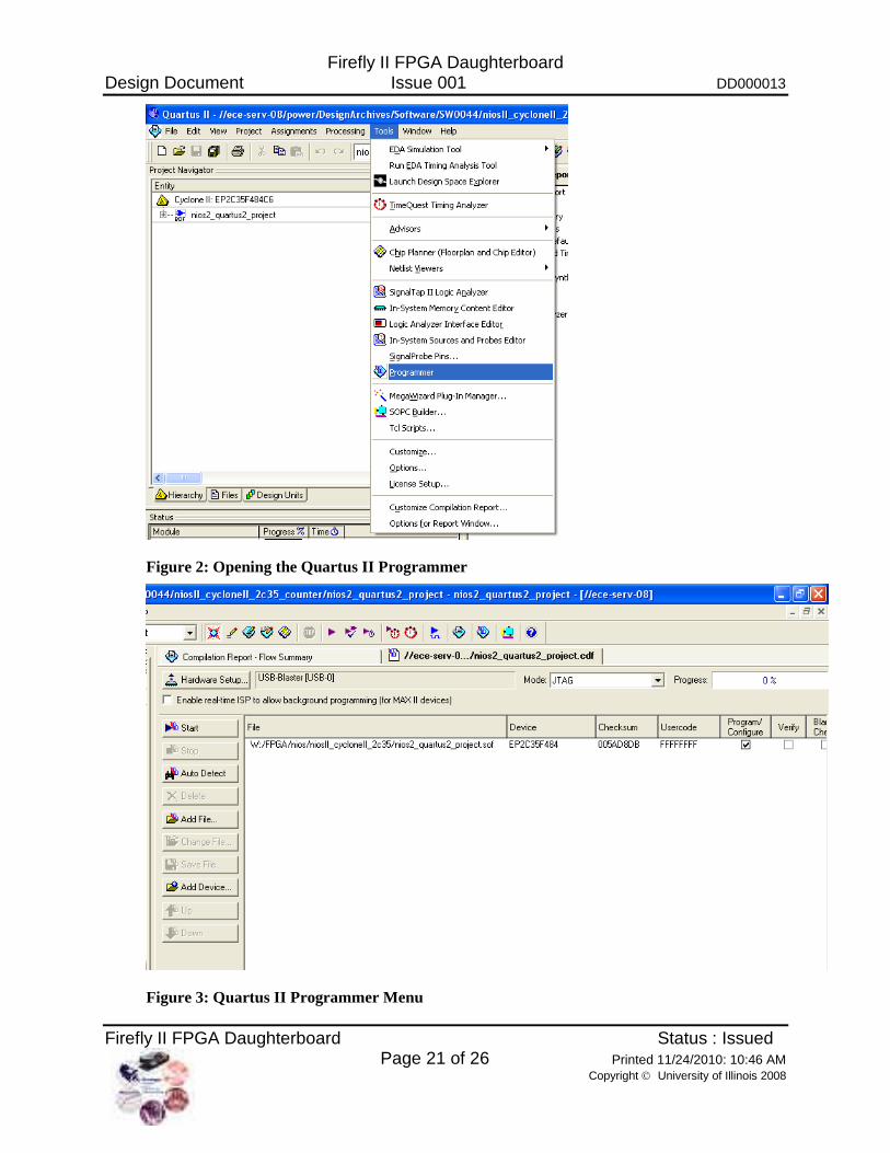
Firefly II FPGA Daughterboard Design Document Issue 001 DD000013
Firefly II FPGA Daughterboard Status : Issued Page 21 of 26 Printed 11/24/2010: 10:46 AM
Copyright University of Illinois 2008
Figure 2: Opening the Quartus II Programmer
Figure 3: Quartus II Programmer Menu
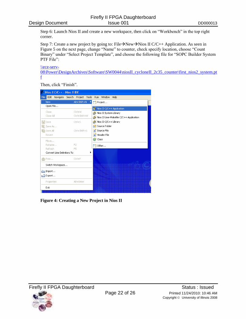
Firefly II FPGA Daughterboard Design Document Issue 001 DD000013
Firefly II FPGA Daughterboard Status : Issued Page 22 of 26 Printed 11/24/2010: 10:46 AM
Copyright University of Illinois 2008
Step 6: Launch Nios II and create a new workspace, then click on “Workbench” in the top right
corner.
Step 7: Create a new project by going to: FileNewNios II C/C++ Application. As seen in
Figure 5 on the next page, change “Name” to counter, check specify location, choose “Count
Binary” under “Select Project Template”, and choose the following file for “SOPC Builder System
PTF File”:
\\ece-serv-
08\Power\DesignArchives\Software\SW0044\niosII_cycloneII_2c35_counter\first_nios2_system.pt
f
Then, click “Finish”.
Figure 4: Creating a New Project in Nios II

Firefly II FPGA Daughterboard Design Document Issue 001 DD000013
Firefly II FPGA Daughterboard Status : Issued Page 23 of 26 Printed 11/24/2010: 10:46 AM
Copyright University of Illinois 2008
Figure 5: Nios II New Project Settings
Step 9: Right-click counter, go to “System Library Properties”, and turn off everything except for
“Program never exits” and “Small C library”. This step reduces compilation time.

Firefly II FPGA Daughterboard Design Document Issue 001 DD000013
Firefly II FPGA Daughterboard Status : Issued Page 24 of 26 Printed 11/24/2010: 10:46 AM
Copyright University of Illinois 2008
Figure 6: System Library Properties Menu
Step 10: Replace the code found in count_binary.c and count_binary.h, with the code found in:
\\ece-serv-
08\Power\DesignArchives\Software\SW0044\nios\niosII_cycloneII_2c35_counter\software\counte
r\counter.c
\\ece-serv-
08\Power\DesignArchives\Software\SW0044\nios\niosII_cycloneII_2c35_counter\software\counte
r\counter.h
Step 11: Rename count_binary.c and count_binary.h to counter.c and counter.h.
Figure 7: Renaming Project Files

Firefly II FPGA Daughterboard Design Document Issue 001 DD000013
Firefly II FPGA Daughterboard Status : Issued Page 25 of 26 Printed 11/24/2010: 10:46 AM
Copyright University of Illinois 2008
Step 12: Save the files, then right-click on the counter project, go to “Run As” then select “Nios II
Hardware”.
Note: Initial compilation may take a few minutes.
Figure 8: Running Nios II Code on the FPGA
Step 13: After the program loads, the blue light on the USB-Blaster should light up indicating the
JTAG link has been established. Figure 9 below and Figure 10 on the next page show the console
and FPGA outputs that should occur, respectively. Pressing the red button in Figure 10 will end the
JTAG link, allowing the code to be edited then rerun on the FPGA.
Figure 9: Nios II JTAG Console Output
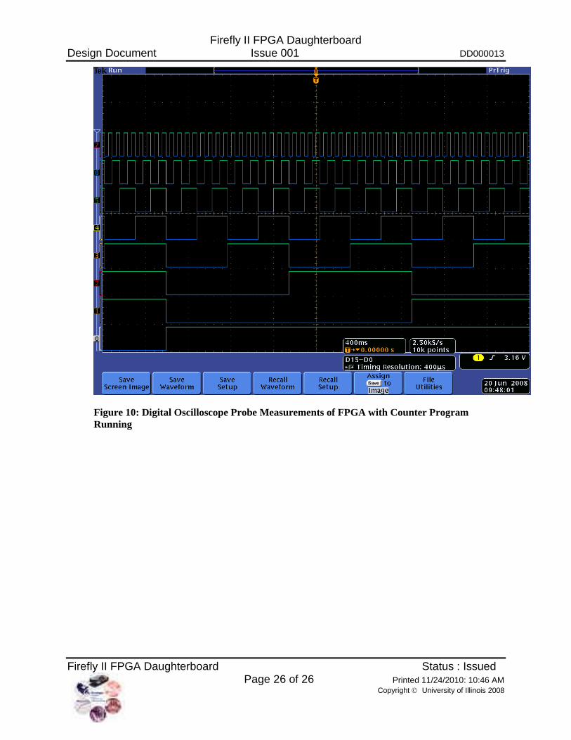
Firefly II FPGA Daughterboard Design Document Issue 001 DD000013
Firefly II FPGA Daughterboard Status : Issued Page 26 of 26 Printed 11/24/2010: 10:46 AM
Copyright University of Illinois 2008
Figure 10: Digital Oscilloscope Probe Measurements of FPGA with Counter Program
Running
Grainger Center for Electric Machinery and Electromechanics Department of Electrical and Computer Engineering
University of Illinois at Urbana-Champaign 1406 W. Green St.
Urbana, IL 61801
The information contained in this Document and the Appendices may not be copied, reproduced, distributed or stored in a retrieval system without the prior express written permission of the author.
Copyright Board of Trustees of the University of Illinois 2005. All Rights Reserved
Design Document
Modular Inverter Power Stage
Reference: DD00010
Issue: 001
Status: Issued
Author: Marco Amrhein / Brett Nee
Updated: Ali M. Bazzi / Kieran Levin
Principal Investigator: J. Kimball
Created: July 25, 2005
Updated: Nov. 23, 2010
\\cts-file-02\power\DesignArchives\Documents\Design Documents\ DD00010-001 Modular Inverter Power Stage.doc
Abstract:
This document describes the functionality and design details of the power stage module from the
Modular Inverter Project. The module itself consists of the power electronics components, gate
drives, signal measurements and conditioning, fault logic and dead-time implementation for the
gate signals. The power stage module was designed for a variety of voltage and power ranges and
can be used with IGBTs and MOSFETs.

Modular Inverter Power Stage Design Document Issue 001 DD00010
Modular Inverter Power Stage Status : Issued Page 2 of 36 Printed 11/24/2010: 10:44 AM
Copyright University of Illinois 2005
Document Revision History
Issue Date Comments
000 04/24/2006 Initial Release 001 11/23/2010 Testing procedure updated
Contents
1. Introduction ......................................................................................................... 4
1.1 Scope ..................................................................................................................................... 4
1.2 Definitions............................................................................................................................... 4
1.3 References ............................................................................................................................. 4
2. Electrical Design ................................................................................................. 5
2.1 Overview ................................................................................................................................ 5
2.2 Power Electronics Devices and Power Connections ............................................................. 5
2.2.1 MOSFET-Version .............................................................................................................. 6
2.2.2 IGBT-Version .................................................................................................................... 7
2.3 PCB Power Requirements ..................................................................................................... 7
2.3.1 Grounding ......................................................................................................................... 7
2.3.2 Isolated Power Supplies for Gate Drives .......................................................................... 8
2.4 Gate Drives ............................................................................................................................ 8
2.4.1 DC-Bus Connection for Low-Side Gate Drives ................................................................. 9
2.5 Control Board Interface .......................................................................................................... 9
2.6 Current Sensors and Current Measurement ........................................................................ 10
2.6.1 Dc Bus Current Calculation ............................................................................................. 11
2.7 Phase and dc Bus Voltage Measurement ............................................................................ 11
2.7.1 Isolated Voltage Amplifier ............................................................................................... 11
2.7.2 Offset Adjustment and Signal Amplification .................................................................... 12
2.7.3 How to Calibrate the Voltage Measurements ................................................................. 12
2.8 Dc Bus-Overvoltage and Phase-Overcurrent Detection ...................................................... 13
2.9 Logic ..................................................................................................................................... 13
2.9.1 CPLD Programming ........................................................................................................ 13
2.9.2 Gate Signal Selection and Lockout ................................................................................. 16
2.9.3 Dead Time Implementation ............................................................................................. 16
2.9.4 Fault-Logic ...................................................................................................................... 16
2.10 Temperature Measurement.................................................................................................. 17
3. Mechanical Design ........................................................................................... 18
3.1 Physical Board Outline ......................................................................................................... 18
Modular Inverter Power Stage Design Document Issue 001 DD00010
Modular Inverter Power Stage Status : Issued Page 3 of 36 Printed 11/24/2010: 10:44 AM
Copyright University of Illinois 2005
3.2 Front Panel ........................................................................................................................... 19
4. Known Issues ................................................................................................... 20
4.1 Dc-Bus and Phase Voltage Measurement ........................................................................... 20
4.2 Low-Current Transducers .................................................................................................... 20
5. Test Procedure ................................................................................................. 21
5.1 Original Test Procedure ....................................................................................................... 21
5.2 Revised Test Procedure ....................................................................................................... 25
6. Appendix ........................................................................................................... 30
6.1 Bill of Materials ..................................................................................................................... 30

Modular Inverter Power Stage Design Document Issue 001 DD00010
Modular Inverter Power Stage Status : Issued Page 4 of 36 Printed 11/24/2010: 10:44 AM
Copyright University of Illinois 2005
1. Introduction
The power stage module is the output stage / inverter of the modular inverter. It applies the gate
signals generated by the control stage to power electronics switches, handles hardware
implemented faults and measures and conditions analog signals necessary for the control of the
drive. It communicates with the control board, and takes the dc power from either the front end
module or from an external dc power supply.
1.1 Scope
The power stage module of the modular inverter consists of four phase legs that can be controlled
independently and configured with either IGBTs or MOSFETs. To control the gate drives
corresponding to each switch, a CPLD is programmed with dead-time logic for each phase leg and
with a fault-logic to stop the switching action in case of a fault. Various analog signals necessary
for motor control and monitoring the drive operation are measured on the board, conditioned and
fed back to the control stage. The power stage communicates exclusively with the control stage
with analog and digital signals.
This document describes the power stage module and will give detailed information about each of
the sub-modules on the board, the communication with the control board and the input power
requirements. Also, the various configurations with IGBTs and MOSFETs as well as the various
voltage and current ranges possible are discussed.
1.2 Definitions
1.3 References
Schematic: SK0031 rev 4
Layout: PB0031 rev D
Mechanical design: PJ0019, DR0016 (PCB mechanical outline)
CPLD program: SW0012, Inv_Logic_v3

Modular Inverter Power Stage Design Document Issue 001 DD00010
Modular Inverter Power Stage Status : Issued Page 5 of 36 Printed 11/24/2010: 10:44 AM
Copyright University of Illinois 2005
2. Electrical Design
2.1 Overview
The control signals (logic level) for the four phase-legs of the inverter arrive from the control board
via a defined interface. A CPLD conditions those signals, applies a lockout mechanism and dead
time, and sends the gate signals to the appropriate gate drives. The gate drives create gates signal
from the logic-level signals that can drive the individual MOSFETs or the IGBTs.
The power stage can be configured in three different ways to accommodate the needs of the users.
The configurations are given in Table 1. The low-voltage high current (100V, 40ARMS)
configuration and the high-voltage low-current (400V, 10ARMS) configuration use MOSFETs, and
the high-voltage high-current (400V, 40ARMS) configuration uses IGBTs.
The phase outputs of the power electronics devices are routed through current sensors in order to
measure each phase current. In addition, all phase voltages are measured, as well as the bus
voltage. The bus current is calculated as the sum of the four phase currents. Two temperature
measurement circuits are included on the board, but are not used for any specific tasks. All those
signals are fed back to the control board via a defined interface. Minimum filtering is applied to
those signals.
Overcurrent and overvoltage detection circuits are used in order to detect overcurrents in the four
phases or an overvoltage in the dc bus voltage. Together with the fault signals created by the gate
drive chips in case of a gate drive fault, these faults are fed back to CPLD, which in-turn disables
all gate drives and communicates a fault to the control board. This state can only be reset by a
RESET command from the control board, or the built-in reset-button from the power stage.
A general comment about the operation amplifiers used in the power stage module is necessary at
this point. Since the voltage and current measurements are measuring the actual waveform of the
signal and not an average or rms value, fast devices that can adequately represent the switching
waveforms need to be used. The operational amplifiers chosen are the TLE2082 (dual opamp) and
the TLE2084 (quad opamp), which have a three times higher slew rate and twice the bandwidth of
a conventional TL082.
2.2 Power Electronics Devices and Power Connections
As was mentioned previously, the board can be configured to work with IGBTs or MOSFETs. The
setup of the two different possibilities is described in this Section. The main difference is that the
IGBTs cannot be mounted on the PCB, meaning that the power path of the dc bus is removed from
the board (the IGBTs are connected with bus bars). However, the MOSFETs are mounted on the
PCB, meaning that the main power path of the dc bus is actually on the board.
Table 1. Inverter Power Stage Configurations
Max. dc bus voltage Rated RMS current PE Devices PE Component
100 V 40 A MOSFET IRFPS3815
400 V 10 A MOSFET IRFPS40N50L
400 V 40 A IGBT BSM100GB60DLC

Modular Inverter Power Stage Design Document Issue 001 DD00010
Modular Inverter Power Stage Status : Issued Page 6 of 36 Printed 11/24/2010: 10:44 AM
Copyright University of Illinois 2005
The two electrolytic dc bus capacitors C161 and C162 (1200 F, 450 Vdc, Part # ECE-
T2WP122FA from Panasonic-ECG) are mounted on the board for both IGBTs and MOSFETs due
to simplicity. However, in order to avoid dc bus loops on the PCB when IGBTs are used, the
positive dc bus copper plane (TOP plane at the top of the layout) was split. This way, the two
electrolytic capacitors can be connected to the dc bus without creating any dc bus loop on the PCB.
All wires to and from the PCB board are intended to be connected through soldering holes, which
are large enough to support 14 gauge wires for the power connections, and 20 gauge wires for the
gate drive connections, where applicable. For both configurations, the phase output wires need to
be connected to J28, J29, and J30 for Phase A, to J34, J35, and J36 for Phase B, to J40, J41, and
J42 for Phase C, and to J46, J47, and J48 for Phase D. Three wires in parallel support at least a
current of about 60 ARMS continuously, which is large enough for the capabilities of the inverter.
2.2.1 MOSFET-Version
Any MOSFETs can be used that fit a TO-274AA (Super-247) package. The MOSFETs are
clamped to the heatsinks, so no mounting holes need to be provided. The MOSFETs that are
intended to be used are IRFPS3815 for a low-voltage high-current configuration (100 Vdc, 40 ARMS)
of the inverter, and IRFPS40N50L for a high-voltage low-current configuration (400 Vdc, 10 ARMS).
In the MOSFET configuration, the positive dc bus input can be connected either to J13, J14, and
J15 (next to C162) or to J16, J17, and J18 (next to C161). Do not connect to both sets at the same
time to avoid loops. Analog, the negative dc bus input can be connected either to J19, J20, and J21,
or to J122, J23, and J24. In addition, the split in the positive dc bus needs to be short-circuited by
using 14-gauge wire bridges from J62 to J63, J64 to J65, J66 to J67, and J68 to J69.
In the gate drive section of each MOSFET, jumper wires are necessary in order to connect the
MOSFET correctly to the gate drive. For example, for the Phase A high-side MOSFET (Q1),
jumper connections need to be made on component J3 from each bottom hole to the corresponding
hole on the top, using 20 gauge wire, as shown in Figure 1a. The same connections need to be
made at the components J4 through J10.
Additional capacitors (C157, C158, C159, and C160) need to be mounted close to each pair of
MOSFETs in order to improve the switching performance. The capacitors are film capacitors,
0.56 F, rated for 630 Vdc (Cornell Dubilier, Part # DME6P56K).
AWG 20 wire
C/D E/S Gate
AWG 20 wire
to IGBT
collector to IGBT
emitter
to IGBT
gate
C/D E/S Gate
a) MOSFET b) IGBT
Figure 1. Gate drive jumper connection diagram.

Modular Inverter Power Stage Design Document Issue 001 DD00010
Modular Inverter Power Stage Status : Issued Page 7 of 36 Printed 11/24/2010: 10:44 AM
Copyright University of Illinois 2005
2.2.2 IGBT-Version
The IGBTs used are Eupec’s BSM100GB60DLC, a 600 Vdc single-phase IGBT bridge rated for
100 ARMS. The four modules required for the inverter are mounted to the heatsinks. The dc bus is
connected to the IGBTs via bus bars, meaning that the main power does not need to be connected
to the power stage PCB. However, the two electrolytic capacitors need to be wired to the dc bus.
For C161, the positive dc bus needs to be wired to J16, J17 or J18 (one single 14 gauge wire is
sufficient), and the negative dc bus to J22, J23, or J24. Similar, for C162, the positive dc bus needs
to be connected to J13, J14, or J15, and the negative dc bus to J19, J20, or J21.
An additional capacitor (2 F 1000 Vdc, Cornell Dubilier, Part # SCD205K102A3Z25) is mounted
directly on each IGBT module. Therefore, the components C157 to C160 are left empty. Also, the
positive dc bus on the left and on the right side of the board is not connected together to avoid
loops.
The gate drives are connected to the IGBTs using 20 gauge wires as shown in Figure 1b. The
IGBT modules have separate pins for gate and emitter connections. The collector wire needs to be
connected to the positive dc bus for the high-side IGBTs in each phase-leg, and to the individual
phase output for the low-side IGBTs. The connections should be as short as possible to minimize
the inductance. The three holes on the top of each jumper shall be left unconnected.
The phase output of each IGBT module needs to be wired back to the PCB board for current and
voltage measurements using three 14 gauge wires. Wire connections above the current sensor are
available in for each phase (Phase A: J25, J26, J27, Phase B: J31, J32, J33, Phase C: J37, J38, J39,
Phase D: J43, J44, J45).
2.3 PCB Power Requirements
The various circuits on the PCB require different supply voltages for analog and logic components.
The analog circuits and the isolated power supplies for the gate drives require ±15 Vdc and roughly
0.7 A, whereas the logic circuits require +5 Vdc and about 0.8 A. The connector J49 (4-pin
MTA156) is used for those supply voltages plus GND. Two footprints for NTC resistors (CL-160,
RT1 and RT2) are provided in case the inrush current needs to be limited on the ±15 Vdc to avoid
power supply faults. Normally, RT1 and RT2 can be short-circuited.
Support capacitors footprints are provided throughout the board for all voltage levels. At the
connection to the power supplies, 220 F electrolytic capacitors and 0.1 F film capacitors should
be used (C164 to C169). Additional 10 F electrolytic capacitors and 0.1 F film capacitors
footprints are provided along the main power traces and can be stuffed if needed.
Two power control LEDs are mounted on the front panel of the power stage module, and indicate if
both +15 V and –15 V power is available. These LEDs are connected via a 3-pin MTA100
connector (J61).
2.3.1 Grounding
Two different grounds are provided on the board, analog ground (COM_A) and logic or digital
ground (COM_D). They are separated in order to keep the logic signals, which include all the gate
signals plus fault indication, as noise-free as possible. These two grounds are connected to the
power supply via resistors R121 for COM_A and R122 for COM_D. R121 and R122 should be
short-circuited (COM_A = COM_D).

Modular Inverter Power Stage Design Document Issue 001 DD00010
Modular Inverter Power Stage Status : Issued Page 8 of 36 Printed 11/24/2010: 10:44 AM
Copyright University of Illinois 2005
Earth ground can be connected to the board if desired through wire connector J60 (14 gauge wire),
which will connect the power supply ground to earth ground. Footprints are provided for a resistor
and a capacitor between power supply ground and earth ground.
2.3.2 Isolated Power Supplies for Gate Drives
The isolated power supplies required for the gate drives are on separate PCBs (PB0032). They
draw the power from the ±15 V supply, and are connected via 3-pin MTA100 connectors. Each
high-side gate drive requires one isolated power supply, and all low-side gate drives require another
one. The connector configuration (J50 for Phase A high-side power supply, J52 for Phase B, J54
for Phase C, J56 for Phase D, and J58 for low-side power supply) is as follows: Pin 1 is +15 V,
Pin 2 COM_D. and Pin 3 –15 V.
The isolated output voltages of each power supply are +15 V, +5 V, GND, and roughly–7 V. For
the four high-side gate drives, +5 V is not required. Thus, the power supplies are connected via 3-
pin MTA100 connectors (J51 for Phase A, J53 for Phase B, J55 for Phase C, and J57 for Phase D)
with the following pin configuration: Pin 1 is +15 V, Pin 2 is GND, and Pin 3 is –7 V. The low-
side power supply needs to deliver the +5 V output in order to power the isolated voltage
amplifiers, which are, similar as the low-side gate drives, referenced to the negative dc bus. A 4-
pin MTA100 connector is used (J59), with Pin 4 connected to +5 V, and the other pins connected
like the other power supplies.
2.4 Gate Drives
Each power electronic device has its own gate drive, which basically consists of a single chip with
some external components. The gate drive chip used is an HCPL-316J, a 16 pins surface-mount
part. The chip takes logic-level switching signals, and outputs gate signals for the power
electronics devices.
The circuitry for each gate drive is taken from the HCPL-316J datasheet. The gate signals are
applied to the positive gate signal input pin, and the gate drive enable signal (~GD_ENABLE) is
applied to the negative gate signal input pin. The gate drive turns on only when the positive pin is
logic high, and the negative pin logic low. Thus, the negative input pin is used to disable the gate
drives and the power electronic devices in case of a fault.
On the output side of the gate drive, all resistors need to be ½ W, 1% tolerance (except where
indicated) due to the large power dissipation. The capacitors need to be rated for at least 25 V.
Few components need to be selected according to the configuration of the power stage module.
Values for the gate resistance Rg and the resistance Rc are given in Table 2. The capacitance Cg is
added in the schematic to provide the flexibility of increasing the gate capacitance. In general, this
component does not need to be stuffed, and there are no recommended values available.
For the low-voltage inverter configuration (100 V), the DESAT diode used is a 1N4148 (5 in
series). For the high-voltage inverter configuration (400 V), the DESAT diode is one MUR160,
and the other four positions need to be short-circuited. The DESAT diode specifications are given
in Table 2.
The connection of each power electronics device to the gate drive needs to be done via the 6-
position jumpers is described in Sections 2.2.1 and 2.2.2 and in Figure 1.

Modular Inverter Power Stage Design Document Issue 001 DD00010
Modular Inverter Power Stage Status : Issued Page 9 of 36 Printed 11/24/2010: 10:44 AM
Copyright University of Illinois 2005
2.4.1 DC-Bus Connection for Low-Side Gate Drives
The layout has one issue with the ground connection of the four low-side gate drives. They are
powered by the same power supply, which is referenced to the negative dc bus. Short-circuiting
jumper J70 (close to dc bus capacitor C162) connects the ground of the low-side gate drives to the
negative dc-bus at one connection.
2.5 Control Board Interface
Two interface connectors for communication with the control board were specified at the beginning
of the project, one for analog and one logic signals. The physical connection is established with
non-shielded flat ribbon cable through vertical LATCON connectors. The specification of the 26-
pin connector for the analog signals is given in Table 3, and of the 34-pin connector for the logic
signals in Table 4.
The analog signals are transmitted through buffer circuits / voltage followers (U16, U17, U18).
The logic signals are transmitted as RS-422 differential pairs, using a DS26LS31 transmitter (U37)
and DS26LS32 receivers (U39, U40, U41). For the receivers, the transmission lines are terminated
with 143 resistors. Critical signals such as ENABLE and uC_RESET are tied to COM_D,
Table 2. Gate Drive Configurations
Inverter Configuration PE devices Rg Rc DESAT diode
100 V / 40 ARMS MOSFET 15 (1/2 W) 0 1N4148 (4 or 5 in series)
400 V / 10 ARMS MOSFET 47.5 (1/4 W) 0
MUR160 (only 1, the other
pos. short-circuited))
400 V / 40 ARMS IGBT 47.5 (1/4 W) 0
MUR160 (only 1, the other
pos. short-circuited)
Table 3. Analog Connector to Control Board.
Pin Signal Description Pin Signal Description
1 COM_A Analog ground 14 KELVIN2 Analog ground
2 NC Not connected 15 RESERVED
3 NC Not connected 16 RESERVED
4 COM_A Analog ground 17 RESERVED
5 IA Phase A current 18 RESERVED
6 IB Phase B current 19 KELVIN3 Analog ground
7 IC Phase C current 20 COM_A
8 ID Phase D current 21 COM_A
9 KELVIN1 Analog ground 22 VA Phase A voltage
10 VBUS Dc bus voltage 23 VB Phase B voltage
11 T1 Temperature 1 24 VC Phase C voltage
12 T2 Temperature 2 25 VD Phase D voltage
13 IBUS Dc bus current 26 KELVIN4 Analog ground

Modular Inverter Power Stage Design Document Issue 001 DD00010
Modular Inverter Power Stage Status : Issued Page 10 of 36 Printed 11/24/2010: 10:44 AM
Copyright University of Illinois 2005
respectively their complementary signals to +5 V, through 1 k resistors in order to guarantee that
the inverter is disabled when no communication is present between the power stage and the control
board. For those signals (and the reserve signals), the terminating resistors are 200 , which
together with the 1 k resistors result in a terminating resistance of 143 .
2.6 Current Sensors and Current Measurement
Closed-loop current transducers using the Hall effect from LEM are used. For the two different
current ranges featured in the power stage, two current sensors were chosen that fit in the same
footprint, see Table 5. The transducers output a current that is proportional to the actual current,
and is converted into a voltage via a burden resistance. The burden resistor can be adjusted for
each phase to four different values using the switches SW1, SW2, SW3, and SW4, and the DIP-
resistors RN1, RN2, RN3, and RN4. Activating the switches adds more resistors in parallel to the
burden, thus increasing the measured current at a certain output voltage level. The output voltage
is calculated using the formula
1b
I m
RV I
x scale , (1)
Table 4. Logic Connector to Control Board
Pin Signal Description Pin Signal Description
1 NC Not connected 18 ~D1
2 COM_D Logic ground 19 D2 Gate signal D2
3 NC Not connected 20 ~D2
4 COM_D Logic ground 21 ENABLE Switching enable
from control 5 A1 Gate signal A1
22 ~ENABLE
6 ~A1 23 FAULT Inverter fault to
control 7 A2 Gate signal A2
24 ~FAULT
8 ~A2 25 uC_RESET Fault reset from
control 9 B1 Gate signal B1
26 ~uC_RESET
10 ~B1 27 RESERVED
11 B2 Gate signal B2
28 RESERVED
12 ~B2 29 RESERVED
13 C1 Gate signal C1
30 RESERVED
14 ~C1 31 RESERVED
15 C2 Gate signal C2
32 RESERVED
16 ~C2 33 RESERVED
17 D1 Gate signal D1 34 RESERVED
Table 5. Current Transducer Choices
Inverter max. phase current Current transducer Max. current rating Current scaling
40 ARMS LAH 100-P 100 ARMS 1:2000
10 ARMS LAH 25-NP 25 ARMS 1:1000

Modular Inverter Power Stage Design Document Issue 001 DD00010
Modular Inverter Power Stage Status : Issued Page 11 of 36 Printed 11/24/2010: 10:44 AM
Copyright University of Illinois 2005
where Rb is the burden resistance, x the number of burden resistors in parallel, and scale the scaling
factor of the current transducer. Given a 1.8 k burden resistance and an output voltage VI of 4.5
V at rated RMS current of the inverter, the possible current ranges for both transducer choices are
given in Table 6. Other values for the burden resistance can be used, but the gain needs to be
adjusted in the filter stage such that the output voltage is 4.5 V at the rated RMS current for proper
functioning of the overcurrent detection circuit.
2.6.1 Dc Bus Current Calculation
The bus current is defined as the current flowing from the positive dc bus to the negative dc bus
through the power electronics devices. Assuming that they are ideal, the bus current is equal to the
sum of all phase currents through the high-side devices. Since an inverting adder circuit is used,
the bus current is calculated as the negative sum of all phase currents signals through the low-side
devices, i.e.
bus high phase low phaseI D I D I . (2)
A DG212CJ (quad SPST CMOS analog switch) is used to feed the corresponding current signal to
the adder circuit when one of the low-side switching devices is on. A small first-order filter with a
cut-off frequency of 1 MHz is used to band limit the bus current signal.
2.7 Phase and dc Bus Voltage Measurement
Each of the four phases as well as the dc bus voltage is measured with respect to the negative dc
bus. The principle of the measurement is very simple. An isolated voltage amplifier measures
translates the actual voltage into a low-level signal. This signal is then scalded and offset adjusted
such that the voltage signal is within a voltage range of ±10 Vdc. The actual calibration is that 8 V
corresponds to nominal dc bus voltage of the inverter (100 V or 400 V).
2.7.1 Isolated Voltage Amplifier
The isolated voltage amplifier used on this board is an HCPL-7800A with an integrated optical
isolation barrier. It requires two +5 Vdc voltages supplies, one referenced to the negative dc bus,
and one referenced to common ground. The dc bus referenced voltage is taken from the isolated
power supply that powers all low-side gate drives. The logic supply voltage with its logic ground
(COM_D) is used for common ground referenced voltage supply. This works although the
measured signal is an analog signal and is referenced to analog ground (COM_A), because the
isolated voltage amplifier chip has a differential input and output.
Table 6. Possible Current Ranges with 1.8 k Burden Resistor and 4.5 V Output
Voltage at RMS Current.
Switch positions
closed
# of parallel
resistors x
Total burden
resistance
RMS current for
LAH 100-P
RMS current for
LAH 25-NP
None 1 1.8 k 5 ARMS 2.5 ARMS
1 2 900 10 ARMS 5 ARMS
1 and 2 4 450 20 ARMS 10 ARMS
All 8 225 40 ARMS 20 ARMS

Modular Inverter Power Stage Design Document Issue 001 DD00010
Modular Inverter Power Stage Status : Issued Page 12 of 36 Printed 11/24/2010: 10:44 AM
Copyright University of Illinois 2005
For accurate operation of the isolated voltage amplifier, the differential input voltage should be less
than 200 mV. This is achieved by using up to four ¼ W resistors in series with a 1 k precision
pot. In the dc bus measurement schematic, these resistors are R126, R127, R130 and R133, and the
precision pot is R134. The values for the four resistors (RV in the schematic) are chosen according
to Table 7 for the different voltage ratings.
2.7.2 Offset Adjustment and Signal Amplification
The isolated voltage amplifier has a gain of roughly eight. In order to get an 8 V signal from the
rated dc bus voltage, an additional gain stage is necessary. The total gain required from the
differential input of the isolated voltage amplifier to the voltage signal is at least
_
840
0.2
outmin
diff max
V Vg
V V . (3)
The resistor combination in the amplifier stage yields a gain of 6.85. Combined with the isolated
voltage amplifier gain, the required differential input voltage for an 8 V signal is
8
1468 6.85
outdiff
V VV mV
g
, (4)
which can be achieved by adjusting the 1 k precision pot. The gain stage is has a band limit of
about 300 kHz, enforced through a capacitor in the additional gain stage.
One phenomenon observed with the isolated voltage amplifier is that it tends to have an offset
voltage at the differential outputs of varying magnitude up to about 300 mV. In order to correct for
that, an offset compensation was added to the circuit. Using 10 V zener diodes (1N4740), an offset
voltage determined by a 1 k precision pot is subtracted from the differential output signal of the
isolated voltage amplifier.
2.7.3 How to Calibrate the Voltage Measurements
Disconnect the phase connections and the dc bus connections from the board. The rated dc voltage
needs to be applied at the dc bus and at each of the phase terminals in order to calibrate each of the
voltage measurements. The analog and logic circuits need to be powered with the power supplies
used in the actual inverter to avoid incorrect voltage measurements once the power stage is
mounted in the inverter box.
First, the dc bus terminals (respectively the phase terminals to negative dc bus) need to be shorted.
With the 1 k precision pot, the voltage measurement signal needs to be adjusted to 0 V. Then, the
short is removed, and rated dc voltage is applied to the dc bus or phase terminal, respectively. With
the 1 k precision pot, the voltage signal can be adjusted to 8 V. This will likely introduce a small
offset voltage in the voltage signal when the terminal voltage is zero (important for the phase
voltage measurements). This can be corrected for by repeating the calibrating process once or
Table 7. Resistance values in voltage measurements for various voltage ranges.
Inverter dc bus voltage rating Resistor values RV
100 Vdc 4 times 124 k
400 Vdc 4 times 499 k

Modular Inverter Power Stage Design Document Issue 001 DD00010
Modular Inverter Power Stage Status : Issued Page 13 of 36 Printed 11/24/2010: 10:44 AM
Copyright University of Illinois 2005
twice until the desired accuracy is obtained (measurement within a few milivolts of the desired
value are possible).
The calibration process is described in more detail in the test procedure in Section 5.
2.8 Dc Bus-Overvoltage and Phase-Overcurrent Detection
The dc bus overvoltage protection should be activated when the bus voltage rises 17% above its
rated value. With the 8 V signal at rated voltage, this results in a trip level of 9.3 V. An LM311
comparator (U5) is used to compare the trip level to the measured dc bus voltage signal. The trip
level is generated using a 12V zener diode (1N4742) and with a resistive voltage divider. The
resistor R9 provides positive feedback and stabilizes the comparator operation by introducing a
hysteresis band of 50 mV.
The LM311 was chosen because its open-collector output transistor can be referenced to a separate
emitter voltage level at pin 1 (ordinary comparators are reference to the negative voltage supply).
Since all fault signals are logic-level signals, COM_D is connected to pin 1, and the pull-up resistor
R11 is connected to +5 V.
The overcurrent detection was specified to trip at 216% of the rated rms current in each phase leg.
With the corresponding rms current signal of 4.5 V, the trip level for an overcurrent fault is 9.71 V.
Since the current is an ac signal, both positive and negative peaks need to be checked for an
overcurrent in order to achieve an almost instant shutdown of operation. As in the overvoltage
detection, the trip voltage is generated with a 12 V zener diode and a resistive voltage divider.
LM311 comparators are used with wired-or outputs. The logic-level fault signal is generated the
same way as in the overvoltage detection. The 499 k resistor provides positive feedback and
stabilizes the comparator operation by introducing a hysteresis band of 40 mV.
2.9 Logic
The logic for the gate signal handling and the fault detection is implemented with 5 V parts. The
main part is a CPLD (U35, XC95108-PC84) that handles the gate-signal selection and lockout, the
dead time and the fault procedures as described in the following Sections. Few additional logic
components are needed for proper operation.
The CPLD runs on a 20 MHz clock (U38, ECS-100X-200 oscillator), which was chosen to
minimize the possible dead time between the high-side and low-side signal of one phase leg. With
the 20 MHz clock, the minimum dead time is 50 ns. The CPLD can be programmed through
connector J12.
2.9.1 CPLD Programming
1. Preparation
Before you start, please check that the following are available to you:
Xilinx ISE (8.1 or higher)
Jtag programmer supported by the ISE. In this tutorial we use a Xilinx platform cable
USB, model DLC9.
A modular inverter power-stage board ready.
A 5 V power supply.
Xilinx XC95108 CLPD
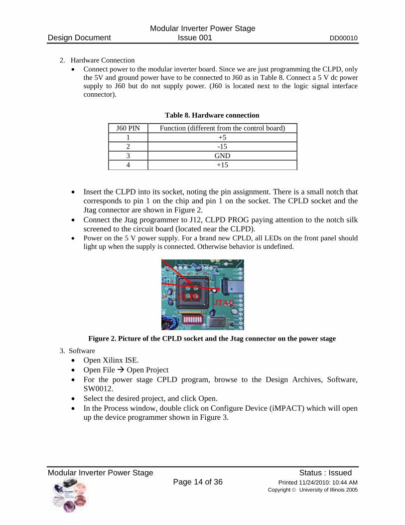
Modular Inverter Power Stage Design Document Issue 001 DD00010
Modular Inverter Power Stage Status : Issued Page 14 of 36 Printed 11/24/2010: 10:44 AM
Copyright University of Illinois 2005
2. Hardware Connection
Connect power to the modular inverter board. Since we are just programming the CLPD, only
the 5V and ground power have to be connected to J60 as in Table 8. Connect a 5 V dc power
supply to J60 but do not supply power. (J60 is located next to the logic signal interface
connector).
Table 8. Hardware connection
Insert the CLPD into its socket, noting the pin assignment. There is a small notch that
corresponds to pin 1 on the chip and pin 1 on the socket. The CPLD socket and the
Jtag connector are shown in Figure 2.
Connect the Jtag programmer to J12, CLPD PROG paying attention to the notch silk
screened to the circuit board (located near the CLPD). Power on the 5 V power supply. For a brand new CPLD, all LEDs on the front panel should
light up when the supply is connected. Otherwise behavior is undefined.
Figure 2. Picture of the CPLD socket and the Jtag connector on the power stage
3. Software
Open Xilinx ISE.
Open File Open Project
For the power stage CPLD program, browse to the Design Archives, Software,
SW0012.
Select the desired project, and click Open.
In the Process window, double click on Configure Device (iMPACT) which will open
up the device programmer shown in Figure 3.
J60 PIN Function (different from the control board)
1 +5
2 -15
3 GND
4 +15

Modular Inverter Power Stage Design Document Issue 001 DD00010
Modular Inverter Power Stage Status : Issued Page 15 of 36 Printed 11/24/2010: 10:44 AM
Copyright University of Illinois 2005
Figure 3. Process window
6. A window will open asking what type of boundary mode scan to perform. Select
"Automatically connect to cable and identify Boundary-Scan chain” and click finish.
7. iMPACT should connect to the device. If not, check your connections.
8. The software will now ask for a configuration file. Select logic.jed
9. Select the Chip in the boundary scan window by clicking on it as shown in Figure
4.
Figure 4. Boundary scan window
10. Click on Operations Program
11. Make sure that Program and Verify are selected.
12. Click OK.
13. Wait for the device to be programmed and verified. The programming should
take about a minute.
14. You have completed Programming the CLPD. All Error lights on the front panel
should now be off if programming succeeded.

Modular Inverter Power Stage Design Document Issue 001 DD00010
Modular Inverter Power Stage Status : Issued Page 16 of 36 Printed 11/24/2010: 10:44 AM
Copyright University of Illinois 2005
2.9.2 Gate Signal Selection and Lockout
The gate signals from the control board get to the CPLD via the quad receiver chips previously
mentioned. Two modes of operation can be chosen. The first mode assumes that only the high-
side gate signal of each phase leg is transmitted to the CPLD, and the low-side gate signals are
generated as the complement of the high-side signals. The second mode assumes that both high-
and low-side gate signals are available. This selection can be done externally with Jumper JP1. If
it is set to +5 V (logic high), then the first mode (only high-side gate signals) is active, and if it is
connected to COM_D (logic low), the second mode (all gate signals) is active. It is not possible to
select the mode of operation for each individual phase leg, but rather for the whole inverter.
To avoid that both gate drives in one phase leg receive a turn-on command, the two gate signals in
one phase leg are fed through a lockout logic. This logic simply prevents both gate signals being
logic high at the same time, and sets them to logic low.
For the detailed schematic, refer to SW0012, Inv_Logic_v3, Mode Selection.
2.9.3 Dead Time Implementation
Each phase leg has its own dead time logic. The dead time can be determined with the 8-bit switch
SW5, by adding one to the corresponding decimal value and multiplying it by 50 ns. The lowest
bit is on the right side of SW5, and the highest bit on its left side. Due to the implementation of the
logic, it is not possible to turn all bits on or off at the same time. The maximum dead time possible
is therefore
82 1 50 12.75d_maxt ns s , (5)
and the minimum dead time
2 50 100d_mint ns ns . (6)
The dead time logic enforces a certain amount of time where both gate signals of one phase leg are
logic low (switch off) in between switching processes. Basically, every time one of the gate signals
switches off, the dead time circuit prevents the other gate signal from turning on for a certain
amount of time.
Since the CPLD runs on a fixed clock, the gate signals need to be synchronized to this clock first.
After receiving the signals from the mode selection and lockout circuit, four D flip-flops detect
falling edges in either one of the two gate signals of one phase leg. Each falling edge triggers an 8-
bit counter to be loaded with the 8-bit dead time selected with SW5. The countdown process is
automatically started by the fact that the counter state is not zero anymore, and stops as soon as the
counter reaches zero.
The rising edge of a gate signal sets the output of a JK flip-flop to high, which is in turn used to
prevent the other gate signal from being on (even if it would be commanded). This flip-flop is reset
when the same gate signal turned off and the counter reached its zero state. After that, both gate
signals have the possibility of turning on again. Two JK flip-flops are used per phase leg, one for
each gate signal.
For the detailed schematic, refer to SW0012, Inv_Logic_v3, Dead Time Logic.
2.9.4 Fault-Logic

Modular Inverter Power Stage Design Document Issue 001 DD00010
Modular Inverter Power Stage Status : Issued Page 17 of 36 Printed 11/24/2010: 10:44 AM
Copyright University of Illinois 2005
Nine different faults are monitored on the power stage board: four overcurrents (each phase), one
overvoltage (dc voltage) and four gate drive faults (four pairs of gate drives that are wired-or
connected). Each of the faults trips the fault logic in the CPLD, which activates the fault signal
going to the control board (logic low). In addition, it disables all the gate drives by setting the
negative gate signal input of each gate drive to logic high (GD_VIN_NEG in CPLD program, or
GD_ENABLE in schematic). The faults are stored in the CPLD, and need to be reset either
manually with a pushbutton or with the uC-RESET signal from the control board. Three different
fault conditions are indicated with LEDs: overcurrent, overvoltage, and gate drive fault, in addition
to the information in which phase the fault occurred in case of an overcurrent or gate drive fault.
The LEDs are connected at J11.
The fault-reset logic uses the two different reset signals (uC-RESET and PWR-UP) to create a low
pulse on the GD-RESET signal (RESET-GD in schematic) for at least 50 s, which is long enough
to reset the gate drives if they are in fault state. On the rising edge of GD-RESET, the stored faults
in the CPLD are reset, and the gate drives are enabled again. The uC-RESET signal from the
control board needs to be a positive pulse of at least 100 ns. The PWR-UP signal is created by a
pushbutton connected through J11 and a voltage supervisor U36. The voltage supervisor also takes
care of the power-up of the board by setting the PWR-UP signal to low for about 1 s, which in turns
disables the gate drives and prevents switching.
The gate drives also need to be enabled by the control box with the signal ENABLE. A high state
will set the signal GD_VIN_NEG to a low-level if there is no fault present, which in turn enables
the gate drives to switch.
For the detailed schematic, refer to SW0012, Inv_Logic_v3, Fault Logic.
2.10 Temperature Measurement
Two temperature measurements are provided in order to monitor device temperatures or ambient
temperatures in the inverter box. The temperature signals are fed back to the control board, where
they could be monitored and the inverter can be disabled if the temperature is too high. The
sensors are LM35s in a TO-92 package (U1 and U3), which have a 10 mV/°C output signal. The
signals are amplified such that 20°C correspond to 1 V.

Modular Inverter Power Stage Design Document Issue 001 DD00010
Modular Inverter Power Stage Status : Issued Page 18 of 36 Printed 11/24/2010: 10:44 AM
Copyright University of Illinois 2005
3. Mechanical Design
3.1 Physical Board Outline
The physical outline of the mounting holes for the mounting of the power supplies and the PCB
itself are given in Figure 5 below.
D C B A
43
21
D C B A
43
21
TIT
LE M
oun
tin
g h
ole
s,
Pow
er
Sta
ge P
CB
DR
AW
N B
Y
M.
AM
RH
EIN
SC
AL
E
1:
2.5
DW
G N
O
DR
001
5
RE
V
AC
HE
CK
ED
BY N
ON
E
17
"
11"
0.5" 0.875"
5.125"
10.2
1.6
25
"
6.1
25"
3.6
75
"4
.95"
2.3
75"
6.3
75
"4.5
"
3.7
75"
4.6
"
PS
AP
S C
PS
D
2"3.375"
1.6
25"
3.5
"3
.25"
3.2
5"
3.5
"1.8
75
"
2.5
"1
"2.5
"2
.5"
2.5
"1
"2.5
"0
.625"
PS
BP
S L
ow
9.625"
Moun
tin
g H
ole
sP
CB
Shelf
Slo
ts c
ove
red b
y b
rackets
0.3
75"
0.7
5"
0.7
5"
Figure 5. Mechanical PCB outline with mounting shelf.

Modular Inverter Power Stage Design Document Issue 001 DD00010
Modular Inverter Power Stage Status : Issued Page 19 of 36 Printed 11/24/2010: 10:44 AM
Copyright University of Illinois 2005
3.2 Front Panel
The front panel layout of the inverter power stage is shown in Figure 6. The fault signals are: OV
– Overvoltage on dc bus; OC – Overcurrent in Phase A, B, C, or D; GD – Gate drive fault in Phase
A, B, C, or D.
NOTES
1. Dashed items are reference only
2.5
5
3.5
50
.00
0.00
3.0
5
1.79 7.00 8.00
8.50
9.00
9.50
10.00
10.50
11.00 12.00
11X Ø 0.25
19.00
5.2
2
D
C
B
A
4 3 2 1
D
C
B
A
4 3 2 1
TITLE
Middle-front panel, Hammond
PBPS19005BK2DRAWN BY
Z. SORCHINI SCALE
1: 2.5
DWG NO
DR0007
REV
ACHECKED BY
NONE
0.6
25
3.00 16.00
9.50
3X Ø 0.16
+15V
-15V
ENABLE
OV OC GD
A DCB
FAULT RESET
Figure 6. Front panel layout.

Modular Inverter Power Stage Design Document Issue 001 DD00010
Modular Inverter Power Stage Status : Issued Page 20 of 36 Printed 11/24/2010: 10:44 AM
Copyright University of Illinois 2005
4. Known Issues
4.1 Dc-Bus and Phase Voltage Measurement
The isolated voltage amplifier introduces a 400 kHz ripple in the output signal of the voltage
measurements that is not observed in the actual voltages. This ripple is due to the A/D conversion
in the amplifiers (aliasing), which is described in detail in its datasheets. The ripple can be reduced
by filtering the input signals (filter cut-off frequency is larger than 339 kHz, depending on
resistance value of the 1 k pot), and by filtering the output signals with two first-order filters with
filter cut-offs of 344 kHz and 339 kHz, respectively.
The signals are in general noisy due to the ripple plus the switching of the power devices. It is
recommended that the signals are filtered close to their actual use, as it is done on the control and
DSP boards.
4.2 Low-Current Transducers
The smaller current transducers (LAH-25 P) introduce a dc offset in current measurements that
cannot be compensated for on the inverter power stage. The offset is constant during normal
operation of the inverter, but can change when power cycles on and off. Thus, the DSP needs to
have a current compensation that is adjusted when the inverter is powered up.
For new boards, it is preferred to use the LAH-100 P current transducers.

Modular Inverter Power Stage Design Document Issue 001 DD00010
Modular Inverter Power Stage Status : Issued Page 21 of 36 Printed 11/24/2010: 10:44 AM
Copyright University of Illinois 2005
5. Test Procedure
5.1 Original Test Procedure
The following paragraphs give a test procedure that should be followed for every new stuffed PCB.
The procedure tests the overvoltage and overcurrent detection levels, the proper function of the
fault logic, the gate drive signals and dead time, and the gate drives themselves. The voltage
measurement calibration is included as well as a test under power of the board.
Note that Section 5.2 includes a revised test procedure that was developed in 2008-2009.
To start the tests, disconnect all isolated power supplies such that the gate drives do not receive
power.
1. Overvoltage and overcurrent detection levels:
o Note: If power board is not connected to any upper boards, IE control board, then
remove U39, U40 and U41 before beginning any tests.
Turn on supply power (15 V, +5 V) to the inverter board.
Measure voltage level at Pin 2 of U5 (overvoltage level). It should be about 9.3 V
( 0.1 V).
Measure voltage levels as Pin 2 of U8, U10, U12, and U14 (overcurrent levels). They
should be about 9.7 V ( 0.1 V). These correspond to channels A, B C D respectively.
If any of these voltage levels are wrong, check if the resistor values of the associated circuitry
are correct.
2. Fault logic:
Turn on supply power (15 V, +5 V) to the inverter board.
Make a quick short between TP1 (overvoltage logic signal) and COM_D. TP20 (fault
signal) should switch to low level, and TP30 (gate drive enable) to high. If front panel is
connected at J11, the overvoltage LED should turn on.
Reset the fault using the RESET pushbutton on the front panel or shorting TP32 to
COM_D. Observe TP27 (gate drive reset) on scope. When faults are reset, this signal
should be low for about 50 s.
Short TP3, TP4, TP5, and TP6 sequentially (overcurrent logic signals) to COM_D. TP20
should switch to low level, TP30 (gate drive enable) to high, and the overcurrent LED and
the corresponding phase LEDs should turn on.
Reset the fault.
Short resistor legs of R96, R97, R98, and R99 that are connected to the capacitors (gate
drive faults) to COM_D. TP20 should switch to low level, TP30 (gate drive enable) to
high, and the gate drive fault LED and the corresponding phase LEDS should turn on.
Reset the fault.

Modular Inverter Power Stage Design Document Issue 001 DD00010
Modular Inverter Power Stage Status : Issued Page 22 of 36 Printed 11/24/2010: 10:44 AM
Copyright University of Illinois 2005
Any problems observed could be because of an incorrect CPLD programming, or other obvious
reasons like a bad solder connections.
3. Gate drive signals and dead time:
Remove U39, U40, and U41 (RS432 receivers) from the board.
Put jumper JP1 into position ‘Top Gate Signals’.
Apply a square waveform, logic level, to TP41 (Phase A high-side gate signal). Observe
the output gate drive signals from the CPLD on TP19 (high-side Phase A) and TP21 (low-
side Phase A). Make sure the dead time (SW5) is on a meaningful value such (around 3
s).
Repeat last step for Phase B (input TP44, output TP23 and TP26, respectively), Phase C
(input TP33, output TP28 and TP31, respectively), and Phase D (input TP36, output TP29
and TP24, respectively).
Change the dead time at SW5 and observe the proper dead time changes between the high-
and low-side phase signals.
Put jumper JP1 into position ‘All Gate Signals’.
Check if gate signals get blocked out (meaning they are zero) if two logic high signals are
applied to the input gate signals for the same phase. Input signals Phase A: TP41 (high-
side) and TP42 (low-side), input signals Phase B: TP44 (high-side) and TP45 (low-side),
input signals Phase C: TP33 (high-side) and TP35 (low-side), input signals Phase D: TP36
(high-side) and TP37 (low-side). Output gate signals see above.
Any problems observed could be because of the incorrect programming of the CPLD, or that
the clock signal is not present (check TP34 for a 20 MHz clock signal).
4. Isolated power supplies:
With supply power turned off, connect all isolated power supplies (connectors J50 to J59,
according to the schematic).
While turning on the supply voltage, measure the 15 V voltage levels. If either one of the
voltage magnitudes is below 13 V, turn it back off immediately. If that is the case, there
might be a problem with one of the isolated power supplies. It is possible to test them by
only connecting one or two power supplies to the supply voltage, and see how the supply
voltage levels behave.
To fix the supply voltage drop, not needed power supplies could be disconnected, or NTCs can
be used at RT1 or RT2 to limit the inrush current (see Section 2.3 for the proper NTCs).
5. Gate drives:
Put jumper JP1 into position ‘Top Gate Signals’.

Modular Inverter Power Stage Design Document Issue 001 DD00010
Modular Inverter Power Stage Status : Issued Page 23 of 36 Printed 11/24/2010: 10:44 AM
Copyright University of Illinois 2005
Apply a square waveform, logic level, to TP41 (Phase A high-side gate signal). With a
differential voltage probe, observe the gate drive signals going to the power (it should be
around +15 V high and -5 to -7 V low). For Phase A high-side switch, connect probe
between TP11 and TP73. If ok, observe Phase A low-side switch signal by connecting
probe between TP12 and TP74. Make sure the dead time (SW5) is on a meaningful value
such (around 3 s).
Repeat for Phase B with input signal at TP44, high-side gate drive signal between TP13
and TP75, and low-side gate drive signal between TP14 and TP76.
Repeat for Phase C with input signal at TP33, high-side gate drive signal between TP15
and TP77, and low-side gate drive signal between TP16 and TP78.
Repeat for Phase D with input signal at TP36, high-side gate drive signal between TP17
and TP79, and low-side gate drive signal between TP18 and TP80.
If some of the gate drives do not work, check the output voltages of corresponding isolated
power supplies (+15 V and roughly -7 V). Also, check if the logic gate signals are actually
applied at the gate drives (Pin 1). Another issue could be that there is a fault, meaning that Pin
2 of the gate drives is high. In that case, clear the fault and try again.
6. Voltage measurement calibration:
In this test, measure the actual dc bus voltage constantly (for example between TP91 and
TP90). Do not change power connections if there is any voltage above 15 V on the dc bus!
The calibration procedure is also briefly described in Section 2.7.
Put jumper JP1 into position ‘All Gate Signals’.
With the board supply power off, connect a dc power supply capable of the voltage range
of the inverter to Phase A (TP85) and the negative dc bus (TP90). Measure this voltage
with a multimeter.
Turn on the supply power to the board. Also make sure that the isolated power supply for
the low-side gate drives is connected and working properly (the one in the center).
Measure the voltage signal of Phase A (TP69) with a multimeter.
With the main power supply off (and its outputs to the board short-circuited to ensure zero
voltage output), adjust pot R142 to get 0 V at the measured voltage signal.
Apply rated dc-bus voltage from main power supply (remove short!). Use pot R148 to
adjust the measured voltage signal to its corresponding value (8V = rated voltage of
inverter power stage -> see Section 2.2).
Repeat this process once or twice ensure proper calibration.
Turn off the main power supply, and wait until dc-bus voltage is less than 15 V before
removing any wires.
The steps given above need to be repeated for each of the phase and the dc-bus voltages:
Phase B: Connect power supply between TP86 and TP90. Measure phase voltage signal at
TP70. Adjust this signal with pots R156 and R162, respectively.

Modular Inverter Power Stage Design Document Issue 001 DD00010
Modular Inverter Power Stage Status : Issued Page 24 of 36 Printed 11/24/2010: 10:44 AM
Copyright University of Illinois 2005
Phase C: Connect power supply between TP87 and TP90. Measure phase voltage signal at
TP71. Adjust this signal with pots R170 and R176, respectively.
Phase D: Connect power supply between TP88 and TP90. Measure phase voltage signal at
TP72. Adjust this signal with pots R184 and R190, respectively.
Phase Buss: Connect power supply between TP91 and TP90. Measure phase voltage signal
at TP68. Adjust this signal with pots R128 and R134, respectively.
If there are any problems arising in this part, check if the isolated voltage amplifiers receive the
5 V power on both the high and the low side. Also, check the proper voltage levels across the
zener diodes in the offset voltage adjustment (roughly 10 V).
7. Full powered test:
Build an H-bride using two phases and a power resistor in between. Choose the power
resistor such that about 1 A to 3 A is flowing in the power devices (for example about
100 resistance), and adjust the dc bus voltage properly.
Put jumper JP1 into position ‘Top Gate Signals’.
Supply a logic-level square waveform (roughly 2 kHz) to the high-side gate signal input of
one phase used in the H-bridge, and the inverse signal to the high-side gate signal input of
the other phase.
Turn on the power supply to the inverter, and turn on the main dc power supply with its
voltage set at 0 V. Also turn on the gate signals.
Slowly raise the voltage. Observe the actual voltage waveform over the resistor in the H-
bridge using a isolated voltage probe, and measure the current with a current probe.
Observe the current waveforms measured on the board (TP7 to TP10 for Phases A to D,
respectively). The measurement range can be adjusted with switches SW1 to SW4 for
Phases A to D, respectively. The voltage level should be 4.5 V at the indicated current
level next to the switches.
Observe the phase voltage waveforms, and compare to the actual phase voltage waveform.
The voltage magnitude should correspond to the actual dc-bus voltage (8 V equals dc-bus
voltage rating of inverter power stage).
In case there are any problems, check the proper connection of all power supplies. Also, follow
the propagation of the gate signals. All faults need to be cleared for proper operation.
This concludes the test procedure of the power stage. Note that a high power test is not included
here, but should be administered once the power stage is properly connected and mounted in the
box, with all heat sinks attached.

Modular Inverter Power Stage Design Document Issue 001 DD00010
Modular Inverter Power Stage Status : Issued Page 25 of 36 Printed 11/24/2010: 10:44 AM
Copyright University of Illinois 2005
5.2 Revised Test Procedure
The procedure tests the over-voltage and over-current detection levels, the proper function of the fault
logic, the gate drive signals and dead time, and the gate drives. The voltage measurement calibration is
included as well as a test under power of the board.
To start the tests, disconnect all isolated power supplies such that the gate drives do not receive power.
ATTENTION: Use isolated differential scope probes for all measurements!!!! Otherwise ground
loops through the scope will cause dangerous currents through the scope as well as damage the
inverter.
1. Over-voltage and Over-current Detection Levels
Note: Remove U39, U40 and U41 before beginning any tests.
Turn on supply power (+15 V, -15 V, +5 V) to the inverter board.
Measure voltage level at Pin 2 of U5 (over-voltage level). It should be about 9.3 V.
Measure voltage levels as Pin 2 of U8, U10, U12, and U14 (over-current levels). They
should be about 9.7 V. These correspond to channels A, B, C, and D, respectively.
If any of these voltage levels are wrong, check to see if the resistor values of the associated
circuitry are correct.
2. Fault Logic
Turn on supply power (+15 V, -15 V, +5 V) to the inverter board.
Make a quick short between TP1 (over-voltage logic signal) and COM_D. TP20 (fault
signal) should switch to low level, and TP30 (gate drive enable) to high. If front panel is
connected at J11, the over-voltage LED should turn on.
Reset the fault using the RESET pushbutton on the front panel or shorting TP32 to COM_D.
Observe TP27 (gate drive reset) on scope. When faults are reset, this signal should pulse to
low.
Short TP3, TP4, TP5, and TP6 sequentially (over current logic signals) to COM_D. TP20
should switch to low level, TP30 (gate drive enable) to high, and the overcurrent LED and the
corresponding phase LEDs should turn on. Reset the fault.
Short resistor legs of R96, R97, R98, and R99 that are connected to the capacitors (gate drive
faults) to COM_D, one at a time. After each time, reset the fault. TP20 should switch to low
level, TP30 (gate drive enable) to high, and the gate drive fault LED and the corresponding
phase LEDS should turn on.
3. Gate Drive Signals and Dead Time
Put jumper JP1 into position ‘Top Gate Signals’.
Apply a square waveform, logic level (low: 0 V, high: 5 V), to TP41 (Phase A high-side gate
signal). Observe the output-gate drive signals from the CPLD on TP19 (high-side Phase A)
and TP21 (low-side Phase A). Make sure the dead time (SW5) is at a meaningful value
(around 3 μs).
Repeat last step for Phase B (input TP44, output TP23 and TP26, respectively), Phase C
(input TP33, output TP28 and TP31, respectively), and Phase D (input TP36, output TP29
and TP24, respectively).
Change the dead time at SW5 and observe the proper dead time changes between the high-
and low-side phase signals.

Modular Inverter Power Stage Design Document Issue 001 DD00010
Modular Inverter Power Stage Status : Issued Page 26 of 36 Printed 11/24/2010: 10:44 AM
Copyright University of Illinois 2005
Put jumper JP1 into position ‘All Gate Signals’.
Check if gate signals get blocked out (meaning they are zero) if two logic high signals are
applied to the input gate signals for the same phase. Input signals Phase A: TP41 (high-side)
and TP42 (low-side), input signals Phase B: TP44 (high-side) and TP45 (low-side), input
signals Phase C: TP33 (high-side) and TP35 (low-side), input signals Phase D: TP36 (high-
side) and TP37 (low-side). Output-gate signals (see above).
4. Isolated Power Supplies
Note: For new isolated power supplies, refer to isolated power-supply test procedure. (These
power supplies use a single module; the older power supplies are made of discreet components.)
With supply power turned off, connect all isolated power supplies (connectors J50 to J59,
according to the schematic).
While turning on the supply voltage, measure the ±15 V voltage levels. If either one of the
voltage magnitudes is below 13 V, turn it back off immediately. If that is the case, there
might be a problem with one of the isolated power supplies. It is possible to test them by
only connecting one or two power supplies to the supply voltage, and see how the supply
voltage levels behave. Damaged isolated power supplies have a small resistor used as a fuse
which is placed in RL1. If the isolated power supply does not turn on, check this resistor.
To fix the supply voltage drop, unnecessary power supplies can be disconnected, or NTCs
(Thermistors) can be used at RT1 or RT2 to limit the inrush current (see Section 2.3 of
general documentation for the proper NTCs).
5. Gate Drives
Put jumper JP1 into position ‘Top Gate Signals’.
Apply a square waveform, logic level, to TP41 (Phase A high-side gate signal). With a
differential voltage probe, observe the gate drive signals going to the power (it should be
around +15 V when switched high and -5 to -7 V when switched low). For the Phase A high-
side switch, connect a probe between TP11 and TP73. For the Phase A low-side switch
signal, connect a probe between TP12 and TP74. Make sure the dead time (SW5) is on a
meaningful value (around 3 μs).
Phase A with input signal to TP 41, high-side gate-drive signal between TP11 and TP73, and
low-side gate-drive signal between TP12 and TP74.
Repeat for Phase B with input signal at TP44, high-side gate-drive signal between TP13 and
TP75, and low-side gate-drive signal between TP14 and TP76.
Repeat for Phase C with input signal at TP33, high-side gate-drive signal between TP15 and
TP77, and low-side gate-drive signal between TP16 and TP78.
Repeat for Phase D with input signal at TP36, high-side gate-drive signal between TP17 and
TP79, and low-side gate-drive signal between TP18 and TP80.
Note: If some of the gate drives do not work, check the output voltages of corresponding isolated
power supplies (+15 V and roughly -5 to -7 V). Also, check if the logic gate signals are actually
applied at the gate drives (Pin 1). Another issue could be that there is a fault, meaning that Pin 2
of the gate driver chip for a channel is high (refer to schematic). This could be due to several
faults such as over-current to the gate through the driver. In that case, clear the fault and try again.
6. Voltage Measurement Calibration
In this test, measure the actual dc bus voltage constantly (for example between TP91 and
TP90). Do not change power connections if there is any voltage above 15 V on the dc bus!
The calibration procedure is also briefly described in Section 2.7.

Modular Inverter Power Stage Design Document Issue 001 DD00010
Modular Inverter Power Stage Status : Issued Page 27 of 36 Printed 11/24/2010: 10:44 AM
Copyright University of Illinois 2005
Put jumper JP1 into position ‘All Gate Signals’.
With the board supply power off, connect a dc power supply capable of the voltage range
of the inverter to Phase A (TP85) and the negative dc bus (TP90). Measure this voltage
with a multimeter.
Turn on the supply power to the board. Also make sure that the isolated power supply for
the low-side gate drives is connected and working properly (the one in the center).
Measure the voltage signal of Phase A (TP69) with a multimeter.
With the dc-bus off (and its outputs to the board short-circuited to ensure zero voltage
output), adjust pot R142 to get 0 V at the measured voltage signal.
Remove shorts on the output from previous step!
Apply rated dc voltage to the dc-bus. Use pot R148 to adjust the measured voltage signal to
its corresponding value (8V = rated voltage of inverter power stage -> see Section 2.2).
Repeat this process once or twice ensure proper calibration.
Turn off the dc-bus voltage, and wait until it is less than 15 V before removing any wires.
The dc-bus voltage takes a long time to discharge, so use a large power resistor to discharge
the dc bus.
Note: The steps given above need to be repeated for each of the phase and the dc-bus voltages:
Phase B: Connect power supply between TP86 and TP90. Measure phase voltage signal at
TP70. Adjust this signal with pots R156 and R162, respectively.
Phase C: Connect power supply between TP87 and TP90. Measure phase voltage signal at
TP71. Adjust this signal with pots R170 and R176, respectively.
Phase D: Connect power supply between TP88 and TP90. Measure phase voltage signal at
TP72. Adjust this signal with pots R184 and R190, respectively.
DC Bus: Connect power supply between TP91 and TP90. Measure phase voltage signal at
TP68. Adjust this signal with pots R128 and R134, respectively. Then discharge the bus by
connecting a large power resistor across TP91 and TP90.
If there are any problems in this part, check to see if the isolated voltage supplies receive the 5
V power on both the high and the low side. Also, check the proper voltage levels across the
zener diodes in the offset voltage adjustment (roughly 10 V).
7. Full Powered Test
Build an H-bridge using two phases with a power resistor connected between the outputs of
each phase to provide a test load. Choose the power resistor such that about 1 A to 3 A is
flowing in the power devices (for example, about 100 Ω resistance) and adjust the dc bus
voltage properly.
Put jumper JP1 into position ‘Top Gate Signals’.
Supply a logic-level square waveform (roughly 2 kHz) to the high-side gate signal input of
one phase used in the H-bridge and the inverse signal to the high-side gate signal input of the
other phase.
Turn on the power supply to the inverter and short the dc-bus. Also turn on the gate signals.
Slowly raise the voltage. Observe the actual voltage waveform over the resistor in the H-
bridge using an isolated voltage probe, and measure the current with a current probe.
Observe the current-load waveforms measured on the board (TP7 – TP10 for Phases A to D,
respectively). The measurement range can be adjusted with switches SW1 to SW4 for Phases
A – D, respectively. The voltage level should be 4.5 V at the indicated current level next to
the switches.

Modular Inverter Power Stage Design Document Issue 001 DD00010
Modular Inverter Power Stage Status : Issued Page 28 of 36 Printed 11/24/2010: 10:44 AM
Copyright University of Illinois 2005
Observe the phase voltage waveforms and compare them to the actual phase voltage
waveform. The voltage magnitude should correspond to the actual dc-bus voltage (8 V equals
dc-bus voltage rating of inverter power stage).
In case there are any problems, check the proper connection of all power supplies. Also, follow the
propagation of the gate signals. All faults need to be cleared for proper operation.
This concludes the test procedure of the power stage. Note that a high-power test is not included
here but should be administered once the power-stage is properly connected and mounted in the box
with all heat sinks attached to output drivers.

Modular Inverter Power Stage Design Document Issue 001 DD00010
Modular Inverter Power Stage Status : Issued Page 29 of 36 Printed 11/24/2010: 10:44 AM
Copyright University of Illinois 2005

Modular Inverter Power Stage Design Document Issue 001 DD00010
Modular Inverter Power Stage Status : Issued Page 30 of 36 Printed 11/24/2010: 10:44 AM
Copyright University of Illinois 2005
6. Appendix
6.1 Bill of Materials
Power Stage Design Hierarchy Revised: Wednesday, March 22, 2006
SK0031 Revision: 4
Bill Of Materials August 11,2005 12:46:04
Item Qty Reference Value Part Desc. Manf. Part # Vendor Order #
1 159 C1,C2,C3,C4,C5,C6,C7,C8, 0.1u 0.1uF 50V Mono Cap Sprague 1C20Z5U104M050B ECE 181201250
C9,C10,C11,C13,C14,C16,
C17,C20,C21,C22,C23,C24,
C25,C26,C27,C28,C29,C32,
C33,C34,C35,C36,C37,C38,
C39,C40,C41,C42,C43,C44,
C45,C48,C49,C50,C51,C52,
C53,C56,C57,C58,C59,C60,
C61,C63,C65,C67,C70,C72,
C75,C77,C78,C82,C83,C86,
C88,C90,C93,C94,C96,C100,
C102,C104,C106,C108,C111,
C112,C115,C117,C120,C121,
C123,C126,C129,C132,C133,
C137,C138,C141,C142,C143,
C144,C145,C147,C149,C151,
C153,C155,C156,C165,C167,
C169,C171,C173,C175,C177,
C179,C181,C183,C185,C187,
C189,C191,C193,C195,C196,
C197,C198,C200,C201,C202,
C204,C205,C207,C208,C209,
C210,C212,C213,C215,C216,
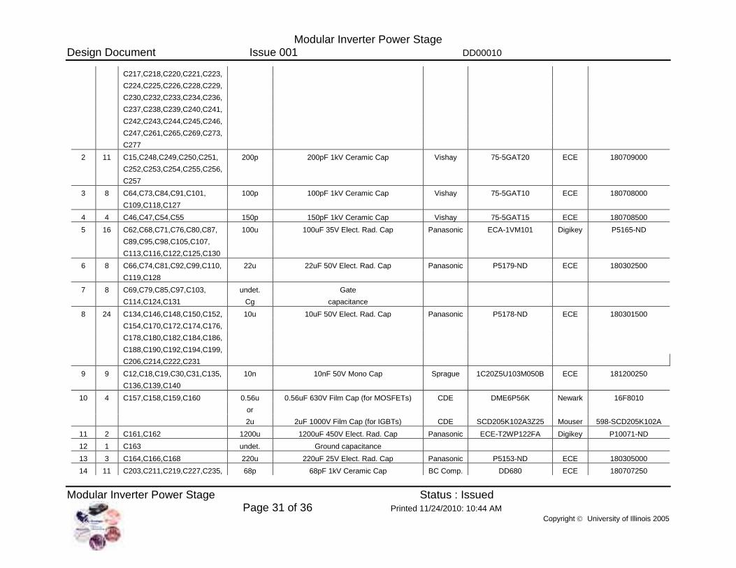
Modular Inverter Power Stage Design Document Issue 001 DD00010
Modular Inverter Power Stage Status : Issued Page 31 of 36 Printed 11/24/2010: 10:44 AM
Copyright University of Illinois 2005
C217,C218,C220,C221,C223,
C224,C225,C226,C228,C229,
C230,C232,C233,C234,C236,
C237,C238,C239,C240,C241,
C242,C243,C244,C245,C246,
C247,C261,C265,C269,C273,
C277
2 11 C15,C248,C249,C250,C251, 200p 200pF 1kV Ceramic Cap Vishay 75-5GAT20 ECE 180709000
C252,C253,C254,C255,C256,
C257
3 8 C64,C73,C84,C91,C101, 100p 100pF 1kV Ceramic Cap Vishay 75-5GAT10 ECE 180708000
C109,C118,C127
4 4 C46,C47,C54,C55 150p 150pF 1kV Ceramic Cap Vishay 75-5GAT15 ECE 180708500
5 16 C62,C68,C71,C76,C80,C87, 100u 100uF 35V Elect. Rad. Cap Panasonic ECA-1VM101 Digikey P5165-ND
C89,C95,C98,C105,C107,
C113,C116,C122,C125,C130
6 8 C66,C74,C81,C92,C99,C110, 22u 22uF 50V Elect. Rad. Cap Panasonic P5179-ND ECE 180302500
C119,C128
7 8 C69,C79,C85,C97,C103, undet. Gate
C114,C124,C131 Cg capacitance
8 24 C134,C146,C148,C150,C152, 10u 10uF 50V Elect. Rad. Cap Panasonic P5178-ND ECE 180301500
C154,C170,C172,C174,C176,
C178,C180,C182,C184,C186,
C188,C190,C192,C194,C199,
C206,C214,C222,C231
9 9 C12,C18,C19,C30,C31,C135, 10n 10nF 50V Mono Cap Sprague 1C20Z5U103M050B ECE 181200250
C136,C139,C140
10 4 C157,C158,C159,C160 0.56u 0.56uF 630V Film Cap (for MOSFETs) CDE DME6P56K Newark 16F8010
or
2u 2uF 1000V Film Cap (for IGBTs) CDE SCD205K102A3Z25 Mouser 598-SCD205K102A
11 2 C161,C162 1200u 1200uF 450V Elect. Rad. Cap Panasonic ECE-T2WP122FA Digikey P10071-ND
12 1 C163 undet. Ground capacitance
13 3 C164,C166,C168 220u 220uF 25V Elect. Rad. Cap Panasonic P5153-ND ECE 180305000
14 11 C203,C211,C219,C227,C235, 68p 68pF 1kV Ceramic Cap BC Comp. DD680 ECE 180707250

Modular Inverter Power Stage Design Document Issue 001 DD00010
Modular Inverter Power Stage Status : Issued Page 32 of 36 Printed 11/24/2010: 10:44 AM
Copyright University of Illinois 2005
C259,C263,C267,C271,C272,
C275
15 9 C258,C260,C262,C264,C266, 470p 470pF 1kV Ceramic Cap Vishay 75-5GAT47 ECE 180711000
C268,C270,C274,C276
16 5 D1,D2,D3,D6,D7 1N4742 1W 12V Zener Diode Fairchild 1N4742A ECE 30103750
16 40 D10,D11,D12,D13,D14,D15, MUR160 Rect. ultrafast, 600V, 1A axial Onsemi MUR160 Newark 08F2048
D16,D17,D18,D19,D20,D21, or
D22,D23,D24,D25,D26,D27, 1N4148 70V Diode Fairchild 1N4148 ECE 30157300
D28,D29,D30,D31,D32,D33,
D34,D35,D36,D37,D38,D39,
D40,D41,D42,D43,D44,D45,
D46,D47,D48,D49
17 10 D50,D51,D52,D53,D54,D55, 1N4740 1W 10V Zener Diode Motorola 1N4740A ECE 30103250
D56,D57,D58,D59
18 1 JP1 2 pos. double row header Berg 54102-S08-02 ECE 300430200
19 1 J1 34 pin straight solder header 3M Corp. 3431-6002 ECE 300307750
20 1 J2 26 pin straight solder header 3M Corp. 3429-6002 ECE 300307500
21 8 J3,J4,J5,J6,J7,J8,J9,J10 Gate signals connectors
22 1 J11 MTA100-6 6 pos MTA100 header AMP 571-6404566 ECE 300361300
23 1 J12 CON14A CPLD prog. conn., 14pin, 2mm Molex 87331-1420 Digikey WM18063-ND
24 45 J13,J14,J15,J16,J17,J18, AWG14 14 Gage wire
J19,J20,J21,J22,J23,J24, connector for
J25,J26,J27,J28,J29,J30, power wiring
J31,J32,J33,J34,J35,J36,
J37,J38,J39,J40,J41,J42,
J43,J44,J45,J46,J47,J48,
J60,J62,J63,J64,J65,J66,
J67,J68,J69
25 1 J49 MTA156-4 4 pos MTA156 header AMP 571-6404284 ECE 300361600
26 1 J59 MTA100-4 4 pos MTA100 header AMP 571-6404564 ECE 300361100
27 10 J50,J51,J52,J53,J54,J55, MTA100-3 3 pos MTA100 header AMP 571-6404563 ECE 300361000
J56,J57,J58,J61
28 1 J70 Soldering connection for GND re-routing
29 8 Q1,Q2,Q3,Q4,Q5,Q6,Q7,Q8 MOSFET, 150V, 105A IRF IRFPS3815 Newark 74C9925

Modular Inverter Power Stage Design Document Issue 001 DD00010
Modular Inverter Power Stage Status : Issued Page 33 of 36 Printed 11/24/2010: 10:44 AM
Copyright University of Illinois 2005
MOSFET, 500V, 46A IRF IRFPS40N50L Newark 74C9926
4 IGBT, dual module, 600V, 100A Eupec BSM100GB60DLC Mouser 641-
BSM100GB60DLC
30 4 RN1,RN2,RN3,RN4 1k8 DIP 8x1.8kOhm isolated res, DIP14 Bourns 4114R-1-182 Mouser 652-4114R-1-1.8K
31 1 RN5 100 SIP 100Ohm bussed res, SIP10 Bourns 4310R-1-101-ND ECE 150260000
32 1 RN6 10k SIP 10kOhm bussed res, SIP10 Bourns 4310R-1-103-ND ECE 150262000
33 2 RT1,RT2 NTC Current Limiter Inrush, 2.8A, 5Ohm Thermom. CL-160 Digikey KC016L-ND
34 18 R21,R22,R37,R38,R51, 10k 10kOhm res, 1%, 0.25W Yageo ECE 150103000
R52,R53,R54,R55,R56,R57,
R58,R59,R60,R61,R62,R95
36 12 R3,R7,R195,R196,R197, 4k99 4.99kOhm res, 1%, 0.25W Yageo ECE 150103000
R198,R199,R200,R201,R202,
R203,R204
37 5 R9,R23,R24,R39,R41 499k 499kOhm res, 1%, 0.25W Yageo ECE 150103000
38 13 R10,R19,R20,R35,R36,R100, 143 143Ohm res, 1%, 0.25W Yageo ECE 150103000
R101,R104,R107,R113,R114,
R116,R119
39 1 R13 24k3 24.3kOhm res, 1%, 0.25W Yageo ECE 150103000
40 4 R25,R27,R43,R44 43k2 43.2kOhm res, 1%, 0.25W Yageo ECE 150103000
41 8 R63,R67,R71,R75,R79,R83, 100 100Ohm res, 1%, 0.5W Xicon 273-100 Mouser 273-100
R87,R91
42 8 R64,R68,R72,R76,R80,R84, undet. GD power resistance, 1%, 0.5W
R88,R92 Rc
43 8 R65,R69,R74,R78,R82,R85, Rg 15.0Ohm res, 1%, 0.5W Xicon 273-15-RC Mouser 273-15-RC
R90,R93 or
47.5 Ohm res, 1%, 0.25W Yageo ECE 150103000
44 8 R66,R70,R73,R77,R81,R86, 47k5 47.5kOhm res, 1%, 0.5W Xicon 273-47.5K Mouser 273-47.5K
R89,R94
45 14 R102,R108,R111,R117,R125, 200 200Ohm res, 1%, 0.25W Yageo ECE 150103000
R131,R139,R145,R153,R159,
R167,R173,R181,R187
46 58 R1,R2,R4,R5,R6,R8,R11, 1k 1kOhm res, 1%, 0.25W Yageo ECE 150103000
R14,R15,R16,R17,R18,R26,

Modular Inverter Power Stage Design Document Issue 001 DD00010
Modular Inverter Power Stage Status : Issued Page 34 of 36 Printed 11/24/2010: 10:44 AM
Copyright University of Illinois 2005
R28,R31,R32,R33,R34,R40,
R42,R47,R48,R49,R50,R96,
R97,R98,R99,R103,R105,
R106,R109,R110,R112,R115,
R118,R123,R124,R129,R135,
R137,R138,R143,R149,R151,
R152,R157,R163,R165,R166,
R171,R177,R179,R180,R185,
R191,R193,R194
47 10 R128,R134,R142,R148,R156, 1k Pot 1k Trim Pot, 25 turn Bourns 3296W-1-102 ECE 150340600
R162,R170,R176,R184,R190
48 3 R120,R121,R122 undet. Ground resistance, 0.25W
49 20 R126,R127,R130,R133,R140, Rv 124kOhm res, 1%, 0.25W Yageo ECE 150103000
R141,R144,R147,R154,R155, or
R158,R161,R168,R169,R172, 499kOhm res, 1%, 0.25W Yageo ECE 150103000
R175,R182,R183,R186,R189
50 10 R12,R132,R136,R146,R150, 6k81 6.81kOhm res, 1%, 0.25W Yageo ECE 150103000
R160,R164,R174,R178,R188,
R192
51 4 SW1,SW2,SW3,SW4 3-pos. DIP switch, SPST Grayhill 76SB03 Newark 28F1451
52 1 SW5 8-pos. DIP switch, SPST Grayhill 76SB08 ECE 240120500
53 32 TP1,TP3,TP4,TP5,TP6,TP19, TP white Testpoint white Keystone 5012 ECE
TP20,TP21,TP22,TP23,TP24,
TP25,TP26,TP27,TP28,TP29,
TP30,TP31,TP32,TP33,TP34,
TP35,TP36,TP37,TP38,TP39,
TP40,TP41,TP42,TP43,TP44,
TP45
54 10 TP2,TP7,TP8,TP9,TP10, TP yellow Testpoint yellow Keystone 5014 ECE
TP68,TP69,TP70,TP71,TP72
55 24 TP11,TP12,TP13,TP14,TP15, TP orange Testpoint orange Keystone 5013 ECE
TP16,TP17,TP18,TP73,TP74,
TP75,TP76,TP77,TP78,TP79,
TP80,TP85,TP86,TP87,TP88,
TP89,TP90,TP91,TP92

Modular Inverter Power Stage Design Document Issue 001 DD00010
Modular Inverter Power Stage Status : Issued Page 35 of 36 Printed 11/24/2010: 10:44 AM
Copyright University of Illinois 2005
56 6 TP46,TP47,TP48,TP49,TP50, TP red Testpoint red Keystone 5010 ECE
TP51
57 20 TP52,TP53,TP54,TP55,TP56, TP black Testpoint black Keystone 5011 ECE
TP57,TP58,TP59,TP60,TP61,
TP62,TP63,TP64,TP65,TP66,
TP67,TP81,TP82,TP83,TP84
58 2 U1,U3 Precision Centigrade Temp Sensor, TO-
92 National LM35CZ Newark 92F287
59 16 U2,U4,U7,U9,U11,U13,U15, Dual Opamp, JFET Input, 8-DIP TI TLE2082ACP Newark 26C1841
U20,U22,U24,U26,U44,U46,
U48,U50,U52
60 9 U5,U8,U10,U12,U14,U54, Comparator, single, 8-DIP National LM311N ECE 90111500
U55,U56,U57
61 1 U6 Quad SPST, N.O., 16-DIP MAXIM DG212CJ Newark 90C1245
62 3 U16,U17,U18 Quad Opamp, JFET Input, 14-DIP TI TL2084CN Newark 08F9183
63 4 U19,U21,U23,U25 Current Transducer, CL, 100A nom LEM LAH 100-P Digikey 398-1009-ND
or
Current Transducer, CL, 25A nom LEM LAH 25-NP Digikey 398-1007-ND
64 8 U27,U28,U29,U30,U31,U32, Octocoupler Gate Drive, 2A, 16-SOIC Agilent HCPL-316J Newark 92F648
U33,U34
65 1 U35 CPLD 84-PLCC Xilinx XC95108-15PC84C Digikey 122-1175-ND
66 1 U36 Voltage Supervisor, 8-DIP TI TLC7705IP Newark 66F4591
67 1 U37 Quad Diff. Line Driver, 16-DIP National DS26LS31CN Newark 07B5238
68 1 U38 20MHz 5V 14-DIP Oscillator Mouser 520-TCF2000 ECE 140111000
69 3 U39,U40,U41 Quad Diff. Line Receiver, 16-DIP National DS26LS32ACN Newark 07B5239
70 2 U42,U43 Hex Inverter IC, 14-DIP TI SN74LS04N ECE 90501250
71 5 U45,U47,U49,U51,U53 Isolated Voltage Amplifier, 8-DIP Agilent HCPL-7800A Newark 06F5493
72 1 U35 PLCC Socket, 84 pos, through hole Mill-Max 940-99-084-24-
000000 Mouser 575-842494
73 1 JP1 Mini Jump Jumpers 0.1" Berg 65474-010 ECE 300425000
74 4 SW1,SW2,SW3,SW4 Solder Socket 6 pin, 6-DIP Rob.-Nug. ICE-063-S-TG Mouser 517-ICE-063-S-TG
75 31 U2,U4,U5,U7,U8,U9,U10, Solder Socket 8 pin, 8-DIP Rob.-Nug. ICE-083-S-TG ECE 360120000
U11,U12,U13,U14,U15,U20,
U22,U24,U26,U36,U44,U45,
U46,U47,U48,U49,U50,U51,

Modular Inverter Power Stage Design Document Issue 001 DD00010
Modular Inverter Power Stage Status : Issued Page 36 of 36 Printed 11/24/2010: 10:44 AM
Copyright University of Illinois 2005
U52,U53,U54,U55,U56,U57
76 5 U16,U17,U18,U42,U43 Solder Socket 14 pin, 8-DIP Rob.-Nug. ICE-143-S-TG ECE 360120250
77 10 RN1,RN2,RN3,RN4,SW1, Solder Socket 16 pin, 8-DIP Rob.-Nug. ICE-163-S-TG ECE 360120500
U6,U37,U39,U40,U41
78 15 4-40x1" Nylon Spacer Smith 4062 ECE 820158400
79 12 4-40x1" Brass Hex Spacer Smith 2334 ECE 830145750
80 30 4-40x1/4" Nylon Screw McMaster 95000A106 ECE 830710500
81 10 3 pos MTA100 Housing Amp 571-6404403 ECE 300360100
82 1 4 pos MTA100 Housing Amp 571-6404404 ECE 300360200
83 1 4 pos MTA156 Housing Amp 571-6404284 ECE 300361600
Grainger Center for Electric Machinery and Electromechanics Department of Electrical and Computer Engineering
University of Illinois at Urbana-Champaign 1406 W. Green St.
Urbana, IL 61801
The information contained in this Document and the Appendices may not be copied, reproduced, distributed or stored in a retrieval system without the prior express written permission of the author.
Copyright Board of Trustees of the University of Illinois 2005. All Rights Reserved
Design Document
Modular Inverter Isolated Power Supply
Reference: DD00011
Issue: 001
Status: Issued
Author: Zakdy Sorchini
Updated: Ali M. Bazzi / Kieran Levin
Principal Investigator: Jonathan Kimball
Created: March 6, 2006
Updated: Nov. 23, 2010
\\cts-file-02\power\DesignArchives\Documents\Design Documents\DD00011-001 Modular Inverter Isolated Power Supply.doc
Abstract:
This document briefly describes the functionality and characteristics of the isolated power supplies
for the power stage. A push-pull forward converter with sensorless current mode control is
implemented.
Modular Inverter Isolated Power Supply Design Document Issue 001 DD00011
Modular Inverter Isolated Power Supply Status : Issued Page 2 of 6 Printed 11/24/2010: 10:45 AM
Copyright University of Illinois 2005
Document Revision History
Issue Date Comments
000 4/3/2006 Initial release. 001 11/23/2010 Documentation for new isolated power supply added.
Contents
1. Introduction ......................................................................................................... 3
1.1 Scope ..................................................................................................................................... 3
1.2 References ............................................................................................................................. 3
1.3 Known Issues ......................................................................................................................... 3
2. Interface .............................................................................................................. 3
2.1 Input Power ............................................................................................................................ 3
2.2 Output Power ......................................................................................................................... 4
3. Power Circuit ...................................................................................................... 4
4. Control Circuit ..................................................................................................... 4
5. New Isolated Power Supply ................................................................................ 5
5.1 Technical Specifications ......................................................................................................... 5
5.2 Schematic............................................................................................................................... 5
5.3 Board Layout .......................................................................................................................... 6
5.4 Testing Procedure .................................................................................................................. 6

Modular Inverter Isolated Power Supply Design Document Issue 001 DD00011
Modular Inverter Isolated Power Supply Status : Issued Page 3 of 6 Printed 11/24/2010: 10:45 AM
Copyright University of Illinois 2005
1. Introduction
The isolated power supplies are used to power the gate drive circuit of the Power Stage, for both
IGBT and MOSFET versions. It provides loosely regulated gate drive voltage and regulated logic
voltage. The power supplies implement a push-pull forward converter using sensorless current
mode control.
Note: This power supply is no longer used due to several hardware failures. Section 5 presents a
newer more reliable design.
1.1 Scope
The isolated power supplies are intended to be part of the modular inverter, used with the power
stage board. They can also be used for other gate drive circuits or circuits that required minimum
power. Primary used is for research.
1.2 References
Schematic: SK0032 rev 2
Layout: PB0032 rev B
Power stage board: SK0031 and PB0031
1.3 Known Issues
There is no output short-circuit protection. The MOSFETs or the current-limiting resistors will fail
during an output short-circuit.
There is no soft-start in the original design. The circuit was modified to provide some degree of
soft-start, but this is very dependent on the voltage source used to feed the power supply.
The schematic and PCB, as archived and manufactured, have to be modified to implement the
power supplies. All the details of the modifications are included in the schematic.
The sensorless current mode control seems to give two different steady-state behaviors for the
power supplies. The primary sided current can be at the intended frequency, or at double the
intended frequency. The actual steady-state behavior for a given power supply seemed to be always
the same, but among power supplies seems to be random.
2. Interface
2.1 Input Power
The power supplies require ±15 V only. Logic power is internally created, because it is required to
be referenced to the -15 V rail. The input power connector is an MTA-100 (J1).

Modular Inverter Isolated Power Supply Design Document Issue 001 DD00011
Modular Inverter Isolated Power Supply Status : Issued Page 4 of 6 Printed 11/24/2010: 10:45 AM
Copyright University of Illinois 2005
2.2 Output Power
The power supplies produce +15 V (Zener regulated) and -5 V (nominal, unregulated) and +5V
regulated. The +15 and -5 V are used for the gate drive power. The +5V is used to power the actual
gate drive IC. The output power connector is an MTA-100 (J2).
3. Power Circuit
The power supply is based on a push-pull forward converter. The full 30 V input voltage is applied
to the transformer. This requires the gate drive circuit to be referenced to the -15 V rail. IRF630
MOSFETs are used (can substitute accordingly, recall that the MOSFETS should be able to block
at least 60 V not considering overshoot). Output diodes are MBR1100 Schottky.
The output of the forward converter (nominally 20 V) is regulated to +15 V with a Zener diode.
The Zener anode is the output common. The remaining part of the 20 V is the negative gate drive
voltage. The +15 V is then fed to a 7805 regulator for logic power.
4. Control Circuit
The control circuit generates the required gate drive signals to operate the converter. First, the
transformer input voltage is integrated (the integration time constant is adjustable to provide some
control over the switching frequency). This “control voltage” is then compared to fixed positive
and negative voltages. When the control voltage exceeds the reference, a latch is SET or RESET to
keep the flux inside an hysteresis band.
The latch directly controls a MIC4428 buffer that in turn controls the gates of the MOSFETs. The
gate voltage is 5 V. No deadtime is provided by the gate driver. Deadtime is achieved by using
diodes in the gate path and using asymmetric resistance for turn-on and turn-off.
In general, it is possible to use a 100 kHz switching frequency, but 50 kHz is recommended. (Each
individual power supply must be adjusted and monitored for saturation. If saturation occurs, raise
the switching frequency. This is required because two different steady-state behaviors were
observed during calibration.)
Modular Inverter Isolated Power Supply Design Document Issue 001 DD00011
Modular Inverter Isolated Power Supply Status : Issued Page 5 of 6 Printed 11/24/2010: 10:45 AM
Copyright University of Illinois 2005
5. New Isolated Power Supply
The isolated power supplies are designed to provide power for the gate and logic circuits for the high
and low side MOSFET/IGBT drivers in the modular inverter. The old design was changed because it
suffered from frequent failures and was extremely sensitive to failures on the power stage. Relay RL1 of
the original isolated power supply was replaced with a 2.7 Ω resistor that acted as a fuse when an over-
current occurred on the supply. This needed replacement whenever it was blown up. Five power supplies
are needed for the inverter: one for the lower gate drivers of all four outputs (in the middle of the five
supplies), and four individual supplies for each of the four high-side gate drivers.
5.1 Technical Specifications
The new design uses a standard isolated dc – dc converter TWR-5/1000-15/200-D24A with a high
level of isolation. Our inverter uses a 300V rail, so for a factor of double the rating (for safety) we should
use an isolation level of at least 600V. The next lowest isolation part we can get is 1000V. The datasheet
of this design is found at the end of this document.
5.2 Schematic
The circuit board provides connectors, a small load resistor which should be populated for all high-
side gate-driver supplies (4) and a -5V regulator which is not offered as an output by the isolated power
supply. The schematic of the new design is shown in Figure 1.
Figure 1. Schematic of the new isolated power supply

Modular Inverter Isolated Power Supply Design Document Issue 001 DD00011
Modular Inverter Isolated Power Supply Status : Issued Page 6 of 6 Printed 11/24/2010: 10:45 AM
Copyright University of Illinois 2005
5.3 Board Layout
The board layout is shown in Figure 2. The following components in Figure 2 are detailed here:
IC1: 7905 voltage regulator.
R1: 200Ω 1/4W. This is only installed when the +5V output of the supply is used, i.e., with the supply
powering the low side of the drivers.
C1: 20μF electrolytic capacitor.
C2: 47μF electrolytic capacitor.
C3, C4: 22μF electrolytic capacitor.
DATEL TWR-5/1000-15/200-D24A
Figure 2. Board layout of the new isolated power supply
5.4 Testing Procedure
1. Connect a bench power supply to X1 (input terminals) with the power off. Set a current limit of
300mA, turn on the supply output and slowly increase the voltage to 25 V. If at any time the
current is limiting, then there is a short in the supply. Turn off the supply and check for faults.
2. Measure each output pin in X2. Connect the negative pin of a voltmeter to pin 2. Measure pin 1
(15V ± 1V), pin 3 (-5V ± 0.2V), and pin 4 (+5 ± 0.2V). If pin 1 is out of range then R1 may not
be installed.

Software Development Guide for Modular Inverter Design Document Issue 003 TU0003
Design Document
Software Development Guide for Modular Inverter
Reference: TU0003
Issue: 003
Status: Issued V1.0
Author: Guoliang Zhang
Updated by: Ali M. Bazzi / Paul Rancuret
Principal Investigator: J. Kimball
Created: April 2, 2005
Updated: November 23, 2010
Abstract:
This document is intended to archive the modular inverter control software architecture, which is
based on Matlab/Simulink Embedded Coder for TI C2000 toolbox. Some customized functions are
described in detail.
This document also serves as instruction manual for power lab users that may use the modular
inverter to develop digital motor control algorithms or other related applications. A fully functional
example is included at the end of this document and links to the related files are provided.
Some useful resources are listed in the appendix to help users locate necessary knowledge base that
are required to fulfill advanced functionalities.

Software Development Guide for Modular Inverter Design Document Issue 003 TU0003
Document Revision History
Issue Date Comments
001 2/17/2006 First release 002 3/3/2006 Added Flash part, updated TOC 003 11/23/2010 Added Recommendations for Advanced Applications
Contents
1. Introduction ......................................................................................................... 3
1.1 Overview and Scope .............................................................................................................. 3
1.2 Definitions............................................................................................................................... 5
1.3 References ............................................................................................................................. 5
2. User Interface ..................................................................................................... 6
2.1 Matlab/Simulink Environment Setup ...................................................................................... 6
2.2 Developing Control Model in Simulink ................................................................................... 9
2.2.1 Fixed Point Datatype ......................................................................................................... 9
2.2.2 IQ Math Library and DMC Library ................................................................................... 11
2.2.3 Simulation ....................................................................................................................... 12
2.2.4 Integrate I/Os and core functions of the DSP into the control ........................................ 12
2.3 Generate Code and Run It on DSP ..................................................................................... 13
2.4 Errors, Faults and Exceptions .............................................................................................. 13
2.4.1 Board name mismatch .................................................................................................... 13
2.4.2 Could not find target board ............................................................................................. 13
2.4.3 Model contains ADC blocks won’t work under internal memory mode........................... 14
2.4.4 Over-run detected ........................................................................................................... 14
3. A Step-by-Step Example ................................................................................... 15
4. Create Flash Based Project .............................................................................. 16

Software Development Guide for Modular Inverter Design Document Issue 003 TU0003
1. Introduction
1.1 Overview and Scope
EZdsp2812 is a board made by Spectrumdigital.com that utilizes a TI TS320F2812 DSP core. Full
description on this chip can be found at TI.com. Some of the key features of this DSP controller
are:
Extended Temperature Performance of
−55C to 125C
Three 32-Bit CPU-Timers
128-Bit Security Key/Lock − Protects Flash/ROM/OTP and L0/L1 SARAM − Prevents Firmware Reverse Engineering
High-Performance Static CMOS Technology
− 150 MHz (6.67-ns Cycle Time) − Low-Power (1.8-V Core @135 MHz, 1.9-V Core @150 MHz, 3.3-V I/O) Design Motor Control Peripherals
− Two Event Managers (EVA, EVB) − Compatible to 240xA Devices
JTAG Boundary Scan Support
High-Performance 32-Bit CPU (320C28x) − 16 x 16 and 32 x 32 MAC Operations − 16 x 16 Dual MAC − Harvard Bus Architecture − Atomic Operations − Fast Interrupt Response and Processing − Unified Memory Programming Model − 4M Linear Program/Data Address Reach − Code-Efficient (in C/C++ and Assembly) − 320F24x/LF240x Processor Source Code Compatible
Serial Port Peripherals − Serial Peripheral Interface (SPI) − Two Serial Communications Interfaces (SCIs), Standard UART − Enhanced Controller Area Network (eCAN) − Multichannel Buffered Serial Port (McBSP)
12-Bit ADC, 16 Channels − 2 x 8 Channel Input Multiplexer − Two Sample-and-Hold − Single/Simultaneous Conversions − Fast Conversion Rate: 80 ns/12.5 MSPS
On-Chip Memory − Flash Devices: Up to 128K x 16 Flash (Four 8K x 16 and Six 16K x 16 Sectors) − ROM Devices: Up to 128K x 16 ROM − 1K x 16 OTP ROM − L0 and L1: 2 Blocks of 4K x 16 Each Single-Access RAM (SARAM) − H0: 1 Block of 8K x 16 SARAM − M0 and M1: 2 Blocks of 1K x 16 Each SARAM
Up to 56 General Purpose I/O (GPIO) Pins
Development Tools Include − ANSI C/C++ Compiler/Assembler/Linker
− Code Composer StudioIDE
− DSP/BIOS
External Interface (2812) − Up to 1M Total Memory − Programmable Wait States − Programmable Read/Write Strobe Timing − Three Individual Chip Selects
Boot ROM (4K x 16) − With Software Boot Modes − Standard Math Tables

Software Development Guide for Modular Inverter Design Document Issue 003 TU0003
Code Composer Studio (CCS) for C2000 is the software development tool for this DSP. Current
version is V2.21. It is recommended to have only one CCS installed on one computer to avoid any
confliction between applications.
Matlab/Simulink provides the automated code generating tool for this DSP family. Users can
communicate with the DSP via Matlab Link for CCS. Under most cases, users should develop their
control algorithms in Simulink and use the automatic RTW tool to generate/build/download the
code to target DSP and run the executable program in CCS.
To use the digital controller system effectively and efficiently, certain skills/knowledge are
required. Based on the complexity that might get involved during the development, two levels of
users are defined:
Level 1: Control Algorithm developers
Example: motor control algorithm, digital pwm algorithm, filter designs, etc.
You need to have knowledge on
basic usage of Matlab/Simulink
fixed point data type, IQ math(just another form of fixed-point defined by TI)
discrete time signal processing -specifically, discrete time integration, sample/hold,
delay, Z transform.
PWM parameter settings
Hardware configuration on the modular inverter and its control board.
Matlab GUI is a plus
Real-Time multitask scheduling is a plus.
Level 2: Expanded function developers
Example: DAC, Communication, Stand alone applications, etc. Especially when your needs are
beyond the capability provided by our library functions.
Except requirements to level 1 users, you also need knowledge on
C/C++ and Library functions for C281x provided by TI.
S-Function in Matlab/Simulink
RTW(Real-Time Workshop) and TLC(Target Language Compiler)
Hardware on TI 320F2812 DSP is a plus.
This document focuses on level 1 user. References will be provided to help level 2 users locate the
necessary recourses.
A knowledge tree below shows the required skills/knowledge and their relationships for each group
of users. Bold text indicates key skill needed for that group of users. Real Time Data Transfer
function is only available with the update of CCS 2.20+ and Matlab R14 SP2+.
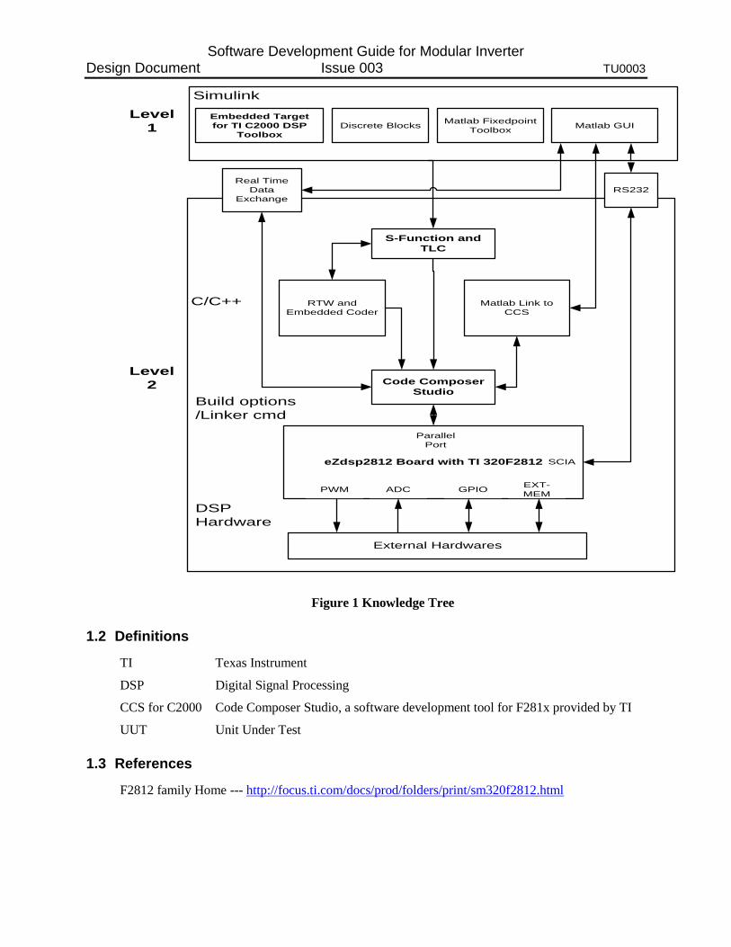
Software Development Guide for Modular Inverter Design Document Issue 003 TU0003
Embedded Target
for TI C2000 DSP
Toolbox
Matlab Link to
CCS
Matlab Fixedpoint
Toolbox
RTW and
Embedded Coder
S-Function and
TLC
Discrete Blocks
Real Time
Data
Exchange
Code Composer
Studio
eZdsp2812 Board with TI 320F2812
RS232
Matlab GUI
PWM
SCIA
Parallel
Port
ADC GPIOEXT-
MEM
Level
1
Level
2
External Hardwares
Simulink
C/C++
DSP
Hardware
Build options
/Linker cmd
Figure 1 Knowledge Tree
1.2 Definitions
TI Texas Instrument
DSP Digital Signal Processing
CCS for C2000 Code Composer Studio, a software development tool for F281x provided by TI
UUT Unit Under Test
1.3 References
F2812 family Home --- http://focus.ti.com/docs/prod/folders/print/sm320f2812.html

Software Development Guide for Modular Inverter Design Document Issue 003 TU0003
2. User Interface
2.1 Matlab/Simulink Environment Setup
User will develop control algorithm under Simulink environment. To successfully run the process,
several toolboxes are required. They are: Fixed Point Toolbox, RTW toolbox, Embedded Coder
toolbox and Embedded Coder for TI C2000 Toolbox. Type ―ver‖ at Matlab command window to
see if all of those toolboxes are installed on the computer you plan to work on. We have one license
for each toolbox for the whole group. Also, a Microsoft VC6.0 should be installed on the computer.
Upon opening the Simulink Library browser, an ―Embedded Target for TI C2000 DSP‖ item
should show up on the left, all the build-in functions can be found under this group of library
modules.
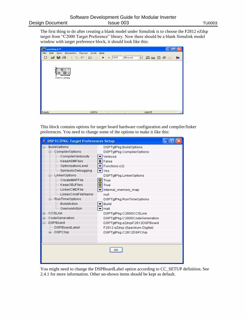
Software Development Guide for Modular Inverter Design Document Issue 003 TU0003
The first thing to do after creating a blank model under Simulink is to choose the F2812 eZdsp
target from ―C2000 Target Preference‖ library. Now there should be a blank Simulink model
window with target preference block, it should look like this:
This block contains options for target board hardware configuration and compiler/linker
preferences. You need to change some of the options to make it like this:
You might need to change the DSPBoardLabel option according to CC_SETUP definition. See
2.4.1 for more information. Other un-shown items should be kept as default.
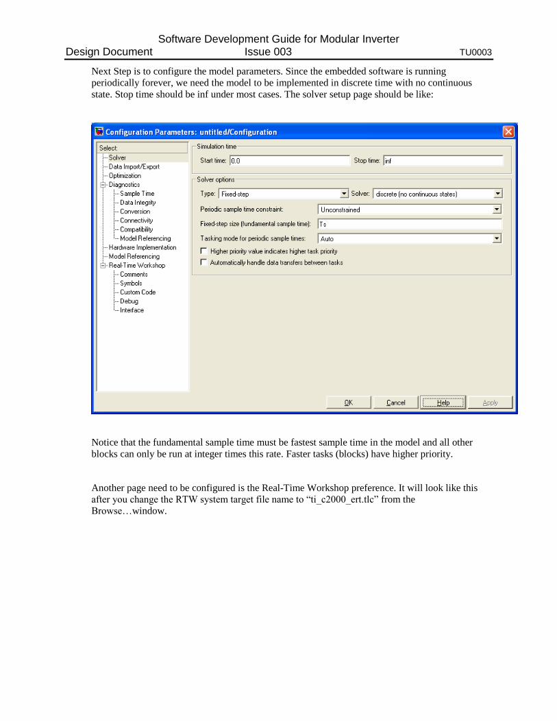
Software Development Guide for Modular Inverter Design Document Issue 003 TU0003
Next Step is to configure the model parameters. Since the embedded software is running
periodically forever, we need the model to be implemented in discrete time with no continuous
state. Stop time should be inf under most cases. The solver setup page should be like:
Notice that the fundamental sample time must be fastest sample time in the model and all other
blocks can only be run at integer times this rate. Faster tasks (blocks) have higher priority.
Another page need to be configured is the Real-Time Workshop preference. It will look like this
after you change the RTW system target file name to ―ti_c2000_ert.tlc‖ from the
Browse…window.

Software Development Guide for Modular Inverter Design Document Issue 003 TU0003
This finishes the configuration of the model. It is recommended to set the sampling color and data
type of each port display options on from the simulink model window toolbar \Format\Port and
Signal Displays option.
2.2 Developing Control Model in Simulink
In this part, we describe some key concept to build a control model.
2.2.1 Fixed Point Datatype
Assume you are familiar with the fixed point data concept. In Simulink, to assign certain datatype
to a specific block is done by changing signal/parameter settings in the block property tab. For
example, we want to use a 32bit fixed point gain of 3.14159, and want 1/100000 resolution on the
output within +/-2000. Then we need to setup the signal data type and parameter data type as:
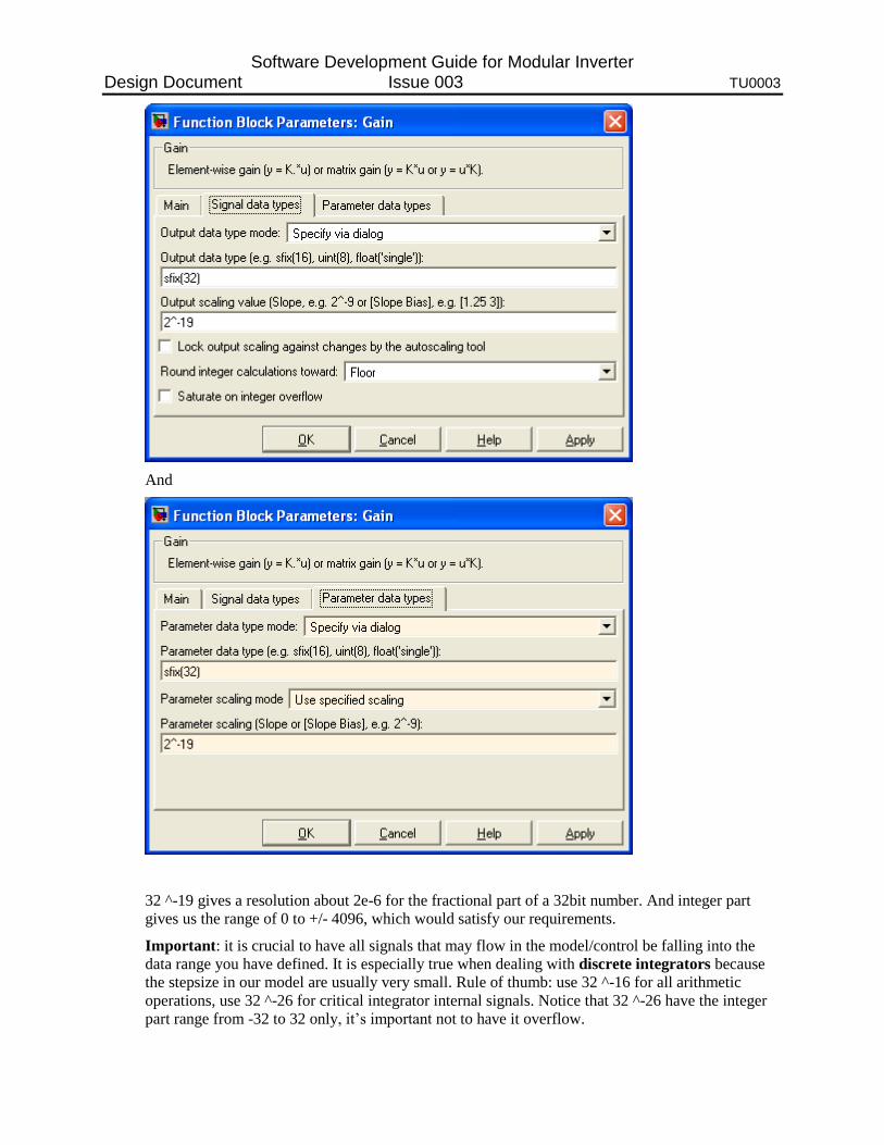
Software Development Guide for Modular Inverter Design Document Issue 003 TU0003
And
32 ^-19 gives a resolution about 2e-6 for the fractional part of a 32bit number. And integer part
gives us the range of 0 to +/- 4096, which would satisfy our requirements.
Important: it is crucial to have all signals that may flow in the model/control be falling into the
data range you have defined. It is especially true when dealing with discrete integrators because
the stepsize in our model are usually very small. Rule of thumb: use 32 ^-16 for all arithmetic
operations, use 32 ^-26 for critical integrator internal signals. Notice that 32 ^-26 have the integer
part range from -32 to 32 only, it‘s important not to have it overflow.

Software Development Guide for Modular Inverter Design Document Issue 003 TU0003
2.2.2 IQ Math Library and DMC Library
Under Simulink Library Browser, you can find C28x IQmath Library and DMC Library under
Embedded Target for TI C2000 DSP toolbox. These are functions that would generate much more
efficient code than using common Matlab blocks.
When choosing arithmetic operation blocks, you should always use the one from IQmath library
instead the ones from Simulink Block sets. For example, to implement a gain, instead of using the
gain from Simulin\Math Operations\Gain, you should use a constant with proper data type and an
IQN x IQN or other multiplication functions under IQmath Library. In the DMC Library, there are
transforms that have already been implemented in an integrated block format.
Some other functions like filters, discrete integrators should be implemented by blocks from
Simulink\Descrete library.
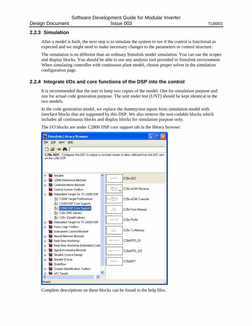
Software Development Guide for Modular Inverter Design Document Issue 003 TU0003
2.2.3 Simulation
After a model is built, the next step is to simulate the system to see if the control is functional as
expected and we might need to make necessary changes to the parameters or control structure.
The simulation is no different than an ordinary Simulink model simulation. You can use the scopes
and display blocks. You should be able to use any analysis tool provided in Simulink environment.
When simulating controller with continuous plant model, choose proper solver in the simulation
configuration page.
2.2.4 Integrate I/Os and core functions of the DSP into the control
It is recommended that the user to keep two copies of the model: One for simulation purpose and
one for actual code generation purpose. The unit under test (UNT) should be kept identical in the
two models.
In the code generation model, we replace the dummy/test inputs from simulation model with
interface blocks that are supported by this DSP. We also remove the non-codable blocks which
includes all continuous blocks and display blocks for simulation purpose only.
The I/O blocks are under C2800 DSP core support tab in the library browser.
Complete descriptions on these blocks can be found in the help files.

Software Development Guide for Modular Inverter Design Document Issue 003 TU0003
2.3 Generate Code and Run It on DSP
If all the software/toolboxes are installed properly and board configuration is correct, by clicking
on the ―build‖ button on top of the Simulink window, an automated process would be invoked and
the code should have been built in CCS. Then an active CCS project should appear on the left side
project manager window. In theory, the processor needs to be reset before loading the code into the
target DSP. In practice, it might not be necessary. To load and run the program, select File/Load
Program… from CCS main window, the modelname.out executable file usually appears by default.
Otherwise, you should be able to locate it manually under modelname_c2000_rtw/ directory. After
the code is loaded in the DSP successfully, press F5 or choose ―run‖ button to run the program on
the target. If the target stops immediately after a run command, you might need to do File/Reload
Program… and run it again. The code generation may take around 1-2 minutes depending on the
complexity of the model and the computer you are using.
Explanations on some terms in this stage:
Generate Code: Matlab Target Language Compiler (TLC) to compile the Simulink model into C
code and other resources needed by later process.
Create CCS Project: Matlab TLC creates a project file and include all necessary resources into the
modelname_c2000_rtw directory.
Build: CCS C compiler is invoked to compile the project source files into .obj files.
Link: CCS Linker links all .obj files, library files from TI library into one executable
modelname.out file.
Load: CCS loader load the modelname.out file to the RAM on DSP according to the linker
command file modelname.cmd, which was generated by Matlab during ―Generate Code‖ stage.
2.4 Errors, Faults and Exceptions
Some common errors, faults, exceptions and their possible causes are presented in this section.
2.4.1 Board name mismatch
Symptom: After clicking the ―Build‖ button, error message saying board name not matching the
label defined in Target Preference Block.
Cause: Board name defined in target preference block is different than that from CC_setup.
Solution: Change the target preference board information to whatever indicated by error message.
2.4.2 Could not find target board
Symptom: After clicking the ―Build‖ button, error message saying cannot find board.
Cause: May caused by power loss on the target when Matlab is still running.
Solution: Make sure the power is connected to the board then reset the board from CCS
Debug/Reset Emulator. Then go to Matlab command window and type >> clear CCS_Obj.

Software Development Guide for Modular Inverter Design Document Issue 003 TU0003
2.4.3 Model contains ADC blocks won’t work under internal memory mode
Symptom: Loading error in CCS. Or the program is not running as expected if ADC is used and
internal memory mode is selected in target preference block.
Cause: Bug in Matlab when generating the model.cmd file. A DSECT is declared to a section that
would be used in ADC initialization. A DSECT-ed code section will not be loaded to the DSP
RAM by the loader.
Solution: 2 ways, either one will work:
1, go to C:\MATLABroot\toolbox\rtw\targets\tic2000\tic2000\src and open DSP281x_usDelay.asm
file with any text editor, comment out the line of .sect "ramfuncs" with ―;‖.
2: go to C:\MATLABroot\toolbox\rtw\targets\tic2000\tic2000 and open ti_c2800_cmd.tlc with any text editor, find the line of:
ramfuncs : > PRAMH0, PAGE = 0, TYPE = DSECT
Cross out the ―, TYPE = DSECT‖ part of this line. So it looks like: ramfuncs : > PRAMH0, PAGE = 0
2.4.4 Over-run detected
Symptom: After several tries of clicking the ―run‖ button, the program goes to ―Halt‖ position
repetitively.
Cause: Over-run is detected, CPU overloaded.
Solution: Increase the stepsize in the model and recompile. Make sure that there are no unnecessary
double precision or non-lookup-table type trigonometric functions in the model.
3. Recommendations for Advanced Applications
3.1 ADC and RTDX Issues
The number of ADC and RTDX channels in a Simulink block diagram affects that maximum
allowable sampling rate (Ts) that can be used on the DSP. The ADC has two main ports, A and B,
each having eight channels. While the maximum allowable rates are given in the eZdspF2812
datasheet, these do not reflect actual implementations in advanced applications that require
significant processing. It is advised that the minimum number of ADC channel is used to achieve
higher sampling rates. The reason this is true is that every ADC port, i.e., A or B, has a
multiplexed structure. This means that the multiplexer needs enough time to fetch ADC data for
the DSP to process it appropriately.
A similar problem exists with RTDX channels, and sampling rates might be even slower in this
case. RTDX channels communicate in real time between the DSP registers and MATLAB, thus
significant lag exists between on these hardware-software interface channels. Higher sampling
rates can be achieved with less RTDX channels.

Software Development Guide for Modular Inverter Design Document Issue 003 TU0003
When the sampling rate is high compared to what the DSP can handle for a given number of ADC
and RTDX channels, a block diagram might still compile without errors or warnings. But, when it
is run using Code Composer Studio or a MATLAB GUI, the DSP will crash. This can be noticed
with the ―Enable‖ LED flashes (this LED is on the power stage front panel). A recommended
practice is to start with a relatively low sampling rate, if possible for a given application, and then
increasing the rate until reaching the sampling limit.
Note that an essential step in building a Simulink block diagram using the real-time workshop is
that sampling rates should be multiples of each other. Down sampling and over sampling a signal
is always possible with the ―rate transition‖ Simulink blocks if this step is obeyed.
Sampling might pose to be a problem when high sampling rates are required, e.g., having an
estimation loop that is significantly faster than the controller.
For ADCs, signal-to-noise-ratio (SNR) is a very sensitive factor that needs to be considered
especially in advanced applications such as ripple-based control. SNR can be enhanced with
appropriate communication cable wiring and filtering — analog filtering on the control board and
digital filtering on the DSP.
3.2 Memory
The flash memory on the eZDSP TMS320F2812 DSP is limited to 128K words. In most
applications, this is plenty of program memory. However, with some advanced applications, it may
be very important to conserve memory as this limit is approached.
With field-oriented control of an induction motor, for example, it may be necessary to have many
embedded control laws to perform separate functions simultaneously using similar information.
Steps should be taken to ensure that the program does not have redundant calculations. For
instance, if two sections of your program need to know the currents in the d-q frame, have one
outside block of your program calculate these currents in the d-q frame, and use these values in
both sections. Do not have each section compute the d-q currents separately.
It is also very easy to use up memory words when filtering vector signals. It is recommended to
use the lowest order filter to achieve the goal, especially with vector signals. A second order filter
for a three-element vector uses much more memory than a first order filter.
Memory may also be saved by ensuring that constants are never stored more than once in memory.
For instance, if several pieces of your program require multiplication by 180, only store the number
180 once and refer to it by both blocks in the program. In Simulink, these means using only one
‗Constant‘ block for the number 180. You can then connect this single block to both subsystems
which need to use the value 180.
4. Examples
4.1 V/Hz Example
SW00025 folder contains documents (including this one) that are dedicated to the modular inverter
control software architecture, which is based on Matlab/Simulink Embedded Coder for TI C2000

Software Development Guide for Modular Inverter Design Document Issue 003 TU0003
toolbox. The eZdspLib.zip file contains the matlab code and model needed for Modular Inverter
dsp software generation and execution.
Extract the file to a folder that you are working under, and make sure this folder is included in the
matlab path setting. Keep the HyperTerminal file some where convenient for easy access. Navigate
in the matlab path selection tab and make the current work directory is your matlab
pth/eZdspLib/VperHzTest. Two models are provided. One is using Serial communication the other
is using RTDX communication. ezdsp2812_vphz32 is to be used with the HyperTerminal file you
extracted earlier. ezdsp2812_vphz32_wRTDX is used with .m file under the same directory.
4.2 Flux Estimation Example
Refer to the following paper for a summary of software and hardware requirements in a flux
estimation example using the modular inverter:
A.M. Bazzi and P.T. Krein, "Comprehensive Flux Estimator Implementation Procedures For
Advanced Control Of Inverter-Fed Induction Machines," How2Power Today Online
Magazine/Portal, June 2010.
5. Create Flash Based Project
SW00025 also contains a Flash_Based.zip file. It is the project that derived from V/Hz project in
the example but suitable to run as stand alone program.
To make a project generated from Matlab flashable. Follow the steps listed below:
i. Replace the .cmd file generated from Matlab/Simulink with the one in Fash_Based.zip
.cmd file. Change the file name to your project name.
ii. Add two files to the project by right click on project_name and choose Add files… in CCS:
coecsl.c and DSP281x_CodeStartBranch.asm
iii. Add one line in YourProjectName_main.c in main() so that it looks like:
void main(void)
init_COECSL(); // memcpy from Flash to RAM
init_board();
…
iv. Right click on project name, choose Build Option… click on Linker tab; change one of the
linker options from –cr to –c.
v. Change the jumper 7 position from 2-3 to 1-2 on the DSP board.
vi. Re-compile and build the project under CCS. DO NOT RECOMPILE UNDER
SIMULINK, OTHERWISE YOU LOSE ALL YOUR WORK.

Software Development Guide for Modular Inverter Design Document Issue 003 TU0003
vii. Instead of ―loading‖ your program to the RAM, now you need to use flash programmer
under CCS tools to burn the flash.
viii. After the process is done, reset the DSP and it should go.
NOTES:
1. All work in this chapter is not related to Matlab/Simulink any more. Work solely under CCS.
2. CCS software package that comes with the boards doesn‘t have a functional flash programmer.
Need to update the flash API patch, which can be obtained from c2000flashprogsw_v112.zip
under SW00025 directory. Or please check the latest version of CCS.
3. To save your work, change the directory name so that Matlab/Simulink won‘t erase it next time
you recompile your model. Move it to a safer place.
4. Don‘t forget to change the jumper back to its original position when done.
!!! important information for upgrading the system !!!
as of 24th of May 2006, two ezdsp systems has been upgrade the Matlab to R2006a.
several known problems and solutions:
1. CCS 3.1 is required. we have one on exchange drive.
2. some blocks not backward compatable. if there is an error (example the pwm blocks) or
warning, read carefully and replace the old block with new one. save your work before you
do so since once saved in later vresion, cannot go back easily.
3. internal mem map loading issue. if experience difficulty when loading the file in CCS, try
following:
open installationDir\toolbox\rtw\targets\tic2000\tic2000\ti_c281x_cmd.tlc
find the following text
...
%% Function: constructSectionAllocationx281xDSP ================================
%%
%function constructSectionAllocationx281xDSP() void
%openfile sectionAllocation
SECTIONS
codestart : > PRAMH0, PAGE = 0

Software Development Guide for Modular Inverter Design Document Issue 003 TU0003
.text : > PRAMH0, PAGE = 0
.cinit : > PRAMH0, PAGE = 0
ramfuncs : > PRAMH0, PAGE = 0
.reset : > RESET, PAGE = 0, TYPE = DSECT
%if (c2000ModelIRInfo.numRTDXs != 0)
.rtdx_text : > PRAMH0, PAGE = 0
%endif
...
add a line assigning memory for .pinit after .cinit assignment so it looks like
%% Function: constructSectionAllocationx281xDSP
================================
%%
%function constructSectionAllocationx281xDSP() void
%openfile sectionAllocation
SECTIONS
codestart : > PRAMH0, PAGE = 0
.text : > PRAMH0, PAGE = 0
.cinit : > PRAMH0, PAGE = 0
.pinit : > PRAMH0, PAGE = 0
ramfuncs : > PRAMH0, PAGE = 0
.reset : > RESET, PAGE = 0, TYPE = DSECT
%if (c2000ModelIRInfo.numRTDXs != 0)
.rtdx_text : > PRAMH0, PAGE = 0
%endif