Embed Size (px)
Citation preview
Modular Routing Design for Chiplet-based Systems
Jieming Yin* Zhifeng Lin† Onur Kayiran* Matthew Poremba*
Muhammad Shoaib Bin Altaf* Natalie Enright Jerger‡ Gabriel H. Loh*
*Advanced Micro Devices, Inc. †University of Southern California ‡University of Toronto
{jieming.yin, onur.kayiran, matthew.poremba, shoaib.altaf, gabriel.loh}@amd.com
[email protected] [email protected]
Abstract—System-on-Chip (SoC) complexity and the increas-ing costs of silicon motivate the breaking of an SoC into smaller“chiplets.” A chiplet-based SoC design process has the promiseto enable fast SoC construction by using advanced packag-ing technologies to tightly integrate multiple disparate chips(e.g., CPU, GPU, memory, FPGA). However, when assemblingchiplets into a single SoC, correctness validation becomes asignificant challenge. In particular, the network-on-chip (NoC)used within the individual chiplets and across chiplets to tiethem together can easily have deadlocks, especially if each chipis designed in isolation.
We introduce a simple, modular, yet elegant methodologyfor ensuring deadlock-free routing in multi-chiplet systems. Asan example, we focus on future systems combining chipletson an active silicon interposer. To maximize modularity, eachindividual chiplet is free to implement its own NoC topologyand local routing algorithm, and the interposer can implementits own independent topology and routing. Our methodologyimposes a few simple turn restrictions applied only to traffic asit flows into or out of the chiplets from the interposer, and weprovide a way to determine these restrictions. The end resultis an overall approach that enables highly-modular, chiplet-based SoC construction while eliminating deadlocks with highperformance.
Keywords-chiplet; deadlock-avoidance; routing
I. INTRODUCTION
The rising costs of large Systems-on-Chip (SoCs) in
increasingly complex process technologies are a motivation in
the design of SoCs based on “chiplets.” This concept breaks
a conventional monolithic SoC into several smaller chiplets,
each of which can be cheaper to develop, easier to reuse
across multiple products, and implemented with the most
appropriate process technology. The chiplet approach is being
actively worked on in academia [1]–[4], industry [5]–[11],
and government agencies [12].
There are many research and engineering challenges
associated with chiplet-based architectures; we focus on one
specific but critical problem. Adhering to a modular design
approach, each individual chiplet should be designed and
verified without any knowledge of the full system. When
constructing a SoC from multiple chiplets, even though
each individual component is properly verified, the fully-
integrated system may still have correctness issues. The
interconnection network is particularly vulnerable to this.
Each individual chiplet may contain its own local network-
on-chip (NoC) that is locally deadlock free and operates
properly for intra-chiplet traffic. However, connecting several
NoCs together can introduce new resource cycles that cause
cyclic dependencies across the chiplets.
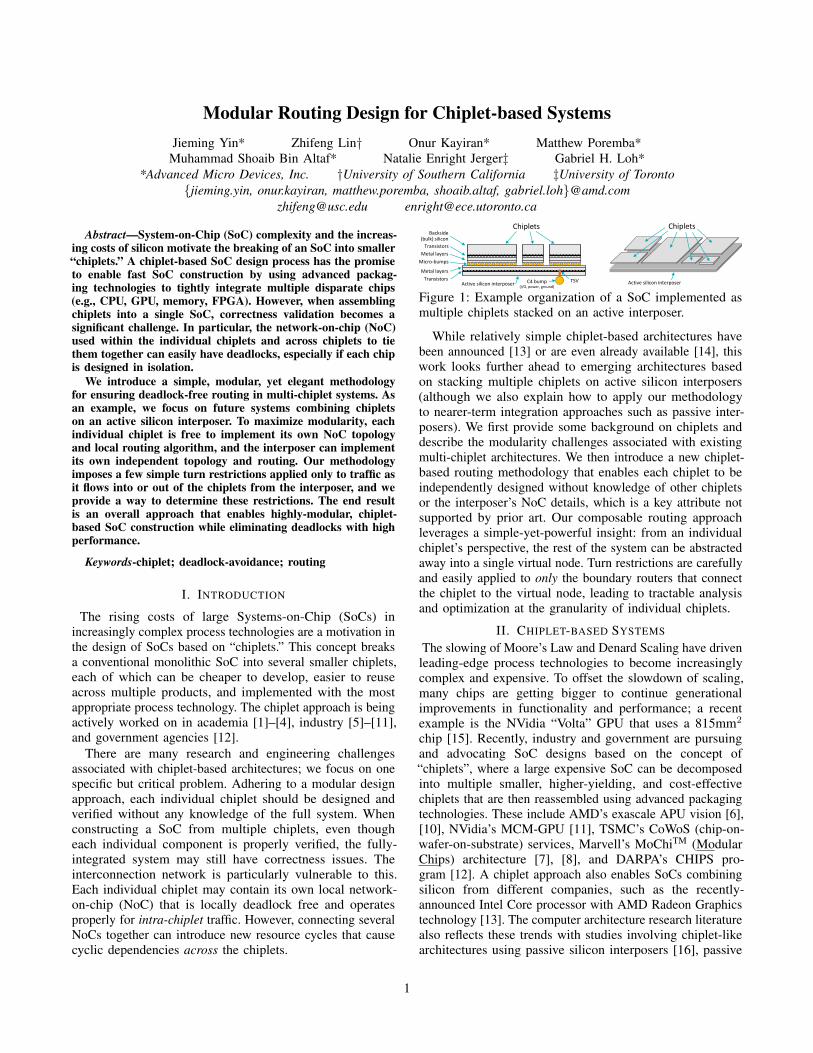
ChipletsBackside
(bulk) silicon
Transistors
Metal layers
Micro-bumps
Metal layers
Active silicon interposerTSVC4 bump
(I/O, power, ground)
Transistors
Chiplets
Active silicon interposer
Figure 1: Example organization of a SoC implemented as
multiple chiplets stacked on an active interposer.
While relatively simple chiplet-based architectures have
been announced [13] or are even already available [14], this
work looks further ahead to emerging architectures based
on stacking multiple chiplets on active silicon interposers
(although we also explain how to apply our methodology
to nearer-term integration approaches such as passive inter-
posers). We first provide some background on chiplets and
describe the modularity challenges associated with existing
multi-chiplet architectures. We then introduce a new chiplet-
based routing methodology that enables each chiplet to be
independently designed without knowledge of other chiplets
or the interposer’s NoC details, which is a key attribute not
supported by prior art. Our composable routing approach
leverages a simple-yet-powerful insight: from an individual
chiplet’s perspective, the rest of the system can be abstracted
away into a single virtual node. Turn restrictions are carefully
and easily applied to only the boundary routers that connect
the chiplet to the virtual node, leading to tractable analysis
and optimization at the granularity of individual chiplets.
II. CHIPLET-BASED SYSTEMS
The slowing of Moore’s Law and Denard Scaling have driven
leading-edge process technologies to become increasingly
complex and expensive. To offset the slowdown of scaling,
many chips are getting bigger to continue generational
improvements in functionality and performance; a recent
example is the NVidia “Volta” GPU that uses a 815mm2
chip [15]. Recently, industry and government are pursuing
and advocating SoC designs based on the concept of
“chiplets”, where a large expensive SoC can be decomposed
into multiple smaller, higher-yielding, and cost-effective
chiplets that are then reassembled using advanced packaging
technologies. These include AMD’s exascale APU vision [6],
[10], NVidia’s MCM-GPU [11], TSMC’s CoWoS (chip-on-
wafer-on-substrate) services, Marvell’s MoChiTM (Modular
Chips) architecture [7], [8], and DARPA’s CHIPS pro-
gram [12]. A chiplet approach also enables SoCs combining
silicon from different companies, such as the recently-
announced Intel Core processor with AMD Radeon Graphics
technology [13]. The computer architecture research literature
also reflects these trends with studies involving chiplet-like
architectures using passive silicon interposers [16], passive
1
DRAM
DRAM
DRAM
DRAM
DRAM
DRAM
DRAM
DRAM
CPU chiplet
GPU chiplet
CU/L1 CU/L1 CU/L1 CU/L1
CU/L1 CU/L1 CU/L1 CU/L1
CU/L1 CU/L1 CU/L1 CU/L1
CU/L1 CU/L1 CU/L1 CU/L1
GPU L2 GPU L2
GPU L2 GPU L2
GPU L2 GPU L2
GPU L2 GPU L2
CPU CPU
CPU CPU
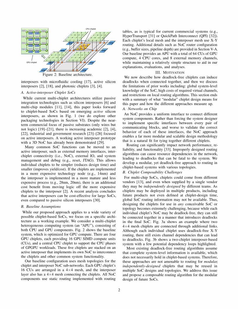
Figure 2: Baseline architecture.
interposers with microfluidic cooling [17], active silicon
interposers [2], [18], and photonic chiplets [3], [4].
A. Active-interposer Chiplet SoCs
While current multi-chiplet architectures utilize passive
integration technologies such as silicon interposers [6] and
multi-chip modules [11], [14], this paper looks forward
to chiplet-based SoCs based on emerging active silicon
interposers, as shown in Fig. 1 (we do explore other
packaging technologies in Section VI). Despite the near-
term commercial focus of passive substrates (only wires but
not logic) [19]–[21], there is increasing academic [2], [4],
[22], industrial and government research [23]–[28] focused
on active interposers. A working active interposer prototype
with a 3D NoC has already been demonstrated [29].
Many common SoC functions can be moved to an
active interposer, such as external memory interfaces, inter-
chiplet connectivity (i.e., NoC), external IO, and system
management and debug (e.g., reset, JTAG). This allows
individual chiplets to be simpler (reduces design time) and
smaller (improves yield/cost). If the chiplets are implemented
in a more expensive technology node (e.g., 14nm) and
the interposer is implemented in a more mature and less
expensive process (e.g., 28nm, 20nm), there is an additional
cost benefit from moving logic off the more expensive
chiplets to the interposer [2]. A recent analysis concludes
that active interposers can be cost-effective for large SoCs,
even compared to passive silicon interposers [30].
B. Baseline Assumptions
While our proposed approach applies to a wide variety of
possible chiplet-based SoCs, we focus on a specific archi-
tecture as a working example. We consider a multi-chiplet
heterogeneous computing system (an “APU”), consisting of
both CPU and GPU components. Fig. 2 shows the baseline
system, which is optimized for GPU compute. There are four
GPU chiplets, each providing 16 GPU SIMD compute units
(CUs), and a central CPU chiplet to support the CPU phases
of GPGPU workloads. These five chiplets are stacked on an
active interposer that implements its own NoC to interconnect
the chiplets and other common system functionality.
Our baseline configuration uses mesh topologies for the
chiplet and interposer NoC sub-networks. Each GPU chiplet’s
16 CUs are arranged in a 4×4 mesh, and the interposer
layer also has a 4×4 mesh connecting the chiplets. All NoC
components use static routing implemented with routing
tables, as is typical for current commercial systems (e.g.,
HyperTransport [31] or QuickPath Interconnect (QPI) [32]).
Each chiplet’s local mesh and the interposer mesh use X-Y
routing. Additional details such as NoC router configuration
(e.g., buffer sizes, pipeline depth) are provided in Section V-A.
Our baseline provides an APU with a total of 64 CUs of GPU
compute, 4 CPU cores, and 8 external memory channels,
while maintaining a relatively simple structure to aid in our
explanations, evaluations, and analyses.
III. MOTIVATION
We now describe how deadlock-free chiplets can induce
deadlocks when connected together, and then we discuss
the limitations of prior works including: global system-level
knowledge of the SoC, high costs of required virtual channels,
and restrictions on local routing algorithms. This section ends
with a summary of what “modular” chiplet design means for
this paper and how the different approaches measure up.
A. Networks on Chip
An NoC provides a uniform interface to connect different
system components. Rather than forcing the system designer
to implement specific interfaces between every pair of
communicating blocks, and worse to validate the correct
behavior of each of these interfaces, the NoC approach
enables a far more modular and scalable design methodology
that is a natural fit for tying together different chiplets.Routing can significantly impact network performance, re-
liability, and functionality [33]. Improperly designed routing
algorithms can cause resource dependencies in the network,
leading to deadlocks that can be fatal to the system. We
develop a modular, yet deadlock-free approach to routing in
chiplet-based systems with various topologies.
B. Chiplet Composability Challenges
For multi-chip SoCs, chiplets could come from different
vendors [13], and even when supplied by a single vendor
they may be independently designed by different teams. As
chiplets may be deployed in multiple products, including
future products not even defined at chiplet-design time,
global SoC routing information may not be available. Thus,
designing the chiplets for use in any conceivable SoC or
topology becomes extremely challenging, because while each
individual chiplet’s NoC may be deadlock-free, they can still
be connected together in a manner that introduces deadlocks
in the final SoC. Fig. 3a shows an example where two
4×4 mesh chiplets are connected through additional links.
Although each individual chiplet uses deadlock-free X-Y
routing, there still exists channel dependencies that can lead
to deadlocks. Fig. 3b shows a two-chiplet interposer-based
system with a few potential dependency loops highlighted.Most existing deadlock-free routing algorithms assume
that complete system-level information is available, which
does not necessarily hold in chiplet-based systems. Therefore,
these approaches are not amenable to routing for modular,
independently-designed chiplets that may be reused in
multiple SoC designs and topologies. We address this issue
and propose a composable routing algorithm for the modular
design of future SoCs.
2
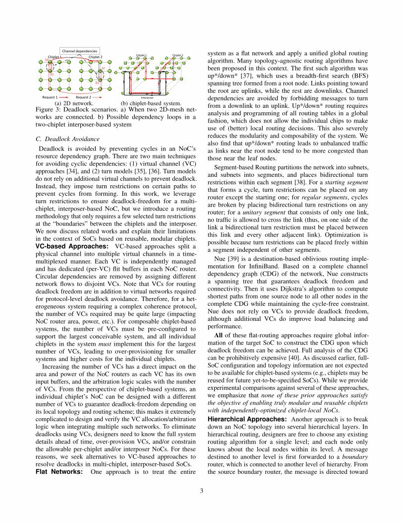
Chiplet 1 Chiplet 2
Channel dependencies
Request 1 Request 2
S1
D2
S2
D1
(a) 2D network.
Chiplet 1 Chiplet 2
Interposer
(b) chiplet-based system.Figure 3: Deadlock scenarios. a) When two 2D-mesh net-
works are connected. b) Possible dependency loops in a
two-chiplet interposer-based system
C. Deadlock Avoidance
Deadlock is avoided by preventing cycles in an NoC’s
resource dependency graph. There are two main techniques
for avoiding cyclic dependencies: (1) virtual channel (VC)
approaches [34], and (2) turn models [35], [36]. Turn models
do not rely on additional virtual channels to prevent deadlock.
Instead, they impose turn restrictions on certain paths to
prevent cycles from forming. In this work, we leverage
turn restrictions to ensure deadlock-freedom for a multi-
chiplet, interposer-based NoC, but we introduce a routing
methodology that only requires a few selected turn restrictions
at the “boundaries” between the chiplets and the interposer.
We now discuss related works and explain their limitations
in the context of SoCs based on reusable, modular chiplets.
VC-based Approaches: VC-based approaches split a
physical channel into multiple virtual channels in a time-
multiplexed manner. Each VC is independently managed
and has dedicated (per-VC) flit buffers in each NoC router.
Circular dependencies are removed by assigning different
network flows to disjoint VCs. Note that VCs for routing
deadlock freedom are in addition to virtual networks required
for protocol-level deadlock avoidance. Therefore, for a het-
erogeneous system requiring a complex coherence protocol,
the number of VCs required may be quite large (impacting
NoC router area, power, etc.). For composable chiplet-based
systems, the number of VCs must be pre-configured to
support the largest conceivable system, and all individual
chiplets in the system must implement this for the largest
number of VCs, leading to over-provisioning for smaller
systems and higher costs for the individual chiplets.
Increasing the number of VCs has a direct impact on the
area and power of the NoC routers as each VC has its own
input buffers, and the arbitration logic scales with the number
of VCs. From the perspective of chiplet-based systems, an
individual chiplet’s NoC can be designed with a different
number of VCs to guarantee deadlock-freedom depending on
its local topology and routing scheme; this makes it extremely
complicated to design and verify the VC allocation/arbitration
logic when integrating multiple such networks. To eliminate
deadlocks using VCs, designers need to know the full system
details ahead of time, over-provision VCs, and/or constrain
the allowable per-chiplet and/or interposer NoCs. For these
reasons, we seek alternatives to VC-based approaches to
resolve deadlocks in multi-chiplet, interposer-based SoCs.
Flat Networks: One approach is to treat the entire
system as a flat network and apply a unified global routing
algorithm. Many topology-agnostic routing algorithms have
been proposed in this context. The first such algorithm was
up*/down* [37], which uses a breadth-first search (BFS)
spanning tree formed from a root node. Links pointing toward
the root are uplinks, while the rest are downlinks. Channel
dependencies are avoided by forbidding messages to turn
from a downlink to an uplink. Up*/down* routing requires
analysis and programming of all routing tables in a global
fashion, which does not allow the individual chips to make
use of (better) local routing decisions. This also severely
reduces the modularity and composability of the system. We
also find that up*/down* routing leads to unbalanced traffic
as links near the root node tend to be more congested than
those near the leaf nodes.
Segment-based Routing partitions the network into subnets,
and subnets into segments, and places bidirectional turn
restrictions within each segment [38]. For a starting segment
that forms a cycle, turn restrictions can be placed on any
router except the starting one; for regular segments, cycles
are broken by placing bidirectional turn restrictions on any
router; for a unitary segment that consists of only one link,
no traffic is allowed to cross the link (thus, on one side of the
link a bidirectional turn restriction must be placed between
this link and every other adjacent link). Optimization is
possible because turn restrictions can be placed freely within
a segment independent of other segments.
Nue [39] is a destination-based oblivious routing imple-
mentation for InfiniBand. Based on a complete channel
dependency graph (CDG) of the network, Nue constructs
a spanning tree that guarantees deadlock freedom and
connectivity. Then it uses Dijkstra’s algorithm to compute
shortest paths from one source node to all other nodes in the
complete CDG while maintaining the cycle-free constraint.
Nue does not rely on VCs to provide deadlock freedom,
although additional VCs do improve load balancing and
performance.
All of these flat-routing approaches require global infor-
mation of the target SoC to construct the CDG upon which
deadlock freedom can be achieved. Full analysis of the CDG
can be prohibitively expensive [40]. As discussed earlier, full-
SoC configuration and topology information are not expected
to be available for chiplet-based systems (e.g., chiplets may be
reused for future yet-to-be-specified SoCs). While we provide
experimental comparisons against several of these approaches,
we emphasize that none of these prior approaches satisfy
the objective of enabling truly modular and reusable chiplets
with independently-optimized chiplet-local NoCs.
Hierarchical Approaches: Another approach is to break
down an NoC topology into several hierarchical layers. In
hierarchical routing, designers are free to choose any existing
routing algorithm for a single level; and each node only
knows about the local nodes within its level. A message
destined to another level is first forwarded to a boundary
router, which is connected to another level of hierarchy. From
the source boundary router, the message is directed toward
3
its destination through other boundary routers. An advantage
of hierarchical routing is that each level of the local network
is analyzed independently, and a locally-optimal routing
algorithm can be applied. However, as we discussed earlier,
when combining individual networks together, the global
network could still have deadlocks. As a result, care must
be taken to avoid global deadlocks, which usually results in
case-by-case analysis of all possible global routing paths [41],
[42]. Previous works proposed hierarchical NoCs based on
regular topologies such as bus, ring, mesh, and tree [42]–[44].
However, chiplets from different manufacturers might not be
designed with regular NoCs, and the integrated SoC system
might not be symmetric. Consequently, system-level deadlock
avoidance can still require great effort and is error-prone.
D. Comparison of Modularity
While there may be many possible definitions of “modularity,”
we focus on the key attributes listed in Table I.
Independently Designed Chiplets: Architects of an
individual chiplet should be able to design and optimize their
local NoC with little knowledge of the rest of the overall
SoC(s). VC-based approaches require the chiplet architect
to either have information for the overall SoC organization
(chiplet design no longer independent) or to over-provision
the number of VCs to support all possible SoCs in which
the chiplet may be used. Flat and hierarchical NoCs also
typically require full SoC information to analyze and ensure
deadlock freedom.
Enables Local Optimization: A modular design ap-
proach should allow a chiplet architect to locally optimize a
chiplet’s NoC independent of the final SoC organization. Flat
approaches require global SoC information, and therefore
intra-chiplet optimizations impacting the local topology,
routing algorithms, load balancing, etc., cannot be performed
in isolation. Hierarchical NoCs do enable some degree
of local chiplet-level optimization, although this still may
be constrained by the global analysis of the full CDG to
eliminate deadlocks. VC-based approaches as well as the
Composable scheme proposed in this paper effectively allow
arbitrary chiplet-level NoC organizations and optimizations.
Global CDG Not Required: Flat and Hierarchical NoCs
are not modular because constructing the dependency graph
requires all channels’ connectivity, and route assignment
cannot be performed until all chiplet networks are finalized.
It is also extremely difficult to optimize the local NoC without
impacting global routing decisions, as modifying the local
network changes the global CDG. VC-based approaches
offer more flexibility in local optimization and do not require
the global CDG; they require some global information in
order to assign VCs. Our Composable approach requires
some limited information about a chiplet to be shared with
the SoC integrator (but far less than the full set of channel
dependencies), and no dependency information to be shared
between independent chiplet designs.
Future-proof Chiplets: A chiplet could get integrated
in a future SoC that has yet to be designed. As the Flat
and Hierarchical NoC approaches require the global CDG,
Table I: Comparison of deadlock avoidance approaches.IndependentlyDesignedChiplets
EnablesLocal Op-timization
GlobalCDG NotRequired
Future-proofChiplets
HWCost
VC-based - ++ + - High
Flat NoCs -- - - -- Low
Hierarchical - + - -- Low
Composable(this work)
+ ++ ++ ++ Low
chiplets would be difficult to reuse as local NoC designs and
optimizations may already be fixed. VC-based approaches are
perhaps better off, but over-provisioning of VCs for yet-to-
be-considered SoCs may be expensive. Our Composable
methodology late-binds NoC decisions related to traffic
to/from the interposer to SoC design time (as opposed to
when designing the chiplet), thereby requiring the least effort
and rework to deploy the chiplet in new SoC organizations.
Hardware Cost: Apart from VC-based designs, the other
approaches modify the routing tables of the different NoC
components and so the hardware overhead is minimal. For
the VC-based approach, especially if over-provisioning for
future systems is required, the area impact of supporting a
larger number of VCs can become relatively costly.
IV. MULTI-CHIPLET ROUTING
In this section, we present our composable, topology-
agnostic, deadlock-free routing methodology for chiplet-
based systems. The key insight is simple-but-powerful: from
the perspective of any individual chiplet, the rest of the
system (independent of the total number of other chiplets or
interposer complexity) can all be abstracted away into a single
virtual node, which enables tractable analysis, optimization,
and correctness at a chiplet granularity. We detail one concrete
approach for chiplet-based routing, but this is one possible
solution that our key insight enables.
A. Overview
Before describing our methodology, we define some terms.
Definition 1 A boundary router of a chiplet connects the
chiplet to the interposer through a boundary link. Traffic
traversing from the interposer to the chiplet is called inbound
traffic; traffic from the chiplet to the interposer is called
outbound traffic.
Definition 2 The inbound reachability of a boundary
router b, InR(b), is the fraction of on-chiplet routers
that can be reached from the interposer through router b;0 < InR(b) ≤ 1.
Definition 3 The outbound reachability of a boundary router
b, OutR(b), is the fraction of on-chiplet routers that can
reach the interposer through router b; 0 < OutR(b) ≤ 1.
Definition 4 The inbound distance of a chiplet router
r, InD(r), is the topological distance from the nearest
boundary router that can reach r to router r.
Definition 5 The outbound distance of a chiplet router r,
OutD(r), is the topological distance from r to its nearest
reachable boundary router.
The goal of the composable routing methodology is to
isolate the design of individual chiplets and the interposer
4
as much as possible, allowing independent load balancing
optimizations on each chiplet and the interposer, while
still providing deadlock-free routing for the entire system.
In particular, we place unidirectional turn restrictions at
boundary routers on each chiplet. When applying turn
restrictions, the rest of the system is abstracted away with a
single node that is connected to all boundary routers. Turn
restrictions determine the inbound and outbound reachability
of each boundary router and guarantee that cyclic channel
dependencies do not exist within each chiplet. Then, the
reachability information is propagated to the interposer, which
is responsible for routing a message from one boundary
router to another. With the knowledge of the boundary
routers’ reachabilities, messages are forwarded to the correct
destination chiplet. Once a message reaches a destination
boundary router, the local chiplet NoC will route the message
to its final destination. This hierarchical approach uses two
sets of routing tables for each chiplet. The first set of tables is
used for routing messages locally within the same chiplet (this
is the conventional intra-chiplet routing), while the second
set steers outbound messages to the appropriate boundary
routers. More implementation details are provided at the
end of this section. Routing decisions corresponding to the
first routing table (intra-chiplet) can be made completely
independently from the rest of the system, which might not
even yet be defined.
B. Chiplet Design Guidelines
When designing the chiplet-level NoC, the number and
placement of boundary routers are two critical design
parameters that can impact the overall system performance.
These relate to the number of vertical (micro-bump) links
between the chiplet and the interposer.
Number of Boundary Routers: The number of boundary
routers determines the throughput a chiplet can sustain
for sending/receiving off-chip traffic; the more boundary
routers, the higher the off-chip traffic bandwidth. An extreme
case would be to connect each router on the chiplet to the
interposer with a vertical link, making every router a boundary
router, as previously considered by others [2], [22]. However,
such a design is likely to be over-provisioned for the expected
amount of off-chip traffic and could be constrained by the
available micro-bump density.
In determining the number of boundary routers per chiplet,
a key observation is that while the maximum number of
boundary routers possible is a function of the chiplet area,
the maximum useful bandwidth is a function of its perimeter.
For a chiplet with an n-by-n mesh, we have analytically
determined that with the interposer topologies considered in
this paper, n boundary routers are sufficient (the full analysis
is omitted for brevity). For the 4×4 chiplets assumed in
most of our experiments, we use four boundary routers per
chiplet. While we focus on meshes, our methodology applies
to other topologies (see Section VI).
Turn Restrictions at Boundary Routers: The simple
example from Fig. 3 shows that there can be numerous
potential dependency loops through the interposer, other
chiplets, etc., leading to an explosion in the number of
possible paths to be analyzed. To enable individual chiplet-
level routing decisions and make the inter-chip dependency
analysis tractable, we abstract away the rest of the system as a
single node and connect all boundary routers with the abstract
node (Fig. 4). Unlike prior works, this novel abstraction step
is the key to enabling the independent design of chiplets
without requiring global CDG information.
We use turn restrictions to break cycles containing the
abstract node and a pair of boundary routers. The abstract
node represents the rest of the system that designers of
individual chiplets do not need to have knowledge of, hence
turn restrictions do not apply to the abstract node. When
choosing prohibited turns for boundary routers, connectivity
must be preserved (i.e., a path must exist from each chiplet
router to the abstract node, and vice versa), so turn restrictions
that cause a disconnected NoC are prohibited.
Breaking all cycles while maintaining connectivity is
sufficient to ensure the correctness of operation with respect
to this chiplet. However while sufficient, careful selection of
turn restrictions and routing are still desired for performance
reasons. Different heuristics can be employed; we describe
one possible approach that works well in practice. We
consider inbound and outbound reachability for load bal-
ancing. An imbalanced inbound or outbound reachability can
cause the chiplet and/or the interposer to become congested.
Meanwhile, the average of inbound and outbound distances
across all chiplet routers should be minimized, due to the
fact that when routing off-chip, the nearest boundary router
is preferred if a message has multiple boundary router candi-
dates. Overall when choosing prohibited turns, our objective
is to minimize Average distanceAverage reachability
, in which distance and
reachability are defined in Section IV-A, and the averages
are computed across all on-chip routers. To be specific,
Average distance is the average of inbound and outbound
distance for all routers on the chiplet. Average reachabilityis similarly computed over each boundary router’s inbound
and outbound reachability. Our heuristic selects combinations
with lower average distances and higher average reachability.
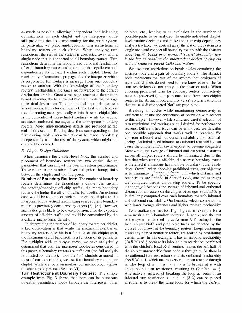
To visualize the metrics, Fig. 4 gives an example for a
4×4 mesh with 3 boundary routers a, b, and c; and the rest
of the system is denoted by x. Assume X-Y routing for the
local chiplet NoC, and prohibited turns are denoted by the
crossed-out arrows at the boundary routers. Loops containing
x and any pair of boundary routers are broken by prohibiting
certain turns. In this example, a has an inbound reachability
(InR(a)) of 12 because its inbound turn restriction, combined
with the chiplet’s local X-Y routing, makes the left half of
the chiplet unreachable from node x through a. As there is
no outbound turn restriction on a, its outbound reachability
OutR(a) is 1, which means every router can reach x through
a. The loop of x → a → c → x is broken at c with
an outbound turn restriction, resulting in OutR(c) = 12 .
Alternatively, instead of breaking the loop at router c, an
inbound turn restriction x → a → (3, 3) can be placed
at router a to break the same loop, for which the InR(a)
5
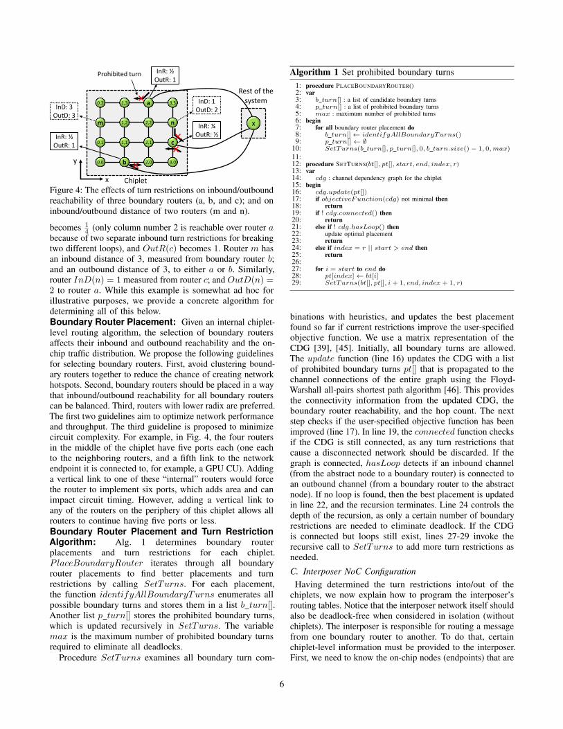
0,3 1,3 a 3,3
m 1,2 2,2 n
0,1 1,1 2,1 c
0,0 b 2,0 3,0
Rest of the
system
Chiplet
Prohibited turn
x
y
InD: 3
OutD: 3
InR: ½
OutR: 1
InR: ½
OutR: 1
x
InD: 1
OutD: 2
InR: ¼
OutR: ½
Figure 4: The effects of turn restrictions on inbound/outbound
reachability of three boundary routers (a, b, and c); and on
inbound/outbound distance of two routers (m and n).
becomes 14 (only column number 2 is reachable over router a
because of two separate inbound turn restrictions for breaking
two different loops), and OutR(c) becomes 1. Router m has
an inbound distance of 3, measured from boundary router b;and an outbound distance of 3, to either a or b. Similarly,
router InD(n) = 1 measured from router c; and OutD(n) =2 to router a. While this example is somewhat ad hoc for
illustrative purposes, we provide a concrete algorithm for
determining all of this below.
Boundary Router Placement: Given an internal chiplet-
level routing algorithm, the selection of boundary routers
affects their inbound and outbound reachability and the on-
chip traffic distribution. We propose the following guidelines
for selecting boundary routers. First, avoid clustering bound-
ary routers together to reduce the chance of creating network
hotspots. Second, boundary routers should be placed in a way
that inbound/outbound reachability for all boundary routers
can be balanced. Third, routers with lower radix are preferred.
The first two guidelines aim to optimize network performance
and throughput. The third guideline is proposed to minimize
circuit complexity. For example, in Fig. 4, the four routers
in the middle of the chiplet have five ports each (one each
to the neighboring routers, and a fifth link to the network
endpoint it is connected to, for example, a GPU CU). Adding
a vertical link to one of these “internal” routers would force
the router to implement six ports, which adds area and can
impact circuit timing. However, adding a vertical link to
any of the routers on the periphery of this chiplet allows all
routers to continue having five ports or less.
Boundary Router Placement and Turn RestrictionAlgorithm: Alg. 1 determines boundary router
placements and turn restrictions for each chiplet.
PlaceBoundaryRouter iterates through all boundary
router placements to find better placements and turn
restrictions by calling SetTurns. For each placement,
the function identifyAllBoundaryTurns enumerates all
possible boundary turns and stores them in a list b turn[].Another list p turn[] stores the prohibited boundary turns,
which is updated recursively in SetTurns. The variable
max is the maximum number of prohibited boundary turns
required to eliminate all deadlocks.
Procedure SetTurns examines all boundary turn com-
Algorithm 1 Set prohibited boundary turns
1: procedure PLACEBOUNDARYROUTER()2: var3: b turn[] : a list of candidate boundary turns4: p turn[] : a list of prohibited boundary turns5: max : maximum number of prohibited turns6: begin7: for all boundary router placement do8: b turn[]← identifyAllBoundaryTurns()9: p turn[]← ∅
10: SetTurns(b turn[], p turn[], 0, b turn.size()− 1, 0,max)
11:12: procedure SETTURNS(bt[], pt[], start, end, index, r)13: var14: cdg : channel dependency graph for the chiplet15: begin16: cdg.update(pt[])17: if objectiveFunction(cdg) not minimal then18: return19: if ! cdg.connected() then20: return21: else if ! cdg.hasLoop() then22: update optimal placement23: return24: else if index = r || start > end then25: return26:27: for i = start to end do28: pt[index]← bt[i]29: SetTurns(bt[], pt[], i + 1, end, index + 1, r)
binations with heuristics, and updates the best placement
found so far if current restrictions improve the user-specified
objective function. We use a matrix representation of the
CDG [39], [45]. Initially, all boundary turns are allowed.
The update function (line 16) updates the CDG with a list
of prohibited boundary turns pt[] that is propagated to the
channel connections of the entire graph using the Floyd-
Warshall all-pairs shortest path algorithm [46]. This provides
the connectivity information from the updated CDG, the
boundary router reachability, and the hop count. The next
step checks if the user-specified objective function has been
improved (line 17). In line 19, the connected function checks
if the CDG is still connected, as any turn restrictions that
cause a disconnected network should be discarded. If the
graph is connected, hasLoop detects if an inbound channel
(from the abstract node to a boundary router) is connected to
an outbound channel (from a boundary router to the abstract
node). If no loop is found, then the best placement is updated
in line 22, and the recursion terminates. Line 24 controls the
depth of the recursion, as only a certain number of boundary
restrictions are needed to eliminate deadlock. If the CDG
is connected but loops still exist, lines 27-29 invoke the
recursive call to SetTurns to add more turn restrictions as
needed.
C. Interposer NoC Configuration
Having determined the turn restrictions into/out of the
chiplets, we now explain how to program the interposer’s
routing tables. Notice that the interposer network itself should
also be deadlock-free when considered in isolation (without
chiplets). The interposer is responsible for routing a message
from one boundary router to another. To do that, certain
chiplet-level information must be provided to the interposer.
First, we need to know the on-chip nodes (endpoints) that are
6
reachable from each individual boundary router given the turn
restrictions. We use this to ensure that a message is routed
to a chiplet’s boundary router from which the destination
can be reached. Second, we optionally use the topological
distances between each boundary router and its reachable on-
chip nodes to optimize routing distances and load balancing.
Note that this information can simply be enumerated in a
“list” format (e.g., node x is reachable from boundary node
y); the full details of the chiplet’s local NoC are not required
(e.g., the topology of the network and routing decisions for
how a request gets from y to x) and this information is
independent of the interposer and any other chiplets.We now describe our interposer routing scheme. For each
message destined to a router on a chiplet, the following algo-
rithm decides which boundary router of the destination chiplet
to send this message to. If a destination is only reachable
through a single boundary router, then the interposer must
route the message to that specific boundary router. Otherwise,
we pick boundary routers to balance network load across
the boundary routers (equally utilizing chiplet-interposer
bandwidth) while minimizing path lengths (avoid sending
messages on highly-circuitous just for load balancing). Below,
we formally specify the algorithm.• For a given boundary router i, the set of nodes that are
reachable ONLY by i is denoted as Ai.
• For the remaining nodes that can be reached by more
than one boundary router, the list Ci contains all nodes
that are topologically closer to i than any other boundary
routers. For different boundary routers j and k, Cj ∩Ck = ∅.
• The remaining nodes are equidistant to at least two
boundary routers. Let Ei,j be the list of nodes that are
equidistant to both boundary routers i and j. While
being equidistant to more than two boundary routers
is possible, we only consider the two-router case for
simplicity.
• Perform the following steps to assign on-chip nodes to
boundary routers.
Step 1. Across all boundary routers, select a router ithat has the minimum number of items in Ai.
Step 2. Assign nodes from Ci to Ai one by one, until
the number of items in Ai is not the smallest. An item
is removed from Ci when assigned to Ai. If Ai still
has the minimum number of items, assign node from
Ei,j to Ai one by one. Items are removed from Ei,j
and Ej,i after assignment to Ai.
Step 3. Node assignment to boundary router i is finished
if no further assignment can be made. Repeat Steps 1-3,
until Ci = ∅ and Ei,j = ∅ for all boundary routers iand j.
When finished, the node assignment information for each
boundary router is stored in Ai. By referring to this informa-
tion, the interposer routing table is configured accordingly.
The system integrator is free to choose any underlying routing
algorithm that is deadlock-free for the interposer network.Consider the example shown in Fig. 4. For boundary
routers a, b, and c, Aa = {(2, 0), (2, 1), (2, 2), a}, Ab =
{(0, 0), (0, 1),m, (0, 3), b, (1, 1), (1, 2), (1, 3)}, and Ac = ∅;
and Ca = {(3, 3)}, Cb = ∅, Cc = {(3, 0), c, n}. There is no
equidistant set in this network. Node assignment starts with
boundary router c because Ac is empty. All the elements in
Cc are assigned to Ac and Ac = {(3, 0), c, n}. No further
assignment can be performed for c, therefore the algorithm
chooses the next router, which is a. The only element in Ca
is assigned to Aa and Aa = {(2, 0), (2, 1), (2, 2), a, (3, 3)}.
Up to this point, each on-chip node is assigned to exactly
one boundary router; and the assignments are stored in Aa,
Ab, and Ac. With the above information, the interposer is
able to route a message to the correct boundary router (a, b,or c) if the message is destined to this chiplet.
D. Deadlock Freedom and Connectivity
Now we show that the composable routing scheme is
deadlock free and connected. Assume that there is a cycle
r1, l1, r2, l2, ..., rn, ln, in which r denotes a router and l is a
link connected to r. If all of the routers and links belong to the
same chiplet, then it contradicts the basic assumption that the
chiplet-level network is deadlock free. Otherwise, if a subset
of the cycle belongs to the interposer and other chiplets, this
subset can be abstracted with a single node x. Therefore,
the cycle is converted into r1, l1, ..., rj , x, rk, lk, ..., rn, ln.
Because all cyclic dependencies in loops containing x are
removed, the new cycle is deadlock free. As a result, the
composable routing scheme is deadlock free.Any network within a single chiplet is connected, because
boundary router turn restrictions do not affect the internal
chiplet network. Any node on a chiplet is able to reach
the interposer through at least one boundary router. The
interposer network is connected by construction (i.e., every
interposer router can reach every other interposer router).
Given any pair of on-chip nodes, a path exists between the
two nodes. As a result, the system is connected.
E. Microarchitectural Issues
Each chiplet needs to implement two different routing
tables. The first handles intra-chiplet traffic that never goes
to the interposer. This routing table may be populated in
whatever manner the chiplet designer deems appropriate.
The second routing table directs outbound traffic to the
appropriate boundary router. This organization assumes a
global ID space for all of the router endpoints throughout the
collective system. Analogous to the boot-up sequences used
to detect all of the memory and compute resources available
in a system (especially in a multi-socket SMP system),
composable interposer-based SoCs would need a similar
protocol for system configuration. Part of this process would
be the detection of the available NoC endpoints, assignment
of unique IDs to each endpoint, and the computation and
population of the secondary routing tables. Unlike system
boot-up, this process would only be performed once by the
SoC integrator after physically assembling the SoC (although
hooks may also be provided to update the tables at a later
point in time, such as to handle failed links [32]).In our design, each network interface (NI) has a lookup
table that maps the destination ID of an outbound packet to a
7
boundary router ID. The boundary router ID is then embedded
in the header flit and used for intra-chiplet routing until the
packet leaves the chiplet. Regarding area/power overhead, the
lookup table in each NI needs to provision against the largest
system size for a given generation of products. Routing tables
are typically much smaller than other router components
such as buffers and crossbars. Furthermore, the size of the
second routing table in each chiplet is only proportional
to the number of boundary routers; thus, it is significantly
smaller than the first routing table. There are several ways to
implement the interposer router: 1) Provision the routing
tables for the largest system size, resulting in relatively
large interposer routing tables; or 2) Add another layer of
destination mapping to convert destination IDs to destination
boundary router IDs, leading to smaller routing tables but
more complex boundary routers. Overall, our design should
not incur significant additional power/area/timing impact
compared to a canonical two-stage router.
V. EVALUATION
A. Experimental Methodology
To evaluate network performance, we use an APU simulation
platform consisting of gem5 [47] and a modified version
of the GPU model [48] for cycle-level execution-driven
simulations. We use Garnet [49] to simulate the network
using 2-stage routers with 4-flit buffers per channel. Our
initial experiments use the multi-chiplet APU configuration
shown in Fig. 2 consisting of four GPU chiplets, one CPU
chiplet, and an active interposer. The CPU chiplet consists of
CPU cores, private CPU L1 and L2 caches, and a last level
cache. Each GPU chiplet consists of 16 compute units (CUs)
and 8 GPU L2 cache banks. Our memory model utilizes the
built-in gem5 model [50] with eight memory channels and
eight banks per channel. Fig. 2 also shows the placement of
the boundary nodes as determined by our algorithm from
Section IV.
We use both synthetic traffic and application-based simu-
lation. For synthetic traffic, each packet is 8 flits wide, and
the network is simulated for 2 million cycles. For system-
level (non-synthetic) simulations, we use APU applications
from the AMD SDK [51], Rodinia [52], and Pannotia [53]
suites, where off-chiplet communication includes both cache
coherence between GPU CUs and traffic to main memory.
B. Comparison Points
Even though qualitatively the VC-based approach is ex-
pensive and unattractive, we provide a comparison for
completeness. Using a similar methodology as EbDa [40],
we implement a VC-based deadlock avoidance mechanism
that supports minimal-path adaptive routing using four VCs:
two VCs are needed to avoid deadlock for a single 2D mesh;
by introducing vertical connections between chiplet and the
interposer, two more VCs are required to isolate inbound and
outbound traffic. We also implement three global routing
algorithms described in Section III-C: up*/down* [37],
segment-based [38], and Nue routing [39]. Note that all three
require full CDG knowledge and do not enable independent
0
50
100
150
200
0.0005 0.0045 0.0085 0.0125 0.0165
Av
era
ge
La
ten
cy
Injection rate (packets/cycle/node)
shortest path updown
segbased VC-based
Nue composable
(a) Uniform random.
0
50
100
150
200
0.0005 0.0045 0.0085 0.0125 0.0165
Av
era
ge
La
ten
cy
Injection rate (packets/cycle/node)
shortest path updown
segbased VC-based
Nue composable
(b) Bit complement.Figure 5: Load-latency curve w/ synthetic traffic.
3.94
0
0.5
1
1.5
2
2.5
No
rma
lize
d L
ate
ncy
shortest path composable up*/down*
(a) Network latency.
1.44
0.8
0.9
1
1.1
1.2
No
rma
lize
d R
un
tim
e
shortest path composable up*/down*
(b) Execution time.Figure 6: System performance under realistic traffic.
design and chiplet reuse. We compare against them as the
most relevant work that we are aware of, but they fail to
satisfy our key chiplet modularity criteria.
The root node in up*/down* routing is selected by finding
the node with the lowest average distance to all other nodes
before applying turn restrictions. The starting segment in
segment-based routing is formed from the top-left of the
system (the top-left router of the top-left GPU chiplet). In our
composable routing scheme, both the local chiplet algorithms
and the interposer algorithm use dimension-ordered routing.
For fair comparison against the VC-based approach, we
provide four VCs for each of the turn-based schemes.
We also compare our results to an idealized system
(denoted as shortest path) that uses an impractically large
number of virtual channels to avoid deadlock. The routing
tables are configured using an all-pairs shortest path (APSP)
algorithm (in contrast to the prior-art and our own proposed
scheme where some routes may not be minimal). Note
that this idealized system does not necessarily provide
true optimal performance because APSP can still lead to
higher levels of congestion in some links compared to
others. However in practice, we find that this shortest-path
configuration typically outperforms the practical alternatives,
and so it provides an optimistic performance target to
compare against.
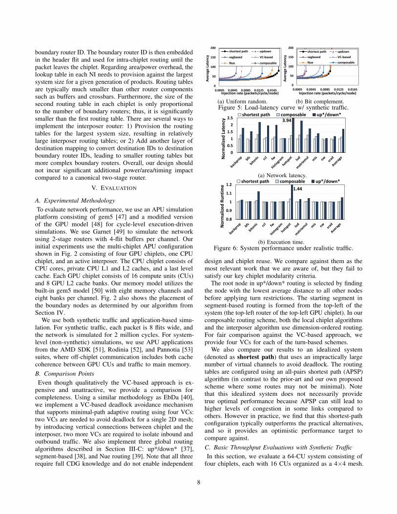
C. Basic Throughput Evaluations with Synthetic Traffic
In this section, we evaluate a 64-CU system consisting of
four chiplets, each with 16 CUs organized as a 4×4 mesh.
8
Each chiplet is connected to the interposer through four
boundary routers. The interposer network is a 4×4 mesh.
Fig. 5a and Fig. 5b show the load-latency curves under
uniform random and bit complement traffic. We observed that
many heterogeneous multi-chiplet workloads have similarities
to uniform random traffic: the real system has a mix of
intra-chiplet, inter-chiplet, chiplet-to-interposer, and chiplet-
to-memory traffic covering both coherence and main memory
requests and responses; these in aggregate “average out” such
that the high-level performance trends of uniform random
traffic largely match several of our application-driven studies.
The bit complement traffic pattern forces all packets to go off-
chiplet, therefore it further stresses the interposer and creates
network hotspots. We ran other synthetic traffic patterns, but
the overall trends were very similar so they were not shown.
Our composable scheme outperforms up*/down*, segment-
based, and VC-based approaches.1 With the same number
of VCs, the composable scheme performs better than the
VC-based approach mainly because the extra VCs reduce
head-of-line blocking. Typical coherence protocols require
between 3-5 virtual networks, each of which would require
four VCs for deadlock freedom in the VC-based approach.
A coherence protocol for a heterogeneous architecture may
well require more virtual networks making the VC-based
approach even more expensive. While the VC-based approach
requires four VCs/virtual network for correctness, more VCs
are needed for performance as indicated by the performance
gap between the VC-based and composable schemes.
Segment-based routing suffers from larger zero-load la-
tency and has the lowest saturation throughput. This is
mainly because it is designed and optimized for 2D mesh-
like networks. Although the evaluated system consists of
multiple mesh networks, the global topology remains irregular
such that segment-based routing cannot efficiently handle it.
The baseline segment-based algorithm does not always form
an optimal segment; a segment starting from a boundary
router toward the interposer is likely to wrap around and end
on a router on the same chiplet, or traverse multiple hops
through another chiplet until it reaches a router belonging
to an existing segment. Such chain-like segments can be
very long in larger systems, and breaking any bidirectional
turns within the segment will result in more non-minimal
paths (for the baseline APU, we observed an average routing
distance of nearly 11 hops, as opposed to ∼8 hops for the
other approaches). Although topology-aware optimization
might improve the performance of segment-based routing, it
is out of the scope of this paper.
Up*/down* routing has low zero-load latency, which
indicates that messages are likely to take minimal routes
in the evaluated system. However, it saturates relatively
early compared to the other approaches. Links near the
root node are inherently more congested than those near
the leaf nodes. When injection rate increases, these links
1In the absence of network contention, head-of-line blocking, etc., the theoretical
saturation throughput for uniform random and bit complement traffic are 0.031 and
0.016 packets/cycle/node, respectively.
saturate and become bottlenecks. Nue routing outperforms
our composable approach, but does so only because it has the
benefit of optimizing its routing with knowledge of the full
CDG, resulting in similar behavior to the ideal shortest-path
algorithm. With sufficient VCs (which we provision it with),
it finds optimized paths to balance the network workload.
Our composable scheme outperforms up*/down* and
segment-based routing because the chiplet and interposer
networks are more load balanced, as are the vertical links
between the chiplets and the interposer. Nue provides better
load balancing and therefore performs close to idealized
shortest-path routing, but like the other prior works it is
not applicable for independent design and reuse of chiplets
for modular SoC construction. Compared to the idealized
shortest-path routing, our scheme covers much of the through-
put gap from up*/down*, but there remains some headroom.
This is because of 1) some remaining load imbalance due to
turn restrictions, and 2) the idealized network has more virtual
channels to improve head-of-line blocking. Overall, although
our proposed approach does not achieve the full performance
of globally-load balanced optimization, our results show
that our scheme ensures correctness while delivering high
performance for multi-chiplet SoCs, and it uniquely enables
a modular chiplet-based design methodology that does not
require a priori knowledge of the full system’s CDG.
D. Application-level Impact
Network Latency: We evaluate our composable routing
scheme with non-synthetic workloads using execution-driven
simulation. Fig. 6a shows the average network latency,
normalized to the idealized shortest-path approach. Segment-
based routing is not shown because it is consistently and
significantly out-performed by the remaining approaches
at the given system size. We omit the VC-based scheme
because the evaluated heterogeneous system requires an
impractically large number of VCs to avoid routing and
protocol-level deadlock while retaining performance. Overall,
our composable approach achieves network latencies that are
nearly the same as the shortest-path case. There are a few
cases (bfs, nw, srad) where the composable routing performs
marginally better than shortest path; as discussed earlier,
shortest-path is not truly optimal, and there are occasionally
situations where localized bursts of traffic (which occurs more
often in GPU workloads than conventional CPU applications)
can cause congestion/load imbalance in the shortest-path
configuration.
The up*/down* approach suffers over 50% increases
in average network latency for most benchmarks because
the root node becomes the bottleneck under heavy traffic,
as discussed in Section V-C. Such bottlenecks limit the
system’s effective bandwidth and lead to significant in-
network buffering delays.
Application Performance: Fig. 6b shows the program
execution time, normalized to the idealized shortest path
approach. Overall, composable routing achieves similar
(within 1%) system performance compared to shortest path.
While APU/GPGPU applications generate large bursts of
9
InterposerGPU Chiplet 68%
74%72%
70%
75%
68%72%
75%
74%
70%
73%
68%
(a) Shortest path routing.
82% 82%
73%
76%
64%
79%
73%
65%
73%
74%
InterposerGPU Chiplet
(b) Composable routing.
70%
82% 87% 78%
79%
75%
63%
Root Node
InterposerGPU Chiplet
(c) Up*/down* routing.Figure 7: Maximum link utilization for HotSpot application.
NoC/memory traffic (which is great for stressing the network),
the overall impact on application execution time is muted
because most GPU applications are inherently less sensitive
to latency (i.e., increased latency can be more easily tolerated
by abundant SIMD parallelism). While there are bursts of
traffic, significant portions of the applications do not operate
the NoC near saturation, and so there is less impact on
total execution time. Nevertheless, we still observe a 5-10%
performance degradation with up*/down* routing for some
workloads while our approach performs at about the same
level as the shortest-path approach.
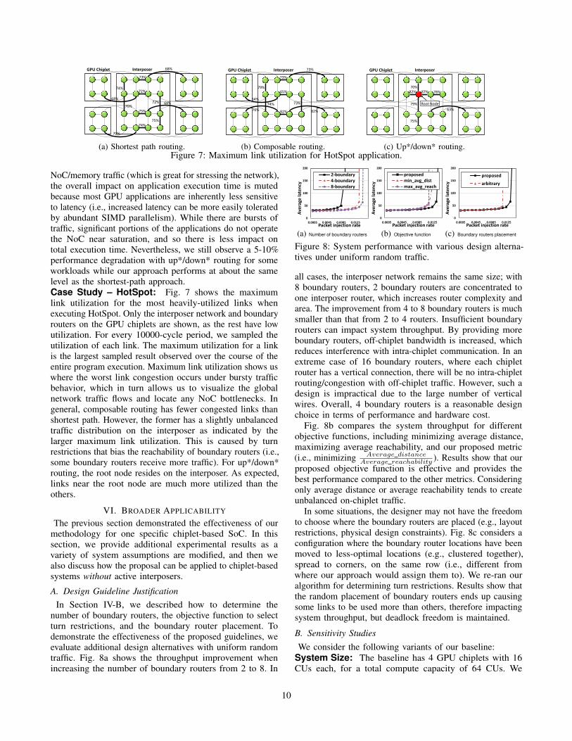
Case Study – HotSpot: Fig. 7 shows the maximum
link utilization for the most heavily-utilized links when
executing HotSpot. Only the interposer network and boundary
routers on the GPU chiplets are shown, as the rest have low
utilization. For every 10000-cycle period, we sampled the
utilization of each link. The maximum utilization for a link
is the largest sampled result observed over the course of the
entire program execution. Maximum link utilization shows us
where the worst link congestion occurs under bursty traffic
behavior, which in turn allows us to visualize the global
network traffic flows and locate any NoC bottlenecks. In
general, composable routing has fewer congested links than
shortest path. However, the former has a slightly unbalanced
traffic distribution on the interposer as indicated by the
larger maximum link utilization. This is caused by turn
restrictions that bias the reachability of boundary routers (i.e.,
some boundary routers receive more traffic). For up*/down*
routing, the root node resides on the interposer. As expected,
links near the root node are much more utilized than the
others.
VI. BROADER APPLICABILITY
The previous section demonstrated the effectiveness of our
methodology for one specific chiplet-based SoC. In this
section, we provide additional experimental results as a
variety of system assumptions are modified, and then we
also discuss how the proposal can be applied to chiplet-based
systems without active interposers.
A. Design Guideline Justification
In Section IV-B, we described how to determine the
number of boundary routers, the objective function to select
turn restrictions, and the boundary router placement. To
demonstrate the effectiveness of the proposed guidelines, we
evaluate additional design alternatives with uniform random
traffic. Fig. 8a shows the throughput improvement when
increasing the number of boundary routers from 2 to 8. In
0
50
100
150
200
0.0005 0.0045 0.0085 0.0125
Av
era
ge
la
ten
cy
Packet injection rate
2-boundary
4-boundary
8-boundary
(a) Number of boundary routers
0
50
100
150
200
0.0005 0.0045 0.0085 0.0125
Av
era
ge
la
ten
cy
Packet injection rate
proposed
min_avg_dist
max_avg_reach
(b) Objective function
0
50
100
150
200
0.0005 0.0045 0.0085 0.0125
Av
era
ge
la
ten
cy
Packet injection rate
proposed
arbitrary
(c) Boundary routers placement
Figure 8: System performance with various design alterna-
tives under uniform random traffic.
all cases, the interposer network remains the same size; with
8 boundary routers, 2 boundary routers are concentrated to
one interposer router, which increases router complexity and
area. The improvement from 4 to 8 boundary routers is much
smaller than that from 2 to 4 routers. Insufficient boundary
routers can impact system throughput. By providing more
boundary routers, off-chiplet bandwidth is increased, which
reduces interference with intra-chiplet communication. In an
extreme case of 16 boundary routers, where each chiplet
router has a vertical connection, there will be no intra-chiplet
routing/congestion with off-chiplet traffic. However, such a
design is impractical due to the large number of vertical
wires. Overall, 4 boundary routers is a reasonable design
choice in terms of performance and hardware cost.
Fig. 8b compares the system throughput for different
objective functions, including minimizing average distance,
maximizing average reachability, and our proposed metric
(i.e., minimizing Average distanceAverage reachability
). Results show that our
proposed objective function is effective and provides the
best performance compared to the other metrics. Considering
only average distance or average reachability tends to create
unbalanced on-chiplet traffic.
In some situations, the designer may not have the freedom
to choose where the boundary routers are placed (e.g., layout
restrictions, physical design constraints). Fig. 8c considers a
configuration where the boundary router locations have been
moved to less-optimal locations (e.g., clustered together),
spread to corners, on the same row (i.e., different from
where our approach would assign them to). We re-ran our
algorithm for determining turn restrictions. Results show that
the random placement of boundary routers ends up causing
some links to be used more than others, therefore impacting
system throughput, but deadlock freedom is maintained.
B. Sensitivity Studies
We consider the following variants of our baseline:
System Size: The baseline has 4 GPU chiplets with 16
CUs each, for a total compute capacity of 64 CUs. We
10
also consider two 128-CU configurations (CPU count held
constant) consisting of (1) 4 chiplets with 32 CUs each, and
(2) 8 chiplets with 16 CUs each. In both cases, there are still
four boundary routers per chiplet.
Interposer NoC Topology: To support the claim that
the interposer’s NoC can be designed independently from
the chiplets, we evaluate our baseline system but replace
the interposer’s mesh NoC with a “Double Butterfly” topol-
ogy [22].
Irregular Chiplet Topologies: To support the similar
claim that the chiplets’ NoC topologies can be independently
designed, we evaluate a system where each GPU chiplet
implements a different local NoC topology consisting of
mesh, ring, butterfly, and tree topologies.
Results: The analyses in this section are presented only
with the load-latency curves for uniform random traffic. We
did perform application-level experiments as well, but the
overall trends are very consistent, and so we omit those
additional graphs due to space reasons and their repetitiveness.
The main point of these experiments is to demonstrate that
our proposal is a robust way to achieve high performance
while ensuring deadlock freedom across a wide range of
chiplet-based system possibilities.
Fig. 9a and b show the results for the larger 128-CU
configurations, with our composable approach handily out-
performing up*/down* routing. The major difference between
these two configurations is the ratio of intra-chiplet to inter-
chiplet traffic. Compared to shortest path, our composable
approach is less sensitive to traffic distribution due to better
chiplet-level and interposer-level load balancing.
Fig. 9c shows the results when the interposer NoC has
a butterfly-based topology. The results are similar to the
baseline system with the mesh, and overall this helps to
demonstrate that the individual chiplets can be easily designed
independent of the interposer’s NoC topology.
Fig. 9d shows the results when each of the GPU chiplets
has a different local NoC topology. The results here are
more interesting as our proposal results in a higher saturation
throughput than the “ideal” case with copious virtual channels
and shortest path routing. This is because when handling
inter-chiplet communication, shortest path favors boundary
routers near the center of the interposer while our proposed
approach achieves better distribution of interposer traffic.
C. Other Chiplet Packaging Options
Thus far, our studies have focused on chiplet-based systems
built on emerging active silicon interposer technologies.
While active silicon interposers can be practical, especially
if the total amount of interposer area used for logic can
be minimized [2], [30], near-term chiplet systems may
be limited to passive substrates. Whether using a passive
silicon interposer [19]–[21] or a more conventional packaging
substrate [7], [11], [14], [54], one possible concern is that
the lack of an active layer below the chiplets could constrain
the applicability of our methodology.
Fig. 10a shows an example system with chiplets on a
passive substrate. This layout assumes a central chip that
0
50
100
150
200
0.0005 0.0085 0.0165
Av
era
ge
la
ten
cy
Packet injection rate
shortest path
updown
composable
(a) Four 32-CU chiplets
0
50
100
150
200
0.0005 0.0085 0.0165
Av
era
ge
la
ten
cy
Packet injection rate
shortest path
updown
composable
(b) Eight 16-CU chiplets
0
50
100
150
200
0.0005 0.0085 0.0165
Av
era
ge
la
ten
cy
Packet injection rate
shortest path
updown
composable
(c) Butterfly interposer
0
50
100
150
200
0.0005 0.0085 0.0165
Av
era
ge
la
ten
cy
Packet injection rate
shortest path
updown
composable
(d) Irregular chiplet NoCs
Figure 9: Load-latency curves for different system configu-
rations under uniform random traffic.
(a)
CPU
GPU
GPU GPU
GPU
Co
mm
on
Passive substrate
(b)
GPU
GPU GPU
GPU
Co
mm
on
Virtual chiplet
CP
U
CP
U
(c)
GPU
GPU GPU
GPU
Virtual central chip
CPU
Common
Common
Figure 10: Chiplet-based systems on passive substrates (e.g.,
passive interposer, MCM).
provides the common functionality that would otherwise be
put on the active interposer (e.g., memory controllers, NoC,
system management), with the compute chiplets fanning
out from the central chip in a star-like topology. With this
type of layout, our proposed methodology can be applied
directly to this system without any modification by treating
the central chip in the same way as the active interposer in
our previous working example. The process for selecting the
best boundary node placement can be more efficient as there
are fewer reasonable nodes on a chiplet to choose from (i.e.,
those closest to the central chip).
D. Other Chiplet Topologies
Even for chiplets in a non-star topology, our approach can be
adapted to work. Fig. 10b shows a chiplet-based system where
two CPU chiplets have additional point-to-point links (e.g.,
for low-latency cache coherence) that do not route through
the central chip. To support this, the two CPU chiplets are
effectively treated as a single virtual chiplet in order to
apply our methodology to determine routing restrictions. It
is still up to the CPU chiplet designer to ensure that the
routing directly between the two CPU chiplets is correct (i.e.,
deadlock free), but the designers need not worry about traffic
entering/leaving either of the chiplets from/to the central
chip as our methodology determines the appropriate turn
restrictions to ensure proper operation of the overall SoC.
Likewise, Fig. 10c shows a system where there is no
single “central” chip, but rather there are two chips that the
other chiplets connect to. Here, we apply a similar technique
where the two chips are treated as a single virtual chip
for the purposes of this approach. Similar to the two-CPU
chiplet example above, the SoC designer must ensure that
11
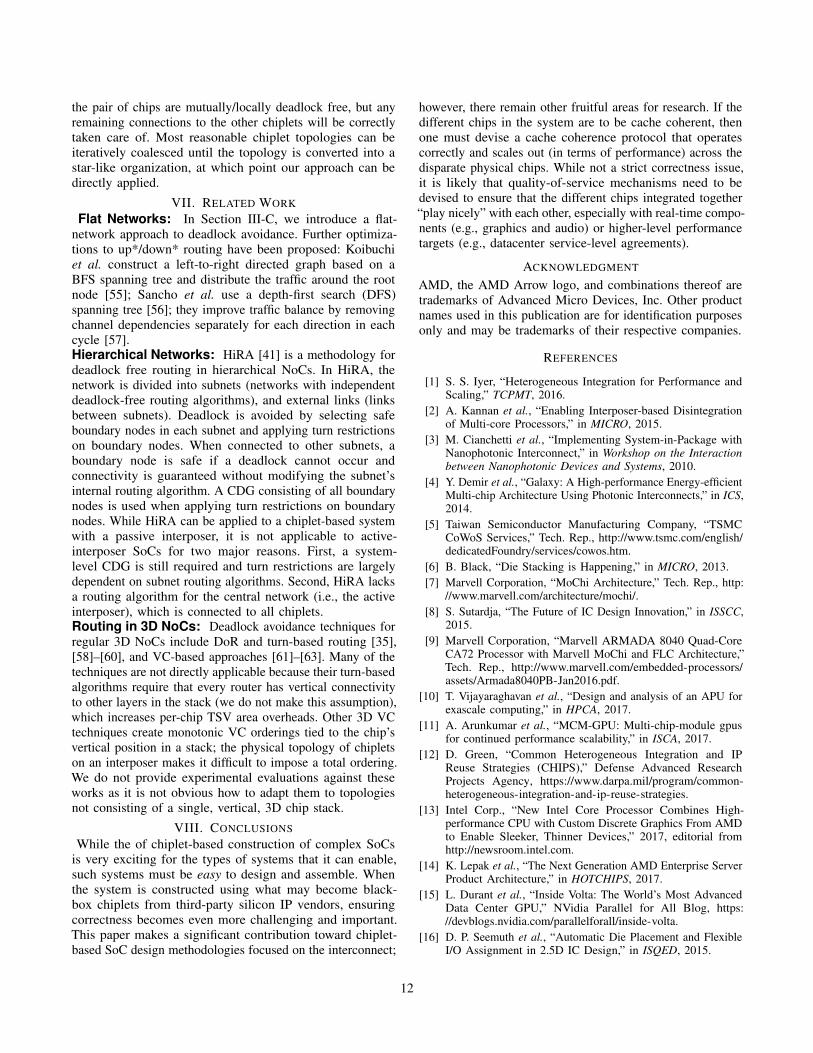
the pair of chips are mutually/locally deadlock free, but any
remaining connections to the other chiplets will be correctly
taken care of. Most reasonable chiplet topologies can be
iteratively coalesced until the topology is converted into a
star-like organization, at which point our approach can be
directly applied.
VII. RELATED WORK
Flat Networks: In Section III-C, we introduce a flat-
network approach to deadlock avoidance. Further optimiza-
tions to up*/down* routing have been proposed: Koibuchi
et al. construct a left-to-right directed graph based on a
BFS spanning tree and distribute the traffic around the root
node [55]; Sancho et al. use a depth-first search (DFS)
spanning tree [56]; they improve traffic balance by removing
channel dependencies separately for each direction in each
cycle [57].Hierarchical Networks: HiRA [41] is a methodology for
deadlock free routing in hierarchical NoCs. In HiRA, the
network is divided into subnets (networks with independent
deadlock-free routing algorithms), and external links (links
between subnets). Deadlock is avoided by selecting safe
boundary nodes in each subnet and applying turn restrictions
on boundary nodes. When connected to other subnets, a
boundary node is safe if a deadlock cannot occur and
connectivity is guaranteed without modifying the subnet’s
internal routing algorithm. A CDG consisting of all boundary
nodes is used when applying turn restrictions on boundary
nodes. While HiRA can be applied to a chiplet-based system
with a passive interposer, it is not applicable to active-
interposer SoCs for two major reasons. First, a system-
level CDG is still required and turn restrictions are largely
dependent on subnet routing algorithms. Second, HiRA lacks
a routing algorithm for the central network (i.e., the active
interposer), which is connected to all chiplets.Routing in 3D NoCs: Deadlock avoidance techniques for
regular 3D NoCs include DoR and turn-based routing [35],
[58]–[60], and VC-based approaches [61]–[63]. Many of the
techniques are not directly applicable because their turn-based
algorithms require that every router has vertical connectivity
to other layers in the stack (we do not make this assumption),
which increases per-chip TSV area overheads. Other 3D VC
techniques create monotonic VC orderings tied to the chip’s
vertical position in a stack; the physical topology of chiplets
on an interposer makes it difficult to impose a total ordering.
We do not provide experimental evaluations against these
works as it is not obvious how to adapt them to topologies
not consisting of a single, vertical, 3D chip stack.
VIII. CONCLUSIONS
While the of chiplet-based construction of complex SoCs
is very exciting for the types of systems that it can enable,
such systems must be easy to design and assemble. When
the system is constructed using what may become black-
box chiplets from third-party silicon IP vendors, ensuring
correctness becomes even more challenging and important.
This paper makes a significant contribution toward chiplet-
based SoC design methodologies focused on the interconnect;
however, there remain other fruitful areas for research. If the
different chips in the system are to be cache coherent, then
one must devise a cache coherence protocol that operates
correctly and scales out (in terms of performance) across the
disparate physical chips. While not a strict correctness issue,
it is likely that quality-of-service mechanisms need to be
devised to ensure that the different chips integrated together
“play nicely” with each other, especially with real-time compo-
nents (e.g., graphics and audio) or higher-level performance
targets (e.g., datacenter service-level agreements).
ACKNOWLEDGMENT
AMD, the AMD Arrow logo, and combinations thereof are
trademarks of Advanced Micro Devices, Inc. Other product
names used in this publication are for identification purposes
only and may be trademarks of their respective companies.
REFERENCES
[1] S. S. Iyer, “Heterogeneous Integration for Performance andScaling,” TCPMT, 2016.
[2] A. Kannan et al., “Enabling Interposer-based Disintegrationof Multi-core Processors,” in MICRO, 2015.
[3] M. Cianchetti et al., “Implementing System-in-Package withNanophotonic Interconnect,” in Workshop on the Interactionbetween Nanophotonic Devices and Systems, 2010.
[4] Y. Demir et al., “Galaxy: A High-performance Energy-efficientMulti-chip Architecture Using Photonic Interconnects,” in ICS,2014.
[5] Taiwan Semiconductor Manufacturing Company, “TSMCCoWoS Services,” Tech. Rep., http://www.tsmc.com/english/dedicatedFoundry/services/cowos.htm.
[6] B. Black, “Die Stacking is Happening,” in MICRO, 2013.
[7] Marvell Corporation, “MoChi Architecture,” Tech. Rep., http://www.marvell.com/architecture/mochi/.
[8] S. Sutardja, “The Future of IC Design Innovation,” in ISSCC,2015.
[9] Marvell Corporation, “Marvell ARMADA 8040 Quad-CoreCA72 Processor with Marvell MoChi and FLC Architecture,”Tech. Rep., http://www.marvell.com/embedded-processors/assets/Armada8040PB-Jan2016.pdf.
[10] T. Vijayaraghavan et al., “Design and analysis of an APU forexascale computing,” in HPCA, 2017.
[11] A. Arunkumar et al., “MCM-GPU: Multi-chip-module gpusfor continued performance scalability,” in ISCA, 2017.
[12] D. Green, “Common Heterogeneous Integration and IPReuse Strategies (CHIPS),” Defense Advanced ResearchProjects Agency, https://www.darpa.mil/program/common-heterogeneous-integration-and-ip-reuse-strategies.
[13] Intel Corp., “New Intel Core Processor Combines High-performance CPU with Custom Discrete Graphics From AMDto Enable Sleeker, Thinner Devices,” 2017, editorial fromhttp://newsroom.intel.com.
[14] K. Lepak et al., “The Next Generation AMD Enterprise ServerProduct Architecture,” in HOTCHIPS, 2017.
[15] L. Durant et al., “Inside Volta: The World’s Most AdvancedData Center GPU,” NVidia Parallel for All Blog, https://devblogs.nvidia.com/parallelforall/inside-volta.
[16] D. P. Seemuth et al., “Automatic Die Placement and FlexibleI/O Assignment in 2.5D IC Design,” in ISQED, 2015.
12
[17] L. Zheng et al., “A Silicon Interposer Platform Utilizing Mi-crofluidic Cooling for High-Performance Computing Systems,”TRANSCPMT, 2015.
[18] M. M. Kim et al., “Architectural implications of brick andmortar silicon manufacturing,” in ISCA, 2007.
[19] Advanced Micro Devices, Inc., “AMD Ushers in a NewEra of PC Gaming with RadeonTM R9 and R7 300 SeriesGraphics Line-Up including World’s First Graphics Familywith Revolutionary HBM Technology,” June 16, 2015, pressRelease from http://www.amd.com.
[20] K. Saban, “Xilinx Stacked Silicon Interconnect TechnologyDelivers Breakthrough FPGA Capacity, Bandwidth, and PowerEfficiency,” Xilinx, White Paper, 2011, wP380 (v1.1).
[21] NVidia Corp., “NVIDIA Tesla P100,” WP 08019-001 v01.1,2016.
[22] N. Enright Jerger et al., “NoC architectures for siliconinterposer systems,” in MICRO, 2014.
[23] E. Beyne, “High-bandwidth Chip-to-chip Interfaces: 3D Stack-ing, Interposers and Optical I/O,” in ITF, 2013.
[24] J. H. Lau, “TSV Interposer: The Most Cost-effective Integratorfor 3D IC Integration,” in INTERPACK, 2011.
[25] P. Vivet et al., “3D Advanced Integration Technology forHeterogeneous Systems,” in x3DIC, 2015.
[26] N. Kim et al., “Interposer Design Optimization for High Fre-quency Signal Transmission in Passive and Active InterposerUsing Through Silicon Via (TSV),” in ECTC, 2011.
[27] D. Henry et al., “Development and Characterisation of HighElectrical Performances TSV for 3D Applications,” in The11th Electronics Packaging Technology Conference, 2009.
[28] G. Hellings et al., “Active-lite interposer for 2.5 and 3Dintegration,” in SVLSIT, 2015.
[29] P. Vivet et al., “A 4x4x2 Homogeneous Scalable 3D Network-on-Chip Circuit with 326 MFlit/s 0.66 pJ/b Robust and FaultTolerant Asynchronous 3D Links,” in ISSCC, 2016.
[30] D. Stow et al., “Cost-Effective Design of Scalable HighPerformance Systems using Active and Passive Interposers,”in ICCAD, 2017.
[31] Hypertransport Consortium, “HyperTransport Link Speci-fications,” http://www.hypertransport.org/default.cfm?page=HyperTransportSpecifications.
[32] Intel Corp., “Intel QuickPath Interconnect,”http://www.intel.com/content/www/us/en/io/quickpath-technology/quickpath-technology-general.html.
[33] N. Enright Jerger et al., On-Chip Networks, 2nd ed.,M. Martonosi, Ed. Morgan and Claypool, 2017.
[34] W. J. Dally and C. L. Seitz, “Deadlock-free Message Routingin Multiprocessor Interconnection Networks,” Computers,IEEE Transactions on, 1987.
[35] C. J. Glass and L. M. Ni, “The Turn Model for AdaptiveRouting,” ACM SIGARCH Computer Architecture News, 1992.
[36] G.-M. Chiu, “The odd-even turn model for adaptive routing,”TPDS, 2000.
[37] M. D. Schroeder et al., “Autonet: A High-speed, Self-configuring Local Area Network Using Point-to-point Links,”Selected Areas in Communications, IEEE Journal on, 1991.
[38] A. Mejia et al., “Segment-based routing: an efficient fault-tolerant routing algorithm for meshes and tori,” in IPDPS,2006.
[39] J. Domke et al., “Routing on the dependency graph: Anew approach to deadlock-free high-performance routing,” inHPDC, 2016.
[40] M. Ebrahimi and M. Daneshtalab, “EbDa: A new theoryon design and verification of deadlock-free interconnectionnetworks,” in ISCA, 2017.
[41] R. Holsmark et al., “HiRA: A Methodology for DeadlockFree Routing in Hierarchical Networks on Chip,” in NOCS,2009.
[42] T. Hollstein et al., “Hinoc: A Hierarchical Generic Approachfor on-chip Communication, Testing and Debugging of SoCs,”in VLSI-SOC: From Systems to Chips, 2006.
[43] S. Bourduas and Z. Zilic, “A hybrid ring/mesh interconnect fornetwork-on-chip using hierarchical rings for global routing,”in NOCS, 2007.
[44] R. Das et al., “Design and Evaluation of a Hierarchical on-chipInterconnect for Next-generation CMPs,” in HPCA, 2009.
[45] J. Cong et al., “Aces: Application-specific cycle eliminationand splitting for deadlock-free routing on irregular network-on-chip,” in DAC, 2010.
[46] R. W. Floyd, “Algorithm 97: Shortest path,” Commun. ACM,1962.
[47] N. Binkert et al., “gem5: A Multiple-ISA Full SystemSimulator with Detailed Memory Model,” CAN, 2011.
[48] AMD Research, “The AMD gem5 APU Simulator: ModelingHeterogeneous Systems in gem5,” in gem5 User Workshop,2015.
[49] N. Agarwal et al., “Garnet: A detailed on-chip network modelinside a full-system simulator,” in ISPASS, 2009.
[50] A. Hansson et al., “Simulating DRAM controllers for futuresystem architecture exploration,” in ISPASS, 2014.
[51] A. Inc., “AMD SDK,” http://developer.amd.com/tools-and-sdks.
[52] S. Che et al., “Rodinia: A benchmark suite for heterogeneouscomputing,” in IISWC, 2009.
[53] ——, “Pannotia: Understanding irregular GPGPU graphapplications,” in IISWC, 2013.
[54] P. Hammarlund et al., “Haswell: The Fourth-generation IntelCore Processor,” IEEE Micro Magazine, 2014.
[55] M. Koibuchi et al., “L-turn Routing: An Adaptive Routing inIrregular Networks,” in ICPP, 2001.
[56] J. C. Sancho et al., “A new methodology to compute deadlock-free routing tables for irregular networks,” in CANPC, 2000.
[57] ——, “A Flexible Routing Scheme for Networks of Worksta-tions,” in ISHPC, 2000.
[58] T. Skeie et al., “Flexible dor routing for virtualization ofmulticore chips,” in SOC, 2009.
[59] N. Dahir et al., “Deadlock-free and plane-balanced adaptiverouting for 3D networks-on-chip,” in NoCArc, 2012.
[60] J. Lee et al., “Redelf: An energy-efficient deadlock-free routingfor 3d nocs with partial vertical connections,” JETC, 2015.
[61] A. A. Chien and J. H. Kim, “Planar-adaptive routing: Low-costadaptive networks for multiprocessors,” in ISCA, 1992.
[62] A. M. Rahmani et al., “Design and management of high-performance, reliable and thermal-aware 3d networks-on-chip,”IET Circuits, Devices Systems, 2012.
[63] F. Dubois et al., “Elevator-first: A deadlock-free distributedrouting algorithm for vertically partially connected 3d-nocs,”IEEE Trans. Comput., 2013.
13