Embed Size (px)
Citation preview

Copyright (c) 2011 IEEE. Personal use is permitted. For any other purposes, permission must be obtained from the IEEE by emailing [email protected].
This article has been accepted for publication in a future issue of this journal, but has not been fully edited. Content may change prior to final publication.
Abstract—Series resonant DC-DC converter with clamped
capacitor voltage exhibits excellent characteristics in forward operating mode including simple control, high reliability, soft switching, high power density and inherently limited load fault current. However, the conventional single angle phase-shift modulation that works well in the forward mode cannot reverse the power flow. In this paper, we propose a modulation strategy for reverse mode operation by utilizing three phase-shift angles afforded by the two active full bridges of the circuit. We identify the optimal modulation trajectories in three-dimensional modulation space and implement a look-up table based modulator for power flow control. A high-fidelity simulation model of a 35kW 750V input, 300V-600V output, 50kHz IGBT-based converter was used for verification. The proposed modulation scheme and efficiency calculations were validated on a scaled down (15kW) prototype. The power loss distribution was analyzed for further converter efficiency optimization.
Index Terms—Bidirectional DC-DC power converters, energy storage, look-up table, phase modulation, resonant converters.
I. INTRODUCTION
ITH THE INCREASED USE of energy storage devices in a variety of applications, there is a growing need of
bi-directional power conversion. The applications of particular interest are electric vehicles [1]-[6], electric vehicle charging infrastructure [7], renewable power generation systems [8]-[10], hybrid power sources [11]-[13]. Particularly challenging are the applications where the energy storage system voltage varies substantially during normal operation as it does for batteries, supercapacitors or fuel cells [14]-[15]. In most applications, high power conversion efficiency is required for
Manuscript received December 5, 2010; revised March 7, 2011 and May 26, 2011; accepted July 10, 2011. This work was sponsored by Raytheon Company and made use of ERC shared facilities supported by the National Science Foundation under Award Number EEC-08212121.
Copyright (c) 2009 IEEE. Personal use of this material is permitted. However, permission to use this material for any other purposes must be obtained from the IEEE by sending a request to [email protected].
Y. Du, S. M. Lukic and A. Q. Huang are with the NSF FREEDM Systems Center, Department of Electrical and Computer Engineering, North Carolina State University, Raleigh, NC 27606, USA (e-mail: [email protected]; [email protected]; [email protected]).
B. S. Jacobson is with Raytheon Company, Sudbury, MA 01776, USA (e-mail: [email protected]).
all operating conditions. A number of transformer isolated bi-directional DC-DC
converters have been considered for high power applications [16]-[28]. One of the reported topologies is the voltage-fed-input and current-fed-output full-bridge converter, shown in Fig. 1 (a). In this figure Vdc represents the high voltage stable DC bus, while Vds represents a wide-voltage-swing energy storage system. In the proposed circuit, an auxiliary clamping circuitry is necessary to limit the voltage stress of components in the current-fed side due to the leakage energy of the high frequency transformer. Voltage clamping can be achieved using an active clamping circuit in Fig. 1(a) [19], RCD snubber [20] or lossless snubber [21]. Further investigation indicates that the current-fed side components still suffer high voltage stress, especially with wide voltage range.
The dual active bridges (DAB) DC-DC converter, shown in Fig. 1 (b), is another widely used isolated bi-directional DC-DC converter [22]-[24]. Conventional modulation strategy uses the phase shift between the two full bridges to control the direction and amplitude of power flow. However, the optimal operating range is limited, making it unsuitable for wide voltage range applications. Advanced modulation strategies improve the DAB performance [25]-[28].
The power stage of the transformer-isolated, Clamped
Modulation Technique to Reverse Power Flow for the Isolated Series Resonant DC-DC
Converter with Clamped Capacitor Voltage
Yu Du, Student Member, IEEE, Srdjan M. Lukic, Member, IEEE, Boris S. Jacobson, Senior Member, IEEE, and Alex Q. Huang, Fellow, IEEE
W
Fig. 1: Conventional high power bi-directional DC-DC converters:
(a) voltage-fed and current-fed full bridges, (b) dual active full bridges.

Copyright (c) 2011 IEEE. Personal use is permitted. For any other purposes, permission must be obtained from the IEEE by emailing [email protected].
This article has been accepted for publication in a future issue of this journal, but has not been fully edited. Content may change prior to final publication.
Capacitor voltage, bi-directional Series Resonant dc-dc Converter (CC-SRC) is shown in Fig. 2. It is a fixed-frequency phase-shift-controlled series resonant converter. Its forward mode characteristics are well described by applying the numeric simulation method [29]-[33]. In forward mode, four clamping diodes D9-D12 ensure the control of internal voltage and current under various conditions of line and load. The clamping circuit provides intrinsic current limiting capability at load short-circuit. The maximum voltage stress of resonant capacitor is limited to the input voltage and there is no risk of damaging the capacitor at overload or short-circuit conditions. Therefore, the converter reliability is greatly enhanced even when the feedback signal is lost. High efficiency and ZVS are achieved in the wide voltage and load range [29]. At light load, ZVS can be maintained with auxiliary switches and inductors [31]. There is little circulating current at light load and the CC-SRC is ideally suited for wide voltage power conversion.
Despite the excellent forward mode characteristic of the CC-SRC, reverse mode operation is quite challenging. The simple phase-shift modulation of the secondary side full-bridge switches S5-S8 cannot reverse the power flow from the secondary side to the primary side because series resonant converter essentially steps down the voltage [34]. To reverse the power flow, an advanced modulation strategy based on controlling all three phase-shift angles is necessary.
In this paper the optimal trajectory in the three-dimensional modulation space with three phase-shift angles is proposed to reverse the power flow of the CC-SRC when wide output voltage range is required. A scheme for reversing the power flow of the CC-SRC was first proposed and experimentally validated in [34] based on the design of experiment approach since the analytical solution is not feasible for such a complex circuit. This paper presents an alternative modulation scheme that results in better efficiency at high input voltages. In addition, we propose a closed loop control strategy based on the control of a virtual phase-shift angle that is the amalgam of three actual control variables.
The remainder of this paper is organized as follows. In part
II, the specifications of the CC-SRC and the power stage parameters are described. In part III, the advanced modulation technique to reverse power flow with low output voltage is analyzed. Two strategies for selecting the modulation trajectory with high output voltage are studied and compared in Part IV. In part V, the reversed power flow control in wide output voltage range is discussed. A look-up table based modulator is used to simplify the power flow control. The experiment waveforms for reverse mode operation with wide output voltage are reported and compared with simulation waveforms in Part VI. In addition, the efficiency of the proposed converter is calculated for full load range and verified at lower power level by experiment on a scaled-down 15kW prototype. Loss breakdown analysis is also conducted.
II. SPECIFICATIONS AND POWER STAGE PARAMETERS
The power stage of CC-SRC is shown in Fig. 2. The transformer primary winding is split into two equal parts and the turns ratio for two primary windings and one secondary winding is N1:N1:N2. Four diodes (D9-D12) are added into the circuit to clamp the maximum resonant capacitor voltage to input voltage Vdc, and to limit output fault current. In order to reverse power from secondary to primary side, four IGBTs (S5-S8) are employed as the secondary side full bridge.
In forward mode, only the primary side IGBTs S1-S4 are controlled using phase shift. Detailed description of forward mode operation is explained in [29]-[34]. The converter specifications in this study are listed in Table I, based on [34].
The resonant frequency is defined as,
1
2
o
r
fL C
, (1)
where L = L1 + L2 = 2L1, and Cr is resonant capacitance. The characteristic impedance of the resonant tank is
2
12
roo
ro Cf
Lf C
LZ
, (2)
The loaded quality factor is defined as
cycleper dissipatedEnergy
storedenergy Total2
e
o
R
ZQ , (3)
TABLE I SPECIFICATIONS AND RESONANT TANK PARAMETERS OF THE CC-SRC
Symbol Quantity Value
Vdc input voltage 750V Vds output voltage 300V-600V
Po rated power 35kW fs switching frequency 50kHz N1:N1:N2 transformer turns ratio 1:1:2 L1 , L2 resonant inductor 11.6uH Cr resonant capacitor 0.9uF fo characteristic frequency 36kHz Zo characteristic impedance 5.2Ω Qm maximal load quality factor 2.5
Fig. 2: The power stage of the bi-directional phase-shift controlled series
resonant DC-DC converter with clamped tank capacitor voltage (CC-SRC).

Copyright (c) 2011 IEEE. Personal use is permitted. For any other purposes, permission must be obtained from the IEEE by emailing [email protected].
This article has been accepted for publication in a future issue of this journal, but has not been fully edited. Content may change prior to final publication.
where Re is the equivalent load resistance. To represent the output load resistance in terms of the equivalent resistance seen by the resonant tank, (4) is used [36]. The equivalent load resistance is
LLe RNRNR 22
2 81.08
, (4)
where RL is output load resistance. From [36], the output voltage with zero phase-shift angle
(φ1=0) is
22 )//(1 soos
dcLdsds
ffffQN
VRIV
, (5)
where Ids is the DC output current and calculated by rectifying the fundamental component of the resonant tank high- frequency AC current.
The considerations and trade off for selection of transformer turns ratio N=2·N1/N2, resonant inductance L=L1+L2=2·L1 and resonant capacitance C=Cr is presented in [34] in detail and the parameters are listed in Table I.
III. REVERSE MODE MODULATION STRATEGY WITH LOW
OUTPUT VOLTAGE
It is difficult and inefficient to derive the complicated analytical models for the CC-SRC because there are four state variables associated with four energy storage components in the circuit and there are nine possible conduction modes of the four clamping diodes in which at least D11 and D12 conduct alternately for some period in each switching cycle [33]. But with φ1=0 the intrinsic voltage step-down characteristic of the converter described by (6) is obtained from (5),
22 )//(1
1
soosdc
dsV
ffffQNV
VM
. (6)
Equation (6) represents the CC-SRC maximum voltage transfer ratio corresponding to the phase shift angle φ1 of zero when none of the clamping diodes conduct. As described in detail in [34] and as can be concluded from (6) the series resonant DC-DC converter steps down voltage under the assumption of 1:1 (N=1) transformer turns ratio. It is impossible to reverse the power flow from Vds back to Vdc by
simply controlling S5-S8 or φ2 since Vds is smaller than Vdc. Therefore, more advanced modulation technique should be proposed to realize reverse mode operation.
With full bridge in both primary and secondary side, there are three modulation variables to utilize (see Fig. 3): the primary side full bridge phase-shift angle φ1 (used solely for forward mode power flow control), the secondary side full bridge phase-shift angle φ2 (shown as inadequate as the sole control variable when voltage boosting is required) and the phase shift angle between the secondary side and the primary side bridges φ21 (used as the control variable for the conventional DAB converter). It is apparent that all three degrees of freedom should be explored as potential candidates for the reverse mode control.
Since there is no analytical converter model derived for the reverse mode operation, a systematic numeric simulation study has been conducted. To cover the wide operating range, 36°, 90° and 144° have been selected for each phase-shift angle giving a total of 27 combinations for three modulation variables as shown in Fig. 4. The assumption is that there are no major nonlinearities or discontinuities between the simulated points and that the curve fitting approach will provide a good prediction of the behavior of the converter for the points that have not been explicitly tested. Once the control path is chosen, additional simulations are performed to verify the system behavior at the points of interest.
Simulations are performed to calculate the weighted average rms current and the reversed power at the points of interest. In the simulations, the hard switching (HS), zero voltage switching (ZVS) of IGBTs, and the specific reversed power are all recorded to determine the optimal operating strategy. The specific reversed power is defined as the ratio of reversed power to the weighted average rms current of converter. Trivariate splines implemented in Matlab are used to interpolate between the simulated points [35].
We define the converter weighted average rms current as
15/)22533( 119321 DDTTTrms iiiiiI , (7)
Fig. 3: Proposed modulation strategy based on three phase-shift angles
for reverse mode operation: gate signals for 8 IGBTs.
Fig. 4: Illustration of the selected numeric simulation points in the
three-dimensional phase-shift modulation space.

Copyright (c) 2011 IEEE. Personal use is permitted. For any other purposes, permission must be obtained from the IEEE by emailing [email protected].
This article has been accepted for publication in a future issue of this journal, but has not been fully edited. Content may change prior to final publication.
where iD9 and iD11 are the rms current of the clamping diodes, iT1-iT3 are the rms current of the transformer windings. Each gain represents the cumulative conduction losses through the components that are in the current path. In this analysis, as a simplification, equal weight is given to the conduction loss in each conducting device. Now the specific reversed power PS is defined as,
rms
oI
PP
S , (8)
where Po is the reversed power and Irms is the weighted average rms current of the converter. The weighted average rms current defined in (7) is a measurement of the current stress of components in the circuit. At some combinations of the three phase-shift angles, the reactive power in the circuit is very large which causes high component current stress or damage. The specific reversed power defined in (8) is an indication of the reactive power and current stress in the circuit. High specific reversed power indicates lower current stress and, potentially, more efficient power conversion.
Fig. 5 shows the specific reversed power when secondary side voltage Vds is 300V, the lowest output voltage. The combination of three phase-shift angles is labeled in the sequence as [φ2, φ1, φ21] with the unit of degree. The following criteria are used to identify the trajectory of modulation variables in a three-dimensional space.
(1). High specific reversed power; (2). Zero voltage switching (ZVS) if possible; (3). Monotonic change of power along the trajectory; (4). Piecewise linear trajectory for simplicity. The first criterion is used to reduce the current stress of
components and improve efficiency in reverse mode operation. The second criterion, ZVS, is also important because 1200V/300A IGBTs are switched at 50kHz. Hard switching (HS) should be avoided at high power levels, given the 50kHz switching frequency. At lower power level, if ZVS is lost, it is easier to use snubber inductors and auxiliary
switches to inject inductive current and retain ZVS. The third criterion is used for simpler design of feedback control loop. If the power does not change monotonically along the trajectory, the sign of small signal transfer function will change causing potential stability problems.
The results of the comprehensive simulation procedure, for 300V output, are shown in Fig. 5. To satisfy the first criterion, the chosen modulation strategy should utilize the high specific power operating points. Angle combinations that result in hard switching are eliminated when the power output is above 15kW. For points below 15kW, snubber inductor and/or auxiliary switches can be utilized to inject additional inductive current at the moment of switching and facilitate the zero voltage switching of IGBTs [31]. Based on these criteria, the angle control path is defined.
Fig. 6 shows the identified trajectory for angle control which results in power regulation from full load to no load. In the figure, solid contour lines represent the reversed power and the dotted line is the boundary between the soft switching (ZVS) and hard switching (HS) region. The key points defining the trajectory are also marked based on the above analysis. In Fig. 6, three adjacent and perpendicular planes in the three-dimensional modulation space are expanded into a two-dimensional plane for simpler illustration. To reverse the power from 40kW to 0kW, the trajectory starts at [3.6°, 36°, 90°] ([φ2, φ1, φ21]), and then goes to [3.6°, 90°, 36°]. This piece of the trajectory is on the plane of φ2=3.6°. The rest of the trajectory moves to the plane of φ21=36°, starting at [3.6°, 90°, 36°], through [36°, 144°, 36°], [90°, 144°, 36°] and ending at [144°, 144°, 36°]. A look-up table is used to store the trajectory coordinates and discussed in detail in part V.
IV. REVERSE MODE MODULATION STRATEGY WITH HIGH
OUTPUT VOLTAGE
A similar procedure is now applied for the highest expected energy storage voltage of 600V. Fig. 7 shows the output
Fig. 6: The identified trajectory for reverse mode operation with low component current stress for 300V output (Vdc=750V, Vds=300V).
Fig. 5: The specific reversed power for different combinations of three
phase-shift angles [φ2, φ1, φ21] (Vdc=750V, Vds=300V).

Copyright (c) 2011 IEEE. Personal use is permitted. For any other purposes, permission must be obtained from the IEEE by emailing [email protected].
This article has been accepted for publication in a future issue of this journal, but has not been fully edited. Content may change prior to final publication.
power plotted against the specific reversed power. Only the points in the 0-40kW range of interest will be considered. Based on the same trajectory selection criteria as 300Vds the operating points are chosen and highlighted with circles in Fig. 7. We will call this strategy 1. It can be found that all these points are on the plane of φ1=144° in the three-dimensional modulation space. The strategy 1 trajectory is defined with [36°, 144°, 90°] for 39kW, [90°, 144°, 90°] for 19kW and [144°, 144°, 90°] for 2kW load as a straight line. It is important to note that the criterion for monotonically regulated power along the trajectory and piecewise linearity are satisfied.
However, two points in hard switching region result in much higher specific reversed power. These points are marked with squares in Fig. 7. We will call these points strategy 2, which discards the requirement of converter nature ZVS at heavier load compared to strategy 1. These two points have much lower current stress and conduction loss. Although they are in hard switching region, at 600V output the current in IGBTs is much smaller than that at 300V. These two points are both on the plane with φ21=36°, and the reversed power with φ21=36° and different φ2 and φ1 is shown in Fig. 8. Therefore, the trajectory of the strategy 2 starts at [36°, 36°, 36°] for 35kW load, then goes to [90°, 90°, 36°] for 17kW, and ends at [144°, 144°, 36°] at light load. Auxiliary inductors and switches are employed to obtain the ZVS condition [31] for strategy 2.
To compare the viability of the two modulation strategies, the efficiency of the two trajectories was calculated and compared in Fig. 9. The high fidelity model contains detailed modeling for all component power loss including the IGBT conduction loss, experimentally validated switching loss, diode conduction loss and reverse recovery loss, winding and core loss of inductors and transformer, gate driver loss, capacitor loss and cable loss. The accuracy of the efficiency model agrees very well with the 15kW experiment prototype as presented in Part VI. From Fig. 9, at light load, the two
strategies have similar efficiency. However, from medium to full load, the power converter efficiency of strategy 2 is 4-5% higher than that of strategy 1. Therefore, with 600V output voltage, strategy 2 generates a better trajectory.
V. CONSIDERATIONS FOR REVERSED POWER FLOW CONTROL
IN WIDE OUTPUT VOLTAGE RANGE
Based on the discussion above, the CC-SRC can be controlled in reverse mode in a wide voltage range of 300-600V. The actual implementation can be achieved with a two-dimensional look-up table (LUT) with its format shown in Table II. There are two inputs for LUT. The first one is a proposed virtual phase-shift angle α, which controls the reversed power Po. The second entry is the voltage Vds*, which defines different trajectories in three-dimensional modulation space for different battery voltage. Each row in LUT stores a trajectory. The output of LUT is the three phase-shift angles [φ2, φ1, φ21](i,j) corresponding to the battery string voltage Vi (1≤i≤M) and the angle αj (1≤j≤N), where M is the number of voltage entries and N is the number of angle
Fig. 7: The specific reversed power for different combinations of three
phase-shift angles [φ2, φ1, φ21] (Vdc=750V, Vds=600V).
Fig. 9: The calculated efficiency for the reverse mode modulation
trajectories based on strategy 1 and 2 with 600V output (Vdc=750V, Vds=600V).
Fig. 8: The identified trajectory for reverse mode operation with strategy 2
for 600V output voltage (Vdc=750V, Vds=600V, φ21=36°).

Copyright (c) 2011 IEEE. Personal use is permitted. For any other purposes, permission must be obtained from the IEEE by emailing [email protected].
This article has been accepted for publication in a future issue of this journal, but has not been fully edited. Content may change prior to final publication.
entries, i and j are integers. The virtual phase shift angle α deserves further discussion.
This parameter is an amalgam of the three phase shift angles and is directly used for power flow control. The relation between α and Po must be monotonical. For simplicity a linear relationship is defined in equation (9) for each Vds* in LUT, where the unit of α is degree and Pm is the maximum reversed power (e.g. 40kW):
(1 )180o mP P
. (9)
The reversed power is controlled by only one variable. When α is increased, the reversed power decreases. This is similar to the phase-shift angle φ1 in forward mode power control and greatly simplifies the converter controller design for the reverse mode operation.
To generate a high-fidelity LUT, simulations following the procedure in sections III and IV were repeated for output voltages of 400V and 500V. The criterion in Section III was applied for 400V output and the strategy 2 from section IV was utilized at 500V. As before, each trajectory is piecewise linear and defined by several key points.
To ensure that (9) is satisfied for a given battery voltage, additional 15-20 reference points were identified using linear interpolation to evenly cover the whole trajectory. The reversed power for these reference points was measured from the simulations giving the appropriate α for these operating points. Appropriate phase shift angles at points between these reference points were generated by linear interpolation. No simulation calibration is required for these points. For illustration, the simulated reversed power of the reference points, some interpolated points at Vds=300V are shown in Fig. 10 as indication of good linearity of interpolation from the reference points.
The procedure described above results in smooth reverse power flow control when the commanded Vds
* equals 300V, 400V, 500V or 600V. To achieve smooth power control for any commanded voltage between 300V and 600V, trajectories for additional voltage commands are needed. To achieve this,
interpolation is used to determine the phase shift angles for reference Vds
* of 350V, 450V and 550V. Again, the power at key points and reference points are simulated to determine the appropriate α to satisfy (9). For illustration, the generated trajectories are shown in Fig. 11. The procedure is repeated again for Vds
* of 325V, 375V, 425V, 475V, 525V and 575V. It is found that at these voltage trajectories the simulated Po of reference points at each αj is already very close to the prediction by (9). One more interpolation and recalibration was done to verify that the linearity is indeed achieved, resulting the total of 25 trajectories in LUT that all match (9).
The trajectory for the rest of the voltage can be obtained by linear interpolation from above 25 existing trajectories in the LUT. The phase angles for the voltage Vds at αj are calculated by (10),
),(2112),(21121
),1(211212112
],,[)(],,[
)(],,[],,[
jiidsji
idsji
VVK
VVK
, (10)
where Vi < Vds < Vi+1, i and j are integer, K1=(M-1)/(VM-V1.). [φ2, φ1, φ21] are the phase-shift angles for Vds at αj, which are not stored in LUT. [φ2, φ1, φ21](i+1,j) and [φ2, φ1, φ21](i,j) are the phase-shift angles stored in the LUT from the two adjacent
TABLE III THE REQUIRED RESOURCES FOR LUT WITH DIFFERENT SIZE
Quantity Configuration
1 Configuration
2 Configuration
3
number of trajectories M 301 25 25
number of points on trajectory N 1024 1024 128
required 16-bit memory size
924672 (903k)
76800 (75k)
9600 (9.375k)
number of online interpolation 0 1 3
total arithmetic operations 0 13 38
controller clock 150MHz 150MHz 150MHz
computation time 0 ≈910ns ≈2660nS
Fig. 10: Simulated reversed power of generated trajectory at Vds*=300V.
TABLE II THE FORMAT OF THE LUT AND THE CORRESPONDING REVERSED POWER

Copyright (c) 2011 IEEE. Personal use is permitted. For any other purposes, permission must be obtained from the IEEE by emailing [email protected].
This article has been accepted for publication in a future issue of this journal, but has not been fully edited. Content may change prior to final publication.
trajectories corresponding to Vi+1 and Vi at the same αj. The size of the look-up table is the trade off between the
required memory size and the computation time of the digital controller. Three configurations of the LUT are proposed in Table III. Each angle is stored in a 16-bit memory cell. In configuration 1 and 2, 10-bit resolution is used for the virtual angle so that there is no requirement for on-line interpolation for α. Linear interpolation for Vds is achieved from 25 existing trajectories by applying (10). In configuration 1 the interpolation is calculated off-line, whereas for configuration 2 the interpolation is calculated on-line. In configuration 3, to reduce the size of the LUT, linear interpolation is performed on-line for both α and Vds following (11) - (13),
),(2112),(21122
)1,(211222112
],,[)(],,[
)(],,[]',,[
jijji
jji
K
K
, (11)
),1(2112),1(21122
)1,1(211222112
],,[)(],,[
)(],,[']',,[
jijji
jji
K
K
, (12)
]',,[)(]',,[
)(']',,[],,[
211221121
211212112
ids
ids
VVK
VVK, (13)
where Vi < Vds < Vi+1, α j < α < α j+1, i and j are integer, K1=(M-1)/(VM-V1.), K2=(N-1)/180. To calculate the phase-shift angles [φ2, φ1, φ21] at α and Vds, the interpolation can be conducted first for the intermediate angles [φ2, φ1, φ21]’ on trajectory Vi by (11) and [φ2, φ1, φ21]’’ on trajectory Vi+1 by (12) for α, and then to obtain [φ2, φ1, φ21] from [φ2, φ1, φ21]’
and [φ2, φ1, φ21]’’ for Vds based on (13). Configuration 1 requires external memory but consumes the least arithmetic resources. Configuration 2 and 3 utilize the on-chip memory of state-of-the-art microcontroller. Configuration 3 requires minimal memory size but consumes more arithmetic resources. However, the computational time is approximately 2.66uS and only a small portion of the 20uS switching cycle.
The diagram of the LUT based modulator for configuration 3 is shown in Fig. 12. The sensed battery pack voltage is sent to Vds and the controller output is connected to α. The synthesized angles [φ2, φ1, φ21] are inputs of the phase shift pulse width modulation (PSPWM) module to generate IGBT gate signals of S1-S8 for required reverse power Po(j). It is noted that in energy storage applications such as batteries and ultracapacitors, Vds changes at a much slower rate than the speed of the power regulation loop.
VI. SIMULATION AND EXPERIMENTAL RESULTS
A 750V input, 300-600V output and 50kHz switching frequency prototype with 15kW scaled-down power rating is constructed to verify the reverse mode operation of the CC-SRC. The picture of the prototype is shown in Fig. 13.
The components used in the prototype include, IGBTs: APTGF300A120G; Clamping diodes: APTDF400AK60G in series;
Fig. 11: The generated trajectories in LUT by proposed procedure in wide output voltage range of Vds: (a) φ2, (b) φ1, (c) φ21.
Fig. 13: The prototype of the 15kW scaled-down bi-directional series resonant DC-DC converter with clamped capacitor voltage (CC-SRC).
Fig. 12: The diagram of the LUT based modulator.
Copyright (c) 2011 IEEE. Personal use is permitted. For any other purposes, permission must be obtained from the IEEE by emailing [email protected].
This article has been accepted for publication in a future issue of this journal, but has not been fully edited. Content may change prior to final publication.
Transformer turns ratio: 1:1:2; Transformer primary winding leakage: 0.6uH; Transformer secondary winding leakage: 7.5uH; Transformer magnetizing inductance: 320uH
(referred to the secondary side T3); Resonant inductors: 11.0uH; Resonant capacitance: 0.9uF;
It should be noted that there is additional 7.5uH series leakage inductance in the transformer secondary winding T3. This is the major difference between the experimental implementation and the simulation discussed above where the leakage inductance is assumed to be zero.
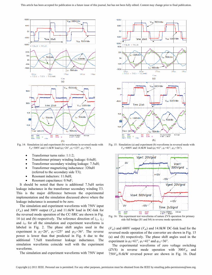
The simulation and experiment waveforms with 750V input (Vdc) and 300V output (Vds) and 11.6kW load in DC-link for the reversed mode operation of the CC-SRC are shown in Fig. 14 (a) and (b) respectively. The reference direction of iL1, iL2 and iT3 for all the simulation and experiment waveforms is labeled in Fig. 2. The phase shift angles used in the experiment is φ2=26°, φ1=125° and φ21=36°. The reverse power is lower than that predicted in Fig. 6 due to the additional 7.5uH transformer leakage inductance. The simulation waveforms coincide well with the experiment waveforms.
The simulation and experiment waveforms with 750V input
(Vdc) and 600V output (Vds) and 14.8kW DC-link load for the reversed mode operation of the converter are shown in Fig. 15 (a) and (b) respectively. The phase shift angles used in the experiment is φ2=61°, φ1=41° and φ21=36°.
The experimental waveforms of zero voltage switching (ZVS) in reverse mode operation with 300Vds and 750Vdc/8.6kW reversed power are shown in Fig. 16. Dual
Fig. 15: Simulation (a) and experiment (b) waveforms in reversed mode with
Vds=600V and 14.8kW load (φ2=61°, φ1=41°, φ21=36°).
Fig. 16: The experiment test waveforms of nature ZVS operation for primary
side full bridge (S1 and S4) in reverse mode operation.
Fig. 14: Simulation (a) and experiment (b) waveforms in reversed mode with
Vds=300V and 11.6kW load (φ2=26°, φ1=125°, φ21=36°).

Copyright (c) 2011 IEEE. Personal use is permitted. For any other purposes, permission must be obtained from the IEEE by emailing [email protected].
This article has been accepted for publication in a future issue of this journal, but has not been fully edited. Content may change prior to final publication.
power supply voltage (+15V and -15V) is used for the gate driver. For primary side bridge, nature ZVS is obtained and Fig. 16 shows the gate drive voltage Vge and output voltage Vce of S1 and S4. Auxiliary inductor and switches are required for secondary side IGBTs S7/8 to achieve ZVS at this load.
To verify the proposed modulation technique and LUT-based modulator, the converter transient response in reverse mode was simulated with close-loop feedback control. The effectiveness of simulation model was verified by Fig. 14 - Fig. 15. The DC-link voltage (Vdc) is sampled and regulated to 750V by a PI controller with the output connected to the input α of the LUT-based modulator (see Fig. 12). Vds is battery voltage. The load current in DC-link side (idc) switches between the half and full load. The waveforms of DC-link voltage, load current, AC voltage of primary and secondary full bridges, current in transformer primary and secondary windings, three phase-shift angles and the virtual phase-shift angle, at 300 Vds, are shown in Fig. 17.
Power loss models were built for each component in the converter to predict the efficiency in full load range. The calculated efficiency curves in forward mode with 300V and 600V output are shown in Fig. 18. The experimental tested efficiency points of 15kW prototype are also shown in Fig. 18, which indicate good agreement with the model prediction. From the medium to heavy load range, the efficiency ranges from 94%-96% with 600V output and 91%-92% with 300V output. It can be observed that the 300V output efficiency decreases at high power output. One possible reason is the large ratio of reactive current due to the high quality factor Q at heavy load (small Re) associated with lower Vds. Larger phase-shift angle φ1 is required for 300V output than for 600V at the same output power, which also injects more current to D11&12 and results in higher clamping circuit loss.
The calculated efficiency curves in reversed mode operation with 300V and 600V output are shown in Fig. 19. The efficiency curve with 600V output is calculated based on
the reverse modulation strategy 2. The experimental tested efficiency points of the prototype are also shown in Fig. 19. Compared to the forward mode the reverse mode efficiency drops about 2-3% from the medium to high power range. This is mainly due to the additional turn-off loss contributed by the secondary side IGBTs S5-S8. The efficiency drop at heavy load is observed as well for 300Vds. In reversed mode, the reactive power can be indicated by phase-shift angles. With 300V battery voltage, it is more difficult to reverse the power flow and the secondary side full bridge needs to lead the primary side by a larger angle at heavy load (φ21=90°). However, this angle also causes higher reactive power in the circuit, whereas for 600Vds, φ21 is only 36°.
The power loss breakdown analysis for the CC-SRC prototype in reverse mode with 300Vds/11.6kW is shown in Fig. 20. The conduction and turn-off loss of S3&S4 are larger than that of S1&S2 because from Fig. 14 the modulation strategy at 11.8kW reversed power results in higher current stress (iL2) in T2, L2, S3/D3 and S4/D4 branch than that (iL1) in T1, L1, S1/D1 and S2/D2 branch. But at high power or high output voltage level, the current unbalance is mitigated.
Fig. 18: The calculated and experiment tested efficiency in forward mode
with 300V and 600V output voltage of Vds (Vdc=750V).
Fig. 19: The calculated and experiment tested efficiency in reversed mode
with 300V and 600V output voltage of Vds (Vdc =750V).
Fig. 17: The simulated reverse mode transient response for DC-link load change with proposed modulation technique (Vds=300V, Vdc=750V).

Copyright (c) 2011 IEEE. Personal use is permitted. For any other purposes, permission must be obtained from the IEEE by emailing [email protected].
This article has been accepted for publication in a future issue of this journal, but has not been fully edited. Content may change prior to final publication.
VII. CONCLUSION
The series resonant DC-DC converter with clamped capacitor voltage (CC-SRC) exhibits excellent characteristics in forward mode, but single phase-shift angle control cannot reverse the power flow. The advanced modulation strategy based on three phase-shift angles is proposed to reverse the power flow and the optimum modulation trajectories with low and high output voltage in three-dimensional space are identified, based on the design of experiment and systematic numeric simulation approach. A LUT based digital modulator is proposed to simplify the angle control strategy. The proposed converter operation is verified by a scaled-down experimental prototype and the simulation waveforms coincide well with test waveforms. The converter efficiency is calculated and verified for bi-directional operation.
ACKNOWLEDGMENT
The authors would like to thank Professor Ming-Jun Lai at Department of Mathematics, University of Georgia for his generosity for providing us with his MATLAB programs of trivariate splines for data interpolation which are based on theory of multivariate splines.
REFERENCES [1] S. M. Lukic, J. Cao, R. C. Bansal, F. Rodriguez and A. Emadi, “Energy
storage systems for automotive applications,” in IEEE Transactions on Industrial Electronics, vol. 55, no. 6, pp. 2258–2267, Jun. 2008.
[2] S. Vazquez, S. M. Lukic, E. Galvan, L. G. Franquelo and J. M. Carrasco, “Energy storage systems for transport and grid applications,” in IEEE Transactions on Industrial Electronics, vol.57, no.12, pp.3881-3895, Dec. 2010.
[3] A. Emadi, Y. J. Lee and K. Rajashekara, “Power electronics and motor drives in electric, hybrid electric, and plug-in hybrid electric vehicles,” in IEEE Transactions on Industrial Electronics, vol. 55, no. 6, pp. 2237-2245, Jun. 2008.
[4] Z. Amjadi and S. S. Williamson, “Power-electronics-based solutions for plug-in hybrid electric vehicle energy storage and management systems,” in IEEE Transactions on Industrial Electronics, vol.57, no.2, pp.608-616, Feb. 2010.
[5] M. B. Camara, H. Gualous, F. Gustin, A. Berthon and B. Dakyo, “DC/DC converter design for supercapacitor and battery power management in hybrid vehicle applications—polynomial control strategy,” in IEEE Transactions on Industrial Electronics, vol.57, no.2, pp.587-597, Feb. 2010.
[6] M. Ortuzar, J. Moreno and J. Dixon, “Ultracapacitor-based auxiliary energy system for an electric vehicle: implementation and evaluation,” in IEEE Transactions on Industrial Electronics, vol.54, no.4, pp.2147-2156, Apr. 2007.
[7] Y. Du, X. Zhou, S. Bai, S. M. Lukic and A. Q. Huang, “Review of non-isolated bi-directional DC-DC converters for plug-in hybrid electric vehicles charge station application at municipal parking decks,” in IEEE 2010 Applied Power Electronics Conference and Exposition, pp. 1145-1151, Feb. 2010.
[8] W. Li, G. Joos and J. Belanger, “Real-Time simulation of a wind turbine generator coupled with a battery supercapacitor energy storage system,” in IEEE Transactions on Industrial Electronics, vol.57, no.4, pp.1137-1145, Apr. 2010.
[9] C. Abbey and G. Joos, “Supercapacitor energy storage for wind energy applications,” in IEEE Transactions on Industry Applications, vol.43, no.3, pp.769-776, May/Jun.2007.
[10] L. Qu and W. Qiao, “Constant power control of DFIG wind turbines with supercapacitor energy storage,” in IEEE Transactions on Industry Applications, vol.47, no.1, pp.359-367, Jan./Feb.2011.
[11] W. Jiang and B. Fahimi, “Active current sharing and source management in fuel cell–battery hybrid power system,” in IEEE Transactions on Industrial Electronics, vol.57, no.2, pp.752-761, Feb. 2010.
[12] T. Azib, O. Bethoux, G. Remy, C. Marchand and E. Berthelot, “An innovative control strategy of a single converter for hybrid fuel cell/supercapacitor power source,” in IEEE Transactions on Industrial Electronics, vol.57, no.12, pp.4024-4031, Dec.2010.
[13] A. S. Samosir and A. H. M. Yatim, “Implementation of dynamic evolution control of bidirectional DC–DC converter for interfacing ultracapacitor energy storage to fuel-cell system,” in IEEE Transactions on Industrial Electronics, vol.57, no.10, pp.3468-3473, Oct.2010.
[14] P. J. Grbovic, P. Delarue, P. Le Moigne and P. Bartholomeus, “A bidirectional three-level DC–DC converter for the ultracapacitor applications,” in IEEE Transactions on Industrial Electronics, vol.57, no.10, pp.3415-3430, Oct. 2010.
[15] K. Jin, M. Yang, X. Ruan and M. Xu, “Three-level bidirectional converter for fuel-cell/battery hybrid power system,” in IEEE Transactions on Industrial Electronics, vol.57, no.6, pp.1976-1986, Jun. 2010.
[16] H. Li, F. Z. Peng and J. S. Lawler, “A natural ZVS high-power bi- directional DC-DC converter with minimum number of devices,” in IEEE Transactions on Industry Applications, vol.39, no.2, pp.525-535, Mar./Apr. 2003.
[17] X. Li and A. K. S. Bhat, “Analysis and design of high-frequency isolated dual-bridge series resonant DC/DC converter,” in IEEE Transactions on Power Electronics, vol.25, no.4, pp.850-862, Apr.2010.
[18] S. Jalbrzykowski, A. Bogdan and T. Citko, “A dual full-bridge resonant Class-E bidirectional DC–DC converter,” in IEEE Transactions on Industrial Electronics, vol.58, no.9, pp.3879-3883, Sep. 2011.
[19] K. Wang, F. C. Lee and J. Lai, “Operation principles of bi-directional full-bridge DC/DC converter with unified soft-switching scheme and soft-starting capability,” in IEEE 2000 Applied Power Electronics Conference and Exposition, vol.1, pp.111-118, Feb.2000.
[20] L. Zhu, “A novel soft-commutating isolated boost full-bridge ZVS-PWM DC-DC converter for bidirectional high power applications,” in IEEE Transaction on Power Electronics, vol.21, no.2, pp.422-429,Mar. 2006.
[21] E. S. Kim, K. Y. Joe, H. Y. Choi, Y. H. Kim and Y. H. Cho, “An improved soft switching bi-directional PSPWM FB DC/DC converter,” in IEEE 1998 Annual Conference on Industrial Electronics Society, vol.2, pp.740-743, Aug.1998.
[22] R. W. De Doncker, D. M. Divan and M. H. Kheraluwala, “A three phase soft-switched high-power-density dc/dc converter for high-power applications,” in IEEE Transactions on Industry Applications, vol.27, no.1, pp.63-73, Jan./Feb.1991.
[23] S. Inoue and H. Akagi, “A bidirectional DC–DC converter for an energy storage system with galvanic isolation,” in IEEE Transactions on Power Electronics, vol.22, no.6, pp.2299-2306, Dec.2007.
[24] F. Krismer and J. W. Kolar, “Accurate power loss model derivation of a high-current dual active bridge converter for an automotive application,” in IEEE Transactions on Industrial Electronics, vol.57, no.3, pp.881-891, Mar. 2010.
[25] H. Bai and C. Mi, “Eliminate reactive power and increase system efficiency of isolated bidirectional dual-active-bridge DC-DC converters using novel dual-phase-shift control,” in IEEE Transactions on Power Electronics, vol.23, no.6, pp.2905-2914, Nov.2008.
Fig. 20: The power loss distribution for the 15kW prototype with 300Vds/11.6kW in reverse mode (total loss 2035W, Vdc=750V, Vds=300V).

Copyright (c) 2011 IEEE. Personal use is permitted. For any other purposes, permission must be obtained from the IEEE by emailing [email protected].
This article has been accepted for publication in a future issue of this journal, but has not been fully edited. Content may change prior to final publication.
[26] H. Zhou and A. M. Khambadkone, “Hybrid modulation for dual-active-bridge bidirectional converter with extended power range for ultracapacitor application,” in IEEE Transactions on Industry Applications, vol.45, no.4, pp.1434-1442, Jul./Aug. 2009.
[27] A. K. Jain and R. Ayyanar, “PWM control of dual active bridge-comprehensive analysis and experimental verification,” in IEEE Transactions on Power Electronics, vol.26, no.4, pp.1215-1227, Apr. 2011.
[28] G. G. Oggier, G. O. García and A. R. Oliva, “Modulation strategy to operate the dual active bridge DC–DC converter under soft switching in the whole operating range,” in IEEE Transactions on Power Electronics, vol.26, no.4, pp.1228-1236, Apr. 2011.
[29] B. S. Jacobson and R. A. DiPerna, “Series resonant converter with clamped tank capacitor voltage,” in IEEE 1990 Applied Power Electronics Conference and Exposition, pp.137-146, Mar.1990.
[30] B. S. Jacobson and R. A. DiPerna, “Design of a series resonant converter with clamped capacitor voltage and anti-cross-conduction inductors,” in IEEE 1998 Applied Power Electronics Conference and Exposition, vol.2, pp.829 – 833, Feb.1998.
[31] B. S. Jacobson, J. McGainty and P. C. Thomas, “Method and apparatus for a power system for phased-array radar,” United States Patent, No. 6,856,283, Feb.2005.
[32] T. Kato and G. C. Verhgese, “Efficient numerical determination of boundaries between operating modes of a power converter,” in IEEE 1992 Workshop on Computers in Power Electronics, pp. 205 – 216, Aug.1992.
[33] T. T. J. Ho, G. C. Verghese, C. Osawa, B. S. Jacobson and T. Kato, “Dynamic modeling, simulation and control of a series resonant converter with clamped capacitor voltage,” in IEEE 1994 Power Electronics Specialists Conference, vol.2, pp.1289-1296, Jun.1994.
[34] Y. Du, X. Bian, S. M. Lukic, B. S. Jacobson and A. Q. Huang, “A novel wide voltage range bi-directional series resonant converter with clamped capacitor voltage,” in IEEE 2009 Annual Conference of Industrial Electronics Society, pp.82-87, Nov.2009.
[35] G. Awanou, M. J. Lai, and P. Wenston, “The multivariate spline method for numerical solution of partial differential equations and scattered data interpolation,” in Wavelets and Splines: Athens 2005, edited by G. Chen and M. J. Lai, Nashboro Press, 2006, pp.24-74.
[36] R. W. Erikson and D. Maksimovic, “Fundamentals of Power Electronics,” 2nd ed. Kluwer Academic Publishers, 2001, pp.705-718.
Yu Du (S’10) was born in Chengdu, Sichuan, China. He received the B.S. and M.S. degrees in electrical engineering (power electronics) in 2002 and 2005 respectively, from the Department of Electrical Engineering at Zhejiang University, Hangzhou, China.
From 2005 to 2007, he was with Global Research Center (Shanghai, China) of General Electric Company (GE). He developed medical power supplies for GE Healthcare and conducted
interdisciplinary research on novel electric-driven desalination process. He is the recipient of 2006 Global Research Rookie Award.
Since 2007, Mr. Du has been working towards his PhD degree in NSF FREEDM Systems ERC at North Carolina State University, Raleigh. He was exchanged to the Power Electronics Systems Lab at ETH-Zurich, Switzerland for three-month research. His research interests include ultra-compact bi-directional converters, high voltage converters and distributed energy storage systems. He holds 6 U.S. patents and has two U.S. patents pending.
Srdjan M. Lukic (S’02–M’07) received the M.S. and Ph.D. degrees in electrical engineering from the Illinois Institute of Technology, Chicago, in 2004 and 2007, respectively.
From 2002 to 2004, he was with Firefly Energy Inc., where he was responsible for optimizing certain aspects of carbon/graphite foam-based lead acid batteries for novel automotive applications. He is currently an Assistant Professor in the Department of Electrical and Computer Engineering, North
Carolina State University, Raleigh. He serves as a Faculty Member and Testbed Leader for plug-in hybrid electric vehicles in the Future Renewable Electric Energy Delivery and Management Systems Engineering Research Center. His research interests are broadly in the field of power electronics and motor drives applied to electric energy storage systems, electric vehicle drivetrains, and inductive power transfer systems.
Boris S. Jacobson received a Diploma in electrical engineering (power electronics) in 1974 from St. Petersburg Electrotechnical University, St. Petersburg, Russia and a MSEE (systems) degree in 1989 from the University of Lowell, Lowell, MA. He has 36 years of experience in such power electronics areas as plasma arc treatment, mining, medical equipment, data processing, military electronics and shipboard systems. He joined Raytheon Company in 1987 where he works on
power systems and converters and consults throughout Raytheon. Currently, he works as Technical Director for the Compact Power
Conversion Technologies (CPCT) program (Office of Naval Research). The CPCT effort changes paradigm for shipboard power systems and Micro-Grids. His area of expertise covers systems, grounding methods, low-noise system, high frequency converters and magnetics. He published 18 papers and has 12 patents in the fields of converters topologies, system architectures and magnetic devices.
Boris is a Senior Member of IEEE and serves on several IEEE Standards committees including IEEE Guide for Recommended Practice for Electrical Installations on Shipboard - Systems Integration and IEEE Guide for Control Architecture for High Power Electronics (1 MW and Greater) used in Electric Power Transmission and Distribution Systems. He served on Technical Committees of for ASNE Day Conference, IEEE Electric Ship Technologies Symposiums.
Alex Q. Huang (Fellow, IEEE) was born in Zunyi, Guizhou, China. He received the B.Sc. degree from Zheijiang University, Hangzhou, China, in 1983 and the M.Sc. degree from Chengdu Institute of Radio Engineering, Chengdu, China, in 1986, both in electrical engineering, and the Ph.D. degree in electrical engineering from Cambridge University, Cambridge, U.K., in 1992.
From 1992 to 1994, he was a Research Fellow at Magdalene College, Cambridge, U.K. From 1994 to
2004, he was a Professor at the Bradley Department of Electrical and Computer Engineering, Virginia Polytechnic Institute and State University, Blacksburg. Since 2004, he has been with North Carolina State University, Raleigh, and is currently the Progress Energy Distinguished Professor of Electrical and Computer Engineering and directs the NSF FREEDM Systems ERC, NCSU Advanced Transportation Energy Center (ATEC). Since 1983, he has been involved in the development of modern power semiconductor devices and power integrated circuits. He fabricated the first IGBT power device in China in 1985. He is the inventor and key developer of the emitter turnoff thyristor technology. His current research interests are utility power electronics, power management microsystems, and power semiconductor devices. He has published more than 200 papers in the international conferences and journals, and has 14 U.S. patents.
Dr. Huang is the recipient of the National Science Foundation (NSF) CAREER award and the prestigious R&D 100 Award.