Embed Size (px)
Citation preview
Molded transparent photopolymers and phase shift optics for fabricating three dimensional
nanostructures Seokwoo Jeon1, Daniel J. Shir1, Yun Suk Nam1, Robert Nidetz1, Matthew Highland1,
David G. Cahill1, John A. Rogers*1, Mehmet F. Su2, Ihab F. El-Kady2,3, Christos G. Christodoulou2, and Gregory R. Bogart3
1 Department of Materials Science and Engineering, Electrical and Computer Engineering, and Chemistry, Beckman Institute and Seitz Materials Research Laboratory, University of Illinois, Urbana, IL 61801
2 Department of Electrical and Computer Engineering, University of New Mexico, Albuquerque, NM 87131 3 Sandia National Laboratory, Albuquerque, NM 87185
*Corresponding author: [email protected]
Abstract: This paper introduces approaches that combine micro/nanomolding, or nanoimprinting, techniques with proximity optical phase mask lithographic methods to form three dimensional (3D) nanostructures in thick, transparent layers of photopolymers. The results demonstrate three strategies of this type, where molded relief structures in these photopolymers represent (i) fine (<1 μm) features that serve as the phase masks for their own exposure, (ii) coarse features (>1 μm) that are used with phase masks to provide access to large structure dimensions, and (iii) fine structures that are used together phase masks to achieve large, multilevel phase modulations. Several examples are provided, together with optical modeling of the fabrication process and the transmission properties of certain of the fabricated structures. These approaches provide capabilities in 3D fabrication that complement those of other techniques, with potential applications in photonics, microfluidics, drug delivery and other areas.
© 2007 Optical Society of America OCIS codes: (220.4000) Microstructure fabrication; (320.7110) Ultrafast nonlinear optics; (050.0050) Diffraction and gratings
References and links
1. P. J. A. Kenis, R. F. Ismagilov, and G. M. Whitesides, "Microfabrication inside capillaries using multiphase laminar flow patterning," Science 285, 83-85 (1999).
2. Y. N. Xia and G. M. Whitesides, "Soft lithography," Angew. Chem., Int. Ed. Engl. 37, 551-575 (1998). 3. D. G. Grier, "A revolution in optical manipulation," Nature 424, 810-816 (2003). 4. D. N. Christodoulides, F. Lederer, and Y. Silberberg, "Discretizing light behavior in linear and nonlinear
waveguide lattices," Nature 424, 817-823 (2003). 5. J. H. Holtz and S. A. Asher, "Polymerized colloidal crystal hydrogel films as intelligent chemical sensing
materials," Nature 389, 829-832 (1997). 6. J. W. Long, B. Dunn, D. R. Rolison, and H. S. White, "Three-Dimensional Battery Architectures," Chem.
Rev. 104, 4463-4492 (2004). 7. B. T. Holland, C. Blanford, and A. Stein, "Synthesis of macroporous minerals with highly ordered three-
dimensional arrays of spheroidal voids," Science 281, 538-540 (1998). 8. B. H. Cumpston, S. P. Ananthavel, S. Barlow, D. L. Dyer, J. E. Ehrlich, L. L. Erskine, A. A. Heikal, S. M.
Kuebler, I. Y. S. Lee, D. McCord-Maughon, J. Qin, H. Rockel, M. Rumi, X.-L. Wu, S. R. Marder, and J. W. Perry, "Two-photon polymerization initiators for three-dimensional optical data storage and microfabrication," Nature 398, 51-54 (1999).
9. S. Uemura, "The activities of FGM on new application," Mater. Sci. Forum 423-425(Functionally Graded Materials VII), 1-10 (2003).
10. B. Kaehr and J. B. Shear, "Mask-Directed Multiphoton Lithography," J. Am. Chem. Soc. 129 1904-1905 (2007).
11. D. B. Shao and S. C. Chen, "Direct patterning of three-dimensional periodic nanostructures by surface-plasmon-assisted nanolithography," Nano. Lett. 6, 2279-2283 (2006).
#80994 - $15.00 USD Received 13 Mar 2007; revised 3 May 2007; accepted 3 May 2007; published 8 May 2007
(C) 2007 OSA 14 May 2007 / Vol. 15, No. 10 / OPTICS EXPRESS 6358
12. S. Jeon, V. Malyarchuk, J. O. White, and J. A. Rogers, "Optically fabricated three dimensional nanofluidic mixers for microfluidic devices," Nano. Lett. 5, 1351-1356 (2005).
13. S. Jeon, J.-U. Park, R. Cirelli, S. Yang, C. E. Heitzman, P. V. Braun, P. J. A. Kenis, and J. A. Rogers, "Fabricating complex three-dimensional nanostructures with high-resolution conformable phase masks," Proc. Natl. Acad. Sci. U. S. A. 101, 12428-12433 (2004).
14. W. Zhou, Y. Huang, E. Menard, N. R. Aluru, J. A. Rogers, and A. G. Alleyne, "Mechanism for stamp collapse in soft lithography," Appl. Phys. Lett. 87 251925 (2005).
15. K. J. Hsia, Y. Huang, E. Menard, J. U. Park, W. Zhou, J. Rogers, and J. M. Fulton, "Collapse of stamps for soft lithography due to interfacial adhesion," Appl. Phys. Lett. 86, 154106 (2005).
16. S. Jeon, Y. Nam, D. Shir, J. Rogers, and A. Hamza, "three dimensional nanoporous density graded materials formed by optical exposures through conformable phase masks’," Appl. Phys. Lett. 89, 253101 (2006).
17. S. Jeon, V. Malyarchuk, J. A. Rogers, and G. P. Wiederrecht, "Fabricating three dimensional nanostructures using two photon lithography in a single exposure step," Opt. Express 14, 2300-2308 (2006).
18. K. E. Paul, T. L. Breen, J. Aizenberg, and G. M. Whitesides, "Maskless photolithography: Embossed photoresist as its own optical element," Appl. Phys. Lett. 73, 2893-2895 (1998).
19. K. E. Paul, T. L. Breen, T. Hadzik, G. M. Whitesides, S. P. Smith, and M. Prentiss, "Imaging patterns of intensity in topographically directed photolithography," J. Vac. Sci. Technol. B 23, 918-925 (2005).
20. F. Hua, Y. G. Sun, A. Gaur, M. A. Meitl, L. Bilhaut, L. Rotkina, J. F. Wang, P. Geil, M. Shim, J. A. Rogers, and A. Shim, "Polymer imprint lithography with molecular-scale resolution," Nano. Lett. 4, 2467-2471 (2004).
21. "The GSOLVER ver. 4.20 developed by Grating Solver Development Company (P.O. Box 353, Allen, TX 75013)."
22. H. Tan, A. Gilbertson, and S. Y. Chou, "Roller nanoimprint lithography," J. Vac. Sci. Technol. B 16, 3926-3928 (1998).
23. L. F. Li, "Formulation and comparison of two recursive matrix algorithms for modeling layered diffraction gratings," J. Opt. Soc. Am. A 13, 1024-1035 (1996).
24.
1. Introduction
Applications of three dimensional (3D) nanostructures in microfluidics, [1, 2] photonics, [3, 4] sensors, [5] fuel cells and battery devices, [6] catalyst supports, [7] data storage materials, [8] and density gradient systems [9] create interest in the development of methods for fabricating such structures. Many techniques exist, although most have disadvantages, including some combination of slow patterning speeds, limited structure geometries, experimentally inconvenient setups, and difficult scale-up to large areas. Methods that use three dimensional optical techniques with phase and/or amplitude masking elements can be relatively simple to use, they can involve parallel, high speed (i.e. single exposure) operation and they can be applied to large areas [10, 11]. One such method, which we refer to as proximity field nanoPatterning (PnP), [12, 13] uses conformable, elastomeric phase masks to pattern thick, transparent layers of photosensitive materials. This approach involves a contact exposure geometry achieved through the action of generalized adhesion forces that pull the mask into atomic-scale, conformal contact with the photosensitive layer [14, 15]. Light passing through the mask creates a three dimensional distribution of intensity in proximity to its surface that exposes the photosensitive layer through its thickness [13]. Removing the regions of material that have (or have not, depending on the chemistry) been exposed yields a solid form, 3D replica of the intensity distribution. The optics of this system, which involves self-imaging and Talbot effects, determines the geometries of these 3D structures. The layout of the mask and its optical properties, the coherence, wavelength and directionality of the exposure light, the optical properties of the photosensitive material and the nature of its interaction with the exposure light (e.g. one or multi photon effects) represent some of the parameters that can be controlled to yield structures with certain desired 3D shapes. Although many varied classes of periodic and aperiodic 3D structures have been demonstrated [12, 13, 16, 17], important limitations remain.
This paper presents methods that extend the range of structures that can be formed by PnP and related approaches. The results introduce, in particular, methods for using molding, or nanoimprinting, techniques to form patterns of relief in photosensitive materials that can be used in combination with, or as replacements for, the masking optics. This strategy provides important additional flexibility in the patterning process that can be exploited to yield 3D structures with potential applications in photonics and other areas. In one version of this
#80994 - $15.00 USD Received 13 Mar 2007; revised 3 May 2007; accepted 3 May 2007; published 8 May 2007
(C) 2007 OSA 14 May 2007 / Vol. 15, No. 10 / OPTICS EXPRESS 6359
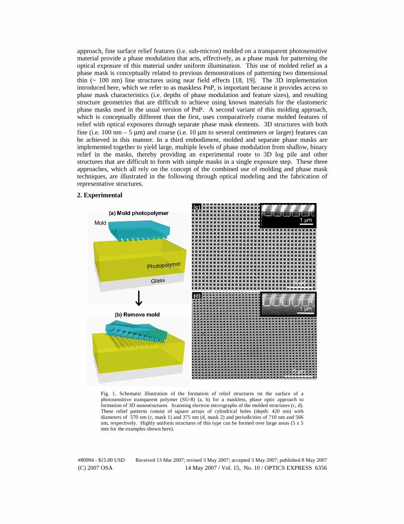
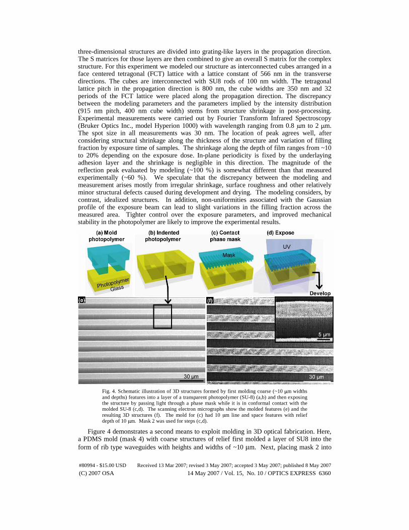
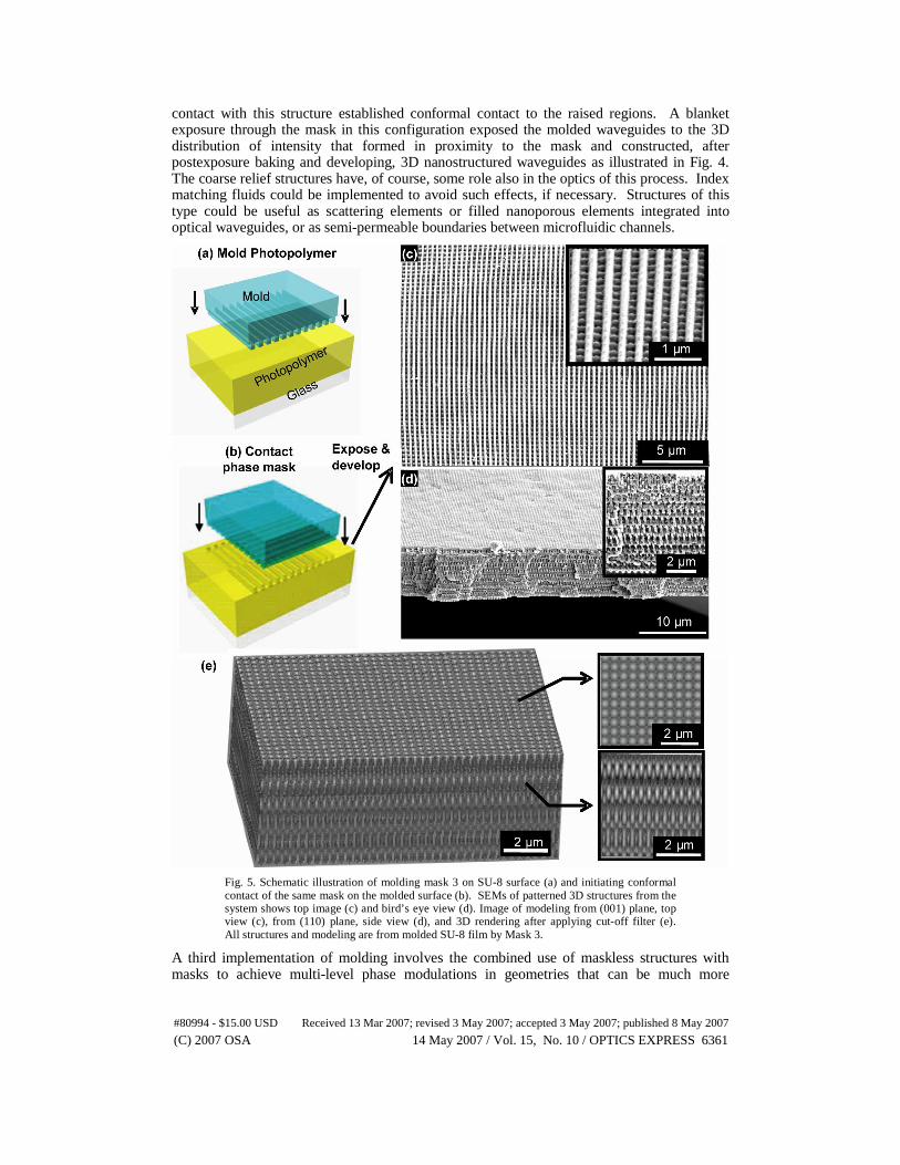
approach, fine surface relief features (i.e. sub-micron) molded on a transparent photosensitive material provide a phase modulation that acts, effectively, as a phase mask for patterning the optical exposure of this material under uniform illumination. This use of molded relief as a phase mask is conceptually related to previous demonstrations of patterning two dimensional thin (~ 100 nm) line structures using near field effects [18, 19]. The 3D implementation introduced here, which we refer to as maskless PnP, is important because it provides access to phase mask characteristics (i.e. depths of phase modulation and feature sizes), and resulting structure geometries that are difficult to achieve using known materials for the elastomeric phase masks used in the usual version of PnP. A second variant of this molding approach, which is conceptually different than the first, uses comparatively coarse molded features of relief with optical exposures through separate phase mask elements. 3D structures with both fine (i.e. 100 nm – 5 μm) and coarse (i.e. 10 μm to several centimeters or larger) features can be achieved in this manner. In a third embodiment, molded and separate phase masks are implemented together to yield large, multiple levels of phase modulation from shallow, binary relief in the masks, thereby providing an experimental route to 3D log pile and other structures that are difficult to form with simple masks in a single exposure step. These three approaches, which all rely on the concept of the combined use of molding and phase mask techniques, are illustrated in the following through optical modeling and the fabrication of representative structures.
2. Experimental
Fig. 1. Schematic illustration of the formation of relief structures on the surface of a photosensitive transparent polymer (SU-8) (a, b) for a maskless, phase optic approach to formation of 3D nanostructures. Scanning electron micrographs of the molded structures (c, d). These relief patterns consist of square arrays of cylindrical holes (depth: 420 nm) with diameters of 570 nm (c, mask 1) and 375 nm (d, mask 2) and periodicities of 710 nm and 566 nm, respectively. Highly uniform structures of this type can be formed over large areas (5 x 5 mm for the examples shown here).
#80994 - $15.00 USD Received 13 Mar 2007; revised 3 May 2007; accepted 3 May 2007; published 8 May 2007
(C) 2007 OSA 14 May 2007 / Vol. 15, No. 10 / OPTICS EXPRESS 6360
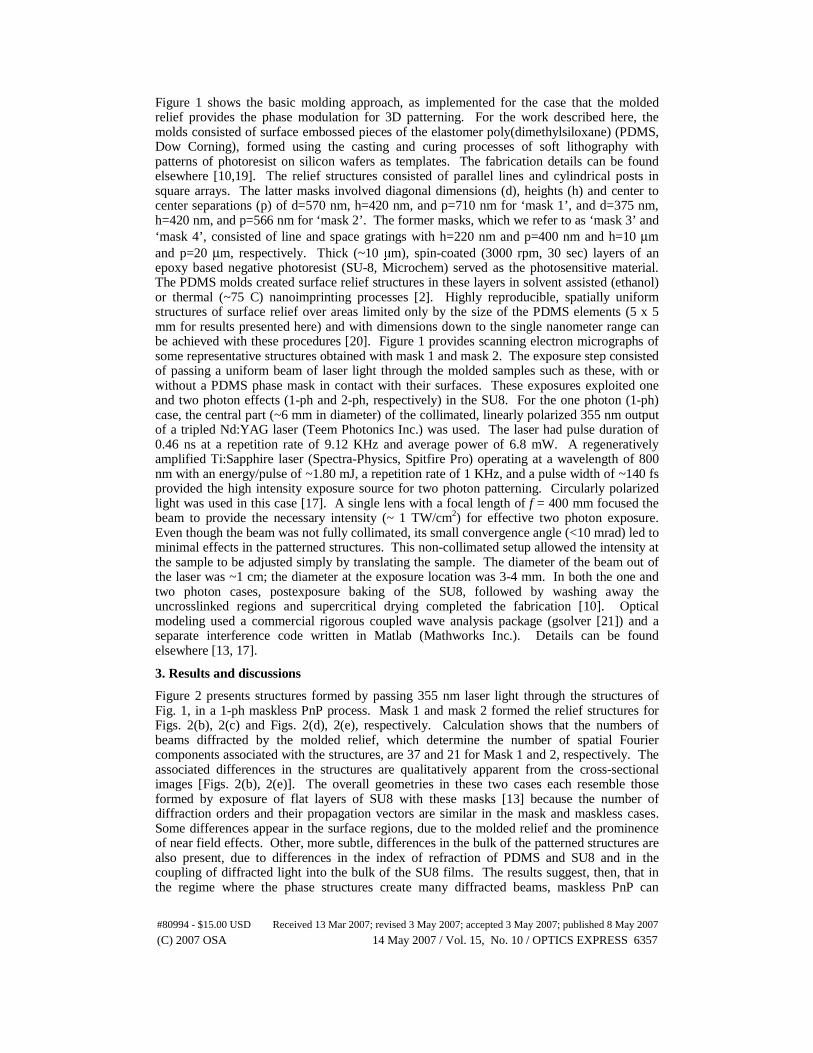
Figure 1 shows the basic molding approach, as implemented for the case that the molded relief provides the phase modulation for 3D patterning. For the work described here, the molds consisted of surface embossed pieces of the elastomer poly(dimethylsiloxane) (PDMS, Dow Corning), formed using the casting and curing processes of soft lithography with patterns of photoresist on silicon wafers as templates. The fabrication details can be found elsewhere [10,19]. The relief structures consisted of parallel lines and cylindrical posts in square arrays. The latter masks involved diagonal dimensions (d), heights (h) and center to center separations (p) of d=570 nm, h=420 nm, and p=710 nm for ‘mask 1’, and d=375 nm, h=420 nm, and p=566 nm for ‘mask 2’. The former masks, which we refer to as ‘mask 3’ and ‘mask 4’, consisted of line and space gratings with h=220 nm and p=400 nm and h=10 μm and p=20 μm, respectively. Thick (~10 μm), spin-coated (3000 rpm, 30 sec) layers of an epoxy based negative photoresist (SU-8, Microchem) served as the photosensitive material. The PDMS molds created surface relief structures in these layers in solvent assisted (ethanol) or thermal (~75 C) nanoimprinting processes [2]. Highly reproducible, spatially uniform structures of surface relief over areas limited only by the size of the PDMS elements (5 x 5 mm for results presented here) and with dimensions down to the single nanometer range can be achieved with these procedures [20]. Figure 1 provides scanning electron micrographs of some representative structures obtained with mask 1 and mask 2. The exposure step consisted of passing a uniform beam of laser light through the molded samples such as these, with or without a PDMS phase mask in contact with their surfaces. These exposures exploited one and two photon effects (1-ph and 2-ph, respectively) in the SU8. For the one photon (1-ph) case, the central part (~6 mm in diameter) of the collimated, linearly polarized 355 nm output of a tripled Nd:YAG laser (Teem Photonics Inc.) was used. The laser had pulse duration of 0.46 ns at a repetition rate of 9.12 KHz and average power of 6.8 mW. A regeneratively amplified Ti:Sapphire laser (Spectra-Physics, Spitfire Pro) operating at a wavelength of 800 nm with an energy/pulse of ~1.80 mJ, a repetition rate of 1 KHz, and a pulse width of ~140 fs provided the high intensity exposure source for two photon patterning. Circularly polarized light was used in this case [17]. A single lens with a focal length of f = 400 mm focused the beam to provide the necessary intensity (~ 1 TW/cm2) for effective two photon exposure. Even though the beam was not fully collimated, its small convergence angle (<10 mrad) led to minimal effects in the patterned structures. This non-collimated setup allowed the intensity at the sample to be adjusted simply by translating the sample. The diameter of the beam out of the laser was ~1 cm; the diameter at the exposure location was 3-4 mm. In both the one and two photon cases, postexposure baking of the SU8, followed by washing away the uncrosslinked regions and supercritical drying completed the fabrication [10]. Optical modeling used a commercial rigorous coupled wave analysis package (gsolver [21]) and a separate interference code written in Matlab (Mathworks Inc.). Details can be found elsewhere [13, 17].
3. Results and discussions
Figure 2 presents structures formed by passing 355 nm laser light through the structures of Fig. 1, in a 1-ph maskless PnP process. Mask 1 and mask 2 formed the relief structures for Figs. 2(b), 2(c) and Figs. 2(d), 2(e), respectively. Calculation shows that the numbers of beams diffracted by the molded relief, which determine the number of spatial Fourier components associated with the structures, are 37 and 21 for Mask 1 and 2, respectively. The associated differences in the structures are qualitatively apparent from the cross-sectional images [Figs. 2(b), 2(e)]. The overall geometries in these two cases each resemble those formed by exposure of flat layers of SU8 with these masks [13] because the number of diffraction orders and their propagation vectors are similar in the mask and maskless cases. Some differences appear in the surface regions, due to the molded relief and the prominence of near field effects. Other, more subtle, differences in the bulk of the patterned structures are also present, due to differences in the index of refraction of PDMS and SU8 and in the coupling of diffracted light into the bulk of the SU8 films. The results suggest, then, that in the regime where the phase structures create many diffracted beams, maskless PnP can
#80994 - $15.00 USD Received 13 Mar 2007; revised 3 May 2007; accepted 3 May 2007; published 8 May 2007
(C) 2007 OSA 14 May 2007 / Vol. 15, No. 10 / OPTICS EXPRESS 6361
provide an alternative route of patterning when direct conformal contact of phase mask to patterning material is not feasible. Also, the molding process can be implemented in ways that are inconvenient with masks. For example, molding with a small mold in a step-and-repeat fashion or with a cylindrical mold in a continuous reel-to-reel setup [22] can yield processed films that are suitable for large area maskless patterning in a single exposure step.
Fig. 2. Schematic illustration (a) of optical exposure through the molded surface of a transparent layer of a photopolymer (SU-8). Cross-sectional (b, e) and top view (c, d) scanning electron micrographs of 3D nanostructures by developing away unexposed regions of the polymer. Mask 1 and 2 were used for (b, c) and (d, e), respectively.
The value of the maskless approach in producing structure geometries that are not easily achieved using the mask based technique is most clearly evident when applied in a 2-ph patterning mode. Previous work [17] reported body centered tetragonal structures produced by 2-ph PnP with 810 nm fs pulsed exposure light and a phase mask with h=510 nm, d=570 nm and p=710 nm. Similar structures with face centered cubic geometries would require a mask with a much shorter period, p ~ 540 nm. The fabrication challenges associated with creating an elastomeric mask that has this geometry and, at the same time, offers sufficient depth of relief to provide adequate phase shifting are extreme. Mechanical instabilities and fracture of relief features in typical elastomers make sub-micron features with aspect ratios of larger than ~2x are difficult to produce reliably. Classes of elastomers (e.g. PDMS or perfluoropolyether) that have been used for phase masks have indices of refraction in the range of 1.34-1.4. These two considerations lead to masks with the lateral layout of mask 2, for example, that can provide, at most, phase shifts of up to ~ 0.5π. Mask 2 offers such a small phase modulation (i.e. ~0.4π) that the intensity contrast (
minmax / II ) of the 3D intensity
distribution that forms in the photoresist with 800 nm light is only <6, even in 2-ph mode. The maskless approach avoids this problem because it transfers relief structure from the
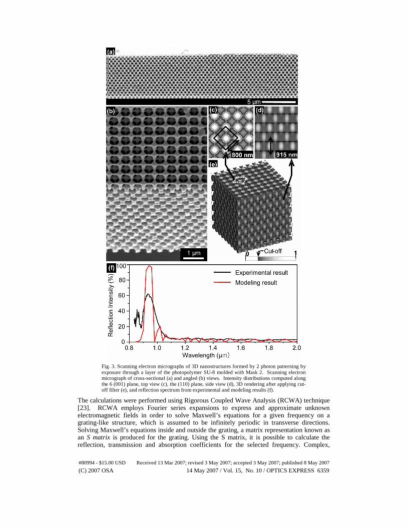
elastomeric masks into the photosensitive materials, which can be designed with comparatively high index of refraction. The index of SU8 is, for example, ~1.58. This value leads to a phase modulation of ~0.63π and a intensity contrast of >50 in the same 2-ph mode. Figure 3 presents a representative 3D patterning result, together with optical modeling of the intensity distribution. This structure has close to face centered cubic (FCC) symmetry, with lattice parameters of 800 nm in-plane [Fig. 3(c)] and 915 nm out-of-plane [Fig. 3(d)], both in good agreement with modeling. These types of layouts might have possible applications and wavelength selective filters and, if used as templates for the growth of high index materials, as photonic bandgap structures. The bottom frame of Fig. 3 illustrates some measurements and calculations of transmission of light passing through a representative structure in a direction parallel to its surface normal.
#80994 - $15.00 USD Received 13 Mar 2007; revised 3 May 2007; accepted 3 May 2007; published 8 May 2007