Embed Size (px)
Citation preview

1
MOLYBDENUM-TRIOXIDE ASSISTED CHARGE INJECTION FROM METAL ANODES INTO ORGANIC LIGHT EMITTING DIODES
By MIKAIL A. SHAIKH
A THESIS PRESENTED TO THE GRADUATE SCHOOL OF THE UNIVERSITY OF FLORIDA IN PARTIAL FULFILLMENT
OF THE REQUIREMENTS FOR THE DEGREE OF MASTER OF SCIENCE
UNIVERSITY OF FLORIDA
2009

2
© 2009 Mikail A. Shaikh

3
To my mother, Zarin, the rock on which I stand tall
4
ACKNOWLEDGMENTS
I am eternally grateful to those who care. My parents top the list, my father being my
counsel and inspiration in the face of chaos and the epitome of hard work, and my mother, who
believed in me even when I faltered. The sacrifice they made of allowing their eldest to fly away
and pursue a dream. I pray I am so strong. I’d also like to name, among others, Jasmine, a friend
beyond measure, and my greatest treasure.
I’d like to express my sincere gratitude and respect for Dr. Franky So, my graduate
advisor, for giving me the right kind of nudge in the right direction at the right time. I also cannot
pass lightly over the influence of Jaewon, Kaushik, Neetu and all the other people of the Organic
Electronics group. I appreciate them being there.

5
TABLE OF CONTENTS page
ACKNOWLEDGMENTS.................................................................................................................... 4
LIST OF TABLES................................................................................................................................ 8
LIST OF FIGURES .............................................................................................................................. 9
ABSTRACT ........................................................................................................................................ 11
CHAPTER
1 INTRODUCTION....................................................................................................................... 13
Introduction ................................................................................................................................. 13 Purpose of this Study .................................................................................................................. 13 Historical Review ........................................................................................................................ 14 Theory of Electroluminescence .................................................................................................. 15 Device Architectures ................................................................................................................... 17
2 LITERATURE REVIEW-HOLE INJECTION INTO ORGANIC SEMICONDUCTORS ................................................................................................................ 19
Introduction ................................................................................................................................. 19 Conceptual Aspects ..................................................................................................................... 19
Electronic Structure ............................................................................................................. 19 Energy Alignment at a Metal-Organic Interface ............................................................... 20 Band Bending in an Organic Layer .................................................................................... 21 Application of Ultraviolet Photoelectron Spectroscopy in the Study of Interfaces......... 22
Relevant Metal-Organic Interfaces ............................................................................................ 23 NPB/Alq3 Interface .............................................................................................................. 23 Alq3 / LiF / Al Interfaces ..................................................................................................... 24
Review of Hole-Injection Materials ........................................................................................... 25 Indium Tin Oxide (ITO) Anodes ........................................................................................ 25 Copper Phthalocyanine as a Hole Injection Material ........................................................ 26 Polymeric Anodes as Ohmic Contacts for NPB: ............................................................... 27 Nickel Oxide as a transparent p-type Conducting Oxide .................................................. 27 Conducting/Insulating Nature of WO3 ............................................................................... 28 Charge Injection through Plasma Polymerized Fluorocarbon Films ............................... 28 The Use of MoO3 as an Anode Buffer Layer..................................................................... 29
3 LITERATURE REVIEW-ALTERNATE MATERIALS FOR ANODES ............................. 41
Charge Injection .......................................................................................................................... 41 Introduction .......................................................................................................................... 41 Conventional Approach to Carrier Injection ...................................................................... 41

6
Observed Electron Injection from Cathodes ...................................................................... 42 The Interface Injection Model ............................................................................................ 43 Carrier Injection into α-NPB .............................................................................................. 44
Review of Alternate Anodes ................................................................................................... 45 Introduction .......................................................................................................................... 45 Use of p-Type Silicon .......................................................................................................... 45 Semitransparent Silver Anode ............................................................................................ 46 Metal / Fullerene Electrodes ............................................................................................... 46 Oxides Of Underlying Metal Anodes as Effective Hole Injection Contacts ................... 47 Charge Generation Interfaces.............................................................................................. 48 Feasibility of a Metal Anode using Molybdenum Trioxide .............................................. 49
4 EXPERIMENTAL METHODS ................................................................................................. 57
Introduction ................................................................................................................................. 57 Device Preparation ...................................................................................................................... 57
Substrate Cleaning ............................................................................................................... 57 Surface Treatment ................................................................................................................ 58 Addition of Polymeric Hole-Injection Layer ..................................................................... 58 Thermal Evaporation ........................................................................................................... 59 Encapsulation ....................................................................................................................... 60
Device Materials and Architecture............................................................................................. 60 Characterization Techniques ...................................................................................................... 61
LIV Measurements .............................................................................................................. 61 Sample Holder ..................................................................................................................... 61 Analysis of Spectrum .......................................................................................................... 62 Capacitance Voltage Measurements ................................................................................... 62
Experimental Procedure .............................................................................................................. 63 Thickness Variation of the Molybdenum Oxide Hole Injection Layer ............................ 63 Study of Metallic Anodes .................................................................................................... 63 Lifetime Measurement of OLEDs ...................................................................................... 63
5 RESULTS AND DISCUSSION ................................................................................................ 70
Molybdenum Oxide as a Hole-Injection Material for Green OLEDs...................................... 70 Background .......................................................................................................................... 70 Results .................................................................................................................................. 70 Discussion ............................................................................................................................ 71
Metal-Based Composite Anodes ................................................................................................ 73 Background .......................................................................................................................... 73 Results .................................................................................................................................. 73 Discussion ............................................................................................................................ 75
Lifetime and Degradation of OLEDs Based on the Performance of Hole-Injection Materials................................................................................................................................... 78
Background .......................................................................................................................... 78 Results .................................................................................................................................. 78 Discussion ............................................................................................................................ 79

7
6 SUMMARY AND FUTURE WORK ....................................................................................... 91
Summary of Results .................................................................................................................... 91 Future Work ................................................................................................................................. 92
REFERENCES ................................................................................................................................... 95
BIOGRAPHICAL SKETCH ........................................................................................................... 100

8
LIST OF TABLES
Table page 4-1 Specification of Organic materials and films ....................................................................... 65
4-2 Specifications of Metals and films ........................................................................................ 65
4-3 Structures of Organic Compounds ........................................................................................ 65

9
LIST OF FIGURES
Figure page 1-1 Schematic of the theory of Electroluminescence ................................................................. 18
2-1 Plot of Coulombic Energy versus distance for nucleus ....................................................... 32
2-2 Vacuum level at infinity and close to the solid .................................................................... 32
2-3 Interface formation between a metal and an organic material ............................................ 33
2-4 Band Bending at a metal / organic interface......................................................................... 34
2-5 UPS diagram of energy levels of metal and overlaid organic material .............................. 34
2-6 Energy level offset at NPB/Alq3 interface ............................................................................ 35
2-7 Energy Offset at the Alq3/LiF/Al interface........................................................................... 36
2-8 Energy level alignment of ITO, CuPc and PEDOT to NPB ................................................ 37
2-9 Formation of Ohmic Contact of NPB with PEDOT ............................................................ 37
2-10 Transmission through MoO3 and CuPc based films on NPB .............................................. 38
2-11 AFM images showing surface roughness ............................................................................. 38
2-12 UPS data for ITO, ITO/NPB, ITO/CuPc, ITO/MoO3, ITO/MoO3:NPB ............................ 39
2-13 UPS data for ITO/NPB, ITO/CuPc/NPB, ITO/MoO3/NPB, ITO/MoO3:NPB/NPB ......... 39
2-14 Energy diagram showing offsets for ITO/NPB, ITO/CuPC, ITO/MoO3/NPB and ITO/MoO3:NPB/NPB ............................................................................................................ 40
2-15 XPS data showing energy shift of Indium 3d peaks ............................................................ 40
3-1 Electron injection from various cathodes into Alq3 ............................................................. 51
3-2 Electron Injection from various cathodes at 30K and 290K ............................................... 51
3-3 Interface Injection Model, showing the energy diagram modified by interfacial states caused by dipoles (a), (b) and the energy distribution for the first few layers of the organic material (c). ............................................................................................................... 52
3-4 Inductance spectroscopy of ITO/NPB showing filling and depopulation at different bias voltages ........................................................................................................................... 53
3-5 Energy diagram of (a)p-Si/TPD and (b) ITO/TPD ............................................................. 54

10
3-6 Energy diagram of Au/HAT-CN/NPB interface, showing charge generation possibilities due to alignment of Au Fermi level, HAT-CN LUMO and NPB HOMO .... 54
3-7 UPS studies of ITO/MoO3/NPB interface, showing shift in cut off position and the formation of a gap state within NPB ..................................................................................... 55
3-8 Energy level diagram of ITO/NPB and ITO/MoO3/NPB showing a reduced hole injection barrier and the location of the gap state. ............................................................... 55
3-9 UPS studies of MoO3 deposited on clean Au, showing the shift in the cut off position and the presence of gap states in the MoO3 layer. ............................................................... 56
3-10 Change in work function of Au and Al as a function of MoO3 thickness (a) and the energy level diagram (b) ........................................................................................................ 56
4-1 Schematic representation of device architecture .................................................................. 66
4-2 Thermal Evaporation Set up .................................................................................................. 67
4-3 L-I-V measurement setup ...................................................................................................... 68
4-4 Diagrammatic Representation of L-I-V Setup ..................................................................... 68
4-5 Sample Holder with 4 OLEDs (seen with the blue color) ................................................... 69
4-6 Sample holder with one metal anode-OLED illuminated.................................................... 69
5-1 Current Density plots as a function of thickness of MoO3 layer ......................................... 82
5-2 Luminance Plots as a function of thickness of the MoO3 layer .......................................... 82
5-3 Current Efficiency Plots as a function of MoO3 layer thickness......................................... 83
5-4 Current Density plots of OLEDS with different anodes ...................................................... 84
5-5 Luminance plots of OLEDs with different anodes .............................................................. 84
5-6 Current Efficiency plots of OLEDs with different anodes .................................................. 85
5-8 Current Density and Luminance plots for OLEDs made with various polymeric hole injection materials. INSET: Luminance response of the OLEDs ....................................... 87
5-10 Lifetime Decay of luminance of OLEDs with different polymeric hole-injection materials .................................................................................................................................. 89
5-11 Lifetime Voltage rise of OLEDs with different polymeric hole-injection materials ......... 89
5-12 Capacitance-Voltage Data of OLEDs under electrical stress: ............................................. 90

11
Abstract of Thesis Presented to the Graduate School of the University of Florida in Partial Fulfillment of the
Requirements for the Degree of Master of Science
MOLYBDENUM-TRIOXIDE ASSISTED CHARGE INJECTION FROM METAL ANODES INTO ORGANIC LIGHT EMITTING DIODES
By
Mikail A. Shaikh
August 2009 Chair: Franky So Major: Material Science and Engineering
The current-voltage and luminance characteristics were studied of green fluorescent light
emitting diodes fabricating using the archetypal N, N′-di (1-naphthyl)-N, N′-diphenyl-[1,1′-
biphenyl] -4,4′-diamine (α-NPD) and Tris-(8-hydroxyquinoline)-aluminum (Alq3) as the hole
transporting and electron transporting layers respectively. The performance of Molybdenum
trioxide (MoO3) as a hole-injection layer was compared to conventional hole injection materials
like copper phthalocyanine (CuPc) and Poly (3,4-ethylene-dioxythiophene):poly
(styrenesulfonate) (PEDOT:PSS). The effect of the thickness of MoO3 on the electronic
properties of the devices was also examined. OLEDs made with the traditional Indium-Tin-
Oxide (ITO) anodes were compared to OLEDs fabricated with transparent metal anodes of
thermally evaporated Gold, Silver and Aluminum. Finally, the operating lifetime of OLEDs
made with different hole-injection polymers was studied as a function of luminance decay and
operating voltage rise.
It was observed that MoO3 performance is comparable to PEDOT:PSS and CuPc in terms
of efficiency and operating voltages. There is a dramatic improvement in OLED characteristics
on the introduction of a nanometer-thick layer of MoO3, but the enhancement dies away with
increasing thickness. OLEDs fabricated with the different metal anodes behave almost

12
identically to ITO-based OLEDs, in spite of the large variation in metal work functions,
indicating the presence of MoO3 somehow neutralizes that difference. Comparison of operating
lifetimes seems to indicate at least an empirical relation between degradation and the hole-
injection barrier. Capacitance-Voltage measurements also confirm that the rate of degradation of
the organic material is retarded when efficiency is improved via a hole injection material,
establishing a link between the two main problems that plague OLED development.

13
CHAPTER 1 INTRODUCTION
Introduction
Electronic devices components made of organic materials are rapidly evolving as energy
efficient and cost effective replacements for a number of conventional electronic applications.
While the present trend of this so called “organic electronics” field does not seek to supplant
silicon electronics in the high speed and high performance arena, it instead hopes to augment it
for large scale, flexible and low cost systems. Progress in the field of Organic Light Emitting
Diodes (OLED) is promising because of the comparatively less stringent physical laws
governing its fabrication, as well as the capability to tune its properties due to the extremely
versatile nature of organic molecular design. The challenge today, as this technology enters the
market, is that its efficiency and long-term degradation hamper its widespread use in large area
as well as portable electronics.
Purpose of this Study
It has been recognized that the efficiency and the lifetime of these devices are directly
linked to the physics of its operation, namely, the process of electroluminescence. Therefore it is
necessary to optimize all intermediate steps that contribute to it. Yet, though the concepts are
broadly understood, it is the intricacies that limit further development. This study focuses on the
injection of electrical charge carriers in small molecule OLEDs. Transporting charges over a
hetero-interface such as the one that exists at a metal/semiconductor junction is a phenomenon
that poses inherent barriers to seamless electron flow, and an understanding of the nature of
barrier physics would lead to its control via optimization. We hereby consider the injection
characteristics of a conducting layer of Molybdenum Oxide (MoO3), used as a medium to aid the
injection of positive charge carriers in green fluorescent OLEDs. This material has recently been

14
gaining a lot of interest ever since it was discovered that it is an efficient hole-injection material
in spite of being a strong electron acceptor. We examine and attempt to explain the nature of this
improvement, and based on these findings, we designed an experiment to support our
interpretation of the mechanism of MoO3-assisted charge injection. We hope that this study
provides insight for improving the performance of OLEDs.
Historical Review
Organic material based light emission in itself is not a new phenomenon, with the first
organic electroluminescence itself being studied in the 1950s by Bernanose et al. [1] using
molecularly dispersed polymer films. In the 1960s, research moved on to carrier injection based
electroluminescence, when the light emission from a highly purified single crystal of condensed,
aromatic anthracene was studied by Pope [2, 3] and Helfrich [4, 5] and co-workers. It was
established that the basic process of electroluminescence is based on the injection of electrons
and holes from electrodes, recombination of both these charge carriers, formation of singlet and
triplet excitons and the radiative decay of these to emit light. However, anthracene based devices
had some inherent disadvantages including high operating voltages, and attention shifted away
from organic crystals to organic thin films. However, thin films of polycrystalline materials like
anthracene that was vacuum deposited showed morphology that was too rough to achieve
satisfactory current injection. Similarly, other methods of fabrication like the Langmuir-Blodget
method and vacuum sublimed polycrystalline films were examined and found to make unstable
films too [6,7]. Then in 1982, Partridge reported on the electroluminescence of poly(vinyl
carbazole) thin films doped with fluorescent molecules as emission centers[8]. Multi-layer
structures began to appear in the 80s, and Hajashi et al. made thin films of polythiophene
electropolymerized material between anode and perylene films to form light emitting devices,
with a dramatic reduction in operating voltages [9]. But it was the landmark paper by Tang et al.

15
[10] that prototyped all subsequent organic light emitting diodes. They designed a double layer
structure with separate hole and electron transporting materials. Quantum efficiency and
luminescence efficiency of 1% and 1lm/W were achieved, respectively. A vast number of papers
elucidating the optimization of this structure quickly followed, along with the rapid development
of alternate materials and device structures. In 1990, Burroughs et al. developed the first polymer
based OLED to open up possibilities of low cost printable devices [11]. Today, green OLEDs
can operate at a brightness of >106 cd/m2 and a power efficiency of 53lm/W [12]. The lifetime of
these devices reaches 20,000 hours at a brightness of 50 – 100 cd/m2. The internal quantum
efficiency of these OLEDs is now almost 100%. Phosphorescence harnesses all the available
energy to make devices of unprecedented efficiencies, now nearly equaling the parameters of
conventional fluorescent lighting technology [13]. Red, Blue, Green and White color OLEDs are
all being fabricated for display and lighting applications. [14,15,16,17]
Theory of Electroluminescence
Organic solid films are wide energy-gap semiconductors, which means there are no
charges intrinsically present in these materials and charges have to be injected. Therefore OLEDs
are treated as being in dynamic charge equilibrium rather than electrostatic equilibrium. Unlike
inorganic LEDs, emission in OLEDs occurs through the radiative recombination of charge
carriers, and there has been no evidence of radiative decay of individual charges in OLEDs.
When a sufficient external voltage is applied across the electrodes, electrons from the organic
materials move into the anode under the influence of the electric field and therefore, in effect,
holes are “injected” from the anode. Electrons are injected into the organic material at the
cathode. The ease of injection and subsequent transport of holes and electrons in organic films
depends on the ionization potentials and electron affinities of the materials. The work function of

16
the materials relative to the work function of the electrodes also plays a significant role in charge
injection.
Charge transport through organic materials is generally accepted to occur via a hopping
process between the molecules in the amorphous film. The semiconducting behavior of organic
molecules is dependent on the presence of double bonds in the material structure. Conjugated
systems like those found in aromatic compounds are especially favorable. The overlap of
electrons in the π-orbitals leads to a delocalization of the π-electron cloud over the
macromolecule, yet is short range and confined to the molecule, unlike crystalline delocalization,
which extends throughout the crystal [18]. This allows surplus electrons to travel easily along the
carbon backbone, but forces a jump to the next molecule. The disorder in the position and the
energy fluctuations of the molecules has a huge effect on the mobility of the charges. Energetic
disorder is caused by the combined effect of variation in molecular geometry due to bond
rotation and variation in dipole energy and Van-der-Waal’s interaction between molecules [19].
After injection, electrons and holes travel through their respective materials under the
influence of the electric field and recombine at a material interface to form an electrically neutral
quasi-particle called an “exciton” or electron-hole pair. If the charges are generated far from each
other (as in the case of charges injected from electrodes), volume recombination occurs, as
opposed to geminate recombination, the process following the initial carrier separation from an
unstable locally excited state to form a charge transfer state (as in photoconduction). In the case
of OLEDs the process of volume recombination is kinetically bimolecular, as the charges are
statistically independent of each other.
These excitons are said to have a singlet or triplet energy state depending on the spin states
of the carriers, with the singlet and triplet energy states produced in the ratio of 1:3. Singlet states

17
decay radiatively, emitting light within the material via fluorescence, or are deactivated by
thermally dissipating their energy. The triplet states on the other hand will decay non-radiatively.
These triplet excitons can undergo triplet-triplet annihilation, occurring in approximately 15% of
the cases [19], leading to delayed fluorescence. They can also undergo phosphorescence in the
presence of dopants, which also leads to emission of light, or they can be deactivated by thermal
dissipation. The photons emitted from the excitons will either be dissipated within the material
by the process of reabsorption of the energy, or they will escape from the material and be
detected.
Device Architectures
Ever since Tang et al. introduced the concept of fabrication of bi-layer OLEDs in 1987
[10], almost all devices have used multiple layers. This eliminates the need of having a single
material with good electron and hole mobility, as well as a bandgap corresponding to the desired
wavelength. The basic OLED consists of a transparent conducting oxide like Indium-Tin-Oxide
(ITO) as an anode [10], a hole transporting material with good hole mobility and poor electron
mobility, an electron transport layer with good electron mobility and poor hole mobility, and a
metal cathode. The metal cathode is usually a composite metal alloy like Mg:Ag or Li:Al [20].
The recombination of electrons and holes occurs near the interface of the hole and electron
transporting layers, with the material in which the actual recombination region lies acting as the
emissive layer. In advanced architectures, there might be a dedicated emissive layer, with a
difference in energy relative to the neighboring layer, to tune the emission wavelength [21]. A
thin layer of organic or inorganic material may be introduced between the anode and the hole
transport layer to improve or retard the injection of holes, depending on the requirement of
charge injection or charge balance respectively [22,23,24,25,26]. Moreover, electron or hole
blocking layers may be used on either side of the emissive layer to block passage of the carriers

18
through to the opposite electrode, and confine them to the active region [27]. Fluorescent dyes
are sometimes added as emissive centers to either transport layer in order to increase efficiency
and modify the emission spectra [28]. Phosphorescent materials are also added to transport layers
to harvest the energy of non-radiative processes [29, 30].
Figure 1-1. Schematic of the theory of Electroluminescence

19
CHAPTER 2 LITERATURE REVIEW-HOLE INJECTION INTO ORGANIC SEMICONDUCTORS
Introduction
The understanding of electronic material interfaces is crucial for the improvement of
electroluminescent devices. They can principally be divided into metal/organic and
organic/organic interfaces. The latter is important as most recombination of electrons and holes
occurs at this interface, and the former is crucial to carrier injection and retrieval, and also for the
wiring and commercial application of organic electronics. The subject of interfacial structures
can be broken into two aspects: the energy level alignment at the interface, and the band bending
in a thicker region. Alignment is important in electroluminescent devices for carrier injection,
and band bending is more important for carrier separation as in the case of photovoltaic devices
and solar cells.
Conceptual Aspects
Electronic Structure
In the basic electronic structure of a Hydrogen atom, we can see that in a plot of energy
versus nuclear distance, the nucleus sits in a potential well caused by its Columbic forces (Figure
2-1). Various atomic orbitals are formed at a distance above the nucleus, and in the case of
Hydrogen the single electron occupies the lowest 1s orbital (Figure 2-1a). The upper horizontal
part of the well represents the vacuum level, which is the energy with which the electron can
escape the nuclear binding force. For a polyatomic molecule (Figure 2-1b), the walls of the
potential wells of adjacent nuclei merge at higher energies. Deep levels of atomic orbitals are
still localized in the individual potential wells, but the upper orbitals interact to form delocalized
molecular orbitals. Again the electrons will inhabit the lowest possible orbitals, and there will be
free orbitals available within the merged part of the potential well. The highest level of the

20
occupied orbitals is called the HOMO, and the lowest unoccupied molecular orbital is called the
LUMO. The energy separation from the HOMO to the vacuum level (VL) is called the ionization
energy (IE) and the energy separation from the LUMO and the VL is called the Electron Affinity
(EA). When molecules or polymers come together in a solid (Figure 2-1c), the valence band and
part of the conduction band is still localized to the individual molecules, and preserves its
electronic structure, while only the upper conduction band levels overlap, leading to limited
application of the regular band theory which assumes itinerant electrons [31]. The value of IE
and EA is also different from isolated molecules due to a multi-electronic effect. The electronic
polarization of the molecules surrounding an ionized molecule stabilizes the ion, leading to a
lowering of IE and an increase in EA as compared to gas phase molecules [32]. Since the
electrons still fill the orbitals following the Fermi statistics, the concept of Fermi level is still
valid, and the separation of the Fermi Level from the VL is called the work function φ.
The VL for an electron at rest at an infinite distance from a solid is invariant and is called
VL (∞), and the energy of an electron at rest just outside a solid is still affected by the potential
solid, and is denoted as VL(s) [33,34] (Figure 2-2). For a metal, this difference is mostly due to a
surface dipole being formed by the tailing of the electron cloud at the surface, and the tailing
causes the vacuum side to be negative [35,36]. The existence of such a surface dipole in organic
solids comparable to metals has not yet been observed.
Energy Alignment at a Metal-Organic Interface
When a metal and an organic solid are far away, their energy levels are aligned to share a
vacuum level VL (∞) (Figure 2-3a). When the solids come in contact without rearrangement of
electric charge, the organic layer is now in the potential dipole of the metal, and its energy levels
are raised to have a common VL (s) in an extremely narrow interfacial gap (Figure 2-3 b,c). At

21
actual contact, a dipole layer is formed at the interface, due to various origins (Figure 2-3d), like
charge transfer across the interface, redistribution of the electron cloud, interfacial chemical
reaction and other sources of electronic rearrangement [33,37]. This dipole is an additional layer
on top of the pre-existing dipole layer at the surface of the metal surface. With such a dipole
formation, there will be an abrupt shift in the potential across the dipole layer, leading to a VL
(∆), determined by the magnitude of the shift of the vacuum levels relative to each other [38].
Band Bending in an Organic Layer
For an interface with a thick organic layer, band bending also must be considered. In
general, the work function of metals and organics are not at equilibrium, i.e., when the Fermi
levels would be at the same energy. If the number of available charge carriers in the organic
layer is sufficient, there will be charge redistribution around the interface in a short period of
time after contact [32]. If the work function of the metal is higher than that of the organic,
electrons will flow to the metal, creating a negative charge in the metal and a positive charge in
the organic material, and vice versa, until the Fermi levels are aligned. As a result, a diffusion
layer forms with band bending to align the Fermi levels with a built in potential V bi in the
organic material (Figure 2-4) [39,40,41]. This corresponds to the difference in the work
functions. The thickness of the diffusion layer depends on the built in potential V bi, the
dielectric constant of the material ε, and the spatial distribution of charges. However, the
requirement of band bending being the availability of mobile carriers, the minimum reported
thickness required for band bending is 10nm [42], and for layers with thickness less than this, flat
band condition may be approximated [43].

22
Application of Ultraviolet Photoelectron Spectroscopy in the Study of Interfaces
In UPS, a sample in vacuum is irradiated with high-energy monochromatic light, and the
energy distribution of the emitted photoelectrons is measured [44,45,46]. The typical light
sources are rare gas discharges and monochromatic synchrotron radiation. The energy analysis is
typically done using an electrostatic analyzer or a retarding field analyzer. The electronic
structure for a metal is shown in Figure 2-5a along with the photoemission spectrum. The
electrons in the occupied states, that corresponds to the Fermi level EF in metals are excited by
incident radiation of energy hν, and those with energies above the vacuum level E vac m can
escape the surface. The kinetic energy of this photoelectron will be:
Ek = hν-Eb (2-1)
Where Eb is the binding energy before excitation relative to the VL.
The electron with the maximum energy EKmax (metal) comes off the Fermi level and the
low energy cut-off is defined by the VL EKvac. The work function of a metal can be determined
as
φm = hν - EKmax (metal) (2-2)
When a thin organic layer is deposited on top of a metal, the electrons that are ejected from
the metal are scattered into the organic, and the spectrum is dominated by photoelectrons ejected
from the HOMO level of the organic layer(Figure 2-5b). Now the electrons with the highest
energy EKmax (org) correspond to the electrons from the HOMO. The shift in the VL ∆ can be
determined from the shift in the low energy cut off of the spectra. The ionization energy of the
organic can be determined as
IE = hν - EKmax (org) (2-3)

23
The energy difference of the fastest electron of the metal and the organic layer gives the
energy of the top of the valence band of the organic layer εVF relative to the Fermi level of the
metal. This difference corresponds to the injection barrier for holes into the organic layer. The
energy of the vacuum level of the organic layer can also be given as
εvac F = I - εVF (2-4)
This quantity is not necessarily the work function of the organic layer φ, since the Fermi
level alignment is generally not achieved with such thin films. In this way multiple layers can
also be analyzed, while keeping in mind that thicker samples are limited by sample charging.
Relevant Metal-Organic Interfaces
UPS spectra from 100 Å thick films of each organic material are first recorded to
determine the IE and the valence band line shape. IE is defined as the energy difference between
Evac, measured by linear extrapolation of the low kinetic energy onset of the photoemission
spectrum, and the top of the occupied states, measured by linear extrapolation of the high kinetic
energy side of the HOMO peak. The photoemission onset is measured with the sample biased at
-3 V to clear the detector work function. The electron affinity (EA) is defined as IE minus the
optical band gap.
NPB/Alq3 Interface
Figure 2-6 shows an incremental deposition of NPB on Alq3. A 4Å deposition shows a
superposition of peaks of both organic layers, while a 20Å layer shows the characteristics of a
thick layer of NPB [47]. The offset between the HOMO of NPB and Alq3 can be determined by
the direct comparison of the linear extrapolation of the top of the HOMO on the substrate Alq3
and the 20Å NPB layer; and also by measuring the energy difference between the prominent
peaks at about 10eV below EF and the tops of the HOMO of thick films and comparing their

24
relative positions at the interface. Both methods lead to the determination of the same offset of
0.5 ± 0.05 eV, with the NPB HOMO being above that of Alq. The same result can be obtained if
the order of deposition is reversed. The photoemission offset shows a 0.25 ± 0.05 eV rise of Evac
from Alq3 to NPB.
Alq3 / LiF / Al Interfaces
It is well known that Ca and Mg make excellent electron injection contacts [48], but from a
commercial standpoint, it makes sense to eliminate IA and IIA reactive metals. In this sense a
pure Al cathode would be desirable, but it is seen that such an electrode makes poor electronic
contact, though studies of Alq3 deposited on Al [49] should have a very small barrier to
electronic injection (figure 2-7a). This has been attributed to a destructive reaction of the hot Al
atoms on the Alq3 structure, and as little as 0.4 Å of deposited metal is enough to disrupt the
spectral structure of Alq3 [50].
The presence of a small amount of LiF or MgO at the Alq3 / Al interface has been shown
to dramatically improve the device performance, lower the drive voltage and enhance the EL
efficiency [51]. The improvements have largely been ascribed to two mechanisms: the
interaction of the fluoride with the metal and organic layer to form low work function contacts
(Figure 2-7b), or the generation of a dipole. The liberation of Li is expected to dope the organic
material to form a low work function contact, but direct thermal evaporation on a Li metal
contact instead of a less reactive fluoride can lead to a more extensive doping, which is seen to
cause unwanted quenching of the luminescence [52]. The reaction of the fluoride with the
Aluminum [53] also affects the transport properties of the interlayer, and increases its
conductivity dramatically. The second mechanism that can also account for reduction in Al work
function in the presence of LiF and does not require dissociation of the fluoride is a dipole

25
induced work function change. The shift in the vacuum level between the metal electrode and
organic layer can be induced by the large dipole moment of the oriented LiF molecule [54 ]and
interfacial charge transfer from the adsorbed fluoride [55] and particularly the Li atom to the Al
cathode (Figure 2-7c). This results in a shift to lower work function of the LiF/Al bilayer and an
increase in VBI [52].
Review of Hole-Injection Materials
Indium Tin Oxide (ITO) Anodes
The most commonly used anode material today is ITO, which is a degenerate n-type
semiconductor with a low electrical resistivity of 2-4 x 10⁻⁴ Ω cm. This low value is due to high
carrier concentration because the Fermi level lies above the conduction band and the degeneracy
is due to the oxygen vacancies and substitutional tin dopants created during film deposition.
Moreover, ITO is a wide gap semiconductor with high transmission in the visible and near
infrared regions [56]. There are several deposition techniques like chemical vapor deposition
[57], magnetron sputtering [58], evaporation [59], thermal pyrolysis [60] and pulsed laser
deposition [61]. Ever since it was discovered that the charge injection from ITO depended
strongly on its work function, which in turn was very sensitive to surface states, extensive
research has been conducted on the modulation of the work function. Numerous methods have
been developed like the wet treatment [62], the low-pressure plasma treatment [63], the
atmospheric pressure plasma treatment [64], the ultraviolet ozone treatment [65] and the self-
assembling monolayer coating treatment [66]. These methods increase the work function of ITO
from about 4.7eV to about 5.1 eV. However, this means that the device performance is strongly
dependent of processing conditions and these surface treatment methods suffer from instability
and inconsistency. Therefore, alternate methods are being developed to improve injection, and it
is seen that inserting a thin layer of a material with a work function intermediate to that of ITO

26
and the hole transport material sets up a ladder type of injection barrier, and this seems to
facilitate overall injection.
Copper Phthalocyanine as a Hole Injection Material
It has been suggested that CuPc as a buffer layer lowers the drive voltage by reducing the
effective barrier between ITO and NPB. NPB growth on plain ITO is by island formation, but on
CuPc, NPB grows layer by layer, leading to better adhesion of NPB. UPS puts the Ionization
potential of 2-3nm of CuPc at about 4.8-5eV. In UPS measurements, ITO features are suppressed
after just 2nm of CuPc, which indicates that CuPc wets ITO very well. A vacuum level shift of
0.55eV is seen for ITO/CuPc, 0.35eV for ITO/NPB and just 0.05eV for CuPc/NPB. Based on
this, its HOMO should lie between the Fermi level of ITO and NPB, thereby reducing the hole
injection barrier (Figure 2-8). Conversely, 15nm thick CuPc is shown to retard the injection of
holes into NPB, thereby achieving better efficiency through charge balance [67]. Time of Flight
data showed that CuPc layers do not affect the transport properties of NPB. Dark Injection
measurements confirm that 15nm CuPc reduces hole injection efficiency.
Tadayyon et al. proposed a possible explanation for the discrepancy in the methods of
increasing efficiency [68]. They suggested that there is increase in injection efficiency of CuPc
regardless of the thickness. CuPc hole mobility and trapping concentration is reported to vary
over two orders of magnitude, depending largely on deposition conditions like substrate
temperature and rate of deposition. Thicker films might mean more trapping centers and lower
mobility, thereby retarding the flow of hole current, improving charge balance and hence less
holes reach the cathode and are available for the formation of excitons. Moreover, the
recombination takes place further away from the cathode. This increases the probability of
radiative decay and therefore increases efficiency through charge balance.

27
Polymeric Anodes as Ohmic Contacts for NPB:
Poly (3,4-ethylenedioxythiophene) (PEDOT), is a p-conjugated polymer that is widely
used as a conducting polymer anode, especially in the application of printed electronics. It has
typically high conductivity along with excellent optical transparency. It typically has low
solubility, but it is alleviated by the use of a water soluble polyelectrolyte poly(styrene sulfonic
acid) PSS, as a charge balancing dopant. Conductive PEDOT oligomers consisting of 5-15 repeat
units are electrostatically attached to twisted long insulating PSS chains, which form grains with
a PSS rich surface. PEDOT:PSS has a work function of about 5.2eV. The conductivity of the
PEDOT polymer can be modulated by controlling the solvents, and can very from 0.01 – 500
S/cm. PEDOT forms a perfectly ohmic contact with m-MTDATA, and a quasi-ohmic contact
with NPB. As seen in the diagram (Figure 2-9), when different anodes or hole injection materials
are used to inject holes into NPB, only PEDOT can form an ohmic contact [69]. This is because
the hole injection barrier is less than 0.3eV, computer simulations show that the contact is
capable of supplying the organic material with space charge limited current [70].
Other conducting polymers like polythienothiophene (PTT) doped with
poly(perfluoroethylene-perfluoroethersulfonic acid) (PFFSA) have also been used as efficient
polymeric hole injection materials [71]. The work function of this polymer can be varied from
5.2 eV to 5.5 eV , and has been shown to improve efficiency in fluorescent and phosphorescent
OLEDs as well as extend their lifetime as compared to PEDOT:PSS and CuPc based OLEDs.
Nickel Oxide as a transparent p-type Conducting Oxide
Nickel Oxide is a well-known p-type transparent semiconducting oxide. NiO has a higher
work function of ~5eV as compared to the work function of ITO that is 4.7eV, therefore should
be more favorable to charge injection into organic materials. NiO is deposited on ITO by reactive
magnetron sputtering to a thickness of less than 10nm, as NiO is not as transparent as ITO.

28
Typically NiO based OLEDs show better current injection due to the lowered injection barriers
between NiO and TPD as compared to ITO based OLEDS of similar structure, but as the
transmission is lower, the current efficiency of NiO devices also appears to be lower. [72]
Conducting/Insulating Nature of WO3
Very high current densities have been reported for conducting metal oxides like NiO and
CuOx, but the low optical transmittance of these materials creates difficulties with optimizing
their efficiency and performance as OLED buffer materials. Typically the transmittance of WO3
on glass is very similar to bare glass, with the transmittance dropping to just 83% for a 50nm
thick layer of WO3 [73]. Annealing the films upto 4500C does not change the transmittance of
bare ITO and thin films of WO3, with the 50nm film dropping to about 75%. X-Ray Diffraction
suggests that the morphology of WO3 film changes from amorphous to crystalline after
annealing. The electrical conductivity also increases from 3.5x10⁻¹¹S/cm for amorphous films to
1.6x10⁻⁸S/cm for thermally annealed films. OLEDs that were fabricated with annealed WO3
showed a lowered turn-on voltage for a 1nm thick WO3 anode buffer layer as compared to bare
ITO and regular WO3 OLEDs. It was concluded that regular WO3 films act as electrical
insulators, charges accumulate on the anode side of the buffer layer, and then inject through thin
films via tunneling. On the other hand, annealed films act as a semiconductor with a work
function 0.27eV higher than ITO, leading to injection by reducing energy barrier to NPB [73].
Charge Injection through Plasma Polymerized Fluorocarbon Films
UV-treatment of ITO substrates is a good method for improvement of hole-injection via
reduction of the hole injection barrier, and raises the work function from 4.7eV to almost 5.1 eV.
It has been found that the introduction of a 0.3nm layer of plasma-polymerized fluorocarbons
also achieves a similar increase in work function [74]. Polymerization is carried out in a parallel
plate reactor with the precursor CHF3, detailed in ref [75]. Barrier heights determined by UPS is

29
0.56eV for UV-treated ITO/NPB and 0.5eV for plain ITO/CFx/NPB. This shows that the CFx
film can replace UV treatment, and is a more reproducible chemical rather than physical
treatment like UV treatment. CFx treatment also enhances injection from Au, which is very poor
otherwise. Though the work function of Au is about 5.3 eV and therefore higher than ITO, an
interface dipole of 1.24eV forms at the Au/NPB interface, which the Cfx films helps to eliminate
by phyical separation of the materials. At the ITO/CFx interface, UPS studies show a vacuum
level shift of 0.61eV, suggesting the formation of a dipole oriented outward from the ITO surface
due to the high concentration of negatively charged fluorine. A similar effect is seen in UV-
Ozone treatment that coats the ITO surface with negatively charged oxygen ions, which explains
the similarity in effect. However, the oxygen-coated surface is hydrophilic, and is rapidly
degraded in atmospheric moisture. The inertness of the CFx film makes it air-stable and therefore
is a viable method for ITO surface modification.
The Use of MoO3 as an Anode Buffer Layer
Tokito et al. reported the first case of introduction of MoO3 layer between ITO and a hole-
transporting layer in 1996 [76], where they show reduced operational voltage and enhanced
efficiency. They attributed this to the lowered injection barrier for hole injection at the ITO-HTL
interface. In 2002, Reynolds et al. used MoO3 as an electron extraction barrier layer in PLEDs
[77]. The same improvement was seen, which was attributed to the build up of electrons at the
MoO3/emmisive polymer interface, resulting in a local field and a consequent enhancement in
hole injection and transport. Matsushima et al. reported that a 0.75nm layer of MoO3 on ITO led
to the formation of an ohmic contact [78], and reported that the enhancement of hole injection is
due to the electron transfer from ITO and the organic layer to MoO3. When compared to the
traditional CuPc hole injection material, OLEDs with MoO3 as a buffer layer show higher
current densities, luminance and efficiencies when compared to corresponding CuPc based

30
OLEDs. The MoO3 OLEDs are also more stable at higher temperatures, as they prevent the
crystallization of NPB, which is a leading cause of small molecule OLED degradation.
To understand the improvement caused by MoO3 OLEDs, the transmission and
morphological characteristics were analyzed [79]. For light outcoupling efficiency, a high
transmission film is desired, and insertion of a MoO3 film does not change the transmission
much in the visible light region of 400 – 800 nm, whereas CuPc absorbs light in this range
(Figure 2-10). The MoO3 film also improves the morphology and stability of the NPB film, and
can effectively suppress the crystallization of NPB. AFM images of annealed NPB on MoO3 and
CuPc show that buffer-less NPB and CuPc-NPB films show a greater degree of roughness, and
crystallization after annealing, whereas MoO3 –NPB films look smooth and featureless (Figure
2-11).
UPS was used to study the change of energy levels when CuPc, MoO3 and MoO3 doped in
NPB are deposited on plain ITO (Figure 2-12). The work function of ITO was found to be 4.7 eV
and the buffer layers cause the energy level to shift to 4.55 eV, 5.2 eV and 5.1 eV respt. The
vacuum level shifts down for CuPc and shifts up for MoO3, and the shift has been attributed to
the formation of interface dipoles. For actual devices, an interfacial dipole of 0.15eV is formed at
the ITO/NPB and CuPc/NPB interfaces, and a dipole of -0.05 eV is formed at the MoO3/NPB
interface and there is no dipole for the MoO3:NPB/NPB interface (Figure 2-13). Therefore the
hole injection barrier for ITO/NPB devices is 0.55eV. The introduction of CuPc increases the
barrier to 0.7eV, which is consistent with the reported explanation that CuPc blocks hole
injection. However, the use of MoO3 and MoO3:NPB reduces the barrier from 0.55eV to 0.25eV
and 0.3eV respectively (Figure 2-14).

31
An explanation of the interfacial dipoles in MoO3 can be obtained from XPS data of 1nm
of MoO3 deposited on ITO. It can be seen that the In 3d and the Sn 3d peaks shift to a higher
binding energy after the deposition of MoO3 (Figure 2-15). This shift of binding energy indicates
that there has been an electron transfer from ITO to MoO3 at the interface, which is consistent
with the electron accepting reputation of MoO3. The ITO side is consequently positively
charged, and the MoO3 side becomes negatively charged, leading to an abrupt shift in the
potential across the dipole layer [32].

32
Figure 2-1. Plot of Coulombic Energy versus distance for nucleus
Figure 2-2. Vacuum level at infinity and close to the solid

33
Figure 2-3. Interface formation between a metal and an organic material

34
Figure 2-4. Band Bending at a metal / organic interface
Figure 2-5. UPS diagram of energy levels of metal and overlaid organic material

35
Figure 2-6. Energy level offset at NPB/Alq3 interface

36
Figure 2-7. Energy Offset at the Alq3/LiF/Al interface
Alq with 5A0 of LiF () and after 2A0 of Al ()

37
Figure 2-8. Energy level alignment of ITO, CuPc and PEDOT to NPB
Figure 2-9. Formation of Ohmic Contact of NPB with PEDOT
The solid line is the theoretical trap-free SCLC in NPB

38
Figure 2-10. Transmission through MoO3 and CuPc based films on NPB
Figure 2-11. AFM images showing surface roughness
(I)NPB (II)CuPc (10 nm)/NPB (50 nm) (III)MoO3 (6 nm)/NPB (50 nm) (IV)MoO3:NPB (40 nm)/NPB (50 nm)

39
Figure 2-12. UPS data for ITO, ITO/NPB, ITO/CuPc, ITO/MoO3, ITO/MoO3:NPB
Figure 2-13. UPS data for ITO/NPB, ITO/CuPc/NPB, ITO/MoO3/NPB, ITO/MoO3:NPB/NPB

40
Figure 2-14. Energy diagram showing offsets for ITO/NPB, ITO/CuPC, ITO/MoO3/NPB and
ITO/MoO3:NPB/NPB
Figure 2-15. XPS data showing energy shift of Indium 3d peaks

41
CHAPTER 3 LITERATURE REVIEW-ALTERNATE MATERIALS FOR ANODES
Charge Injection
Introduction
Under low electrical fields, typically less than 104 V/cm, almost all molecular materials
behave like insulators. Purified and vacuum deposited materials have no intrinsic charge carriers,
leading to very high resistivities around the order of 1015 Ω cm, unless doped with donor or
acceptor molecules. The mobility is also typically very low, on the order of 10-3 to 10-7 cm2/Vs.
The contradictory high electrical currents seen in organic films (upto 1A/cm2) are explained on
the basis of carrier injection, space charge limited current and trap charge limited current.
Conventional Approach to Carrier Injection
For a typical metal organic interface, like Alq3/Mg, the vacuum level shift is about 1eV
[32], which is too high for conventional injection to explain the high current densities observed.
The generally accepted theories suggest that carriers are injected into organics via Richardson-
Schottky Thermal injection and Fowler-Nordheim tunneling injection. The Fowler-Nordheim
injection theory [80] ignores image charge effects and states that on application of an external
field, a triangular energy barrier is formed as the energy levels of the materials distort to
neutralize the built-in potential, and the electrons from the metal Fermi level can then tunnel
through this thin barrier and hop to available energy states in the bulk. Richardson-Schottky
thermal injection [81] is made possible by localized levels introduced by structural defects and
impurities. Upon deposition, an image force potential is formed due to Coulombic interaction
between electrons injected and the holes left behind in the metal after the injection. The thermal
emission theory says that an electron can be injected when it has acquired sufficient energy to
overcome the potential barrier resulting from the superposition of the image force and the

42
external potential. At very low temperatures, or for very large barriers, it is believed that electron
tunneling through the energy barrier injects the electrons. At room temperature, the injection is
thermally activated and thermionic emission over the barrier injects electrons. The tunneling
model neglects the effect of barrier lowering due to electric field, as well as makes assumptions
about the existence of a triangular barrier and the availability of continuum unbound states into
which the carriers can tunnel. On the other hand the Schottky model fails to account for inelastic
scattering in the potential well, which is of crucial importance in organic solids [82].
Observed Electron Injection from Cathodes
In the very widely used electron transporting material Alq3, it has been established that
injection at the metal/organic interface is thermally activated at room temperature, thereby ruling
out tunneling. However for the temperature range T<300K there is a marked difference from
Arrhenius behavior, and the injection characteristics undergo a transition at ~100K, where it
appears to become temperature independent [83]. Also, if we consider the electron hop from
metal to organic to occur as a single, energetically significant event, then the injection
efficiencies of various cathodes is not as expected [84]. It has often been proved that the
injection efficiency decreases with an increase in work function of the cathode materials, and for
a constant electric field, the injection efficiency should be an exponential function of the energy
barrier. By this argument, as the work function of ITO is about 1eV more than Mg, we should
expect that the injection efficiency from ITO is worse than Mg by a factor of 1018, when in fact it
is just 105 (Figure 3-1) [83]. Therefore it is reasonable to assume that injection might not be via a
single hop, but rather via intermediate energy states. Studies have shown that the presence of an
interfacial dipole induces these intermediate states that participate in the injection process, and
hopping out of a Gaussian distribution of intermediate states within the organic material near the

43
metal interface produces the macroscopically observed power law behavior of the current voltage
curves.
The Interface Injection Model
UPS studies show a vacuum level shift of about 1eV at every metal/Alq3 interface [32],
which is evidence for dipole formation at the interface due to charge separation. It has been
proposed that due to this, injection can be modeled as a two-step process: metal to dipole and
dipole to bulk states. There will be variations in the local dipole strength due to randomness of
the interface morphology, and this disorder broadens the energy distribution of the transport
states in the interfacial layer. As a consequence of the disorder, the initial hop from the metal
Fermi level is not the energetically costly event as the interfacial states are in equilibrium with
the cathode, and according to this model, we can therefore ignore the barrier between the metal
and the interface states. The charges from the metal are readily injected into a broad distribution
of interfacial energy states and then they must hop to a narrow distribution of higher energy bulk
transport states (Figure 3-3c). In the figure it is also shown that the electric field is screened by
the metal contact that lowers the HOMO and LUMO splitting energy at the interface by Ep
~0.2eV relative to the bulk [85].
It has been found that at 30K, the current is injection limited, yet it is seen that at very low
temperatures, all cathodes possess nearly the same current voltage characteristics as seen in the
Figure 3-2. This breaks the link between the cathode work function and the injection efficiency,
because at that temperature, electrons are more settled at the Fermi level, and yet the similar
injection characteristics is ignoring the difference in EF and this proves that the initial hop from
the Metal Fermi level to the organic is not as significant. The similarities at ~30K also suggests
that the organic interfacial site distributions is the same for all contacts.

44
Carrier Injection into α-NPB
α-NPB is extensively used as a hole-injection and transporting material between an anode
and Alq3 in green OLEDs as well as a host for luminescent dopant materials. The contact
between ITO and NPB can at best be described as a partially ohmic contact. It is well known that
holes make up the dominant charge carrier in NPB, as their mobility of 10-4 (cm2/V s) is orders
of magnitude higher than that of electrons, and that transport of holes in NPB is governed by
space charge limited conduction. The injection from the ITO Fermi level to the HOMO also
occurs sequentially via interface states [86,87].
It has been seen that low frequency (equilibrium) capacitance is proportional to the
variation of the interfacial state occupancy with the bias voltage [88]. These interface states are
filled at low bias voltages, which is seen as increasingly positive capacitance in the low
frequency limit of impedance spectroscopy, since the interfacial density of states increases in the
direction of variation of the Fermi level at increasing bias voltages. At some bias voltage, an
increment of the bias voltage will trigger depopulation of the interfacial states by a net influx of
holes into the bulk organic layer. The low frequency capacitance is then seen to become negative
(Figure 3-4). The interfacial states are pinned at the organic surface, and their occupation reaches
a maximum at ~0.4eV below the ITO work function and exhibit a Gaussian distribution. These
levels can be interpreted as forming an effective hole-injection barrier, which is determined by
hole-injection kinetics.
There are two main differences between these two analyses, and the interface injection
model described in the previous section [83]. Firstly, as the name suggests, the interface injection
theory of Baldo et al. assumes steady state injection from the electrode into the interfacial states,
which is not energetically significant, that is, the interfacial states in the latter are assumed to be

45
in equilibrium with the metal contact. This analysis [87] suggests that the interfacial states are
filled at low bias energy and are depopulated at a certain bias voltage, implying that both steps
are energy dependent. The location of the interfacial states is also disputed. The steady state
injection model locates the Interfacial Density of States in the optical bandgap of the organic
material, which are influenced by the interface dipoles to undergo broadening of the energy
distribution to 3-4 times the bulk Gaussian distribution. The filling/depopulation model locates
the interfacial states within the dipole layer formed at the interface. Nonetheless, both theories
agree that the interfacial dipole and interfacial states are related, and injection via interfacial
states has successfully explained the observed current-voltage characteristics.
Review of Alternate Anodes
Introduction
ITO is the preferred anode because of its high transparency, high conductivity and most
importantly, high work function. Some other oxides have also been evaluated as potential anode
candidates, like aluminum doped zinc oxide, zirconium doped zinc oxide, fluorine-doped tin
oxide and zinc-doped indium oxide [72]. However, given our understanding of charge injection
from electrodes, a number of novel composite anodes have been developed. This section
provides a review of a few promising approaches.
Use of p-Type Silicon
Because of the prevalence of existing Si-based optoelectronics, OLEDs have been
fabricated using p or n type silicon as electrodes for carrier injection [89]. When compared to an
ITO based OLED, Si anode OLEDs showed lower turn-on voltage and higher current densities
for the same forward voltage bias. However, for Si anode devices, both the Si anode and the Al
electrode are relatively opaque as compared to ITO. The work function of both p-Si and ITO is
4.7eV, and the IP for TPD is 5.5eV. The surface Fermi level of p-Si is usually pinned at 0.3eV

46
above the top of the valence band, while the Fermi level in the bulk is 0.2eV above the valence
band, resulting in a downward bending of 0.1eV. The effective barrier to injection is therefore
0.5eV. There is reasonable surface band bending upwards in ITO of about 0.1eV at the surface,
and 0.03eV at the bulk. Moreover, the Fermi level is at the top of the conduction band (Figure 3-
5). Therefore, the electrons see a barrier of 0.9eV between TPD and ITO, which accounts for
better hole-injection in p-Si as compared to ITO.
Semitransparent Silver Anode
Silver is an optimum metal for transparent anodes because it has minimal absorption in the
visible light region and has the lowest resistivity of all metals. Although the transmittance is less
than that of ITO, it can be improved by combining Ag with a oxide semiconductor with a high
refractive index. An OLED structure of TiO2 20nm / Ag 10nm as the anode, CuPc as a hole-
injection layer and NPB as the hole transporting layer was fabricated [90]. Current density of Ag
OLED is higher than ITO OLED, but luminance is comparable. The work function of the Ag
anode was found to be 4.7eV and almost equal to ITO. Maximum transmittance of the TiO2/Ag
anode is 74% at λ = 487 nm, and EL efficiency is expected to be lower due to this lower
transmittance. A composite electrode consisting of (TiO2 20 nm / Ag 10 nm / TiO2 15nm) has a
maximum transmittance of 87% at λ = 519 nm. However, when using the composite anode, the
luminance is found to decrease as the TiO2 acts as an insulating layer between the organic
material and the metal.
Metal / Fullerene Electrodes
C60 Fullerene is the only organic material to be used in all types of organic devices. C60 is
a closed cage of 60 sp2 hybridized carbon atoms with icosahedral symmetry. Various devices
were fabricated using the structure

47
metal/C60(0,3nm)/NPB(45nm)/Alq3(45nm)/LiF(1nm)/Al(100nm). ITO, Au(15nm) and Mg
(15nm) were used as the metal anode [91]. It was found that inclusion of a 3nm C60 interlayer
reduced driving voltage for an Au/C60 anode by about 7V for 20mA/cm2. The current efficiency
of the Au/C60 anode is also around 1 cd/A higher than for ITO anodes, while plain Au anodes are
substantially inefficient. The power efficiency of Au/C60 anodes is also ~0.5 lm/W higher,
despite a higher driving voltage, which implies that Au/C60 might actually limit the holes at the
anode, resulting in better balance of holes and electrons. The same effect is seen for Mg and
Mg/C60 anodes, and a reduction of 7V is seen again for the composite anode. From single carrier
devices, it was seen that the current density at a given voltage was increased by more than two
orders of magnitude as a result of the C60 interlayer for both Au and Mg anodes. The devices
with ITO showed the highest density, which is consistent with the hole current limiting model of
C60. The work function of the Au/C60 anode was found to be 4.6eV as compared to the work
function of Au, which is 5.1eV. It is well known that C60 forms a strong dipole with metal
surfaces. In the case of metal/C60 anode, the dipole pins the Fermi level of the metal to the
LUMO of C60. Therefore the surface modification layer effectively modifies the work function of
the underlying metal. Since the Fermi level is pinned, it was expected that the effective work
function should be similar regardless of the metal work function.
Oxides Of Underlying Metal Anodes As Effective Hole Injection Contacts
Silver has the highest reflectivity of all metals in the visible region, as well as one of the
lowest resistivities, therefore it has great potential as the bottom electrode in top emitting
OLEDs. However it has a low work function of 4.3eV and therefore is not generally used as an
anode material. Ag2O on the other hand demonstrates semiconducting properties. It has an
ionization potential of 5.3eV, which is about one eV higher than Ag, and has a band gap of about
1.3 eV. UV-Ozone treatment of Ag films is used to form the Ag2O films. Treatment of the a
48
films for more than 3 minutes leads to a reduction of reflectivity and a yellowish film that
indicates that the oxide film is over 100A. Devices were fabricated using the Ag/Ag2O as the
anode, and m-MTDATA as an additionally hole injecting layer. The cathode structure uses 1nm
LiF and 1nm Al to form the electron injection contact, followed by 20nm Ag because it has
highest conductivity and relatively low optical absorption. The electrode is then capped with a
refractive index matching or antireflective layer of 40nm of TeO2 [92]. The EL spectra of the
devices show higher current saturation as compared to bottom emitting devices and ITO devices
due to stronger metal cavity effect. The emission pattern of the bottom-emitting device is close to
a Lambertian distribution, while that of the top-emitting device shows enhancement in the
forward direction again due to the stronger microcavity effect. As a result, the top emitting
devices with Ag/Ag2O anodes show identical operating voltages and efficiencies as compared to
ITO bottom emitting diodes.
Charge Generation Interfaces
The use of 1,4,5,8,9,11-hexaazatriphenylene-hexacarbonitrile (HAT-CN) as the connecting
layer in some of the tandem OLEDs for higher power efficiency was successfully demonstrated
recently. HAT-CN was deposited on Gold and NPB was deposited on top to study the interface
characteristics via UPS [93]. It was shown that the lowest molecular orbital of HAT-CN is either
pinned at, or is very close to the Fermi level of Au, while the HOMO of NPB is only 0.3eV
below the Fermi level at the interface of HAT-CN/NPB. This small HOMO-LUMO offset allows
for electrons and holes to be generated and separated at the interface when external bias is
applied, which is known as charge carrier generation. The Au work function is 5.2 eV and the
maximum work function for the HAT-CN film was about 6.1eV. Even at 80nm, the HAT-CN
does not cause charging of the film, which is in contrast to other organic materials like Alq3
which causes charging at 15-20nm and NPB which shows charging at 1.5nm. Such good
49
conduction properties means HAT-CN thickness can be used to tune the optical properties of the
organic stack. The optical gap is smaller than the measured HOMO position, which makes the
material almost like a metallic conductor. The six nitrile groups ensure that the material is a good
electron acceptor. The HOMO level is 3.8eV and UV-vis spectra suggests that the LUMO is very
close to the Fermi level, making it an n-type material. The deposition of even 1.5 nm of NPB
causes the HOMO to shift to 0.3eV. This indicates that the electrons at the NPB HOMO can
easily be excited to the HAT-CN LUMO.
Feasibility of a Metal Anode using Molybdenum Trioxide
Ohmic injection has been observed when a thin layer of MoO3 is inserted between ITO
anode and NPB [78]. The energy alignment and the lowering of the injection barrier are
dependent on the interfacial electronic structures at the ITO/MoO3/NPB interface and affects
charge injection from the anode into the organic. A good way to investigate interfaces and the
associated energy changes is via UPS studies of stepwise deposition of the layers. Wang et al.
have shown a shift in the energy levels caused by deposition of these layers [79], and energy
level changes within the layers is studied by Lee et al., who incrementally deposited ultrathin
layers of NPB on 5nm of MoO3, and studied the energy level changes [94]. They found that there
is an abrupt energy level shift of the cut-off position of 2.35eV when 5nm of MoO3 is deposited
on cleaned ITO, indicating the existence of a huge interfacial dipole (Figure 3-7a). When NPB
thickness was increased from no NPB to 2nm NPB, the cut off position relaxes back to higher
energies, with the total secondary cut off shift caused by NPB deposition was about 1.90eV. A
very significant consequence of this study of the observation of a gap state, formed at 0.15eV
when 0.1nm and 0.3nm of NPB was deposited on MoO3 (Figure 3-7c). This gap state disappears
at larger thicknesses of NPB, and was not seen when NPB was deposited directly on ITO. It
implies that the gap state depends of MoO3 and exists at a short range from the MoO3/NPB

50
interface. Moreover, the gap state is formed by weak interaction, as XPS did not show any strong
chemical reactions. Figure 3-8 shows the energy level diagram and the location of the gap state.
Vacuum level shift due to the presence of interfacial dipoles has therefore been confirmed
for MoO3 deposited on ITO. Yet until recently, studies had been confined to ITO anodes, and
alternate metal anodes had not been considered. With the recent success of MoO3 as a hole
injection layer and a connection layer for tandem OLEDs, the feasibility of using MoO3 to
facilitate charge injection from metal anodes is being reviewed. The performance of such a
composite anode depends largely on the energy alignment and to understand this, incremental
layers of MoO3 were deposited on Au and Al and the energy changes were studied using in-situ
UPS [95]. As seen in Figure 3-9a, the secondary cut off shifts to a lower binding energy on the
deposition of MoO3 on Au, with a total vacuum level shift of 1.56eV. The valence band
spectrum for this system is shown in Figure 3-9c. For a very thin layer of MoO3, a gap state
appears at 0.8eV, very close to the Fermi level, which is ascribed to the reduced Mo5+ phase.
With increasing MoO3 thickness, a second state appears at 1.5eV, while the first vanishes. These
gap states assist in charge injection from Au to MoO3. The existence of a reduced phase of
Molybdenum is also seen from XPS studies, where the binding energy of the Mo 3d peak is
similar to those published for Mo5+ in the initial layers of MoO3, and then shifts to Mo6+. With
regards to charge transport, there is an overlap of the two gap states at 2nm, suggesting the
transport can occur between these two states. Figure 3-10a shows the work function increase of
Au and Al when MoO3 is deposited on the metal. Both show a huge increase in work function,
with identical final work functions. Figure 3-10b shows the resulting energy diagram and the
associated gap states.

51
Figure 3-1. Electron injection from various cathodes into Alq3
Figure 3-2. Electron Injection from various cathodes at 30K and 290K

52
Figure 3-3. Interface Injection Model, showing the energy diagram modified by interfacial states
caused by dipoles (a), (b) and the energy distribution for the first few layers of the organic material (c).

53
Figure 3-4. Inductance spectroscopy of ITO/NPB showing filling and depopulation at different
bias voltages
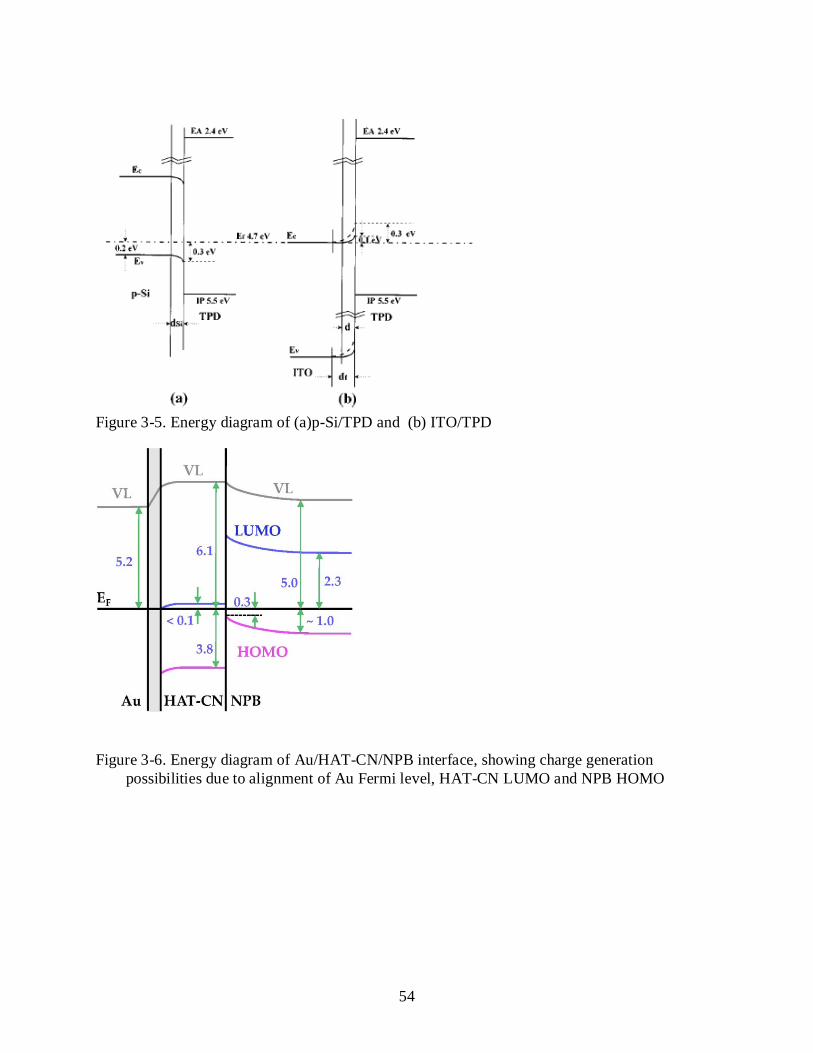
54
Figure 3-5. Energy diagram of (a)p-Si/TPD and (b) ITO/TPD
Figure 3-6. Energy diagram of Au/HAT-CN/NPB interface, showing charge generation possibilities due to alignment of Au Fermi level, HAT-CN LUMO and NPB HOMO

55
Figure 3-7. UPS studies of ITO/MoO3/NPB interface, showing shift in cut off position and the formation of a gap state within NPB
Figure 3-8. Energy level diagram of ITO/NPB and ITO/MoO3/NPB showing a reduced hole injection barrier and the location of the gap state.
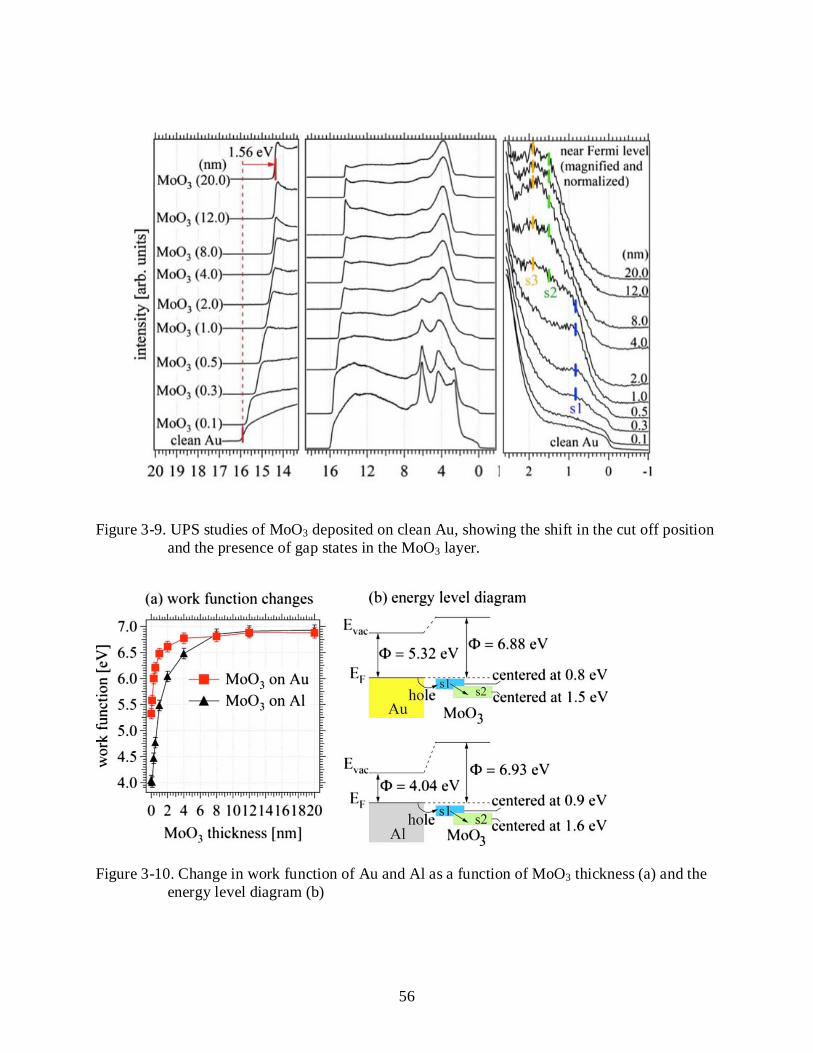
56
Figure 3-9. UPS studies of MoO3 deposited on clean Au, showing the shift in the cut off position
and the presence of gap states in the MoO3 layer.
Figure 3-10. Change in work function of Au and Al as a function of MoO3 thickness (a) and the
energy level diagram (b)

57
CHAPTER 4 EXPERIMENTAL METHODS
Introduction
This chapter covers actual process of fabrication and characterization of organic light
emitting diodes in the Organic Electronics Laboratory at the University of Florida. The initial
sections will cover the sample preparation methods along with a description of the tools and the
equipment. The device architecture, the materials and chemicals that were used and the
procedure for the fabrication are outlined. The next section talks about characterization of the
devices. There is a description of the testing setup and the standardized measurement techniques.
Device Preparation
Substrate Cleaning
ITO patterned glass substrates were purchased from Tinwell Technologies, Ltd. The
substrates measured 1 x 1 inch square and were sputter coated with 80nm of ITO with a reported
sheet resistance of ~40Ω/square. For the study of metal anodes, plain glass substrates were used,
but all subsequent steps are the same. These films are inherently rough, so the cleaning process
begins with mechanical rubbing with lint free cleaning wipes to clean and partly planarize the
surface. The glass substrates are then submerged in electronic grade Acetone purchased from
Fischer Scientific and subjected to ultrasonication for 15 minutes in a Branson 3510 sonicator.
This process is repeated for 15 minutes in laboratory grade 2-isopropyl alcohol. Ultrasonication
uses the principle of cavitation to ensure removal of dust, contaminants and organic films that
accumulate on the surface. The glass is then washed with de-ionized water to remove the solvent
and then dried using ultra high purity nitrogen.

58
Surface Treatment
Plain sputtered ITO has a work function of 4.3eV and is unsuitable for use as a hole
injection contact for most organic devices, so they must undergo surface treatment to modulate
their work function. The samples are therefore loaded into a UV-Ozone treatment unit, made by
the Jelight Company, Inc. Model 42, just prior to polymer deposition or thermal evaporation.
They are irradiated for a period of 15 minutes. During this treatment, the ITO films are
bombarded with high-energy oxygen ions that increase the oxygen concentration on the surface.
Due to this, ITO undergoes physical and chemical changes that in turn cause modification of
electronic properties.
Addition of Polymeric Hole-Injection Layer
In the case of the devices that utilized a polymeric hole injection layer like PEDOT:PSS,
the polymer is spin coated onto the cleaned and treated ITO substrates. The polymer plays the
dual role of acting as a hole injection layer as well as planarizing the ITO surface. The latter role
is crucial in the subsequent thermal evaporation of small molecules and metals on the surface.
The planarization removes the inhomogeneities of the ITO surface, allowing uniform deposition.
Its thickness also prevents the penetration of the hot cathode metal through to the anode and
thereby also reduces the occurrence of electrical shorts. The polymer is spin coated using a
Speciality Coating systems coater Model number KW-4A. About 0.5 mL of the polymer is cast
onto the stationary substrate through a 0.22 μm PVDF filter and a micropipette in order to
remove impurities and restrict the size of the polymer chains that are deposited. The spin rates
are ramped and set to control the thickness of the films. The excess solvent and polymer are
removed by centrifugal force. The samples are then baked in on a hot plate for 15 minutes at
1800C to remove all traces of the solvent and to anneal and harden the film. Other polymer films

59
will require a different spin coating speed as their viscosities are different and the baking times
will also vary, based on the composition of the preparation.
Thermal Evaporation
Thermal evaporation of small molecules, oxides and metals is carried out inside a vacuum
chamber. The materials are patterned using a set of stainless steel shadow masks that are placed
in close contact with the substrates. The anode mask corresponds to the ITO patterning on the
glass and was used only for the metal anodes. The overlap of the anode and cathode masks
creates four usable devices per substrate, each having an effective device area of 0.4cm2. The
chamber is pumped down to a pressure of 10-6 Torr using a cryogenic pump, backed by oil sealed
roughing pump. The materials are placed in evaporation boats that are radially arranged at the
base of the evaporator, and the substrates are suspended above them in a face-down manner in a
substrate holder. The materials and the substrates are separated by means of a movable shutter
that allows deposition of the material only under specified conditions. The materials are placed
in tungsten or boron nitride boats and connected between two posts to create an electrical
connection. High electrical currents passing through the boats cause the materials to heat and
evaporate. The evaporation rate is controlled by a quartz oscillator and a feedback circuit, and
the thickness correlations were tooled in using a profilometer. Due to the number of materials
involved and the non-rotational nature of this particular evaporator, not all substrates are in the
direct plume of the evaporated materials, so there is always minor variation in the thicknesses.
Upon completion of the evaporation, the chamber is backfilled with 1atm of nitrogen before the
samples can be removed and transferred to the glove box for encapsulation.
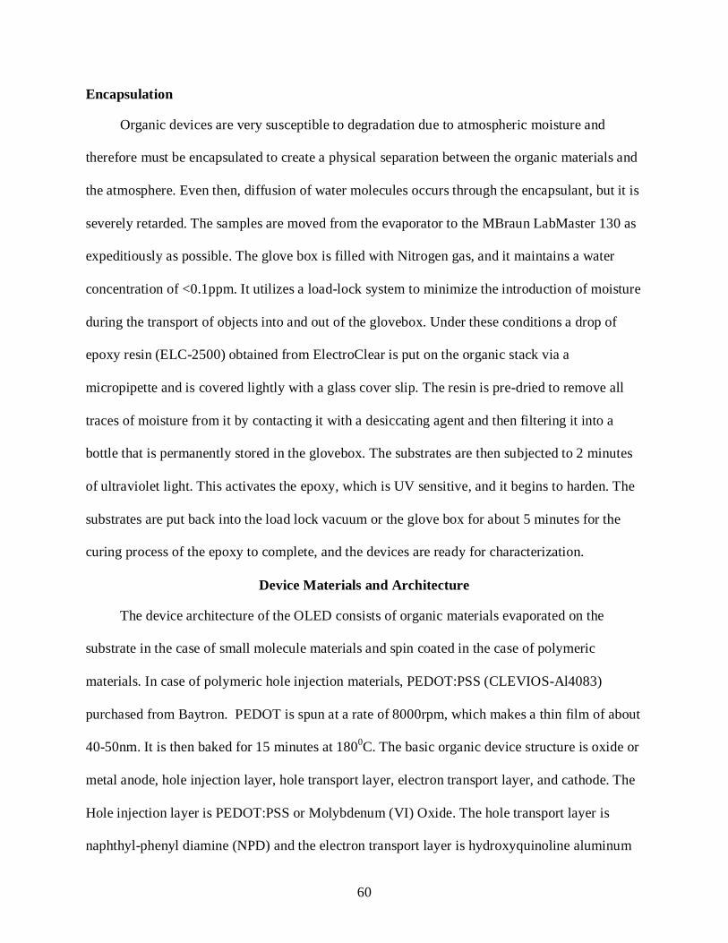
60
Encapsulation
Organic devices are very susceptible to degradation due to atmospheric moisture and
therefore must be encapsulated to create a physical separation between the organic materials and
the atmosphere. Even then, diffusion of water molecules occurs through the encapsulant, but it is
severely retarded. The samples are moved from the evaporator to the MBraun LabMaster 130 as
expeditiously as possible. The glove box is filled with Nitrogen gas, and it maintains a water
concentration of <0.1ppm. It utilizes a load-lock system to minimize the introduction of moisture
during the transport of objects into and out of the glovebox. Under these conditions a drop of
epoxy resin (ELC-2500) obtained from ElectroClear is put on the organic stack via a
micropipette and is covered lightly with a glass cover slip. The resin is pre-dried to remove all
traces of moisture from it by contacting it with a desiccating agent and then filtering it into a
bottle that is permanently stored in the glovebox. The substrates are then subjected to 2 minutes
of ultraviolet light. This activates the epoxy, which is UV sensitive, and it begins to harden. The
substrates are put back into the load lock vacuum or the glove box for about 5 minutes for the
curing process of the epoxy to complete, and the devices are ready for characterization.
Device Materials and Architecture
The device architecture of the OLED consists of organic materials evaporated on the
substrate in the case of small molecule materials and spin coated in the case of polymeric
materials. In case of polymeric hole injection materials, PEDOT:PSS (CLEVIOS-Al4083)
purchased from Baytron. PEDOT is spun at a rate of 8000rpm, which makes a thin film of about
40-50nm. It is then baked for 15 minutes at 1800C. The basic organic device structure is oxide or
metal anode, hole injection layer, hole transport layer, electron transport layer, and cathode. The
Hole injection layer is PEDOT:PSS or Molybdenum (VI) Oxide. The hole transport layer is
naphthyl-phenyl diamine (NPD) and the electron transport layer is hydroxyquinoline aluminum

61
(Alq3). The cathode consists of a thin layer of lithium fluoride covered by aluminum. The
specifications are shown in Table 4-1.
All metal anode materials were deposited at 0.5A/s, MoO3 was deposited at 0.5A/s, NPB
and Alq3 were deposited at 2A/s, LiF at 0.01A/s and the aluminum cathode at 2A/s. The different
anode materials were ITO or metal anodes. The metal specifications are shown in Table 4-2. In
the case of the metal anodes, the metal was covered with a 5nm thick layer of MoO3, which
along with the metal formed a composite anode. The MoO3 doubles as a hole-injection layer.
The structures of the organic materials are shown in Table 4-3.
Characterization Techniques
LIV Measurements
Current Voltage-Luminance measurements form the basis of the analysis of the feasibility
of metal anodes. Current Voltage (I-V) data was collected using a two probe technique to
determine the response of the device to electrical bias, using a Keithley Series 2400 sourcemeter.
Probes are connected such that the diode is run in the forward bias. The voltage is swept in the
positive direction, from 0V to 8V with a step of 100mV and a 0.001s source delay. The
compliance of the sourcemeter was set at 100mA. The luminance was measured by a silicon
photodiode, connected to a Keithley Series 6485 picoammeter to measure the response
photocurrent. The photodiode is calibrated using a luminance meter. The sourcemeter and the
picoammeter are controlled via GBIP interface and a computer using an in-house developed
LabView program.
Sample Holder
The sample holder used in the characterization is a custom device holder, as shown in the
figures and pictures. It consists of a plastic receptacle, in which gold pins are embedded. The
pins are connected internally to corresponding pins on the external side of the holder, which are
62
connected to the sourcemeter via alligator clips. The substrate is placed face down in the holder,
so that the electrodes come in contact with the pins. There is a spring-loaded cover on the holder
that ensures that the glass substrate is firmly pressed down onto the pins. This way, the
aluminum cathode ends up on the bottom and the semitransparent anode faces up. This
configuration is ideal for bottom emitting diodes. The silicon diode is positioned above the
center of the substrate, so that it receives only the perpendicularly emitting light waves. The
photodiode, the substrate holder and the substrate are housed in a closed black box to optically
isolate the system from the surrounding ambient light.
Analysis of Spectrum
The color spectrum of the light emitted from the diodes was measured via a spectrometer
manufactured by Ocean Optics, Inc. It consists a dedicated photodiode connected via a 200-
micron optical fibre. The photodiode is calibrated via a white light simulator to get a bright and
dark spectrum. Then the corrected spectrum is collected under similar conditions of optical
isolation. The data is analyzed using the SpectraScan software, by Ocean Optics, Inc. The
spectrum obtained is cropped to the visible region, as that is the only region of interest, and is
then normalized to the maximum value.
Capacitance Voltage Measurements
Capacitance-Voltage measurements were made to analyze the degradation of the organic
devices under electrical stressing. The capacitance was measured using a probe station,
connected to a Agilent 4282A precision LCR meter. The LCR meter is first calibrated by doing a
scan with the two probes not touching anything to calculate an open signal correction, and then
the two probes are kept in direct contact to get a short signal correction. The probes are
connected to the LCR meter using a 1m cable. The capacitance was measured in both the series
and the parallel mode. The d.c signal was swept from -2V to 5V with a step of 0.01V in the

63
forward direction. It is swept from the negative in order to avoid charging effects before the
measurement. The a.c. signal is set at 100mV and 200 Hz. The LCR meter was controlled via an
in-house developed LabView program.
Experimental Procedure
Thickness Variation of the Molybdenum Oxide Hole Injection Layer
The OLED devices were made with the architecture as described above, and the thickness
of the MoO3 layer was varied from 0nm, that is, direct contact of NPB onto the ITO substrate, to
5nm thick layer of MoO3. The devices were tested for current-voltage characteristics. The
experiments were repeated to ensure reliability, and representative devices are presented in the
next section.
Study of Metallic Anodes
In the development of metallic anodes, the substrates were cleaned as described and loaded
into the evaporator. 5nm of the respective metals were deposited using an anode pattern. The
MoO3 and the subsequent organic layers were all deposited using the organic mask and the
aluminum cathode was deposited using a cathode pattern. This layer of MoO3 forms a composite
anode with the metal and doubles as a hole injection layer. In the case of silver, a layer of MoO3
was deposited in the anode pattern below the silver metal to improve adhesion to the glass and
reduce the diffusion of silver into the organic stack. The lower layer of MoO3 also might play a
role in increasing the transmittance of the metal anode by improving the index matching of the
anode and the glass.
Lifetime Measurement of OLEDs
For the lifetime measurement of the OLEDs, the devices were fabricated as described
above and encapsulated in the glovebox. After the L-I-V and C-V measurement of the devices

64
under pristine conditions, they were returned to the glovebox. In the glove box they were
connected into an electrical circuit via alligator clips, and attached to the glass window of the
glovebox using vacuum tape, such that the light emitted could be measured from outside the
glovebox. The electrical circuit consisted of a constant voltage source and a 100ohm resistor in
series with the diode. The voltage read across the resistor was converted to current density
passing through the circuit knowing the resistance of the resistor, and the applied voltage was
read off the constant voltage source. The devices were run at a constant current density of
20mA/cm2. As the device degrades, the voltage required to maintain that current density
increases. The current density was monitored via the voltage across the resistor, and the voltage
at the source was accordingly increased. The luminance of the devices was measured using a
luminance meter. The glass does absorb some of the light and hence the readings from the
luminance meter and the calibrated photodiode do not match But as the luminance for the
lifetime study was always measured through the glass, the absorbance by the glass is constant,
and the comparison of the relative output of light for all the devices at all measurement points
still remains valid. At periodic intervals, the devices were removed from the glovebox for the
measurement of capacitance. The encapsulation ensured that the device did not degrade due to
the atmospheric moisture in the short periods that the samples were not in the moisture free glove
box environment. Due to the frequent application and removal of the alligator clips, the
electrodes tend to get scraped off, and therefore a contact blob of silver paste was put down on
the electrodes before the start of the experiment, and was found to be effective and intact till the
end of the study.

65
Table 4-1. Specification of Organic materials and films Compound Thickness Manufacturer Material Code Specifications MoO3 5nm Sigma Aldrich CAS 1313-27-5 99.99% metal
basis NPB 75nm Luminescent
Technology Corporation.
LT-E101 -
Alq3 50nm Luminescent Technology Corporation.
LT-401 -
LiF 1nm Sigma Aldrich CAS 7789-24-4 <5 microns, 99.98+%
Al 100nm Sigma Aldrich CAS 7429-90-5 5-15mm, 99.9% metal basis
Table 4-2. Specifications of Metals and films Compound Thickness Manufacturer Material Code Specifications Al 10nm Sigma Aldrich CAS 7429-90-5 5-15mm, 99.9%
metal basis Au 10nm Sigma Aldrich CAS 7440-57-5 1-6mm,
99.999% metal basis
Ag 10nm Sigma Aldrich CAS 7440-22-4 99.9999% metal basis
Table 4-3. Structures of Organic Compounds Name PEDOT:PSS NPB Alq3 MoO3 Structure

66
Figure 4-1. Schematic representation of device architecture

67
Figure 4-2. Thermal Evaporation Set up

68
Figure 4-3. L-I-V measurement setup
Figure 4-4. Diagrammatic Representation of L-I-V Setup
G

69
Figure 4-5. Sample Holder with 4 OLEDs (seen with the blue color)
Figure 4-6. Sample holder with one metal anode-OLED illuminated

70
CHAPTER 5 RESULTS AND DISCUSSION
Molybdenum Oxide as a Hole-Injection Material For Green OLEDs
Background
It is seen from the discussion on the theory of electroluminescence that the efficiency of
organic light emitting diodes is largely dependent on the charge injection and charge balance of
the holes and electrons into the organic material. In the course of research into efficient charge
injectors, Molybdenum Oxide has begun to receive some attention in the last few years. It is a
wide-gap material that behaves as an electron acceptor that is frequently used on the cathode
side, and as a connecting interlayer for tandem OLEDs. Its use as an efficient hole-injection
material has only recently begun to be investigated. The purpose of this study was to verify the
applicability of MoO3 as an efficient hole injection layer, and try to understand the reason behind
the enhancement of hole injection
Results
OLEDs were originally fabricated with and without a 5nm MoO3 buffer layer, and the
electrical and luminescent characteristics were observed. Once the benefits of MoO3 were
established, an intermediate thickness of 1nm MoO3 was used, so as to generate a gradation of
the thickness of the buffer layer. The Current-Voltage Characteristics are shown in Graph 5-1.
An increase in the current density was seen right from 0V upon the introduction of the 5nm
MoO3 layer, which is clearly illustrated from the semi-log plot. However, changing the
thickness to 1nm increases the current density even more, reaching the compliance of 100mA
before 8V. This is seen as the sudden flattening out of the I-V curve at around 7.5V. The 1nm
buffer layer OLED shows higher currents even before the turn-on voltage of around 2.2V. If the
flattening is ignored and the curve is extrapolated, then it is seen that the introduction of a 1nm

71
buffer layer increases the current density by about one decade at 8V, and a 5nm layer shows
about half a decade improvement. The luminescent response of the OLEDs is shown in Graph 5-
2. Similar enhancement of the light emission is seen for the MoO3 buffer layers, with the
compliance cut-off of the current leading to corresponding flattening of the luminance curve too.
The current efficiency plots are shown in Graph 5-3. The OLEDs with 5nm of the buffer layer
show an efficiency of 4cd/A, which is nominally greater than the OLEDs without a buffer layer.
The OLEDs with a buffer layer of 1nm show a current efficiency of 3cd/A. but over a much
larger range of current densities.
Discussion
From this set of experiments, the benefits of a MoO3 buffer layer are obvious. Addition of
even a single nanometer of MoO3 increases the current injection. Various studies on the effects
of MoO3 have also noted that there is usually a dramatic increase of current injection and
transport characteristics of organic devices when MoO3 is used as an interlayer or a hole-
injection layer. In terms of just carrier injection, it seems that a thinner layer of the buffer layer is
preferred. Studies on MoO3 interlayers has demonstrated that the introduction of 1nm of MoO3
shows the greatest enhancement over no MoO3 buffer layer, with the relative effect of MoO3
dropping off as the thickness of the buffer layer is increased. This effect is also seen in this study.
In another study in which the MoO3 buffer layer was sputtered rather than thermally evaporated,
the results indicate that a 0.75nm thick layer is optimum. Oxides are typically insulating
materials, with low carrier mobility. From this study, we can conclude that the enhancement
effect of MoO3 is more of an interface effect rather than a bulk effect, and therefore a thinner
layer minimizes any retardation of the carriers in the bulk. In the absence of dopants within the
hole transporting material NPB, the luminance of OLEDs is based on the recombination of holes
and electrons. Since OLEDs of this structure are believed to be hole dominated, and therefore

72
already in possession of an excess of holes, the observed increase in luminance is an interesting
phenomenon. In NPB/Alq3 type OLEDs, there have been numerous reports of hole build up near
the recombination interface, with the luminance being limited by the electrons reaching the
interface. With MoO3 enhancing the injection of holes, an internal electric field might be set up
within the organic stack to augment the existing external field, and promote the extraction of
electrons from the LiF/Al electrode. The increased density of electrons might explain the
increased luminance of OLEDs with buffer layers. The current efficiency plots on first glance
might seem to be contradictory to the rest of the data, with the efficiency of the 1nm buffer layer
having an efficiency worse than the OLEDs with 5nm buffer and even no buffer layer. This is
simply an effect of the definition of efficiency, being the ratio of the luminance over current
density. In OLEDs with MoO3 buffer layer, there is an increase in the current density and a
corresponding increase in luminance, probably due to the reason outlined above. However, the
improvement in luminance does not seem to be commensurate with the hole injection
enhancement. For the magnitude of increase of current density in 1nm MoO3 OLEDs, there has
not been an appropriate increase in magnitude of luminance. Therefore, even though the 1nm and
5nm buffer OLEDs show enhanced luminance, the increase in luminance is low relative to the
increase in current density and therefore by definition of efficiency, the 1nm buffer OLED shows
lower efficiency and the 5nm shows efficiency comparable to no buffer layer OLEDs. It should
therefore be noted that in this case, the lower efficiency is in no way attenuating the capability of
MoO3 to inject holes, with the current density curves providing a much better measure.

73
Metal-Based Composite Anodes
Background
Indium Tin Oxide (ITO) is currently the industry standard anode material. It possesses the
advantages of being a transparent conducting oxide having low sheet resistance and low optical
absorbance. This makes it potentially very viable as an anode for bottom emitting devices.
However, ITO has a comparatively low work function as compared to the HOMO of most
organic materials, even after the extensively used surface modification techniques like plasma
and UV-Ozone treatment. This difference presents a relatively large injection barrier for holes.
Moreover, ITO also makes a poor contact with organic materials, forming only a partially ohmic
contact with NPB. In order to reduce the hole-injection barrier as well as to improve the contact
between the anode and the organic semiconductor, various buffer materials are introduced
between the anode and the hole transporting materials. Materials like PEDOT:PSS notably
reduce the injection barrier by presenting an effective work function intermediate to the anode
and the organic solid, and make an almost ohmic contact with NPB by planarizing the anode.
With the success of MoO3 as a buffer layer than can be thermally evaporated, we investigated the
possibility of replacing ITO with metallic anodes, in an effort to displace the commercial
dependence on a rapidly diminishing supply of Indium based electrodes.
Results
In a series of experiments, we made green emitting OLEDs using ITO as anode, and then
replaced the ITO electrode with thermally evaporated metals, while keeping the remaining
architecture of the OLEDs the same. The first series of devices were made without a MoO3
buffer layer. The ITO-based OLEDs showed electroluminescence, indicating the injection of
both carriers without the presence of a buffer layer. On the other hand, the metal anode OLEDs
did not show any luminescent response, and the current-voltage curves show negligible currents

74
even at 8V. The open circuit response of these OLEDs showed that a buffer layer of MoO3 is
required for the realization of metal anode OLEDs, and all subsequent OLEDs were fabricated
with a 5nm buffer layer. This thickness might not be optimum, but it provides efficiency values
comparable to not having a buffer layer even though carrier injection is enhanced, as shown in
the previous data. Three metals having very different work functions were chosen. The current-
voltage plots are shown in Graph 5-4. It is observed that OLEDs with all the different anodes
show the same shape of the J-V curve. All the anodes show the same turn-on voltage of around
2.25V. Though there is a variation in the characteristics before turn-on, the characteristics are
remarkably similar after turn-on, with the variation being less than half a decade at 8V. The
luminescent responses are shown in Graph 5-5. The shape of the curves is again similar, with
very low variation in the luminescent output for the different anodic materials. It is interesting to
note that the materials showing a relatively higher current density are not the same as those
showing higher luminance. The current efficiencies were calculated and are shown in Graph 5-6.
The ITO OLEDs are comparable to the previously made OLEDs. Though the OLEDs with Gold
anodes have lower efficiency than ITO OLEDs, it is within the acceptable range for this species
of OLED. The aluminum OLEDs are slightly lower than expected, but the silver anodes are
actually better than ITO OLEDs at least on the basis of current efficiency, approaching 5 cd/A at
higher densities. The normalized spectra of the light emitted from OLEDs with the different
anodes are shown next in Graph 5-7. The OLEDs do not emit at any other wavelength, so the
spectrum can be cropped to the visible region. All the emissions are peaked at about the same
wavelength, and the spectral curves are similarly shaped. The Aluminum spectrum matches the
ITO spectrum exactly, while the Gold and the Silver spectra are very similar. Both the latter are

75
slightly red-shifted, and show emission over a slightly broader range, rather than having a sharp
peak in the intensity.
Discussion
The reported values of the work functions of Aluminum, Silver and Gold are 4.28, 4.26
and 5.3 respectively. ITO has a work function ranging from 4.5 – 5eV after surface treatment.
The conductivities of Aluminum, Silver and Gold are 37.8, 63.01 and 45.2 (x106 S/m).
Aluminum anode OLEDs without a MoO3 buffer layer do not show any electroluminescent
response within the range of testing. However they do show weak luminance at approximately
15V. As a comparison, ITO based OLEDs show luminance at around 2.2 – 2.5 V. This implies
that the injection barrier for an aluminum anode without the presence of MoO3 is very large, but
under sufficient external bias, it will inject electrons. But from Graph 5-4, the presence of MoO3
brings down the turn-on voltage to around 2V. From this we can conclude that the MoO3 buffer
layer reduces the injection barrier. However Gold anode OLEDs without the buffer layer also do
not show electroluminescence. This implies that although Gold and ITO have comparable work
functions, gold anodes are poor injectors. In that case MoO3 probably forms a composite anode
with the metal and thereby improves injection. It is therefore very significant that the current
voltage characteristics of all the different anodes align so well. The fact that they all have the
same turn-on voltage implies that the effective injection barrier is either the same or very similar.
The fact that there is no injection barrier at the metal/MoO3 interface, though the work function
difference between Aluminum and Moo3 is large, also points towards the formation of a
composite anode. The Luminance voltage curves also mirror these observations. Since
luminance depends on recombination of holes and electrons, similar luminance curves imply that
holes are being injected from MoO3 into NPB at the same efficiency. So MoO3 itself is
maintaining its bulk properties and its interactions with NPB, and therefore the effect is

76
interfacial in nature and is seen only at the metal /MoO3 interface. Another very interesting
outcome from analysis of the luminance curves is that all metal anode OLEDs display
comparable or higher luminance than ITO OLEDs. This should not have been the case, since the
OLED architecture is bottom emitting, and all the metal anodes have lower transmission
coefficients than ITO. When combined with the spectral results, the cause of this discrepancy can
be explained via the formation of a metal cavity. When the unbiased OLED pixels are visually
observed, the ITO OLEDs have a gray color due to the underlying metal cathode, but the metal
anodes OLEDs have an almost opaque violet color that underwent a red shift when the overall
thickness of the stack was increased. The existence of a metal cavity would mean that there will
be internal reflection of light, and the emitted light will be collimated due to constructive
interference within the cavity. This means the will be less destructive interference and
divergence after the light leaves the device, and consequently, more light reaches the detector.
The metal cavity promotes a non-Lambertian distribution of the emission intensified along the
normal direction, which also translates to increased photo-detection. Another effect of the metal
cavity can be seen in the emission spectra. The ITO OLED and the Aluminum OLED which
shows only a very weak cavity effect shows a peak in the spectrum at 512nm, but the Silver and
Gold anode show a red shift as well as a broadening of the maximum intensity to show a range
525nm to 550nm, rather than a peak. This effect is contrary to the conventional metal cavity
effect that shows a narrowing of the emission spectrum instead. Silver has the highest reflectivity
of all metals, and therefore forms the best mirror for the metal cavity, and this is seen in the
luminance plots, where the luminance of Silver anode OLEDs is comparatively higher. The
higher reflectivity and conductivity of Silver do contribute to the slight differences in Luminance
and current data, and the efficiencies are therefore understandably higher.

77
It should be pointed out that the efficiency calculations for this set of experiments could be
misleading for two reasons. First, the effect of the metal cavity is as described above. Due to this,
the luminance that is measured for the Silver and Gold OLEDs cannot be compared to the
luminance of the ITO OLED that lacks the metal cavity enhancement. This is an optical effect
and has no real bearing on the physics of the metal anodes being studied. Therefore to equate
these quantities, we can qualitatively assume that the luminance of the Silver and Gold OLEDs is
in fact lower, which would mean that their efficiencies have been overestimated. On the other
hand, the absorption and transmission of the metal anodes is not accounted for, and as the ITO
anode is substantially more transparent, the luminescent emission from all the metal anode
OLEDs might be damped by the translucence of the anodes, again causing misrepresentation of
the efficiency. Therefore, the efficiencies of the metal anodes should not be directly compared to
ITO OLEDs.
Another important consideration in this study is the quality of the metal anodes. The ITO
anodes are commercially sputtered to a thickness of 80nm, and therefore are sufficiently thick
and uniform. The thickness of the metal anodes was deliberately kept low to improve the
transmittance and so they were only 10nm thick, and were thermally evaporated onto glass
substrates. The effect of minor thickness variation would be much more pronounced. It is
therefore reasonable to assume that the contact between the metal and subsequently deposited
materials would be worse than the ITO anodes. The second concern is that since the metal
anodes were so thin, the current would be passing through a much smaller cross section. The
metal anode OLEDs were therefore subjected to a higher cross sectional current density in order
to compare them to ITO OLEDs. However, due to this, the effect of joule heating would be
significantly more pronounced, and the metal anode OLEDs were also expected to degrade

78
faster, and indeed degradation could be seen in current characteristics after a single sweep in
some cases.
Lifetime and Degradation of OLEDs Based on the Performance of Hole-Injection Materials
Background
Apart from efficiency, the operating lifetime of OLEDs is the other obstacle to its
commercial application, and there have been concerted effort to understand the nature of the
degradation of OLEDs. Sometimes a compromise must be made between efficiency and lifetime,
as in the case of hole transporting materials. OLEDs made using TPD, a material with a lower
glass transition temperature, which translates to faster crystallization usually have lower lifetime,
yet typically show higher efficiencies. The case for NPB is the exact opposite. In another
landmark paper by Kondakov et al., [96] degradation has been attributed to the build-up of holes
at the NPB/Alq3 interface. By extension of this, there should be a build up of holes at the
anode/hole transport material interface too. By varying the hole-injection material, we can vary
the effective barrier for hole-injection and therefore vary the concentration of holes at this
interface. This study provides a preliminary investigation of degradation at the
anode/semiconductor interface.
Results
In this study, we fabricated OLEDs using a number of commercial and proprietary hole-
injection materials. Among these were PEDOT:PSS, polythienothiophene (PTT) doped with
poly(perfluoroethylene-perfluoroethersulfonic acid) (PTT:PFFSA) [71], MoO3 and CuPc. We
made a comparison of OLEDs using polymeric hole-injection materials. The architecture was a
little different, with the NPB and Alq3 layers being 40nm and 50nm respectively. The polymers
were spin coated using recipes optimized for them individually, and the resulting annealed layers
were around 70nm thick. Graph 5-8 shows the current voltage curves for them, and an OLED

79
using 5nm MoO3 as a buffer layer is included for comparison. The plot also shows the
luminescent response, and it is seen that the luminance is roughly proportional to the current
density. It can also be seen that the current densities and the luminance of all the OLEDs is very
similar, and the turn on voltage for all devices is the same. The current efficiencies are shown in
Graph 5-9, and again they are remarkably similar. The MoO3 OLED does show a higher
efficiency in spite of lower current density and luminance values. For the purpose of lifetime
comparison, an OLED was fabricated without a hole-injection layer, and was compared to the
OLEDs with polymeric buffer layers. The devices were operated continuously at 20mA/cm2 and
the measurement study was conducted as outlined in the experimental section. The normalized
luminescent decay is shown in Graph 5-10, and the voltage rise data is summarized in Graph 5-
11. It is obvious that the lifetime of devices with similar performance is quite different. The
Baytron PEDOT:PSS (CH8000) reaches half life (50% luminance) in less 20 hours, the OLED
without a buffer layer degrades 45% and PTT:PFFSA -2 degrades 10% after more than 120
hours. We also compared the degradation of OLEDs without a buffer layer and
polythienothiophene (PTT) doped with poly(perfluoroethylene-perfluoroethersulfonic acid)
(PTT:PFFSA-2), using C-V analysis. These two devices represent the largest and smallest
effective hole-injection barrier respectively. The C-V data is presented in Graph 5-12. The
important characteristic is the turn-on voltage, and we can see that it shifts to the right over the
course of the degradation, although the rate of the shift is significantly slower for PTT:PFFSA-2
OLEDs than for OLEDs without a buffer layer.
Discussion
The operating lifetime has so far been linked mainly to the degradation of the organic
materials. A very common hole transporting material TPD has a lower glass transition
temperature as compared to NPB, which leads to more rapid crystallization. Therefore the higher

80
efficiency of TPD OLEDs is compromised by its shorter lifetime. In Kondakov’s paper, [97] the
chemical degradation of NPB is due to the presence of excitons formed after the recombination
of holes and electrons at the interface of NPB/Alq3, which leads to fragmentation of the NPB
molecule progressively away from the interface. This leads to the decay of luminance over time.
In our experiment, the OLED structure for all devices is the same apart from the hole-injection
layer, and yet we see a difference in lifetime. Based on this, we can say a priori that there is also
some change occurring near the anode/semiconductor interface. The primary difference between
these materials is their work function, thereby presenting a different effective injection barrier. In
1995, in their work on different hole transporting materials, Adachi et al. suggested that the hole-
injection barrier causes joule heating near the anode interface, which causes local crystallization
of the material, and subsequent degradation [98]. The correlation of the hole-injection barrier and
the rate of degradation does in part confirm this model. But it contradicts the very convincing
argument put forth by Kondakov, that states both holes and electrons are required to initiate
degradation.
It was also observed by Scott et al. that oxygen diffuses out of ITO into a polymeric
OLED, causing it to fragment, reduce carrier mobility and quench luminescence [99]. UV-Ozone
treatment is a common method to increase the work function of ITO, by which the surface of
ITO is enriched by oxygen atoms. It has been observed the work function of treated ITO will
reduce if the anode is left in atmosphere, indicating that the adsorbed oxygen is being released.
Under electrical stress, it is possible that oxygen is released from the anode and diffuses into the
organic material. This would have a combined effect of degrading the organic material as well as
lowering the work function of ITO, which would explain the loss in luminance and rise in
driving voltage. It has also been observed that Indium diffuses out of ITO into PEDOT:PSS,

81
particularly during the spin coating process[100], to the same destructive effect. The different
hole-injection materials have different resistances to these diffusive elements and this may
contribute to the difference observed in their lifetimes.
The second evidence we present is analysis of degradation via C-V measurements in
Figure XII. Shrotriya et al. analyzed the C-V response of OLEDs [101], and have attributed the
turn on rise of capacitance as the onset of injection of holes, and the capacitance peak as the
point of carrier recombination. The shift of the capacitance “turn-on” voltage implies that more
voltage is required to inject holes. This increase in resistance to carrier injection could be due to
the chemical degradation of the materials or the change in the work function of the anodes.
Therefore if the anode/organic interface a location for degradation, this could affect the
interfacial dipole and therefore hamper charge injection. Based on the current understanding of
interfaces, it could be anything from modification of the characteristics of the interfacial dipoles
to the redistribution of the energies of the intermediate states associated with them. Without
further investigation, we cannot comment with any certainty about the mechanism of this
degradation. All we can conclude is that better hole-injection retards this particular cause of
degradation.

82
Figure 5-1. Current Density plots as a function of thickness of MoO3 layer
Figure 5-2. Luminance Plots as a function of thickness of the MoO3 layer
0 2 4 6 8
1
10
100
1000
10000
Lumi
nanc
e
Voltage
ITO ITO / Moly 1nm ITO / MoO3 5nm
0 2 4 6 81E-5
1E-4
1E-3
0.01
0.1
1
10
100
1000
Curre
nt D
ensit
y
Voltage
ITO ITO/MoO3 1nm ITO/ MoO3 5nm

83
Figure 5-3. Current Efficiency Plots as a function of MoO3 layer thickness
0 10 20 30 40 500
1
2
3
4
5
Curre
nt E
fficie
ncy
Current Density
ITO ITO/MoO3 1nm ITO / MoO3 5nm

84
Figure 5-4. Current Density plots of OLEDS with different anodes
Figure 5-5. Luminance plots of OLEDs with different anodes
0 2 4 6 8
1
10
100
1000
10000
Lum
inan
ce (c
d/m
2 )
Voltage (V)
ITO / MoO3 Al / MoO3 Au / MoO3 Ag / MoO3
0 2 4 6 81E-6
1E-5
1E-4
1E-3
0.01
0.1
1
10
100
1000
Curre
nt D
ensit
y (m
A/cm
2 )
Voltage (V)
ITO / MoO3 Al / MoO3 Au / MoO3 Ag / MoO3

85
Figure 5-6. Current Efficiency plots of OLEDs with different anodes
20 40 60 80 1001
2
3
4
5
Curre
nt E
fficie
ncy
(cd/
A)
Current Density (mA/cm2)
ITO / MoO3 Al / MoO3 Au / MoO3 Ag / MoO3

86
Figure 5-7. Emission Spectra of OLEDs with different anodes
350 400 450 500 550 600 650 700 750 800 850-0.2
0.0
0.2
0.4
0.6
0.8
1.0
Norm
alize
d In
tens
ity
Wavelength (nm)
ITO / MoO3 Al / MoO3 Au / MoO3 Ag / MoO3

87
Figure 5-8. Current Density and Luminance plots for OLEDs made with various polymeric hole injection materials. INSET: Luminance response of the OLEDs
0 2 4 6 8 101E-3
0.01
0.1
1
10
100
1000
APHIL98 APHIL136 PEDOT8000 PEDOT4083 MoO3 5nm
Curre
nt d
ensit
y [m
A/cm
2 ]
Voltage [V]
100
1000
10000
100000
Lum
inan
ce [c
d/m
2 ]

88
Figure 5-9. Current Efficiency plots of OLEDs with polymeric hole injection materials
0.1 1 10 100
1
2
3
4
5
APHIL98 APHIL136 PEDOT8000 PEDOT4083 MoO3 5nm
Curre
nt e
fficie
ncy
[cd/
A]
Current density [mA/cm2]

89
Figure 5-10. Lifetime Decay of luminance of OLEDs with different polymeric hole-injection
materials
Figure 5-11. Lifetime Voltage rise of OLEDs with different polymeric hole-injection materials
0 20 40 60 80 100 120 1400.1
0.2
0.3
0.4
0.5
0.6
0.7
0.8
0.9
1.0
1.1
Norm
alize
d Lu
min
ance
Time (hr)
No HIL PEDOT 8000 PEDOT 4083 AP HIL 98 Aphil 136
0 20 40 60 80 100 120 1401.00
1.05
1.10
1.15
1.20
1.25
1.30
1.35
1.40
1.45
1.50
Norm
alize
d Vo
ltage
Time (hr)
NO HIL PEDOT 8000 PEDOT 4083 APHIL 98 APHIL 136

90
-2 -1 0 1 26.00E-010
8.00E-010
1.00E-009
1.20E-009
1.40E-009
1.60E-009
1.80E-009
2.00E-009
2.20E-009
No HIL 00 hours 24 hours48 hours 72 hours 96 hours
Capa
citan
ce [F
]
Voltage [V]
Figure 5-12. Capacitance-Voltage Data of OLEDs under electrical stress:
-2.0 -1.5 -1.0 -0.5 0.0 0.5 1.0 1.5 2.0 2.51.50E-009
2.00E-009
2.50E-009
3.00E-009
3.50E-009
4.00E-009
4.50E-009
5.00E-009
Voltage [V]
Capa
citan
ce [F
]
00 hours 48 hours 72 hours 96 hours120 hours
APHIL136

91
CHAPTER 6 SUMMARY AND FUTURE WORK
Summary of Results
Green fluorescent OLEDs were fabricated with NPB and Alq3 as the hole transporting and
electron transporting materials respectively to study the nature of injection across a metal/organic
semiconductor interface. It was found that performance of MoO3 was comparable to
contemporary materials like CuPc and PEDOT:PSS, and they all have similar operating voltages
and efficiencies. MoO3 combines the advantages of high transparency and ohmic contact nature
of PEDOT:PSS and the ability to be thermally evaporated like CuPc.
The effect of the thickness of MoO3 on the electronic properties of OLEDs was examined,
and it was found that the presence of the buffer layer improves the performance of the device
significantly. There is a dramatic enhancement upon the introduction of a nanometer-thick layer
of MoO3, and the relative improvement drops off with increasing thickness. This implies that the
electron accepting MoO3 retards holes in its bulk and its entire efficacy lies in its role as an
interface modification agent.
ITO has a work function ranging from 4.5 – 5eV after surface treatment, whereas
Aluminum, Silver and Gold have work functions of 4.28, 4.26 and 5.1 respectively. The HOMO
level of NPB is 5.4eV. Yet in the presence of MoO3, OLEDs fabricated using all these materials
as anodes behave identically. Performance curves and the emission spectra are very similar if
you take into account the formation of the metal cavity. These results suggest that the presence
of MoO3 neutralizes the difference in the work functions of the anodes, and the only effective
work function is that of MoO3.
A comparative study of the lifetime of OLEDs was conducted using a number of
conducting polymers to inject holes. It was observed that the rate of degradation of the OLED is

92
retarded when the efficiency of the device is improved via better hole-injection characteristics.
This study concludes that at least an empirical relation exists between the performance, operating
lifetime and the injection barrier in organic devices.
Future Work
Despite being a strong electron acceptor, Molybdenum trioxide has been used extensively
has a hole-injection material in conjunction with ITO. This study shows that in the presence of
MoO3, any thin conducting metal may replace the ITO anode. This has great implications in
display technology, as ITO is the predominant transparent anode material. If we account for the
metal cavity effect, we conclude that the efficiency of the ITO-based OLEDS is significantly
better; nonetheless this study serves as a proof of concept, that with optimization, metal anodes
can be engineered to be a viable substitute for ITO. As a sample improvement, if the metal anode
were to be sputtered rather than thermally evaporated, the resulting metal film would be of
higher quality, as well as more transparent. It might be interesting to repeat this experiment,
using these films to see whether the result can be enhanced. Sputtering would also allow for a
thicker metal film to be used without compromising the transparency, and would avoid the
deleterious effects of joule heating.
The lifetime study of MoO3 based OLEDs is also worthwhile, because of the relation of
efficiency, lifetime and injection barrier. Currently, metal anode OLEDs are too unstable to
undergo any degree of prolonged electrical stressing and degrade after a few sweeps, but as the
methods of depositing metal anodes are improved, and the interaction between the metal and
oxide is better understood, this might be attempted.
Clearly, the catalyst of this study is the Molybdenum trioxide film. Yet, we have an
incomplete understating about the nature of the interfaces between MoO3 and ITO, MoO3 and
the metal, and MoO3 and the organic material. In recent findings, it has been shown that MoO3

93
accepts electrons from Indium from ITO to cause the In 3d peaks in an XPS spectrum to move to
a higher energy [79]. Gain of electrons by the MoO3 means it undergoes reduction. In this
context, it would mean that Mo6+ ions are being reduced to Mo4+ ions, which means
Molybdenum trioxide might now be Molybdenum dioxide. Indeed, studies have shown than
amorphous MoO3 does reduce to a crystalline MoO2 in the presence of hydrogen [102], which
could also be brought about by organic hydrocarbons as well as ITO. MoO2 is known to have a
higher conductivity than MoO3. The conversion of MoO3 to MoO2 is probably limited to a few
atomic layers, which helps explain why thinner films show higher current densities. XPS studies
of MoO3 films on Al, Au and Ag should show energy shift of a similar nature. Similarly,
deposition of an organic layer on MoO3 should show an energy shift in the energy of Mo peaks,
with Mo moving to a lower energy state. If this reduction is better understood, it may be possible
to manipulate it and thereby improve on the performance of current MoOx devices.
The shift of the work function of the metal with respect to that of MoO3 is also a crucial
piece of evidence for this work. To qualitatively study this, a photovoltaic measurement may be
conducted that would help to determine the open circuit voltage of the device. In this technique,
the photocurrents of the devices are measured under illumination by a simulated solar lamp. If all
the parameters are kept the same and the interface dipole effect is ignored, then the VOC reflects
the built in potential between the electrodes. A study previously conducted on MoO3 OLEDs
shows an increase on VOC as compared to an ITO OLED without the buffer layer. An increase in
VOC translates to a smaller hole injection barrier as the effective work function of the anode is
increased. If we make OLEDs with metal anodes and MoO3 and measure VOC, and see the same
built-in potential for all OLEDs, that would tell us something about the nature of the shift in
work function of the metal.

94
Similarly, UPS studies also tell us a great deal about the work function of the anode
structure, and can be used in conjunction to show that metals in the presence of MoO3 show the
same effective work function and therefore the same barrier to hole injection. There have been
studies conducted on the existence of gap states in MoO3 when deposited on metals and the
presence of gap states in NPB when deposited on MoO3. UPS studies of the complete system
conducted incrementally would help explain the nature of carrier injection
The lifetime study of OLEDs as a function of hole-injection barriers is very significant
from an economic point of view. Single carrier devices fabricated without Alq3 and a very high
work function metal like Au as cathode would eliminate the NPB/Alq3 interface. Charge
transport would then be in a single material and with a single metal/organic interface. The
voltage rise data and C-V data should show any change in driving voltage, a change indicating
deterioration of either the interface or the material itself. Change in work function or built in
potential combined with the voltage data would isolate the effect of this interface and provide
deeper insight into the nature of the degradation, since this is a simpler system as compared to a
bi-layer, dual carrier system. An informative study would be to electrically stress the devices and
compare the concentrations of Indium and oxygen in the polymer and in the NPB layer via XPS.
The work function changes of the anodes may be measured by conducting a Kelvin probe or a
temperature dependent study, which would non-invasively give the work function change as a
function of time of electrical stress. If diffusion of elements were indeed found to be the cause of
degradation, it may be possible to design a better and more resistant hole injection material and
processing method that retards anode etching that would significantly enhance its lifetime and
performance.

95
REFERENCES
1. A. Bernanose, M. Comte and P. Vouaux, J. Chem Phys. 50, 65 (1953)
2. M. Pope, H. Kallmann, and P. Magnate, J. Chem. Phys. 38, 2042 (1963)
3. M. Sano, M. Pope, and H. Kallmann, J. Chem. Phys. 43, 2920 (1965)
4. W. Helfrich and W.G. Schneider, J. Chem Phys. 14, 229 (1965)
5. W.G. Schneider and W. Helfrich, J. Chem. Phys 44, 2902 (1966)
6. G.G. Roberts, M.M. McGinnity, W.A. Barlow, and P.S. Vincett, Solid State Commun., 32, 683 (1979).
7. P.S. Vincett, W.A. Barlow, R.A. Hann, and G.G. Roberts, Thin Solid Films, 94, 171 (1982)
8. R.H. Partridge, Polymer, 24, 748, (1983)
9. S. Hayashi, H. Etoh, and S. Saito, Jpn. J. Appl. Phys. 25, L773 (1986)
10. C.W. Tang, and S.A. VanSlyke, Appl. Phys. Lett., 51, 913, (1987).
11. J.H. Burroughes, Nature, 347, 539 (1990).
12. G He, O Schneider, D Qin, X Zhou, M Pfeiffer, and K Leo, J. Appl. Phys. 95, 5773 (2004)
13. R.F. Service, Science, 310, 1762 (2005)
14. J Kido, H Hayase, K Honyawa, K Nagai, and K Okuyama, Appl.Phys.Lett., 65, 2124 (1994)
15. Y.Yang, Q.Pei, and A.J.Heeger, J.Appl.Phys. 79, 934 (1996)
16. J. Kido, H. Shionoga, and K. Nagai, Appl. Phys. Lett., 67, 2281(1995)
17. C-C Wu, C-Wei Chen, and T-Y Cho, Appl. Phys. Lett., 83, 611 (2003)
18. K.C. Kao, W. Hwang, Electrical Transport in Solids with Particular Reference to Organic Semiconductors, Pergamon Press, New York, 1981.
19. Z. Kafafi, “Organic Electroluminescence” CRC press, 2005
20. L. S. Hung, C. W. Tang, and M. G. Mason, Appl. Phys. Lett. 70, 152 (1997)
21. C.W. Tang, C.H. Chen, R. Goswami, US Patent 4,769,292 (1988).

96
22. S.A. VanSlyke, C.H. Chen, C.W. Tang, Appl. Phys. Lett. 69 (1996) 2160
23. Y. Shirota, Y. Kuwabara, H. Inada, Appl. Phys. Lett. 65, 807 (1994).
24. Y. Yang, A.J. Heeger, Appl. Phys. Lett. 64, 1245 (1994).
25. Y. Cao, G. Yu, C. Zhang, R. Menon, A.J. Heeger, Synth. Met. 87, 171 (1997)
26. A. Elschner, F. Bruder, H.-W. Heuer, F. Jonas, A. Karbach, S. Kirchmeyer, S. Thurm, R. Wehrmann, Synth. Met. 111, 139 (2000)
27. Y Hamada, T Sano, K Shibata, K Kuroki Jpn. J. Appl. Phys. 34 L824 (1995)
28. M Yoshida, A Fujii, Y Ohmori, and K Yoshino, Appl. Phys. Lett. 69, 734 (1996)
29. M.A. Baldo, ME Thompson, SR Forrest Pure Appl. Chem., 71, 11, 2095, (1999)
30. M.A. Baldo, M.E. Thompson, S.R. Forrest, Nature 403, 750 (2000)
31. C. B. Duke, L. B. Schein, Phys. Today 33, 42 (1980).
32. H Ishii, K Sugiyama, E Ito, K Seki, Adv Mater. 11,8, 605 (1999)
33. D. P. Woodruff, T.A. Delchar, Modern Techniques of Surface Science, Cambridge University Press, Cambridge (1986).
34. K. Wandelt, in Thin Metal Films and Gas Chemisorption (Ed: P. Wissmann), Elsevier, Amsterdam (1987).
35. N. Lang,W. Kohn, Phys. Rev. B 1, 4555 (1970).
36. N. D. Lang,W. Kohn, Phys. Rev. B, 3, 1215 (1971)
37. J. Hoelzel, F. K. Schulte, H. Wagner, Solid State Surface Physics, Springer, Berlin (1979).
38. C. Slater, N. H. Frank, Electromagnetism, McGraw-Hill, New York, (1947).
39. S. M. Sze, Physics of Semiconductor Devices, 2nd ed.,Wiley, New York (1981).
40. M. Schott, in Organic Conductors: Fundamentals and Applications (Ed: P. Farges), Marcel Dekker, New York (1994).
41. K. C. Kao, W. Hwang, Electrical Transport in Solids, Pergamon, Oxford (1981)
42. Y. Park, V. Choong, E. Ettedgui, Y. Gao, B. R. Hsieh, T. Wehrmeister, K. Muellen, Appl. Phys. Lett. 69, 1080 (1996).
43. A. Rajagopal, C. I. Wu, A. Kahn, J. Appl. Phys. 83, 2649. (1998)

97
44. K. Seki, Mol. Cryst. Liq. Cryst. 1989, 171, 255.
45. K. Seki, in Optical Techniques to Characterize Polymer Systems (Ed: H. Baessler), Elsevier, Amsterdam (1989)
46. S. Hüfner, Photoelectron Spectroscopy, 2nd ed., Springer, Berlin (1996).
47. A. Rajagopal, C. I. Wu, and A. Kahn J. Appl. Phys. 83, 2649 (1998)
48. I. D. Parker, J. Appl. Phys. 75, 1656 (1994).
49. Q. T. Le, L. Yan, Y. Gao, M. G. Mason, D. J. Giesen, and C. W. Tang, J. Appl. Phys. 87, 375 (2000).
50. M. G. Mason, C. W. Tang, L. S. Hung, P. Raychaudhuri, J. Madathil, D. J. Giesen, L. Yan, Q. T. Le, Y. Gao, S. Y. Lee, L. S. Liao, L. F. Cheng, W. R. Salaneck, D. A. d. Santos, J. L. Bredas J. Appl. Phys. 89, 2756 (2001)
51. L. S. Hung, C. W. Tang, and M. G. Mason, Appl. Phys. Lett. 70, 152 (1997)
52. T. M. Brown, R. H. Friend, I. S. Millard, D. J. Lacey, T. Butler, J. H. Burroughes, and F. Cacialli, J. Appl. Phys. 93, 6159 (2003)
53. L. S. Hung, C. W. Tang, M. G. Mason, P. Raychaudhuri, and J. Madathil,Appl. Phys. Lett. 78, 544 (2001)
54. S. E. Shaheen, G. E. Jabbour, M. M. Morrell, Y. Kawabe, B. Kippelen, N. Peyghambarian, M. F. Nabor, R. Schlaf, E. A. Mash, and N. R. Armstrong,J. Appl. Phys. 84, 2324 (1998)
55. T. M. Brown, R. H. Friend, I. S. Millard, D. J. Lacey, J. H. Burroughes, and F. Cacialli, Appl. Phys. Lett. 79, 174 (2001)
56. H. Kim, C. M. Gilmore, A. Pique, J. S. Horwitz, H. Mattoussi, H. Murata, Z. H. Kafafi, and D. B. Chrisey, J. Appl. Phys. 86, 6451 (1999)
57. T. Maruyama and K. Fukui, Thin Solid Films 203, 297 (1991)
58. W.-F. Wu, B.-S. Chiou, and S.-T. Hsieh, Semicond. Sci. Technol. 9, 1242 (1994)
59. P. Nath, R. F. Bunshah, B. M. Basol, and O. M. Staffsud, Thin Solid Films 72, 463 (1980)
60. V. Vasu and A. Subrahmanyam, Thin Solid Films 193/194, 696 (1990)
61. J. P. Zheng and H. S. Kwok, Appl. Phys. Lett. 63, 1 (1993)
62. F. Li, H. Tang, J. Shinar, O. Resto, and S. Z. Weisz, Appl. Phys. Lett. 70,2741 (1997)
98
63. C. C. Wu, C. I. Wu, J. C. Strum, and A. Kahn, Appl. Phys. Lett. 70, 1348 (1997)
64. I.M. Chan, W. C. Cheng, and F. C. Hong, Appl. Phys. Lett. 80, 13 (2002).
65. S. K. So, W. K. Choi, C. H. Cheng, L. M. Leung, and C. F. Wong, Appl. Phys. A 68, 447 (1999)
66. S. F. J. Appleyard and M. R. Willis, Opt. Mater. 9, 120 (1998)
67. E. W. Forsythe, M. A. Abkowitz, Yongli Gao, and C. W. Tang, J. Vac. Sci. Technol. A 18, 1869 (2000)
68. S. M. Tadayyon, H. M. Grandin, K. Griffiths, P. R. Norton, H. Aziz and Z. D. Popovic, Org Elect, Vol 5, Iss 4,157 (2004)
69. S. C. Tse, S. W. Tsang, and S. K. So, J. Appl. Phys. 100, 063708 (2006)
70. G. G. Malliaras and J. C. Scott, J. Appl. Phys. 85, 7246 (1999)
71. K.R. Choudhury, J. Lee, N. Chopra, A. Gupta, X. Jiang, F. Amy, F. So, Adv Func. Mat. 19, 3, 491 (2009)
72. I-Min Chan, Tsung-Yi Hsu, and Franklin C. Hong, Appl. Phys. Lett. 81, 1899 (2002)
73. J Li, M Yahiro, K Ishida, H Yamada, K Matsushige - Synthetic Metals, 151,2,141 (2005)
74. J. X. Tang, Y. Q. Li, L. R. Zheng, and L. S. Hung, J. Appl. Phys. 95, 4397 (2004)
75. L. S. Hung, L. R. Zheng, and M. G. Mason, Appl. Phys. Lett. 78, 673 (2001)
76. S. Tokito, K. Noda, Y. Taga, J. Phys. D: Appl. Phys. 29 2750 (1996)
77. K.J. Reynolds, J.A. Barker, N.C. Greenham, R.H. Friend, G.L. Frey, J. Appl. Phys. 92 7556 (2002)
78. T. Matsushima, Y. Kinoshita, H. Murata, Appl. Phys. Lett. 91 253504 (2007)
79. F Wang, X Qiao, T Xiong, D Ma, Organic Electronics, 9, 6, 985 (2008)
80. I. D. Parker, J. Appl. Phys. 75, 1656 (1994)
81. S. M. Sze, Physics of Semiconductor Devices, Wiley, New York, (1981)
82. V. I. Arkhipov, E. V. Emelianova, Y. H. Tak, and H. Bassler, J. Appl. Phys. 84, 848 (1998)
83. M.A. Baldo, S.R. Forrest, . Phys. Rev B 64, 8, (2001)
84. U. Wolf, V. I. Arkhipov, and H. Baessler, Phys. Rev. B 59, 7507 (1999)

99
85. I. G. Hill, A. J. Makinen, and Z. H. Kafafi, Appl. Phys. Lett. 77,1825 (2000)
86. G. Garcia-Belmonte, J. Bisquert, P.R. Bueno, C.F.O. Graeff, Chemical Physics Letters 455, 242 (2008)
87. G Garcia-Belmonte, J Bisquert, P R. Bueno, C.F.O. Graeff, F.A. Castro, Synthetic Metals, 159, 5, 480 (2009)
88. J. Bisquert, G. Garcia-Belmonte, A. Pitarch, H.J. Bolink, Chemical Physics Letters 422, 184 (2006)
89. X. Zhou, J. He, L. S. Liao, M. Lu, Z. H. Xiong, X. M. Ding, X. Y. Hou, F. G. Tao, C. E. Zhou, and S. T. Lee, Appl. Phys. Lett. 74, 609 (1999)
90. K Tamano, D Cho, T Mori, T Mizutani, M Sugiyama, Thin Solid Films, 438-439, 182 (2003)
91. M.G. Helander, Z.B, Wang, Z.H. Lu,. Organic Light Emitting Materials and Devices XII, Proceedings of the SPIE, 7051, 70510Z (2008)
92. C-W Chen, P-Y Hsieh, H-H Chiang, C-L Lin, H-M Wu, and C-C Wu, Appl. Phys. Lett. 83, 5127 (2003)
93. Y-K Kim, J W Kim, and Y Park, Appl. Phys. Lett. 94, 063305 (2009)
94. H Lee, S W Cho, K Han, P E Jeon, C-N Whang, K Jeong, K Cho, and Y Yi, Appl. Phys. Lett. 93, 043308 (2008)
95. Y Yi, P E Jeon, H Lee, K Han, S Kim, and S W Cho, J. Chem. Phys. 130, 094704 (2009)
96. D. Y. Kondakov, J. R. Sandifer, C. W. Tang, and R. H. Young, J. Appl. Phys. 93, 1108 (2003)
97. D. Y. Kondakov, J. Appl. Phys. 104, 084520 (2008)
98. C. Adachi, K. Nagai, and N. Tamoto, Appl. Phys. Lett. 66, 2679 (1995)
99. J. C. Scott, J. H. Kaufman, P. J. Brock, R. DiPietro, J. Salem, and J. A. Goitia, J. Appl. Phys. 79, 2745 (1996)
100. M. P. de Jong, L. J. van IJzendoorn, and M. J. A. de Voigt, Appl. Phys. Lett. 77, 2255 (2000)
101. V. Shrotriya and Y. Yang, J. Appl. Phys. 97, 054504 (2005)
102. J Haber, E Lalik, Catalysis Today, 33, 1-3, 119 (1997)

100
BIOGRAPHICAL SKETCH
Mikail Shaikh was born to Asif and Zarin Shaikh in Pune, India in 1985, where he was
succeeded by his younger brother Saif. He has resided in Pune from birth to age 22. He attended
St. Vincent’s high school and Junior College for 12 years and graduated in 2003. He attended the
Vishwakarma Institute of Technology (VIT), an engineering college under the University of
Pune for his undergraduate education. He undertook an internship at VIT and at the National
Chemical Laboratory, India in his final year of engineering. He graduated in August 2007 with a
degree in chemical engineering. Mikail immediately began his graduate studies in the University
of Florida in Fall 2007, in the Department of Material Science and Engineering, where he
specialized in electronic materials. Under the guidance of his advisor Dr Franky So, he gained a
deeper understanding of the nascent field of organic electronics, and performed research in small
molecule organic light emitting diodes. Upon completion of his master’s degree, Mikail looks to
pursue his interest in organic electronics in an industrial or academic setting