Embed Size (px)
Citation preview
ARTICLE
Received 27 Aug 2013 | Accepted 13 Jan 2014 | Published 6 Feb 2014
Monolayer behaviour in bulk ReS2 due to electronicand vibrational decouplingSefaattin Tongay1,2, Hasan Sahin3, Changhyun Ko2, Alex Luce2, Wen Fan2,4, Kai Liu2, Jian Zhou1,2,
Ying-Sheng Huang5, Ching-Hwa Ho5, Jinyuan Yan6, D. Frank Ogletree7, Shaul Aloni7, Jie Ji4, Shushen Li1,
Jingbo Li1, F.M. Peeters3 & Junqiao Wu1,2,8
Semiconducting transition metal dichalcogenides consist of monolayers held together by
weak forces where the layers are electronically and vibrationally coupled. Isolated monolayers
show changes in electronic structure and lattice vibration energies, including a transition from
indirect to direct bandgap. Here we present a new member of the family, rhenium disulphide
(ReS2), where such variation is absent and bulk behaves as electronically and vibrationally
decoupled monolayers stacked together. From bulk to monolayers, ReS2 remains direct
bandgap and its Raman spectrum shows no dependence on the number of layers. Interlayer
decoupling is further demonstrated by the insensitivity of the optical absorption and Raman
spectrum to interlayer distance modulated by hydrostatic pressure. Theoretical calculations
attribute the decoupling to Peierls distortion of the 1T structure of ReS2, which prevents
ordered stacking and minimizes the interlayer overlap of wavefunctions. Such vanishing
interlayer coupling enables probing of two-dimensional-like systems without the need for
monolayers.
DOI: 10.1038/ncomms4252
1 State Key Laboratory of Superlattices and Microstructures, Institute of Semiconductors, Chinese Academy of Sciences, P.O. Box 912, Beijing 100083,People’s Republic of China. 2 Department of Materials Science and Engineering, University of California, Berkeley, California 94720, USA. 3 Department ofPhysics, University of Antwerp, Groenenborgerlaan 171, Antwerpen B-2020, Belgium. 4 Department of Thermal Science and Energy Engineering, University ofScience and Technology of China, Anhui 230027, China. 5 Department of Electronic Engineering, National Taiwan University of Science and Technology, Taipei106, Taiwan. 6 Advanced Light Source, Lawrence Berkeley National Laboratory, Berkeley, California 94720, USA. 7 Molecular Foundry, Lawrence BerkeleyNational Laboratory, Berkeley, California 94720, USA. 8 Materials Sciences Division, Lawrence Berkeley National Laboratory, Berkeley, California 94720, USA.Correspondence and requests for materials should be addressed to J.W. (email: [email protected]).
NATURE COMMUNICATIONS | 5:3252 | DOI: 10.1038/ncomms4252 | www.nature.com/naturecommunications 1
& 2014 Macmillan Publishers Limited. All rights reserved.
Atomically thin monolayer transition metal dichalcogen-ides (sTMDs) are a new class of two-dimensional (2D)materials with the chemical formula MX2, where M is a
transition metal (Mo, W and Re) and X is a chalcogen (S, Se andTe) element. Monolayer sTMDs are promising functionalmaterials for next-generation flexible optoelectronics and photo-voltaics applications owing to their mechanical flexibility,chemically and environmentally stability, optical properties andlow operating voltages in various device configurations1–3. One ofthe landmark features of sTMDs is that they undergo a crossoverfrom indirect bandgap in the bulk to direct bandgap inmonolayers4, and as a result, monolayer sTMDs become direct-gap semiconductors that absorb and emit light efficiently.Currently, this crossover has been observed in all members ofthe sTMDs family known in the field, and is attributed to a stronginterlayer coupling and explained as a confinement effect in thethickness direction.
Here we present a new member of the sTMDs family, rheniumdisulphide (ReS2), in which the band renormalization is absentand the bulk behaves as electronically and vibrationally decoupledmonolayers. Such unique response originates from lack ofinterlayer registry and weak interlayer coupling arising fromPeierls distortion of the 1T structure of ReS2, as confirmed byhigh-resolution transmission electron microscopy (HRTEM),electron diffraction and density functional theory (DFT) calcula-tions. Consequently, from bulk to monolayers, ReS2 remains adirect-bandgap semiconductor, its photoluminescence (PL)intensity increases, whereas its Raman spectrum remainsunchanged with increasing number of layers. Even after furthermodulating the interlayer distance (coupling) by externalhydrostatic pressure, the optical absorption and Raman spectrumremain unchanged, implying that the interlayer interaction isindeed rather weak. The presented results establish ReS2 as anunusual, new member of the sTMDs family where the bulk acts asif it is electronically and vibrationally monolayers.
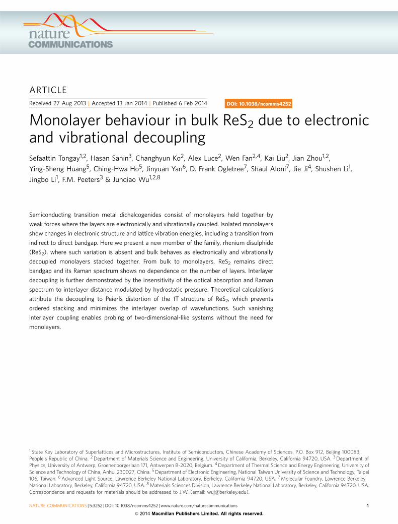
ResultsDFT calculations and calculated crystal structure. Figure 1ashows a comparison of the structure of a single layer of ReS2 withthe conventional 1H structure of sTMDs such as MoS2. For ReS2,
DFT calculations show that the hexagonal (H) phase is unstable,whereas the octahedral (T) phase goes through the Peierlsdistortion, resulting in buckled S layers and zigzag Re chains alongone of the lattice vectors in the plane (Fig. 1a bottom,Supplementary Fig. 1). The resultant lattice in Fig. 1a can beregarded as a distorted 1T structure (Supplementary Notes 1 and 2).Owing to the reduced crystal symmetry, ReS2 displays a morecomplex Raman spectrum than conventional sTMDs, as will bediscussed later. DFT calculations reveal that bulk and monolayerReS2 have nearly identical band structures (Fig. 1b), both beingdirect-bandgap semiconductors with a predicted generalized gra-dient approximation (GGA) bandgap at Egap¼ 1.35 eV (bulk) and1.43 eV (monolayer), respectively (Supplementary Note 3). This isin stark contrast to conventional sTMDs, where the band structureis strongly dependent on the number of layers4,5. Our DFTcalculations (Fig. 1c) also show that adjacent layers in ReS2 areindeed only weakly coupled to each other, with a coupling energyofB18 meV per unit cell, o8% of that of MoS2 (460 meV for thecorresponding 2� 2 conventional cell).
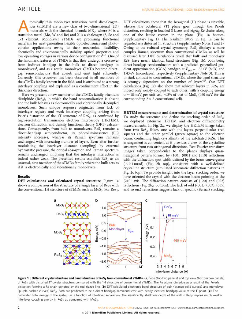
HRTEM measurements and determination of crystal structure.To study the structure and define the stacking order of ReS2,we deployed extensive HRTEM and electron diffractometrymeasurements. In Fig. 2a, we display the HRTEM image takenfrom two ReS2 flakes, one with the layers perpendicular (redsquare) and the other parallel (green square) to the electronbeam, confirming high crystallinity of the exfoliated ReS2. Thisarrangement is convenient as it provides a view of the crystallinestructure from two orthogonal directions. Fast Fourier transformimages taken perpendicular to the planes displays quasi-hexagonal pattern formed by (100), (001) and (110) reflectionswith the diffraction spot width defined by the beam convergence(B0.1 mrad) (Fig. 2b top), consistent with a well-definedcrystalline structure (simulated kinematic diffraction patterns inFig. 2c top). To provide insight into the layer stacking order, wehave oriented the crystal with the electron beam pointing at the[210] axis. The diffraction pattern consists of (1�20) and (002)reflections (Fig. 2b,c bottom). The lack of odd ((001), (003), (005)and so on.) reflections suggests lack of specific (Bernal) stacking,
MoS2 1.5
0
0.1
0.2
Ene
rgy
(eV
)
0.3
0.4
2 3 6 7 8 9
Inter-layer distance (Å)
4 5
1.0
0.5 BulkMonolayer
460 meV
ReS2
18 meV
MoS2
Egap0.0
– 0.5
Ene
rgy
(eV
)
–1.0
–1.5
–2.0
K′ M′L
MoS2
ReS2
ReS2
′
Figure 1 | Different crystal structure and band structure of ReS2 from conventional sTMDs. (a) Side (top two panels) and top view (bottom two panels)
of ReS2 with distorted 1T crystal structure compared with the 1H structure of conventional sTMDs. The Re atoms dimerize as a result of the Peierls
distortion forming a Re chain denoted by the red zigzag line. (b) DFT calculated electronic band structure of bulk (orange solid curves) and monolayer
(purple dashed curves) ReS2. Both are predicted to be a direct bandgap semiconductor with nearly identical bandgap value at the G point. (c) The
calculated total energy of the system as a function of interlayer separation. The significantly shallower depth of the well in ReS2 implies much weaker
interlayer coupling energy in ReS2 as compared with MoS2.
ARTICLE NATURE COMMUNICATIONS | DOI: 10.1038/ncomms4252
2 NATURE COMMUNICATIONS | 5:3252 | DOI: 10.1038/ncomms4252 | www.nature.com/naturecommunications
& 2014 Macmillan Publishers Limited. All rights reserved.
unlike in 2H-MoS2 that possesses Bernal stacking between thelayers. The (0,0,2l) reflections are inhomogeneously broadenedboth in the 001 and (1�20) directions. Nano-beam electron dif-fraction pattern in Fig. 2d and inset allow direct comparison ofthe broadening because of the particular sample geometry. Forsimplicity, we attribute all the inhomogeneous broadening of the0,0,2l reflections to fluctuation in interlayer distance. From thisanalysis, the interlayer spacing is determined to vary between 6.0and 6.9 Å. This reduced degree of crystallinity is not turbostraticin nature; rather, it is a consequence of weak interlayer bondingwith small in-plane displacements from equilibrium position(Supplementary Notes 1,2 and 7).
Comparison between PL behaviour of ReS2 versus othersTMDs. Considering such contrast in the crystal structure, wenext focus experimentally on the physical properties of ReS2
flakes. Mono- and multilayer ReS2 were mechanically exfoliatedfrom synthetic bulk crystals (see Methods section for crystalgrowth) onto Si substrates with 90 nm thermal oxide6. TheseReS2 flakes were characterized using atomic force microscopy(AFM), Raman spectroscopy, micro-PL (mPL), and nano-Augerelectron spectroscopy (AES). Nano-AES elemental compositionanalysis revealed an S/Re ratio of 1.98±0.10 (SupplementaryFig. 8, Supplementary Note 6). Tapping-mode AFM scan typicallyyielded 0.7 nm thickness for the monolayers. For comparison,monolayers and multilayers of conventional sTMDs (MoS2,
MoSe2, WSe2 and WS2) were also prepared by mechanicalexfoliation from bulk crystals.
All ReS2 flakes exhibit mPL at room temperature with a peak inthe range of 1.5–1.6 eV. The peak energy increases slightly (byo10%) for an isolated monolayer (Fig. 3a). The integrated PLintensity increases with the number of layers, and starts tosaturate for flakes thicker than six layers, as shown in Fig. 3b. Thisis in stark contrast to the behaviour observed in conventionalsTMDs such as MoS2 (ref. 4), MoSe2 (ref. 7), WS2 and WSe2
(ref. 8), where the monolayer PL intensity is enhanced by ordersof magnitude as a result of the crossover from an indirectbandgap in the bulk to a direct bandgap in monolayers. In thoseMo and W systems, the PL in the indirect-bandgap multilayersarises from hot luminescence4 across the wider direct bandgap,and is exponentially weaker in thicker layers. In addition, the PLpeak position of these conventional sTMDs increases drasticallyby 30–60% for thinner layers (Fig. 3c), which can be explained bystronger out-of-plane quantum confinement with decreasingthickness4. In contrast, the PL peak of ReS2 is nearly independentof the number of layers, indicating that thinning down the flakedoes not enhance the quantum confinement of electrons in thesystem, and that neighbouring monolayers in the flake are alreadylargely electronically decoupled.
Electronic decoupling in ReS2. To further test the interlayerdecoupling in ReS2, we modulate its interlayer distance by
ZA [001]
ZA [210]
(110)
(010)
(100)
(120) (122)
(004)(220)
21nm(002)
Figure 2 | Structural characterization of ReS2. (a) HRTEM images taken from ReS2 along in- and out-of-plane directions. There are two flakes: one
flake’s basal plane is perpendicular to the electron beam (red square box) and the other flake’s basal plane is oriented parallel to the beam (green square
box). Scale bar, 20 nm. (b) Fast Fourier transform images from the denoted red/green windows. (c) Simulated kinematic diffraction patterns, and
(d) nano-beam electron diffraction pattern. Inset: Zoom-in image to the nano-beam electron diffraction pattern.
NATURE COMMUNICATIONS | DOI: 10.1038/ncomms4252 ARTICLE
NATURE COMMUNICATIONS | 5:3252 | DOI: 10.1038/ncomms4252 | www.nature.com/naturecommunications 3
& 2014 Macmillan Publishers Limited. All rights reserved.
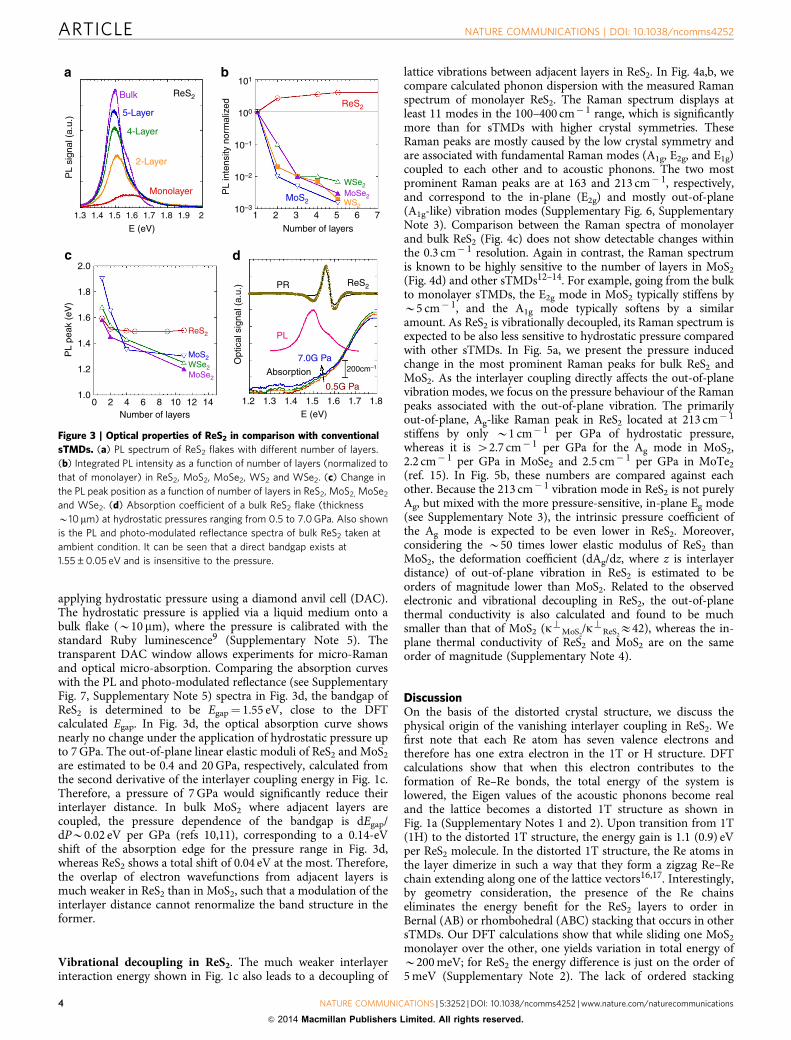
applying hydrostatic pressure using a diamond anvil cell (DAC).The hydrostatic pressure is applied via a liquid medium onto abulk flake (B10 mm), where the pressure is calibrated with thestandard Ruby luminescence9 (Supplementary Note 5). Thetransparent DAC window allows experiments for micro-Ramanand optical micro-absorption. Comparing the absorption curveswith the PL and photo-modulated reflectance (see SupplementaryFig. 7, Supplementary Note 5) spectra in Fig. 3d, the bandgap ofReS2 is determined to be Egap¼ 1.55 eV, close to the DFTcalculated Egap. In Fig. 3d, the optical absorption curve showsnearly no change under the application of hydrostatic pressure upto 7 GPa. The out-of-plane linear elastic moduli of ReS2 and MoS2
are estimated to be 0.4 and 20 GPa, respectively, calculated fromthe second derivative of the interlayer coupling energy in Fig. 1c.Therefore, a pressure of 7 GPa would significantly reduce theirinterlayer distance. In bulk MoS2 where adjacent layers arecoupled, the pressure dependence of the bandgap is dEgap/dPB0.02 eV per GPa (refs 10,11), corresponding to a 0.14-eVshift of the absorption edge for the pressure range in Fig. 3d,whereas ReS2 shows a total shift of 0.04 eV at the most. Therefore,the overlap of electron wavefunctions from adjacent layers ismuch weaker in ReS2 than in MoS2, such that a modulation of theinterlayer distance cannot renormalize the band structure in theformer.
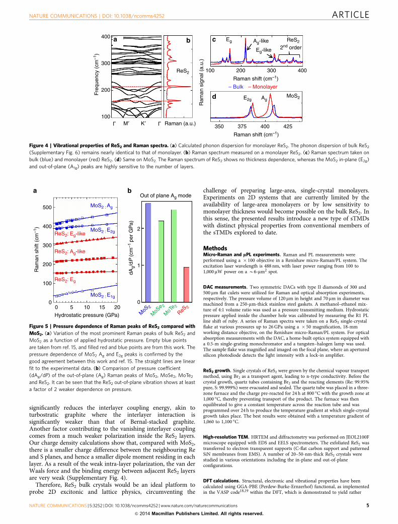
Vibrational decoupling in ReS2. The much weaker interlayerinteraction energy shown in Fig. 1c also leads to a decoupling of
lattice vibrations between adjacent layers in ReS2. In Fig. 4a,b, wecompare calculated phonon dispersion with the measured Ramanspectrum of monolayer ReS2. The Raman spectrum displays atleast 11 modes in the 100–400 cm� 1 range, which is significantlymore than for sTMDs with higher crystal symmetries. TheseRaman peaks are mostly caused by the low crystal symmetry andare associated with fundamental Raman modes (A1g, E2g, and E1g)coupled to each other and to acoustic phonons. The two mostprominent Raman peaks are at 163 and 213 cm� 1, respectively,and correspond to the in-plane (E2g) and mostly out-of-plane(A1g-like) vibration modes (Supplementary Fig. 6, SupplementaryNote 3). Comparison between the Raman spectra of monolayerand bulk ReS2 (Fig. 4c) does not show detectable changes withinthe 0.3 cm� 1 resolution. Again in contrast, the Raman spectrumis known to be highly sensitive to the number of layers in MoS2
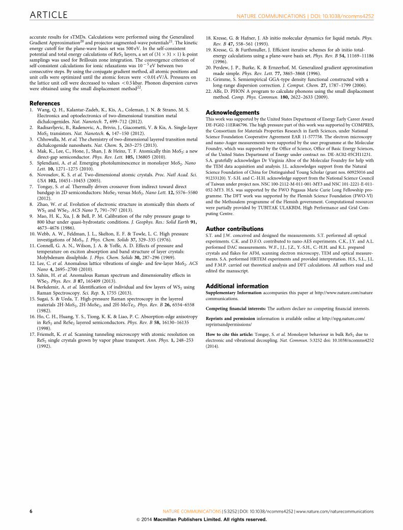
(Fig. 4d) and other sTMDs12–14. For example, going from the bulkto monolayer sTMDs, the E2g mode in MoS2 typically stiffens byB5 cm� 1, and the A1g mode typically softens by a similaramount. As ReS2 is vibrationally decoupled, its Raman spectrum isexpected to be also less sensitive to hydrostatic pressure comparedwith other sTMDs. In Fig. 5a, we present the pressure inducedchange in the most prominent Raman peaks for bulk ReS2 andMoS2. As the interlayer coupling directly affects the out-of-planevibration modes, we focus on the pressure behaviour of the Ramanpeaks associated with the out-of-plane vibration. The primarilyout-of-plane, Ag-like Raman peak in ReS2 located at 213 cm� 1
stiffens by only B1 cm� 1 per GPa of hydrostatic pressure,whereas it is 42.7 cm� 1 per GPa for the Ag mode in MoS2,2.2 cm� 1 per GPa in MoSe2 and 2.5 cm� 1 per GPa in MoTe2
(ref. 15). In Fig. 5b, these numbers are compared against eachother. Because the 213 cm� 1 vibration mode in ReS2 is not purelyAg, but mixed with the more pressure-sensitive, in-plane Eg mode(see Supplementary Note 3), the intrinsic pressure coefficient ofthe Ag mode is expected to be even lower in ReS2. Moreover,considering the B50 times lower elastic modulus of ReS2 thanMoS2, the deformation coefficient (dAg/dz, where z is interlayerdistance) of out-of-plane vibration in ReS2 is estimated to beorders of magnitude lower than MoS2. Related to the observedelectronic and vibrational decoupling in ReS2, the out-of-planethermal conductivity is also calculated and found to be muchsmaller than that of MoS2 (k>MoS2
/k>ReS2E42), whereas the in-
plane thermal conductivity of ReS2 and MoS2 are on the sameorder of magnitude (Supplementary Note 4).
DiscussionOn the basis of the distorted crystal structure, we discuss thephysical origin of the vanishing interlayer coupling in ReS2. Wefirst note that each Re atom has seven valence electrons andtherefore has one extra electron in the 1T or H structure. DFTcalculations show that when this electron contributes to theformation of Re–Re bonds, the total energy of the system islowered, the Eigen values of the acoustic phonons become realand the lattice becomes a distorted 1T structure as shown inFig. 1a (Supplementary Notes 1 and 2). Upon transition from 1T(1H) to the distorted 1T structure, the energy gain is 1.1 (0.9) eVper ReS2 molecule. In the distorted 1T structure, the Re atoms inthe layer dimerize in such a way that they form a zigzag Re–Rechain extending along one of the lattice vectors16,17. Interestingly,by geometry consideration, the presence of the Re chainseliminates the energy benefit for the ReS2 layers to order inBernal (AB) or rhombohedral (ABC) stacking that occurs in othersTMDs. Our DFT calculations show that while sliding one MoS2
monolayer over the other, one yields variation in total energy ofB200 meV; for ReS2 the energy difference is just on the order of5 meV (Supplementary Note 2). The lack of ordered stacking
PL
sign
al (
a.u.
)
ReS2Bulk
MoSe2
MoSe2
5-Layer
MoS2
4-Layer
WSe2
WSe2
MoS2
7.0G Pa
0.5G Pa
2-Layer
WS2
Monolayer
ReS2 PL
ReS2
1.3
2.0
1.8
1.6
1.4
PL
peak
(eV
)
1.2
1.00 2 4 6 8 10 12 14
Number of layers
1.4 1.5 1.6 1.7
E (eV)
10–3
Opt
ical
sig
nal (
a.u.
)
1 2 3 5 6 74
1.2 1.3 1.4 1.5 1.6 1.7 1.8E (eV)
200cm–1Absorption
PR ReS2
Number of layers
10–2
10–1
100
101
PL
inte
nsity
nor
mal
ized
1.8 1.9 2
Figure 3 | Optical properties of ReS2 in comparison with conventional
sTMDs. (a) PL spectrum of ReS2 flakes with different number of layers.
(b) Integrated PL intensity as a function of number of layers (normalized to
that of monolayer) in ReS2, MoS2, MoSe2, WS2 and WSe2. (c) Change in
the PL peak position as a function of number of layers in ReS2, MoS2, MoSe2
and WSe2. (d) Absorption coefficient of a bulk ReS2 flake (thickness
B10mm) at hydrostatic pressures ranging from 0.5 to 7.0 GPa. Also shown
is the PL and photo-modulated reflectance spectra of bulk ReS2 taken at
ambient condition. It can be seen that a direct bandgap exists at
1.55±0.05 eV and is insensitive to the pressure.
ARTICLE NATURE COMMUNICATIONS | DOI: 10.1038/ncomms4252
4 NATURE COMMUNICATIONS | 5:3252 | DOI: 10.1038/ncomms4252 | www.nature.com/naturecommunications
& 2014 Macmillan Publishers Limited. All rights reserved.
significantly reduces the interlayer coupling energy, akin toturbostratic graphite where the interlayer interaction issignificantly weaker than that of Bernal-stacked graphite.Another factor contributing to the vanishing interlayer couplingcomes from a much weaker polarization inside the ReS2 layers.Our charge density calculations show that, compared with MoS2,there is a smaller charge difference between the neighbouring Reand S planes, and hence a smaller dipole moment residing in eachlayer. As a result of the weak intra-layer polarization, the van derWaals force and the binding energy between adjacent ReS2 layersare very weak (Supplementary Fig. 4).
Therefore, ReS2 bulk crystals would be an ideal platform toprobe 2D excitonic and lattice physics, circumventing the
challenge of preparing large-area, single-crystal monolayers.Experiments on 2D systems that are currently limited by theavailability of large-area monolayers or by low sensitivity tomonolayer thickness would become possible on the bulk ReS2. Inthis sense, the presented results introduce a new type of sTMDswith distinct physical properties from conventional members ofthe sTMDs explored to date.
MethodsMicro-Raman and lPL experiments. Raman and PL measurements wereperformed using a � 100 objective in a Renishaw micro-Raman/PL system. Theexcitation laser wavelength is 488 nm, with laser power ranging from 100 to1,000 mW power on a B6-mm2 spot.
DAC measurements. Two symmetric DACs with type II diamonds of 300 and500 mm flat culets were utilized for Raman and optical absorption experiments,respectively. The pressure volume of 120mm in height and 70mm in diameter wasmachined from a 250-mm-thick stainless steel gaskets. A methanol–ethanol mix-ture of 4:1 volume ratio was used as a pressure transmitting medium. Hydrostaticpressure applied inside the chamber hole was calibrated by measuring the R1 PLline shift of ruby. A series of Raman spectra were taken on a ReS2 single-crystalflake at various pressures up to 26 GPa using a � 50 magnification, 18-mmworking distance objective, on the Renishaw micro-Raman/PL system. For opticalabsorption measurements with the DAC, a home-built optics system equipped witha 0.5-m single-grating monochromator and a tungsten–halogen lamp was used.The sample flake was magnified and imaged on the focal plane, where an aperturedsilicon photodiode detects the light intensity with a lock-in amplifier.
ReS2 growth. Single crystals of ReS2 were grown by the chemical vapour transportmethod, using Br2 as a transport agent, leading to n-type conductivity. Before thecrystal growth, quartz tubes containing Br2 and the reacting elements (Re: 99.95%pure, S: 99.999%) were evacuated and sealed. The quartz tube was placed in a three-zone furnace and the charge pre-reacted for 24 h at 800 �C with the growth zone at1,000 �C, thereby preventing transport of the product. The furnace was thenequilibrated to give a constant temperature across the reaction tube and wasprogrammed over 24 h to produce the temperature gradient at which single-crystalgrowth takes place. The best results were obtained with a temperature gradient of1,060 to 1,100 �C.
High-resolution TEM. HRTEM and diffractometry was performed on JEOL2100Fmicroscope equipped with EDS and EELS spectrometers. The exfoliated ReS2 wastransferred to electron transparent supports (C-flat carbon support and patternedSiN membranes from EMS). A number of 20–50-nm-thick ReS2 crystals werestudied in various orientations including the in-plane and out-of-planeconfigurations.
DFT calculations. Structural, electronic and vibrational properties have beencalculated using GGA-PBE (Perdew-Burke-Ernzerhof) functional, as implementedin the VASP code18,19 within the DFT, which is demonstrated to yield rather
400 Eg
E2g
– Bulk – Monolayer
100
400 425
Raman shift (cm–1)
350 375
200
Raman shift (cm–1)
300 400
Ag-like
Ag
Eg-like 2nd orderReS2
MoS2
300
Ram
an s
igna
l (a.
u.)
200Fr
eque
ncy
(cm
–1)
100M′ K′
ReS2
Raman (a.u.)L L
Figure 4 | Vibrational properties of ReS2 and Raman spectra. (a) Calculated phonon dispersion for monolayer ReS2. The phonon dispersion of bulk ReS2
(Supplementary Fig. 6) remains nearly identical to that of monolayer. (b) Raman spectrum measured on a monolayer ReS2. (c) Raman spectrum taken on
bulk (blue) and monolayer (red) ReS2. (d) Same on MoS2. The Raman spectrum of ReS2 shows no thickness dependence, whereas the MoS2 in-plane (E2g)
and out-of-plane (A1g) peaks are highly sensitive to the number of layers.
500
Out of plane Ag mode
2
dAg/
dP (
cm–1
per
GP
a)
1
0
MoS
2
MoS2 : E1g
MoS2 : E2g
MoS2 : Ag
MoS
e 2
MoT
e 2
ReS2
400
300
200
100
Ram
an s
hift
(cm
–1)
00 5
ReS2: Eg
ReS2: Ag-like
ReS2: Eg-like
10 15 20
Hydrostatic pressure (GPa)
Figure 5 | Pressure dependence of Raman peaks of ReS2 compared with
MoS2. (a) Variation of the most prominent Raman peaks of bulk ReS2 and
MoS2 as a function of applied hydrostatic pressure. Empty blue points
are taken from ref. 15, and filled red and blue points are from this work. The
pressure dependence of MoS2 Ag and E2g peaks is confirmed by the
good agreement between this work and ref. 15. The straight lines are linear
fit to the experimental data. (b) Comparison of pressure coefficient
(dAg/dP) of the out-of-plane (Ag) Raman peaks of MoS2, MoSe2, MoTe2
and ReS2. It can be seen that the ReS2 out-of-plane vibration shows at least
a factor of 2 weaker dependence on pressure.
NATURE COMMUNICATIONS | DOI: 10.1038/ncomms4252 ARTICLE
NATURE COMMUNICATIONS | 5:3252 | DOI: 10.1038/ncomms4252 | www.nature.com/naturecommunications 5
& 2014 Macmillan Publishers Limited. All rights reserved.
accurate results for sTMDs. Calculations were performed using the GeneralizedGradient Approximation20 and projector augmented-wave potentials21. The kineticenergy cutoff for the plane-wave basis set was 500 eV. In the self-consistentpotential and total energy calculations of ReS2 layers, a set of (31� 31� 1) k-pointsamplings was used for Brillouin zone integration. The convergence criterion ofself-consistent calculations for ionic relaxations was 10� 5 eV between twoconsecutive steps. By using the conjugate gradient method, all atomic positions andunit cells were optimized until the atomic forces were o0.01 eV/Å. Pressures onthe lattice unit cell were decreased to values o0.5 kbar. Phonon dispersion curveswere obtained using the small displacement method22.
References1. Wang, Q. H., Kalantar-Zadeh, K., Kis, A., Coleman, J. N. & Strano, M. S.
Electronics and optoelectronics of two-dimensional transition metaldichalcogenides. Nat. Nanotech. 7, 699–712 (2012).
2. Radisavljevic, B., Radenovic, A., Brivio, J., Giacometti, V. & Kis, A. Single-layerMoS2 transistors. Nat. Nanotech. 6, 147–150 (2012).
3. Chhowalla, M. et al. The chemistry of two-dimensional layered transition metaldichalcogenide nanosheets. Nat. Chem. 5, 263–275 (2013).
4. Mak, K., Lee, C., Hone, J., Shan, J. & Heinz, T. F. Atomically thin MoS2: a newdirect-gap semiconductor. Phys. Rev. Lett. 105, 136805 (2010).
5. Splendiani, A. et al. Emerging photoluminescence in monolayer MoS2. NanoLett. 10, 1271–1275 (2010).
6. Novoselov, K. S. et al. Two-dimensional atomic crystals. Proc. Natl Acad. Sci.USA 102, 10451–10453 (2005).
7. Tongay, S. et al. Thermally driven crossover from indirect toward directbandgap in 2D semiconductors: MoSe2 versus MoS2. Nano Lett. 12, 5576–5580(2012).
8. Zhao, W. et al. Evolution of electronic structure in atomically thin sheets ofWS2 and WSe2. ACS Nano 7, 791–797 (2013).
9. Mao, H. K., Xu, J. & Bell, P. M. Calibration of the ruby pressure gauge to800 kbar under quasi-hydrostatic conditions. J. Geophys. Res.: Solid Earth 91,4673–4676 (1986).
10. Webb, A. W., Feldman, J. L., Skelton, E. F. & Towle, L. C. High pressureinvestigations of MoS2. J. Phys. Chem. Solids 37, 329–335 (1976).
11. Connell, G. A. N., Wilson, J. A. & Yoffe, A. D. Effects of pressure andtemperature on exciton absorption and band structure of layer crystals:Molybdenum disulphide. J. Phys. Chem. Solids 30, 287–296 (1969).
12. Lee, C. et al. Anomalous lattice vibrations of single- and few-layer MoS2. ACSNano 4, 2695–2700 (2010).
13. Sahin, H. et al. Anomalous Raman spectrum and dimensionality effects inWSe2. Phys. Rev. B 87, 165409 (2013).
14. Berkdemir, A. et al. Identification of individual and few layers of WS2 usingRaman Spectroscopy. Sci. Rep. 3, 1755 (2013).
15. Sugai, S. & Ueda, T. High-pressure Raman spectroscopy in the layeredmaterials 2H-MoS2, 2H-MoSe2, and 2H-MoTe2. Phys. Rev. B 26, 6554–6558(1982).
16. Ho, C. H., Huang, Y. S., Tiong, K. K. & Liao, P. C. Absorption-edge anisotropyin ReS2 and ReSe2 layered semiconductors. Phys. Rev. B 58, 16130–16135(1998).
17. Friemelt, K. et al. Scanning tunneling microscopy with atomic resolution onReS2 single crystals grown by vapor phase transport. Ann. Phys. 1, 248–253(1992).
18. Kresse, G. & Hafner, J. Ab initio molecular dynamics for liquid metals. Phys.Rev. B 47, 558–561 (1993).
19. Kresse, G. & Furthmuller, J. Efficient iterative schemes for ab initio total-energy calculations using a plane-wave basis set. Phys. Rev. B 54, 11169–11186(1996).
20. Perdew, J. P., Burke, K. & Ernzerhof, M. Generalized gradient approximationmade simple. Phys. Rev. Lett. 77, 3865–3868 (1996).
21. Grimme, S. Semiempirical GGA-type density functional constructed with along-range dispersion correction. J. Comput. Chem. 27, 1787–1799 (2006).
22. Alfe, D. PHON A program to calculate phonons using the small displacementmethod. Comp. Phys. Commun. 180, 2622–2633 (2009).
AcknowledgementsThis work was supported by the United States Department of Energy Early Career AwardDE-FG02-11ER46796. The high pressure part of this work was supported by COMPRES,the Consortium for Materials Properties Research in Earth Sciences, under NationalScience Foundation Cooperative Agreement EAR 11-577758. The electron microscopyand nano-Auger measurements were supported by the user programme at the MolecularFoundry, which was supported by the Office of Science, Office of Basic Energy Sciences,of the United States Department of Energy under contract no. DE-AC02-05CH11231.S.A. gratefully acknowledges Dr Virginia Altoe of the Molecular Foundry for help withthe TEM data acquisition and analysis. J.L. acknowledges support from the NaturalScience Foundation of China for Distinguished Young Scholar (grant nos. 60925016 and91233120). Y.-S.H. and C.-H.H. acknowledge support from the National Science Councilof Taiwan under project nos. NSC 100-2112-M-011-001-MY3 and NSC 101-2221-E-011-052-MY3. H.S. was supported by the FWO Pegasus Marie Curie Long Fellowship pro-gramme. The DFT work was supported by the Flemish Science Foundation (FWO-Vl)and the Methusalem programme of the Flemish government. Computational resourceswere partially provided by TUBITAK ULAKBIM, High Performance and Grid Com-puting Centre.
Author contributionsS.T. and J.W. conceived and designed the measurements. S.T. performed all opticalexperiments. C.K. and D.F.O. contributed to nano-AES experiments. C.K., J.Y. and A.L.performed DAC measurements. W.F., J.J., J.Z., Y.-S.H., C.-H.H. and K.L. preparedcrystals and flakes for AFM, scanning electron microscopy, TEM and optical measure-ments. S.A. performed HRTEM experiments and provided interpretation. H.S., S.L., J.L.and F.M.P. carried out theoretical analysis and DFT calculations. All authors read andedited the manuscript.
Additional informationSupplementary Information accompanies this paper at http://www.nature.com/naturecommunications.
Competing financial interests: The authors declare no competing financial interests.
Reprints and permission information is available online at http://npg.nature.com/reprintsandpermissions/
How to cite this article: Tongay, S. et al. Monolayer behaviour in bulk ReS2 due toelectronic and vibrational decoupling. Nat. Commun. 5:3252 doi: 10.1038/ncomms4252(2014).
ARTICLE NATURE COMMUNICATIONS | DOI: 10.1038/ncomms4252
6 NATURE COMMUNICATIONS | 5:3252 | DOI: 10.1038/ncomms4252 | www.nature.com/naturecommunications
& 2014 Macmillan Publishers Limited. All rights reserved.
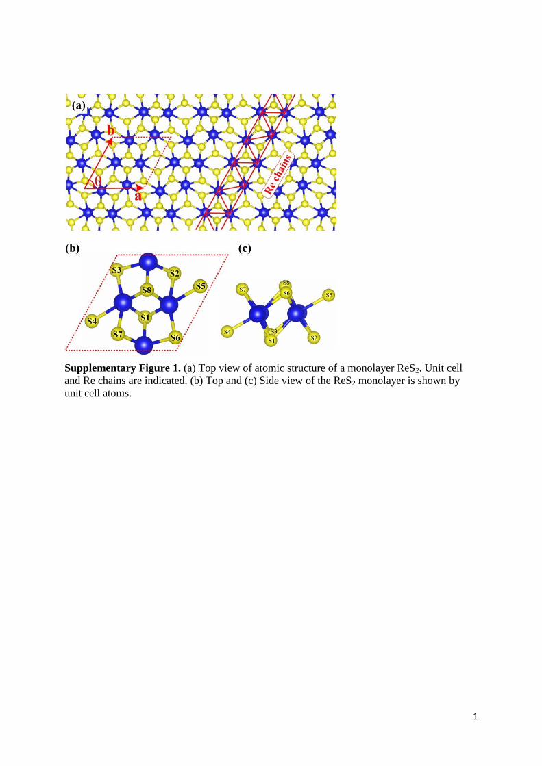
1
Supplementary Figure 1. (a) Top view of atomic structure of a monolayer ReS2. Unit cell
and Re chains are indicated. (b) Top and (c) Side view of the ReS2 monolayer is shown by
unit cell atoms.
2
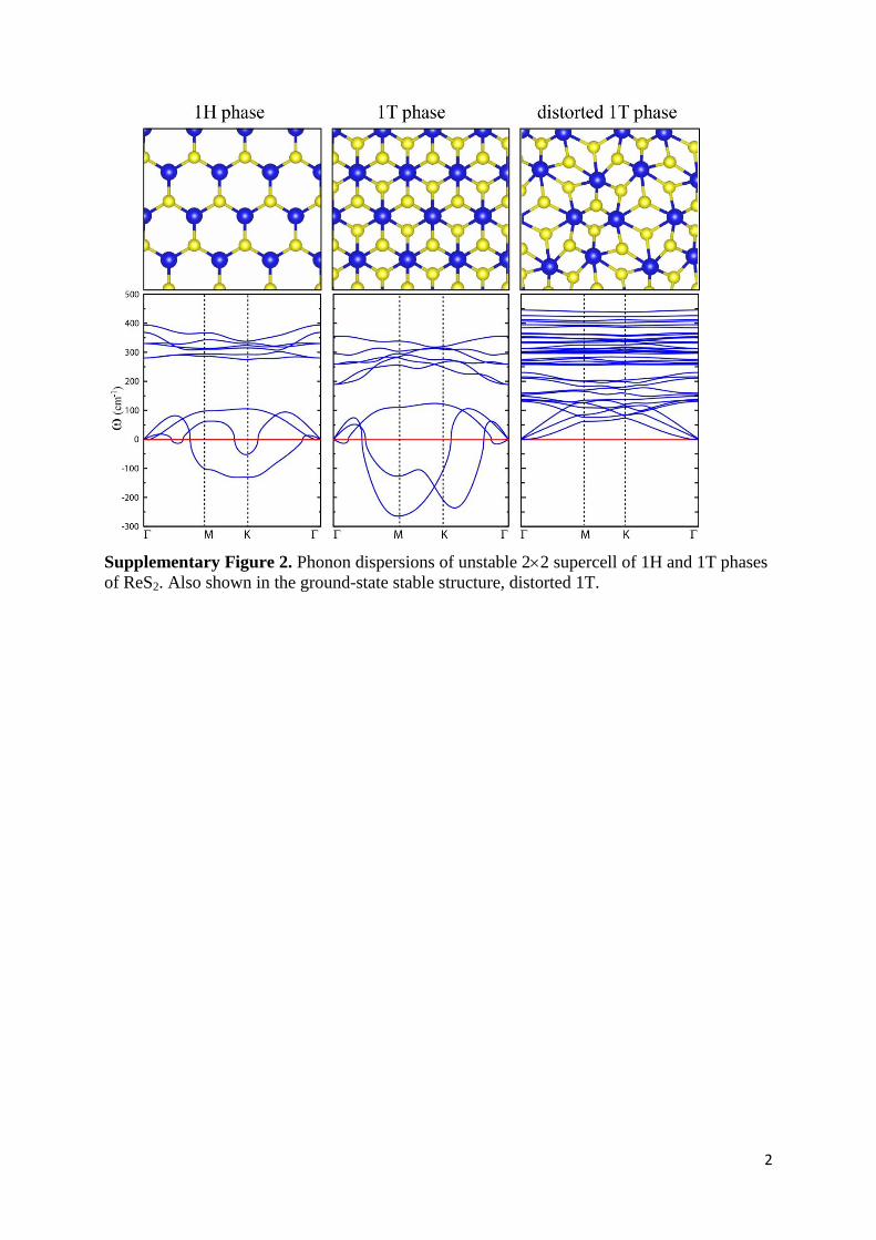
Supplementary Figure 2. Phonon dispersions of unstable 22 supercell of 1H and 1T phases
of ReS2. Also shown in the ground-state stable structure, distorted 1T.
3
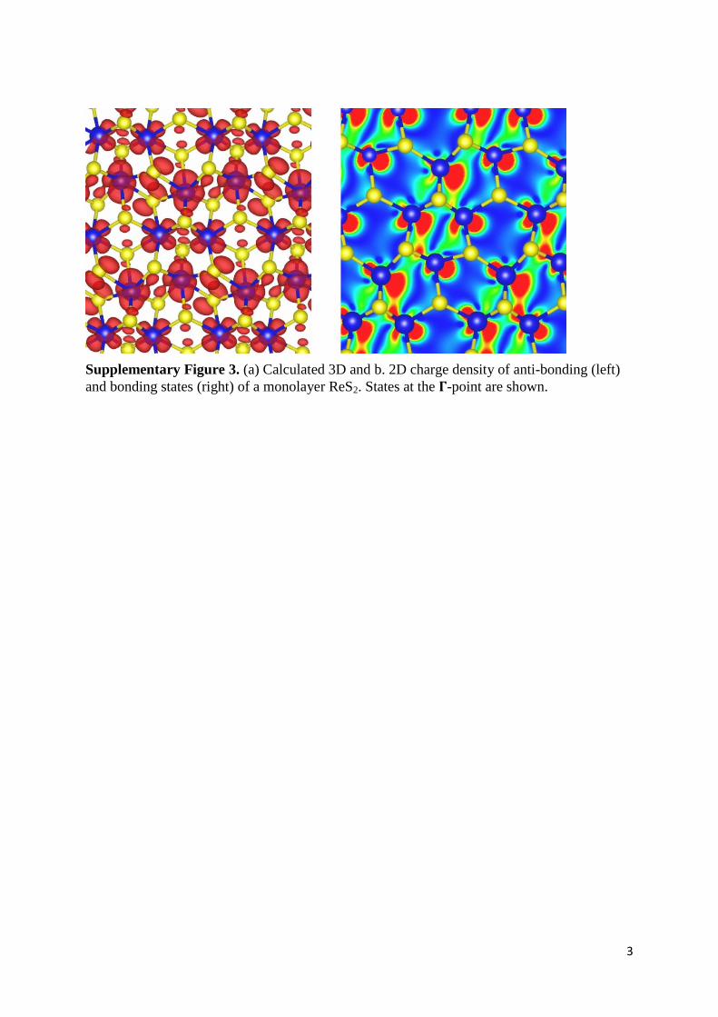
Supplementary Figure 3. (a) Calculated 3D and b. 2D charge density of anti-bonding (left)
and bonding states (right) of a monolayer ReS2. States at the 𝚪-point are shown.
4
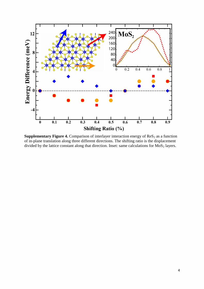
Supplementary Figure 4. Comparison of interlayer interaction energy of ReS2 as a function
of in-plane translation along three different directions. The shifting ratio is the displacement
divided by the lattice constant along that direction. Inset: same calculations for MoS2 layers.
5
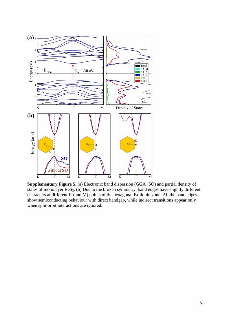
Supplementary Figure 5. (a) Electronic band dispersion (GGA+SO) and partial density of
states of monolayer ReS2. (b) Due to the broken symmetry, band edges have slightly different
characters at different K (and M) points of the hexagonal Brillouin zone. All the band edges
show semiconducting behaviour with direct bandgap, while indirect transitions appear only
when spin-orbit interactions are ignored.
6
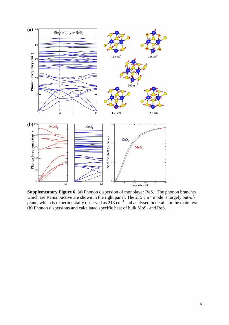
Supplementary Figure 6. (a) Phonon dispersion of monolayer ReS2. The phonon branches
which are Raman-active are shown in the right panel. The 215 cm-1
mode is largely out-of-
plane, which is experimentally observed as 213 cm-1
and analysed in details in the main text.
(b) Phonon dispersions and calculated specific heat of bulk MoS2 and ReS2.
7
167
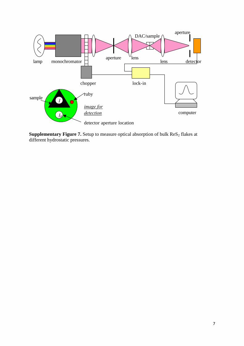
The experimental setup of optical absorption with the DAC is shown
schematically in Fig. A6. The sample in the tiny pressurized volume is magnified (́ ~
50) through a short- focus lens. Near the focal plane, an enlarged image of the sample and
surrounding empty area in the pressurized volume is obtained. A small aperture is
inserted into the image plane, through which the light intensity can be selectively
detected. As shown in Fig. A6, when the aperture is placed in the shadow of the sample,
the photon flux intensity is scanned and recorded as I; when the aperture is located in the
empty area, I0 is recorded. The absorption coefficient a is then calculated as
( )( )( )w
wwa
I
I
d
0ln1
=h ,
with d the sample thickness.
Fig. A6. Optics for absorption experiment with a DAC. The left lower part
shows the schematic image of the sample area in the detector aperture
plane.
lamp
aperture
computer
chopper
lens lens monochromator
lock-in
aperture
DAC/sample
I0
I
image for
detection
sample ruby
detector aperture location
detector
Supplementary Figure 7. Setup to measure optical absorption of bulk ReS2 flakes at
different hydrostatic pressures.
8
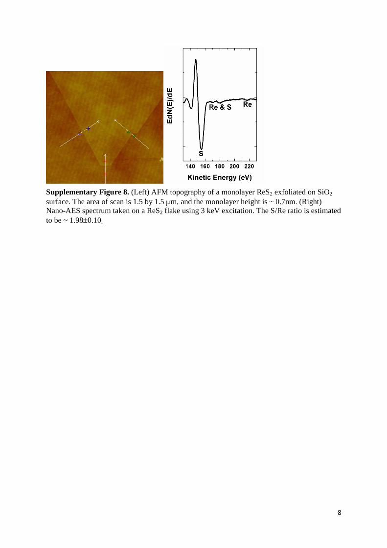
Supplementary Figure 8. (Left) AFM topography of a monolayer ReS2 exfoliated on SiO2
surface. The area of scan is 1.5 by 1.5 m, and the monolayer height is ~ 0.7nm. (Right)
Nano-AES spectrum taken on a ReS2 flake using 3 keV excitation. The S/Re ratio is estimated
to be ~ 1.980.10.
9
Supplementary Note 1. Lattice Structure of ReS2. Each ReS2 layer resembles the 1T crystal
structure, which is also the ground state of some other transition metal dichalcogenides
(TMDs), such as TaS2, TaSe2, TiS2, VSe2 and MnTe2. However, differing from these and
other sTMDs such as MoS2, MoSe2 and WSe2, ReS2 crystallizes in a distorted T structure
with clustering of Re4 units forming a one-dimensional chain inside each monolayer. The
formation of parallel chains of Re4 clusters in ReS2 causes a lattice distortion from the ideal
octahedral layered structure. In Fig. S1, we present the optimized atomic structure of ReS2.
The monolayer ReS2 can be thought as a distorted 1T structure. Due to metal-metal bonding,
the unit cell of ReS2 is doubled and therefore its primitive cell is composed of four Re and
eight S atoms. As shown in Fig. S1b, closer view of its atomic structure reveals that the S
atoms locate at four different distances from the Re layer. The formation of local Re chains
along the b lattice vector breaks the hexagonal lattice symmetry and makes this structure
special. In addition to the anisotropy between out-of-plane and in-plane crystal directions,
basal plane anisotropy along a and b lattice vectors can be observed.
Our vibrational analysis shown in Fig. S2, reveals that the periodic 1H and 1T structures of
ReS2 can be obtained by total energy optimization calculations. The calculated lattice
constants in H and T structures are 6.62 and 6.19 Å, respectively (22 super-cells of these
correspond to a unit cell of ReS2). The lattice parameters of ReS2 in distorted 1T phase are a =
6.51 and b = 6.41 Å. However, further examination of the stability of these structures shows
that the H and T structures of ReS2 are unstable, as their LA and ZA phonon modes have
imaginary eigen-frequencies. It is calculated that ReS2 single layer lowers its energy, 1.1 eV
(0.9) per ReS2 molecule, for a transition from 1T (1H) to distorted 1T phase. Clearly, both
energy optimization and phonon calculations reveal that ReS2 layers have distorted 1T phase
in their ground state.
The formation of Re chains can be understood via analysis of the bonding nature of ReS2.
As shown in Fig. S3, band decomposed charge density analysis shows that there is significant
amount of bond charges between the Re-Re dimers. It appears that each Re atom with seven
valence electrons would have one dangling electron in its 1T (and H) structure. Therefore,
obviously Re atoms lower the total energy of the system by making covalent bonds with each
other. As seen from Fig. S3, the reason for the formation of Re chains are the extra electrons
that result in strong covalent bonding between the Re atoms. However, the 5d-3p hybridized
bonding states provide interaction between adjacent Re chains. Therefore these Re chains are
further bonded to each other via S atoms.
Supplementary Note 2. Inter-layer Stacking of ReS2. We showed that differing from MoS2
bilayers that have 460 meV interlayer binding, ReS2 bilayers are weakly bonded to each other
with 18 meV. The interlayer binding of ReS2 layers is found to be small even by LDA
calculations that are known to give overestimate for these types of structures. For ReS2
(MoS2), calculated values of inter-layer binding energy per MX2 molecule by using GGA,
GGA+vdW and LDA exchange correlation functionals are 2 (58), 30 (76) and 38 (170) meV,
respectively. Our calculations also revealed that shifting one ReS2 monolayer over another
does not result in any significant change in total energy. With the translation along a, b lattice
vectors and along the diagonal direction of the unit cell, the energy difference between the
different stacking positions is negligibly small (at most 7 meV). These energies are shown in
Fig.S4.Therefore we can conclude that the interlayer interaction is extremely weak for
adjacent ReS2 layers and for the bulk (or multilayer) ReS2 structure; i.e., any kind of ordered
stacking is experimentally possible. Similar calculation of sliding MoS2 single-layer over the
other one (started from the ground state configuration) gives energy differences for different
positions in the order of 200 meV and rather large energy differences compared to ReS2.
10
The reason of the vanishing inter-layer coupling can be understood by analysis of charges
on each Re and S layer. Our results reveal that the Re layer becomes positively charged while
outermost S layers are negatively charged after the formation of the distorted 1T (1T*)
structure of ReS2. Here the situation is similar to 1H-MoS2. However, the charge difference
between Mo and S atoms is 1.8 electrons per unit cell, whereas in ReS2 this difference is just
0.4 electron/unit cell. Since the intra-layer polarization between Re and S layers is much
weaker than that between Mo and S layers, van der Waals (vdW) - like interaction is much
weaker in ReS2. Therefore, compared to Mo, the one dangling electron on the Re atom results
in less intra-layer polarization and weakens the vdW-like inter-layer interaction.
Supplementary Note 3. Electronic Structure and Lattice Dynamics. Bulk ReS2 is a
diamagnetic semiconductor crystallized in a distorted T structure of triclinic symmetry. Due
to its distorted layered lattice structure, anisotropic electrical and optical properties along a, b
and c lattice vectors can be expected. In Fig. S5 we present calculated electronic band
dispersion and partial density of states (DOS) for monolayer ReS2. It is seen that ReS2 has a
semiconducting band structure with a direct bandgap at the Γ point. From partial DOS
analysis we see that both the valence and conduction band edges are composed of Re-d and S-
p states. It is also worth to note that the majority of the states at these band edges originate
from Re-d states.
Differing from Figure.1b, in order to see how spin-orbit (SO) interaction influences the
band structure of ReS2, GGA+SO band dispersion is presented. It is seen that while the
dispersion of the bands do not change considerably, the bandgap of single layer ReS2
decreases from 1.43 to 1.30 eV. Since the perfect hexagonal unit cell of 1T structure is
disturbed after the formation of Re chains, corners of the Brillouin Zone of the distorted 1T
phase shifts negligibly. Moreover, zoomed-in plots for band edges in Fig. S5 reveal the
importance of inclusion of spin-orbit interactions in the distorted 1T phase. As long as SO
interactions are taken into account, band edges leads to a direct bandgap and therefore for a
correct description of band dispersion, inclusion of SO effects is essential.
For determination of the dispersion of phonon branches, we perform first-principles
calculations by using 48 and 96 atom unit cells for monolayer and bulk structures,
respectively. In Fig. S6 we take a closer look at the lattice dynamics of monolayer ReS2. As a
result of the lattice distortion, the lattice symmetry of ReS2 is broken and hence it has 36 non-
degenerate eigen-modes. In phonon dispersion of bulk ReS2 which is shown in Fig. S6b
number of modes is doubled. Although most of these are mixing of in-plane and out-of-plane
motion of Re and S atoms, certain modes have a more characteristic behaviour. The bond-
stretching nature of the modes at 152, 160 and 215 cm-1
implies the possibility for the
observation in Raman measurements. Our calculations displays twenty nine phonon branches
(fifty eight for bulk) in the 100 ~ 400 cm-1
range and we observe eleven of them as Raman-
active. It is also worth to note that because insufficient number of grid-points in the FFT-mesh
along the directions of c lattice-vector, lower-most acoustic mode has imaginary eigen-
frequency at the Γ point. This imaginary eigenvalue that has no physical meaning is just a
numerical artifact. Due to large computational cost of calculating phonons of such 48- and 96-
atomic systems with a very fine FFT-mesh, numerical error in lower-most modes was fixed
by quadratic fitting.
Supplementary Note 4. Thermal Conductivity of ReS2 and MoS2. In the main text, we
discuss that the weak interlayer coupling in ReS2 manifests itself as electronic and vibrational
decoupling; as a result, bulk ReS2 behaves as if monolayers. The discussed weak coupling
also suggests that out-of-plane thermal conductivity for ReS2 should be lower compared to
other sTMDs (such as MoS2) where the layers are coupled much stronger.
11
The thermal conductivity properties were calculated using Debye’s model. The lattice
thermal conductivity of a structure can be expressed by the κ = (1/3)Cvυ2τ where Cv, υ and τ
are specific heat, phonon velocity and phonon relaxation lifetime, respectively and the
effective phonon mean free path (MFP) is Λ= υτ. At high temperatures, almost all the phonon
modes become excited and Umklapp scattering becomes the dominant interaction process
between phonons. Around the Debye temperature, the most energetic phonon’s wavelength
approaches size of the unit cell size. In such case, Debye temperature (Θ) relates to the in-
plane lattice constant a and group velocity υ by the formal relation Θ=(2hυ)/(akB). Using the
experimentally available Debye temperature values (ΘMoS2=570 and ΘReS2=196 K)23-24
one
can extract the υ parameter.
In Fig.S6, we present volumetric specific heat Cv in units of kB per atom in the unit cell of
bulk ReS2 and MoS2 that are extracted from the calculated phonon dispersion relations. At the
same time, MFP ratio of ΛMoS2/ΛReS2 approaches the ratio of the average inter-atomic
distances aMoS2/aReS2 for relatively high temperatures. Using the CV, Λ, and υ ratios calculated
from experimentally available Debye temperature temperatures using the Θ=(2hυ)/(akB)
relation, the in-plane thermal conductivity of ReS2 and MoS2 (κMoS2/κReS2) has a ratio of 1.34.
It is generally known that the contribution of out-of-plane lattice vibrations to thermal
conductivity is rather small in layered materials such as graphene and sTMDs. The Slack’s
approach provides a successful model, and has been widely applied to various types of
semiconductors.25
Following Slack’s theory, out-of-plane κ can be given by κ =
(ℳBδΘD3)/(TγG
2N
2/3), where ℳ is the average atomic mass, B is a physical constant (3.1 ×
10−6
), δ3 is the average volume occupied by one atom of the crystal, ΘD is the Debye
temperature, γG is the Gruneisen parameter, and N is the number of atoms per unit cell. We
can calculate the Gruneisen parameter of each mode from the relative shift in the
corresponding branch γG,s = − (V/ωs)(∂ωs/∂V). Here ωs is the angular frequency of phonon of
the mode indexed by s, and V is the volume of the considered unit cell. Since the different
phonon branches show different dependence on the lattice expansion, one has to take the
averaged frequency shift over all the phonon modes that can contribute to cross-plane
conductivity. By doing so, the average value of the out-of-plane Gruneisen parameter is
calculated to be γ⊥MoS2= 0.5 for MoS2. Because of the broken symmetry and the larger unit
cell of the distorted-T structure of ReS2, we found ~50 phonon branches that all possibly
contribute to the out-of-plane heat conduction. For example, it is found that these modes
exhibit 0.9-4.2 cm−1
red shift under 0.002 lattice expansion. From these shifts, we calculated
γ⊥ReS2= 0.8. Combined with all other parameters, this yields κ⊥MoS2/κ⊥ReS2 42.
It is also worth noting that for layered materials, the presence of a ZO’ mode located just
above the acoustic modes is another indication of the strength of layer-layer coupling.26-27
For
instance, graphene’s ZO’ mode appears at 133 cm−1
, while for MoS2 it is at 50 cm−1
(See
Figure S6(b). However, because of the weak coupling between adjacent layers in ReS2, ZO’
mode is at 11 cm−1
, implying that the interlayer interaction is rather small compared to other
sTMDs (Figure S6(b)).
In conclusion, our results confirm that because of the weak interaction between the
adjacent ReS2 layers, out-of-plane thermal conductivity of ReS2 is more than an order
magnitude lower than MoS2. Such difference in the out-of-plane thermal conductivity is
mostly associated with differences in the Gruneisen parameter and Debye temperature.
Furthermore, the presence of corrugations and thermally excited distortions may lead to
symmetry breaking in lattice structures and therefore the symmetry selection rules, which
determine how phonons are scattered, may differ.
12
Supplementary Note 5. Micro-Absorption through the Diamond Anvil Cell (DAC) and
Photo-Modulated Reflectance. Optical absorption measurements were performed using a 0.5
m single-grating monochromator and a silicon photodiode detector. Figure S7 shows
experimental setup 28
. The sample in the tiny pressurized volume of the diamond anvil cell
(DAC) is magnified (by ~ 50) through a short-focus lens. Near the focal plane, a magnified
image of the sample and surrounding empty area in the pressurized volume is obtained. A
small aperture is inserted into the image plane, through which the light intensity can be
selectively detected. When the aperture is placed in the shadow of the sample, the light
intensity is scanned and recorded as I; when the aperture is located in the empty area, I0 is
recorded. The absorption coefficient α is then calculated as (h) =
ln[I0(h)]/ln[I(h)]/thickness. The reflection of the beam from the surface of the sample has
been assumed to vary slowly near the absorption edge and is neglected in the absorbance
calculation.
For high pressure experiments with the DACs, bulk flakes with a size of ~ 100100m and
thickness of ~ 10m were prepared, and mounted into gasketed DACs. The pressure medium
was a mixture of ethanol and methanol ~1:4. The applied pressure was calibrated by the
standard method of monitoring the red shift of the ruby R1 photoluminescence line.
Photo-modulated reflectance (PR) spectrum was taken at ambient conditions. The feature
shown corresponds to the critical point direct transition from the top of the valence bands to
the conduction band edge. The fundamental bandgap energy was determined from the PR
spectrum to be 1.57 eV, using the standard Aspenes fitting method 29
. This is in agreement
with the gap energy defined by the crossing point of the steeply rising portion and the baseline
of the micro-absorption curves, as well as the photoluminescence measurement. All optical
experiments were carried out at room temperature (295 K).
Supplementary Note 6. AFM and Nano-Auger Electron Spectroscopy (AES)
Measurements. The thicknesses of exfoliated layers were determined by AFM scanning
using a Digital-Instrument atomic force microscope. To estimate the chemical composition of
ReS2 single crystals, Auger spectroscopy was performed using a field emission electron
source and a multi-channel detector at ultra-high vacuum (low 10-10
mbar). A series of Auger
spectra were measured on several different regions with an electron beam energy of 3 keV
and a scan area of 50 μm × 50 μm. The S/Re stoichiometric ratio was estimated to be ~ 1.98
using the S 155 eV and Re 217 eV peaks and corresponding sensitivity factors, 4.7575 and
1.1260 30
.
Supplementary Note 7. High Resolution Transmission Electron Microscopy (HRTEM)
study. To study the structure and define the stacking order of ReS2, we deployed extensive
high-resolution transmission electron microscopy (HRTEM) and electron diffractometry. In
layered materials such as MoS2 and ReS2, the intensity of 00l electron diffraction spots carries
information about the stacking order. For example, 2H stacking in MoS2 will manifest itself
as a strong 6.05 Å (0 0 2l) reflections, representing the interlayer stacking distance, and
weaker (0 0 2l+1) reflections in between, resulting from the well-defined interlayer stacking.
For clarity and comparison, we chose to describe the ReS2 crystal by a 2T-ReS2 (ICSD
81814) unit cell, which is a triclinically distorted 2H-MoS2 structure consisting of two ReS2
layers per unit cell. The distortions with respect to the MoS2 cell are minor in the 001 and 100
directions, but are significant in the 010 axis, consistent with the Pearls distortion present in
the structure. The electron diffraction patterns in Fig.2 (main manuscript) reveal that the ReS2
crystal structure is similar to the structure files reported in the literature. Our TEM data show
that these ReS2 flakes are highly crystalline. Presence of high-intensity h0l and 0kl diffraction
peaks (from prismatic planes) indicates that the structure is not turbostratic in nature. After
13
orienting the crystal with the electron beam pointing at the [210] axis, the measured
diffraction pattern consists of (1 0) and (0 0 2) reflections (main manuscript Figure 2). The
lack of odd ((0 0 1), (0 0 3), (0 0 5), etc.) reflections suggests lack of specific (Bernal)
stacking. After analysing the broadening in the (002l) reflections, we find that the interlayer
spacing vary between 6.0 and 6.9 Å implying that the interlayer interaction is rather weak.
In summary, the TEM study confirms that the exfoliated ReS2 flakes are highly crystalline,
preserving perfect in-plane order. The structure shows no particular ordering in the stacking
between layers and the degree of crystallinity is highly anisotropic. The distance between the
individual layers varies by more than 15%, which is consistent with the very weak (18meV)
interlayer binding energy. The week interlayer coupling, and the large variations in the
interlayer distance suggest small in-plane displacements of the individual layers from their
equilibrium positions, which is in turn consistent with the observed optical and electronic
properties.
Supplementary References
23. A. Tanaka, N.J. Watkins, and Y. Gao, Hot-electron relaxation in the layered
semiconductor 2H-MoS2 studied by time-resolved two-photon photoemission spectroscopy,
Phys. Rev. B 67, 113315 (2003)
24. C.H. Ho, Y.S. Huang, K.K. Tiong, and P.C. Liao, Absorption-edge anisotropy in ReS2
and ReSe2 layered semiconductors, Phys. Rev. B 58, 16130 (1998)
25. C. Muratore, V. Varshney, J.J. Gengler, J.J. Hu, J.E. Bultman, T.M. Smith, P.J.
Shamberger, B. Qiu, X. Ruan, A.K. Roy, and A. A. Voevodin, Cross-plane thermal
properties of transition metal dichalcogenides, Appl. Phys. Lett. 102, 081604 (2013)
26. S. Ghosh, W. Bao, D. L. Nika, S. Subrina, E. P. Pokatilov, C.N. Lau and A. A. Balandin,
Dimensional crossover of thermal transport in few-layer graphene, Nature Mater. 9, 555-558
(2010).
27. A. A. Balandin, Thermal properties of graphene and nanostructured carbon materials,
Nature Mater. 10, 569-581 (2011).
28. J. Wu, W. Walukiewicz, K. M. Yu, W. Shan, J. W. Ager, E. E. Haller, I. Miotkowski, A.
K. Ramdas, & C. H. Su, Composition dependence of the hydrostatic pressure coefficients of
the bandgap of ZnSe1-xTex alloys. Phys. Rev. B, 68, 033206 (2003)
29. D. E. Aspnes, Third-derivative modulation spectroscopy with low-field electroreflectance.
Surf. Sci., 37, 418 (1973)
30. K. D. Childs, B. A. Carlson, L. A. Vanier, J. F. Moulder, D. F. Paul, W. F. Stickle, D. G.
Watson, Handbook of Auger Electron Spectroscopy (eds. Hedberg, C. L.) (Physical
Electronics, Eden Prairie, MN, 1995).