Embed Size (px)
Citation preview
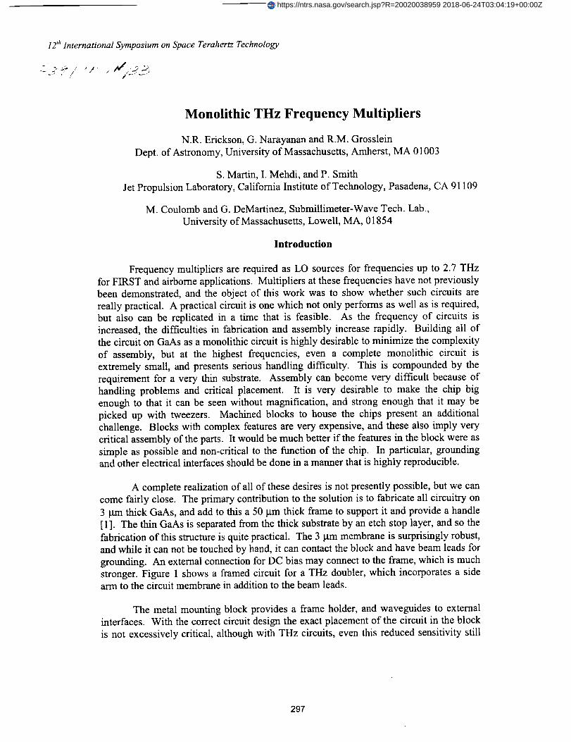
12_hInternational Symposium on Space Teraher= Technology
Monolithic THz Frequency Multipliers
N.R. Erickson, G. Narayanan and R.M. Grosslein
Dept. of Astronomy, University of Massachusetts, Amherst, MA 01003
S. Martin, I. Mehdi, and P. Smith
Jet Propulsion Laboratory, California Institute of Technology, Pasadena, CA 91109
M. Coulomb and G. DeMartinez, Submillimeter-Wave Tech. Lab.,
University of Massachusetts, Lowell, MA, 01854
Introduction
Frequency multipliers are required as LO sources for frequencies up to 2.7 THz
for FIRST and airborne applications. Multipliers at these frequencies have not previously
been demonstrated, and the object of this work was to show whether such circuits are
really practical. A practical circuit is one which not only performs as well as is required,
but also can be replicated in a time that is feasible. As the frequency of circuits isincreased, the difficulties in fabrication and assembly increase rapidly. Building all of
the circuit on GaAs as a monolithic circuit is highly desirable to minimize the complexity
of assembly, but at the highest frequencies, even a complete monolithic circuit is
extremely small, and presents serious handling difficulty. This is compounded by the
requirement for a very thin substrate. Assembly can become very difficult because of
handling problems and critical placement. It is very desirable to make the chip big
enough to that it can be seen without magnification, and strong enough that it may be
picked up with tweezers. Machined blocks to house the chips present an additionalchallenge. Blocks with complex features are very expensive, and these also imply very
critical assembly of the parts. It would be much better if the features in the block were as
simple as possible and non-critical to the function of the chip. In particular, groundingand other electrical interfaces should be done in a manner that is highly reproducible.
A complete realization of all of these desires is not presently possible, but we cancome fairly close. The primary contribution to the solution is to fabricate all circuitry on
3 _un thick GaAs, and add to this a 50 lain thick frame to support it and provide a handle
[ 1]. The thin GaAs is separated from the thick substrate by an etch stop layer, and so the
fabrication of this structure is quite practical. The 3 lain membrane is surprisingly robust,and while it can not be touched by hand, it can contact the block and have beam leads for
grounding. An external connection for DC bias may connect to the frame, which is much
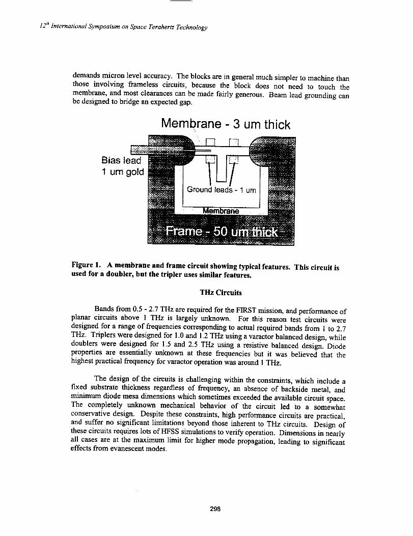
stronger. Figure 1 shows a framed circuit for a THz doubler, which incorporates a sidearm to the circuit membrane in addition to the beam leads.
The metal mounting block provides a frame holder, and waveguides to externalinterfaces. With the correct circuit design the exact placement of the circuit in the block
is not excessively critical, although with THz circuits, even this reduced sensitivity still
297
https://ntrs.nasa.gov/search.jsp?R=20020038959 2018-06-24T03:04:19+00:00Z
12_ International Symposium on Space Terahertz Technology
demands micron level accuracy. The blocks are in general much simpler to machine than
those involving frameless circuits, because the block does not need to touch the
membrane, and most clearances can be made fairly generous. Beam lead grounding can
be designed to bridge an expected gap.
Membrane- 3 um thick
Bias lead
1 um gold
Figure 1. A membrane and frame circuit showing typical features. This circuit is
used for a doubler, but the tripler uses similar features.
THz Circuits
Bands from 0.5 - 2.7 THz are required for the FIRST mission, and performance of
planar circuits above 1 THz is largely unknown. For this reason test circuits were
designed for a range of frequencies corresponding to actual required bands from 1 to 2.7THz. Triplers were designed for 1.0 and 1.2 THz using a varactor balanced design, while
doublers were designed for 1.5 and 2.5 THz using a resistive balanced design. Diode
properties are essentially unknown at these frequencies but it was believed that the
highest practical frequency for varactor operation was around 1 THz.
The design of the circuits is challenging within the constraints, which include afLxed substrate thickness regardless of frequency, an absence of backside metal, and
minimum diode mesa dimensions which sometimes exceeded the available circuit space.
The completely unknown mechanical behavior of the circuit led to a somewhat
conservative design. Despite these constraints, high performance circuits are practical,and suffer no significant limitations beyond those inherent to THz circuits. Design of
these circuits requires lots of HFSS simulations to verify operation. Dimensions in nearly
all cases are at the maximum limit for higher mode propagation, leading to significanteffects from evanescent modes.
298

12 'h International Symposium on Space Terahertz Technology
Doubler Design
At frequencies near 2 THz, carrier velocity saturation effects seriously limit
varactor operation. An approximate value for the peak junction current, estimated from
the carrier concentration in the junction, times the maximum saturated carrier velocity, is
3 mA/fF. At 1 THz, a sinusoidal wave has only a 1 V peak-peak amplitude at this
current. This means little voltage modulation is possible, and varactor efficiency will be
very low. Resistive multiplication requires lower voltage amplitude, and still should
work with reasonable efficiency, although it is inherently less efficient. These circuits
are required to produce only a few microwatts of output power to drive HEB mixers, and
the input power is likely to be very limited as well. Little data is available on multipliers
above 700 GHz, and those that have been built have not been intended to produce high
power. Projections of optimized drive levels are in the 0.25 to 1 mW level at most. At
low power, simulations show that DC forward bias is essential for best efficiency, and
zero bias is favored only for power levels far higher than would be available. A balanced
design was chosen because it requires no filters, and is very simple, despite the fact that it
uses two diodes which double the required input power. Losses in filters can easily
exceed the penalty for using two diodes. For the 2.5 THz design, diodes with Cj(0) = 0.5
fF were chosen to minimize the required input power. Even smaller diodes seemed
desirable but were too far outside the known range for planar diode fabrication. For 1.5
THz, diodes may be significantly larger, at 0.9 fF, and circuit design is easier, because
these diodes more closely match the typical circuit impedance levels. Figure 2 shows the
predicted efficiency vs. power for a 1.5 THz doubler.
t--
.o
iii
0.020
0.015
0.010
0.005
0 ¸
0
1.5 THz doubler, CI(O)=0.9 fF, R B= 110_1
!!1 2 3 4 5
Input Power (mW)
Figure 2. Predicted efficiency vs. input power for a doubler to 1.5 THz using a pair of diodes with
Cj(0) = 0.9 fF and R_ = 110_, biased in the forward direction.
299
12 'hInternational Symposium on Space Terahertz Technology
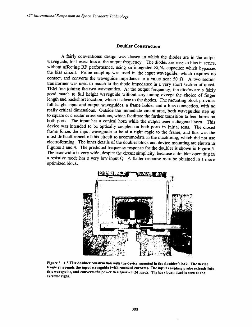
Doubler Construction
A fairly conventional design was chosen in which the diodes are in the outputwaveguide, for lowest loss at the output frequency. The diodes are easy to bias in series,
without affecting RF performance, using an integrated Si3N4 capacitor which bypassesthe bias circuit. Probe coupling was used in the input waveguide, which requires no
contact, and converts the waveguide impedance to a value near 50 f2. A two section
transformer was used to match to the diode impedance in a very short section of quasi-TEM line joining the two waveguides. At the output frequency, the diodes are a fairly
good match to full height waveguide without any tuning except the choice of finger
length and backshort location, which is close to the diodes. The mounting block providesfull height input and output waveguides, a frame holder and a bias connection, with no
really critical dimensions. Outside the immediate circuit area, both waveguides step upto square or circular cross sections, which facilitate the further transition to feed homs on
both ports. The input has a conical horn while the output uses a diagonal horn. This
device was intended to be optically coupled on both ports in initial tests. The closed
frame forces the input waveguide to be at a right angle to the frame, and this was the
most difficult aspect of this circuit to accommodate in the machining, which did not use
electroforming. The inner details of the doubler block and device mounting are shown in
Figures 3 and 4. The predicted frequency response for the doubler is shown in Figure 5.
The bandwidth is very wide, despite the circuit simplicity, because a doubler operating ina resistive mode has a very low input Q. A flatter response may be obtained in a moreoptimized block.
Figure 3. 1.5 THz doubler construction with the device mounted in the doubler block. The deviceframe surrounds the input waveguide (with rounded corners). The input coupling probe extends intothis waveguide, and converts the power to a quasi-TEM mode. The bias beam lead is seen to theextreme right.
300

12 'h International Symposium on Space Terahertz Technology
Figure 4. 1.5 THz doubler detail showing the connection of the input probe to the center pointbetween the diodes, which are mounted in the output waveguide. There are four grounding beamleads. The right hand ground includes an integrated SiN capacitor to bypass the bias line.
1:
0,0'0.8
0.7
0.5
0.3
0.2
0.1'-
1_'.2 113 114 1.5 1.6 1,7
FrEK:lUancy (THz)
Figure 5. 1.5 THz doubler predicted efficiency vs. frequency at 2 mW input.
Devices
All of the devices were fabricated at JPL on a pair of nominally identical wafers,
which included many other designs. The wafer is undoped GaAs having a final thickness
of about 50 Bin, with an epi structure (grown by MOCVD by Epitronics) as shown in
Table 1.Mat'l Thickness
Epi layer GaAs 0.15 bun
N++ layer GaAs 1.0 }trn
Etch stop Gao.sAl05As 0.05 }trn
Membrane GaAs 3.0 _rn
Etch stop Ga0.sA10.sAs 0.4 }axn
Dopin[_5.0 x 1017 Si
5.0 x 10 Is Si
undoped<3 x 10 TM
undoped
Table 1
301
12'h International Symposium on Space Terahertz Technology
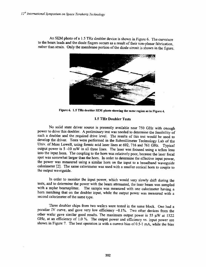
An SEM photo of a 1.5 THz doubler device is shown in Figure 6. The curvature
to the beam leads and the diode f'mgers occurs as a result of their non-planar fabrication,
rather than strain. Only the membrane portion of the diode circuit is shown in the figure.
Figure 6. 1.5 THz doubler SEM photo showing the same region as in Figure 4.
1.5 THz Doubler Tests
No solid state driver source is presently available near 750 GHz with enoughpower to drive this doubler. A preliminary test was needed to determine the feasibility of
such a doubler and the required drive level. The results of this test would be used to
develop the driver. Tests were performed in the Submillimeter Technology Lab of the
Univ. of Mass Lowell, using formic acid laser lines at 692, 716 and 761 GHz. Typical
output power is 5 -10 mW in all three lines. The laser was focused using a teflon lens
into the input horn. The coupling to the horn was relatively poor, because the laser focal
spot was somewhat larger than the horn. In order to determine the effective input power,
the power was measured using a similar horn on the input to a broadband waveguide
calorimeter [2]. The same calorimeter was used with a smaller conical horn to couple tothe output waveguide.
In order to monitor the input power, which would very slowly drift during the
tests, and to determine the power with the beam attenuated, the laser beam was sampledwith a mylar beamsplitter. The sample was measured with one calorimeter having a
horn matching that on the doubler input, while the output power was measured with a
second calorimeter of the same type.
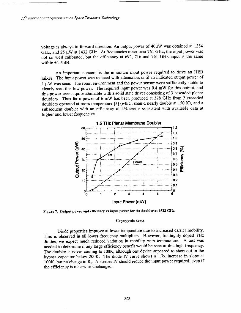
Three doubler chips from two wafers were tested in the same block. One had a
peculiar IV curve, and gave very low efficiency --_.1%. Two other devices from the
other wafer gave similar good results. The maximum output power is 55 [.tW at 1522
GHz, at an efficiency of 1.0 %. The output power and efficiency vs. input power are
shown in Figure 7. The best operation is with a current bias of 0.5-1 mA, while the bias
302
12 'h International Symposium on Space Terahertz Technology
voltage is always in forward direction. An output power of 40gW was obtained at 1384
GHz, and 25 gW at 1432 GHz. At frequencies other than 761 GHz, the input power was
not so well calibrated, but the efficiency at 692, 716 and 761 GHz input is the same
within +1.5 dB.
An important concern is the minimum input power required to drive an HEB
mixer. The input power was reduced with attenuators until an indicated output power of
1 gW was seen. The room environment and the power sensor were sufficiently stable to
clearly read this low power. The required input power was 0.4 mW for this output, and
this power seems quite attainable with a solid state driver consisting of 3 cascaded planar
doublers. Thus far a power of 6 mW has been produced at 378 GHz from 2 cascaded
doublers operated at room temperature [3] (which should nearly double at 150 K), and a
subsequent doubler with an efficiency of 4% seems consistent with available data at
higher and lower frequencies.
1.5 THz Planar Membrane Doubler
I ............. i ............ _ ........... 4 ............ _ ................ _ ................... i ............ _...........-----_-4 ............ :--- : ...........50
...........i........ ................i...........o, ........ "ili:::ilZ:i:::ili ill .......
....../! .............i..... ...............i...........20-...._ .......... _..........
" i -_ ........... ;............ t ............ :...........: ..... ',.......... ."............. i ........... .'.............10
...... i¢,'_............ _........... _............ i........... i..........0 _'.. i . . . i . . . I . , , _ . . . _ . • •0 1 2 3 4 5
Input Power (mW)
1.2
1.1
1.0
0.9
0.8 g
0.7 o>,
0.6 _)0.5 "_
o.4 wuJ
0.3
0.2
0.1
06
Figure 7. Output power and efficiency vs input power for the doubler at 1522 GHz.
Cryogenic tests
Diode properties improve at lower temperature due to increased cartier mobility.
This is observed in all lower frequency multipliers. However, for highly doped THz
diodes, we expect much reduced variation in mobility with temperature. A test was
needed to determine if any large efficiency benefit would be seen at this high frequency.
The doubler survives cooling to 100K, although one device appeared to short out in the
bypass capacitor below 200K. The diode IV curve shows a 1.7x increase in slope at
100K, but no change in Rs. A steeper IV should reduce the input power required, even if
the efficiency is otherwise unchanged.
303

12'j' International Symposium on Space Terahertz Technology
A fairly crude test was done with the doubler tested over a LN2 bath with the laser
input at 2.5 roW. At a temperature of 230K the output increased -10%, but at lower
temperature frost began to build up on the input horn, and the output power showed no
further increase, with an actual decrease below 180K. A proper test would require a realdewar, but this test suggests that no major efficiency improvement will occur, since the
frost build up did not appear to be sufficiently large to produce a very large loss.
Machining
The machining of the block was very easy, considering the small sizes involved.
The small features were machined with a 50 larn diameter end mill on a micro-milling
machine [4], while the larger features used a 150 ixrn diameter mill in a second spindle.
All critical features used the smaller mill so registration of the tools was not a problem.
The one difficult feature was the right angle waveguide, which required plunging aconical horn through a thick block and then meeting this feature with a milled cut from
the opposite side. It would be much simpler to machine if this waveguide could be
rotated into the same plane as other features, so that both waveguides are split in the E-
plane.
The input waveguide can not cross the frame because the presence of the GaAs in
the waveguide produces a very large mismatch. However, the frame can be removed. In
a test, the frame was glued down at the comers and the frame was then broken in the
required area without damage to the membrane. Rotating the input waveguide 90 ° has no
effect on the input match, and the required backshort location fits within the remaining
frame. The doubler for 2.5 THz will be machined this way, greatly simplifying thissmaller and more difficult part, and also will be tested with a laser.
1 THz Tripler
The 1.0 and 1.2 THz triplers are based on a successful monolithic tripler tested in
the 230-330 GHz range [5]. The change is mostly just a scaling in size, but the
membrane is significantly thinner than the scaled substrate thickness for the 300 GHz
version. The circuit includes two antiparallel diodes in a loop with nearly optimized
second harmonic inductance, having an integrated Si3N4 capacitor for DC bias bypass.Beam leads are used for dc and rfgrounding, and two radial stubs are used to prevent loss
of output power to the input circuit. In this smaller size there is some considerable doubtabout the effective dielectric constant for radial stubs on the GaAs membrane which
depend on the metal of the block for a ground plane. The design assumed that there
would be a 1 Ixm gap under the GaAs, and the stubs were sized accordingly. Variation in
this gap is not too critical, and it is unlikely to exceed 2 _tm in the worst case. Surface
roughness insures that it will never drop below 0.5 l.tm. An input waveguide probe wasadded to the THz models to fully integrate the circuit. Because the input probe dominates
304
12 _hInternational Symposium on Space Terahertz Technology
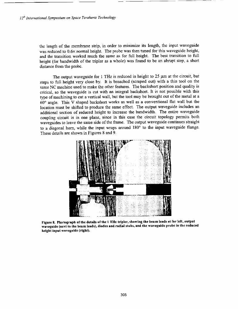
the length of the membrane strip, in order to minimize its length, the input waveguide
was reduced to 0.6x normal height. The probe was then tuned for this waveguide height,and the transition worked much the same as for full height. The best transition to full
height (for bandwidth of the tripler as a whole) was found to be an abrupt step, a short
distance from the probe.
The output waveguide for 1 THz is reduced in height to 25 I.tm at the circuit, but
steps to full height very close by. It is broached (scraped out) with a thin tool on thesame NC machine used to make the other features. The backshort position and quality is
critical, so the waveguide is cut with an integral backshort. It is not possible with this
type of machining to cut a vertical wall, but the tool may be brought out of the metal at a
60 ° angle. This V shaped backshort works as well as a conventional flat wall but the
location must be shifted to produce the same effect. The output waveguide includes anadditional section of reduced height to increase the bandwidth. The entire waveguide
coupling circuit is in one plane, since in this case the circuit topology permits both
waveguides to leave the same side of the frame. The output waveguide continues straight
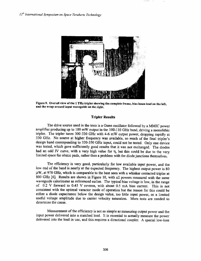
to a diagonal horn, while the input wraps around 180 ° to the input waveguide flange.These details are shown in Figures 8 and 9.
Figure 8. Photograph of the details of the 1 THz tripler, showing the bea m leads at far left, outputwaveguide (next to the beam leads), diodes and radial stubs, and the waveguide probe in the reducedheight input waveguide (right).
305
lh • .
12 Internatlonal Sympostum on Space Terahertz Technology
Figure 9. Over all view of the 1 THz tripler showing the complete fra me, bias beam lead on the left,and the wrap-around input waveguide on the right.
Tripler Results
The drive source used in the tests is a Gurm oscillator followed by a MMIC poweramplifier producing up to 100 mW output in the 100-110 GHz band, driving a monolithic
tripler. The tripler tunes 300-330 GHz with 4-6 mW output power, dropping rapidly at
330 GHz. No source at higher frequency was available, so much of the fmal tripler'sdesign band corresponding to 320-350 GHz input, could not be tested. Only one device
was tested, which gave sufficiently good results that it was not exchanged. The diodes
had an odd IV curve, with a very high value for rl, but this could be due to the very
limited space for ohmic pads, rather than a problem with the diode junctions themselves.
The efficiency is very good, particularly for low available input power, and the
low end of the band is nearly at the expected frequency. The highest output power is 80
_tW, at 978 GHz, which is comparable to the best seen with a whisker contacted tripler at800 GHz [6]. Results are shown in Figure 10, with all powers measured with the same
waveguide calorimeter as referenced earlier. The typical bias voltage is low, in the rangeof 0.2 V forward to 0.45 V reverse, with about 0.5 mA bias current. This is not
consistent with the optimal vamctor mode of operation but the reason for this could be
either a diode capacitance below the design value, too little input power, or a limiteduseful voltage amplitude due to carrier velocity saturation. More tests are needed todetermine the cause.
Measurement of the efficiency is not so simple as measuring output power and the
input power delivered into a matched load. It is essential to actually measure the powerdelivered into the load in use, and this requires a directional coupler. A special low-loss
306

12 'h International Symposium on Space Terahertz Technology
high-directivity WR3 coupler was built for this work [7]. In these tests the true efficiency
was measured to be 0.8-1.1% in the 965-980 GHz range, with input powers --4 mW. No
rapid change with input power was noted, although this power should be too low for best
efficiency. The input reflected power was 10-20%.
Operation of the full chain, shown in Figure 11, is extremely simple. There are no
tuners on the multipliers, and their only adjustment is the bias level. The input frequency
is set with Gunn tuner and power with the voltage bias on the power amp. This makes
the chain fully compatible with space or remote operation. The interaction between
driver multiplier and THz tripler is acceptable, in that any input frequency may be chosen
without seeing large output power variations. However, the band tested so far is quite
limited relative to that required for FIRST, and full tests are planned when the actual
driver chain (consisting of two cascaded doublers) is completed. At low temperature,
much higher output power is expected, because the driver tripler is known to show a 57%
increase in power [5], and the final tripler should show at least some improvement.
_oof .
9oI80
6O
500-
40
20
10
............................ !10
19
.... :np_ __,,,powEr _.__. ,...._. r i6 E
f 'l _'j _, "_--. at 4 mW input _
£
940 960 980 1000 1020 1040 1060 1080
Output Frequency (GHz)
Figure I0. Input power (delivered to a matched load), and output power for the I THz tripler, aswell as the predicted output power with 4 mW input. Actual input differs due to interactions. Nosource was available above 330 GHz.
307

12 'h International Symposium on Space Terahertz Technology
Figure 11. Photo of the complete 1 THz multiplier chain, consisting of (left to right) 100-110 GHz
power amp, 320 GHz tripler and 1 THz tripler. The output waveguide on the tripler is a transitionfrom circular to WR10, to match to the power sensor.
Conclusions
The results of this work show that THz monolithic frequency multipliers are quitepractical, with excellent performance. A very limited data set indicates that they are also
reproducible. These results now make whiskered devices obsolete at all frequencies. At
all lower frequencies, planar devices have already shown their superiority, particularlywhen integrated with most of the multiplier circuitry. The requirement to achieve such
good performance is that the circuit must be simple, and there must be an absolute
minimum of microstrip or other planar transmission line circuitry. Any such circuitrymust be used with careful attention to the losses that will be produced.
The efficiency is high enough to make practical THz solid state sources, which
only need to produce a few ktW in order to drive SIS or HEB mixers. Cascaded sources
are possible with little power ripple vs. frequency, although this may apply only overlimited bandwidths. Membrane circuits are quite fragile, yet are quite robust in actual use
since they never need to be subjected to significant strain. Machining of the blocks isquick and easy relative to any previous designs, requiring nearly a factor of ten less time
than is needed for a whiskered device at the same frequency. Assembly is remarkably
easy for such high frequency, and a block may be taken from machined parts to fullyfunctional in a time of-4 hours.
The large (3 inch) wafer size means that many devices are available, even with a
low yield, and a single wafer may contain 10's of different designs, with 100's of each
design. This meets the requirements for a major space mission such as FIRST, and also
enables a very wide range of other uses. While a wafer run is quite expensive, this
308

12'h International Symposium on Space Terahertz Technology
enormous productivity makes circuits in the THz region quite affordable, relative to their
whiskered equivalents, and the long term reliability is certain to be much better as well.
References
[1] P.H. Seigel, R.P. Smith, S. Martin, and M. Gaidis, "2.5 THz GaAs MonolithicMembrane-Diode Mixer," IEEE Trans. Microwave Theory Tech., v. 47, pp. 596-604,
May 1999.
[2] N. Erickson, "A Fast and Sensitive Submillimeter Waveguide Power Meter," Tenth
International Symposium on Space Terahertz Technology, pp. 501-507, Mar. 99.
[3] E. Schlecht, J. Bruston, A. Maestrini, S. Martin, D. Pukala, R. Tsang, R.P. Smith, and
I. Mehdi, "200 and 400 GHz Schottky Diode Multipliers Fabricated with Integrated Air-
dielectric "'Substrateless" Circuitry," Eleventh International Symposium on Space
Terahertz Technology, pp. 287-295, May 2000.
[4] G. Narayanan, N. Erickson, and R. Grosslein, "Low Cost Direct Machining ofTerahertz waveguide Structures," Tenth International Symposium on Space Terahertz
Technology, pp. 518-528, Mar. 99.
[5] N. Erickson, R. Smith, and S. Martin, "High Efficiency MMIC Frequency Triplers
for Millimeter and Submillimeter Wavelengths," IEEE MTT-S lnt7 Microwave
Symposium, June 2000, Boston.
[6] N.R. Erickson, and J. Tuovinen, "'A Waveguide Tripler for 720-880 GHz," Sixth lnt'l
Symposium on Space Terahertz Tech., pp. 191-198, 1995.
[7] N.R. Erickson, "High Performance Dual Directional Couplers for Near-mm
Wavelengths," to be published in IEEE Microwave and Guided Wave Lett, 2001
Part of the research described in this paper was carried out at the Jet Propulsion Laboratory, CaliforniaInstitute of Technology, under a contract with the National Aeronautics and Space Administration.
309