Embed Size (px)
Citation preview
Monolithically integrated dual-channel coherentreceiver with widely tunable local oscillator for100 Gbps dual-polarization quadrature phaseshift keying applicationsPHILLIP J. SKAHAN,1,* SARAT GUNDAVARAPU,1 KIMCHAU N. NGUYEN,2 DOUGLAS M. BANEY,3 AND
DANIEL J. BLUMENTHAL1
1Electrical and Computer Engineering Department, University of California, Santa Barbara, California 93106, USA2Intel Corporation, 2200 Mission College Blvd., SC-12, MS 326, Santa Clara, California 95054, USA3Keysight Laboratories, Keysight Technologies, 5301 Stevens Creek Blvd., Santa Clara, California 95051, USA*Corresponding author: [email protected]
Received 13 May 2015; revised 22 August 2015; accepted 22 August 2015; posted 24 August 2015 (Doc. ID 239933); published 11 September 2015
We report implementation of a monolithically integrated100 Gbps dual-polarization quadrature phase shift keying(DP-QPSK) wavelength tunable coherent receiver on a1 mm × 3 mm die that consists of a tunable C-Band localoscillator with a 40 nm range, eight 30 GHz photodetectors,and two parallel 90° optical hybrids. A BER of 10−3 with anOSNR of 7.5 dB operating at 50 Gbps NRZ-QPSK data perchannel is reported. © 2015 Optical Society of America
OCIS codes: (060.2330) Fiber optics communications; (060.1660)
Coherent communications; (130.3120) Integrated optics devices.
http://dx.doi.org/10.1364/OL.40.004313
Coherent data transmission is used to increase the spectralefficiency of existing fiber optic transmission systems and im-prove tolerance to transmission impairments. As the industrymoves toward reducing transceiver costs to below $1/Gb,monolithic integration of the system components is beneficialfor cost, size, and power reduction, especially considering theincreased component count and complexity of the transmittersand receivers required for higher-order modulation formats. Inthe case of the receiver, there are strict tolerances on insertionlosses, optical and electrical signal-to-noise ratio, and receivedsignal phase control. Differences in the quadrature angle ofthe incoming signal phase at the photodetectors will result inreceived signal degradation and an increased bit error rate. Byintegrating all optical paths on-chip, path length differencesmay be tightly controlled and phase error minimized. On-chipintegration of the local oscillator (LO) also minimizes opticalloss, thus reducing power requirements on the tunable lasersand resulting in improved link sensitivity, reduced physicalfootprint, and reduced system complexity.
Demonstrations of monolithic coherent receivers on InP todate include on- or off-chip polarization splitters and rotators,90° optical hybrids, and balanced photodetectors [1–7]. These
designs use an external laser source as the LO. Another examplehas implemented an array of static distributed feedback lasersand receivers for wavelength division multiplexing applications[8]. One recent example implemented a second regrowth tointegrate both the LO and high-speed photodetectors, at thecost of increased process complexity [9]. Two receiver examplesintegrate an LO with a single- or dual-channel coherent receiverbut were RC limited by parasitic capacitance in the photodetec-tor electrical pads and did not come close to utilizing availableperformance in the quantum-well diodes [10,11].
The monolithically integrated receiver reported here utilizesan improved photodiode contact design, which consists of athicker low-κ dielectric material beneath the contacts and re-duced contact surface area. This results in photodiodes limitedby electron transit time through the absorption layer ratherthan the external RF path. These contacts have remainedcapable of wire bonding and showed an improved 3 dB RFresponse of over 30 GHz, including wire bond and coplanartransmission line network. A single on-chip LO signal split be-tween the two channels reduces system complexity and cost,and the fabrication process requires only a single regrowth stepto define the quantum wells used for gain and absorption.
A system-level schematic of the receiver is shown inFig. 1(a). The receiver consists of two parallel 90° opticalhybrids, eight single-ended photodetectors, a sampled-gratingdistributed Bragg reflector (SG-DBR) laser, and connectingwaveguides. The hybrids consist of four four-port multimodeinterferometer (MMI) splitters designed to split the incomingoptical signal 50/50 into each output port, similar to [12]. TheMMIs were designed to operate over a 100 nm range from1500 to 1600 nm. The first set of MMIs split the data andLO signals, and one output port from each MMI is routedto each of the second set of MMIs, which mix the data andLO signal; the unused input ports on the hybrids were termi-nated with absorbing regions to minimize reflections. The LOpath to the lower MMI is tuned 90° out of phase with respect to
Letter Vol. 40, No. 18 / September 15 2015 / Optics Letters 4313
0146-9592/15/184313-04$15/0$15.00 © 2015 Optical Society of America
the upper LO path using an electro-optic phase shifter, thusproducing the quadrature data. The optical signals are thendetected in waveguide photodiodes downstream of the MMIoutputs; the diodes are single-ended due to a shared n-type sub-strate ground. The SG-DBR laser consists of a front mirror,back mirror, and phase section with electro-optic phase shifters,a gain section, and an absorber section. The laser is designedwith a Bragg wavelength λB � 1540 nm, and the peak spacingis 3.55 and 3.24 nm for the front and back mirrors, respec-tively. The output of the laser is TE-polarized due to tensilestrain on the quantum wells in the gain section. The LO outputis split by a 1 × 2 MMI and routed to each optical hybrid. Aphotograph of the fabricated device is shown in Fig. 1(b).
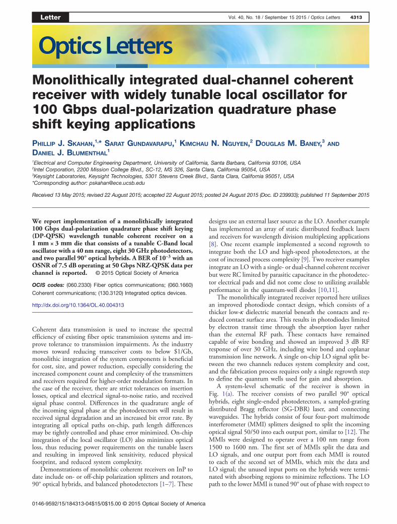
The receiver was fabricated on a semiconducting InP sub-strate. The epitaxial structure consists of a quaternary waveguidelayer with a 1.4 μm bandgap, a multiple quantum well gain/absorption layer, and a regrown InP upper cladding. The fabri-cation process consists of eight mask layers and one regrowth.All features except the waveguide gratings were defined usingan i-line stepper; the gratings were defined using electron beamlithography. Novel steps in the device fabrication include use ofbenzocyclobutene (BCB) under the metal contacts of the photo-detectors, reduced photodiode contact surface area, and an in-ductively coupled plasma (ICP) dry etch for the waveguides. Aschematic of the fabricated photodetector is shown in Fig. 2. Thephotosensitive BCB was spun at low revolutions per minute, re-sulting in a 7.5 μm thick layer after curing. The metal contactswere defined 14 μm around the waveguides with a 60 μm diam-eter circular pad at one end for wire bonding; total pad surfacearea is ∼4000 μm2. Waveguides were etched into the semicon-ductor material with an ICP dry etch consisting of chlorine,nitrogen, and argon gas. Line edge roughness of the resultingwaveguides was measured to be 20 nm root mean square, whichis sufficient for propagation losses lower than 2 dB/mm. Thefabricated device was thinned to 150 μm, cleaved, and solderedto an AlN carrier for improved thermal stability.
The LO was first tested to determine the range of operation,output power, and side mode suppression ratio (SMSR).Tuning range was determined by sweeping the front and back
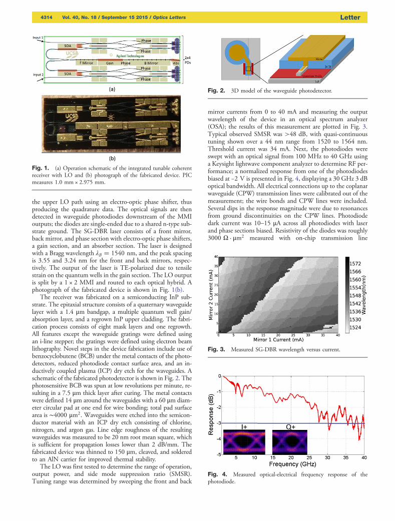
mirror currents from 0 to 40 mA and measuring the outputwavelength of the device in an optical spectrum analyzer(OSA); the results of this measurement are plotted in Fig. 3.Typical observed SMSR was >48 dB, with quasi-continuoustuning shown over a 44 nm range from 1520 to 1564 nm.Threshold current was 34 mA. Next, the photodiodes wereswept with an optical signal from 100 MHz to 40 GHz usinga Keysight lightwave component analyzer to determine RF per-formance; a normalized response from one of the photodiodesbiased at −2 V is presented in Fig. 4, displaying a 30 GHz 3 dBoptical bandwidth. All electrical connections up to the coplanarwaveguide (CPW) transmission lines were calibrated out of themeasurement; the wire bonds and CPW lines were included.Several dips in the response magnitude were due to resonancesfrom ground discontinuities on the CPW lines. Photodiodedark current was 10–15 μA across all photodiodes with laserand phase sections biased. Resistivity of the diodes was roughly3000 Ω · μm2 measured with on-chip transmission line
Fig. 1. (a) Operation schematic of the integrated tunable coherentreceiver with LO and (b) photograph of the fabricated device. PICmeasures 1.0 mm × 2.975 mm.
Fig. 3. Measured SG-DBR wavelength versus current.
Fig. 2. 3D model of the waveguide photodetector.
Fig. 4. Measured optical-electrical frequency response of thephotodiode.
4314 Vol. 40, No. 18 / September 15 2015 / Optics Letters Letter

method structures; this resulted in the 30 × 3.65 μm photodi-odes typically having a resistance of about 27 Ω. Responsivityof the photodiode was 0.3 A/W measured with an off-chip teststructure; the measurement includes coupling loss from alensed fiber with a 2.5 μm spot size to the on-chip waveguide.Net receiver responsivity was measured and is plotted versuswavelength in Fig. 5 for a −1.5 V bias on the photodiodes;the maximum net responsivity was 0.03 A/W at 1513 nm.Useful optical bandwidth of the receiver is over 100 nm. Netresponsivity includes 6 dB splitting loss in the hybrid and theresponsivity of the photodiodes; thus, the excess loss of thereceiver is 4.1 dB or roughly 1.4 dB/mm waveguide loss dueto photon scattering from line edge roughness and inter-valenceband absorption in the upper cladding layer.
To verify photodiode operation, an amplitude-shift keyednonreturn-to-zero (NRZ) pseudorandom binary sequence(PRBS) with a pattern length of 27 − 1 at 25 GHz was fed intothe device and recovered at the positive in-phase (I�) andquadrature (Q�) photodiodes. The optical signal was preampli-fied to 20 dBm using an erbium-doped fiber amplifier (EDFA)and filtered using a 0.4 nm tunable filter before being coupledinto the chip, and the received photocurrent was amplified withan RF amplifier, similar to the setup shown in Fig. 6. Open eyesfrom both photodiodes are shown as inserts in Fig. 4.
The available LO power was determined by biasing the laserat 191 mA and measuring the photocurrent in the diodes;the LO photocurrents were in the range of 200–300 μA acrossthe photodiodes. The linewidth of the LO was then measuredusing the self-heterodyne method. The output from the back ofthe LO was coupled off-chip using a lensed fiber and then splitin a 50/50 fiber coupler. One output was delayed with a20 km length of LEAF fiber, and the other output was shifted100 MHz using an acousto-optic modulator. The beams werethen combined in another 50/50 fiber coupler, converted to anelectrical current through a high-speed photodiode, and mea-sured in an electrical spectrum analyzer with a 200 kHz reso-lution bandwidth. Linewidths (3 dB) of 12, 15, and 18 MHzwere measured at 1545.26, 1548.38, and 1551.5 nm, respec-tively; these wavelengths were achieved by tuning only the frontmirror of the laser. The increasing trend in linewidth is likelydue to increased electro-optic absorption in the mirrors, as eachhigher wavelength required a 2–3 mA increase in the current tothe front mirror. To eliminate reflections from the back facet,which could cause injection locking of the SG-DBR, theabsorber section of the laser was reverse biased. At the front
of the laser, reflections from the hybrids back into the LO wereminimal due to 8 dB of path loss through the waveguide bends,resulting in 16 dB total return loss. An external cavity laser witha 100 kHz linewidth was coupled with the on-chip LO usingthe on-chip hybrid, and the RF spectrum of the resulting beatfrequency was measured from one of the photodiodes. The3 dB linewidth of the beat tone was 130 MHz, which is muchlarger than the linewidth of the individual lasers, due to signifi-cant 1/f noise of the two lasers from thermal fluctuations andvibrations. The beat frequencies detected in the I� and Q�photodetectors were then viewed simultaneously with a real-timeoscilloscope, and the phase path of the lower half of each hybridwas tuned so that the beat frequencies were 90° out of phase,thus ensuring quadrature encoded data recovery. A 50 GbpsNRZ quadrature phase-shift keyed (QPSK) signal generatedfrom two individual PRBS 27 − 1 data streams was used to testindividual channel operation; the test setup is shown in Fig. 6.
A polarizing beam splitter cube was used before the receiverinputs to separate incoming polarization-multiplexed signals;the transverse-electric (TE) path was fed directly to one chan-nel, while the transverse magnetic (TM) signal was rotated tothe TE orientation using a polarization controller before beingfed to the other channel for compatibility with the LO signal.The optical signal was again preamplified to 20 dBm using anEDFA and filtered with a 0.4 nm tunable filter before beingcoupled into the chip, and the received photocurrents were am-plified with an RF amplifier and processed using a Keysightoptical modulation analyzer (OMA). The OMA contains adigital signal processor (DSP), which performed equalization,clock recovery, carrier phase estimation, decoding, and errordetection. Three different wavelengths were tested to verifyreceiver operation, and the resulting bit-error rate (BER) versusthe optical signal-to-noise ratio (OSNR) of the input signal ispresented in Fig. 7.
An error floor was measured at 10−8 for all three wave-lengths, likely due to the 130 MHz linewidth of the beat tone.A BER of 10−3 was achieved at an OSNR of 7.5 dB for the1548.38 and 1551.5 nm wavelengths, while an OSNR of11.5 dB was required to achieve the same BER at 1545.26 nm.This difference can be attributed to the carrier phase estimationalgorithm implemented in the DSP, which uses a Kalman filterto compensate for the phase noise of the beat tone and deter-mine the phase of the signal. At 1545.26 nm, the LO linewidthwas narrow enough that the phase estimation could be set low,resulting in less phase distortion of the recovered signal, asshown in the recovered constellation in Fig. 8. At 1548.38and 1551.5 nm, the linewidths required more aggressive phaseestimation, resulting in increased phase distortion of the recov-ered constellations. A secondary effect was an improvement inthe measured BER versus OSNR at these wavelengths, as thephase estimation likely caused minor error correction of someof the errors from noise in the incoming signal, resulting in ameasured BER exceeding the theoretical limit for a nonerror-corrected signal at the lower OSNR points.
Fig. 5. Measured net receiver responsivity versus wavelength.
Fig. 6. Schematic of the setup used for receiver characterization.
Letter Vol. 40, No. 18 / September 15 2015 / Optics Letters 4315

In conclusion, we demonstrated a monolithically integrateddual-channel heterodyne receiver with a widely tunable localoscillator for application in 100 Gbps optical networks utilizingcoherent modulation formats. The receiver consists of a tunableC-band local oscillator with a 40 nm range, eight 30 GHz pho-todetectors, and two parallel 90° optical hybrids integrated on a1 mm × 3 mm die. We found that the improved photodiodedesign consisting of a thicker low-κ dielectric material beneaththe contacts and a reduced contact surface area resulted in de-vices limited by electron transit time through the absorptionlayer rather than the external RF path. The contacts for thesedevices remained capable of wire bonding and showed an im-proved 3 dB response of over 30 GHz, including the wire bondand coplanar transmission line network. Only a single regrowthstep was required to define the quantum wells used for gain andabsorption, minimizing process complexity. The on-chip LOsignal split between the two channels resulted in reduced sys-tem complexity, cost, and improved link sensitivity with no ob-served instability due to on-chip reflections, which is likely dueto 16 dB return loss through the LO output path. We measuredan LO linewidth of 12–18 MHz at three different wavelengthsand found that the linewidth was correlated to current injectionof the tuning mirror. Using 50 Gbps NRZ-QPSK data perchannel, we demonstrated a BER of 10−3 at an OSNR of7.5 dB at three different wavelengths, and we observed anerror floor at a BER of 10−8 caused by the 130 MHz linewidthof the beat tone. Future directions for this work include line-width reduction of the LO and optical phase locking to enablehigher-modulation formats. Thermally tuned SG-DBR lasers
have been demonstrated with 200–300 kHz linewidths over a40 nm tuning range by eliminating the current injection in themirror sections [13], and electronic feedback from an asymmet-ric Mach–Zehnder has been used to reduce an SG-DBR laserlinewidth from 19 MHz down to 570 kHz [14] with theoreti-cal capability below 100 kHz. Additionally, integrated opticalphase locking would eliminate the low frequency drift betweenthe carrier and LO and has been demonstrated on a heterodynereceiver with an integrated SG-DBR [15]. Other work includeson-chip integration of polarization splitting and electrical am-plifier functions to further reduce system complexity, use oftotal internal reflection mirrors on the LO path to increaseavailable LO power in the photodiodes, and a directionalcoupler-based 90° optical hybrid to minimize injection lockingof the LO due to reflections.
Funding. Keysight Technologies.
REFERENCES
1. H. Bach, A. Matiss, C. Leonhardt, R. Kunkel, D. Schmidt, M. Schell,and A. Umbach, in Optical Fiber Communication Conference,Technical Digest (Optical Society of America, 2009), paper OMK5.
2. A. Beling, N. Ebel, A. Matiss, G. Unterbörsch, M. Nölle, J. Fischer, J.Hilt, L. Molle, C. Schubert, F. Verluise, and L. Fulop, in Optical FiberCommunication Conference, Technical Digest (Optical Society ofAmerica, 2011), paper OML5.
3. A. Matiss, R. Ludwig, J. Fischer, L. Molle, C. Schubert, C. Leonhardt,H. Bach, R. Kunkel, and A. Umbach, in Optical Fiber CommunicationConference, Technical Digest (Optical Society of America, 2010),paper PDPB3.
4. C. R. Doerr, L. Zhang, and P. J. Winzer, IEEE J. Lightwave Technol.29, 536 (2011).
5. C. R. Doerr, L. Zhang, P. J. Winzer, N. Weimann, V. Houtsma, T. Hu,N. J. Sauer, L. L. Buhl, D. T. Neilson, S. Chandrasekhar, and Y. K.Chen, IEEE Photon. Technol. Lett. 23, 694 (2011).
6. M. Boudreau, M. Poirier, G. Yoffe, and B. Pezeshki, in Optical FiberCommunication Conference, Technical Digest (Optical Society ofAmerica, 2009), paper OMK6.
7. V. Houtsma, N. Weimann, T. Hu, R. Kopf, A. Tate, J. Frackoviak, R.Reyes, Y. Chen, C. Doerr, L. Zhang, and D. Neilson, in Optical FiberCommunication Conference, Technical Digest (Optical Society ofAmerica, 2011), paper OML2.
8. R. Nagarajan, D. Lambert, M. Kato, V. Lal, G. Goldfarb, J. Rahn, M.Kuntz, J. Pleumeekers, A. Dentai, H. Tsai, R. Malendevich, M. Missey,K. Wu, H. Sun, J. McNicol, J. Tang, J. Zhang, T. Butrie, A. Nilsson, M.Reffle, F. Kish, and D. Welch, in Optical Fiber CommunicationConference, Technical Digest (Optical Society of America, 2011),paper OML7.
9. M. Lu, H. Park, A. Sivananthan, J. S. Parker, E. Block, L. A.Johanssen, M. J. W. Rodwell, and L. A. Coldren, IEEE Photon.Technol. Lett. 25, 1077 (2013).
10. S. B. Estrella, L. A. Johansson, M. L. Masanovic, J. A. Thomas, andJ. S. Barton, IEEE Photon. Technol. Lett. 24, 365 (2012).
11. K. N. Nguyen, P. J. Skahan, J. M. Garcia, E. Lively, H. N. Poulsen,D. M. Baney, and D. J. Blumenthal, Opt. Express 19, B716 (2011).
12. D. Hoffman, H. Heidrich, G. Wenke, R. Langenhorst, and E. Dietrich,IEEE J. Lightwave Technol. 7, 794 (1989).
13. M. C. Larson, Y. Feng, P. C. Koh, X. Huang, M. Moewe, A. Semakov,A. Patwardhan, E. Chiu, A. Bhardwaj, K. Chan, J. Lu, S. Bajwa, andK. Duncan, in Optical Fiber Communication Conference, TechnicalDigest (Optical Society of America, 2013), paper OTh3I.4.
14. A. Sivananthan, H. Park, M. Lu, J. S. Parker, E. Bloch, L. A.Johansson, M. Rodwell, and L. Coldren, in CLEO, Technical Digest(Optical Society of America, 2013), paper CTu1L.2.
15. M. Lu, H. Park, E. Bloch, A. Sivananthan, A. Bhardwaj, Z. Griffith, L. A.Johansson, M. J. Rodwell, and L. A. Coldren, Opt. Express 20, 9736(2012).
Fig. 8. Recovered constellations at three different wavelengths for50 Gbps NRZ-QPSK data into a single channel: 1545.26 nm, left;1548.38 nm, top right; 1551.5 nm, bottom right.
Fig. 7. Measured BER versus OSNR for 50 Gbps NRZ-QPSK datainto a single channel.
4316 Vol. 40, No. 18 / September 15 2015 / Optics Letters Letter