Embed Size (px)
Citation preview

0-i?37 AICE D-AAIO HS-OOE OPU AAPOSTGRAOUATF SCHOOL MONTEREY CA E OZGUNAY MAR 87
"AUNCLASSIFIEO F/G 9/1 N.
EuhEEIEEIhmhhhEEEEEmhhhI

"''i35i
1111111-2a 12.2iiii w111W1.25 .6
MICROCOPY RESOLUTION TEST CHARTNATIONAL BUREAU OF STANDARDS-1963-A
tW J
NAVAL POSTGRADUATE SCHOOLMonterey, California
w
DTID
THESISA SWITCHED-CAPACITOR PHASE-LOCKED LOOP
by
Enis Ozgunay
March 1987
Thesis Advisor Sherif Michael
Approved for public release; distribution is unlimited.
nagw

SEC , rv CLASS,9,CA!':ON O0 4 15 AAGEREPORT DOCUMENTATION PAGE
la REPORT SECURITY CLASSiFICATiON lb RESTRICTIVE MARKINGS
UNCLASSIFIEDZa SECURITY CLASSIFICATION AUTHORITY 3 DISTRIBUTION/AVAILABILITY OF REPORT
, DApproved for public release;2b DEXASSFICATION.DOWNGRADING SCrIEDULE distribut ion is unlimited.
4 PERFORMING ORGANIZATION REPORT NUMBER(S) S MONITORING ORGANIZATION REPORT NUMBER(S)
6a NAME OF PERFORMING ORGANIZATION 6b OFFICE SYMBOL 7a NAME OF MONITORING ORGANIZATION(if appolicable)
Naval Postgraduate School 62 Naval Postgraduate School6C ADDRESS (City. State. and ZIP Code) 7b ADDRESS (City. State. and ZIP Code)
Monterey, California 93943-5000 Monterey, California 93943-5000
Sa NAME OF FUNDING, SPONSORING Sb OFFICE SYMBOL 9 PROCUREMENT INSTRUMENT IDENTiFICATION NUMBERORGANIZATION (if applicable)
Sc ADORESS (City. State. ard ZIP Code) 10 SOURCE OF FUNDING NUMBERS
PROGRAM PROECT TASK WORK UNITELEMENT NO NO NO ACCESSION NO
T TiTLE (Include Security Clawfi'caton)
A SWITCHED-CAPACITOR PHASE-LOCKED LOOP
!. PERSONA, AUTHOR(S)
OZGUNAY, Enis3a tYPE OF REPORT 130 TIME COVERED 14 DATE OF REPORT (Year. Aonth.ODy) js PAGE COUNT
NMaster's Thesis FROM TO 1987 March 1056 SUPPLEMENTARY NOTATION
/ COSAT, CODES IS SuBJECT TERMS (Continue on reverfe of necessary and identify by block number)
FE y. GROUP SUB-GROUP switched-capacitor voltage controlledoscillator
• ABSTRACT (Continue on reverie if neceisasr and identify by block number)!
In this research the thesis objective was to replace the resistorsof an RIC network resulting in a sampled data equivalent network. Theswitched capacitor resistors are exactly equivalent to resistors bythemselves; however, such an equivalence may not hold true when therealizations are tised to replace resistors of an RC active network.During the research, firstly, the types of replacement methods and theirproperties were discussed. Furthermore, the main SC building blocks werepresented and a second order switched-capacitor tphase-locked loop wasimplemented in hardware.
0 D S'RBU,"ON' AVAILABILITY Of ABSTRACT 21 ABSTRACT SECURITY CLASSIFICATION
(, NCLASSIFIEDNLMITED 0 SAME AS RPT CO3,TIC USERS UNCLASSIFIED2.,1 %&ME Of RESPONS4LE NO04tOUA . 22b TELEP"ONE(Include Area Code) 22c OFf(_E SYMBOL
Sherif Michael 408-646-2252 62Mi
O FORM 1473. 4 MAR 63 APR edt,on may be used unil e hausted SECURITY CLASSIFICATION OF TwS PAGEAll other .,,,om, are rolet UNCLASSIFIED

Approved for public release; distribution is unlimited.
A Switched-Capacitor Phase-Locked Loop
by
Enis OzgunayLieutenant J.G., Turkish Navy
B.S., Turkish Naval Academy, 1980
Submitted in partial fulfillment of therequirements for the degree of
MASTER OF SCIENCE IN ELECTRICAL ENGINEERING
from the
NAVAL POSTGRADUATE SCHOOLMarch 1987
Author: _ _ _ _--'_ _ _Eniszgunay
Approved by:SSherif Mic fael, Thesis Advisor
obert , 'conU Reader
Harft igasChairman.Department of Electrical and Computer Engineering
,A
Gordon E. Schacher,
Dean of Science and Engineering
2

ABSTIRACT
In this research the thesis objective was to replace the resistors of an RC network
resulting in a sampled data equivalent network. The switched capacitor resistors are
exactly equivalent to resistors by themselves; however, such an equivalence may not
hold true when the realizations are used to replace resistors of an RC active network.
During the research. firstly. the types of replacement methods and their properties were
discussed. Furthermore, the main SC building blocks were presented and a second
order switched-capacitor phase-locked loop was implemented in hardware.
3

TABLE OF CONTENTS
IN TRO D UCTION ............................................. I I
A. THE NEED FOR SWITCHED CAPACITORREA LIZA TIO N .......................................... I I
B. SWITCHED CAPACITOR EQUIVALENT RESISTORS ........ 13
C. PHASE LOCKED LOOP (PLL) ............................. 21
II. SWITCHED CAPACITOR EQUIVALENT RC NETWORKS ......... 24
A. PARALLEL REALIZATION ............................... 25
B. SERIAL REALIZATION .................................. 35
C. PARALLEL-SERIAL REALIZATION ....................... 39
D. BILINEAR REALIZATION ................................ 41
III. PHASE-LOCKED LOOP (PLL) .................................. 50
A. LOOP COMPONENTS .................................... 50
I. Voltage Controlled-Oscillator (VCO) ...................... 50
2. Phase D etector ........................................ 57
3. Loop Filter .....................................60
4. Loop A m plifier ........................................ 61B. GENERAL EQUATIONS .................................. 62
I. General Time Domain Equations ......................... 63
2. Parameters of a Second Order Loop ....................... 66
C. TRANSIENT RESPONSE ................................. 67
1. Phase Step Response ............................... 67
2. Frequency Step Response ............................... 68
D. EXPERIMENTAL RESULTS OF THE ANALOG PLL ......... 681. Voltage Controlled Oscillator (VCO) ...................... 68
2. Loop Behavior ................................... 693. Computr Simulations .................................. 74
IV. SWITCHED-CAPACITOR REALIZATION OF PLL ............... 80
4

A. TW O PHASE CLOCK ..................................... SO
B. VOLTAGE CONTROLLED OSCILLATOR (VCO) ............ 80
C. LO O P FILTER ........................................... 82
1. Switched Capacitor Realization ........................... 82
2. Loop Behavior ........................................ 86
D. LOOP AM PLIFIER ....................................... 90
E. APPLICATIONS OF THE SC PLL .......................... 93
I. FSK D em odulator ..................................... 93
2. Frequency Synthesis ............................... 94
3. T racking Filter ........................................ 95
V. CO N CLUSIO N .............................................. 100
A PPEN D IX A ...................................................... 101
LIST O F REFERENCES ............................................... 103
INITIAL DISTRIBUTION LIST ........................................ 104
AC ..eTin For
tNTS CRAMDI)C TAB n
ii
5 OlCt . .
5I

LIST OF TABLES
I. SUMNMARY OF SOME Z-TRXNSFORM PROPERTIES...............101
2. RELATIONSHIPS BETWEEN CO'NTINUOUS AND DISCRETEDOMAINS .................................................. 102
6

LIST OF FIGURES
1.1 Parallel Switched Capacitor Realization. (a) Switched capacitorrealization of a conti1nuous resistor. (b) Continuous resistor. (c) Clockwavef'orms for the switched capacitor realization ................. .... 14
1.2 (a) Sampled Data Voltage Waveforms Partitioned into (b) Even and(c) O dd C om ponents ............................. ................ 15
1.3 Series Switched Capacitor Realization of a Continuous Resistance ......... IS
1.4 Series-Parallel Switched Capacitor Realization of a ContinuousR esistance ...................................................... 18
1.5 Series-Parallel Switched Capacitor Realization. (a) O. first phaseperiod (b) (D, second phase period .................................. 19
1.6 Bilinear Switched Capacitor Realization of a Continuous Resistance ....... 20
1.7 Phase Locked Loop System. (PLL) .................................. 21
1.8 Capture and Lock Range of the PLL ................................. 23
2.1 Continuous RC Circuit ............................................ 24
2.2 (a) The Magnitude Response of the Circuit of Figure 2.1 ................ 26
2.2 (b) The Phase Response of the Circuit of Figure 2................... 26
2.3 Switched Capacitor Realization of Figure 2.1. (a) ParallelConfiguration. (b) Clock Phasing .................................... 27
2.4 Equivalent Circuit of Figure 2.3. (a) Equivalent Odd Circuit when (Dswitch is closed. (b) Equ'ivalent even circuit when ( 2 switch is closed'.(c) A lternative form of (b) ......................................... 28
2.5 (a) Magnitude Response of Equation 2.23 ............................. 33
2.5 (b) Phase Response of Equation 2.23 ................................. 33
2.6 (a) Magnitude Response of Equation 2.24 ............................. 34
2.6 (b) Phase Response of Equation 2.24 ................................. 34
2.7 Series Switched Capacitor Realization of Figure 2.1. a) RCEquivalent Network (b) Equivalent Circuit of(a) for ven PhaseP eriod .......................................................... 35
2.8 (a) Magnitude Response of Equation 2.33 ............................. 37
2.8 (b) Phase Response of Equation 2.33 ................................. 37
2.9 (a) Magnitude Response of Equation 2.34 ............................. 382.9 (b) Phase Response of Equation 2.34 ................................. 38
2.10 Parallel-Series SC Realization of Figure 2.1. (a) Equivalent SCCircuit. (bj Equivalent Representations of(a) when 0 is closed and(c) w hen @ 2 is closed .......................... I ................... 40
7

2.11 (a) Magnitude Response of Equation 2.42 ............................. 42
2.11 (b) Phase Response of Equation 2.42 ................................. 42
2.12 (a) Magnitude Response of Equation 2.43 ............................. 43
2.12 (b) Phase Response of Equation 2.43 ................................. 43
2.13 Bilinear SC Reslstor Simulation of Figure 2.1 (a) Equivalent SCCircuit (b) An Equivalent "ircuit for Ta) during the (D, Phase Period(c) During the 0 1 Phase Period ................... ....................- 44
2.14 (a) Magnitude Response of Equation 2.55 .... ......................... 47
2.14 (b) Phase Response of Equation 2.55 ................................. 47
2.15 (a) M agnitude Response of Equation 2.56 ............................. 8
2.15 (b) Phase Response of Equation 2.56 ................................. 48
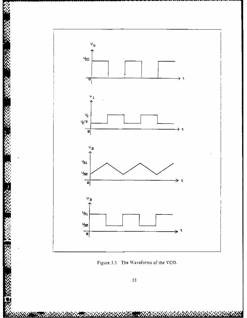
3.1 Voltage Controlled O scillator .................................. .. .. 50
3.2 Prototype Voltage Controlled Oscillator ..............................
3.3 The W aveforms of the VCO ........................................ 52
3.4 a) Rising Integrator (b) Thevenin Equivalent circuit (c) FallingIntegrator ....................................................... 55
3.5 Falling Integrator W aveform of Figure 3.4(c) .......................... 56
3.6 (a)XOR and LP Circuit for a Square Signal Phase Detection (b)Inputand Output Waveforms of XO K Operation ............................ 58
3.7 Characteristic of the EXCLUSIVE-OR Logic Circuit of Figure 3.6(a) ...... 60
3.8 (a) One-pole Low-Pass Filter (b) One-pole Low-Pass Filter WithPhase-lead Correction Network ..................................... 61
3.9 A m plifier for the PLL ............................................. 62
3.10 Block Diagram of a Phase-Locked Loop .............................. 63
3.11 Linear M odel ofthe PLL .......................................... 64
3.12 Prototype Voltage Controlled Oscillator VCO ......................... 70
3.13 VCO Frequency-Voltage Relationship ................................ 70
3.14 (a) The Output of the Integrator (0.5 volt, div.) (b) The Output of theVCO (5 volt div, 5 psec, div) ........................................ 71
3.15 The Prototype Phase-Locked Loop .................................. 72
3.16 (a) Magnitude Response of the Loop Filter ........................... 74
3.16 (b) Phase Response of the Loop Filter ............................... 74
3.17 Frequency Response of the Loop Filter from a Spectrum Analyzer ........ 75
3.18 The Bode Plot of the Transfer Function .............................. 77
3.19 The Bode Plot of the Error Function ................................. 77
3.20 The Phase Step Response of the Transfer Function ..................... 78
8
i7
3.21 The Phase Step Response of the Error Function....................
3.22 The Frequency Step Response of the Error Function .................... 79
3.23 (a) The Information Si2nal f = 300 KHz. (b) The Output of the PLL((.; Volt div., lnisec div) .......................................... 9
4.1 (a) C lock C ircuitry ..... .......................................... 80
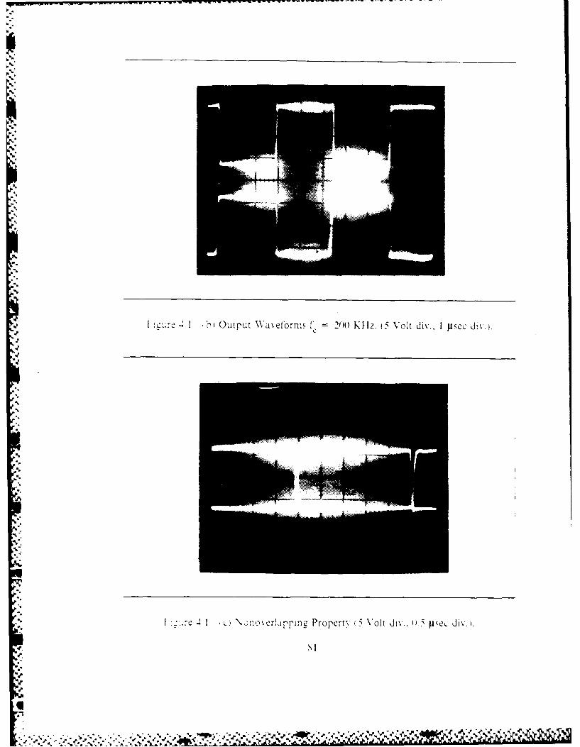
4.1 (b) Output Waveforms f = 200 KHz. (5 Volt div.. 1 psec div.) ........... SI
4.1 (c) Nonoverlapping Property (5 Volt div., 0.5 lisec div.) ................. 81
4.2 The Prototype Switched Capacitor VCO .............................. S3
4.3 (a) The Output of the Integrator (2 Volt div.1 (b) The Output oftheVCO. f = 2SS KHz.. fco =72 KHz. (5 Volt div., 5 psec div.) ............. 84
4.4 Va) The Output of the lnteurator (2 Volt div.) b) The Output oftheVCO, f = 2SS KHz., f. = 1.5 KHz. (5 Volt div., 5 Jisec div.) ............ 84
4.5 SC VCO Frequency-Voltage Relationship ............................. 854.6 SC Realization of the Loop Filter ................................... 85
4.7 (a) The Magnitude Response of Equation 4.3 .......................... 87
4.7 (b) The Phase Response of Equation 4.3 .............................. 87
4.8 The Clock Effect on the Loop Filter ................................. 88
4.9 The SC Version of the PLL ........................................ 89
4.10 (a) The Input to the PLL (b) The Output of the SC VCO (5V olt div., 20 psec div.) ............................................ 90
-4.11 (a) A Practical Realization of Figure 3.9 (b) Equivalent Circuit of(a)when (D is closed (c) when V, iN closed ........................ 91
4.12 Use of the Sample-and-hold to Obtain an Inverting Amplifier with aF ull D elay ...................................................... 93
4.13 (a) Output of the Inverting Amplifier with a Half Delay (b) Output ofthe Sample-and-hold witha Fun Delay (f = 250 KHz.,2 Volts div.. 2p sec div.) ............... ........................................ 94
4.14 () Binar-" Data Input to be Modulated (b) Demodulated BinaryD ata (5 Volts div., 1 m sec div.) ........................ ............ 95
4.15 Frequency Synthesizer Block Diagram ................................ 95
4.16 Block Diagram of a Tracking Filter .................................. 96
4.17 The Prototype Low-Pass Tracking Filter .............................. 97
4.18 The Input and the Output Waveforms of the Figure 4.17, f= 4 KHz.(1 V olt div., 20 psec, div.) .......................................... 99
4.19 The Input and the Output waveforms of the Figure 4.17, f =6.25K Hz. (T Volt div., 20 plsec div.) ..................................... 99
9
-. w -4

ACKNOWLEDGENIENTS
I dedicate this thesis to niv father-in-law.
I also would like to express my gratitude to Professor Sherif Michael for all his
teaching and understanding, and to my wife for all her understanding and help.
10

I. INTRODUCTION
A. THE NEED FOR SWITCHED CAPACITOR REALIZATIONThe periodic sampling of analog signal has been used for many years to
implement basic analog signal processing functions. These functions include amplifiers.sununers, delays, sample-and-hold, integration, and differentiation. One of the primaryadvantages of these circuits is that they provide an economic and accurate
implementation of analog circuit functions with existing integrated circuit technology.
Continuous analog circuits are composed of' resistors, capacitors, and activedevices. However, the performance of these circuits depends upon the accuracy of theresistors and capacitors. Especially in filters, this becomes a serious problem becausethe RC product must be accurately defined for a desired performance. To obtain asufficient absolute value accuracy most of the circuits designed using these elementsneed external trimming. Another serious problem is the changes in the values of' thepassive components as temperature chang',,. Resistor and capacitor values may notchange by the same amount and the same direction, which may pose a serious problem
in some critical situations. Besides these undesirable properties. large values of timeconstants require large values of resistance which also requires large areas in the
integrated circuit.
Analog sampled data techniques provide a unique solution to the aboveproblems. It will be shown that the resistor can be replaced by switches and capacitors.Ftters using switched-capacitor (SC) techniques overcome a major obstacle to filter-on-a-chip flabrication, by simulating resistors with high-speed switched capacitors. Suchan approach thus eliminates the necessity for precise integrated resistor values thatrequire costly trimming procedures and permits fabrication of precise monolithicanalog capacitor filters. This results in the important fact that the circuit performance
and the accuracy is determined by capacitor ratios. Ratios of elements are alwayseasier to control. MOS IC technology can implement capacitor ratios to within about0.3'o of specified values. [Ref. 1]. Since the only concern is the ratios rather thanindividual values of capacitors, it can be possible to use very small capacitance valuesin the integrated circuit, resulting in smaller chip areas.
I I
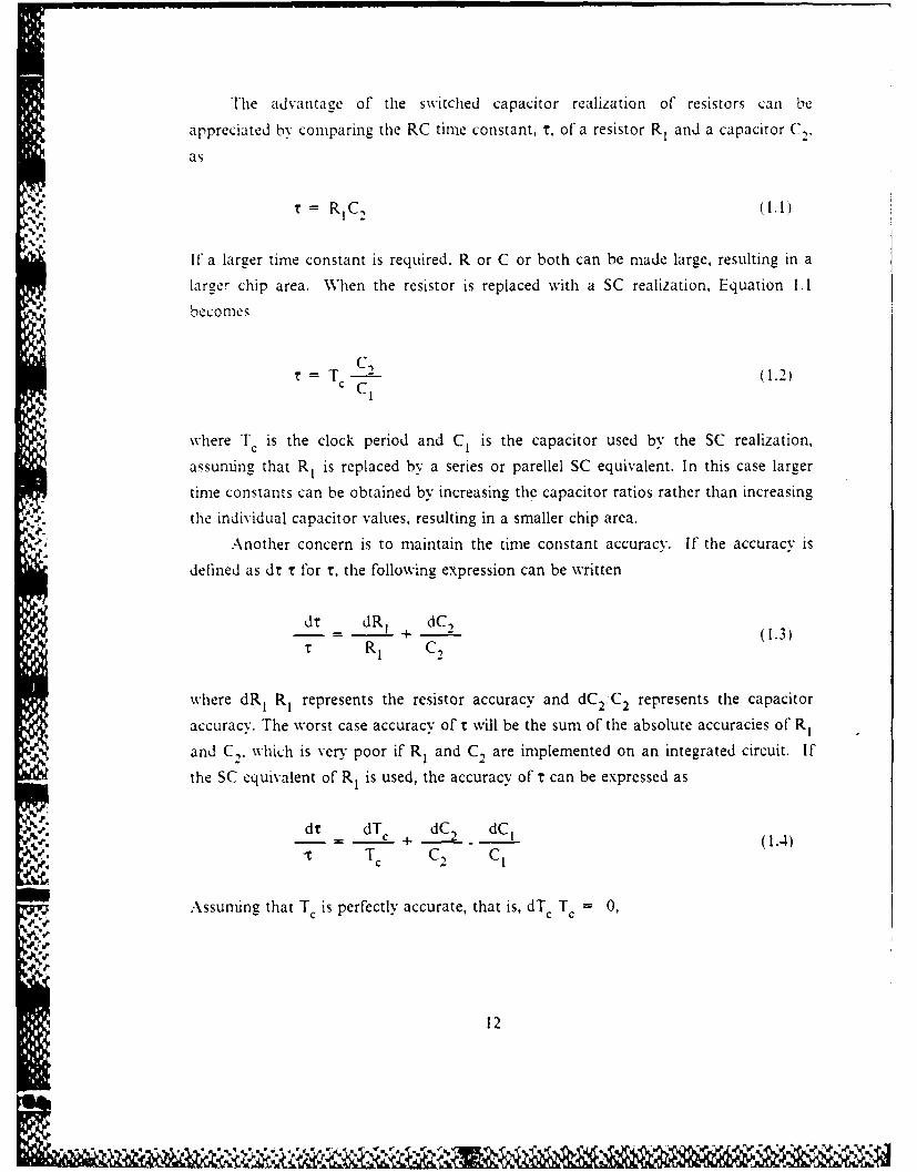
The advantage of the switched capacitor realization of resistors can be
appreciated by comparing the RC time constant, r. of a resistor R 1 and a capacitor C,.
as
.= R IC2 (1.1)
If' a larger time constant is required. R or C or both can be made large, resulting in a
larger chip area. When the resistor is replaced with a SC realization. Equation 1.1
becomes
C. (1.2)C1
where Tc is the clock period and C1 is the capacitor used by the SC realization,
assuming that R is replaced by a series or parellel SC equivalent. In this case larger
time constants can be obtained by increasing the capacitor ratios rather than increasing
the individual capacitor values, resulting in a smaller chip area.
Another concern is to maintain the time constant accuracy. If the accuracy is
defined as dr T for T, the following expression can be writtendr dR 1 , dC-)T R1 C,
where dR 1 R1 represents the resistor accuracy and dC 2 C2 represents the capacitor
accuracy. The worst case accuracy of t will be the sum of the absolute accuracies of R,
and C,, which is very poor if R, and C2 are implemented on an integrated circuit. If
the SC equivalent of R 1 is used, the accuracy of t can be expressed as
dT dT dC, dC1- = - +
(1. .)
,- c C 2 C 1
Assunung that T c is perfectly accurate, that is, dT Tc 0,
., ,
12
I WIT "-. .. .. I

d dC, dC( ( 1.5)C, C1
Because the two capacitors C1 and C., are built close together, using the same
technology, the acuracv of Equation 1.3 is much improved over that given in Equation
1.5. Furthermore. because the capacitors are similar in many respects, such properties
as linearity and temperature coefficients are well behaved. When the temperature
changes, their values change by the same amount toward the same direction, leaving
the ratio almost constant. This is indeed a very satisfving result when T must be
carefully controlled.
B. SWITCHED CAPACITOR EQUIVALENT RESISTORS
A Switched-capacitor consists basically of a capacitor whose charge is transferred
from one node to another by a switch, thus simulating a resistor.
The switched capacitor resistor of Figure 1.1 (a) is called the parallel switched
capacitor resistor realization. It simulates the circuit of Figure 1.1(b). The switch
, symbol will always be drawn open. It will be assumed that the switches are controlled
by the application of a two-phase clock. The period of time is divided into two equal
segments as illustrated in Figure 1.1 (c). The segments will be called phase periods. It
will be assumed that the phase periods are seperated by a finite period of time in which
all the switches are open. This situation is called nonoverlapping clocks, which is aver- important property for switched capacitor networks. The open-closed positions of
the switches will be determined by the phases of the clock, the switch is closed when
the waveform is high and open when the waveform is low.
It can be consider that the analog sampled data realizations correspond to one
topology during the 02 (or (D) clock phase and to a second topology during the 0,
(or (D,) clock. A useful complementary notation for the clock phases is denoted by
even and odd, which can be associated to (2 and 01 by definition. In fact, practically,
to ensure that the even and odd switches are never turned on simultaneously, the
clocks are made nonoverlapping (i.e., the duty cycle is slightly less than 500o). It is
noted that turning both the (D and (o switches off simultaneously does not affect the
behavior of the circuit.
13

v, cv t va
(U) (b)
aI I I I t
T/2 4 3T/2 IT
(c)
Figure 1.1 Parallel Switched Capacitor Realization.(a) Switched caa'cItor realization of a continuous resistor. (b) Continuous resistor.
(c) lock waveforms for the switched capacitor realization.
Both input and output of the SC network are sampled data signals which change
in value only at the switching instants kT. Thus, the voltage sources and internal
circuit voltages are assumed to be sampled at times kT and held over a one-half clock
period interval, T. To illustrate graphically, the sampled-data voltage waveform in
Figure 1.2 (a) can be partitioned into its even and odd components as shown,
respectively, in Figure 1.2 (b) and (c).
Mathematically it can be expressed as
v(t) = vo(t) + ve(t) (1.6)
or in the z-domain
V(z) = Vo(z) + Ve(z) (1.7)
14

Lict)
0 T 2T 3T 4T ST ST
a)
Vo ct)
a T 2T 3T 4T ST ST
(b)
ie ct)
C)
Figure 1.2 (a) Sampled Data Voltage WaveformsPartitioned into (b) Even and (c) Odd Components.
15
,. ,.
where
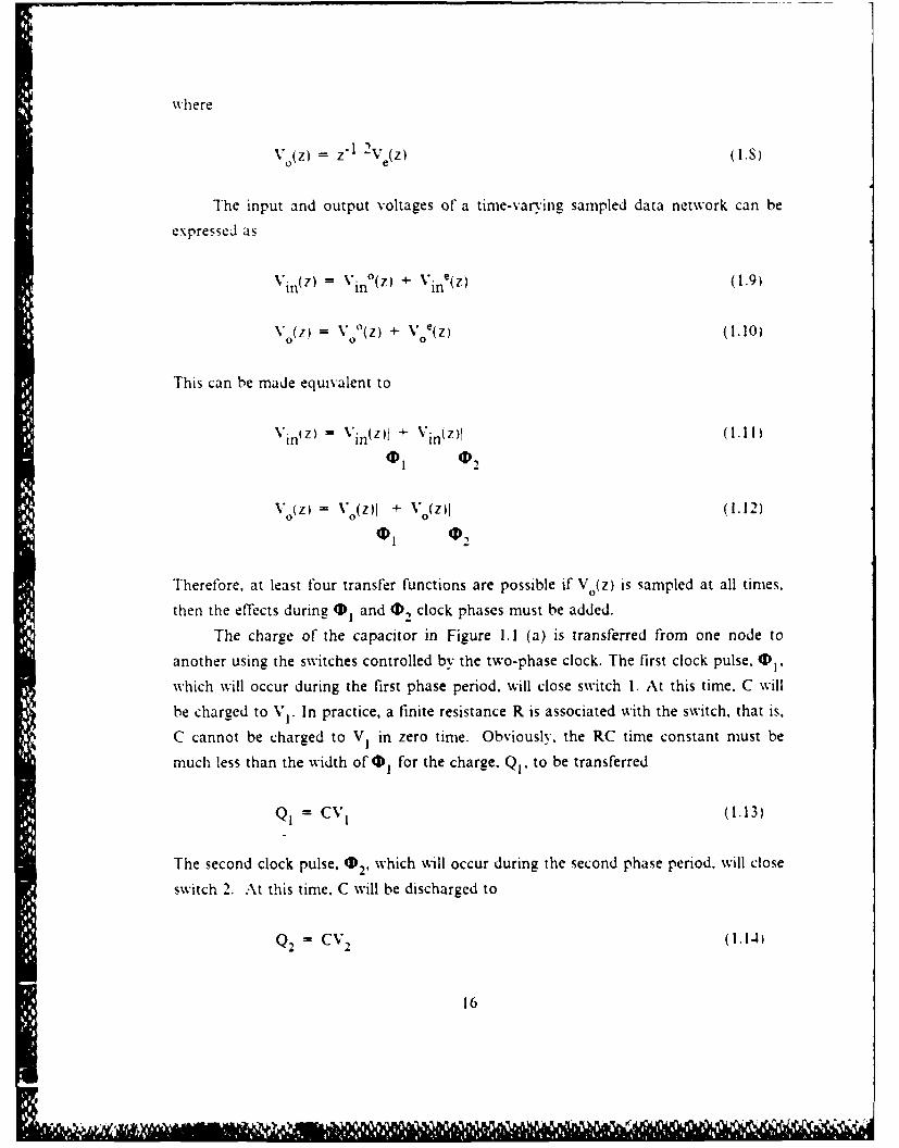
VO(Z) = Z 1 2 V(z) (l.S)
The input and output voltages of a time-var'ing sampled data network can be
expressed as
Vin(Z) = Vin(Z) + Vine(z) (1.9)
Vo(Z ) Vo (z) + Voe(Z) (1.10)
This can be made equivalent to
VinZ)-- Vin (z) + Vin(Zj (1.11)0v1 02,
Vo(zi I Vo(ZI + V0(z) (1.12)
Therefore, at least four transfer functions are possible if Vo(z) is sampled at all times.
then the effects during 01 and (, clock phases must be added.
The charge of the capacitor in Figure 1.1 (a) is transferred from one node to
another using the switches controlled by the two-phase clock. The first clock pulse. 01,
which will occur during the first phase period, will close switch 1. At this time. C will
be charged to V1. In practice, a finite resistance R is associated with the switch, that is,
C cannot be charged to V1 in zero time. Obviously. the RC time constant must be
much less than the width of 4b for the charge. Q1. to be transferred
Q1 - CV1 (1.13)
The second clock pulse, 02. which will occur during the second phase period, will close
switch 2. At this time. C will be discharged to
Q2 = CV 2 (1.1
16

An amount of charge equal to AQ = Q, - Q, is transfered from one terminal to
another. This charge transfer represents an equivalent current of
AQ VI,1 = - " (1.15)T I
-TC
and the form of this equation indicates that the switched capacitor can be modeled as a
resistor of value
1Req- fC (1.16)
C
where f = I T is the switching frequency in Hertz. The switched capacitor resistor ofC
Figure 1.1 (a) is called the parallel switched capacitor resistor realization. [Ref. 2].
A second switched capacitor realization of the continuous resistor is given in
Figure 1.3. This configuration is called the series switched capacitor resistor realization
of the continuous resistor.
In the series case. V1 is connected to V, through C for a portion of the clock
period, the second phase period. The first clock phase makes the capacitor short
circuit, therefore. Figyure 1.3 is valid only at 0,- '-- QI = 0
Q2 C(V2"- VI)
AQ= Q " Q2
SQ = C(V 1 -V2 )
Using the above equations, we find Equation 1.15 and Equation 1.16 again for the
series switched-capacitor case.
A third realization is a combination of the parallel and series configuration and is
shown in Figure 1.4. This configuration is called the series-parallel realization of a
resistor. The circuit can be analyzed by using similar technique as for the previous two
realizations. At (D or t = T 2. the charge which flowed across the left dotted line in the
direction of i is shown in Figure 1.5 (a). This charge is
QI(T 2) = CV 1 (1.17)
17

02 1
+ +
| m m |! I I!! [
Figure 1.3 Series Sitched Capacitor Realization of a Continuous Resistance.
+ 1+
Figure 1.4 Series-Parallel Switched Capacitor Realization of a Continuous Resistance.
18

Cl
+ +
, c2 C V2
((b)
Fi ure 1.5 Series-Parallel Switched Capacitor Realization.fa V.first phase period (b) P2' second phase period.
At 0)2 or t -T, the charge which flowed across the right dotted line in the direction of
S2is
Q2(T) - CI(V 2.Vl)4.C 2 V~2 (1.18)
An amount of charge equal to AQ -Q, - Q2transfered from one terminal to another.
This charge transfer also represents an equivalent current, 1;
AQ - C2V1-C1V2 +C IV .C 2 V2- (VI- V 2 )CI+ C2)
I A Q (V _2 (1.19)T IT
C I+C 2
19

and the form of this equation indicates that this type of realization can also be
modeled as a resistor of value
TIReq = T- = (1.20)Req C+C 2 (C I + C2)f ¢
if C1 W C, - C, then;
l- (1.21)I
Req = 2Ofc 1-1
when Equation 1.16 and Equation 1.21 are compared, it can be seen that the series-
parallel realization may result half the equivalent resistance value for the same clock
frequency.
VV+1 T ._I __ I .- I - I.
I I
Figure 1.6 Bilinear Switched Capacitor Realization of a Continuous Resistance.
A fourth switched capacitor resistor realization is shown in Figure 1.6 This
configuration is called the bilinear switched capacitance realization of a resistor. In the
20

bilinear SC resistor realization, a complete clock period is really T'2 rather than T,
because the input signal waveform is sampled twice in a single clock period.
It can be shown that this realization results in an equivalent resistor given below.
T I.Req 4C = 4C (1.22)
Although the bilinear realization has basically the same performance as the series-
parallel realization, there are some practical differences that are important. When each
of the above realizations is replaced by the resistors in an analog network, resulting in
a switched capacitor network, each will be found to possess different properties. This
will be shown in the following chapter.
C. PHASE LOCKED LOOP (PLL)
A phase-locked loop is a device by means of which the phase of a frequency-
modulated oscillator output signal is forced to follow the input signal. A diagram of
this device is shown in Figure 1.7.
*/ Figurse .7.. Phas.. Lokedsi Loop.. Sytem. (PLL)..
t o
I~~o VoItaBge
ContrPoll ed
Osc 1illat;or
21* S p- * - * *
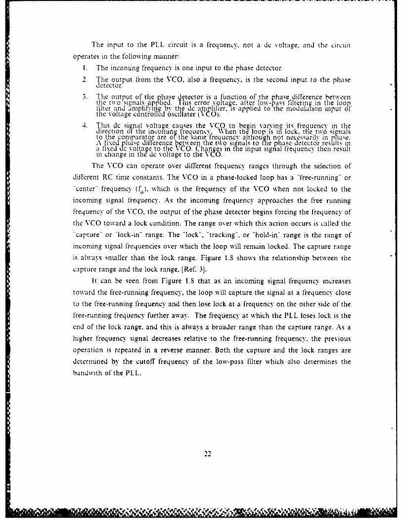
The input to the PLL circuit is a frequency, not a dc voltage, and the circuitoperates in the following manner:
1. The incoming frequency is one input to the phase detector.
2. File output from the VCO, also a frequency, is the second input to the phasedetector.
3. The output of the phase detector is a Function of the pha5e difference betweenthe two -ienals applied. This error voltage. after low-pass filtering in the loopfilter and mplif\ini by the dc amplifier, is applied to the modulation input ofthe voltage contfolld 6scillater OVCO).
4. This dc signal voltage causes the VCO to begin varn-ing its frequency in thedirection 61 the incomi'n frequency. When the loop is iii lock. the tw6 signalsto the comparator are or the same'frequencv although not necessarily in phase.A fixed phase dilrerence between the two sidnals to the phase detector results ina fixed dc voltage to the VCO. Changes in the input signal frequency then resultin change in tht' dc voltage to the VCO.
The VCO can operate over different frequency ranges through the selection of
different RC time constants. The VCO in a phase-locked loop has a '"free-running " or
center" frequency (f ). which is the frequency of the N'CO when not locked to the
incoming signal frequency. As the incoming frequency approaches the free running
frequency of the VCO, the output of the phase detector begins forcing the frequency of
the VCO toward a lock condition. The range over which this action occurs is called the
"capture" or "lock-in" range. The "lock", "tracking", or "hold-in" range is the range of
incoming signal frequencies over which the loop will remain locked. Tile capture range
is always smaller than the lock range. Figure 1.8 shows the relationship between tile
capture range and the lock range, [Ref. 31.
It can be seen from Figure 1.8 that as an incoming signal frequency increasestoward the free-running frequency, the loop will capture the signal at a frequency closeto the free-running frequency and then lose lock at a frequency on the other side of thefree-running frequency further away. The frequency at which the PLL loses lock is theend of the lock range. and this is always a broader range than the capture range. As ahigher frequency signal decreases relative to the free-running frequency, the previous
operation is repeated in a reverse manner. Both the capture and the lock ranges aredetermined by the cutoff frequency of the low-pass filter which also determines the
bandwith of the PLL.

vcoControlISignal
Locked lo
Direction o
input frequenc
rnquenfrequency
capture range
Contra l lock rangeSignal
IDirection o;inu frequency1
V~r > _____ frequency
requencyj
- j~.-Locked lop
Figure 1.8 Capture and Lock Range of the PLL.
23
~ p~ ~~% "( *' * V

II. SWITCHED CAPACITOR EQUIVALENT RC NETWORKS
In this chapter, the main goal will be developing realizations for continuous RCpassive networks. The realizations of such networks are done by the replacement of thecontinuous realizations developed in the previous section.
As an example an RC passive low-pass filter will be realized using switched
capacitor equivalent resistance technique, resulting an analog sampled data realization.
"R1
A+ 0+
-4 C 2 V 2
- -
Figure 2.1 Continuous RC Circuit.
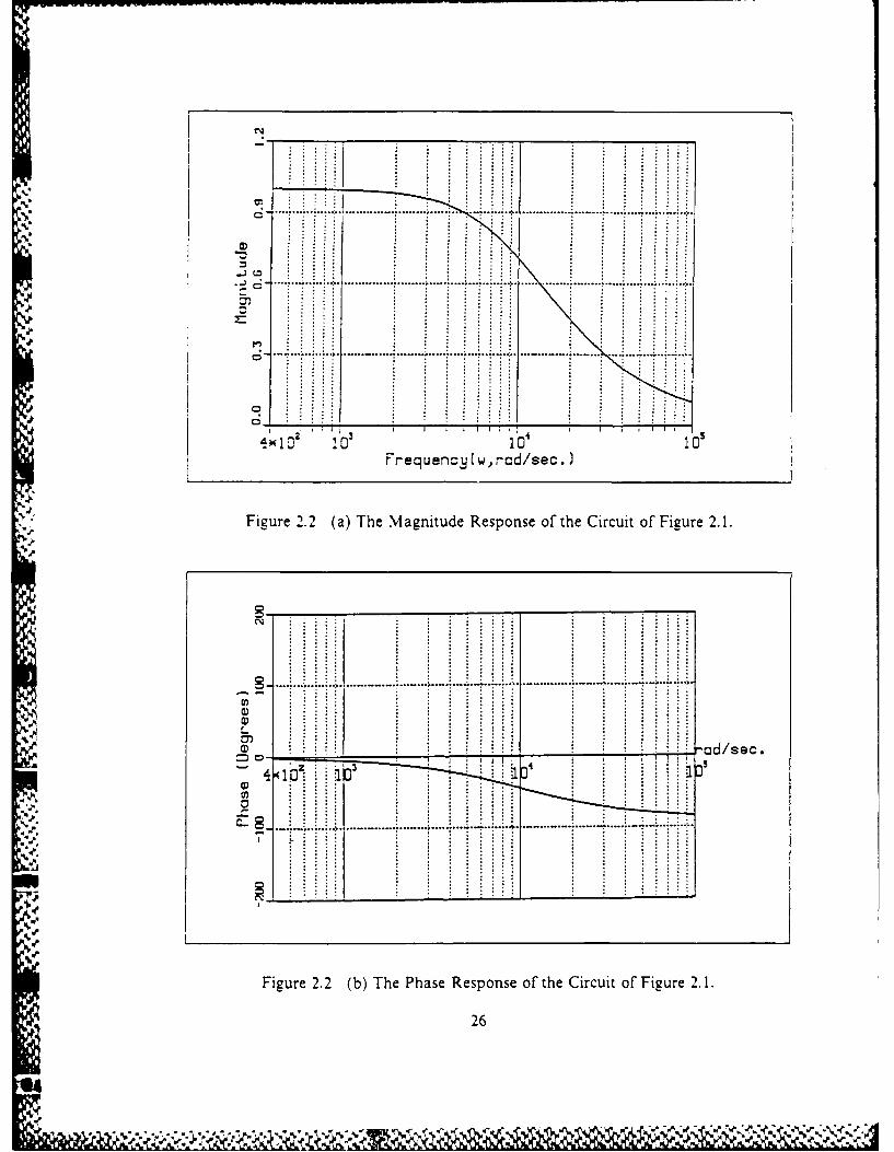
In Figure 2.1 the continuous frequency domain transfer function of this circuit is
given as
I IH(s) = = (2.1)
Sri + I s/wI + 1
where r1 = RiC 2 and w = 1/I1. The magnitude of the frequency response is given as
IH(jw)l = [I +(wRiC2)2] 1' 2 (2.2)
and the argument or phase shift is
24
' . - Zi S

.\rg lhjw) = -tan'l(wR 1C2 ) (2.S)
The frequency response of Figure 2.1 is 2iven in [igure 2.2. As an example R,1 10
KM . C, = 10 nF. and w1 = 10 x 103 rad sec were chosen to observe the frequency
response as a graphical application.
An analog sampled data realization of Figure 2.1 can be obtain by replacing the
resistor with one of' the switched capacitor equivalent resistances developed in the
previous section. But it will be shown that such an equivalence may not hold true when
the realizations are used to replace resistors of an RC network.
A. PARALLEL REALIZATION
Figure 2.3(a) shows a switched capacitor RC realization using the parallel SC
resistor equivalent of Figure 2.1. To analyze this circuit, the clock sequence has to be
identified. Figure 2.3(b) shows the necessary two phase clock sequence. (1) and (2
specify the phase periods during which switches designated as ( I and 4D, close and will
be denoted as the odd and even phase clocks. The odd phase period can be arbitrarily
defined as (D,, of the two phase clock. Therefore. the period of time where
(n+ t) - t T < (n+t+ 1 2) odd ((Dl) phase period
(n+ t- 1 2) -< t T < (n+1+ 1) even (D,) phase period.
1lwhere t = ....-2.-I .0.1.... corresponds to the tth clock period. The phase periods have
been defined to include the left end point only. This convention assures that the
nonoverlapping property is preserved. In the analysis of Figure 2.3(a). it will be
assumed that v,(t) is constant during each phase period. Let us consider first the odd
phase period where
(n-i) < t T < (n-l 2)
During the operation of the switch D1, it will be assumed that the switch (1 closes
inunediatelv after t = (n-l)T and that C1 is instantaneously charged to v 0[(n-1)TI. In
practice. the time required for v, to charge this voltage value should be small compared
to T 2. The same situation can also be applied to the (D, switch during its phase.. period. The only concern is that the switches must be closed long enough to transfer
the charge. Otherwise the clock circuits would face very severe timing requirements.
During the odd phase perid (l' Figure 2.3(a) can be redrawn as shown in Figure
2.4(a). From this figure it is seen that
Vcl(t) = v1 °[n-l)T] = v1 (n-l) (2.4)
25
... .. .. ... .. .. ... .. .... ........ . .....
N ...
..L.. ... ...........
. . .. ... ........ .... .. .. . ..
1 0 - '10101
Frqe0 wrd/e.
.. .. ...... ..........
0~L
Figure 2.2 (b) The Phase Response of the Circuit of Figure 2. 1.
26
4..01

tJt + C, C 2 V~t\A 2
(a)
I I I t/Tn n-n32 n-1 n-1/2 n n+1/2 n+1
(b)
Figure 2.3 Switched Capacitor Realization of Figure 2.1.(a) Parallel Configuration. (b) Clock Phasing.
Vc2(t) = v2°[(n-1)T] = v2°(n-l) (2.5)
After this point the clock period T in Equation 2.4 and Equation 2.5 will be dropped
because it adds no useful information and simplifies the notation.
In the next even phase period (n-I/2)< t/T< n, the (D switch is open, and the
(D, switch closes. Figure 2.4(b) represents Figure 2.3(a) during this phase period. Atthe same time C1 and C2 are paralleled, resulting in a new value of v2. Figure 2.4(b) is
converted to Figure 2.4(c) with uncharged capacitors and the voltage sourcesrepresenting the initial voltages on the capacitors. Using superposition techniques, it
can be solved -for the voltage v2 to get
j~~o C2=2t 1 vOnI + 2 2(-(2.6)2 C + C2 C1 +C 2
if v2(t) is evalutated at t= (n-l '2),
27

Ct 2 + vt)UA=VE nI)T3 : _- t(n-I)T'3
Ca)
0+
V E(n-l)TII I
U + 1+V- n-1/*2-T V VE -I)T
cb)
C' C 2 +
• )T °"2Ui~~n- n-I)T To
T 14n-- n -ITT
Fiure 2.4 Equivalent Circuit of Figure 2.3.(a) Equivalent Odd circuit when T switch is closed. (b) Equialent even circuitwhen r switch is cloied. (c) Alternative florm of(b).
28

vOe(n-1 2) = I vOtn-l) + Cn vnI) (2.- C 1
At the next phase period.
v'(n) = .,e(n-I 2) (2.S)
using Equation 2.S and the relationships of Table 1 in Appendix A. Equation 2.7 can
be written as
CIZ 'I O( ) C2zI
C 21V,°(z) - V1°(Z) + - V2°(z) (2.9)- C + C2 C + C2
Solving for V ,(z) V°(z) results in the transfer Function 11' 0 (z) for odd-odd case.
[ 0 (z = V °)0 (z ) I z 1
V O I + l-a( I + 1z 1 (2.10
H(z(2.11)
where a C2 C 1. From Equation 2.8
V20(z) = z"1 2 V2e(Z) (2.12)
\re(z) _ I z- 2
HO°(z) = V" 0(z) l 1(2 (2.13)I Vl (Z.) l+a 1-a1 1(l 'z "
thus
H00 (z) =z' ~H o(z) (.4
since Vl°(n) = vIe(n). the other two possible transfer functions are
29
(z) -r- = \- =215)v I C (1) Vi10',
et~ fl . .. =(lez2.16)
The method used to determine the transfer function of the analog sampled datarealization of the circuit of Figure 2.1 is called conventional network analysis method.[Ref 21. Ihere is another approach called charge conservation. [Ref. 41. which i-basicaly an application of KirchotYs current law, where charge is used instead ofcurrent. The method characterizes the charge conservetion condition at a particularnode for all time instants of one period, T. The two nodal charge equations can be
written for one node. for the odd clock phase
qL°(t' = q1eCt) 4- qc"(t). t >t (2.17)
and for the even clock phase
qL e(t ' ) = qn°(t) + qco°e(t), t,>t (2.1S)
where t is a time reference. qL(t) is the charge left at one particular node atequilibrium. q,.(t) is the charge at that particular node from the previous phase periodcalled as the memory charge. and qc(t) is contribution charge injected at that particularnode. The superscripts of qc°'e(t) imply that the contribution charge can be from the
even or odd clock phases or both.
Let us analyze the circuit in Figure 2.3(a) using the charge conservation method.The components of Equation 2.18 can be identified as
qe(n-I 2) = (C I+C,)2e(n-I 2)
qa 1O(n-1) = Cv20(n-l
qco(n-l) = Clvl°(n-l)and for the next odd phase period
qL (n) = C,-,(n)qme(n-I 2)= C,%,e(n-l 2)
and since the contribution from the odd phase period is zero, that is.
qCO.e(t = 0
3')
V..........
usine thle aboc equations and taking the /-transform. the transler lunctmn ':1
iq uritoi 2. I() and Equation 2.13 can be obtained. If Equation 2.IS is written in tcrmis
of its .omponents
i(ClC,)vetn-I 2) = Cv 2 n-)4- ClVl(n-l
and the Elquation 2.1- in term of its components
0I ) V e( -I. C N') = n-7I + vI
= :v,e~n-I 2),,( = v e7_1 2
(( I.tC21 . /)= ('2KIv2"I)+ Ci 'lV1 5Nz)
_____- _ 7? (2.1I,)1z) (C + C,)-C,z I
7I] . V,'= - = -
I lence. Equation 2.11 was obtained again.
The switched capacitor RC realization of Figure 2.1 has demonstrated a general
property of sampled data SC networks. This property is that the z-domain transfer
function depends upon which phase period the output is sampled. There are fourpossible sampled output waveform that can be obtained for a two phase clock scheme.
The next consideration is that whether or not Figure 2.34,a) is an equivalent
realization of Fligure 2. 1. To obtain the specified frequency response in Figure 2.2. how
can U be selected! One answer to this question would he to apply the forwardtranqforrnation of Table 2 in Appendix A to Equation 2.1 to get
INS) 1 1 ~z IW I Tz"I I1l1s ) ll1z)- (2.21)s=(Z-l) [ I I-wl )Iz
Comparing Equation 2.10 and Equation 2.21 shows that
1 I w
= -- I - -C I!2L2
wI 27r w
31i
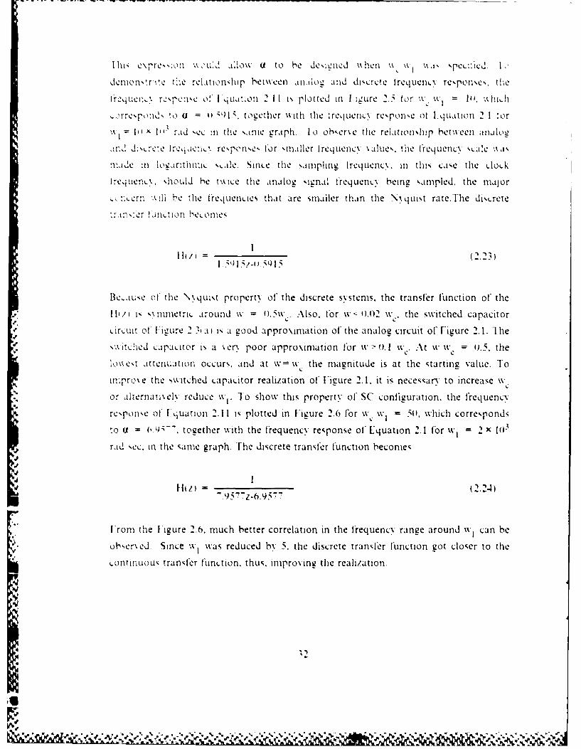
l1h1 e\p1re,0oW Ux,',d atlow u to be deMlCicd %khn x wI a, pe.licd. 1
n ontr:'te :'.e relAtI0onhlp between an.og and dicrcte lrequenm.. respole,, the
irXq C ,. r.>po :le of Ljx it.iTon 2.11 1% plotted 1n Igi'ure 2.; for A k I. : h
1o . 1'15, together with the 1rekjeC.x repone of Elquation 2 1 for
= 13 rad ,ec :n the are graph. I o obserx e the relatlonship between analog
,d d;,rcte Ireqac:i.. response, bor ,maller frequency %alues. the hrequencv tale A a,
"ade in lozarithnllc .s.,le. SICe the SaMnpling l req uency. in this, case tile clo.k
IreqUe,x . ,houtd be twice the analog signal frequemA being sampled. the major
-,: ,nLLrn x'All be the frequencies that are smaller than the NN ,qlst rateiThe discrete, :ranster [,inlt..Ofl becones
II(/1 =2. 2 31.5' I .v -'J .'-)1
Beau'e of the \. qtt property of the discrete systems, the transfer function of the
li/i iss nmietric around w = (.w Also. for w< 1).02 w_ the switched capacitor
irit' Figure 2.3 fa) is a good approximation of the analog circuit of Figure 2.1. lhe. switched capacitor is a % erN poor approximation for w> 0. 1 wC. At u' kc = 1.0. the
lo-x est attenuation occur, and at w = wL the magnitude is at the starting value. 'o
impro% e the Switched capacitor realization of Figure 2. 1. it is necessarv to increase w,
or alternatixclv reduce xv1. 1 o show this property of SC configuration. the frequency
respone of Lquation 2.11 is plotted in Figure 2.6 for w w 5il Which corresponds
to u = , together with the frequency response of Equation 2.1 for wI = 2 x 10³
rad ec. in the same graph. The discrete transfer function becomes
4Ifill4) = (2-2-1
"-95Z-6.9;77
From the Figure 2.6. much better correlation in the frequency range around wI can be
obserxed. Since 'A' was reduced by 5. the discrete transfer function got closer to the
continuous transfer fun-ction, thus. improving the reali/ation.
12As'
r,-A

CD
............ ... ... ..... ..... .......
.........
Figure 2.5 (a) 'Magnitude Response of Equation 2.23.
4 IQ: _ __ _
Figure 2.5 (b) Phase Response of Equation 2.23.
2 33
... .. . . .. ... ... ......
Figure 26 1a Pastue Response of Equation 2.4.
- Aa
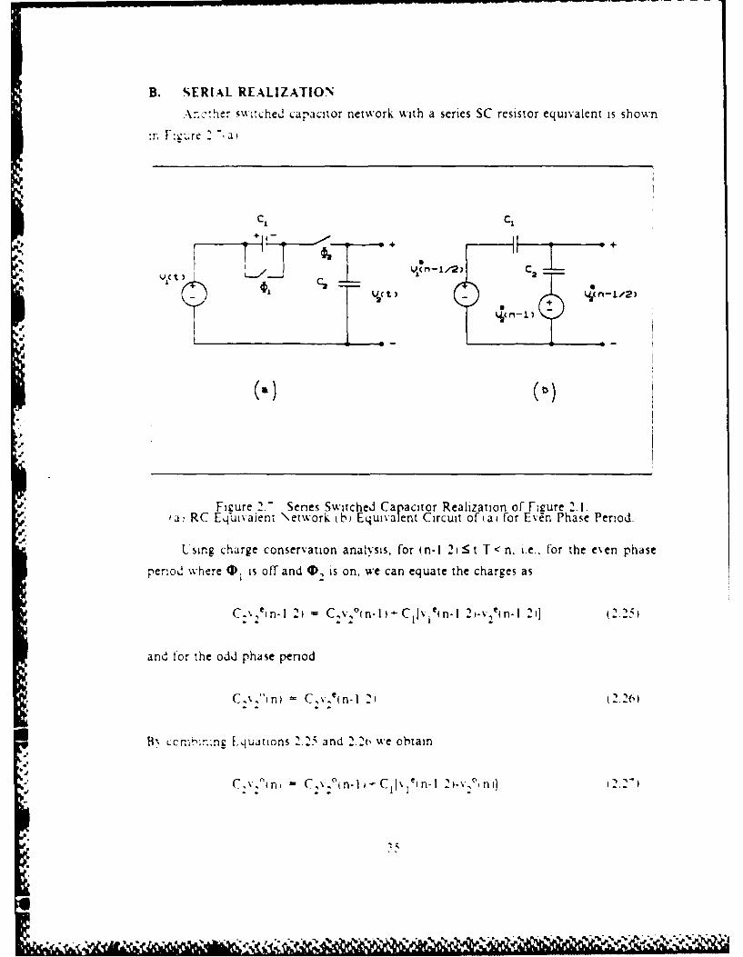
B. SERIAL REALIZATION
.-\nether s%%-itched capacitor network with a series SC resistor equivalent is shown:r. V:c' re . " a
C1 C,
T - + +
L/t 2) C
-I2 t
Figure 2." Series Switched Capacitor Realization of Fizure 2.1.Sa, RC Eqbivaient \etwork (b) Equivalent Circuit of(ai for Even Phase Period.
, sing charge conservation analysis, for (n-I 2i) t T n. i.e.. for the even phase
period where 0, is off and 0, is on. we can equate the charges as
C ,en-l. 2 = C~v n-I )-'- CI[V1 '( n-I2 j- n-l 2) 2.25)
and for the odd phase periodbo
C~, = C,v/e(n-I 2i ( 2.2('i
!21
1' Lcmrngl Equations 2.25 and 2.2o we obtain
C~v, n C~v 0( -I -C 11~ -I ~-v0~ 2%

\'2' ' ) / ) - ----- - -2('z I ( " -"\ --- -- --- -- --(-
and the transfer Function
\-,"(I I -_ 2 1= _ -___) = 1 22.29)v ) I-U) I I) ' 1 -
I rom Iquations 2.26 and 2.2. it can also be written
vl \'e~z 1 ) Z!
I o obtain the frequency response of Figure 2.7(a). it is necessary to relate a to w1.
A\nPl. i: the backwvard transformation of Table 2 in Appendix A to Equation 2.1
reLft, In
I s= I I z F 1i) = I - w (2.31)
Comparing Equation 2.3) and Equation 2.31 gives
i i wU _- - : (2.32)
It can be noted that the series switch possesses a zero at the origin. This zero
1InluencC% the phase response. The frequency response of Equation 2.29 Is given in
I igure 2.S for the case of(w, = 0. Iw ) together with the an., g frequency response for
WI = 1) x 10 3 rad sec. Since a= 1.5915. the transler function in Equation 2.29 becomes
1 2tl(7) = (2.33
2.591 5'-l. 5 15
I he frcquency response of Lquation 2.29) for the case of (w = 0.02w is alogixen in lFiure 2. tovether \ith the analog frequency repone for wI = 2 x 1)3
rad eCL. U 795--. and the transfer function is
30
~ ~ .A

* .... . . ......
-~ 5C
Fr?1ire :100--
Fiue28 (a) Magnitude Response of Equation 2.33.
~1Analg
SS
Figure 2.8 (b) Phase Response of Equation 2.33.
37

-----------------------
r requenc- W/Wcl
Figure 2.9 (a) Magnitude Response of Equation 2.34.
W/No
00
Figure 2.9 (b) Phase Response of Equation 2.34.
38

ZI2lh = - 2.34
S.95"- -. 97
it can be seen again that the sampling rate has a strong influence on the results.
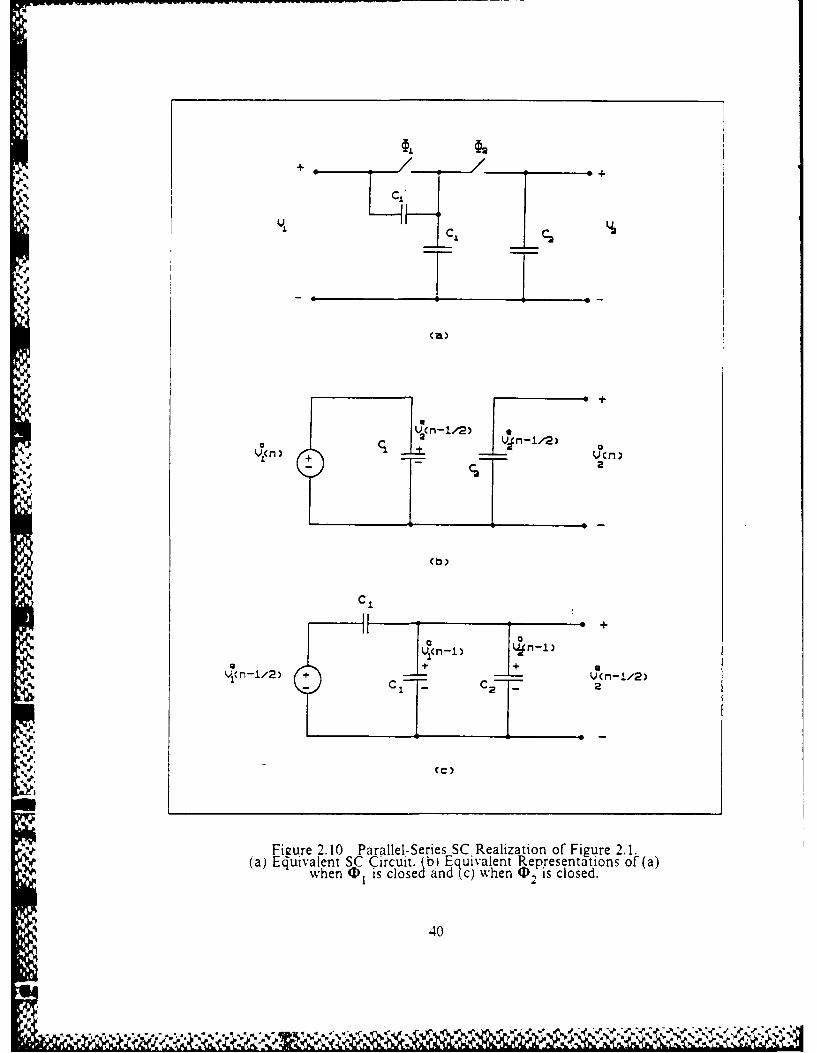
C. PARALLEL-SERIAL REALIZATION
Another SC resistor equivalent used to replace the resistor R. in Figure 2.1 is
shown in Figure 2.10i a). This implementation uses the series-parallel SC resis,.r. The
equivalent representations of Figure 2.10(a) for the odd and even phase clocks are
shown in Figure 2.10(b) and (c). The even phase period I, occurs between (n-1 2)T
and nT.
The charge conservation equation for ID, is given by
(C1 - C:)v.e(n-I 2) = C v(n-l)+ClV1 °(n-l) (2. 35
-C1 [Vle(n-I 2)-v 2e(n-I 2)]
Considering the next odd phase clock, it can be observed that
%v,e(n-I 2) = v, 0(n) (2.36)
and it is also assumed that
V1 001-I 2) = v 0 (n) (2.37)
Using the relationship of the table of Appendix A and C1 = C 2.a, = C2 C results
V,°(z) 1 1 z"1
H°(z) ) 2(l+ow ' l) l-U1 (l+at).1z. 1 (2.38)
It can be seen that there is a zero at z -1. This zero will result in a notch or zero
magnitude at half the sampling frequency. To plot the frequency response and
compare it with the analog response of Figure 2.1. it is necessary to develop a
relationship between t and wI . For this purpose, the bilinear transformation of
Table 2 in Appendix A is applied to 1l(s) given by Equation 2.1. The result will be
cquated to Equation 2.38.
39
,1
+ -+-/ /
,€ ,,
. ,,,
Cl C2
(Ca)
+
h l and-1/2) .hn c
22
cb)
C
+
Jr,-1/2) + V(n - 1/2)1Cl CZ - 2
CC)
N' Figure 2.10 Parallel-Series SC Realization of Figure 2.1.(a) Equivalent SC Circuit. b) Ejuivalent Representations of (a)
when (D is close And c) when 0is closed.
*1~ 40

4lhS) = lltz) = -+- w 42 3Sa4-s 1 -
*I l1-ZT I -z -1 -
1+
In this passive RC case. the series-parallel SC resistor equivalent corresponds
exactlv to the bilinear mapping if
i w 1 - (2.4)
The frequency response of Equation 2.3S is given in Figure 2.11 for the case of
(wI =O. .1w) together with the analog frequency response for w I = 10 x 103 rad sec.
since (t = 1.0915. the transfer function in Equation 2.3S becomes
[H(z) = - (2.41)" ' ~~2 (1 l)(ll
0.5z+ 0.5H(z) " (.422.0915z- 1.0915
The frequency response of Equation 2.38 for the case of (w, = O.02wc ) is also given
in Figure 2.12 together with the analog frequency response for w1 = 2 1 103 rad sec..
C11 = 7.4577, and the transfer function in Equation 2.38 becomes
0.5z + 0.5= (2.43i)
8.4577z-7.4577
D. BILINEAR REALIZATION
The last SC realization of Figure 2.1 to be considered is shown in Figure 2.13(a)
and uses the bilinear SC resistor simulation. Figure 2.13(b) and (c) show an equivalent
circuit for Figure 2.13(a) during the (2 and (D, phase periods, respectively
41
1 , , ..: .- . , --. ...-, -., 7. -.-.- , - . , , -, , .; . -' ; ,

.0 . . . ........................ ....
-D
4mlO-'10 10 1 0OFrequency (W/Wc)
Figure 2.11 (a) Magnitude Response of Equation 2.42.
Ana log
L
22
Figure 2.11 (b) Phase Response of Equation 2.42.
42

..'.~~ ..T ..
4X10 10,-0-Fr-equencoy I W/W:)
Figure 2.12 (a) Magnitude Response of Equation 2.43.
'Vn I .. *
0
Fiur 2.2() hs esos o qaio .3
,X,

+ CL
V~t)
22
• -, • -4_
Ca)a
(a)
ci
C IQ+
CC
C2 + _(_-_/+
l (01
U C1
Ucn-1/2) C 2
0 2
0 VCn-1/2)o n) C2I
(C)
Fi2ure 2.13 Bilinear SC Resistor Simulation of Fi2ure 2.1(aTEquivaLent SC Circuit (b) An Equivalenst Circuit for fa)
during the T, Phase Period (c) During the (VI Phase Period.
44

,'c e en phae period (D, occurs between (i- i 2)!I and ni. I s cIhrCed tothe v'"u~
vc e(n-l 2) = en-I 2)-\<(n-I 2) (2.4-4)
and C, 1, charged to
V e - 2C) - \'(n-I 2) (2.45)
.\t the beginning of the next odd phase (. n - t T < (n 4- 1 21. usinP the charge
conservation approach. the component of Equation 2.17 can be identified as
qL (n) = Cv,(n) (2.16)
Sqe(n-I 2) = C,%e(n-I 2) (2.47)
q c° 'e = Civce(n-I 2)+ClVc 0(fn) (2.4s)
where
Vcl°(n) = v,°(n)-v20(n) (2.49)
Combining Equations 2.46. 2.47. 2.48, 2.49. and using the z-transform. Equation 2.17
can be written as
(C1 +C 2)V2 (z) = z 1 2(C2 -C )V2 e(z) (2.50)
+CI[VIe(Z)Z-l 2 +V1 O(z)]
Sinlarly, the following equation can be obtained
42(Cl + C,)v 2e(z) = z' (C2 -C1 )V2
0(z) (2.51)
+Cl[VlO(z)Z-I 2 +VIe(z)l
,-5

during thc \ e~en pha e, period. B' suming .quation 2.5) and Iquatlon 2.1 the
tranqtcr function can he obtained as
v,( , ) V , ( I "+1-4Z 2(Iz I - v I OZ.+5a2)
where (a= C, C
In the bilinear SC resistor simulation, a complete clock period is really .Tc 2,
rather than T because the input signal is sampled twice in a single clock period. If a
new period is defined as
T' = T
then Lquation 2.52 can be rewritten
z'4-1 Z'I (z) = (2.53
( 1- +)z4-(-U) It l-((a-I ) (a + I ))z
Again, it is necessary to develop a relationship between at and w1 to plot the frequency
response and compare it with the analog response of Figure 2.1. If the bilinear
transformation is applied to H(s) in Equation 2.1. the transfer function in the z domain
is obtained, using Equation 2.39. By equating it to Equation 2.53 we obtain44 2 w
4 -_2_ wc (2.54)W 1 Tc n w 1
The frequency response of Equation 2.53 is given in Figure 2.14 for the case of
(w, = 0. 1 w). Since a = 6.3662 the transfier function becomes
7":3 z'+ 1
H(z) = - (2.55)7.')662z'-5.3662
The frequency response of Equation 2.53 for the case of (w, O.02w) is also given in
Fi2ure 2.15. ct= 31.31, and the transfer function becomes
z'+l-
H(z) = (2.56)32.83 1z-30.83 1
46

.. ... .. .. .._.__ _ .._ _ _.. _ __..... _ _._ _.._ __.._ __..._ _..._ _..._ _..._...._.. . .. .. ._.... .. .. . .. .
Frequencs k/Wo)
Ficure '14 (a) Magnitude Response oEqain2.55.
9 . .. .. . . .. . .... .. . . . . .. .. .
0S
z0 ~ o4 ' 0
(D
Figure 2.14 (b) Phase Response of Equation 2.55.
47

Fligure 2.15 (a) Magnitude Response of Equation 2.56.
rI Og
.. .... .. .. ..... .... . .. ........ ...
Figure 2.15 (bi Phase Response of Equation 2.56.

~: .c 'I~e o! "he S(' resi~tor ifl1jIl of ( !,.iricr I l-c- c cL~n
thle rXt ,. \ e lo. I~'-ia- . Ii r~t oirder et'ork (A I icuLre 2 1 -Ii,
tlhe liliprance of h1n11 tile allrhl-1: -1iln\rihrhei
An ( C 01-.dc cI r -1 cn cer ,% :tched-kLaprtLtor lo.-c~.e c ill lie
:i1~'c~ne2eJ hwa';n tile hilinear SC reli/ation S1n..e tile he ,t S( reaili/ation ohtalned
'II IIICt C rep.t rre h ain
* el.

I1. PHASE-LOCKED LOOP (PLL)
A. LOOP COMPONENTS
The essential elements of a phase-locked loop are the voltage controlled oscillatortVCO). the phase detector, the loop filter and the amplifier.
1. Voltage Controlled-Oscillator (VCO)
In the VCO. an oscillator whose frequency is controlled by a voltage, the
amount of change in frequency is directly proportional to the level of the input voltage.
ntltag VCO outputs
Figure 3.1 Voltage Controlled Oscillator.
As seen in Figure 3.1, the VCO consists of two main elements, one of them isan integrator, the other one is a comparator. As both inputs of the integrator are
constant voltages, its output is a ramp whose slope is determined by which terminal,(+) or (-), has the more positive input voltage. The ramp is negative going if the
voltage at the (-) terminal is more positive than the voltage at the (+) terminal andvice-versa. By continuously alternating the voltage at the (-) terminal above and below
-' € 5 0
mJ 0 1o

- " , r:':",. .. tr.,in aular ,., i enerated at the integrator oap,ti I hQ
," .. . i onant ro it :\ e or ne'iti e x oltae. detern ined b% 'Ah1lh Ct
Ye i c - .,'r- tern.Inlik ha the Lircr v oltage. I he OLaitpUt is nekati whenex er the -
ermi:.d . it.±e ~1, more proitl ¢ t han the i terminal %oltace.
Be:ore implementing a SC PLL. Lin analog PLL was implemented as
SprcEtxe:,l iie V(C) used in the PLI. is shown in the Figure 3.2 [Ref- 51. and operates
)A'li , -,,1ug1112 the output ol'the comparator ik initially 111(11.
I I he hih level output. v, causes the analog switch connected to it to be ON.
* 2. This caLes the voltaCe on the integrator - terminal v1. to be equal to V, i
we ignore the resistance of the switch. This makes the coetflcient, b. In [iCure
R2 1b =--=
R+- R2 3
a = I = (always)RI 2
3. Since a> b, the positive input causes the output of the integrator to be a
positive going ramp at output v, it is also shown in Figure 3.3.
.4. At this point the voltage, v , at the ( 4- ) terminal of comparator is given.
V DD [Rh ,- Rc R
, :1. .~~~~ R b +R -a] .i-Rb + 2 - 2
When the integrator output exceeds v3, the comparator output goes low,
turning the switch OFF.
5. b is now equal to I and a< b. This generates a negative going ramp at the
output of the integrator. At this point the voltage v3 is given
b D D (3.2)R a + Rh 2
6. When the output of the integrator goes below v . the comparator output. V"
coes HiGH and the cxle repeats. LUing positive fedback on the comparator
*.511

a. VUU
D4 (
D4
Fiur 32 roote olag C ntole Osiltr
52"
.4.o
.. .. .. ..
V 2
-U.0
4. V 3
U--30
0
>
Figure 3.3 The W',aveforms of the VCO.
53

prodace, a hy,tere'is Which iP a key behavior of the VCO operation. As
chige; betwveen two %alues. ,o does the comparator 4 terminal oltage. v1.
If it did not change as the ramp voltage changed, it would immediately cause
t!'e comparator to change aCain. This would eliminate any control of the
output signal frequency by VC.
To obtain a formula for the frequency of the VCO related to the input controlvoltae V let us consider the positive ramp case. rising integrator. In Figure 3.d~b)..
le °
V - - - I
the output voltage v, is given as
CR3 s sRC
V ~ V 3V~,,. = _ c t + ...c .4t
RC 2 2RC
V t[1+ J J
- 2 RC
In the negative ramp case. the falling integrator of Figure 3.4(c). the output
'.voltage v, is given as
I 1 V 2 1-JV dt 4" [[ 114-
RC C s sRC
-aV V V 2,* v - t + -N-C + C
2 RC 2 RC%4w
v tII - [1 I (3.4)
2 2 RC
If the graph of v, is dra%%n f'or the falling integrator case. because the slopes of
both cases are the same. in Figure 3.5. the graph can be linited by the v, voltage
%alues of the comparator which are given by Equations 3.1 and 3.2. These hysteresis
limts give the graph a triangular shape.
,,= V C VC t- 2 2 RC
54
tJ
. -. -. . . -. .. . -.- . . -.- . , .- ., ' . ,,, ,. . . ,, , ,.. -. . -. . -. . ..-. - -. . .,,*-...*-* . , -

51
I 4-
ru
U 7 +
"0
Ui00
Figure 3.4 (a) Rising Integrator (b) Thevenin Equivalent circuit(c) Falling Integrator.
55
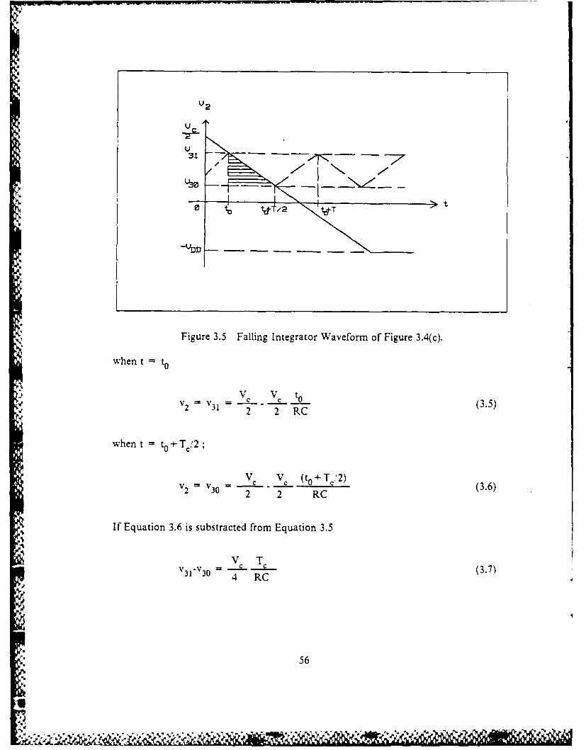
V2
V.-
31
0 t tj+/2 V~Tt
Figure 3.5 Falling Integrator Waveform of Figure 3.4(c).
when t = to
v- Vc VC to-,-V 31 2 2 RC
when t = to+T,2 ;
V2 =V30 v V (t+TC'2) (3.6)2 2 RC
If Equation 3.6 is substracted from Equation 3.5
~V Tv3 1-v 30 = VC (3.7)
4 RC
p 56
" , " " " " ".""-', """ ,","", ' " " " "" . " " "' , ,t " a"'56"
The period of the triangular wave which is also the period of the VCO output can be
obtained as
T = -C(v-V0 ) (3.8)C'Vc
The frequency can also be found as
Vf C (3.9)C 4RC(v31-v 0 ) .
It can easily be seen that there is a linear relationship between the control voltage. VC,
and the output frequency of the VCO, f'. The VCO sensitivity is defined as1C
K3 = 4RC(v31-v30 )
where the unity of K3 is Hz Volt or rad s Volt. The experimental results showed that
longer integrator outputs result in a decrease in the linearity of the VCO.
2. Phase Detector
Generally, there are two categories for phase detectors, sinusoidal signal phase
detectors and square signal phase detectors. [Ref. 61. In the square case. the signal
may be the original waveform of the signals used or may have been produced by hard
limiting followed by amplification of sinusoidal signals.
The advantage of the square signal phase detectors is that the output of the
phase detector is independent of the input voltage levels, eliminating the automatic
gain control requirement. The other important advantage is that the sensitivity K1 of
the sinusoidal phase detectors is not constant within an interval (0.) or Formed of
truncated sinusoids. However, when the signals involved are square waves, or when it
is possible to transform them into square waves, phase detectors featuring a linear
characteristic over a certain interval are fairly easy to construct.
In Figure 3.6(a) the EXCLUSIVE-OR output signal can be used as a linear
phase detector, resulting 0 when signals e'. and eR have the same sign. and I
othervise. The network implements the function
a. 5-7
'€

et)
U(t)
P5( t
r-6c t
V~t)
I L
cb)
Flizure 3.6 (a)XOR and LP Circuit for a Square Signal Phase Detection(b)Input and Output Waveforms of XOR-Operation.
58

N(t) = A Sine ( Sign [eR] 3.)
If the v(t) signal dc component v is extracted by low-pass filtering, the value
of the dc component of the signal v(t) can be calculated as a function of the phase
difference. (D = (i- o, (i representing the input signal phase, and (D representing theVCO output signal phase
T- __ - v(t) dt
T0
when 0 < (D < 7C
A to T 2 T 2+to Tv = [jdt + J -dt + I dt + - dt]
0 to T 2 T 2+t o
- A. (4to-T)T
2.:x T
v - (2to --T
- 2A itv - -(D- ) for0 < ( < it (3.12)
it 2
where (K) (to T) 2n. The corresponding characteristic is represented in Figure 3.7.The phase detector sensitivity value is
dv 2AK1 = I d I = (3.13)
The characteristic can be made independent of signal es(t) amplitude by
including a linLiter in the circuit preceding the phase detector. This implementation isalso shown in Figure 3.6a). Therefore it can finally be said that the phase detector
swnsivitv depends only on the logic voltage levels.
~59

Figure 3.7 Characteristic of the EXCLUSIVE-OR Logic Circuit of Figure 3.6(a).
3. Loop Filter
Loop filters are lowpass filters that are set between the phase detector output
and the amplifier input. The transfer function of the loop filter has a considerable
influence on the properties of the loop. The simplest low-pass filter to construct is the
RC filter of the transfer function
F(s) - (3.14)1 + Sri
where = = RC. The implementation of this transfer function is shown in Figure
3.(a). The use of such a filter produces a second-order loop. However, the
performances obtained are relatively restricted, mainly because only one parameter is
involved, the time constant t1. This prevents an independent choice of the two essential
parameters of a second-order loop, namely the natural angular frequency, w, and the
damping factor, , when the loop gain K is otherwise given.
60
4:l
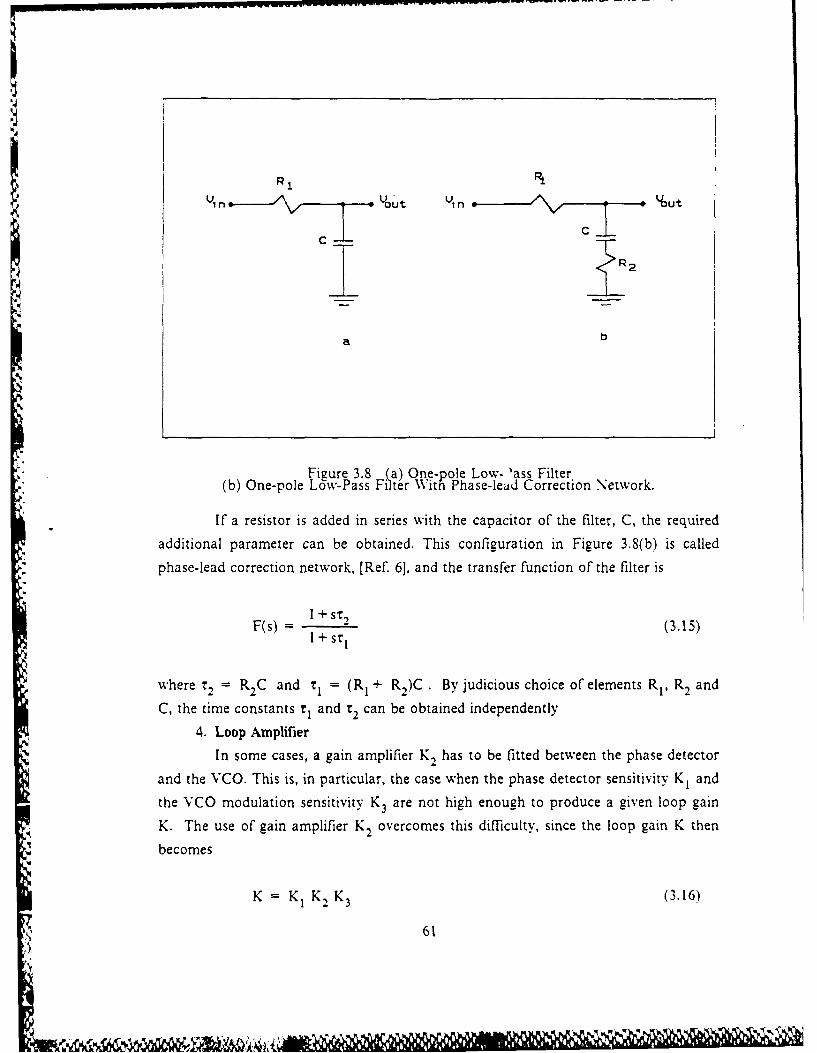
RI RVin---/ i OU't U, n: / c i " ut
CC
¢C a b
Figure 3.8 (a) One-pole Low- )ass Filter(b) One-pole Low-Pass Filter With Phase-lead Correction Network.
If a resistor is added in series with the capacitor of the filter, C, the required
additional parameter can be obtained. This configuration in Figure 3.8(b) is called
phase-lead correction network, [Ref. 6], and the transfer function of the filter is
1 + st,F(s) +- (3.15)
I + s
where r, = R2C and r, = (R1 + R,)C . By judicious choice of elements R1, R2 and
C, the time constants and can be obtained independently
4. Loop Amplifier
In some cases, a gain amplifier K 2 has to be fitted between the phase detector
and the VCO. This is, in particular, the case when the phase detector sensitivity K l and
the VCO modulation sensitivity K are not high enough to produce a given loop gain
K. The use of gain amplifier K2 overcomes this difficulty, since the loop gain K then
becomes
K = K1 K2 K3 (3.16)
61

The implementation in Figure 3.9 was used in the PLL as a hardware application. The
amplifier is an inverting type amplifier. The reason of using an inverting amplifier
comes from the stability conditions of the PLL. The gain is given as
R
RfRR
Vi nV0
Figure 3.9 Amplifier for the PLL.
B. GENERAL EQUATIONS
The phase-locked loop represented in Figure 3.10 is a device by means of which a
voltage controlled oscillator (VCO) delivers an output signal yo, in synchronism with
the input signal yi" The input signal is obtained by passing the actual input waveform
through a hard limiter. As mentioned before, this will produce a linearly behavioured
PLL.
62
1* Ii4'i or
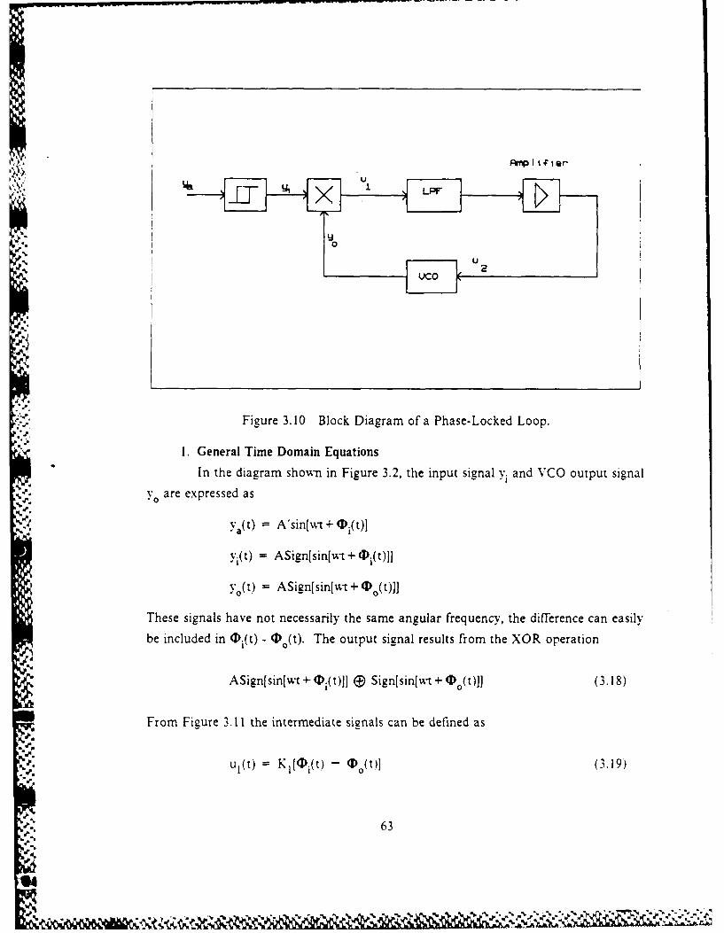
Figure 3.10 Block Diagram of a Phase-Locked Loop.
1. General Time Domain Equations
In the diagram shown in Figure 3.2, the input signal y1 and VCO output signal
yare expressed as
v (t) A'sin[wAt + it)
y1(t) =ASign[sin[,wt + Oj(t)]
y0 (t) A Sign[ sin[wt + 0(1
These signals have not necessarily the same angular frequency, the difference can easily
be included in 4Di(t) - 0 (t). The output signal results from the XOR operation
ASign~sin[wt + (Vj(t)II (® Sign[sin[w-t + (DO$t)]] (3.18)
From Figure 3.11 the intermediate sig-nals can be defined as
P.. 63

! . (ta)
Figure 3.11 Linear Model of the PLL.
where K= 2A'iT . If F(s) is the loop filter transfer function given by Equation 3.15
and ft), its impulse response, the control signal of the VCO is given as
Su 2(t) = K 2 U1 (t) * Rt) (3.20)
The symbol * represent the convolution product. Finally, since the VCO is a
frequency-modulated oscillator, K3 being its modulation sensivity in rad sec volt,
- = K3u2 (t) (3.21)
it
If Equation 3.19, Equation 3.20, and Equation 3.21 are combined, general time-domain
equation that governs the behriviour of PLL can be obtained as
d(D= K1K2K3 [ (l.(t) - )ot]*ft)(22
dt 0 (t) I ft)
* 64
04.1O
ihe product K K,K3 i repla.ed by K = KIKK I. The ccnstant K thcn
represent, the servo de[l e open-loop gain. o supply the negatite sign to the
summation. one of the constants. K K, K . should be negative. I lence. a stable PL L
can be obtained. 'he general equation is thus
d(D).,-t K [ (Di(t) - (Dot) ft) (3.23)
dt
If the Laplace transform is used. the general equation becomes
SO) = K I @i(s) - ((s) I F(s)
lH (s ) _ _ _) s ) K F (s)(Djts) s+ KF(s)
The quantity (D(s) (Di(s) = I - tI(s) is the error function of the PLL. where ()(t) is
the instantaneous phase error given by
:%@((t) = Oi~t) -- €Do(t)
The error function is given by
1 - H(s)-
.(s) s
@i(s) s+ KF(s)
The corresponding loop filter transfer function is given by Equation 3.15. If Equation
3.15 is inserted in Equation 3.24 and Equation 3.25, the transfer and error function
equations can be obtained as
Kr,s 4- KH(s) = 2 (31.2o)
+ +(1+ K,)s+ K
I - Il(s) I ( 3.2-)SS- 1 K,)s -+- K
65
1l
• . .. , , ,.,, .- ,, , . , , .. ,:..-, ,.: , ,., ,. ,., , ,-...,.. . .. , ,.,..-.. . -.-!-.....%-,,, V, ..

Linig Equa:ion 3.26 and Equation 3.?. the equations corresponding to the tinie
domain can easily be derived.
d D d$ d(I.,, 1I d (I-Kt,) +Kq (t) K, - ' (1Kt .2S ), dt -Ldt o"dt
d24) dID d2D) d(D.t -+ (14- Kt, -+ K D(t) = T1 ' + (.29dt- dt dtz dt
2. Parameters of a Second Order Loop
The denominator of the second order transfer and error functions, when
Laplace transformation is used. is generally formulated as s2 + 22" "ns + wn2 where wn is
the natural angular frequency and ; is the damping factor. It is stated, by definition.
W2 K (3.30)
2w (3.31)
The advantage of using one-pole lowv-pass filter with phase lead correction as
the ioop filter becomes more clear if Equation 3.30 and Equation 3.31 are considered:
the natural angular frequency, w~ , can easily be controlled by changing T1, and the
V,"n
damping flactor. .can be controlled by changing T2 independently. With these
notations, the quantity K(r, r)can be expressed
K-2- = 2 1 - - 24w n - n~~- (3.32)
2WT, I ( ,K
The transfer and error functions. Equations 3.26 and 3.27 respective.3 become
(D l(s) (2w w 2 Kis 2%" 2w = 2w - (3.33)
s2, + -v
661 %
Th tanfr ndero fntins qutin 3.6 an 327repetiel, ecm
IiVj.. II'.%
K
;I - Il[ ) .______.34s
C. TRANSIENT RESPONSE
In tis scction the response of the loop to different disturbances occuring at
i ;n~tant t = 1 kil -e e\ained. The diqturbances involved are
Input signal phase step 0
Irput signal angular frequency step Aw
I. Phase Step Response
\t inctant t . a 0 amplitude phase step is applied to the input signal
(Di(t) 0 7(t) (3.35)
where -,/t is the unit step fun~tion. In Laplace Transformation form
0(D=(s) - (3.36)
the phase step response of the VCO can be obtained using Equation 3.33 and Equation7.: 3.3 6.
[(2w -w 2 K)S w 2]0 Ss2 , -s) n n2 (3.37)~2 -),- 2 n rs -- 2%vnS+w12
also the phase error. (D(s) = (Di(s) - Do(s). can be derived
(D = [ - ll(s ]- (3..)S
I his leads toN
,,,.-w K O
_-V II [1ri6
.4

2. Frequenci Step Response
I:'. A:reqjuenc\ step Aw iS applied to the input signal at instant t = ()
Dt = Awt p 3.4)
,%~
',. I l.iAr'aC trar~i QrniAt~or', lorfl
I he frequency tep response of the error function using Equation 3.31 and Equation
3.-1, iven by
A %Vs= [I - 1)] ).-
,- : also lead, to
Aw XV2 A %s-.-2 \v K s)s-s2 . w s n.i
D. EXPERIMENTAL RESULTS OF THE ANALOG PLL
L sing the derived functions in the previous sections. a prototype analog phase-
ocked loop was implemented in hardware. This implementation was converted to a
,witched-capacitor realization of the PI.L. Prior to the SC implementation the
experimental results have been recorded to compare the analog and the SC versions of
the PILL.
1. Voltage Controlled Oscillator (VCO)
It is very important to build a linear VCO in some PLL applications.
o lloever, a tolerance of' 5' or 10'% on the linearity of the modulation characteristic
within the frequency variation range is more often than not acceptable, except for
.ertain applications, such as the use of a phase-locked loop as a good linear frequency
discriminator.
6 S
V.!
.4• . ',• " ," 4. % ", " .,

r tihe .ircuit in Figure 3.12 w11s built in prototype. and voltage frequeMI
relation Pi given in Figure T.. The dotted line in [ig'ure 1.13 is drawn according toLcjtuaton 3.9.
R = I Kfi
C = 30 pfS
v1l - v0 = 1.2 V 0from Figure 3.14)
The waveforms of the VCO are given in Figure 3.14. To make the triangular
wave of the integrator in Figure 3.12 short, two comparators were used. The output
voltage levels of the first comparator were .6.5,o) volts and the second comparator
output voltage levels were (-6.5.-6.5) volts. The second comparator also provided the
logic levels for the NOR operations.
2. Loop BehaviorTo construct the phase-locked loop. the configuration in Figure 3.15 was used.
[he input to the PLL can be any periodic waveform. This input is converted to a
square waveform by a zero-crossing comparator. At the same time. the logic level
adjustment for the XOR operation is done. The other input of the XOR comes from a
frequency divider. For this purpose a digital counter was used. The clock input of the
counter is fed by the VCO output. Any of the outputs of the counter can be used as
the input to the XOR. If Q, is used. the VCO frequency is divided by 2. if Q, is used.
the VCO frequency is divided by 4. if is used, the VCO frequency is divided by S.
and so on. At the same time, integer multiples of the input frequency can be obtained
when the PLL is in lock. For instance, if Q is used as an output from the counter. The
Q2 Qi" and the VCO output are integer multiples of the input frequency by 2.4. and S
respectively.
In the experiment an LF356N CMOS operational amplifier was used as the
loop amplifier. The gain K, was 5.1. This operational amplifier was also used ..
sunmmer to obtain a free running frequency for the VCO. Since it was an inverting
sunmer, the acquisition voltage was obtained from the negative power supply. The IS
K resistance can be changed to obtain a different free-running frequency of the VCO.VCO control voltage. V . can vary between 0 V and 2(VDD-I. 5 V and provides a wide
range of frequencies. The power supplies used in the prototype are (+ 6.5.-6.5 )V. so VCcan var- between 0 V and 10 V. Since this control voltage is obtained from the
amplifier and the saturation voltage of' the operation amplifier is 5V. the control
69
,'.
Sr.iga. ~.. ,''. . "".:r€.;v. &..,, ';... ,""- :.-,. ;k:,2..: ,va ~X: s"z""i9"" '*'""-' ' ;~,. : ;5""/.- ': "' '' ' ' ,.:'";

4-
UiU
UU
51
p(. L
-V

- - Theortica
.zpe flr (Vet i •
(b
g-*!-
0 2 4 6 S 10
Figure 3.13 VCO Frequency-Voltage Relationship.
i (a)
(b)
Figure 3.14 (a) The Output of the Integrator (0.5 volt div.)(tb, The Output of the VCO (5 volt iv. 5 isec div).
J71

IDI1
,mit
m m
in.
Figure 3.15 The Prototype Phase-Locked Loop.
72

voltage cannot e\ceed 5V. The other concern is the loop gain K. Since the amplifier I,
an inserting type amplifier, this provide, the required negative contant for ,tahiliit\
and suppies a positive control voltage o the VCO for proper operation.
As the loop filter, a single-pole low-pass filter with phase lead correction was
used. The time constants r, and r, In Equation 3.15 are gen as
1 R( 1 11 -- 1( b .33 x 1)-
= 3.33 msec.
which yields a pole frequency of.4S I lz. Also
,= RC
= I)() x ).3 x 1()-6
.= 33 sec.
and a zero frequency of -4.S Kliz. If these time constants are inserted into Equation
3.15. the transfer function of the loop filter is obtained as
FSW
3.15. hx loo3 .4IlI¢
The frequency response of the loop filter is riven in Figure 3.16 and the
frequency response obtained from a digital signal processor. SD-360. is given in Figure
F3.1 Referring to Figure 1.S. the capture and lock ranges were recorded as following
' fcap .-.5 Kttz.- 65 Kllz.
t ock - .5 KlIz. - 97 Kllz.
These results were obtained by connecting the VCO output directly to one of the XOR
inputs. When the PLL was in lock. the input frequency was equal to the VCO
frequency. Then. Q, output of the counter was connected to the XOR input. 1 he
corresponding capture and lock ranges were recorded as Following
1' p - 2.25 KlIz. - 32.5 K lt,.
flock 2.25 KIl . - 4.1.5 Kllz.9.E"pp..
! 9

4
U,..
q -I
...0 ............................0............. .0. . . 0
0.0 01.2 0 .4 0.6 0 .8 1 .0_ II i Fre-quenoc K~z. 1
. . .................................. ................... :................... ...................
.. .......... :................... "............................................................
Figure 3.16 (b) Phase Response of the Loop Filter.
474

I4AGNIITUDE *~~~'
-7 j
Figure 3.17 Frequency Response of the Loop Filter from a Spectrum A\nalyzer.
3Computer Simulations
To obtain a computer simulation of the PLL, the equations obtained in
section B and C were used. When the numeric values are used. the following transfer
and error functions are obtained. First, the phase detector sensitivt is given as
2 x 6.5K1 - =___ 4.138 V rad
it
K, =5. 1
K3 =2.4.46 x 103 Hz V (From Figure 3.13)
K3 =2.446 x1032n= 15.37x 10⁴ rad V
K =K 1 K2 K3
K =3.243 x 10⁶
To obtain the natural angular frequency, w , and damping factor. .Equation
3.0and Equation 3.31 are used.
75
.PdN, '~ '%. Z

4 K
11 S211S.-5 rad sec
1+ K T
The transf'er f'unction in Equation 3.33 becomes
11(s) = Ql6.S 1,15S)5.I93S4)h
The error funiction 'in Equation 1.3-4 become,;
The Bode plot of' the transfer function is given in Figure i. IS. and thle Bode
plot of' the error fuinction is given in Figure 3. 19. It can be said that the transf'er and
the error fuinction makes the phase locked loop a bandpass de~ ice. j RefI -I.
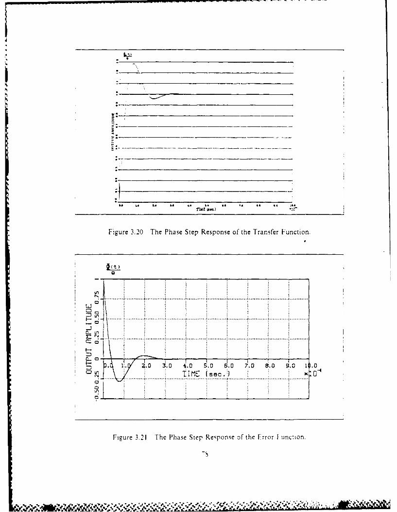
The phase step response of the transfer fuLnction Is uiven in Figure 3.2(). using1
EquaIt1In .-45. The phase step response of' the error fuLnction is given in Figure3..
u sin g Equation3.6
The f'requecy1 step response of the error F'unction is given in [igure 3,.22. using
Equation 3.42. In the last three graphs. the axis is normialited bv the amiount of the
step f-unction. 0 radians for the phase step. and the Aw rad qec for the f'requencY step
* function.
As an experiment, a frequency shift key. [SK. modulated sIgnal was applied
to the PLL. The frequencies uised were 20K11,. and SO(KI!,.. representing thle logic
levels, 0. 1 respecti\ clv. The Oscillator ou~tputs are gzi~en in I qUre 3.3 hiN fivure
aU'rees elwt FigUre 3.20i. regarding the amIount of overshoot and the settling time
of the VC() control signal.
-U0

'N
:.1
.5..
-o.
'-:"Figure SIS The Bode Plot of the Transfer Function.
- •'
',%
/*/ a
= "/ .-.- ,----
, ¥ / 'a
). /am.. /
. ".
.."5 . . . . . .. . , .... , - - - ", ,, , " - ,, " .' ,,r" " +,," " "4"' ",,,.+ - ,c" " - ;
ei Le LO Ai .@ LO GA 1.4 &.4 to 0SA
1ME Ismc) ole
Figure 3.20 The Phase Step Response of the Transfer Function.
Oct)
....... ......... .............. . ...... ......................... . .
LmUf
............................... ........... ........... ...........
-
01
01. T CD ~-~Z.~ 3.0 1.0 5.0 $.0 7.0 8.0 9.0 10.0
TIM" sec.)iA .... . .. . . .. ....... . ........ .. .. .. .. .. .. .. .. .. .. .
Fiure 3.21 The Phase Step Response of the Error Function.
aN--
-; ... ... .i... ... ...! ..... ... i ... ... .. .. ... ... i .... ... .i... ... ...i ..... ... i ... ... .. .. ... ...
" i : : " ... . .. .:.. ... .. ... ... .! .. ... . * .. .. .. -.. . .. .

.. . . . . . . . . . . . . . . . . . . . . . . ...... u l l l t P I L I I l t l l I t q l _ ia I J m ' , " , . . .. . . . . .
ssec
I,.
bI
/,I
I\ -2
F" ~ The Freq uency Stcep Respc nse o f ,he Er -r F tc-.
F,,zre 7 ( a The I romto I:ra f=3 H
I"
'p- .......................................... .................
-ai -.. , se . .. -

IV. SWITCHED-CAPACITOR REALIZATION OF PLLp A. T'WO PHASE CLOCKThe clock circuits are perhaps the most important part of an analog sampied-at ,sstemn Thysol-o e-elapping and should have a duty cycle as large as
posibi toperit charge transfer. A c-ircu t that supplies nonove-11appinz clocks fromnI a single input is shown in Figure 4.1(a), and the waveforms obtained from anoscIlloscope are shown in Figure 4.1(b) and (ci. The clock frequency can vary as the
square wave input changes.
Figure .4.1 (a) Clock Circuitry,.
To prevent the overloading, two digital CMtOS buffers were used. The other clock
circuitr components were CMOS inverters, CD4069, and CMIOS NOR gates. CD4O0l.
B. VOLTAGE CONTROLLED OSCILLATOR (VCO)The an~alog version of the VCO of FIgure 3.12 was converted to swatched
cavac:tor VCO by using the bilinear SC realization in F:igu.re 1.6. Two of the
-~ so
-1 -
, :ure -.1 Output Wavef orms f 2 0) KIIz. 5 Volt div.. c jiec div.
.
* I-rrc 4I )Noc' crLarring Propert% (5 Volt dv.. 1j.1; PweL div..
.r
ES
-.-

contMiuo\, rci1tor, were c\Juded to change the frequenc- v olta,1e .ha r,. tCritic o! the
'v V*C( ). R. and R 2 in Ficure 3.2. Since the rest of the resitors are p:,rt of the o ,,t:ie
di iders, as the Lock frequency changes, the VC(O output freq uencv rCmained contant.
The maJor problem encountered during the experiment was the distortion of the
x!aveOrms at the higher frequencies because of the fact that the clock frequency ,hould
1,e an intecer multiple of the oscillation frequency. [ Se S]. Therefore, it is important
to kep the sampling rate rather high in order to minimize the phase jitter. In order to
fInd the capacitor values for the bilinear realization. Equation 1.22 is used. The clock
frequency was 2()() Kliz.. and the calculations were made using this value. The SC
Scrsion of the VC(O is shown In I Figure 4.2 and the waveforms are show In liture 4.3
and t-icure 4.-4 for dillerent sampling rates. These waveforms agree well with the
wav'eforms in Figure 3.14. The experimental frequency-voltage relationship is given in
I i,,ure 4.5 for f' = . KIIz. The dotted line stands for the theoretical curve whose
1 equation i given in Equation 3.9. using 12 -V3 0 = V I.S Volt. obtained from Figure
C. LOOP FILTER
1. Siitched Capacitor Realization.
The SC version of the loop filter is shown in Figure 4.6. The bilinear switched
capacitor realization was used for the SC conversion. This choice was made based on
the results given in Chapter II. Since the best realization obtained from Chapter II was
bilinear SC realization, the continuous resistors were converted to their bilinear
switched capacitor equivalents. The transfer function in the s domain is given by
Equation 3.15. If the bilinear transformation is applied to Equation 3.15. the transfer
,.function in the z domain can be obtained as
-"'IT2, 2r,(1+ --- )z(1 -
T Tf-' 2 1- 1 F(z)= 2t (4.1
;Z:s=-(I _ )(1+ IT ) (l -T )
T +~ T z
Sinae the actual Cock perod is really T 2 rather than T becaise the input signal is-,, .n>..,v in a ,ingle clock period, the transfer function in z domain becomes
S2
* -- * %, %~ 44, 4% % ~/ : JJ ~ '.d ~ * .~ .i'.~ ~~ ) ~ *.~*. W
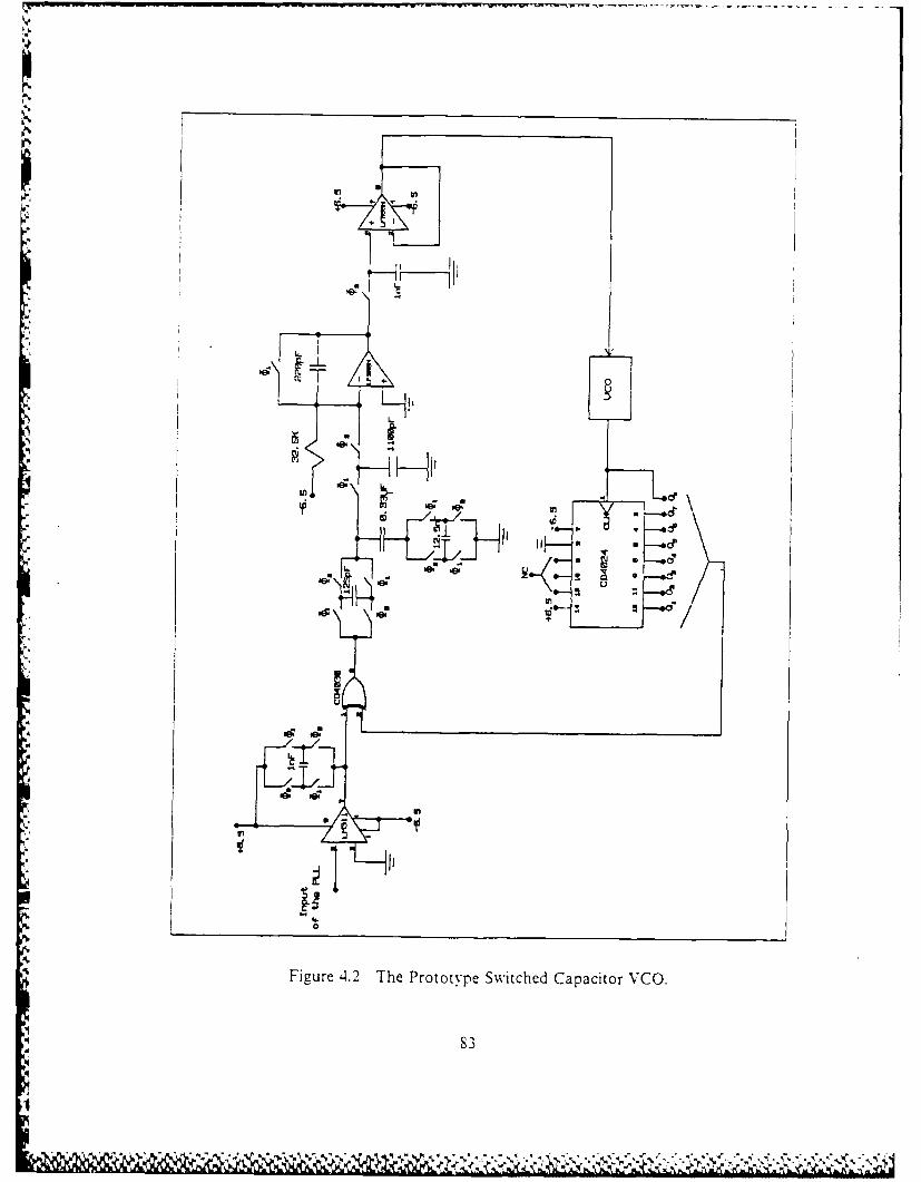
_ - - ~ -- ' ,'~ ,- ~ - --
De
soin
Figure4.2 Th Protoype Swtched apctrVO
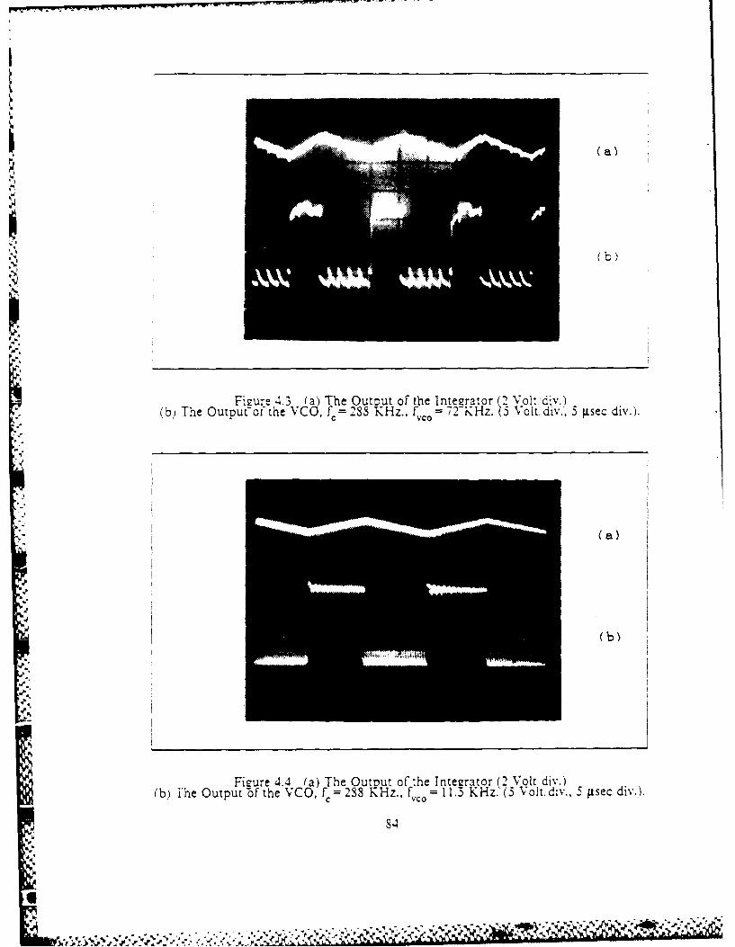
(b
Fiaure 4.3 (a) The Output of the Integrat-or (2 Volt'div.j(b) The Output~of the VCO, f = 288 KHz., fv0 72-K1-z. (5 Vo It, div." 5 g±sec. div.).
(a)
(b)
Fieure 4.4 (a) The Output of the Integrator (2 Volt div.)(b) ihe Output ~of the VCO, f~283 K1-z., f~=11.3 KHz. (5 Volt, div., 5 pisec, div.).
8.4
'Vi
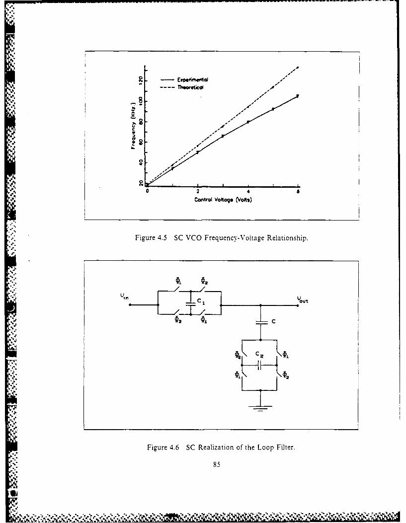
ch2-4
- Copnmntro altg(Vls
-; sq
,, c V.
CC
0 2 4 2Controd Votage C/olts)
2:3" Figure 4.5 SC VCO Frequency-Voltage Relationship.
'2L'
Figure 4.6 SC Realization of the Loop Filter.
85

- t -- It((..
4t4(1 )Z--l -
C
It' Fz is to be calculated in terms of the actual experimental values, the Followging
results can be obtained.
= 3. msec.33 Psec.
f - 200 KIIz.
and the transfer finction becomes
2..4z-25.4Fmz = ( -..132 2665z-2663(
Since the sampling rate was very high. it was not necessary to make frequency
prewarping. The frequency response of this transfer function is given in Figure 4.7.
This igure agrees well with the frequency response given in Figure 3.16.
2. Loop Behavior
The clock effect on the loop filter frequency response has a great influence onthe loop behavior of the phase locked loop. Since the continuous resistances were
replaced with their SC equivalent realizations, the constants of the filter, r, . T,. become
1 I= (C - )C (4.4)
4C 1f, 4C~f.
4 C 45
JC,f~
In the experiment C, = 125 pF, C2 = 12.5 nF, C = 0.33 pF, and f = 200 Kltz. The2 C
capacitor values were found by using Equation 1.22. The time constants were t 33
Jsec. and r, = 3.33 psec. If the clock frequency is changed, these time constants
change. If the clock frequency is increased, r and T, decreases linearly. For f. = 300
KIIz. r, = 22 psec. and the pole and zero frequencies are calculated as
86
DIX'~~-
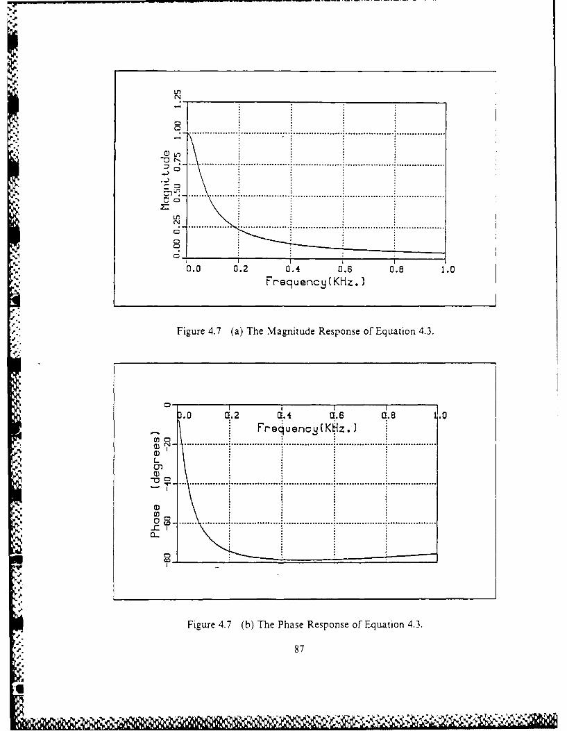
W .n
CD
F n
0.0 0.2 0 .4 0 . 0 .8 1.0
FrequencS(KHz.)
Figure 4.7 (a) The Magnitude Response of Equation 4.3.
.0 a.2 a.4 a.6 .8 .0
Fre uencS(KHz.)
L . . ... °° ....... .. ..... . . ... °° ..... ........ ............ . .... °° "°° °°°° ° ° °°°°° °°°°° °°.............
5U)CL)
co
Figure 4.7 (b) The Phase Response of Equation 4.3.
.'. 87
-S, f. " '- *" "" , . . . . . ,d ? " 0 r

- - - - -1.7 liz.S 27r 27rrI
F, = - = 7.23 KHz.- T 277t
From these results it can be seen that if the clock frequency is increased by 5010 , the
critical frequencies increase 50'%. For f = 400 KHz. ri = 1.665 wec. T, = 16.5C
pisec. and the pole and zero frequencies
f, = 96 Hz.
f= 9.6 Klz.
The clock effect is shown in Figure .4.S. The results w~ere obtained from a digital signal
processor.SDS.
HOM IlUDg
_ IT
:1:~~to Kit.. ** *f[~j{r 300 Vr.400 K i
L A
Figure 4.8 The Clock Effect on the Loop Filter.
The SC version of the phase locked loop is shown in Figure 4.9. This circuit
was obtained by substituting the continuous resistors of Figure 3.15 with their bilinear
SC realizations. The circuit of Figure 4.2 was used as the SC voltage controlled
oscillator. The picture in Figure 4.10 was taken while the PLL was in lock, F=200
KHz.. F c0 20 KHz.
88
~~%

II
:" I..[
'
1
IV
p.
'i Figure 4.9 The SC Version of the PLL.
89
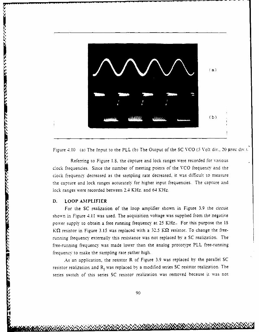
(b)
* Figure ".10 (a) The Input to the PLL (b) The Output of the SC VCO (5 Volt div., 20 psec div.).
Referring to Figure 1.8. the capture and lock ranges were recorded for various
clock frequencies. Since the number of meeting points of the VCO frequency and the
clock frequency decreased as the sampling rate decreased, it was difficult to measure
the capture and lock ranges accurately for higher input frequencies. The capture and
lock ranges were recorded between 2.4 KHz. and 64 KHz.
D. LOOP AMPLIFIER
For the SC realization of the loop amplifier shown in Figure 3.9 the circuit
shown in Figure 4.11 was used. The acquisition voltage was supplied from the negative
power supply to obtain a free running frequency at 25 KHz.. For this purpose the 1S
K2 resistor in Figure 3.15 was replaced with a 32.5 Kl resistor. To change the free-
running frequency externally this resistance was not replaced by a SC realization. The
free-running frequency was made lower than the analog prototype PLL free-running
frequency to make the sampling rate rather high.
As an application, the resistor R of Figure 3.9 was replaced by the parallel SC'r resistor realization and Rf was replaced by a modified series SC resistor realization. The
series switch of this series SC resistor realization was removed because it was not
90
1%

CC
+ +
4CC)
Figur C.11 (a+ rcia elzto fFgr
(b)EquvaentCicui () we scb
(c) whn ),i cosd
4%91

Md\~r % OUkl would aue tile Or 1111 to hlis e no0 1CCdb~h-k dorim!,olc of ~lie ri~a'c
zilte har-ecc,ncer\ atiori 1prroac.h iu Lcd to anal\ /e I qeure 4.1 ibi. thc
cconnpcI--et of I ,,LudL[1n 2.P. a re identitied I'Or the cei en clo plwtse reriod.
In- 1 I' n5tF-1
k. -it = L,,( t ) 1O .1tI t t
(n-I ) = , I)-I2
cle')n12=- IC C~ ' -I v(n.5)
%''11 *2 (C
I () - - 7 -1 2
It can be seen '-,at Fizure 4.11 acts like an1 inverting amplifier with a g~ain of' C, C, and
a delay of' T 2 seconds. Note that voltage gzain can be achieved if' C1 is larger than C,
It is also noted that at no time the op amip was without somec form of' feCedback. In thle
even phase period. C, is charged to the voltage given by [quation 4.8 and will hold
that v oltagze Indefinitely under ideal conditions. Therefore, as longz as v, '(n- I ) does not
cause v e.)(n-1 2) to saturate the op amp. the circuit performs as expected.
It is observed that the z-domain transf'er Function is multiplied by a hadIdelaN.-I -1-1Ths z1 2 ca e hned to a full delav.z . bythe use o - a samiple-and-hold
cici.The circuit is given in Figure 41.12.I lee i issee tht drin th ~ has Ovn) is stored in the holding capacitor
C er itiDnta uring the nexthas v In
Ch'Durng he extph~ase period, whn( closes. vn is available at %0h* Theref'ore
V v110 (n- 2) = vo e(n) (.0
*~~ ~~~ V = \we( 1 2 -(C 1 C2 )7Z\ 07 (.
92
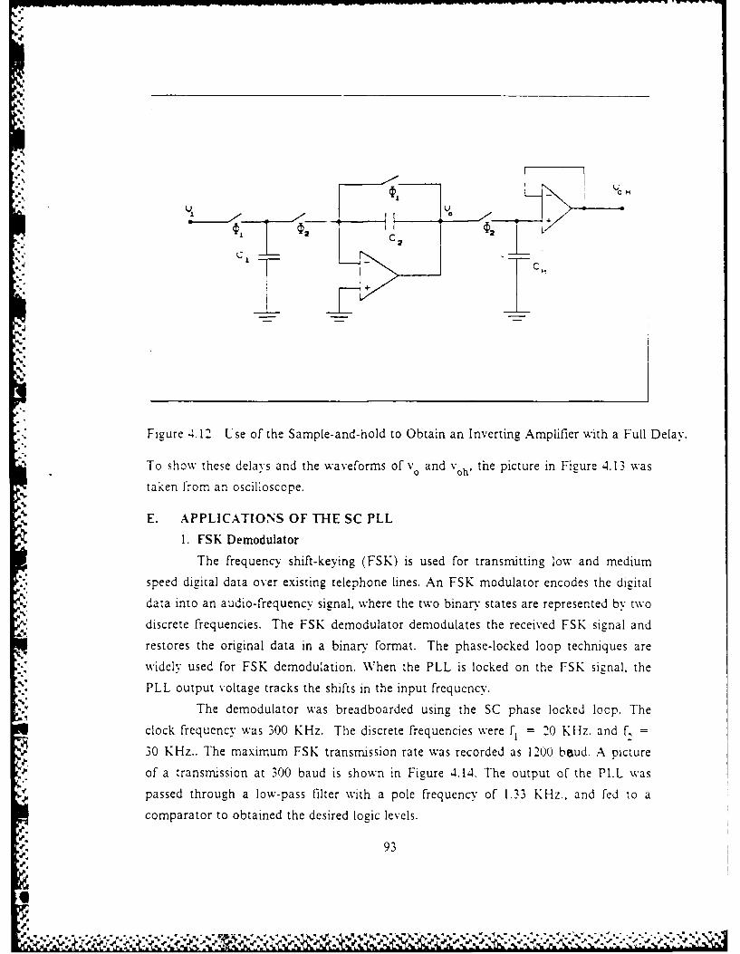
4."
t2 '0tknfo n silsoe
C 2
CI CM
-.Figure -4.12 Use of the Sample-and-hold to Obtain an Inverting Amplifier with a Full Delay.
To show these delavs and the waveforms of vo and v oh' the picture in Figure 4.13 was
taken from an oscilloscope.
E. APPLICATIONS OF THE SC PLL
1. FSK Demodulator
The frequency shift-keying (FSK) is used for transmitting low and medium
. speed digital data over existing telephone lines. An FSK modulator encodes the digital
data into an audio-frequency signal, where the two binary states are represented by two
discrete frequencies. The FSK demodulator demodulates the received FSK signal and
restores the original data in a binary format. The phase-locked loop techniques are
Nwidely used for FSK demodulation. When the PLL is locked on the FSK signal, the
-9' PLL output voltage tracks the shifts in the input frequency.
The demodulator was breadboarded using the SC phase locked loop. The
clock frequency was 300 KHz. The discrete frequencies were f1 = 20 KHz. and f, =
30 KHz.. The maximum FSK transmission rate was recorded as 1200 bBud. A picture
of a transmission at 300 baud is shown in Figure 4.14. The output of the PLL was
passed through a low-pass filter with a pole frequency of 1.33 Kttz., and fed to a
comparator to obtained the desired logic levels.
93
.;

Ficure '.I' ;a, Out'ut of the In,.ert ing Amplifier with a Half Delay,-" , Output Z), :he Sarnpie-and-h~old with a Ful -ea 250 "~ . 2 "oi 2 a ptsec div.).
' 2.Frequency SynthesisA freuency synithesizer can be built around a PLL as shown in igure '.I5 a
frec:uency d411. s inserted between the VCO output and the phase comnparator so_i "ha he loop signal to the comparator is at frequency fo while the VCO output is Nf .
!! .} This output is a multiple of the input Frequency as long as the loop is in lock. A digital
," '.4('
cc~untcr.,_ C-.., .;-was used as the frequency divider shown in Figure 4.9. 1f Q%, pin 6.~ ~ c -' ehe counter. is used as an input to the phase comparator, the comparator input... :-requ-,-cy will be a divide-by-16 from that of the V'CO output frequency. This wl
4Q
I~~i result in a r 4.1O aoutputto 16t fe the nrinp Ampifer withon as thalo eain
'.-.',94
2. FrqenySntei
Ahnuh
freuenv d€.d ,is nsete betwen .th.....utpu andth phas co. arto so . ...

(a)
Ficure .1~ at Binary Data Innut to be Modulatedb DeoduatedB~nrV Dta 5 Volts d..I rnsec div.).
*Input Phs
-SO

-AIS2 377 A SNITCHED-CAPACITOR PHASE-LOCKED LOOPCU) NAVAL 212POSTGRADUATE SCHOOL MONTEREY CA E OZGUNAY MAR 87
UNCLASSIFIED F/G 9/1 NLEhEm/EliIEEE|h
lii'.-M
W"~i hiM
1.2 111 .6
MICROCOPY RESOLUTION TEST CHARTNATIONAL BUREAU OF STANDARDS 1963-A
q I ro 7-
o.

3. Tracking Filter
SC filters have pole frequencies which are directly proportional to the clocking
frequency. It follows that the frequency response of a SC filter can be frequency scaled
by programming the frequency of the clock in the desired manner. This property is
used in the design of the tracking filter show in Figure 4.16, [Ref. 9].
InputtSignali
Ttp ched capa ior ilte s Output
w i th pc t frequency. t It -%t me € I OCk freqey
Figure 4.16 Block Diagram of a Tracking Filter.
The input signal is fed both to a phase-locked loop as well as to the SC filte.When the PLL locks onto the input signal, the VCO frequency will be exactly N timesthe input frequency. The VCO output is used to drive the switches of the ilter which isdesigned to have a pole frequency equal to (1l/N) times the clocking frequency. Itfollows that the pole frequency of the filter %%ill be equal to the frequency of the input
signal, provided that the phase-locked loop is in lock.
The switched capacitor filter can be designed to have any desired function
(e.g., bandpass, low pass, etc.) as well as any desired order. A discrete prototype of the
circuit of Figure 4.16 was built and the PLL circuit of Figure 3.15 was used in Figure
4.17. The divide-by-N circuit was chosen as a divide-by-16 by using the Q4. output of
the binary counter, CD4024.
96
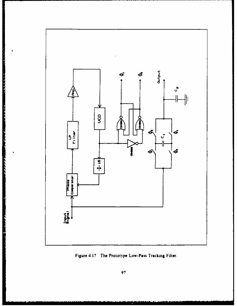
CL
00
Figure 4.17 The Prototype Low-Pass Tracking Filter.
97

A first order SC low-pass filter was constructed using the bilinear SC
realization. From Equation 2.1 the pole frequency is given w - I - I R C,rad sec.
r, - 2nRIC 2 Iz..
If the bilinear SC realization is used for the continuous resistor. R. the pole frequency
. becomes
't Cf- 'C - (.4.13)
it C 2
Since f - 16 f1' Equation .4.13 becomes
32 C
C it
C, 32
provided that fl - fi. If the PLL is in lock, one can always obtain pole frequency
attenuation of I ,2 and a phase shift of 45 degrees at the filter output since a first
order low-pass filter is used.
In the experiment C,- I nF, and C2- 10 nF. The output phase and
magnitude of the SC filter was observed to remain constant irrespective of the input
frequency between I KHz. and 6.5 Kliz. The waveforms of Figure 4.17 are shown in
Figure 4.18 and Figure 4.19 for a 4 KlIz. and 6.25 KHz. for sinusoidal input signal.
respectis ely. The filter output had the same pole frequency attenuation and a 45 degree
phase shift.
98

Figure .4.13S The I nrut and tht Output Waveforms of the Figure 41.1".f-K Hz. (I Volt div.. 20 jasec div.)
Figure .4.19 The In~yt ?Ad.the Qtut waveforms of the Figure .4. 1".6. -3 Kz ( 1,oltdiv.. 20 psec div..
99

V. CONCLUSION
In this thesis research the resistors of an RC network were replaced by the
switched capacitor (SC) networks, resulting in a sampled data equivalent network.
Many of the switched capacitor networks described in the literature have been either
for filtering or analog-to-digital conversion applications. SC networks are also useful
for realizing many other signal processing functions. In the research some of the SC
building blocks, useful in realizing adaptive systems, were described as well as some
passive RC filter applications.
As stated in the abstract, it was shown that the switched capacitor resistors were
exactly equivalent to resistors by themselves, however, such an equivalence might not
hold true when the realizations were used to replace resistors of an RC active network
due to the discrete-time nature of SC networks. It was also shown that it was
technologically possible to include digital circuitry along with SC networks in the same
IC network.
During the research, first, the types of realization methods and tneir properties
were discussed. Furthermore. some of the main SC building blocks were presented such
as a voltage controlled oscillator (VCO), an amplifier, and a hard liniter. These
building blocks led to the design of a more complicated SC circuit, a phase-locked loop
(PLL). First, an analog version of the PLL was breadboarded. then, it was converted to
a switihed capacitor PLL using the realization methods mentioned before.
Experiments showed that the clock frequency should be an integer multiple of the
oscillation frequency. For this reason the sampling ratio was kept rather high in order
to nuninuze the phase jitter. This was the major limitation on the SC PLL design. To
avoid this restriction, the SC VCO was replaced by its analog version. resulting in a
hybrid phase-locked loop. (Ref 101. The results obtained from the hybrid version were
very close to the analog version ones. The hybrid circuit using SC network technology."4 also had the advantages such as accuracy, practical implementation. and lower cost.
In the design mostly MOS switches. MOS amplifiers, and MOS digital circuits were
used to take adsantages of the NIOS technology and probable further VLSI design of
the circuit.
100
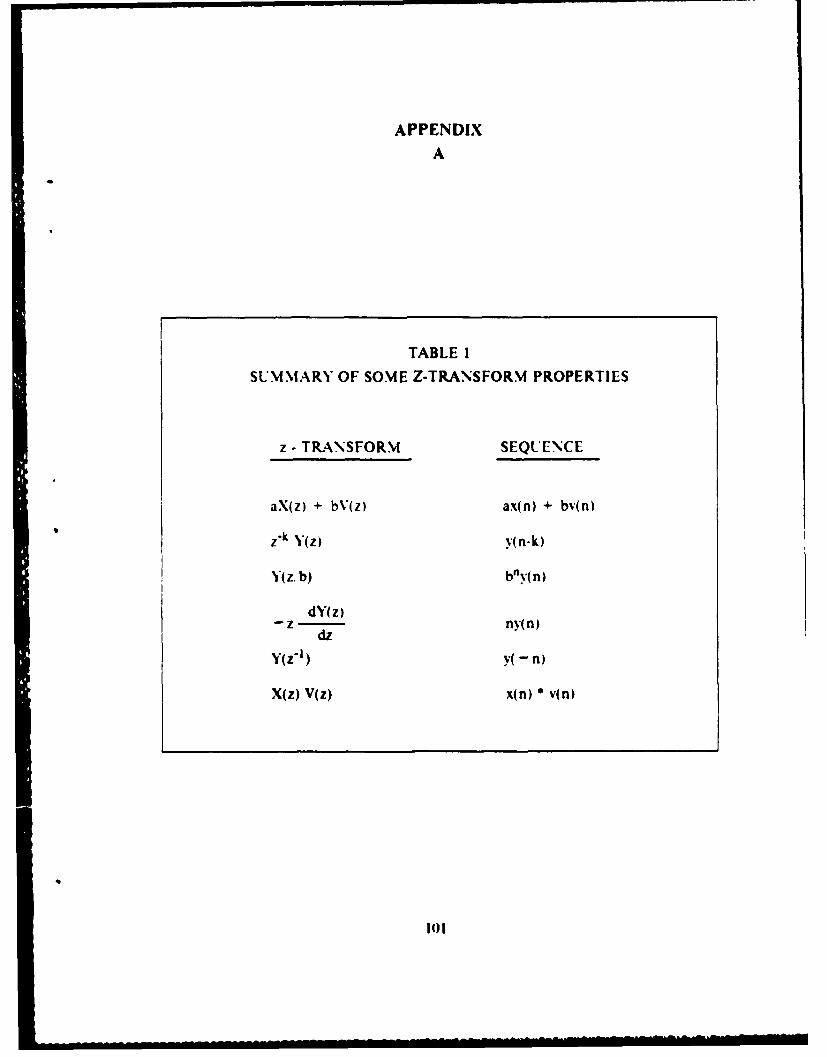
APPENDIXA
TABLE I
SUMMARY OF SOME Z-TRANSFORM PROPERTIES
z - TRANSFORM SEQUENCE
aX(z) + b%*(z) ax(n) +- b'dn)
Z'k Y(Z) y(n-k)
Y(z, b) b n
zdY(z) yndz
Y(z'I) y(- n)
X(Z) V(Z) x(n) * v(n)
t0t
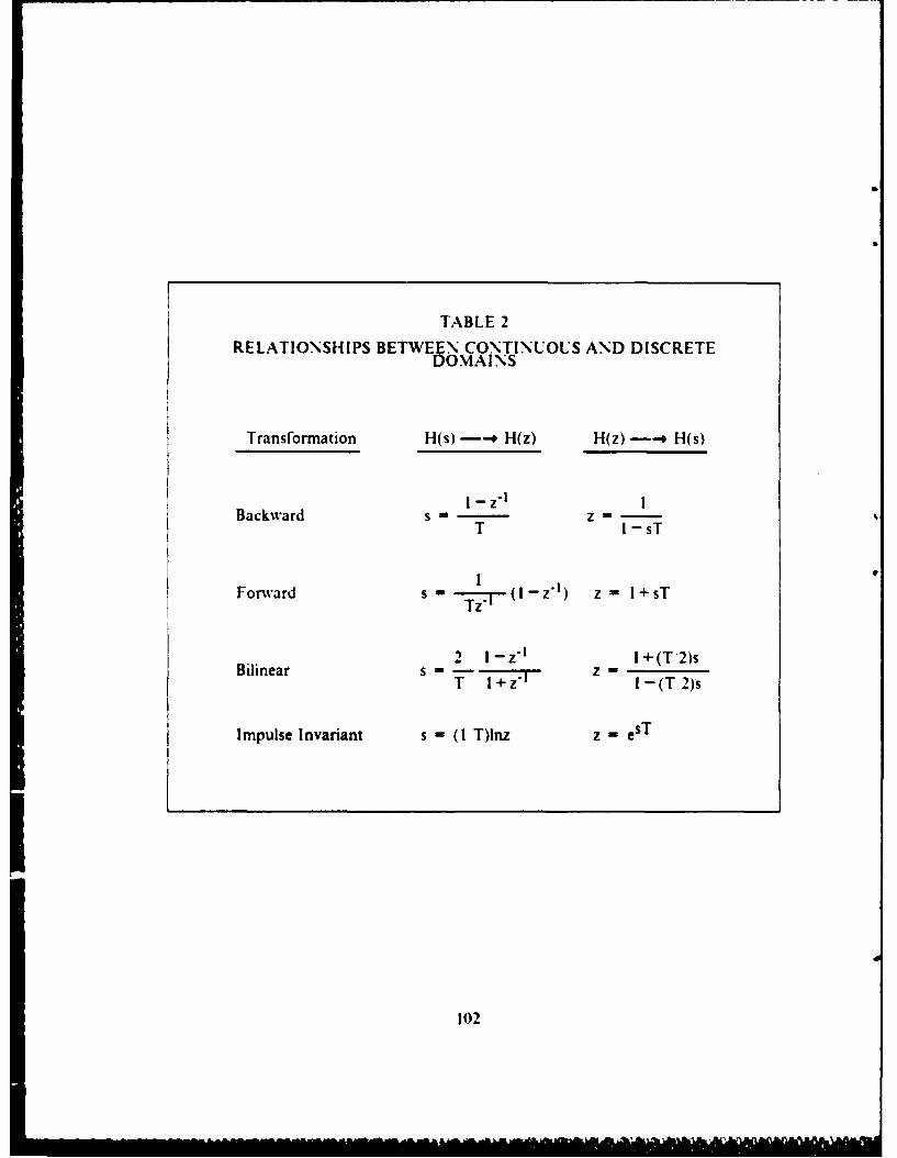
TABLE 2
RELATIONSHIPS BETWEEN CONTINUOUS AND DISCRETEDOMAINS
Transformation H(s) -- # H(z) H(z) -.. H(s)
Backward s Z =T I-sT
IForward s 1 -(i-z " ) z - I+sT
2 I-z "1 I+(T2)sBilinear S - Z -
T + -(T 2)s
Impulse Invariant s = (I T)lnz z = sT
102

LIST OF REFERENCES
I. Ghausi. M. S. and Laker. K. R., Modern Filter Design, Prentice-Hall, Inc., 1981.
2. Sanchez. S.E. and Allen. F. E., Switched Capacitor Circuits, Van NostrandReinhold Comp. Inc.. 1984.
3. Irvine R G Operational Amplifier Characteristics and Applications, Prentice-Flail, Inc., 1 1.
4. Tsividis. Y. P.. "Analysis of Switched Capacitive Networks.," Proc. of the 1979 Int.Symp. on Circuits and Systems, ISCAS, pp. 752-755, Jul 0q79.
5. Young, T., Linear Integrated Circuits, John Wiley &Sons, Inc., 1981.
6. Blanchard, A., Phase-Locked Loops. John Wiley & Sons, Inc., 1976.
7. Lindsey, W. C. and Chie, C. M., Phase-Locked Loops, IEEE Press Book, page 17,1986.
S. .Martin K "A Voltage-Controlled Switched-Capacitor Relexation Oscillator,"IEEE J. Solid-State Cijcuits, Vol. SC-16, pp. 412-414, Aug. 1981.
9. Martin, K. and Sedra, A. S., "Switched-Capacitor Building Blocks for AdaptiveSystems," IEEE Transactions on Circuits and Systems, Vor. CAS-28, No. 6, pp.i76-5S4. Jun. 1981.
10. Asta. D.. "A Novel Hybrid Analo% Switched-Capacitor Phase-Locked LoopSystem and Circuit Desiin." DISS. ABST. INT. PF. B-SCI&ENG., Vol. 46, No.7' Univ. California, Los Angeles, CA, Jan. 1986.
103

INITIAL DISTRIBUTION LIST
No. Copies
1. Defense Technical Information Center 2Cameron StationAlexandria, Virginia 22304-6145
2. Library Code 0142 2Naval *ost~raduate SchoolMonterey, California 93943-5002
3. Turkish Navv General Staff 4Bakanliklar, -Ankara Turkey
4. Professor Sherif Michael. Code 62Mi 4Naval Postgraduate SchoolMonterey, California 93943
5. Professor Roberto Cristi. Code 62Cx 2Naval Postgraduate SchoolMonterey, California 93943
6. Department Chairman Code 62 2Naval Postgraduate SchoolMonterey, California 93943
7. LTJG. E. Ozgunav- Turkish Navy. 6Icadive Mahallesi. kurtcelebi sokak, No:55'I,Bazldrbasi Uskudar,Ist~nbul, Turkey
104

W"W4-