Embed Size (px)
DESCRIPTION
More Basics of CPU Design. Lecture for CPSC 5155 Edward Bosworth, Ph.D. Computer Science Department Columbus State University. Design of a CPU. This lecture covers topics basic to the design of a modern CPU, including that of the MIPS. - PowerPoint PPT Presentation
Citation preview
More Basicsof
CPU DesignLecture for CPSC 5155
Edward Bosworth, Ph.D.Computer Science Department
Columbus State University
Design of a CPU
• This lecture covers topics basic to the design of a modern CPU, including that of the MIPS.
1. The storage elements used to save data and to save the execution state.
2. The flow of data through the CPU.3. The control signals that control the CPUSome slides in this lecture will be based on an earlier design (the Boz-5) by your instructor.
3
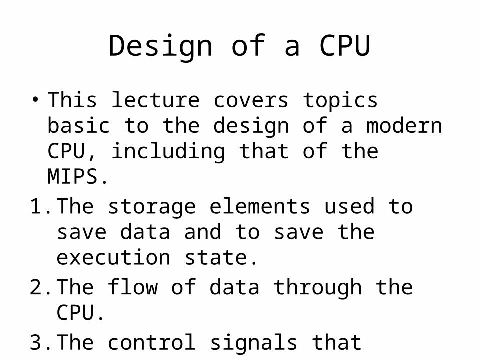
Components of a Stored Program Computer
The von Neumann Design
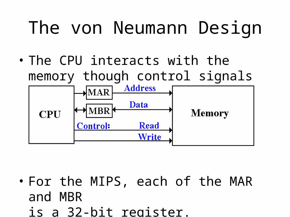
• The CPU interacts with the memory though control signals and two registers.
• For the MIPS, each of the MAR and MBRis a 32-bit register.
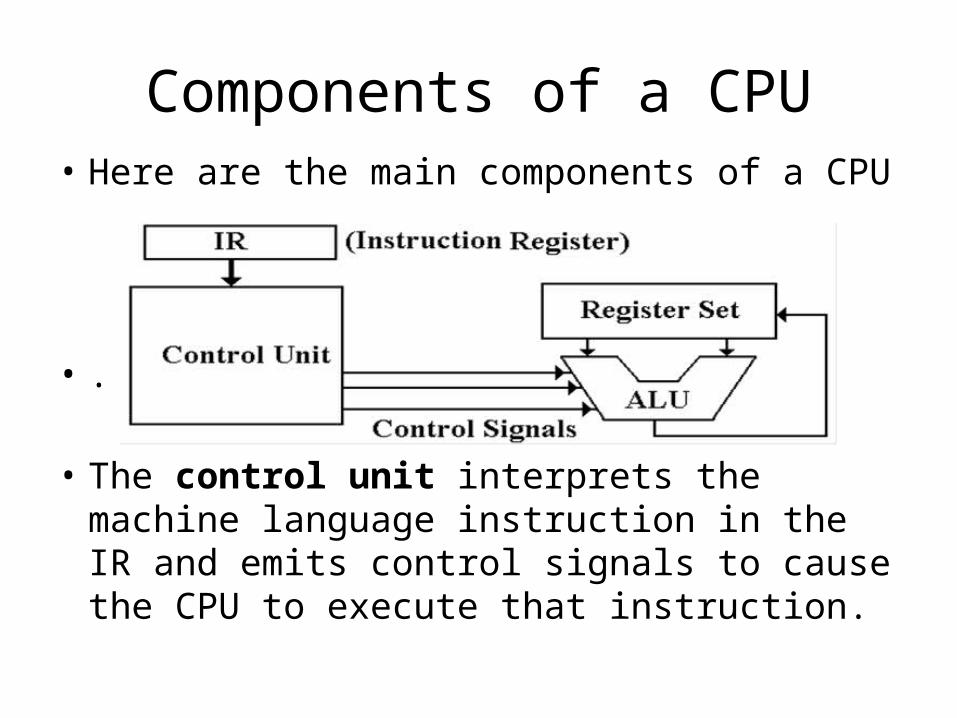
Components of a CPU• Here are the main components of a CPU
• .
• The control unit interprets the machine language instruction in the IR and emits control signals to cause the CPU to execute that instruction.
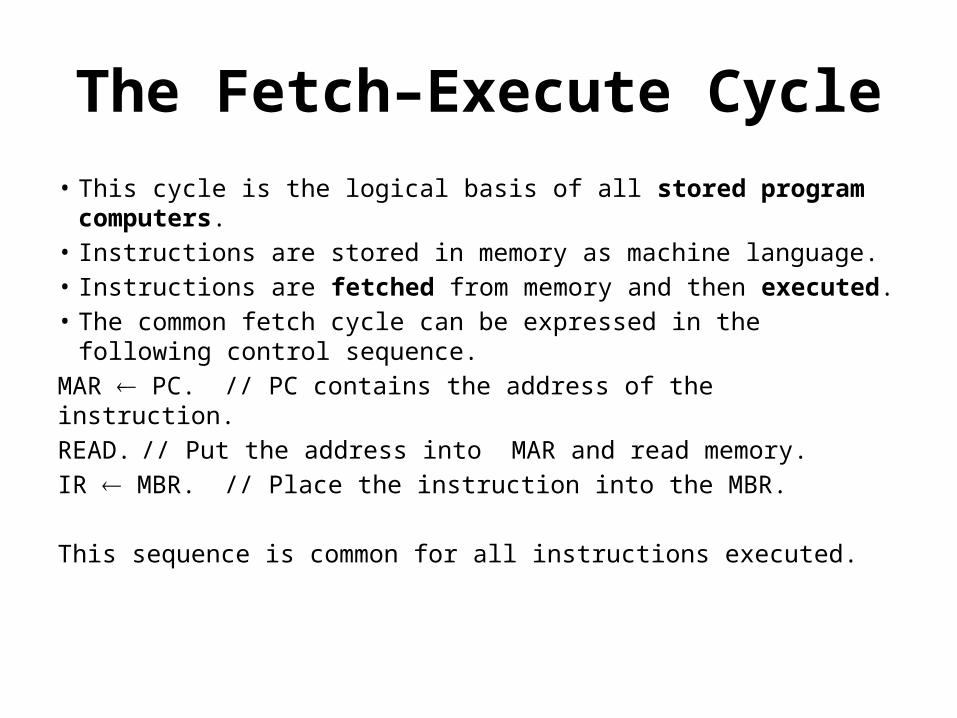
The Fetch–Execute Cycle• This cycle is the logical basis of all stored program computers.• Instructions are stored in memory as machine language.• Instructions are fetched from memory and then executed.• The common fetch cycle can be expressed in the following
control sequence.MAR PC. // PC contains the address of the instruction.READ. // Put the address into MAR and read memory.IR MBR. // Place the instruction into the MBR.
This sequence is common for all instructions executed.
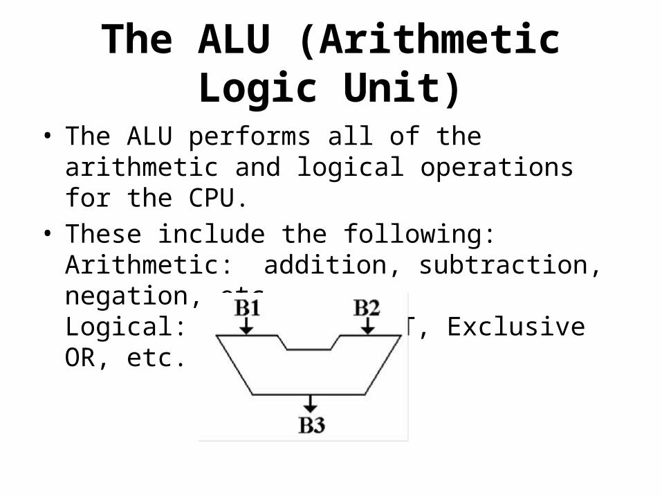
The ALU (Arithmetic Logic Unit)
• The ALU performs all of the arithmetic and logical operations for the CPU.
• These include the following:Arithmetic: addition, subtraction, negation, etc.Logical: AND, OR, NOT, Exclusive OR, etc.
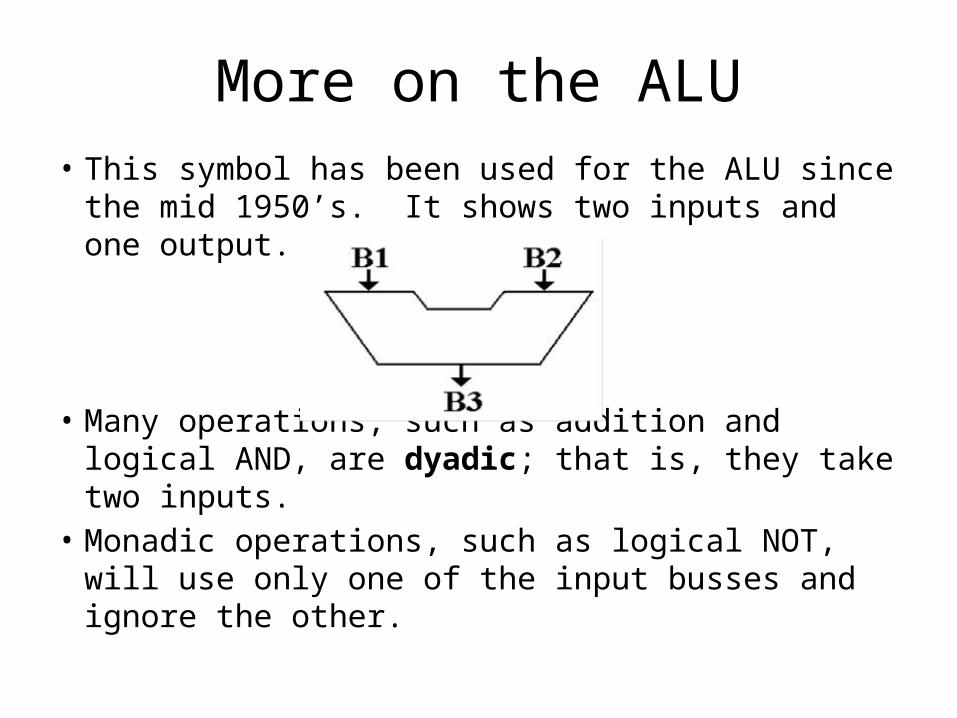
More on the ALU• This symbol has been used for the ALU since the
mid 1950’s. It shows two inputs and one output.
• Many operations, such as addition and logical AND, are dyadic; that is, they take two inputs.
• Monadic operations, such as logical NOT, will use only one of the input busses and ignore the other.
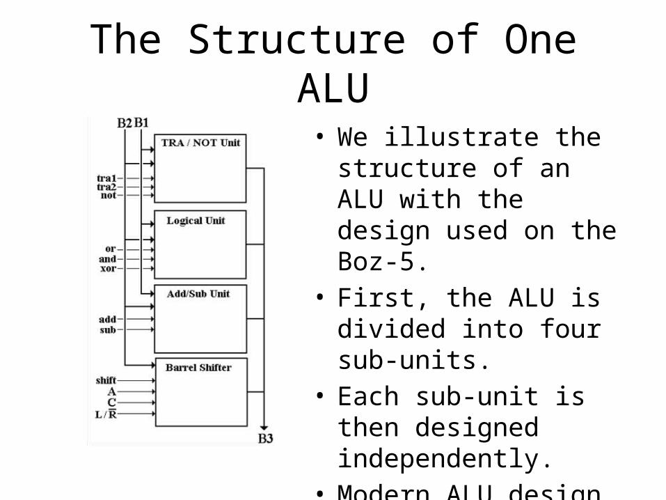
The Structure of One ALU
• We illustrate the structure of an ALU with the design used on the Boz-5.
• First, the ALU is divided into four sub-units.
• Each sub-unit is then designed independently.
• Modern ALU design is somewhat different.
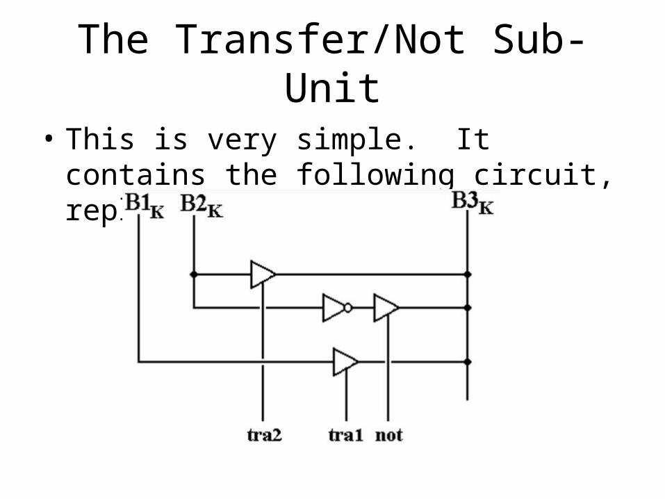
The Transfer/Not Sub-Unit
• This is very simple. It contains the following circuit, replicated 32 times.
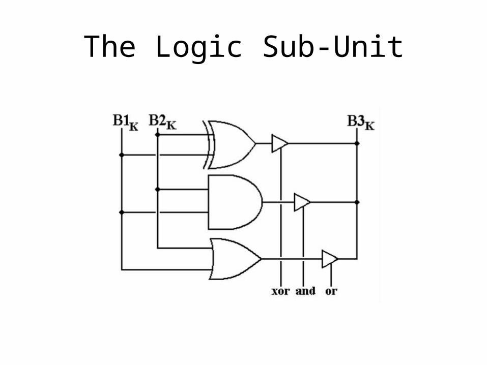
The Logic Sub-Unit
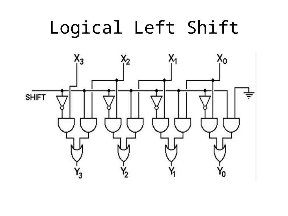
Logical Left Shift
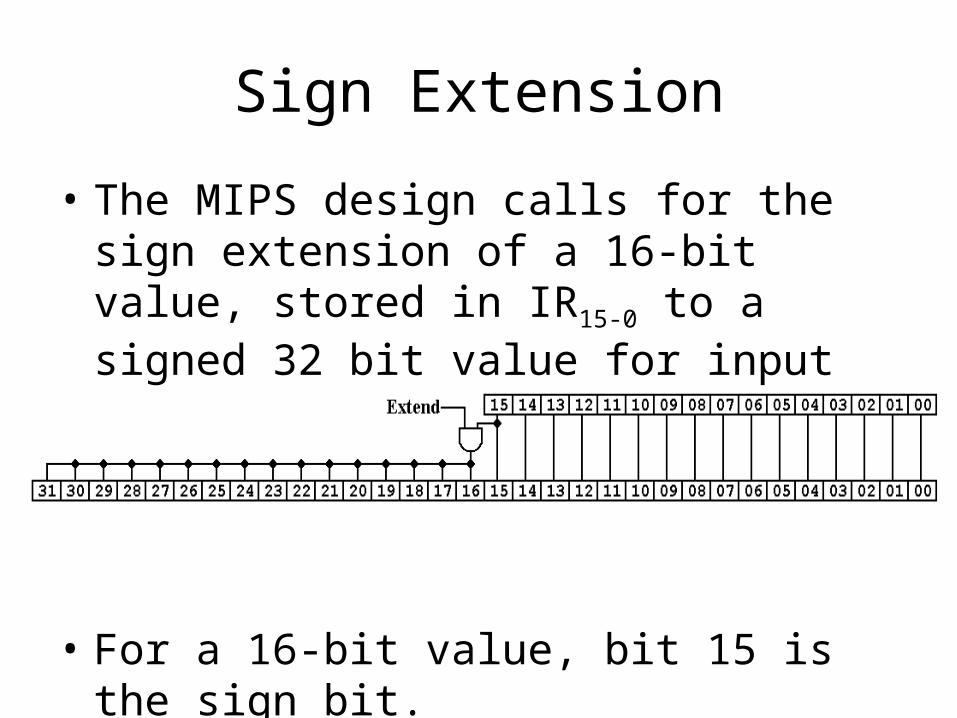
Sign Extension
• The MIPS design calls for the sign extension of a 16-bit value, stored in IR15-0 to a signed 32 bit value for input to the ALU
• For a 16-bit value, bit 15 is the sign bit.For a 32-bit value, bit 31 is the sign bit.
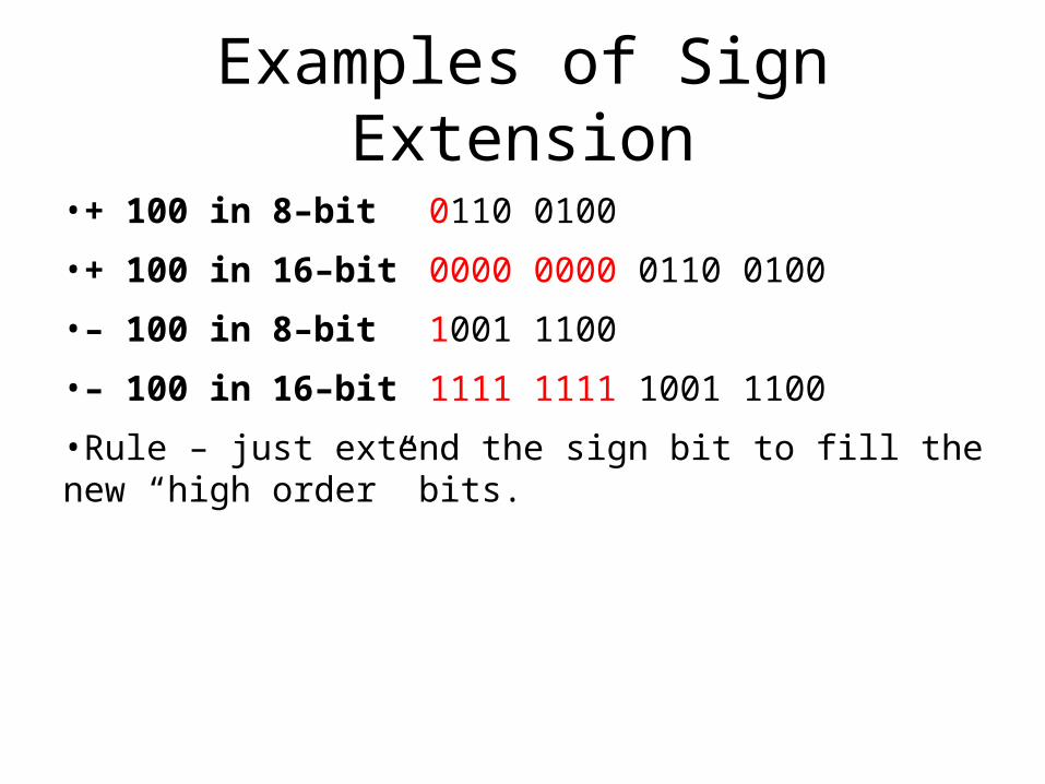
Examples of Sign Extension•+ 100 in 8–bit 0110 0100
•+ 100 in 16–bit 0000 0000 0110 0100
•– 100 in 8–bit 1001 1100
•– 100 in 16–bit 1111 1111 1001 1100
•Rule – just extend the sign bit to fill the new “high order” bits.
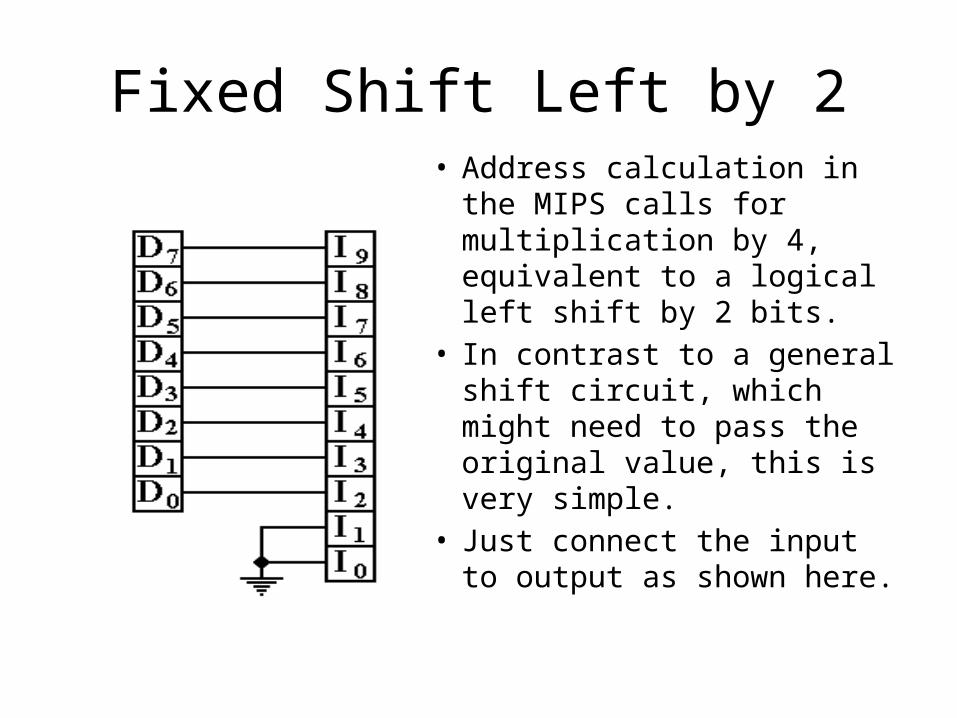
Fixed Shift Left by 2• Address calculation in the
MIPS calls for multiplication by 4, equivalent to a logical left shift by 2 bits.
• In contrast to a general shift circuit, which might need to pass the original value, this is very simple.
• Just connect the input to output as shown here.
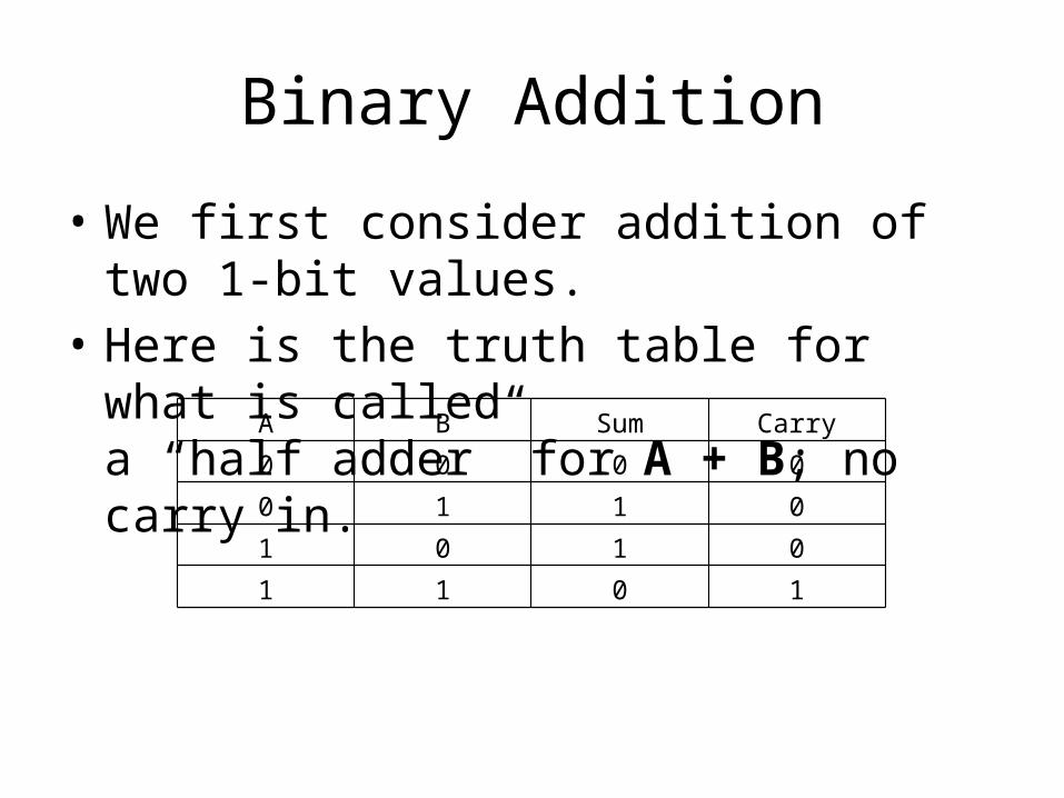
Binary Addition
• We first consider addition of two 1-bit values.• Here is the truth table for what is called
a “half adder” for A + B; no carry in.A B Sum Carry0 0 0 00 1 1 01 0 1 01 1 0 1
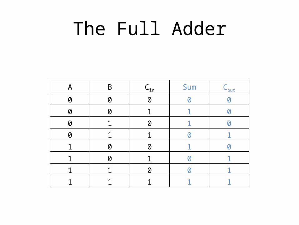
The Full Adder
A B Cin Sum Cout
0 0 0 0 00 0 1 1 00 1 0 1 00 1 1 0 11 0 0 1 01 0 1 0 11 1 0 0 11 1 1 1 1
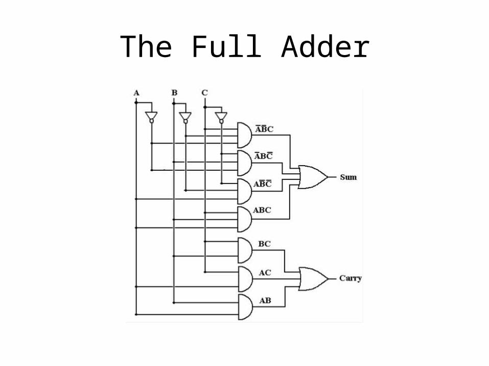
The Full Adder
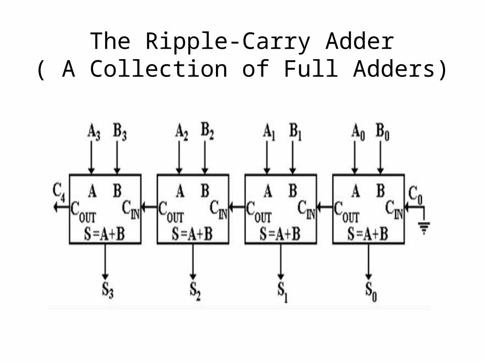
The Ripple-Carry Adder( A Collection of Full Adders)
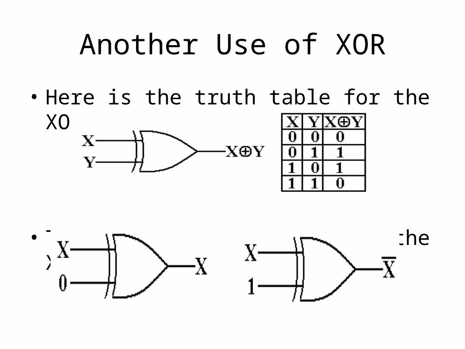
Another Use of XOR
• Here is the truth table for the XOR gate.
• This illustrates one use of the XOR gate.
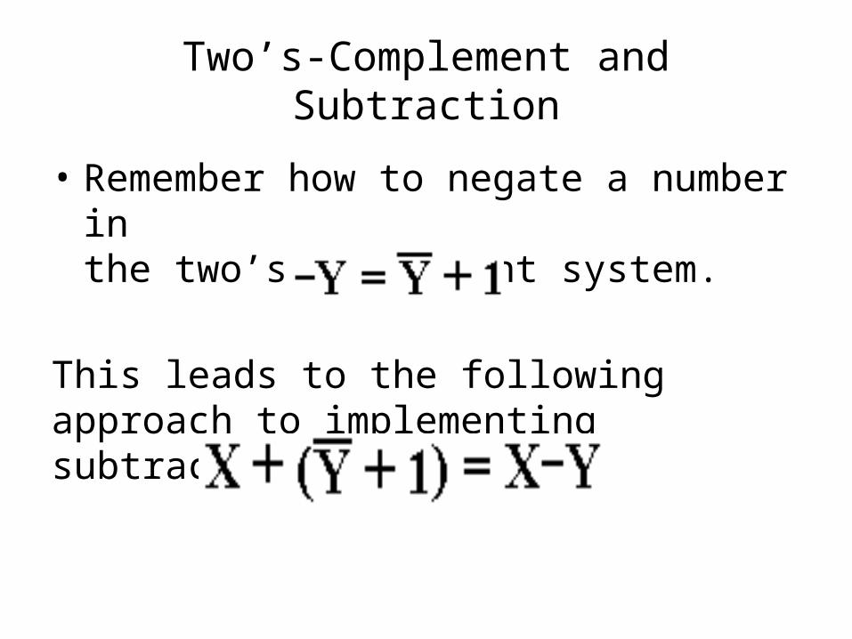
Two’s-Complement and Subtraction
• Remember how to negate a number in the two’s-complement system.
This leads to the following approach to implementing subtraction
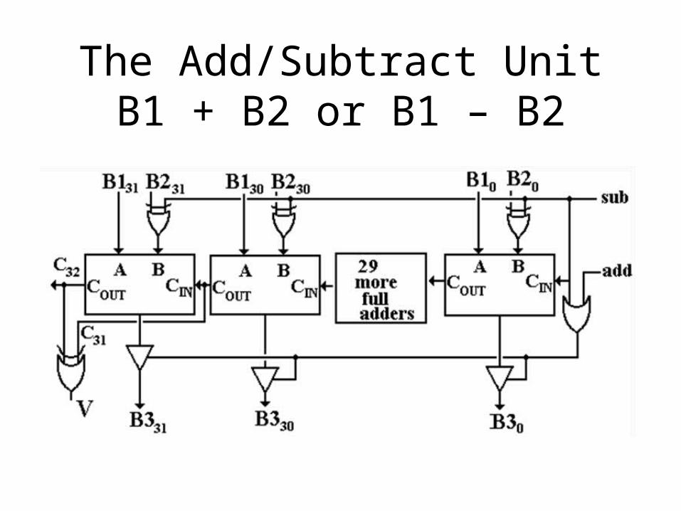
The Add/Subtract UnitB1 + B2 or B1 – B2
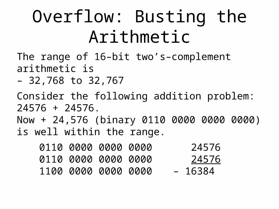
Overflow: Busting the Arithmetic
The range of 16–bit two’s–complement arithmetic is– 32,768 to 32,767Consider the following addition problem: 24576 + 24576.Now + 24,576 (binary 0110 0000 0000 0000) is well within the range.
0110 0000 0000 0000 245760110 0000 0000 0000 245761100 0000 0000 0000 – 16384
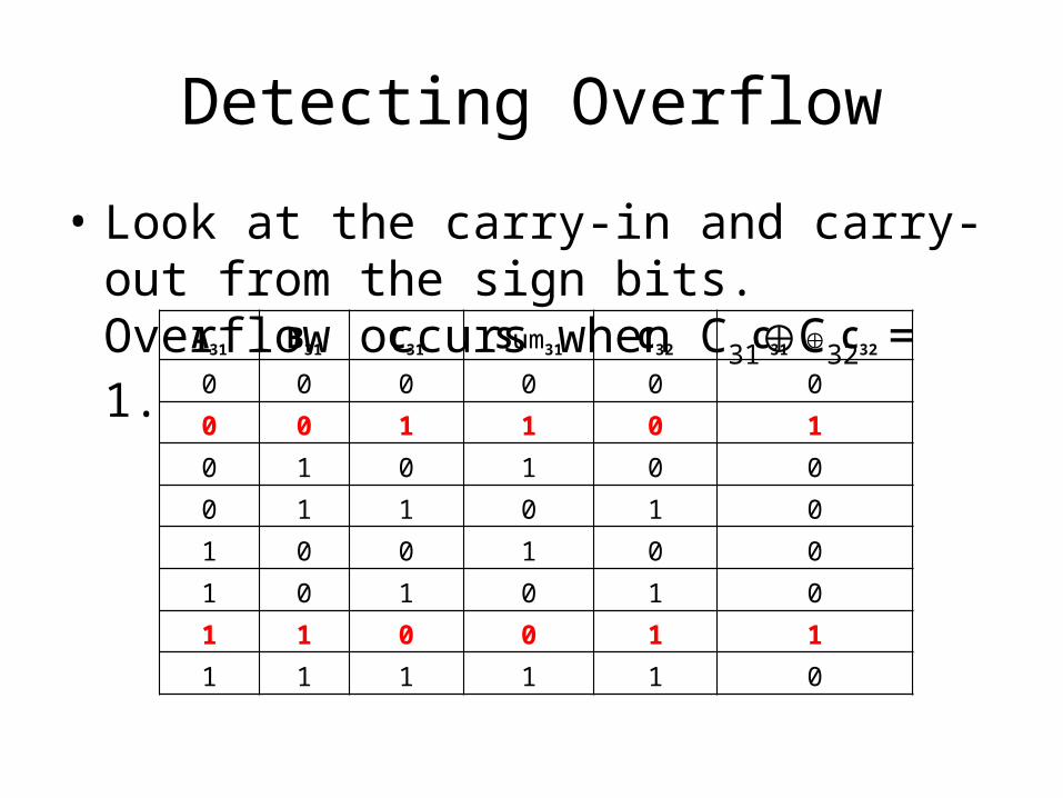
Detecting Overflow
• Look at the carry-in and carry-out from the sign bits. Overflow occurs when C31C32 = 1.
A31 B31 C31 Sum31 C32 C31 C32
0 0 0 0 0 00 0 1 1 0 10 1 0 1 0 00 1 1 0 1 01 0 0 1 0 01 0 1 0 1 01 1 0 0 1 11 1 1 1 1 0
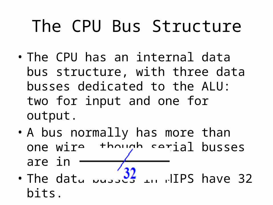
The CPU Bus Structure
• The CPU has an internal data bus structure, with three data busses dedicated to the ALU: two for input and one for output.
• A bus normally has more than one wire, though serial busses are in use.
• The data busses in MIPS have 32 bits.
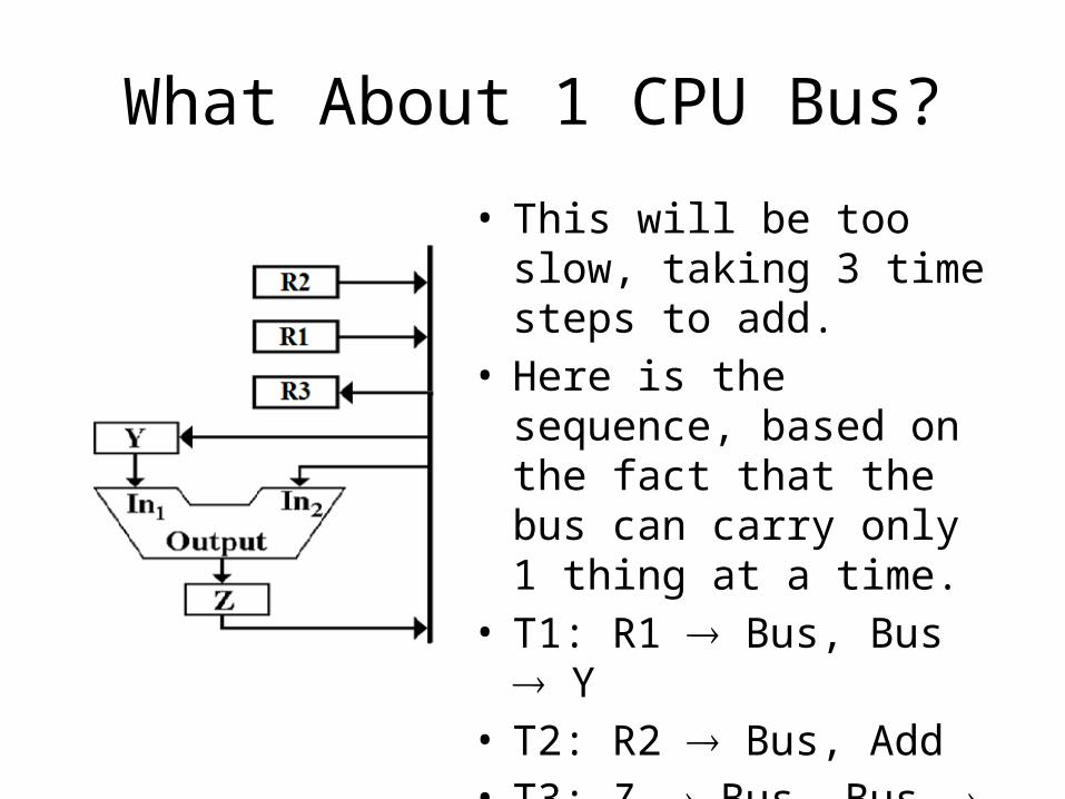
What About 1 CPU Bus?
• This will be too slow, taking 3 time steps to add.
• Here is the sequence, based on the fact that the bus can carry only 1 thing at a time.
• T1: R1 Bus, Bus Y• T2: R2 Bus, Add• T3: Z Bus, Bus R3.
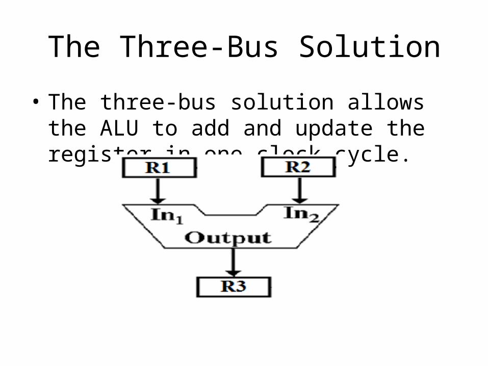
The Three-Bus Solution
• The three-bus solution allows the ALU to add and update the register in one clock cycle.
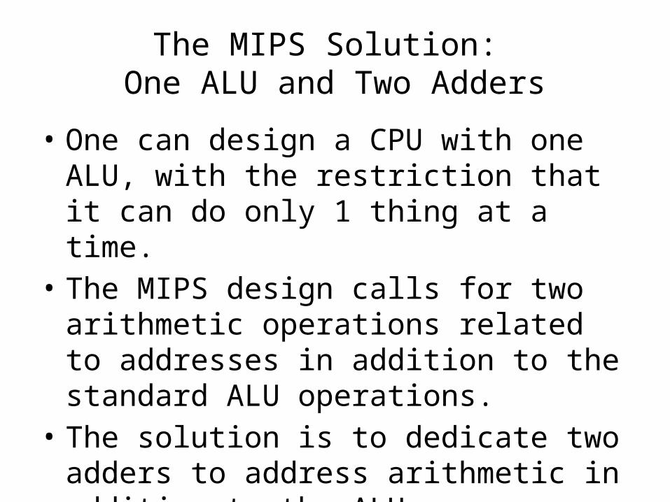
The MIPS Solution: One ALU and Two Adders
• One can design a CPU with one ALU, with the restriction that it can do only 1 thing at a time.
• The MIPS design calls for two arithmetic operations related to addresses in addition to the standard ALU operations.
• The solution is to dedicate two adders to address arithmetic in addition to the ALU.
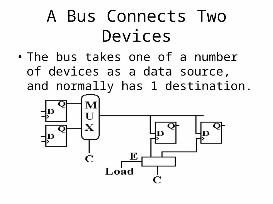
A Bus Connects Two Devices
• The bus takes one of a number of devices as a data source, and normally has 1 destination.
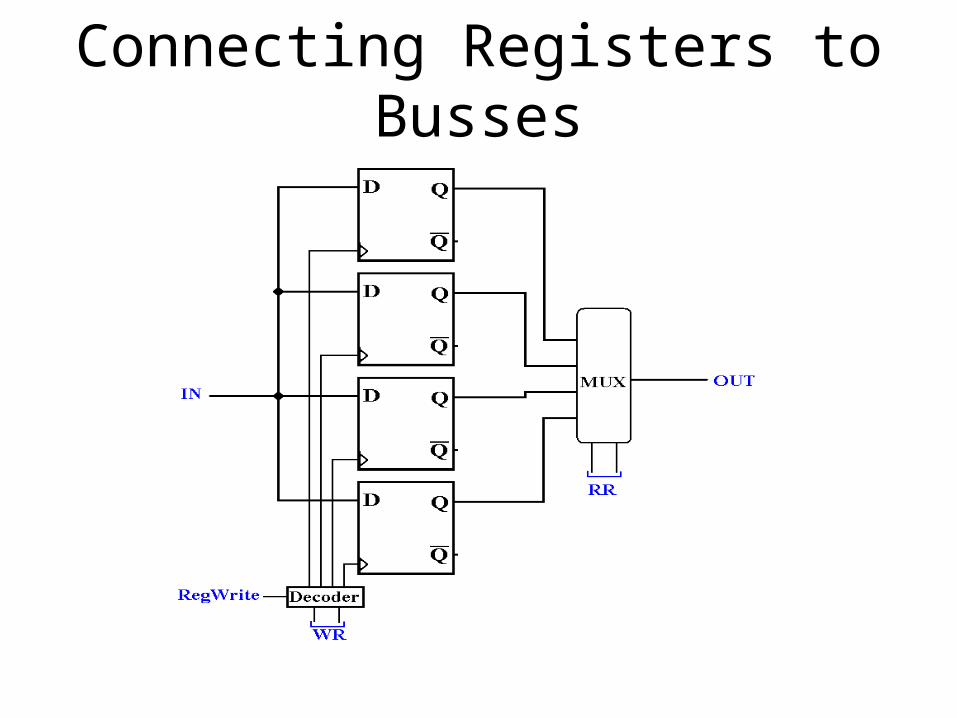
Connecting Registers to Busses
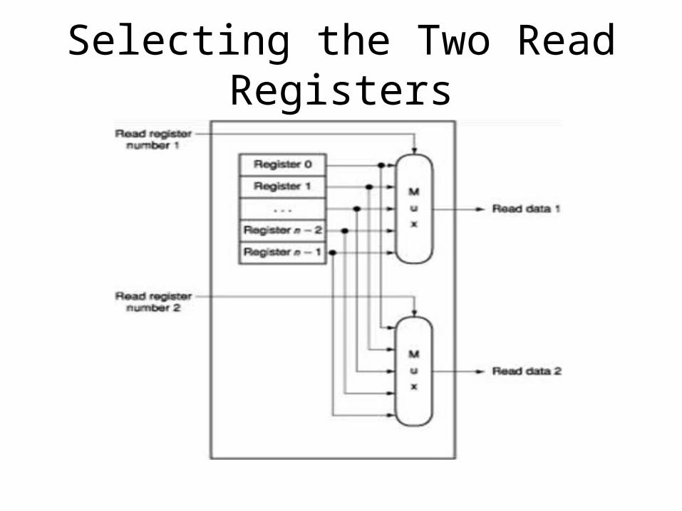
Selecting the Two Read Registers
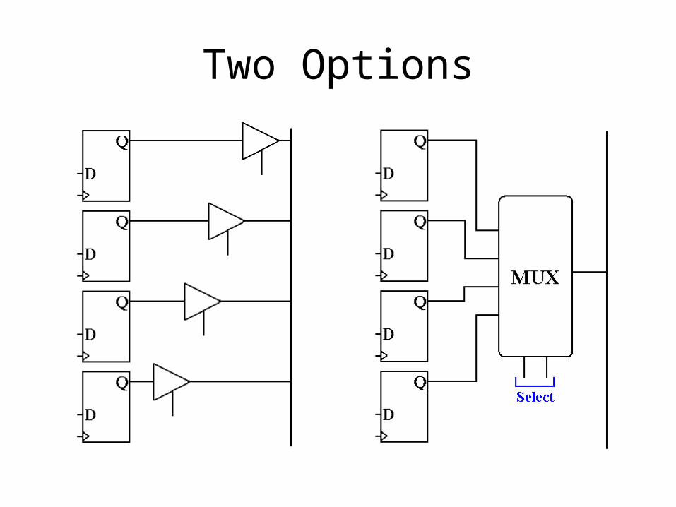
Two Options
Chapter 4 — The Processor — 33
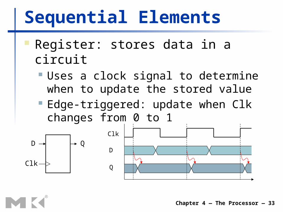
Sequential Elements Register: stores data in a circuit
Uses a clock signal to determine when to update the stored value
Edge-triggered: update when Clk changes from 0 to 1
D
Clk
QClk
D
Q
Chapter 4 — The Processor — 34
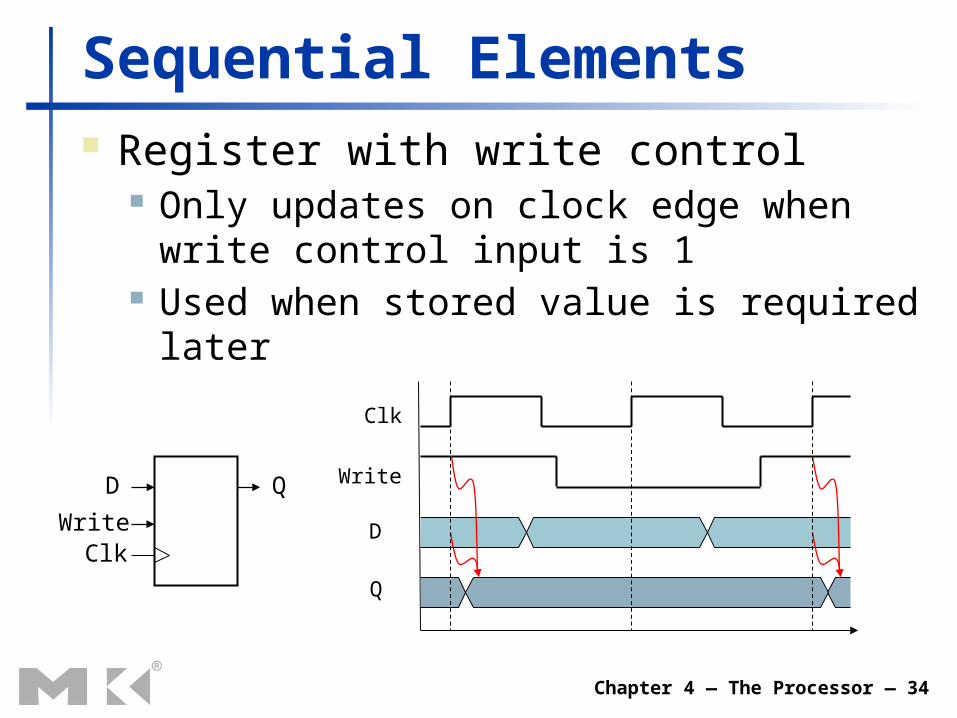
Sequential Elements Register with write control
Only updates on clock edge when write control input is 1
Used when stored value is required later
D
Clk
QWrite
Write
D
Q
Clk
Chapter 4 — The Processor — 35
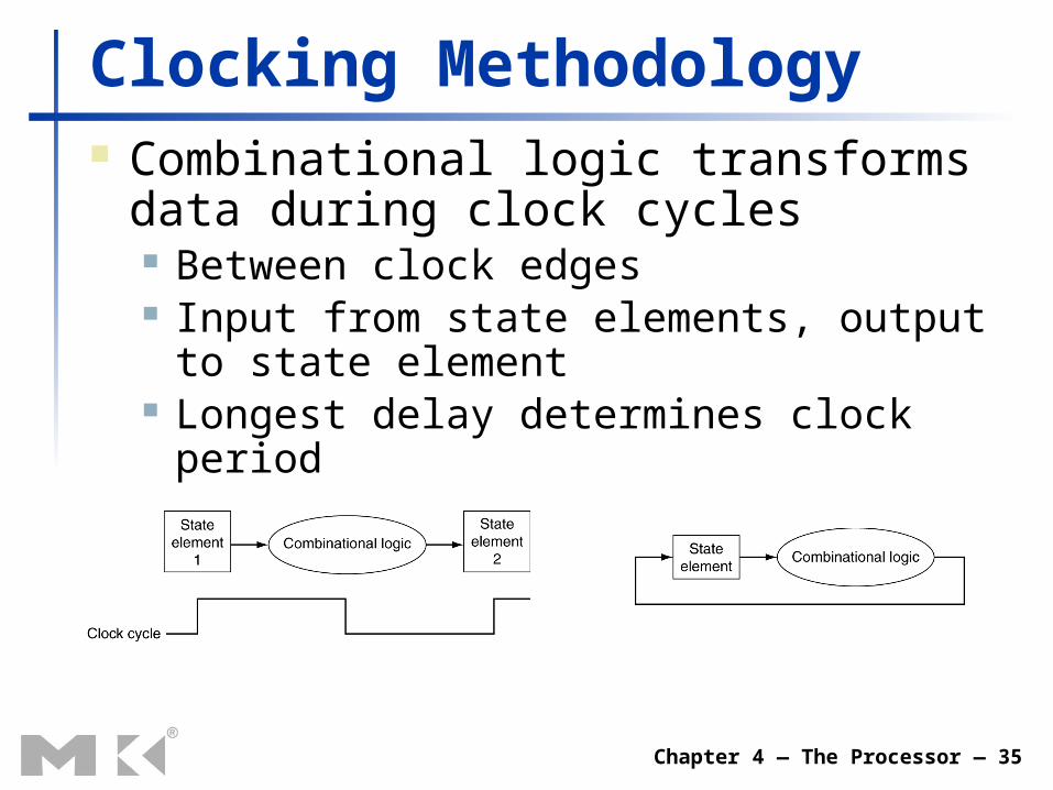
Clocking Methodology Combinational logic transforms data during
clock cycles Between clock edges Input from state elements, output to state
element Longest delay determines clock period
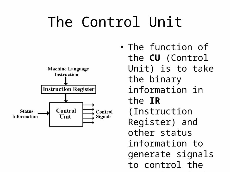
The Control Unit
• The function of the CU (Control Unit) is to take the binary information in the IR (Instruction Register) and other status information to generate signals to control the execution of the program in the computer.
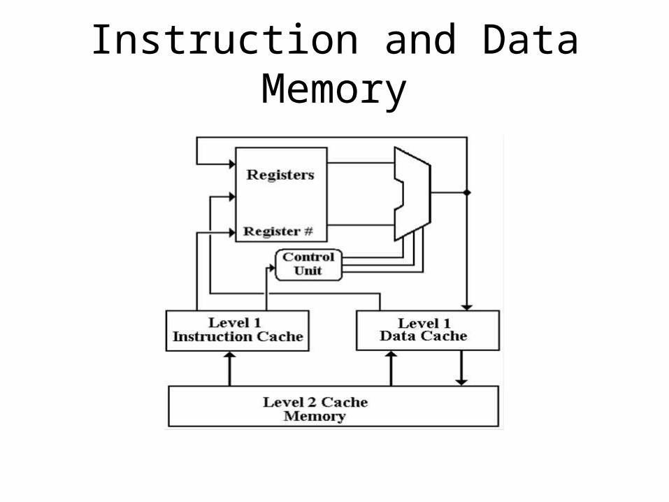
Instruction and Data Memory