Embed Size (px)
Citation preview

MOS-AK 2005 8 avril 2005
CMOS compatible integrated magnetometers
L. Hébrard1, J.-B. Kammerer1, M. Hehn2, V. Frick1,
A. Schuhl2, P. Alnot3, P. French4, F. Braun1
1 InESS - 2 LPM (UHP-Nancy) - 3 LPMI (UHP-Nancy) - 4 EIL (TU-Delft -The Netherlands)
MOS-AK - 2005 Page 2/19Strasbourg 8 avril 2005
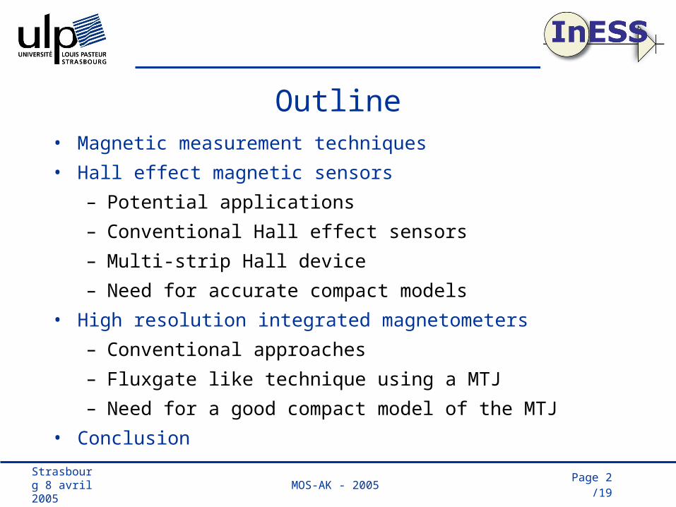
Outline• Magnetic measurement techniques
• Hall effect magnetic sensors
– Potential applications
– Conventional Hall effect sensors
– Multi-strip Hall device
– Need for accurate compact models
• High resolution integrated magnetometers
– Conventional approaches
– Fluxgate like technique using a MTJ
– Need for a good compact model of the MTJ
• Conclusion
MOS-AK - 2005 Page 3/19Strasbourg 8 avril 2005
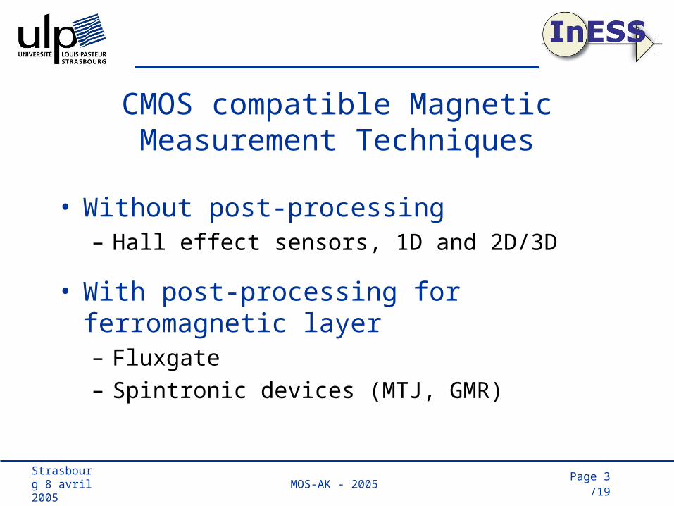
CMOS compatible Magnetic Measurement Techniques
• Without post-processing– Hall effect sensors, 1D and 2D/3D
• With post-processing for ferromagnetic layer– Fluxgate– Spintronic devices (MTJ, GMR)
MOS-AK - 2005 Page 4/19Strasbourg 8 avril 2005
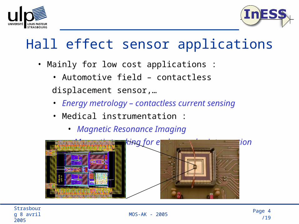
Hall effect sensor applications• Mainly for low cost applications :
• Automotive field – contactless displacement sensor,
…
• Energy metrology – contactless current sensing
• Medical instrumentation :
• Magnetic Resonance Imaging
• Magnetic tracking for endovascular intervention
MOS-AK - 2005 Page 5/19Strasbourg 8 avril 2005
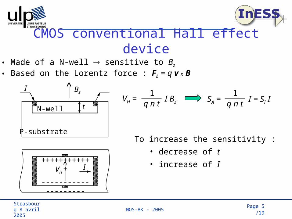
CMOS conventional Hall effect device
• Made of a N-well sensitive to Bz • Based on the Lorentz force : FL = q v x B
P-substrate
Bz
++++++++++++
--------------------
IVH
VH =1
q n tI Bz
1q n t
SA = I = SI IN-well
To increase the sensitivity :
• decrease of t
• increase of I
I
t
MOS-AK - 2005 Page 6/19Strasbourg 8 avril 2005
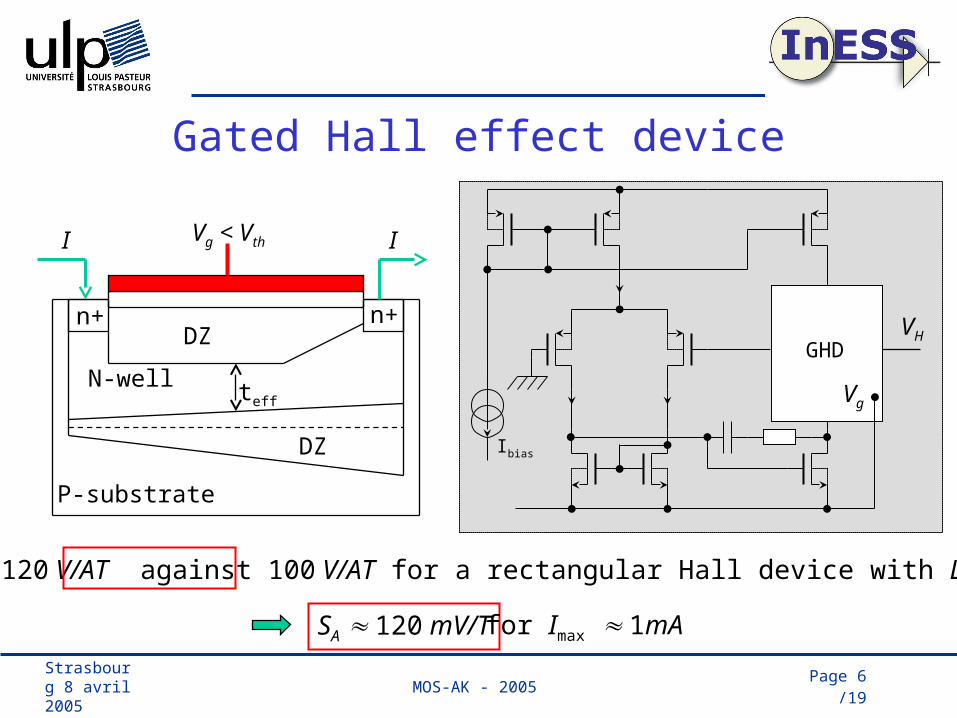
Gated Hall effect device
n+n+
P-substrate
DZ
N-well
II
teff
DZ
Vg < Vth
Ibias
VH
Vg
GHD
SI = 120 V/AT against 100 V/AT for a rectangular Hall device with L/W ≥ 3
SA 120 mV/T for Imax 1mA
MOS-AK - 2005 Page 7/19Strasbourg 8 avril 2005
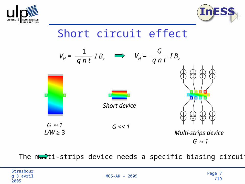
Short circuit effect
The multi-strips device needs a specific biasing circuit
G 1L/W ≥ 3 Multi-strips device
G 1
Short device
G << 1
VH =G
q n tI BzVH =
1q n t
I Bz
MOS-AK - 2005 Page 8/19Strasbourg 8 avril 2005
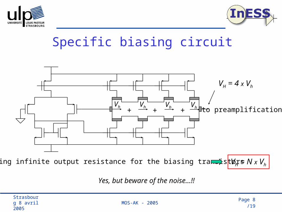
Specific biasing circuit
to preamplification+ + +Vh Vh Vh Vh
VH = 4 x Vh
VH = N x VhAssuming infinite output resistance for the biasing transistors
Yes, but beware of the noise…!!
MOS-AK - 2005 Page 9/19Strasbourg 8 avril 2005
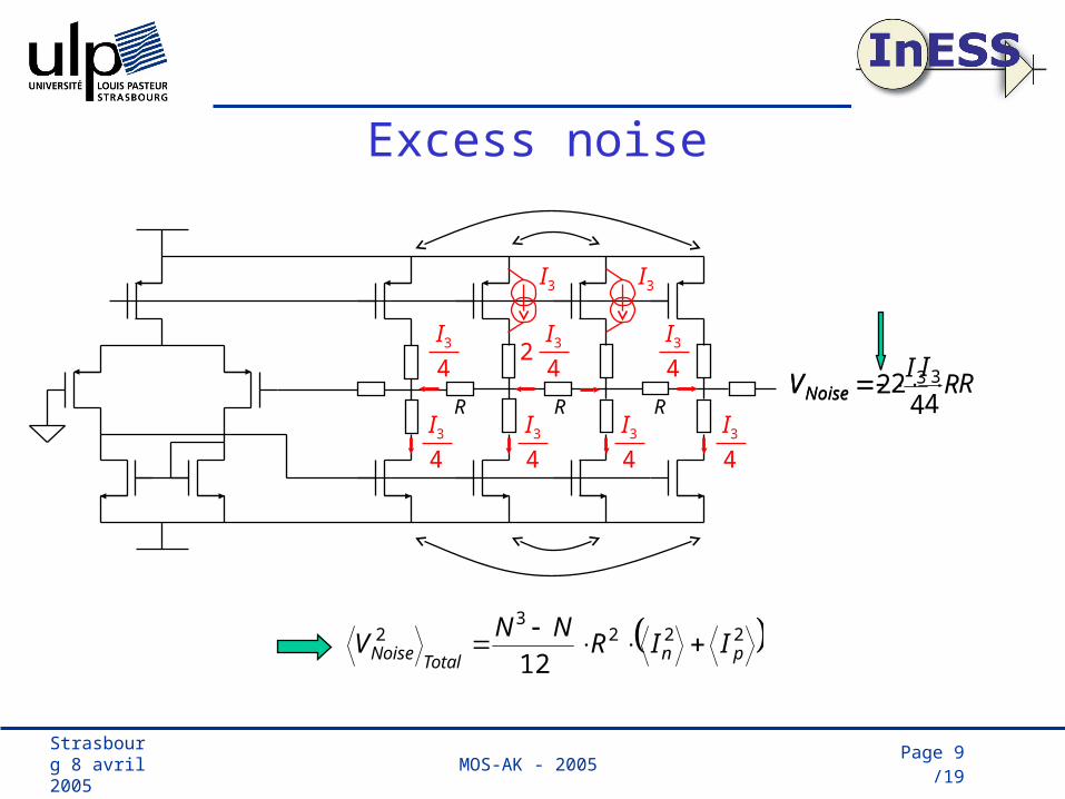
Excess noise
R R R
2223
2
12 pnTotalNoise IIRNN
V
RI
VNoise 4
2 3 RI
VNoise 4
2 3
I3
I3
4
I3
4
I3
4
I3
4
I3
4
I3
42
I3
4
I3
MOS-AK - 2005Page 10
/19Strasbourg 8 avril 2005
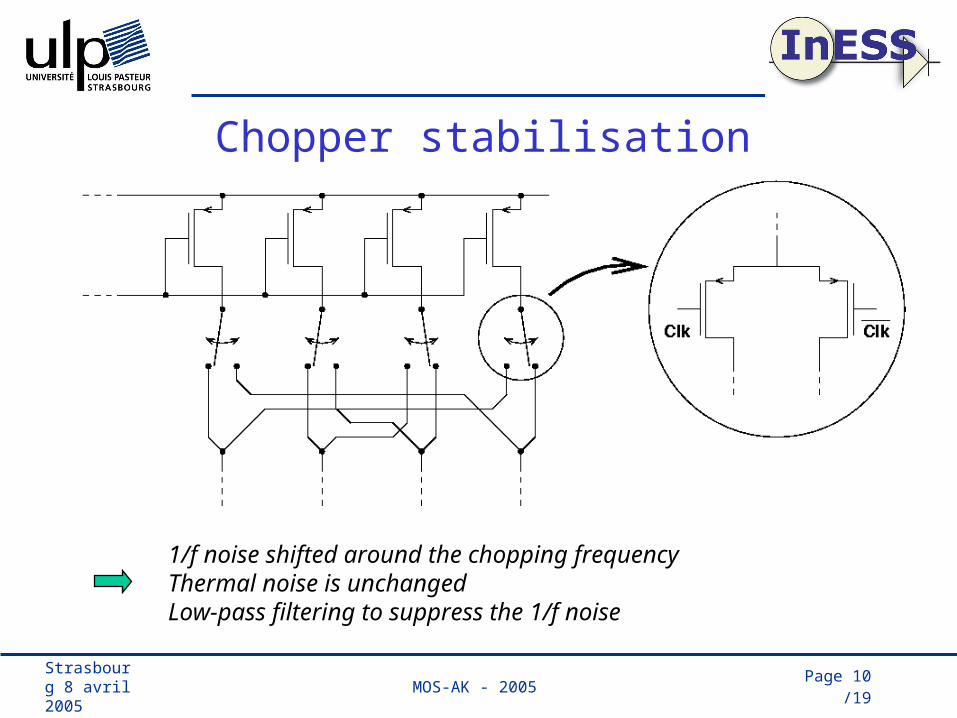
Chopper stabilisation
1/f noise shifted around the chopping frequencyThermal noise is unchangedLow-pass filtering to suppress the 1/f noise
MOS-AK - 2005Page 11
/19Strasbourg 8 avril 2005
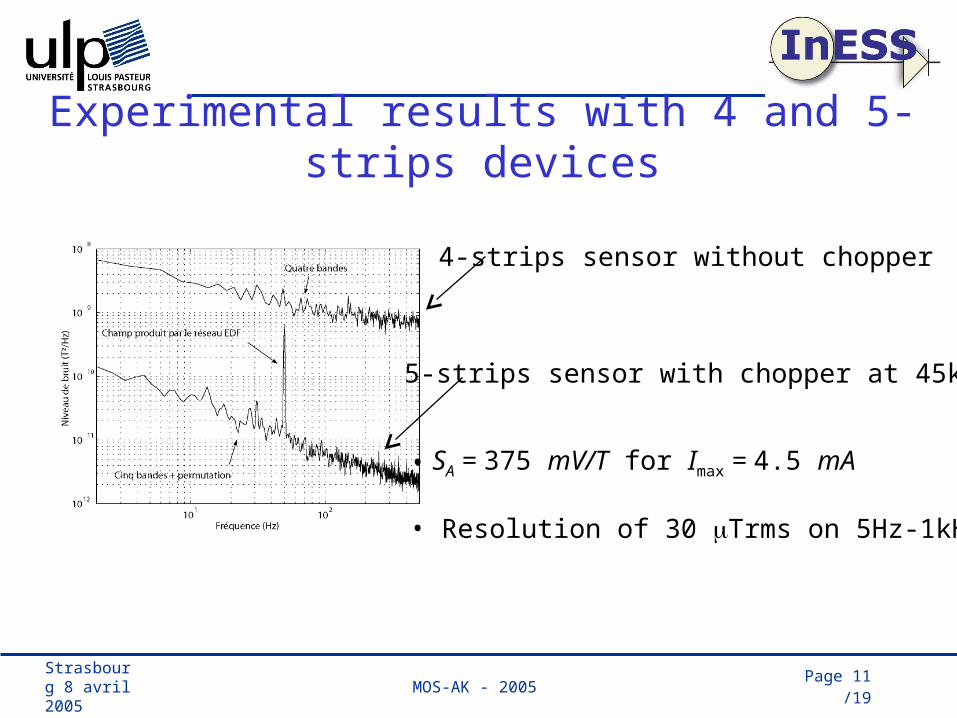
Experimental results with 4 and 5-strips devices
4-strips sensor without chopper
5-strips sensor with chopper at 45kHz
• SA = 375 mV/T for Imax = 4.5 mA
• Resolution of 30 Trms on 5Hz-1kHz
MOS-AK - 2005Page 12
/19Strasbourg 8 avril 2005
Need for accurate models
• Hall effect sensors are easy to integrate in CMOS
• Smart biasing and signal conditioning
• Noise level depends on the material properties and on the electrical
resistance R between adjacent strips
• Effective sensitivity depends on the ratio R/r where r is the output
resistance of the biasing transistors
• Non-linearity depends on the extension of the depleted zones
• Temperature,…
Accurate compact models are required for these sensorsto be widely used.
MOS-AK - 2005Page 13
/19Strasbourg 8 avril 2005
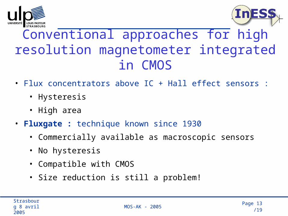
Conventional approaches for high resolution magnetometer integrated in CMOS
• Flux concentrators above IC + Hall effect sensors :
• Hysteresis
• High area
• Fluxgate : technique known since 1930
• Commercially available as macroscopic sensors
• No hysteresis
• Compatible with CMOS
• Size reduction is still a problem!
MOS-AK - 2005Page 14
/19Strasbourg 8 avril 2005
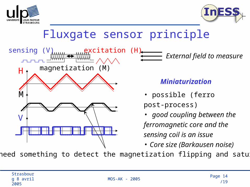
Fluxgate sensor principlesensing (V) excitation (H)
H magnetization (M)
M
V
External field to measure
Miniaturization
• possible (ferro post-
process)• good coupling between the
ferromagnetic core and the
sensing coil is an issue• Core size (Barkausen noise)
We need something to detect the magnetization flipping and saturation
MOS-AK - 2005Page 15
/19Strasbourg 8 avril 2005
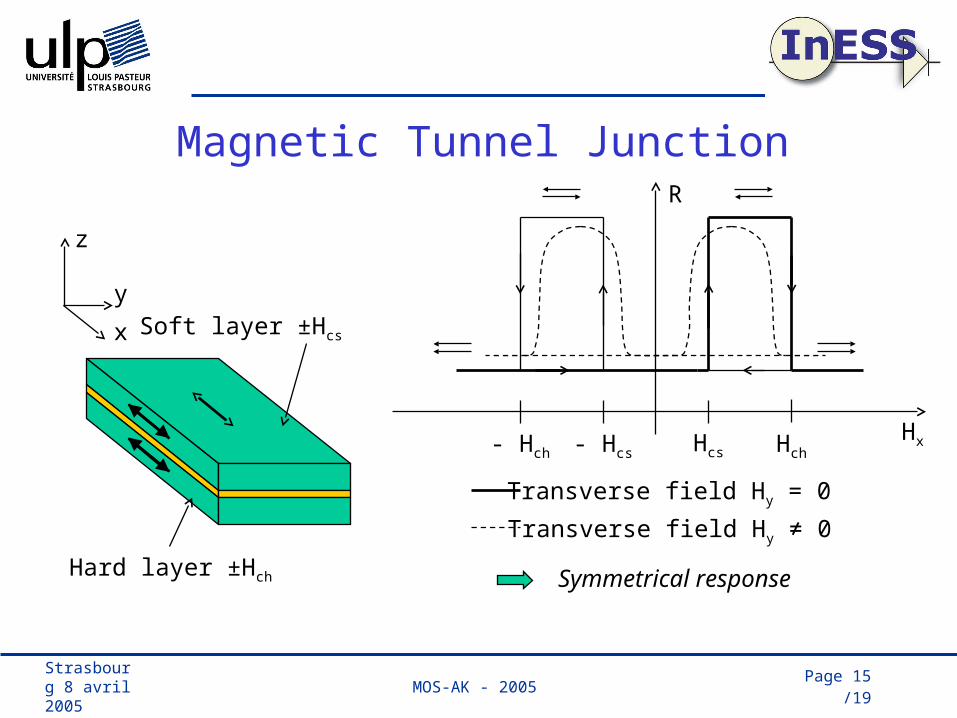
Magnetic Tunnel Junction
Soft layer ±Hcsx
y
z
Hard layer ±Hch
Hcs Hch- Hcs- HchHx
Transverse field Hy = 0
R
Transverse field Hy ≠ 0
Symmetrical response
MOS-AK - 2005Page 16
/19Strasbourg 8 avril 2005
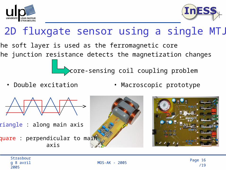
2D fluxgate sensor using a single MTJ• The soft layer is used as the ferromagnetic core• The junction resistance detects the magnetization changes
• Double excitation
no core-sensing coil coupling problem
• Macroscopic prototype
Triangle : along main axis
Square : perpendicular to main axis

MOS-AK - 2005Page 17
/19Strasbourg 8 avril 2005
Experimental results
Along the main axis :
1086 V/T
Perpendicular to main axis :
534 V/T
Resolution :
Integrated version
HzT /2
Resolution 1 nT
MOS-AK - 2005Page 18
/19Strasbourg 8 avril 2005
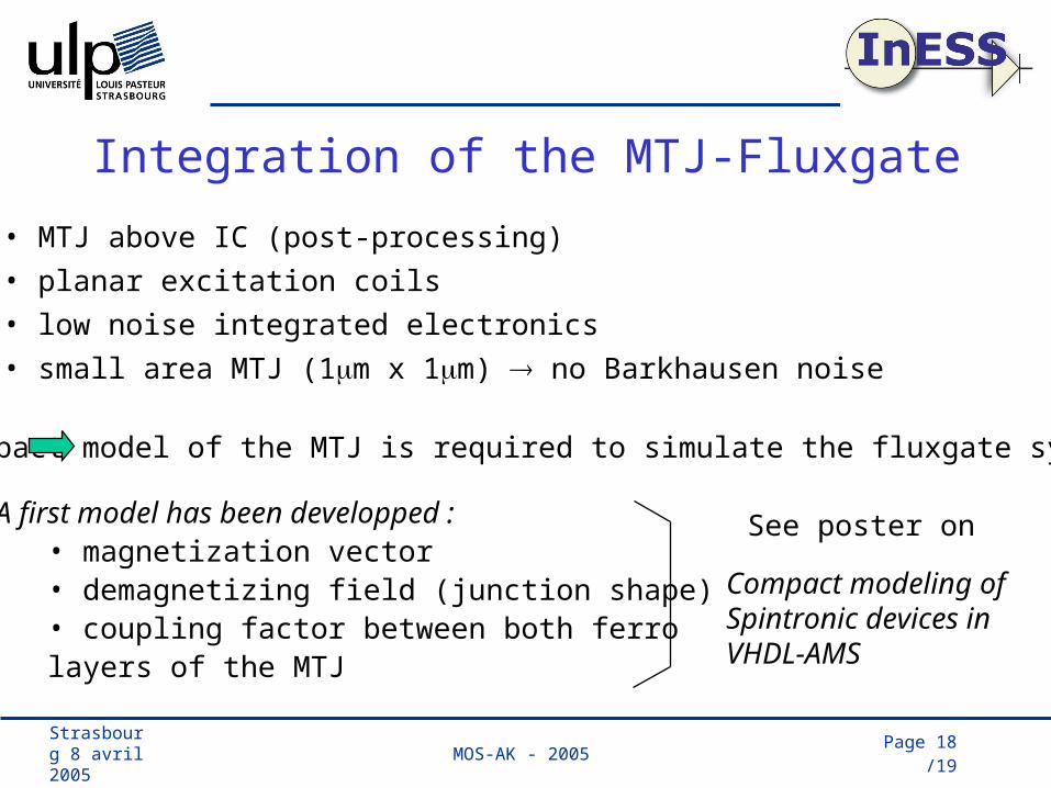
Integration of the MTJ-Fluxgate
• MTJ above IC (post-processing)
• planar excitation coils
• low noise integrated electronics
• small area MTJ (1m x 1m) no Barkhausen noise
Compact model of the MTJ is required to simulate the fluxgate system!
A first model has been developped :• magnetization vector• demagnetizing field (junction shape)• coupling factor between both ferrolayers of the MTJ
See poster on
Compact modeling ofSpintronic devices inVHDL-AMS
MOS-AK - 2005Page 19
/19Strasbourg 8 avril 2005
Conclusion
• Not only MOS transistors in CMOS chip
• Hall effect sensors can find wide applications
• Fully compatible with CMOS
• On-chip circuitry advantage
• Need for accurate compact models
• High resolution magnetometers
• Resolution below 1nT
• Post-process cost justified by high resolution
• Need for compact models for spintronic devices


![Bebevo BM201 User Manual · %hehn qlwhvl yh ndeorvxqx eheh÷lql]lq xodúdpd\dfd÷Õ elu phvdih\h \huohúwlulq %hehn yh hehyh\q qlwhohulql vÕyÕ whpdvÕqgdq qhpghq \ nvhn ÕvÕoÕ](https://img.pdfslide.net/doc/110x75/5ec1bda1ddef522ee3521166/bebevo-bm201-user-hehn-qlwhvl-yh-ndeorvxqx-ehehlqllq-xoddpddfd-elu-phvdihh.jpg)