Embed Size (px)
Citation preview

1
MOS Field-Effect Transistors
(MOSFETs)
ELZ 303 - Elektronik I
Dr. Mehmet Siraç Özerdem
Elektrik Elektronik Müh. Bölümü
Dicle Üniversitesi
Microelectronic Circuits – Fourth Edition
Adel S. Sedra, Kenneth C. Smith, 1998 Oxford University Press
Copyright 2004 by Oxford University Press, Inc.
Microelectronic Circuits - Fifth Edition Sedra/Smith
Physical structure of the enhancement-type NMOS transistor:
(a) perspective view;
(b) cross-section. Typically L = 0.1 to 3 mm, W = 0.2 to 100 mm,
and the thickness of the oxide layer (tox) is in the range of 2 to
50 nm.
The n-channel MOSFET

2
Copyright 2004 by Oxford University Press, Inc.
Microelectronic Circuits - Fifth Edition Sedra/Smith
Operation with no Gate Voltage
• Back-to-back diodes exist in series between D and S
• The path between D and S has a high resistance
Th
e n
-ch
an
ne
l MO
SF
ET
Microelectronic Circuits - Fifth Edition Sedra/Smith
Copyright 2004 by Oxford University Press, Inc.
Microelectronic Circuits - Fifth Edition Sedra/Smith
The enhancement-type NMOS transistor with VGS > 0
An n channel is induced at the top of the substrate beneath
the gate.
Th
e n
-ch
an
ne
l MO
SF
ET
When VGS > Vt (threshold voltage), channel is induced
1V < Vt < 3V
Creating a Channel

3
Copyright 2004 by Oxford University Press, Inc.
Microelectronic Circuits - Fifth Edition Sedra/Smith
Specifically, the channel conductance is proportional to vGS – Vt’ and
thus iD is proportional to (vGS – Vt) and vDS.
Th
e n
-ch
an
ne
l MO
SF
ET
Applying a small VDS
Copyright 2004 by Oxford University Press, Inc.
Microelectronic Circuits - Fifth Edition Sedra/Smith
The iD–vDS characteristics of the MOSFET
The device operates as a linear resistor controlled by vGS.
Th
e n
-ch
an
nel M
OS
FE
T

4
Copyright 2004 by Oxford University Press, Inc.
Microelectronic Circuits - Fifth Edition Sedra/Smith
7
The induced channel acquires a tapered shape, and its resistance
increases as vDS is increased.
Th
e n
-ch
an
ne
l MO
SF
ET
Operation as VDS is increased
Copyright 2004 by Oxford University Press, Inc.
Increasing vDS causes the channel to acquire a tapered shape.
Eventually, as vDS reaches vGS – Vt’ the channel is pinched off
at the drain end. Increasing vDS above vGS – Vt has little effect
(theoretically, no effect) on the channel’s shape. Microelectronic Circuits - Fifth Edition Sedra/Smith
The n-channel MOSFET

5
Copyright 2004 by Oxford University Press, Inc.
Microelectronic Circuits - Fifth Edition Sedra/Smith
iD versus vDS for an enhancement-type NMOS transistor
operated with vGS > Vt
The n-channel MOSFET
Copyright 2004 by Oxford University Press, Inc.
Microelectronic Circuits - Fifth Edition Sedra/Smith
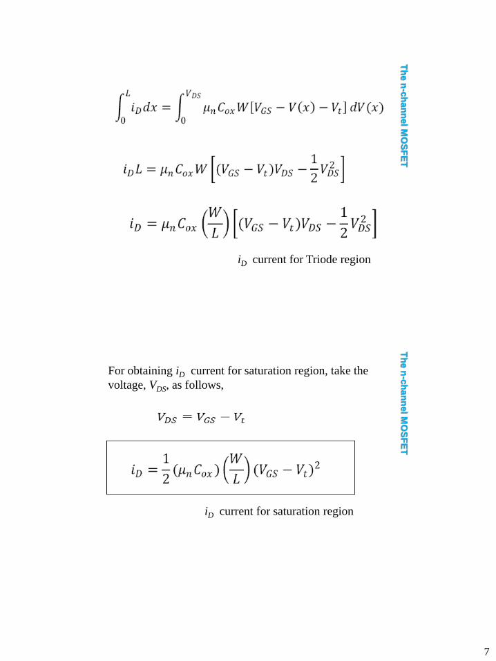
Derivation of the iD–vDS Relationship

6
Copyright 2004 by Oxford University Press, Inc.
Microelectronic Circuits - Fifth Edition Sedra/Smith
Th
e n
-ch
an
ne
l MO
SF
ET
Copyright 2004 by Oxford University Press, Inc.
Microelectronic Circuits - Fifth Edition Sedra/Smith
Th
e n
-ch
an
nel M
OS
FE
T
7
Copyright 2004 by Oxford University Press, Inc.
Microelectronic Circuits - Fifth Edition Sedra/Smith
iD current for Triode region
Th
e n
-ch
an
nel M
OS
FE
T
Copyright 2004 by Oxford University Press, Inc.
Microelectronic Circuits - Fifth Edition Sedra/Smith
For obtaining iD current for saturation region, take the
voltage, VDS, as follows,
iD current for saturation region
Th
e n
-ch
an
nel M
OS
FE
T
8
Copyright 2004 by Oxford University Press, Inc.
Microelectronic Circuits - Fifth Edition Sedra/Smith
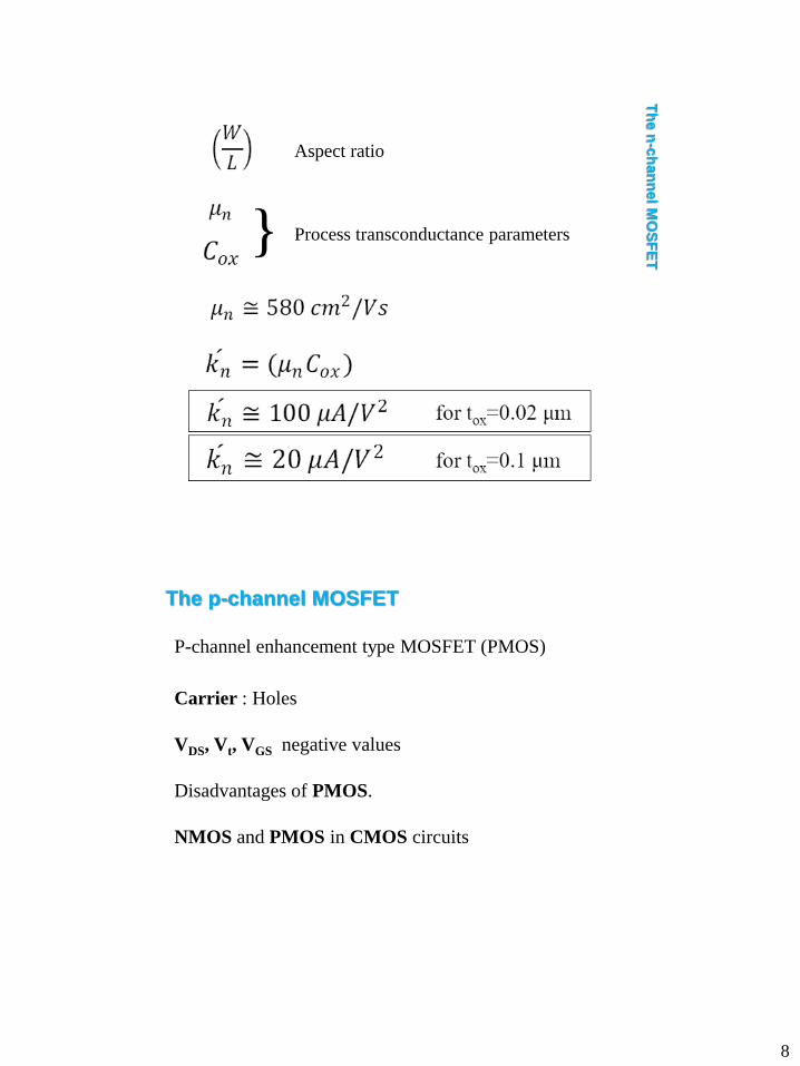
Aspect ratio
} Process transconductance parameters
Th
e n
-ch
an
nel M
OS
FE
T
Copyright 2004 by Oxford University Press, Inc.
Microelectronic Circuits - Fifth Edition Sedra/Smith
P-channel enhancement type MOSFET (PMOS)
The p-channel MOSFET
Carrier : Holes
VDS, Vt, VGS negative values
Disadvantages of PMOS.
NMOS and PMOS in CMOS circuits

9
Copyright 2004 by Oxford University Press, Inc. Microelectronic Circuits - Fifth Edition Sedra/Smith
Note that the PMOS transistor is formed in a separate n-type
region, known as an n well. Another arrangement is also
possible in which an n-type body is used and the n device is
formed in a p well.
Complementary MOS (CMOS)
Copyright 2004 by Oxford University Press, Inc.
Microelectronic Circuits - Fifth Edition Sedra/Smith
(a) Circuit symbol for the NMOS.
(b) Modified circuit symbol with an arrowhead on the source
terminal to distinguish it from the drain and to indicate device
polarity (i.e., n channel).
(c) Simplified circuit symbol to be used when the source is
connected to the body or when the effect of the body on device
operation is unimportant.
The n-channel MOSFET
10
Copyright 2004 by Oxford University Press, Inc.
Microelectronic Circuits - Fifth Edition Sedra/Smith
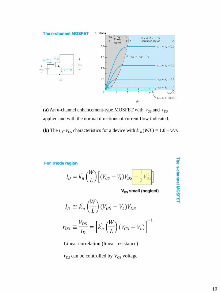
(a) An n-channel enhancement-type MOSFET with vGS and vDS
applied and with the normal directions of current flow indicated.
(b) The iD–vDS characteristics for a device with k’n (W/L) = 1.0 mA/V2.
The n-channel MOSFET
Copyright 2004 by Oxford University Press, Inc.
Microelectronic Circuits - Fifth Edition Sedra/Smith
For Triode region
Linear correlation (linear resistance)
rDS can be controlled by VGS voltage
Th
e n
-ch
an
ne
l MO
SF
ET

11
Copyright 2004 by Oxford University Press, Inc.
Microelectronic Circuits - Fifth Edition Sedra/Smith
The iD–vGS characteristic for an enhancement-type NMOS
transistor in saturation
For saturation region
Vt = 1 V
k’n (W/L) =1.0 mA/V2
Th
e n
-ch
an
ne
l MO
SF
ET
Copyright 2004 by Oxford University Press, Inc.
Large-signal equivalent-circuit model of an n-channel
MOSFET operating in the saturation region.
Microelectronic Circuits - Fifth Edition Sedra/Smith The n-channel MOSFET
Ideal model

12
Copyright 2004 by Oxford University Press, Inc.
For the broken line characteristic
Microelectronic Circuits - Fifth Edition Sedra/Smith
vGS - Vt = vDS
substitute it in the either triode region equation or
the saturation region equation.
Copyright 2004 by Oxford University Press, Inc.
The relative levels of the terminal voltages of the enhancement
NMOS transistor for operation in the triode region and in the
saturation region.
Microelectronic Circuits - Fifth Edition Sedra/Smith The n-channel MOSFET

13
Copyright 2004 by Oxford University Press, Inc.
Increasing vDS beyond vDSsat causes the channel pinch-off
point to move slightly away from the drain, thus reducing the effective channel length (by ΔL).
Microelectronic Circuits - Fifth Edition Sedra/Smith 0.03 > λ > 0.005
Th
e n
-ch
an
nel
MO
SF
ET
Copyright 2004 by Oxford University Press, Inc.
Effect of vDS on iD in the saturation region. The MOSFET
parameter VA depends on the process technology and, for a
given process, is proportional to the channel length L.
Microelectronic Circuits - Fifth Edition Sedra/Smith
200V > VA > 30V
The n-channel MOSFET

14
Copyright 2004 by Oxford University Press, Inc.
Microelectronic Circuits - Fifth Edition Sedra/Smith
The n-channel MOSFET
Copyright 2004 by Oxford University Press, Inc. 28
Large-signal equivalent circuit model of the n-channel
MOSFET in saturation, incorporating the output resistance ro.
Microelectronic Circuits - Fifth Edition Sedra/Smith The n-channel MOSFET

15
Copyright 2004 by Oxford University Press, Inc. 29
(a) Circuit symbol of PMOS
(b) Modified symbol with an
arrowhead on the source lead
(c) Simplified circuit symbol
for the case where the source
is connected to the body
(d) The MOSFET with
voltages applied and the
directions of current flow
indicated. Note that iD flows
out of the drain terminal.
Microelectronic Circuits - Fifth Edition Sedra/Smith
Characteristics of the p-channel MOSFET
The p-channel MOSFET
Copyright 2004 by Oxford University Press, Inc. 30
Microelectronic Circuits - Fifth Edition Sedra/Smith
Characteristics of the p-channel MOSFET
VGS ,VDS ,Vt and λ are all negative.

16
Copyright 2004 by Oxford University Press, Inc. 31
The relative levels of the terminal voltages of the
enhancement-type PMOS transistor for operation in
the triode region and in the saturation region.
Microelectronic Circuits - Fifth Edition Sedra/Smith
Characteristics of the p-channel MOSFET
The p-channel MOSFET
Copyright 2004 by Oxford University Press, Inc. 32
Microelectronic Circuits - Fifth Edition Sedra/Smith
The p-channel MOSFET
The n-channel MOSFET
17
Copyright 2004 by Oxford University Press, Inc.
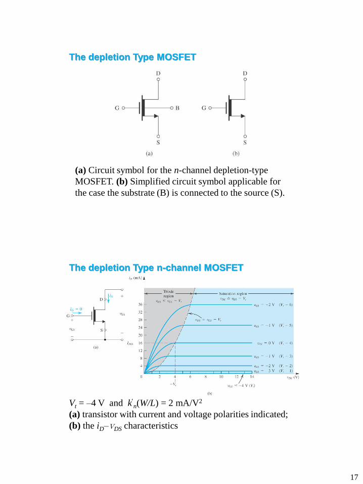
(a) Circuit symbol for the n-channel depletion-type
MOSFET. (b) Simplified circuit symbol applicable for
the case the substrate (B) is connected to the source (S).
The depletion Type MOSFET
Microelectronic Circuits - Fifth Edition Sedra/Smith
Copyright 2004 by Oxford University Press, Inc.
Microelectronic Circuits - Fifth Edition Sedra/Smith
The depletion Type n-channel MOSFET
Vt = –4 V and kn(W/L) = 2 mA/V2
(a) transistor with current and voltage polarities indicated;
(b) the iD–vDS characteristics

18
Copyright 2004 by Oxford University Press, Inc.
Microelectronic Circuits - Fifth Edition Sedra/Smith
The iD–vGS characteristic in saturation.
The depletion Type n-channel MOSFET
Copyright 2004 by Oxford University Press, Inc.
The relative levels of terminal voltages of a depletion-
type NMOS transistor for operation in the triode and the
saturation regions. The case shown is for operation in
the enhancement mode (vGS is positive).
The depletion Type n-channel MOSFET
Microelectronic Circuits - Fifth Edition Sedra/Smith

19
Copyright 2004 by Oxford University Press, Inc.
Microelectronic Circuits - Fifth Edition Sedra/Smith
Sketches of the iD–vGS characteristics for MOSFETs of
enhancement and depletion types, of both polarities (operating
in saturation). Note that the characteristic curves intersect the
vGS axis at Vt. Also note that for generality somewhat different
values of |Vt| are shown for n-channel and p-channel devices.
The depletion Type MOSFET
Copyright 2004 by Oxford University Press, Inc.
Microelectronic Circuits - Fifth Edition Sedra/Smith
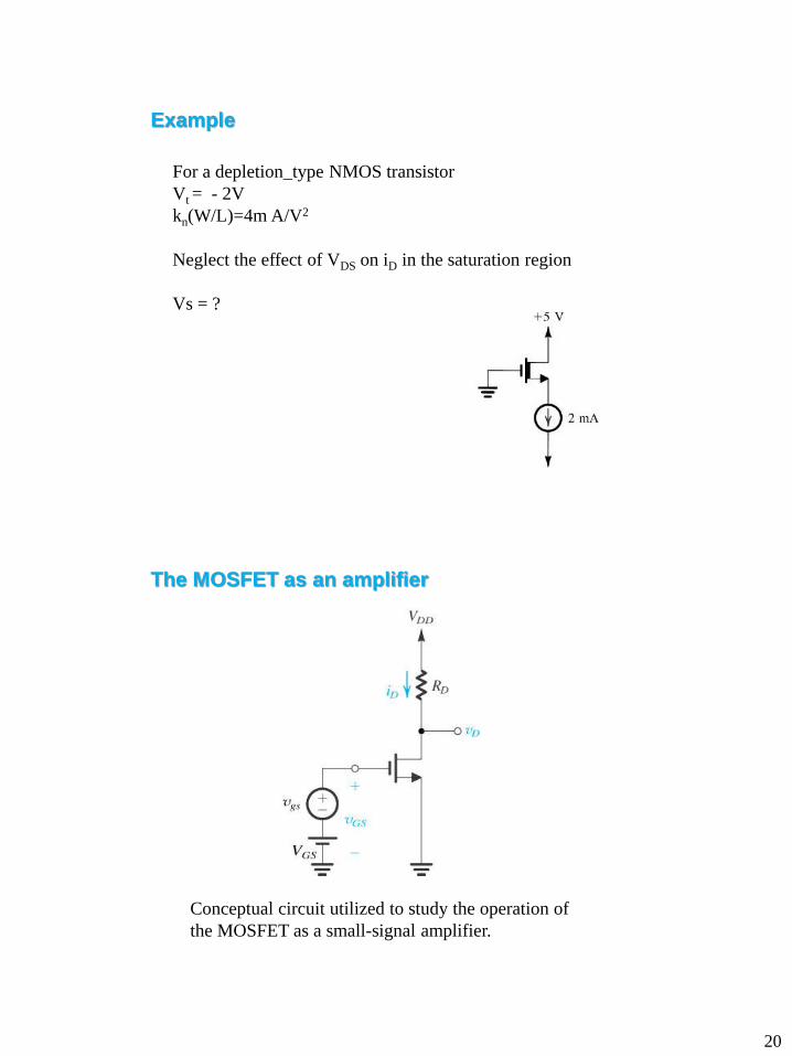
Example
For a depletion_type NMOS transistor
Vt = - 2V
kn(W/L)=2m A/V2
a) Find the minimum VDS required to operate in the
saturation region, when VGS=1V
b) iD=?
20
Copyright 2004 by Oxford University Press, Inc.
Microelectronic Circuits - Fifth Edition Sedra/Smith
Example
For a depletion_type NMOS transistor
Vt = - 2V
kn(W/L)=4m A/V2
Neglect the effect of VDS on iD in the saturation region
Vs = ?
Copyright 2004 by Oxford University Press, Inc.
Microelectronic Circuits - Fifth Edition Sedra/Smith
The MOSFET as an amplifier
Conceptual circuit utilized to study the operation of
the MOSFET as a small-signal amplifier.

21
Copyright 2004 by Oxford University Press, Inc.
Microelectronic Circuits - Fifth Edition Sedra/Smith
The MOSFET as an amplifier
To find the dc bias or operating point of the MOSFET,
we set the signal vgs = 0 (assume that λ=0).
Copyright 2004 by Oxford University Press, Inc.
Microelectronic Circuits - Fifth Edition Sedra/Smith
The MOSFET as an amplifier
vgs ≠ 0 (assume that λ=0).

22
Copyright 2004 by Oxford University Press, Inc. 43
Small-signal operation of the enhancement MOSFET amplifier
Microelectronic Circuits - Fifth Edition Sedra/Smith
Copyright 2004 by Oxford University Press, Inc. 44
Voltage Gain
Microelectronic Circuits - Fifth Edition Sedra/Smith

23
Copyright 2004 by Oxford University Press, Inc. 45
Total instantaneous
voltages vGS and vD
for the circuit. Microelectronic Circuits - Fifth Edition Sedra/Smith
Copyright 2004 by Oxford University Press, Inc.
Microelectronic Circuits - Fifth Edition Sedra/Smith
(a) neglecting the dependence of iD on vDS in saturation (the
channel-length modulation effect);
(b) including the effect of channel-length modulation,
modeled by output resistance ro = |VA| /ID.
Small-signal equivalent circuit models
24
Copyright 2004 by Oxford University Press, Inc.
Microelectronic Circuits - Fifth Edition Sedra/Smith
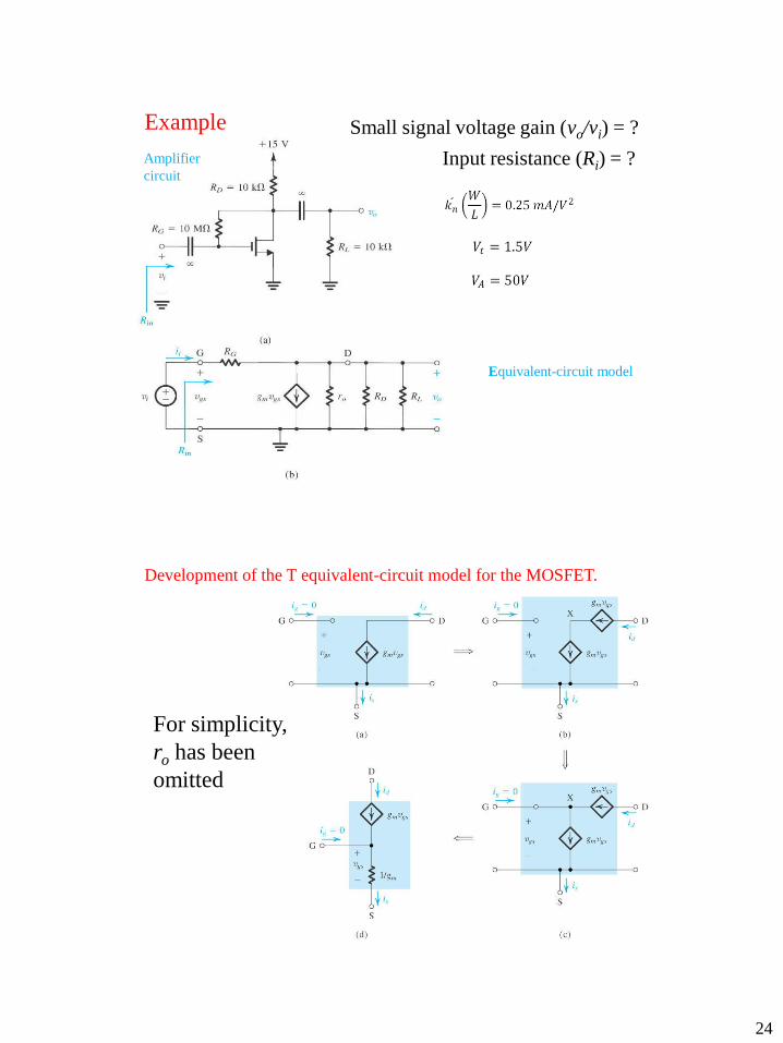
Equivalent-circuit model
Example Small signal voltage gain (vo/vi) = ?
Input resistance (Ri) = ? Amplifier
circuit
Copyright 2004 by Oxford University Press, Inc. Microelectronic Circuits - Fifth Edition Sedra/Smith
For simplicity,
ro has been
omitted
Development of the T equivalent-circuit model for the MOSFET.

25
Copyright 2004 by Oxford University Press, Inc. Microelectronic Circuits - Fifth Edition Sedra/Smith
ro can be added between D and S in the T model
Development of the T equivalent-circuit model for the MOSFET.
Copyright 2004 by Oxford University Press, Inc. Microelectronic Circuits - Fifth Edition Sedra/Smith
Biasing in MOS Amplifier Circuits

26
Copyright 2004 by Oxford University Press, Inc. Microelectronic Circuits - Fifth Edition Sedra/Smith
The High_Frequency MOSFET Model
Copyright 2004 by Oxford University Press, Inc. Microelectronic Circuits - Fifth Edition Sedra/Smith
The High_Frequency MOSFET Model
27
Copyright 2004 by Oxford University Press, Inc. Microelectronic Circuits - Fifth Edition Sedra/Smith
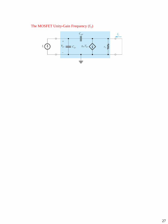
The MOSFET Unity-Gain Frequency (fT)