Embed Size (px)
Citation preview
© 1995
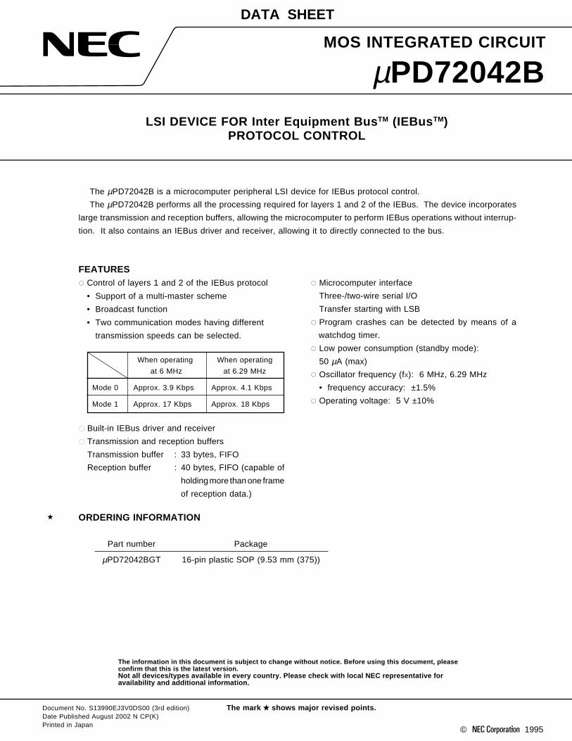
DATA SHEET
LSI DEVICE FOR Inter Equipment BusTM (IEBusTM)PROTOCOL CONTROL
MOS INTEGRATED CIRCUIT
µPD72042B
The µPD72042B is a microcomputer peripheral LSI device for IEBus protocol control.
The µPD72042B performs all the processing required for layers 1 and 2 of the IEBus. The device incorporates
large transmission and reception buffers, allowing the microcomputer to perform IEBus operations without interrup-
tion. It also contains an IEBus driver and receiver, allowing it to directly connected to the bus.
FEATURES
•• Control of layers 1 and 2 of the IEBus protocol
• Support of a multi-master scheme
• Broadcast function
• Two communication modes having different
transmission speeds can be selected.
•• Microcomputer interface
Three-/two-wire serial I/O
Transfer starting with LSB
•• Program crashes can be detected by means of a
watchdog timer.
•• Low power consumption (standby mode):
50 µA (max)
•• Oscillator frequency (fX): 6 MHz, 6.29 MHz
• frequency accuracy: ±1.5%
•• Operating voltage: 5 V ±10%
When operating When operating
at 6 MHz at 6.29 MHz
Mode 0 Approx. 3.9 Kbps Approx. 4.1 Kbps
Mode 1 Approx. 17 Kbps Approx. 18 Kbps
Built-in IEBus driver and receiver
Transmission and reception buffers
Transmission buffer : 33 bytes, FIFO
Reception buffer : 40 bytes, FIFO (capable of
holding more than one frame
of reception data.)
ORDERING INFORMATION
Part number Package
µPD72042BGT 16-pin plastic SOP (9.53 mm (375))
The mark shows major revised points.Document No. S13990EJ3V0DS00 (3rd edition)Date Published August 2002 N CP(K)Printed in Japan
The information in this document is subject to change without notice. Before using this document, pleaseconfirm that this is the latest version.Not all devices/types available in every country. Please check with local NEC representative foravailability and additional information.
µPD72042B
2 Data Sheet S13990EJ3V0DS
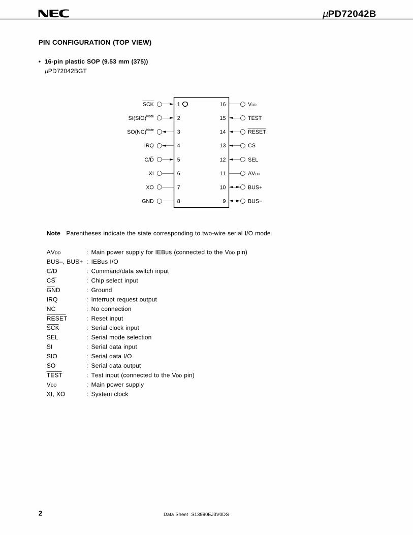
PIN CONFIGURATION (TOP VIEW)
• 16-pin plastic SOP (9.53 mm (375))
µPD72042BGT
1
2
3
4
5
6
7
8
VDD
TEST
RESET
CS
SEL
AVDD
BUS+
BUS−
16
15
14
13
12
11
10
9
SCK
SI(SIO)Note
SO(NC)Note
IRQ
C/D
XI
XO
GND
Note Parentheses indicate the state corresponding to two-wire serial I/O mode.
AVDD : Main power supply for IEBus (connected to the VDD pin)
BUS–, BUS+ : IEBus I/O
C/D : Command/data switch input
CS : Chip select input
GND : Ground
IRQ : Interrupt request output
NC : No connection
RESET : Reset input
SCK : Serial clock input
SEL : Serial mode selection
SI : Serial data input
SIO : Serial data I/O
SO : Serial data output
TEST : Test input (connected to the VDD pin)
VDD : Main power supply
XI, XO : System clock
µPD72042B
3Data Sheet S13990EJ3V0DS
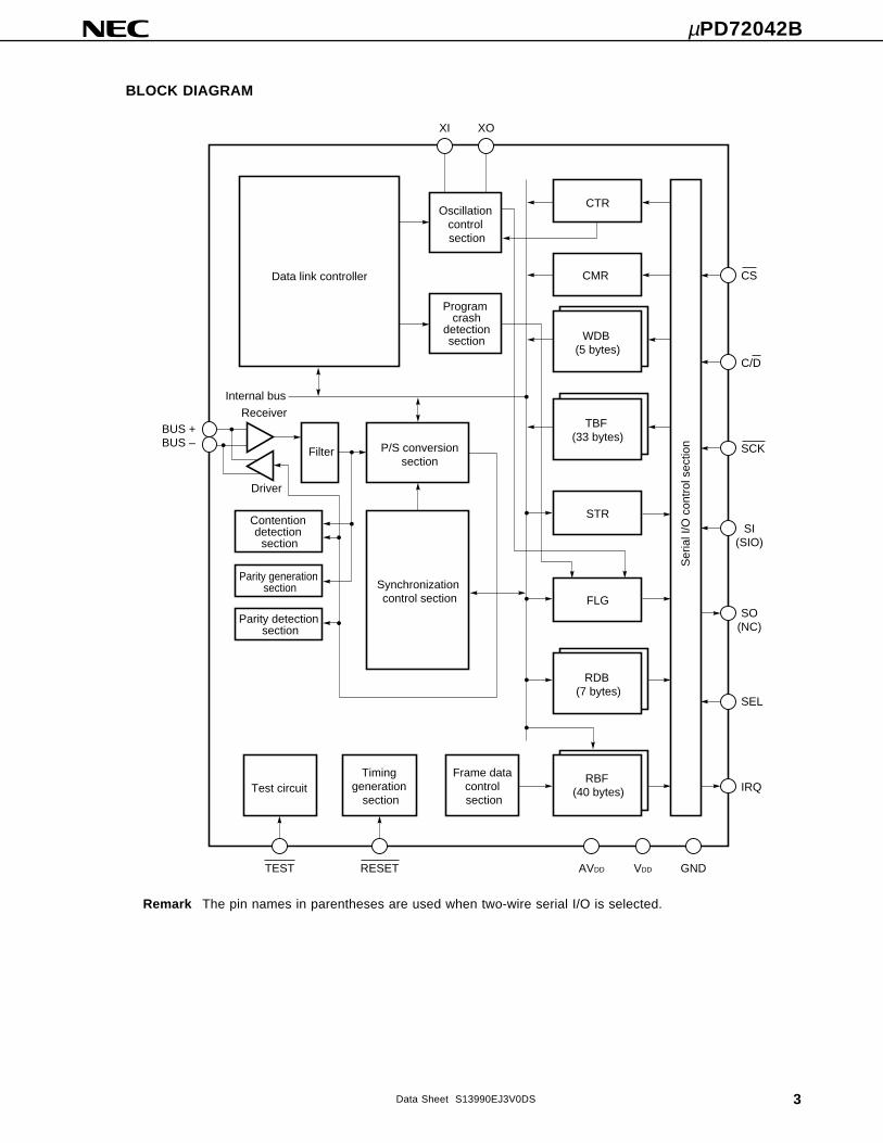
BLOCK DIAGRAM
BUS +BUS –
XI XO
CTR
CMR
TBF (33 bytes)
STR
FLG
RBF (40 bytes)
TEST RESET AVDD VDD GND
IRQ
SEL
SO(NC)
SI(SIO)
SCK
C/D
CSData link controller
Oscillation control section
Program crash
detectionsection
Internal bus
Receiver
Driver
Filter P/S conversionsection
Ser
ial I
/O c
ontr
ol s
ectio
n
Contention detection
section
Parity generation section
Parity detection section
Synchronization control section
Test circuitTiming
generation section
Frame data control section
RDB (7 bytes)
WDB (5 bytes)
Remark The pin names in parentheses are used when two-wire serial I/O is selected.
µPD72042B
4 Data Sheet S13990EJ3V0DS
CONTENTS
1. PIN FUNCTIONS ............................................................................................................................. 61.1 PIN FUNCTIONS..................................................................................................................................... 6
2. IEBus OPERATION......................................................................................................................... 82.1 OVERVIEW .............................................................................................................................................. 8
2.2 IEBus COMMUNICATION PROTOCOL ................................................................................................ 9
2.2.1 Bus Mastership Determination (Arbitration) ............................................................................... 10
2.2.2 Communication Mode ................................................................................................................. 10
2.2.3 Communication Address ............................................................................................................. 11
2.2.4 Broadcast ..................................................................................................................................... 11
2.3 TRANSMISSION PROTOCOL ............................................................................................................... 11
2.4 TRANSMISSION DATA (CONTENTS OF THE DATA FIELD) ............................................................. 17
2.5 BIT FORMAT ........................................................................................................................................... 21
3. MICROCOMPUTER INTERFACE .................................................................................................. 223.1 TRANSFER METHOD ............................................................................................................................ 22
3.2 DATA TRANSFER FORMAT .................................................................................................................. 23
3.2.1 Three-Wire Data Transfer (SEL = 1) .......................................................................................... 23
3.2.2 Two-Wire Data Transfer (SEL = 0) ............................................................................................. 25
3.3 CONNECTION TO A MICROCOMPUTER............................................................................................. 27
3.4 STANDBY MODE SETTING AND CANCELLATION ............................................................................ 28
3.5 RESET MODE SETTING AND CANCELLATION ................................................................................. 28
4. REGISTERS .................................................................................................................................... 29
5. EXAMPLE TIMINGS FOR COMMUNICATION.............................................................................. 59
6. EXAMPLE MICROCOMPUTER PROCESSING FLOW ................................................................ 676.1 COMMUNICATION FLAGS .................................................................................................................... 68
6.2 MAIN ROUTINE ...................................................................................................................................... 69
6.3 INTERRUPT ROUTINE ........................................................................................................................... 70
6.4 PROCESSING ROUTINES ..................................................................................................................... 72
6.4.1 µPD72042B Initial Setting Routine ............................................................................................. 72
6.4.2 Communication Flag Initialization Routine ................................................................................. 72
6.4.3 Command Processing Routine ................................................................................................... 73
6.4.4 Master Communication Processing Routine .............................................................................. 73
6.4.5 Slave Data Transmission Processing Routine ........................................................................... 77
6.4.6 Transmission Processing Routine .............................................................................................. 80
6.4.7 Reception Processing Routine ................................................................................................... 81
7. ELECTRICAL CHARACTERISTICS .............................................................................................. 82
8. PACKAGE DRAWING ..................................................................................................................... 86
µPD72042B
5Data Sheet S13990EJ3V0DS
9. RECOMMENDED SOLDERING CONDITIONS ............................................................................. 87
APPENDIX A MAIN DIFFERENCES BETWEEN µµµµµPD72042A, µµµµµPD72042B, AND µµµµµPD6708 ......... 88
APPENDIX B IEBus PROTOCOL ANALYZER .................................................................................. 88

µPD72042B
6 Data Sheet S13990EJ3V0DS
1. PIN FUNCTIONS
1.1 PIN FUNCTIONS
Pin No.
1
2
3
4
5
6
7
8
9
10
11
12
13
PinNote
SCK
SI (SIO)
SO (NC)
IRQ
C/D
XI
XO
GND
BUS–
BUS+
AVDD
SEL
CS
I/ONote
Input
Input (I/O)
Output
(none)
Output
Input
–
–
I/O
–
Input
Input
Function
Serial clock input pin for CPU interface
Serial data pin for CPU interface. (This pin
functions as an input pin when 3-wire serial
I/O mode is selected, or as an I/O pin when
2-wire serial I/O mode is selected.)
Serial data output pin for CPU interface. (The
pin functions as an output when 3-wire serial I/O
mode is selected. When 2-wire serial I/O mode
is selected, the pin is left open.)
Output pin for making an interrupt request to the
CPU. When a return code or a program crash is
detected, a high-level signal is output on this pin
for at least 8 µs.
Input pin used to select control mode or data
read/write mode. When this pin is driven high,
internal register address setting and data read/
write are enabled. When the mode changes, the
serial clock counter is reset.
Pins for connecting a system clock resonator. A
6- or 6.29-MHz crystal or ceramic resonator
must be used. The accuracy of the frequency is
as follows;
Mode 0, 1: ±1.5%
Ground pin
I/O pins connected to the IEBus bus
Main power supply pin for the IEBus bus driver/
receiver. When used, this pin must be tied to
VDD.
Input pin used to select either 3- or 2-wire serial
I/O mode. A high-level signal on this pin selects
3-wire serial I/O mode. A low-level signal on this
pin selects 2-wire serial I/O mode.
Chip select pin. When this pin is driven low, the
serial interface is enabled. When this pin is
driven high, the SO pin becomes high-imped-
ance, and the serial clock counter is reset.
When reset[for both hardware
and software]
Input
Input
High-impedance
Low level
Input
When reset by
hardware (Oscil-
lation stopped)
XI = GND
XO = High level
When reset by
software (Oscil-
lation continued)
–
High-impedance
–
Input
Input
I/O formatNote
CMOS input
CMOS input
(CMOS I/O)
CMOS output
(none)
CMOS output
CMOS input
–
–
–
–
CMOS input
CMOS input
Note Parentheses indicate the state corresponding to two-wire serial I/O mode.
µPD72042B
7Data Sheet S13990EJ3V0DS
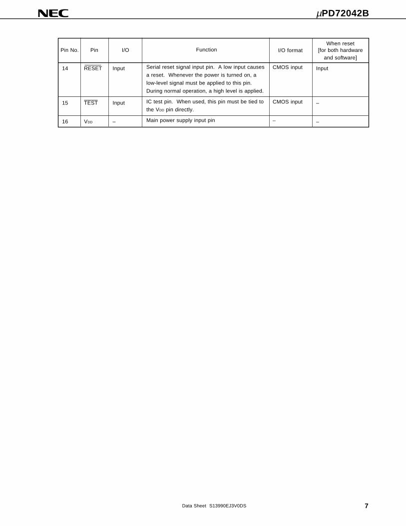
Pin No.
14
15
16
Pin
RESET
TEST
VDD
I/O
Input
Input
–
Function
Serial reset signal input pin. A low input causes
a reset. Whenever the power is turned on, a
low-level signal must be applied to this pin.
During normal operation, a high level is applied.
IC test pin. When used, this pin must be tied to
the VDD pin directly.
Main power supply input pin
When reset[for both hardware
and software]
Input
–
–
I/O format
CMOS input
CMOS input
–
µPD72042B
8 Data Sheet S13990EJ3V0DS
2. IEBus OPERATION
2.1 OVERVIEW
The µPD72042B is a CMOS LSI device for the IEBus interface.
The IEBus is designed to enable the data transmission between devices in a small-scale digital data transmission
system.
The µPD72042B is connected to a microcomputer built into a device. A serial interface (SCK, SO, and SI pins)
is used for connection. The host controller (microcomputer) sets the commands and data needed for data transmission
via this serial interface.
When data is transmitted, the host controller sets the data in the µPD72042B via the serial interface. Then, signals
are output on the BUS pins (BUS+, BUS–). When data is received from the BUS pins, the host controller can read
it via the serial interface.
µPD72042B
9Data Sheet S13990EJ3V0DS
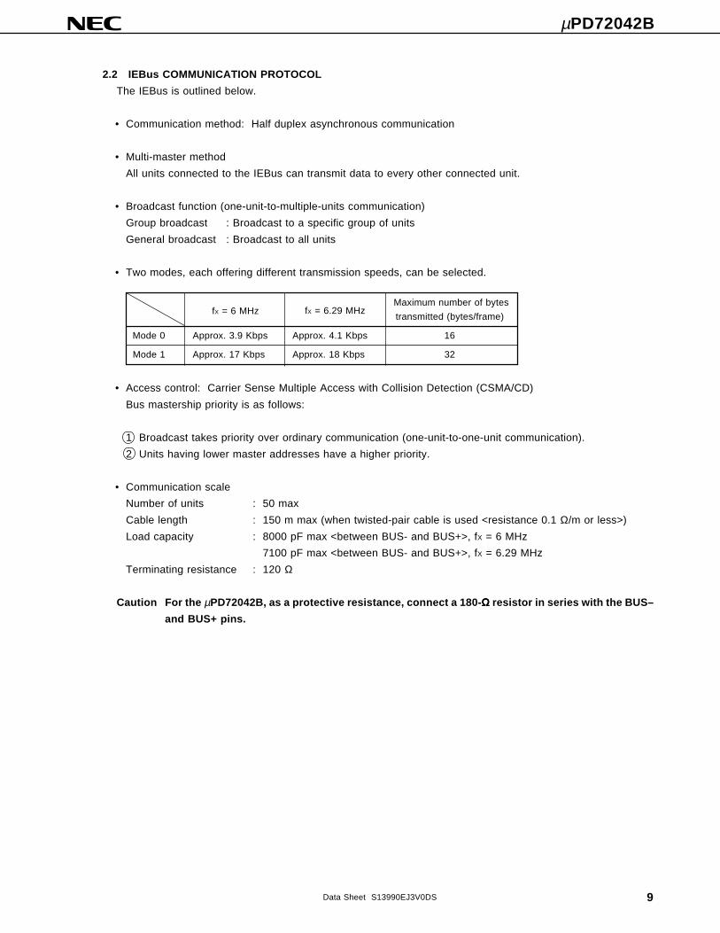
2.2 IEBus COMMUNICATION PROTOCOL
The IEBus is outlined below.
• Communication method: Half duplex asynchronous communication
• Multi-master method
All units connected to the IEBus can transmit data to every other connected unit.
• Broadcast function (one-unit-to-multiple-units communication)
Group broadcast : Broadcast to a specific group of units
General broadcast : Broadcast to all units
• Two modes, each offering different transmission speeds, can be selected.
Maximum number of bytes
transmitted (bytes/frame)
Mode 0 Approx. 3.9 Kbps Approx. 4.1 Kbps 16
Mode 1 Approx. 17 Kbps Approx. 18 Kbps 32
fX = 6 MHz fX = 6.29 MHz
• Access control: Carrier Sense Multiple Access with Collision Detection (CSMA/CD)
Bus mastership priority is as follows:
1 Broadcast takes priority over ordinary communication (one-unit-to-one-unit communication).
2 Units having lower master addresses have a higher priority.
• Communication scale
Number of units : 50 max
Cable length : 150 m max (when twisted-pair cable is used <resistance 0.1 Ω/m or less>)
Load capacity : 8000 pF max <between BUS- and BUS+>, fX = 6 MHz
7100 pF max <between BUS- and BUS+>, fX = 6.29 MHz
Terminating resistance : 120 Ω
Caution For the µPD72042B, as a protective resistance, connect a 180-ΩΩΩΩΩ resistor in series with the BUS–
and BUS+ pins.

µPD72042B
10 Data Sheet S13990EJ3V0DS
2.2.1 Bus Mastership Determination (Arbitration)
Before devices connected to the IEBus can control other devices, they must first acquire the bus. This operation
is called arbitration.
When more than one unit starts transmission at the same time, arbitration determines which of those units is allowed
to use the bus.
When arbitration results in only one device being granted bus mastership, the following bus mastership priority
conditions are used:
Remark Those devices that are defeated in arbitration can automatically enter retransmission mode. (For the
µPD72042B, the number of retransmissions can be set by specifying a value between 0 and 7 in the
MCR register.)
(1) Priority by communication type
Broadcast (one-unit-to-multiple-units communication) takes priority over ordinary communication (one-unit-to-
one-unit communication).
(2) Priority by master address
If the communication type is the same, the smallest master address value has the highest priority.
Example Each master address consists of 12 bits. A unit having master address 000H has the highest priority,
while a unit having master address FFFH has the lowest priority.
2.2.2 Communication Mode
The IEBus supports two communication modes, each having a different transmission speed. Table 2-1 lists the
transmission speed for each communication mode and the maximum number of bytes transmitted within one
communication frame.
Table 2-1 Transmission Speed and Maximum Number of Transmission
Bytes in Each Communication Mode
Communication modeMaximum number of transmission Effective transmission speedNote 1 (Kbps)
bytes (bytes/frame) fX = 6 MHzNote 2 fX = 6.29 MHzNote 2
0 16 Approx. 3.9 Approx. 4.1
1 32 Approx. 17 Approx. 18
Notes 1. Effective transmission speed at which the maximum transfer rate is achieved
2. Oscillator frequencies for the µPD72042B
Cautions 1. Before devices connected to the IEBus can perform communication, an appropriate commu-
nication mode must be set. Note that if a master unit and an associated unit (slave unit) have
different communication modes, they will not be able to communicate properly.
2. Communication cannot be performed properly between a unit operating at an oscillator
frequency of 6 MHz and another operating at 6.29 MHz, even when set to the same communication
mode. Units must use the same oscillator frequency to be able to communicate.
µPD72042B
11Data Sheet S13990EJ3V0DS
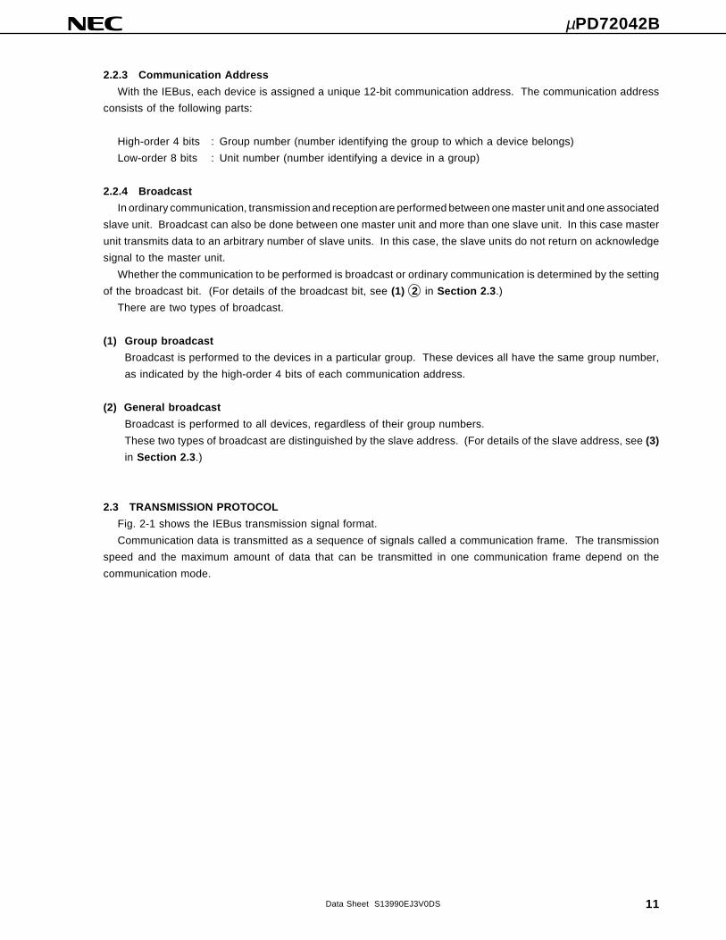
2.2.3 Communication Address
With the IEBus, each device is assigned a unique 12-bit communication address. The communication address
consists of the following parts:
High-order 4 bits : Group number (number identifying the group to which a device belongs)
Low-order 8 bits : Unit number (number identifying a device in a group)
2.2.4 Broadcast
In ordinary communication, transmission and reception are performed between one master unit and one associated
slave unit. Broadcast can also be done between one master unit and more than one slave unit. In this case master
unit transmits data to an arbitrary number of slave units. In this case, the slave units do not return on acknowledge
signal to the master unit.
Whether the communication to be performed is broadcast or ordinary communication is determined by the setting
of the broadcast bit. (For details of the broadcast bit, see (1) 2 in Section 2.3.)
There are two types of broadcast.
(1) Group broadcast
Broadcast is performed to the devices in a particular group. These devices all have the same group number,
as indicated by the high-order 4 bits of each communication address.
(2) General broadcast
Broadcast is performed to all devices, regardless of their group numbers.
These two types of broadcast are distinguished by the slave address. (For details of the slave address, see (3)
in Section 2.3.)
2.3 TRANSMISSION PROTOCOL
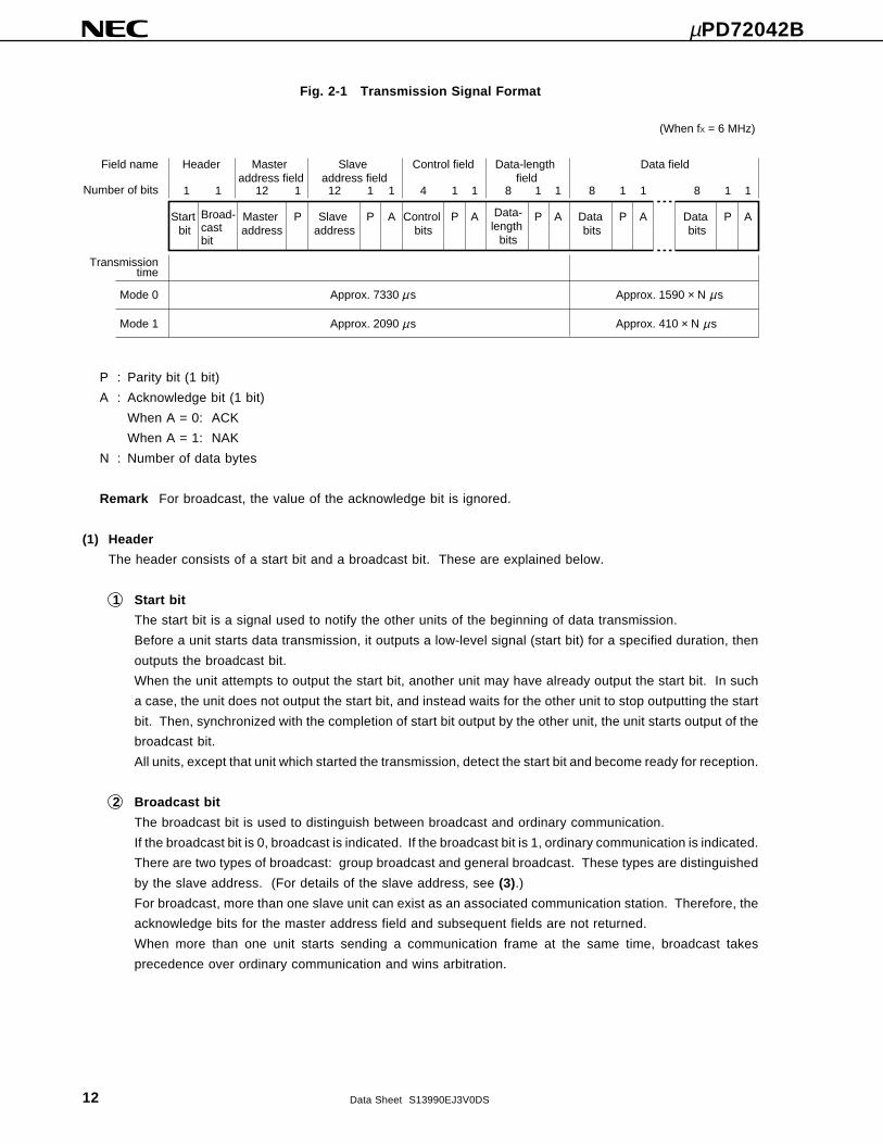
Fig. 2-1 shows the IEBus transmission signal format.
Communication data is transmitted as a sequence of signals called a communication frame. The transmission
speed and the maximum amount of data that can be transmitted in one communication frame depend on the
communication mode.
µPD72042B
12 Data Sheet S13990EJ3V0DS
Fig. 2-1 Transmission Signal Format
Field name
Number of bits
Header
1 1
Master address field
12 1
Slave address field
12 1 1
Control field
4 1 1
Data-length field
8 1 1
Data field
8 1 1 8 1 1
Start bit
Broad-castbit
Master address
P Slave address
P A Control bits
P A Data-length
bits
P A Data bits
P A Data bits
P A
Transmissiontime
Mode 0
Mode 1
(When fX = 6 MHz)
Approx. 7330
Approx. 2090
Approx. 1590 × N
Approx. 410 × N
µ s
µs
µs
µs
P : Parity bit (1 bit)
A : Acknowledge bit (1 bit)
When A = 0: ACK
When A = 1: NAK
N : Number of data bytes
Remark For broadcast, the value of the acknowledge bit is ignored.
(1) Header
The header consists of a start bit and a broadcast bit. These are explained below.
1 Start bit
The start bit is a signal used to notify the other units of the beginning of data transmission.
Before a unit starts data transmission, it outputs a low-level signal (start bit) for a specified duration, then
outputs the broadcast bit.
When the unit attempts to output the start bit, another unit may have already output the start bit. In such
a case, the unit does not output the start bit, and instead waits for the other unit to stop outputting the start
bit. Then, synchronized with the completion of start bit output by the other unit, the unit starts output of the
broadcast bit.
All units, except that unit which started the transmission, detect the start bit and become ready for reception.
2 Broadcast bit
The broadcast bit is used to distinguish between broadcast and ordinary communication.
If the broadcast bit is 0, broadcast is indicated. If the broadcast bit is 1, ordinary communication is indicated.
There are two types of broadcast: group broadcast and general broadcast. These types are distinguished
by the slave address. (For details of the slave address, see (3).)
For broadcast, more than one slave unit can exist as an associated communication station. Therefore, the
acknowledge bits for the master address field and subsequent fields are not returned.
When more than one unit starts sending a communication frame at the same time, broadcast takes
precedence over ordinary communication and wins arbitration.
µPD72042B
13Data Sheet S13990EJ3V0DS
(2) Master address field
The master address field is used to transmit the local unit address (master address) to other units.
The master address field consists of master address bits and a parity bit.
A master address consists of 12 bits. It is output starting with the MSB.
When more than one unit starts transmitting the same broadcast bit value at the same time, arbitration
determination is performed by the master address field.
Each time a unit transmits one bit of the master address field, the unit compares its output data with the data
on the bus. If the comparison indicates that the master address output by the unit differs from the data on the
bus, the unit determines that it has lost an arbitration. The unit stops transmission, and readies itself for reception.
The IEBus is organized by wired AND. When arbitration is performed between units (arbitration masters), the
unit having the smallest master address value wins the arbitration.
After the 12-bit master address has been output, only one unit is finally determined as being the master unit,
such that that unit remains in the transmission state.
Next, the master unit outputs a parity bitNote to post the master address to other units. Then, the master unit
proceeds to the slave address field.
Note Even parity is used. When the number of 1’s in the master address bits is odd, the parity bit is set to 1.
(3) Slave address field
The slave address field is used to transmit the address (slave address) of a unit (slave unit) with which the master
unit wants to communicate.
The slave address field consists of slave address bits, a parity bit, and an acknowledge bit.
A slave address consists of 12 bits. It is output starting with the MSB. After a 12-bit slave address has been
transmitted, a parity bit is output to prevent the slave address from being received incorrectly. Then, the master
unit attempts to detect the acknowledge signal from a slave unit to confirm that the slave unit exists on the bus.
When the acknowledge signal is detected, the master unit outputs a control field. Note, however, that when
performing broadcast, the master unit outputs the control field without attempting to detect the acknowledge bit.
The slave unit outputs an acknowledge signal when the slave unit recognizes a match between the slave unit’s
address and the slave address transmitted by the master unit match, and that both the master address and slave
address have even parity. If the slave unit detects odd parity, it does not recognize the addresses as matching,
so does not output an acknowledge signal. In this case, the master unit is placed in the standby (monitor) state,
and communication terminates.
For broadcast, the slave address is used to distinguish between group broadcast or general broadcast, as follows:
When the slave address is FFFH : General broadcast
When the slave address is other than FFFH : Group broadcast
Remark For group broadcast, the number of a target group is indicated by the high-order 4 bits of the slave
address.

µPD72042B
14 Data Sheet S13990EJ3V0DS
(4) Control field
The control field indicates the type and direction of the next data field.
The control field consists of control bits, a parity bit, and an acknowledge bit.
The four control bits are output starting with the MSB.
Following the control bits, a parity bit is output. If even parity is detected, and the function requested by the master
unit can be performed by the slave unit, the slave unit outputs an acknowledge signal. Then, the slave unit
proceeds to the data-length field. If the slave unit cannot perform the processing requested by the master unit,
even when even parity is detected, or if odd parity is detected, the slave unit does not output an acknowledge
signal, and it enters the standby (monitor) state again.
After detecting the acknowledge signal, the master unit proceeds to the data-length field.
If an acknowledge signal is not detected, the master unit enters the standby state, terminating communication.
For broadcast, however, the master unit proceeds to the next data-length field without attempting to detect the
acknowledge signal.
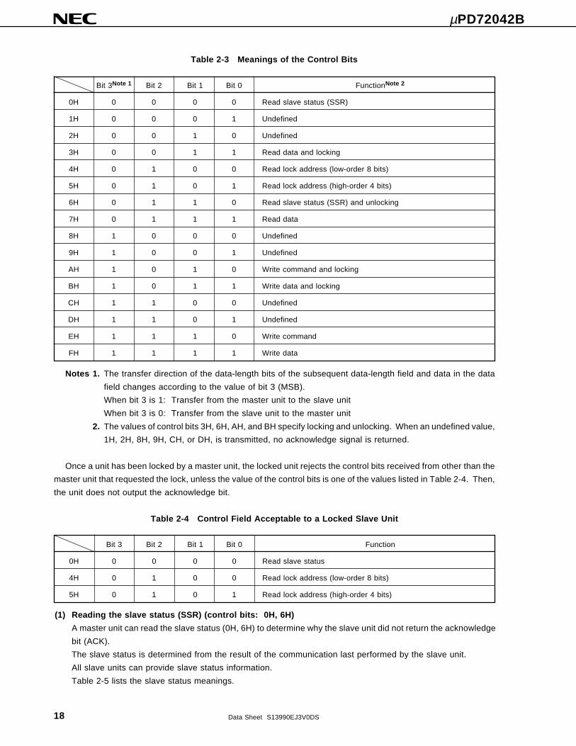
Table 2-3 lists the meanings of the control bits.
(5) Data-length field
The data-length field specifies the communication data length, in bytes.
The data-length field consists of the data-length bits, a parity bit, and an acknowledge bit.
The eight data-length bits are output starting with the MSB. The data-length bits indicate the communication
data length, in bytes, as shown in Table 2-2.
Table 2-2 Values of the Data-Length Bits and Their Meanings
Data-length bit (hexadecimal) Transmission data length, in bytes
01H 1
02H 2
: :
: :
FFH 255
00H 256
Remark If the data length set in the data-length bits exceeds the maximum number of transmission bytes, the
latter varying with the communication mode, more than one frame is transmitted. In the second and
subsequent frames, the data-length bits indicate the remaining communication data length, in bytes.
The operation performed for this field differs depending on whether master transmission (when bit 3 of the control
bits is 1) or master reception (when bit 3 of the control bits is 0) is performed.
1 Master transmission
The data-length bits and parity bit are output by the master unit. When the slave unit detects even parity,
the slave unit outputs an acknowledge signal, then proceeds to the data field. For broadcast,
however, the slave unit does not output an acknowledge signal.
If the slave unit detects odd parity, the slave unit does not output an acknowledge signal, regarding the
received data-length bits as being incorrect. Then, the slave unit enters the standby (monitor) state again.
At this time, the master unit also enters the standby state again, and communication terminates.
µPD72042B
15Data Sheet S13990EJ3V0DS
2 Master reception
The data-length bits and parity bit are output by the slave unit. When the master unit detects even parity,
the master unit outputs the acknowledge signal.
If the master unit detects odd parity, the master unit does not output an acknowledge signal, regarding the
received data-length bits as being incorrect. Then, the master unit enters the standby state again. At this
time, the slave unit also enters the standby state again, and communication terminates.
(6) Data field
The data field is used for data transmission and reception to and from a slave unit.
The master unit uses the data field to transmit data to the slave unit, or to receive data from the slave unit.
The data field consists of data bits, a parity bit, and an acknowledge bit.
The eight data bits are output, starting with the MSB.
After the data bits have been output, the parity bit and acknowledge bit are output from the master unit and slave
unit, respectively.
Broadcast is performed only when the master unit transmits data. At this time, any acknowledge signal is ignored.
The operations related to master transmission and master reception are explained below.
1 Master transmission
When the master unit performs a write to a slave unit, the master unit transmits the data bits and a parity
bit to the slave unit. The slave unit receives the data bits and parity bit, then outputs an acknowledge signal
if even parity is detected and the reception buffer is empty. If odd parity is detected, or if the reception buffer
is not empty, the slave unit rejects the corresponding data, and does not output an acknowledge signal.
If no acknowledge signal is received from the slave unit, the master unit transmits the same data
again. The master unit repeats this operation until it receives an acknowledge signal from the slave unit,
or until the data exceeds the maximum number of transmission bytes.
When even parity is detected, and an acknowledge signal is received from the slave unit, the master unit
transmits the subsequent data, if any, and provided the maximum number of transmission bytes is not
reached.
For broadcast, an acknowledge signal is not output by any slave unit. The master unit transfers data one
byte at a time.
2 Master reception
When the master unit reads data from a slave unit, the master unit outputs a synchronization signal for each
bit as it is read.
The slave unit outputs data and a parity bit to the bus according to the synchronization signal output by the
master unit.
The master unit reads the data and parity bit output by the slave unit, and checks the parity.
If the master unit detects odd parity, or if the reception buffer is not empty, the master unit rejects the data,
and does not output an acknowledge signal. The master unit repeats the read operation for the same data
provided the maximum allowable number of transmission bytes per communication frame has not been
reached.
If the master unit confirms even parity, and the reception buffer is empty, the master unit accepts the data,
and returns an acknowledge signal to the slave unit. Then, the master unit reads the next data, provided
the maximum allowable number of transmission bytes per frame has not been reached.
µPD72042B
16 Data Sheet S13990EJ3V0DS
(7) Parity bit
A parity bit is used to check for errors in the transmission data.
A parity bit is added to the master address bits, slave address bits, control bits, data-length bits, and data bits.
Even parity is used. If the number of 1’s in the data is odd, the parity bit is set to 1. If the number of 1’s in the
data is even, the parity bit is set to 0.
(8) Acknowledge bit
In ordinary communication (one-unit-to-one-unit communication), an acknowledge bit is added in the following
positions to confirm that data has been received correctly:
• At the end of the slave address field
• At the end of the control field
• At the end of the data-length field
• At the end of the data field
The acknowledge bit is defined as follows:
• 0: Indicates that transmission data has been recognized. (ACK)
• 1: Indicates that no transmission data has been recognized. (NAK)
For broadcast, the acknowledge bit is ignored.
1 Acknowledge bit at the end of the slave address field
If any of the following is detected, the acknowledge bit at the end of the slave address field is set to NAK,
and transmission is stopped:
• The parity of the master address bits or slave address bits is incorrect.
• A timing error occurred (bit format error).
• No slave unit is found.
2 Acknowledge bit at the end of the control field
If any of the following is detected, the acknowledge bit at the end of the control field is set to NAK, and
transmission is stopped:
• The parity of the control bits is incorrect.
• Although the slave reception bufferNote is not empty, bit 3 of the control bits is 1 (write operation).
• Although the slave transmission bufferNote is empty, the control bits indicate data read (3H, 7H).
• For a locked unit, a unit other than the unit that specified the lock makes a request by using control bits
indicating 3H, 6H, 7H, AH, BH, EH, or FH.
• Although no lock has been set, control bits indicating lock address read (4H) are set.
• A timing error occurred.
• An undefined control bit setting has been made.
Note See (1) in Section 2.4.
µPD72042B
17Data Sheet S13990EJ3V0DS
3 Acknowledge bit at the end of the data-length field
If any of the following is detected, the acknowledge bit at the end of the data-length field is set to NAK, and
transmission is stopped:
• The parity of the data-length bits is incorrect.
• A timing error occurred.
4 Acknowledge bit at the end of the data field
If any of the following is detected, the acknowledge bit at the end of the data field is set to NAK, and
transmission is stopped:
• The parity of the data bits is incorrectNote.
• A timing error occurred after the previous acknowledge bit.
• The reception buffer is full, such that no more data can be acceptedNote.
Note In this case, if the maximum allowable number of transmission bytes per frame has not yet been reached,
the transmitter retries transmission of the data field until the maximum number of transmission bytes is
reached.
2.4 TRANSMISSION DATA (CONTENTS OF THE DATA FIELD)
The contents of the data field are indicated by the control bits.
µPD72042B
18 Data Sheet S13990EJ3V0DS
Table 2-3 Meanings of the Control Bits
Bit 3Note 1 Bit 2 Bit 1 Bit 0 FunctionNote 2
0H 0 0 0 0 Read slave status (SSR)
1H 0 0 0 1 Undefined
2H 0 0 1 0 Undefined
3H 0 0 1 1 Read data and locking
4H 0 1 0 0 Read lock address (low-order 8 bits)
5H 0 1 0 1 Read lock address (high-order 4 bits)
6H 0 1 1 0 Read slave status (SSR) and unlocking
7H 0 1 1 1 Read data
8H 1 0 0 0 Undefined
9H 1 0 0 1 Undefined
AH 1 0 1 0 Write command and locking
BH 1 0 1 1 Write data and locking
CH 1 1 0 0 Undefined
DH 1 1 0 1 Undefined
EH 1 1 1 0 Write command
FH 1 1 1 1 Write data
Notes 1. The transfer direction of the data-length bits of the subsequent data-length field and data in the data
field changes according to the value of bit 3 (MSB).
When bit 3 is 1: Transfer from the master unit to the slave unit
When bit 3 is 0: Transfer from the slave unit to the master unit
2. The values of control bits 3H, 6H, AH, and BH specify locking and unlocking. When an undefined value,
1H, 2H, 8H, 9H, CH, or DH, is transmitted, no acknowledge signal is returned.
Once a unit has been locked by a master unit, the locked unit rejects the control bits received from other than the
master unit that requested the lock, unless the value of the control bits is one of the values listed in Table 2-4. Then,
the unit does not output the acknowledge bit.
Table 2-4 Control Field Acceptable to a Locked Slave Unit
Bit 3 Bit 2 Bit 1 Bit 0 Function
0H 0 0 0 0 Read slave status
4H 0 1 0 0 Read lock address (low-order 8 bits)
5H 0 1 0 1 Read lock address (high-order 4 bits)
(1) Reading the slave status (SSR) (control bits: 0H, 6H)
A master unit can read the slave status (0H, 6H) to determine why the slave unit did not return the acknowledge
bit (ACK).
The slave status is determined from the result of the communication last performed by the slave unit.
All slave units can provide slave status information.
Table 2-5 lists the slave status meanings.
µPD72042B
19Data Sheet S13990EJ3V0DS
Fig. 2-2 Slave Status (SSR) Bit Format
MSB
bit 7 bit 6 bit 5 bit 4 bit 3 bit 2 bit 1 bit 0
LSB
Table 2-5 Slave Status Meanings
Bit Value Meaning
Bit 0Note 1 0 The slave transmission buffer is empty.
1 The slave transmission buffer is not empty.
Bit 1Note 2 0 The slave reception buffer is empty.
1 The slave reception buffer is not empty.
Bit 2 0 The unit is not locked.
1 The unit is locked.
Bit 3 0 Fixed at 0
Bit 4Note 3 0 Slave transmission disabled
1 Slave transmission enabled
Bit 5 0 Fixed at 0
Bit 7 00 Mode 0
Bit 6 01 Mode 1
10 Reserved for future expansion
11
Indicates the highest
mode supported by the
unitNote 4.
Notes 1. The slave transmission buffer is accessed during a data read operation (control bits: 3H, 7H).
For the µPD72042B, this buffer corresponds to the TBF available when STRQ of the FLG register is set
to 1.
2. The slave reception buffer is accessed during a data write operation (control bits: 8H, AH, BH, EH, FH).
For the µPD72042B, this buffer corresponds to the RBF available when SLRE of the FLG register is set
to 1.
3. The value of bit 4 can be selected by using the UAR1 register.
4. Bits 7 and 6 are currently fixed to 10 in the hardware of the µPD72042B.
(2) Data/command transfer (control bits: Read (3H, 7H), write (AH, BH, EH, FH))
When data read (3H, 7H) is set, the data in the data buffer of the slave unit is read into the master unit.
When data write (BH, FH) or command write (AH, EH) is set, the data received by the slave unit is processed
according to the operation specifications for the slave unit.
Remarks 1. The user can select data and commands as necessary according to the system.
2. 3H, AH, and BH may cause locking, depending on the communication conditions and status.

µPD72042B
20 Data Sheet S13990EJ3V0DS
(3) Reading a lock address (control bits: 4H, 5H)
When a lock address read operation (4H, 5H) is specified, the address (12 bits) of the master unit that
issued the lock instruction is read in one-byte form, as shown below.
Fig. 2-3 Lock Address Format
MSB LSB
Control bits : 4H
Control bits : 5H
Low-order 8 bits
Undefined High-order 4 bits
(4) Locking and unlocking (control bits: Locking (3H, AH, BH), unlocking (6H))
The lock function is used to enable the transfer a message using more than one communication frame.
When locked, a unit cannot receive data from other than the unit that requested the lock.
Locking and unlocking are performed as follows:
1 Locking
The master unit can lock the slave unit by specifying the lock with the corresponding control bits (3H, AH,
BH). In this case, when the transmission or reception of acknowledge bit 0 for the data-length field has been
completed, but the communication frame is then terminated before transmission or reception of as many data
bytes as are specified by the data-length bits is completed, the slave unit is locked. At this time, the bit
indicating the lock status (bit 2) in the slave status byte is set to 1.
2 Unlocking
The master unit can unlock a locked slave unit when the control bits specify locking (3H, AH, or BH) or
unlocking (6H). The slave unit is unlocked once as many data bytes as are specified by the data-length bits
have been transmitted or received within one communication frame. At this time, the bit indicating the lock
status (bit 2) in the slave status byte is reset to 0.
For broadcast, locking or unlocking is not performed.
µPD72042B
21Data Sheet S13990EJ3V0DS
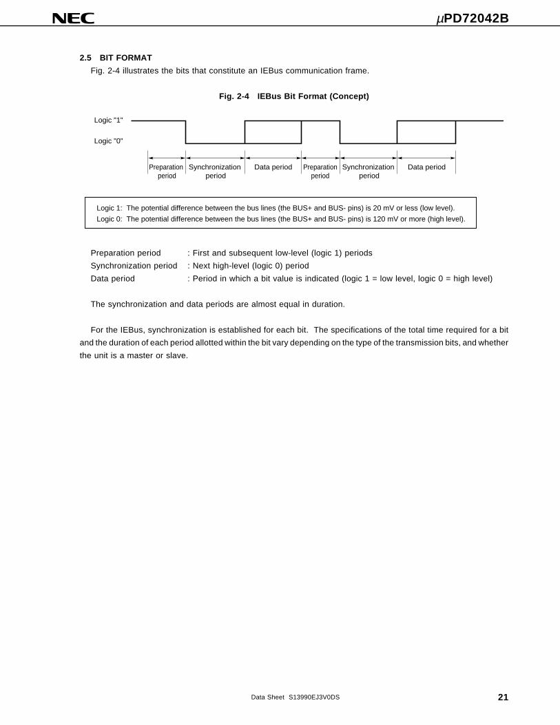
2.5 BIT FORMAT
Fig. 2-4 illustrates the bits that constitute an IEBus communication frame.
Fig. 2-4 IEBus Bit Format (Concept)
Logic "1"
Logic "0"
Preparation period
Synchronization period
Data period Preparationperiod
Synchronization period
Data period
Logic 1: The potential difference between the bus lines (the BUS+ and BUS- pins) is 20 mV or less (low level).
Logic 0: The potential difference between the bus lines (the BUS+ and BUS- pins) is 120 mV or more (high level).
Preparation period : First and subsequent low-level (logic 1) periods
Synchronization period : Next high-level (logic 0) period
Data period : Period in which a bit value is indicated (logic 1 = low level, logic 0 = high level)
The synchronization and data periods are almost equal in duration.
For the IEBus, synchronization is established for each bit. The specifications of the total time required for a bit
and the duration of each period allotted within the bit vary depending on the type of the transmission bits, and whether
the unit is a master or slave.
µPD72042B
22 Data Sheet S13990EJ3V0DS
3. MICROCOMPUTER INTERFACE
3.1 TRANSFER METHOD
Either of two microcomputer interface modes can be selected: three-wire serial I/O mode or two-wire serial I/O
mode.
Whether three-wire serial I/O mode or two-wire serial I/O mode is selected depends on the input level of the SEL
pin (pin 12). (See Section 3.3 for details.)
SEL ← 1: Three-wire serial I/O
SEL ← 0: Two-wire serial I/O
(1) Three-wire serial I/O (SEL ← 1)
Three wires are used to read and write data. The three wires are the serial clock input (SCK), serial data input
(SINote 1), and serial data output (SONote 2).
(a) Read operation
Data is output to the SO pin upon detecting the falling edge of the SCK pin.
(b) Write operation
Data is input via the SI pin upon detecting the rising edge of the SCK pin. At this time, 1 is output on the
SO pin.
(2) Two-wire serial I/O (SEL ← 0)
Two wires are used to read and write data. The two wires are the serial clock input (SCK) and serial data I/O
(SIONote 1).
(a) Read operation
The SIO pin is placed in the output state, and data is output upon detecting the falling edge of the SCK pin.
(b) Write operation
The SIO pin is placed in the input state, and data is input upon detecting the rising edge of the SCK pin.
Notes 1. The SI pin for three-wire serial I/O mode is also used as the SIO pin for two-wire serial I/O mode.
2. The impedance of the SO pin for three-wire serial I/O mode goes high in two-wire serial I/O mode. So,
connect the SO pin to GND or VDD.

µPD72042B
23Data Sheet S13990EJ3V0DS
I : Input state Hi-Z : High-impedance state
O : Output state × : Don’t care
O* : State in which 1 is output
3.2 DATA TRANSFER FORMAT
3.2.1 Three-Wire Data Transfer (SEL = 1)
(1) Control mode
When the C/D input is set high, control mode is set to control data transfer. Data transfer control involves the
following processing.
1 Register address setting
2 Register read/write selection
Remark After reset (RESET) cancellation, the state enabling writing to the register at address 0000B is set.
Caution In control mode, each data item is read every eighth clock pulse. (Data of less than eight clock
periods is ignored.)
Table 3-1 I/O States of the SIO (SI) and SO Pins
RESET CS SEL C/D SI (SIO) SO State
Three-wire/two-wire Operating mode
0 × × × I Hi-Z – Reset state
1 1 × × I Hi-Z – Chip nonselected state
1 0 1 1 I O* Three-wire Control mode
0 Data write mode
O Data read mode
0 1 I Hi-Z Two-wire Control mode
0 Data write mode
O Data read mode
C/D
SCK
SI A3A2A1A0R/
W
× × ×
µPD72042B
24 Data Sheet S13990EJ3V0DS
(2) Data read mode
When the C/D pin is set low after register read is selected in control mode, the data read mode is set. In data
read mode, the data in a read register is read on the SO pin upon detecting the falling edge of the SCK pin.
C/D
SCK
SI A0 A1 A2 A3× × ×
D0 D1 D2 D3 D4 D5 D6 D7SO
StateControl mode
(selection of register read) Data read mode
Serial clock counterreset pointer
“1”
1
Caution When the C/D pin is set high in data read mode, the serial clock counter is reset. Therefore, the
remaining bits of the byte cannot be read; at the next falling edge, read is performed starting from
the next byte in the case of RBF, or from the first bit for other registers.
(3) Data write mode
When the C/D pin is set low after register write has been selected in control mode, data write mode is set. In
data write mode, data for a write register is applied to the SI pin at the rising edge of the SCK pin.
C/D
SCK
SI A0 A1 A2 A3× × × D0 D1 D2 D3 D4 D5 D6 D7
SO
0
StateControl mode
(selection of register write) Data write mode
Serial clock counterreset pointer
“1”
Caution Register overwrite is started immediately after the eighth clock rising edge. All registers other
than TBF are overwritten on the eighth clock rising edge. (Data of less than eight clock periods
is ignored.)
µPD72042B
25Data Sheet S13990EJ3V0DS
3.2.2 Two-Wire Data Transfer (SEL = 0)
(1) Control mode
When the C/D input is set high, control mode is set to control data transfer. Data transfer control involves the
following processing.
1 Register address setting
2 Register read/write selection
C/D
SCK
SIOR/
W× × × A0 A1 A2 A3
Remark After reset (RESET) cancellation, the state enabling writing to the register at address 0000B is set.
Caution In control mode, each data item is read every eighth clock pulse. (Data of less than eight clock
periods is ignored.)
(2) Data read mode
C/D
SCK
SIONote A0 A1 A2 D0 D1 D2 D3 D4 D5 D6 D71× × × A3
Serial clock counterreset pointer
Control mode(selection of register read) Data read modeState
Note SIO pin input state
SIO pin output state
Cautions 1. When the C/D pin is set high in data read mode, the serial clock counter is reset. Therefore,
the remaining bits of the byte cannot be read; at the next falling edge, a read operation is
performed starting from the next byte in the case of RBF, or from the first bit for other registers.
2. The SIO pin is a CMOS I/O pin. So, be careful to avoid an output collision between the SIO
pin and the microcomputer. Further, a pull-up resistor is required when N-ch open-drain
output of the microcomputer is used. Note that if the last output level is low upon the
termination of read mode, current will flow constantly.
µPD72042B
26 Data Sheet S13990EJ3V0DS
(3) Data write mode
C/D
SCK
SIONote A0 A1 A2 A3× × × D0 D1 D2 D3 D4 D5 D6 D70
State Data write modeControl mode
(selection of register write)
Serial clock counterreset pointer
Note SIO pin input state
Caution Register overwrite is started immediately after the eighth clock rising edge. All registers other
than TBF are overwritten at the eighth clock rising edge. (Data of less than eight clock periods
is ignored.)

µPD72042B
27Data Sheet S13990EJ3V0DS
3.3 CONNECTION TO A MICROCOMPUTER
(1) Three-wire serial I/O
(2) Two-wire serial I/O
Notes 1. When only the µPD72042B is to be controlled from a microcomputer via a serial I/O interface, the CS
pin must be tied low (by connecting it to GND).
2. When an interrupt is detected by polling (in FLG register read), IRQ may be left open. When high-volume
or high-speed data transfer is required, however, the system described above is recommended to ensure
reliable data transfer.
3. Required when the microcomputer’s N-ch open-drain output is used. The SIO pin of the µPD72042B
is a CMOS I/O pin.
120 Ω
5 V
VDD
AVDD
TEST
BUS+
BUS–
XI
XO
GND
SEL
CSNote 1
C/D
SCK
SI
SO
IRQNote 2
RESET
Output port
Output port
SCK
SO
SI
INTLow voltage detection circuit
75XL series78K series
180 Ω
180 Ω 6 MHz
120 Ω
5 V
PD72042B
Microcomputer
µ
Microcomputer
120 Ω
5 V
180 Ω
180 Ω 6 MHz
120 Ω
75XL series78K series
Lowvoltagedetection circuit
VDD
AVDD
TEST
BUS+
BUS–
XI
XO
GND
SEL
CSNote 1
C/D
SCK
SIOSO
IRQNote 2
RESET
Output port
Output port
SCK
SIO
INT
Note 3
PD72042Bµ
5 V
µPD72042B
28 Data Sheet S13990EJ3V0DS
3.4 STANDBY MODE SETTING AND CANCELLATION
Standby mode can be set by setting STREQ of the CTR register to 1. The XI pin for oscillation is tied to GND,
and the impedance of the XO pin goes high.
In standby mode (with the STM flag of the FLG register set to 1), only the following registers can be accessed:
Writable register : CTR (address 0000B)
Readable register : FLG (address 0001B)
Standby mode can be cancelled by setting STREQ of the CTR register to 0.
Caution Do not read any data from internal registers via the serial I/O during the period from when a
microcomputer sets the STREQ flag to 1 to when the µµµµµPD72042B enters the standby mode. This
period is one-communication frame at maximum.
3.5 RESET MODE SETTING AND CANCELLATION
For hardware reset, the registers are initialized and standby mode is set. (During this period, oscillation is stopped.)
For software reset, the registers are initialized, and operation is started.
µPD72042B
29Data Sheet S13990EJ3V0DS
4. REGISTERS
A microcomputer controls IEBus communication by reading from and writing to the internal registers of the
µPD72042B.
Registers are classified into write registers and read registers. The total size of the write registers is 40 bytes;
the transmission buffer uses 33 of the 40 bytes. The total size of the read registers is 49 bytes; the reception buffer
uses 40 of the 49 bytes.
Table 4-1 lists the registers.
µPD72042B
30 Data Sheet S13990EJ3V0DS
Address Name High-order 4 bits Low-order 4 bits Note Reference page
0H 0000 CTR – – – REEN SRST – – STREQ A p. 31
1H 0001 CMR 0 LOCK BUFC COMC C p. 32
1 0 0 0 0 IRS MFC DERC
2H 0010 UAR1 Local station address Condition code B p. 34 (low-order 4 bits)
3H 0011 UAR2 Local station address (high-order 8 bits) B p. 34
4H 0100 SAR1 Slave address 0 0 0 0 D p. 35 (low-order 4 bits)
5H 0101 SAR2 Slave address (high-order 8 bits) D p. 35
6H 0110 MCR Broadcast bits Number of Control bits D p. 36 arbitrations
7H 0111 – – – –
8H 1000 – – – –
EH 1110 TBF Number of bytes of transmission data, transmission data F p. 38
Table 4-1 µPD72042B Registers
(a) Write registers
(b) Read registers
Address Name High-order 4 bits Low-order 4 bits Note Reference page
0H 0000 STR TFL TEP RFL REP – A p. 39
1H 0001 FLG – MARQ STRQ SLRE CEX RAW STM IRQ A p. 40
2H 0010 RDR1 Number of bytes of master reception data A p. 42
3H 0011 RDR2 Number of bytes of slave reception data or A p. 42broadcast reception data
4H 0100 LOR1 Lock address (low-order 8 bits) H p. 43
5H 0101 LOR2 Lock state Lock address H p. 43(high-order 4 bits)
6H 0110 DAR1 Broadcast address – E p. 44(low-order 4 bits)
7H 0111 DAR2 Broadcast address (high-order 8 bits) E p. 44
8H 1000 RCR Return codes (MARC, SLRC) A p. 45
EH 1110 RBF Transmitter address, reception data G p. 57
Note Writable and readable periods of the registers of the µPD72042B
A: ArbitraryB: After system reset cancellationC: While CEX of the FLG register (address 0001) is set to 0
D: While MARQ of the FLG register (address 0001) is set to 0E: After SLRC of the RCR register (address 1000) is set to 1100 (broadcast reception error)F: While TFL of the STR register (address 0000) is set to 0
G: While REP of the STR register (address 0000) is set to 0H: When CEX of the FLG register (address 0001) is set to 0 after LOCK of the CMR register (address 0001)
is set to 1

µPD72042B
31Data Sheet S13990EJ3V0DS
Cautions 1. In standby mode (with STM of the FLG register set to 1), the user can only write to the CTR
register (including standby mode cancellation) and read from the FLG register.
2. Never access a free address.
3. Slave status (SSR) can be read into RBF by setting the control bits to 0H or 6H from the master
unit.
CTR Address : 0000B (0H)
Read/write : Write
Control register When reset : ×××00××1B
CTR is a one-byte write register used to control µPD72042B operations.
b7
—
b6
—
b5
—
b4 b3 b0
— CTR
b2 b1
REEN SRST — STREQ
[REEN]
When REEN is set to 1, the SLRE flag of the FLG register is immediately set to 1 to enable both slave and broadcast
reception.
[SRST]
When SRST is set to 1, the µPD72042B is immediately reset. (Note, however, that STREQ is set to a written value.)
[STREQ]
1: Requests standby mode.
0: Exits from standby mode.
• Standby mode setting and cancellation
The µPD72042B is requested to enter the standby mode by setting the STREQ flag to 1 from the microcomputer.
The µPD72042B enters standby mode when the standby mode input enabled state (carrier sense state) is set. In
this case, the impedance of the BUS+ and BUS– pins goes high (logic 1), and the STM flag of the FLG register
is set to 1. In standby mode, oscillation is stopped, and all operations are stopped while preserving the internal
data, thus minimizing power consumption.
When, in standby mode, the STREQ flag is set to 0 from the microcomputer, standby mode is cancelled
after the period (about 20 ms at fX = 6 MHz) needed for oscillation to stabilize; the halted operations are resumed
from the point at which standby mode was set. At this time, the STM flag of the FLG register changes to 0.
In standby mode, only writing to the CTR register (for standby mode cancellation) and reading from the FLG register
can be performed from the microcomputer.
Cautions 1. When the SRST flag and STREQ flag are simultaneously set to 1, standby mode is set after
software reset. (This state is the same as that set by hardware reset.) Note, however, that
when the SRST flag is set to 1 in standby mode, a software reset is performed, but this is not
reflected in the FLG register.
2. Do not read any data from internal registers via the serial I/O during the period from when a
microcomputer sets the STREQ flag to 1 to when the µµµµµPD72042B enters the standby mode.
This period is one-communication frame at maximum.

µPD72042B
32 Data Sheet S13990EJ3V0DS
CMR Address : 0001B (1H)
Read/write : Write
Command register When reset : 00000000B
CMR is a one-byte write register used to set a command for communication control, transmission/reception buffer
control, or optional function setting.
When data is set in CMR from the microcomputer, CEX of the FLG register is set to 1. When the µPD72042B
processes the data set in CMR, CEX is set to 0.
After the microcomputer checks that CEX of the FLG register is set to 0, new data can be set in CMR.
The following describes the data that is set in CMR.
(1) When bit 7 (MSB) of CMR is 0
b7
0
b6
LOCK
b5
BUFC
b4 b3 b0
COMC CMR
[LOCK]: Lock state setting command
1 : The value representing the lock state (0001 for locked or 0000 for not-locked) and lock address are output
to LOR1 and LOR2. Note, however, that when 0000 (not-locked) is output, any lock address value is ignored.
0 : The contents of LOR1 and LOR2 remain as is.
[BUFC]: Transmission/reception buffer control command
00 : The transmission and reception buffers remain as is.
01 : The transmission buffer (TBF) is cleared.
10 : The reception buffer (RBF) is cleared.
11 : The data of the previous (latest) communication frame to be stored in the reception buffer (RBF) is
clearedNote 1.
[COMC]: Communication control command
0000: Communication operation remains as is.
0001: The locked state is cancelled.
1000: Master communication is requestedNote 2.
1001: Master communication is requested, with the previous master transmission state heldNote 3.
1010: Master communication is aborted.
1011: Slave data transmission is requestedNote 4.
1100: Slave data transmission is requested, with the previous slave data transmission state heldNote 5.
1101: Slave data transmission is aborted.
1111: Slave reception and broadcast reception are disabled.
Notes 1. If the microcomputer has already read the data for the previous (latest) communication frame from RBF,
or optional function setting in CMR is selected and MFC = 0, clear RBF with BUFC = 10.

µPD72042B
33Data Sheet S13990EJ3V0DS
Notes 2. When the MSB of the control bits set in MCR is 1 (for master transmission), set the number of bytes
of transmission data, and at least one byte of transmission data in TBF before command setting.
3. When the MSB of the control bits set in MCR is 1 (for master transmission), set at least one byte of
transmission data before command setting. This operation is not required if all transmission data has
already been set in TBF.
4. Set the number of bytes of transmission data, and at least one byte of transmission data in TBF before
command setting.
5. Set at least one byte of transmission data in TBF before command setting. This operation is not required
if all transmission data has already been set in TBF.
(2) When bit 7 (MSB) of CMR is 1
An optional function is set.
b7
1
b6
0
b5
0
b4 b3 b0
IRS CMR
b2 b1
0 0 MFC DERC
[MFC]: Selection of one frame/multiple frames
1 : Data for multiple frames is stored in RBF.
0 : Data for only one frame is stored in RBF.
[DERC]: Broadcast reception selection
1 : The issue of return code 1100 (broadcast reception error) for SLRC of the RCR register is enabled.
0 : The issue of return code 1100 (broadcast reception error) for SLRC of the RCR register is disabled.
[IRS]: Interrupt generation condition selection
0 : An interrupt is requested when the data of the RCR register changes.
1 : An interrupt is requested when the data of the RCR register changes to other than the following:
MARC = 0000B (start of master transmission)
MARC = 0100B (start of master reception)
SLRC = 0000B (start of slave data transmission)
SLRC = 0100B (start of slave reception)
SLRC = 1000B (start of broadcast reception)
Caution Set an optional function in initialization processing after reset cancellation for the µPD72042B.
Until an optional function has been set, the µPD72042B will not accept IEBus communication.
µPD72042B
34 Data Sheet S13990EJ3V0DS
UAR1 Address : 0010B (2H) (UAR1)
UAR2 0011B (3H) (UAR2)
Read/write : Write
Local station unit address register When reset : Undefined (with the
previous data held)
UAR1 and UAR2 are registers used to set a local station unit address (12 bits) and condition code.
Set UAR1 and UAR2 after reset cancellation.
b7
Local station address (low-order 4 bits)
b4 b3 b0
Condition code UAR1
b7 b0
Local station address (high-order 8 bits) UAR2
[Local station address]
A local station address is used as a master address when the local station performs communication as the master
unit. A local station address is used as a slave address when the local station performs communication as a slave.
[Condition code]
Bit position Condition code Condition setting
b3, b2 00 Communication is performed in mode 0.
01 Communication is performed in mode 1.
10 Undefined
11
b0 0 The slave transmission section is disabled.
1 The slave transmission section is enabled.
Remark Bit 1 of a condition code is not used. (Set the bit to either 0 or 1.)
µPD72042B
35Data Sheet S13990EJ3V0DS
SAR1 Address : 0100B (4H) (SAR1)
SAR2 0101B (5H) (SAR2)
Read/write : Write
Slave address register When reset : Undefined (the pre-
vious data is held)
The SAR1 and SAR2 registers are used to set the address of a remote station (slave address) in master
communication.
Set SAR1 and SAR2 while the value of MARQ of the FLG register is 0 (while master communication is not
requested).
b7
Slave address (low-order 4 bits)
b4 b3 b0
SAR1
b7 b0
Slave address (high-order 8 bits) SAR2
0 0 0 0
µPD72042B
36 Data Sheet S13990EJ3V0DS
MCR Address : 0110B (6H)
Read/write : Write
Master communication register When reset : Undefined (the pre-
vious data is held)
The MCR register is used to set a master communication condition.
Set MCR while the value of MARQ of the FLG register is 0 (while master communication is not requested).
b7
Broadcast bit
b6
Number of arbitrations
b4 b3 b0
Control bits MCR
[Broadcast bit]
This bit is used to select broadcast or separate communication.
Bit 7 = 0: Broadcast
Bit 7 = 1: Separate communication
[Number of arbitrations] (Number of retries)
This field is used to set the maximum number of retry operations to be performed if arbitration is lost in master
communication. The µPD72042B automatically retries communication as many times as the number set in this field.
b6 b5 b4 Number of retries
0 0 0 0
0 0 1 1
0 1 0 2
0 1 1 3
1 0 0 4
1 0 1 5
1 1 0 6
1 1 1 7
µPD72042B
37Data Sheet S13990EJ3V0DS
[Control bits]
This control field is used to set the control bits (four bits).
• Contents of control bits
Bit 3Note 1 Bit 2 Bit 1 Bit 0 FunctionNote 2
0H 0 0 0 0 Slave status (SSR) read
1H 0 0 0 1 Undefined
2H 0 0 1 0 Undefined
3H 0 0 1 1 Data read and lock
4H 0 1 0 0 Lock address read (low-order 8 bits)
5H 0 1 0 1 Lock address read (high-order 4 bits)
6H 0 1 1 0 Slave status (SSR) read and unlock
7H 0 1 1 1 Data read
8H 1 0 0 0 Undefined
9H 1 0 0 1 Undefined
AH 1 0 1 0 Command write and lock
BH 1 0 1 1 Data write and lock
CH 1 1 0 0 Undefined
DH 1 1 0 1 Undefined
EH 1 1 1 0 Command write
FH 1 1 1 1 Data write
Notes 1. The value of bit 3 (MSB) determines the transfer direction of the subsequent data-length field data and
data field data.
When bit 3 is set to 1: Data is transferred from the master unit to a slave unit.
When bit 3 is set to 0: Data is transferred from a slave unit to the master unit.
2. 3H, 6H, AH, and BH are control bits used for lock setting and cancellation.
When an undefined value of 1H, 2H, 8H, 9H, CH, or DH is sent, no acknowledgement is returned.
µPD72042B
38 Data Sheet S13990EJ3V0DS
TBF Address : 1110B (EH)
Read/write : Write
Transmission buffer When reset : Empty
TBF is a 33-byte FIFO buffer used to hold the number of bytes of transmission data and transmission data for master
transmission and slave data transmission.
TBF can be written from the microcomputer when the TFL flag of the STR register is set to 0 (indicating that TBF
is not full).
In master transmission and slave data transmission, the following format is used to load data into TBF from the
microcomputer.
Byte 1 Number of bytes of transmission data
Byte 2 First byte of transmission data
Byte 3 Second byte of transmission data
Byte 33
……
…
[Byte 1]: Number of bytes of transmission data
Between 1 and 256 bytes can be set.
[Bytes 2 and up]: Transmission data
As much transmission data as is set in byte 1 is set in byte 2 and subsequent bytes.
TBF
Number of bytes of Data set in byte 1 of TBF
transmission data
1 01H
2 02H
255 FFH
256 00H
……
……
µPD72042B
39Data Sheet S13990EJ3V0DS
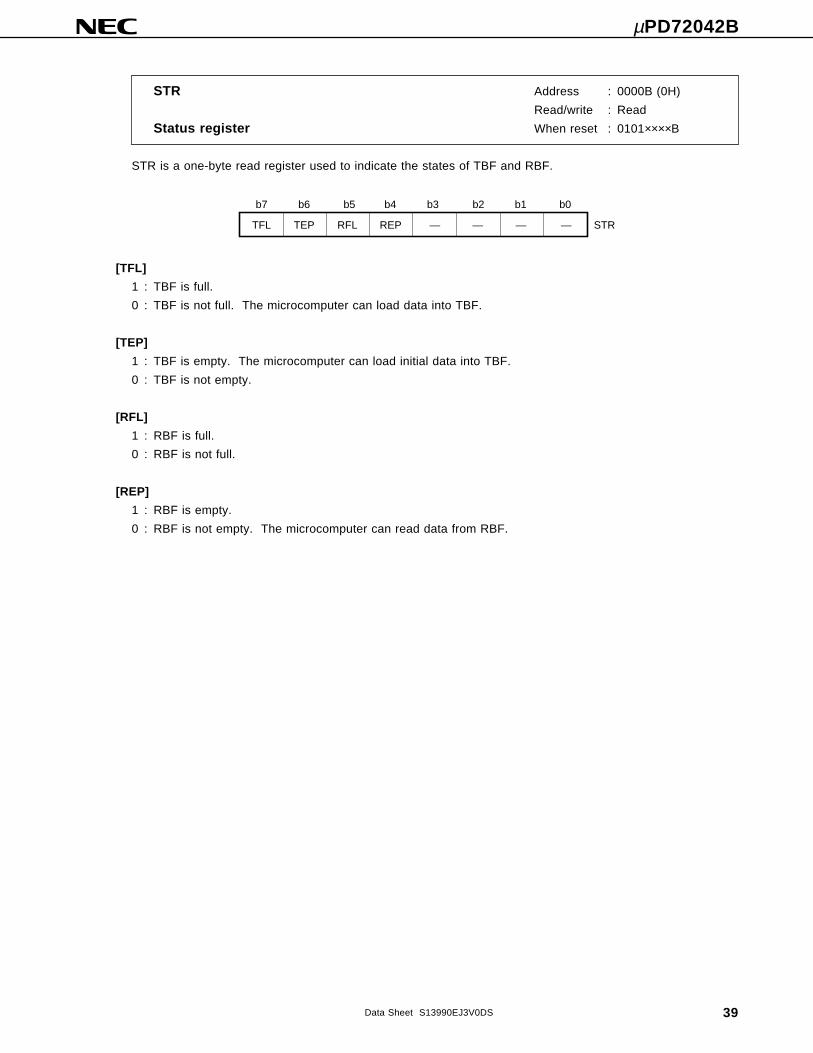
STR Address : 0000B (0H)
Read/write : Read
Status register When reset : 0101××××B
STR is a one-byte read register used to indicate the states of TBF and RBF.
b7
TFL
b6
TEP
b5
RFL
b4 b3 b0
— STR
b2 b1
REP — — —
[TFL]
1 : TBF is full.
0 : TBF is not full. The microcomputer can load data into TBF.
[TEP]
1 : TBF is empty. The microcomputer can load initial data into TBF.
0 : TBF is not empty.
[RFL]
1 : RBF is full.
0 : RBF is not full.
[REP]
1 : RBF is empty.
0 : RBF is not empty. The microcomputer can read data from RBF.
µPD72042B
40 Data Sheet S13990EJ3V0DS
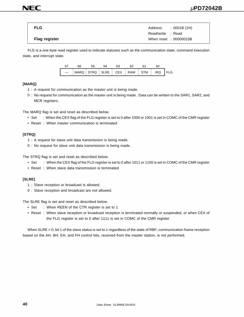
FLG Address : 0001B (1H)
Read/write : Read
Flag register When reset : 00000010B
FLG is a one-byte read register used to indicate statuses such as the communication state, command execution
state, and interrupt state.
b7
—
b6
MARQ
b5
STRQ
b4 b3 b0
RAW FLG
b2 b1
SLRE CEX STM IRQ
[MARQ]
1 : A request for communication as the master unit is being made.
0 : No request for communication as the master unit is being made. Data can be written to the SAR1, SAR2, and
MCR registers.
The MARQ flag is set and reset as described below.
• Set : When the CEX flag of the FLG register is set to 0 after 1000 or 1001 is set in COMC of the CMR register
• Reset : When master communication is terminated
[STRQ]
1 : A request for slave unit data transmission is being made.
0 : No request for slave unit data transmission is being made.
The STRQ flag is set and reset as described below.
• Set : When the CEX flag of the FLG register is set to 0 after 1011 or 1100 is set in COMC of the CMR register
• Reset : When slave data transmission is terminated
[SLRE]
1 : Slave reception or broadcast is allowed.
0 : Slave reception and broadcast are not allowed.
The SLRE flag is set and reset as described below.
• Set : When REEN of the CTR register is set to 1
• Reset : When slave reception or broadcast reception is terminated normally or suspended, or when CEX of
the FLG register is set to 0 after 1111 is set in COMC of the CMR register
When SLRE = 0, bit 1 of the slave status is set to 1 regardless of the state of RBF; communication frame reception
based on the AH, BH, EH, and FH control bits, received from the master station, is not performed.
µPD72042B
41Data Sheet S13990EJ3V0DS
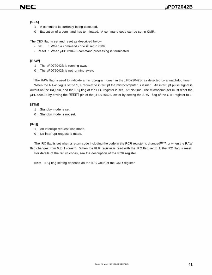
[CEX]
1 : A command is currently being executed.
0 : Execution of a command has terminated. A command code can be set in CMR.
The CEX flag is set and reset as described below.
• Set : When a command code is set in CMR
• Reset : When µPD72042B command processing is terminated
[RAW]
1 : The µPD72042B is running away.
0 : The µPD72042B is not running away.
The RAW flag is used to indicate a microprogram crash in the µPD72042B, as detected by a watchdog timer.
When the RAW flag is set to 1, a request to interrupt the microcomputer is issued. An interrupt pulse signal is
output on the IRQ pin, and the IRQ flag of the FLG register is set. At this time. The microcomputer must reset the
µPD72042B by driving the RESET pin of the µPD72042B low or by setting the SRST flag of the CTR register to 1.
[STM]
1 : Standby mode is set.
0 : Standby mode is not set.
[IRQ]
1 : An interrupt request was made.
0 : No interrupt request is made.
The IRQ flag is set when a return code including the code in the RCR register is changedNote, or when the RAW
flag changes from 0 to 1 (crash). When the FLG register is read with the IRQ flag set to 1, the IRQ flag is reset.
For details of the return codes, see the description of the RCR register.
Note IRQ flag setting depends on the IRS value of the CMR register.
µPD72042B
42 Data Sheet S13990EJ3V0DS
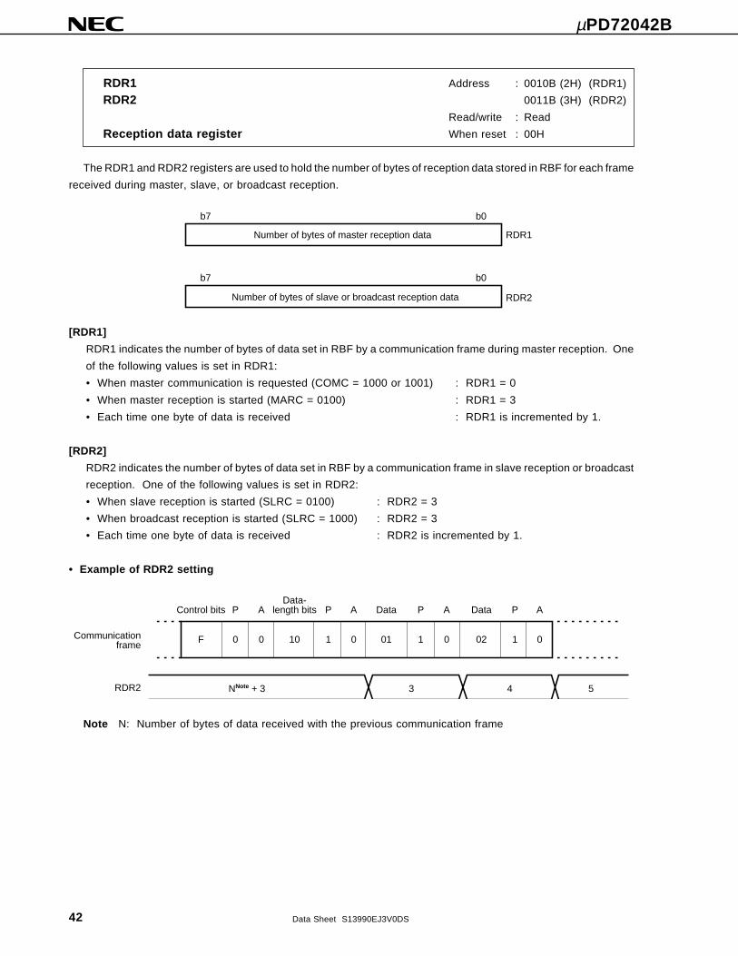
RDR1 Address : 0010B (2H) (RDR1)
RDR2 0011B (3H) (RDR2)
Read/write : Read
Reception data register When reset : 00H
The RDR1 and RDR2 registers are used to hold the number of bytes of reception data stored in RBF for each frame
received during master, slave, or broadcast reception.
b7
Number of bytes of master reception data
b0
RDR1
b7 b0
Number of bytes of slave or broadcast reception data RDR2
[RDR1]
RDR1 indicates the number of bytes of data set in RBF by a communication frame during master reception. One
of the following values is set in RDR1:
• When master communication is requested (COMC = 1000 or 1001) : RDR1 = 0
• When master reception is started (MARC = 0100) : RDR1 = 3
• Each time one byte of data is received : RDR1 is incremented by 1.
[RDR2]
RDR2 indicates the number of bytes of data set in RBF by a communication frame in slave reception or broadcast
reception. One of the following values is set in RDR2:
• When slave reception is started (SLRC = 0100) : RDR2 = 3
• When broadcast reception is started (SLRC = 1000) : RDR2 = 3
• Each time one byte of data is received : RDR2 is incremented by 1.
• Example of RDR2 setting
F 0 0 10 1 0 01 1 0 02 1 0
NNote + 3 3 4 5
Control bits P AData-
length bits P A Data P A Data P A
RDR2
Communicationframe
Note N: Number of bytes of data received with the previous communication frame
µPD72042B
43Data Sheet S13990EJ3V0DS
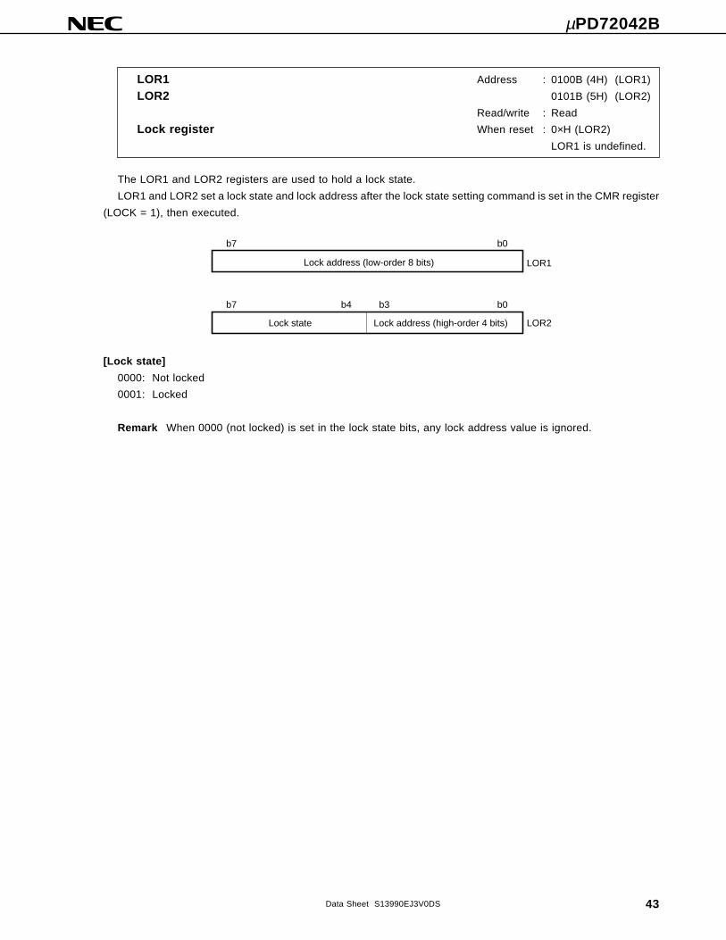
LOR1 Address : 0100B (4H) (LOR1)
LOR2 0101B (5H) (LOR2)
Read/write : Read
Lock register When reset : 0×H (LOR2)
LOR1 is undefined.
The LOR1 and LOR2 registers are used to hold a lock state.
LOR1 and LOR2 set a lock state and lock address after the lock state setting command is set in the CMR register
(LOCK = 1), then executed.
b7
Lock state
b4 b3 b0
Lock address (high-order 4 bits) LOR2
b7 b0
Lock address (low-order 8 bits) LOR1
[Lock state]
0000: Not locked
0001: Locked
Remark When 0000 (not locked) is set in the lock state bits, any lock address value is ignored.
µPD72042B
44 Data Sheet S13990EJ3V0DS
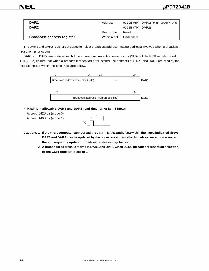
DAR1 Address : 0110B (6H) (DAR1) High-order 4 bits
DAR2 0111B (7H) (DAR2)
Read/write : Read
Broadcast address register When reset : Undefined
The DAR1 and DAR2 registers are used to hold a broadcast address (master address) involved when a broadcast
reception error occurs.
DAR1 and DAR2 are updated each time a broadcast reception error occurs (SLRC of the RCR register is set to
1100). So, ensure that when a broadcast reception error occurs, the contents of DAR1 and DAR2 are read by the
microcomputer within the time indicated below.
b7
Broadcast address (low-order 4 bits)
b4 b3 b0
— DAR1
b7 b0
Broadcast address (high-order 8 bits) DAR2
• Maximum allowable DAR1 and DAR2 read time (t: At fX = 6 MHz):
Approx. 5420 µs (mode 0)
Approx. 1490 µs (mode 1)
Cautions 1. If the microcomputer cannot read the data in DAR1 and DAR2 within the times indicated above,
DAR1 and DAR2 may be updated by the occurrence of another broadcast reception error, and
the subsequently updated broadcast address may be read.
2. A broadcast address is stored in DAR1 and DAR2 when DERC (broadcast reception selection)
of the CMR register is set to 1.
t
IRQ
µPD72042B
45Data Sheet S13990EJ3V0DS
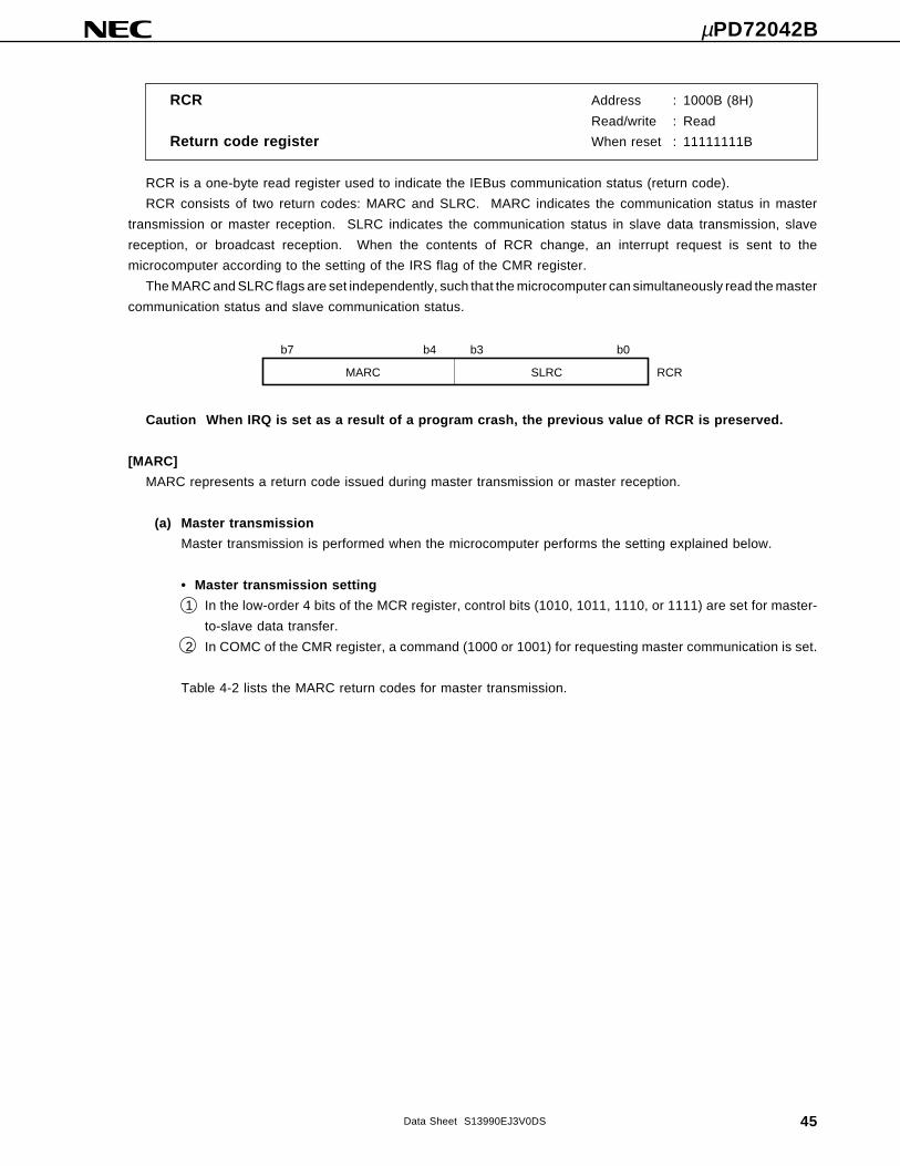
RCR Address : 1000B (8H)
Read/write : Read
Return code register When reset : 11111111B
RCR is a one-byte read register used to indicate the IEBus communication status (return code).
RCR consists of two return codes: MARC and SLRC. MARC indicates the communication status in master
transmission or master reception. SLRC indicates the communication status in slave data transmission, slave
reception, or broadcast reception. When the contents of RCR change, an interrupt request is sent to the
microcomputer according to the setting of the IRS flag of the CMR register.
The MARC and SLRC flags are set independently, such that the microcomputer can simultaneously read the master
communication status and slave communication status.
b7
MARC
b4 b3 b0
SLRC RCR
Caution When IRQ is set as a result of a program crash, the previous value of RCR is preserved.
[MARC]
MARC represents a return code issued during master transmission or master reception.
(a) Master transmission
Master transmission is performed when the microcomputer performs the setting explained below.
• Master transmission setting
1 In the low-order 4 bits of the MCR register, control bits (1010, 1011, 1110, or 1111) are set for master-
to-slave data transfer.
2 In COMC of the CMR register, a command (1000 or 1001) for requesting master communication is set.
Table 4-2 lists the MARC return codes for master transmission.
µPD72042B
46 Data Sheet S13990EJ3V0DS
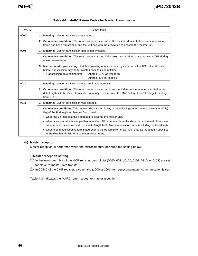
Table 4-2 MARC Return Codes for Master Transmission
MARC Description
0000 1. Meaning: Master transmission is started.
2. Occurrence condition: This return code is issued when the master address field in a communication
frame has been transmitted, and the unit has won the arbitration to become the master unit.
0001 1. Meaning: Master transmission data is not available.
2. Occurrence condition: This return code is issued if the next transmission data is not set in TBF during
master transmission.
3. Microcomputer processing: If data consisting of one or more bytes is not set in TBF within the time
below, transmission may be terminated prior to its completion.
• Transmission data setting time: Approx. 1570 µs (mode 0)
Approx. 390 µs (mode 1)
0010 1. Meaning: Master transmission was terminated normally.
2. Occurrence condition: This return code is issued when as much data as the amount specified in the
data-length field has been transmitted normally. In this case, the MARQ flag of the FLG register changes
from 1 to 0.
0011 1. Meaning: Master transmission was aborted.
2. Occurrence condition: This return code is issued in any of the following cases. In each case, the MARQ
flag of the FLG register changes from 1 to 0.
• When the unit has lost the arbitration to become the master unit.
• When a transmission is stopped because the NAK is returned from the slave unit at the end of the slave
address field, the control field, or the data-length field of a communication frame (excluding the broadcast).
• When a communication is terminated prior to the transmission of as much data as the amount specified
in the data-length field of a communication frame.
(b) Master reception
Master reception is performed when the microcomputer performs the setting below.
• Master reception setting
1 In the low-order 4 bits of the MCR register, control bits (0000, 0011, 0100, 0101, 0110, or 0111) are set
for slave-to-master data transfer.
2 In COMC of the CMR register, a command (1000 or 1001) for requesting master communication is set.
Table 4-3 indicates the MARC return codes for master reception.
µPD72042B
47Data Sheet S13990EJ3V0DS
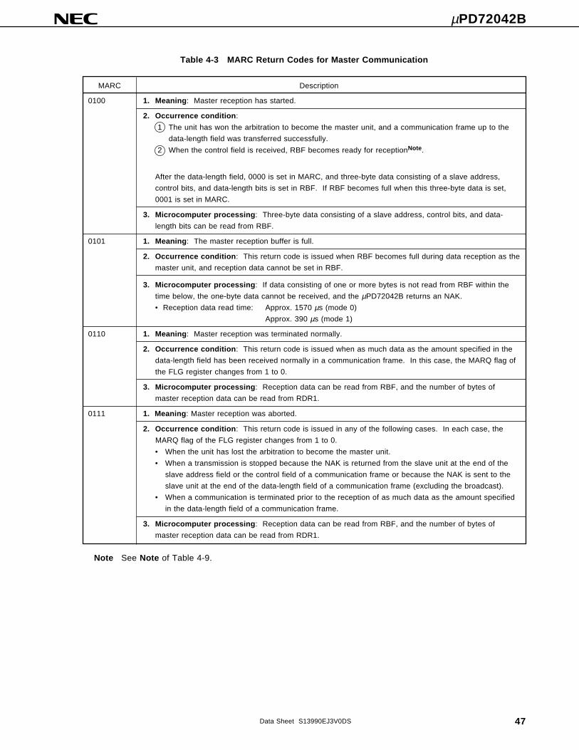
Table 4-3 MARC Return Codes for Master Communication
MARC Description
0100 1. Meaning: Master reception has started.
2. Occurrence condition:
1 The unit has won the arbitration to become the master unit, and a communication frame up to the
data-length field was transferred successfully.
2 When the control field is received, RBF becomes ready for receptionNote.
After the data-length field, 0000 is set in MARC, and three-byte data consisting of a slave address,
control bits, and data-length bits is set in RBF. If RBF becomes full when this three-byte data is set,
0001 is set in MARC.
3. Microcomputer processing: Three-byte data consisting of a slave address, control bits, and data-
length bits can be read from RBF.
0101 1. Meaning: The master reception buffer is full.
2. Occurrence condition: This return code is issued when RBF becomes full during data reception as the
master unit, and reception data cannot be set in RBF.
3. Microcomputer processing: If data consisting of one or more bytes is not read from RBF within the
time below, the one-byte data cannot be received, and the µPD72042B returns an NAK.
• Reception data read time: Approx. 1570 µs (mode 0)
Approx. 390 µs (mode 1)
0110 1. Meaning: Master reception was terminated normally.
2. Occurrence condition: This return code is issued when as much data as the amount specified in the
data-length field has been received normally in a communication frame. In this case, the MARQ flag of
the FLG register changes from 1 to 0.
3. Microcomputer processing: Reception data can be read from RBF, and the number of bytes of
master reception data can be read from RDR1.
0111 1. Meaning: Master reception was aborted.
2. Occurrence condition: This return code is issued in any of the following cases. In each case, the
MARQ flag of the FLG register changes from 1 to 0.
• When the unit has lost the arbitration to become the master unit.
• When a transmission is stopped because the NAK is returned from the slave unit at the end of the
slave address field or the control field of a communication frame or because the NAK is sent to the
slave unit at the end of the data-length field of a communication frame (excluding the broadcast).
• When a communication is terminated prior to the reception of as much data as the amount specified
in the data-length field of a communication frame.
3. Microcomputer processing: Reception data can be read from RBF, and the number of bytes of
master reception data can be read from RDR1.
Note See Note of Table 4-9.
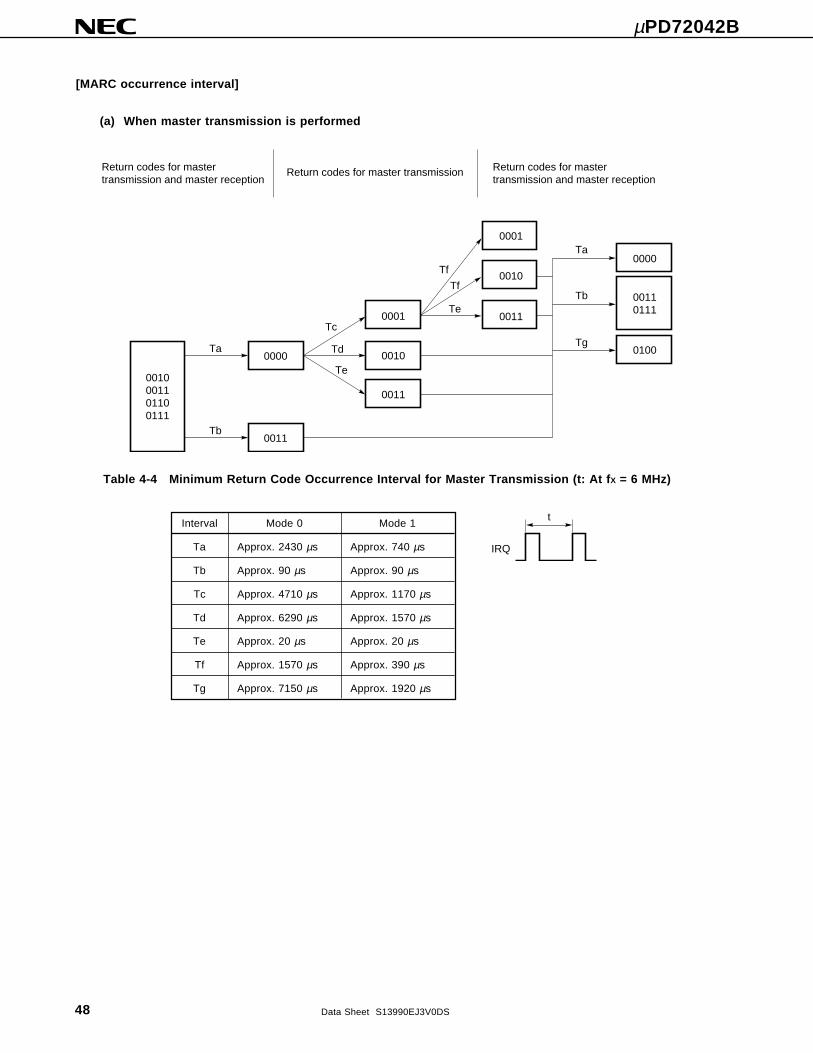
µPD72042B
48 Data Sheet S13990EJ3V0DS
[MARC occurrence interval]
(a) When master transmission is performed
0010001101100111
Ta
Tb
0000
0011
0011
0010
0001Tc
Td
Te
Tf
Tf
Te
Ta
Tb
Tg
0001
0010
0011
0000
00110111
0100
Return codes for master transmission and master reception
Return codes for master transmission and master reception
Return codes for master transmission
Table 4-4 Minimum Return Code Occurrence Interval for Master Transmission (t: At fX = 6 MHz)
Interval Mode 0 Mode 1
Ta Approx. 2430 µs Approx. 740 µs
Tb Approx. 90 µs Approx. 90 µs
Tc Approx. 4710 µs Approx. 1170 µs
Td Approx. 6290 µs Approx. 1570 µs
Te Approx. 20 µs Approx. 20 µs
Tf Approx. 1570 µs Approx. 390 µs
Tg Approx. 7150 µs Approx. 1920 µs
t
IRQ
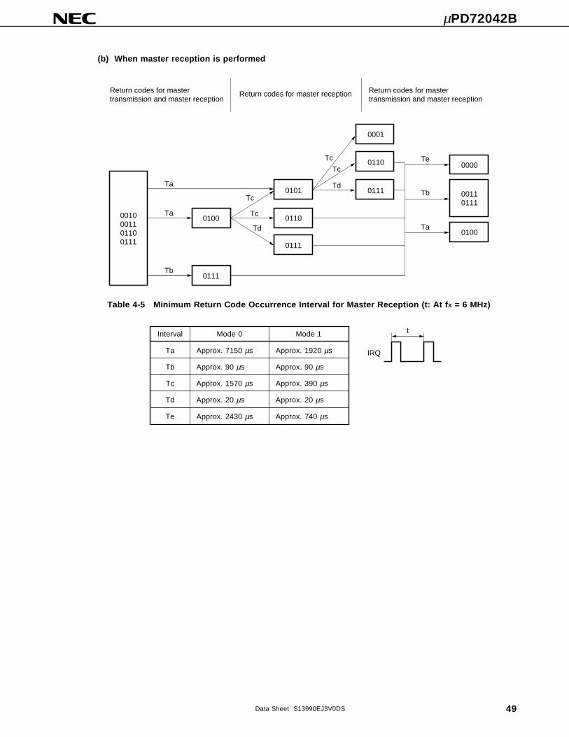
µPD72042B
49Data Sheet S13990EJ3V0DS
(b) When master reception is performed
0010001101100111
Ta
Tb
0100
0111
0111
0110
0101Tc
Tc
Td
Tc
Tc
Td
Te
Tb
Ta
0001
0110
0111
0000
00110111
0100
Ta
Return codes for master transmission and master reception
Return codes for master reception Return codes for master transmission and master reception
Table 4-5 Minimum Return Code Occurrence Interval for Master Reception (t: At fX = 6 MHz)
Interval Mode 0 Mode 1
Ta Approx. 7150 µs Approx. 1920 µs
Tb Approx. 90 µs Approx. 90 µs
Tc Approx. 1570 µs Approx. 390 µs
Td Approx. 20 µs Approx. 20 µs
Te Approx. 2430 µs Approx. 740 µs
t
IRQ
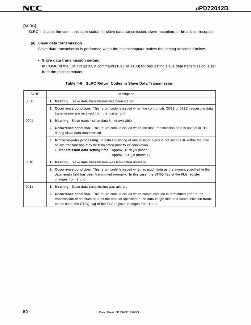
µPD72042B
50 Data Sheet S13990EJ3V0DS
[SLRC]
SLRC indicates the communication status for slave data transmission, slave reception, or broadcast reception.
(a) Slave data transmission
Slave data transmission is performed when the microcomputer makes the setting described below.
• Slave data transmission setting
In COMC of the CMR register, a command (1011 or 1100) for requesting slave data transmission is set
from the microcomputer.
Table 4-6 SLRC Return Codes in Slave Data Transmission
SLRC Description
0000 1. Meaning: Slave data transmission has been started.
2. Occurrence condition: This return code is issued when the control bits (0011 or 0111) requesting data
transmission are received from the master unit.
0001 1. Meaning: Slave transmission data is not available.
2. Occurrence condition: This return code is issued when the next transmission data is not set in TBF
during slave data transmission.
3. Microcomputer processing: If data consisting of one or more bytes is not set in TBF within the time
below, transmission may be terminated prior to its completion.
• Transmission data setting time: Approx. 1570 µs (mode 0)
Approx. 390 µs (mode 1)
0010 1. Meaning: Slave data transmission was terminated normally.
2. Occurrence condition: This return code is issued when as much data as the amount specified in the
data-length field has been transmitted normally. In this case, the STRQ flag of the FLG register
changes from 1 to 0.
0011 1. Meaning: Slave data transmission was aborted.
2. Occurrence condition: This return code is issued when communication is terminated prior to the
transmission of as much data as the amount specified in the data-length field in a communication frame.
In this case, the STRQ flag of the FLG register changes from 1 to 0.
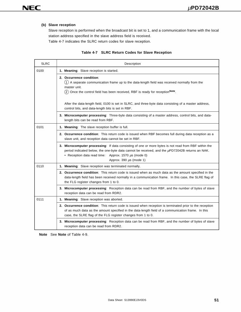
µPD72042B
51Data Sheet S13990EJ3V0DS
(b) Slave reception
Slave reception is performed when the broadcast bit is set to 1, and a communication frame with the local
station address specified in the slave address field is received.
Table 4-7 indicates the SLRC return codes for slave reception.
Table 4-7 SLRC Return Codes for Slave Reception
SLRC Description
0100 1. Meaning: Slave reception is started.
2. Occurrence condition:
1 A separate communication frame up to the data-length field was received normally from the
master unit.
2 Once the control field has been received, RBF is ready for receptionNote.
After the data-length field, 0100 is set in SLRC, and three-byte data consisting of a master address,
control bits, and data-length bits is set in RBF.
3. Microcomputer processing: Three-byte data consisting of a master address, control bits, and data-
length bits can be read from RBF.
0101 1. Meaning: The slave reception buffer is full.
2. Occurrence condition: This return code is issued when RBF becomes full during data reception as a
slave unit, and reception data cannot be set in RBF.
3. Microcomputer processing: If data consisting of one or more bytes is not read from RBF within the
period indicated below, the one-byte data cannot be received, and the µPD72042B returns an NAK.
• Reception data read time: Approx. 1570 µs (mode 0)
Approx. 390 µs (mode 1)
0110 1. Meaning: Slave reception was terminated normally.
2. Occurrence condition: This return code is issued when as much data as the amount specified in the
data-length field has been received normally in a communication frame. In this case, the SLRE flag of
the FLG register changes from 1 to 0.
3. Microcomputer processing: Reception data can be read from RBF, and the number of bytes of slave
reception data can be read from RDR2.
0111 1. Meaning: Slave reception was aborted.
2. Occurrence condition: This return code is issued when reception is terminated prior to the reception
of as much data as the amount specified in the data-length field of a communication frame. In this
case, the SLRE flag of the FLG register changes from 1 to 0.
3. Microcomputer processing: Reception data can be read from RBF, and the number of bytes of slave
reception data can be read from RDR2.
Note See Note of Table 4-9.
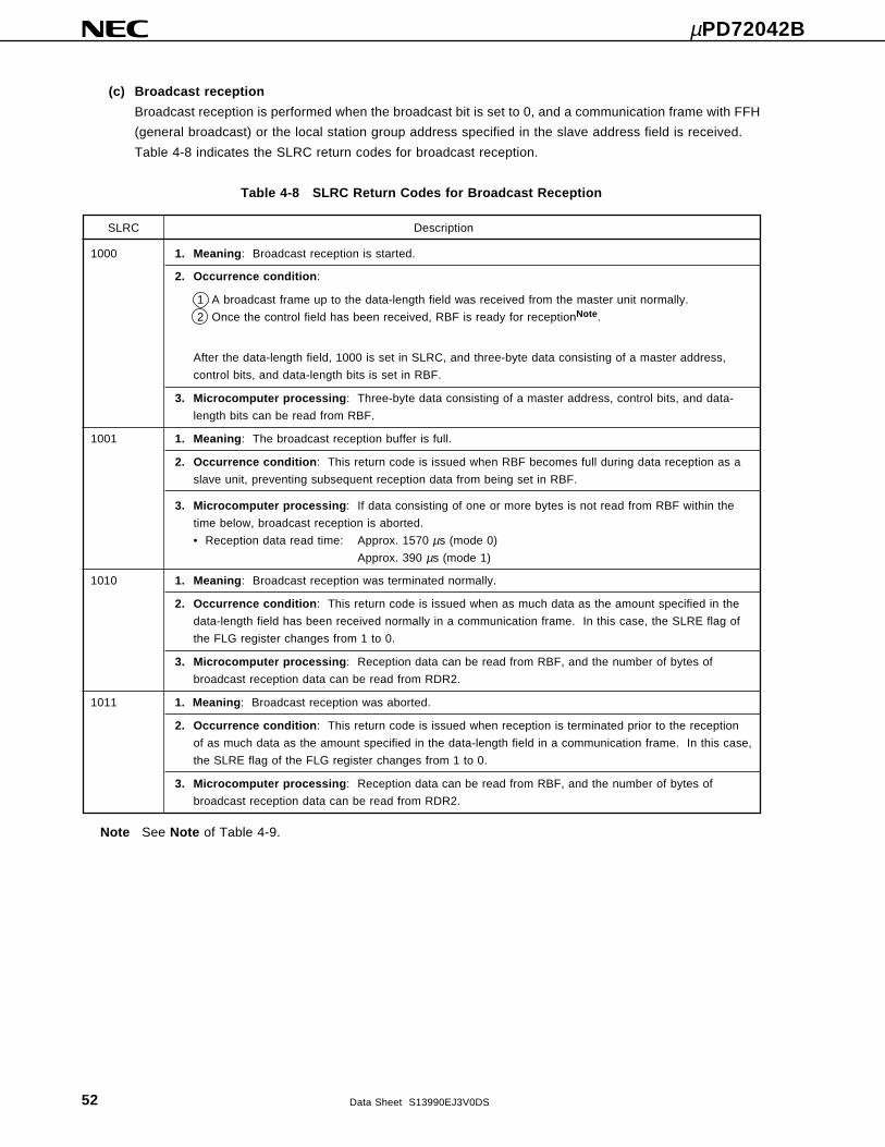
µPD72042B
52 Data Sheet S13990EJ3V0DS
(c) Broadcast reception
Broadcast reception is performed when the broadcast bit is set to 0, and a communication frame with FFH
(general broadcast) or the local station group address specified in the slave address field is received.
Table 4-8 indicates the SLRC return codes for broadcast reception.
Table 4-8 SLRC Return Codes for Broadcast Reception
SLRC Description
1000 1. Meaning: Broadcast reception is started.
2. Occurrence condition:
1 A broadcast frame up to the data-length field was received from the master unit normally.
2 Once the control field has been received, RBF is ready for receptionNote.
After the data-length field, 1000 is set in SLRC, and three-byte data consisting of a master address,
control bits, and data-length bits is set in RBF.
3. Microcomputer processing: Three-byte data consisting of a master address, control bits, and data-
length bits can be read from RBF.
1001 1. Meaning: The broadcast reception buffer is full.
2. Occurrence condition: This return code is issued when RBF becomes full during data reception as a
slave unit, preventing subsequent reception data from being set in RBF.
3. Microcomputer processing: If data consisting of one or more bytes is not read from RBF within the
time below, broadcast reception is aborted.
• Reception data read time: Approx. 1570 µs (mode 0)
Approx. 390 µs (mode 1)
1010 1. Meaning: Broadcast reception was terminated normally.
2. Occurrence condition: This return code is issued when as much data as the amount specified in the
data-length field has been received normally in a communication frame. In this case, the SLRE flag of
the FLG register changes from 1 to 0.
3. Microcomputer processing: Reception data can be read from RBF, and the number of bytes of
broadcast reception data can be read from RDR2.
1011 1. Meaning: Broadcast reception was aborted.
2. Occurrence condition: This return code is issued when reception is terminated prior to the reception
of as much data as the amount specified in the data-length field in a communication frame. In this case,
the SLRE flag of the FLG register changes from 1 to 0.
3. Microcomputer processing: Reception data can be read from RBF, and the number of bytes of
broadcast reception data can be read from RDR2.
Note See Note of Table 4-9.
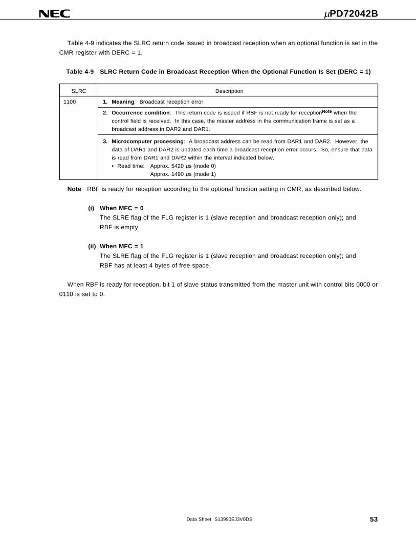
µPD72042B
53Data Sheet S13990EJ3V0DS
Table 4-9 indicates the SLRC return code issued in broadcast reception when an optional function is set in the
CMR register with DERC = 1.
Table 4-9 SLRC Return Code in Broadcast Reception When the Optional Function Is Set (DERC = 1)
SLRC Description
1100 1. Meaning: Broadcast reception error
2. Occurrence condition: This return code is issued if RBF is not ready for receptionNote when the
control field is received. In this case, the master address in the communication frame is set as a
broadcast address in DAR2 and DAR1.
3. Microcomputer processing: A broadcast address can be read from DAR1 and DAR2. However, the
data of DAR1 and DAR2 is updated each time a broadcast reception error occurs. So, ensure that data
is read from DAR1 and DAR2 within the interval indicated below.
• Read time: Approx. 5420 µs (mode 0)
Approx. 1490 µs (mode 1)
Note RBF is ready for reception according to the optional function setting in CMR, as described below.
(i) When MFC = 0
The SLRE flag of the FLG register is 1 (slave reception and broadcast reception only); and
RBF is empty.
(ii) When MFC = 1
The SLRE flag of the FLG register is 1 (slave reception and broadcast reception only); and
RBF has at least 4 bytes of free space.
When RBF is ready for reception, bit 1 of slave status transmitted from the master unit with control bits 0000 or
0110 is set to 0.
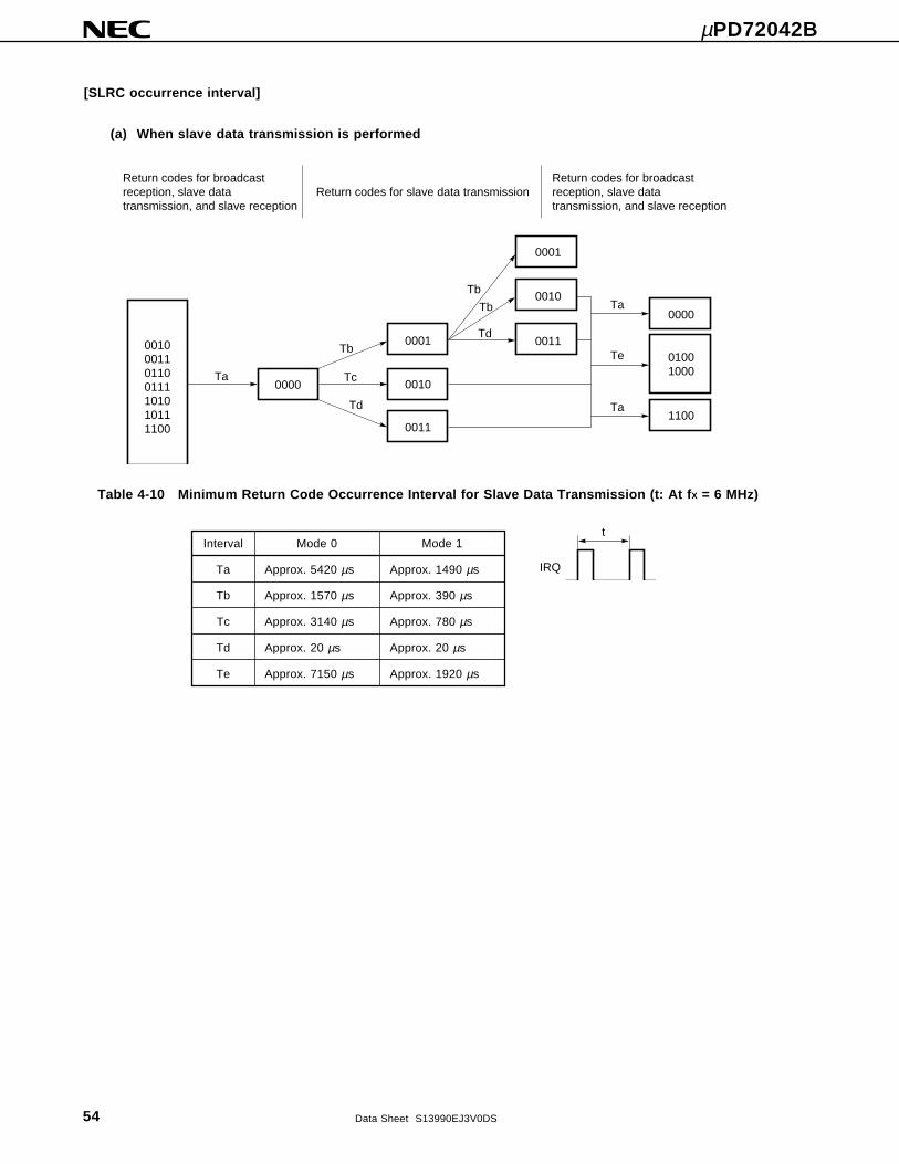
µPD72042B
54 Data Sheet S13990EJ3V0DS
[SLRC occurrence interval]
(a) When slave data transmission is performed
0010001101100111101010111100
Ta0000
0011
0010
0001Tb
Tc
Td
Tb
Tb
Td
Ta
Te
Ta
0001
0010
0011
0000
01001000
1100
Return codes for broadcast reception, slave data transmission, and slave reception
Return codes for slave data transmissionReturn codes for broadcast reception, slave data transmission, and slave reception
Table 4-10 Minimum Return Code Occurrence Interval for Slave Data Transmission (t: At fX = 6 MHz)
Interval Mode 0 Mode 1
Ta Approx. 5420 µs Approx. 1490 µs
Tb Approx. 1570 µs Approx. 390 µs
Tc Approx. 3140 µs Approx. 780 µs
Td Approx. 20 µs Approx. 20 µs
Te Approx. 7150 µs Approx. 1920 µs
t
IRQ
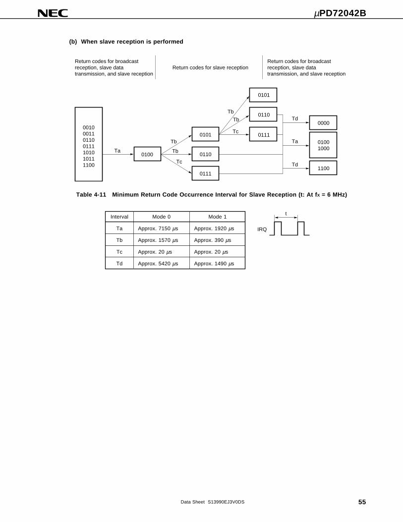
µPD72042B
55Data Sheet S13990EJ3V0DS
(b) When slave reception is performed
0010001101100111101010111100
Ta0100
0111
0110
0101Tb
Tb
Tc
Tb
Tb
Tc
Td
Ta
Td
0101
0110
0111
0000
01001000
1100
Return codes for broadcast reception, slave data transmission, and slave reception
Return codes for slave receptionReturn codes for broadcast reception, slave data transmission, and slave reception
Table 4-11 Minimum Return Code Occurrence Interval for Slave Reception (t: At fX = 6 MHz)
Interval Mode 0 Mode 1
Ta Approx. 7150 µs Approx. 1920 µs
Tb Approx. 1570 µs Approx. 390 µs
Tc Approx. 20 µs Approx. 20 µs
Td Approx. 5420 µs Approx. 1490 µs
t
IRQ
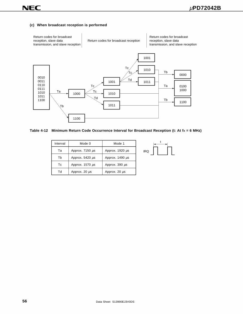
µPD72042B
56 Data Sheet S13990EJ3V0DS
(c) When broadcast reception is performed
0010001101100111101010111100
Ta1000
1011
1010
1001Tc
Tc
Td
Tc
Tc
Td
Tb
Ta
Tb
1001
1010
1011
0000
01001000
1100Tb
1100
Return codes for broadcast reception, slave data transmission, and slave reception
Return codes for broadcast receptionReturn codes for broadcast reception, slave data transmission, and slave reception
Table 4-12 Minimum Return Code Occurrence Interval for Broadcast Reception (t: At fX = 6 MHz)
Interval Mode 0 Mode 1
Ta Approx. 7150 µs Approx. 1920 µs
Tb Approx. 5420 µs Approx. 1490 µs
Tc Approx. 1570 µs Approx. 390 µs
Td Approx. 20 µs Approx. 20 µs
t
IRQ

µPD72042B
57Data Sheet S13990EJ3V0DS
RBF Address : 1110B (EH)
Read/write : Read
Reception buffer When reset : Undefined
RBF is a 40-byte FIFO buffer used to hold a transmitter address, control bits, data-length bits, and reception data
for master reception, slave reception, or broadcast reception.
RBF can be read by the microcomputer when the REP flag of the STR register is 0 (indicating that RBF is not empty).
When an optional function is set in the CMR register with MFC = 1, multiple communication frames can be held
in RBF until RBF becomes full.
In master reception, slave reception, and broadcast reception, the format below is used to transfer data from RBF
to the microcomputer.
RBF
High-order 4 bits Low-order 4 bits
Byte 2
Byte 1
Byte 3
Byte 4
Byte 5
Byte 40
Transmitter address (high-order 8 bits)
Transmitter address (low-order 4 bits) Control bits
Data-length bits
First byte of reception data
Second byte of reception data
Last reception data
Transmitter address (high-order 8 bits)
Transmitter address (low-order 4 bits) Control bits
Data-length bits
First byte of reception data
Second byte of reception data
Last reception data
Communication frame 1
Communication frame 2
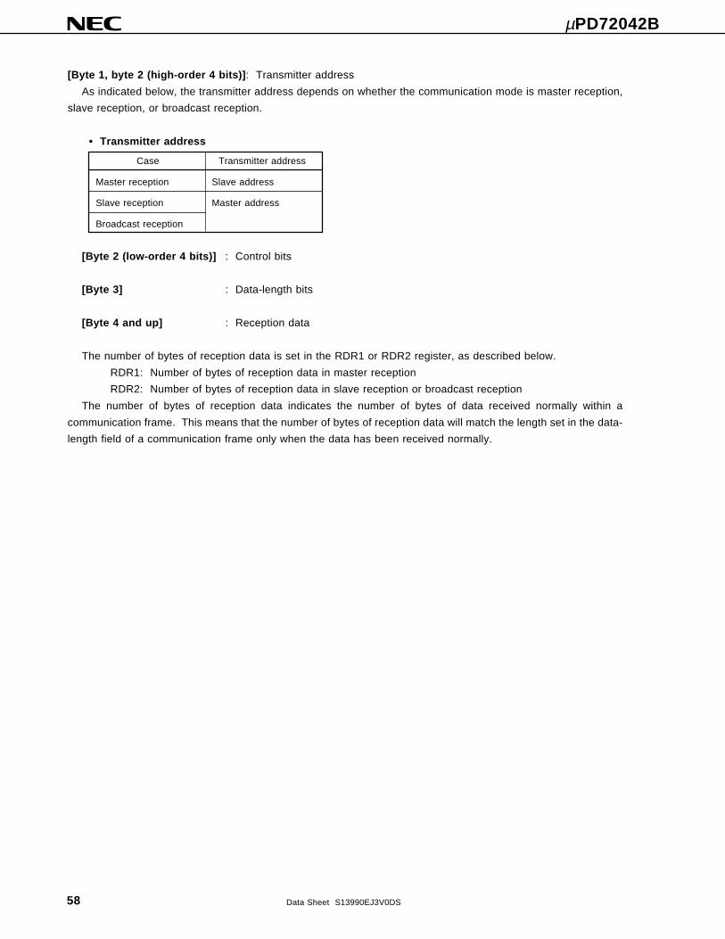
µPD72042B
58 Data Sheet S13990EJ3V0DS
[Byte 1, byte 2 (high-order 4 bits)]: Transmitter address
As indicated below, the transmitter address depends on whether the communication mode is master reception,
slave reception, or broadcast reception.
• Transmitter address
Case Transmitter address
Master reception Slave address
Slave reception Master address
Broadcast reception
[Byte 2 (low-order 4 bits)] : Control bits
[Byte 3] : Data-length bits
[Byte 4 and up] : Reception data
The number of bytes of reception data is set in the RDR1 or RDR2 register, as described below.
RDR1: Number of bytes of reception data in master reception
RDR2: Number of bytes of reception data in slave reception or broadcast reception
The number of bytes of reception data indicates the number of bytes of data received normally within a
communication frame. This means that the number of bytes of reception data will match the length set in the data-
length field of a communication frame only when the data has been received normally.
µPD72042B
59Data Sheet S13990EJ3V0DS
5. EXAMPLE TIMINGS FOR COMMUNICATION
This chapter provides examples of the timings at which the contents of internal registers change during
communication. The following seven examples are given:
(1) Master transmission timing example 1
Timing at which a return code is generated upon the start of master transmission and at the normal termination
of transmission
(2) Master transmission timing example 2
Timing at which a return code is generated upon the start of master transmission, transmission data empty, and
the suspension of transmission
(3) Slave data transmission timing example
Timing at which a return code is generated upon the start of slave data transmission and the normal termination
of transmission
(4) Master reception timing example
Timing at which a return code is generated upon the start of master reception and the normal termination of
reception
(5) Slave reception timing example 1
Timing at which a return code is generated upon the start of slave reception and the normal termination of
reception
(6) Slave reception timing example 2
Timing at which a return code is generated upon the start of slave reception, reception buffer full, and the normal
termination of reception
(7) Broadcast reception timing example
Timing at which a return code is generated upon the occurrence of an error during broadcast reception
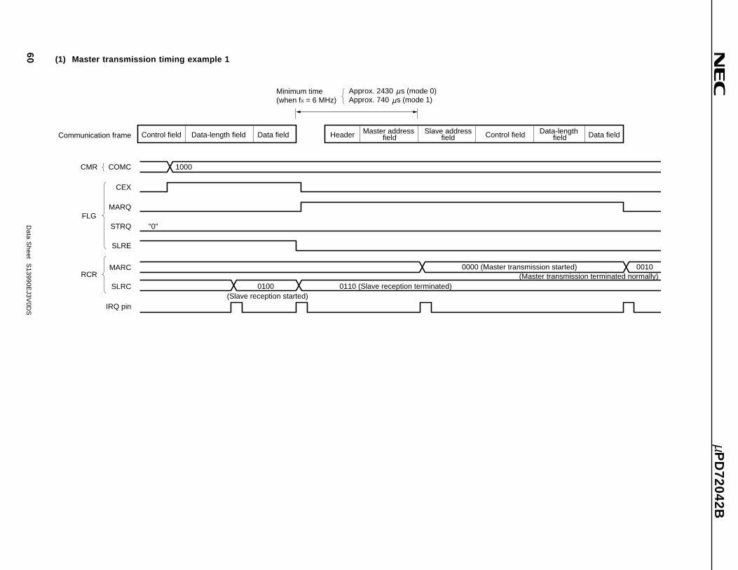
µP
D72042B
60D
ata Sheet S
13990EJ3V
0DS
(1) Master transmission timing example 1
CMR
FLG
COMC
CEX
MARQ
STRQ
SLRE
MARC
SLRC
"0"
1000
0100
IRQ pin
Minimum time (when fX = 6 MHz)
Approx. 2430 s (mode 0)Approx. 740 s (mode 1)
Communication frame Control field Data-length field Data field Header Master address field Control field Data field
0000 (Master transmission started) 0010(Master transmission terminated normally)
0110 (Slave reception terminated)(Slave reception started)
RCR
Slave addressfield
Data-length field
µµ
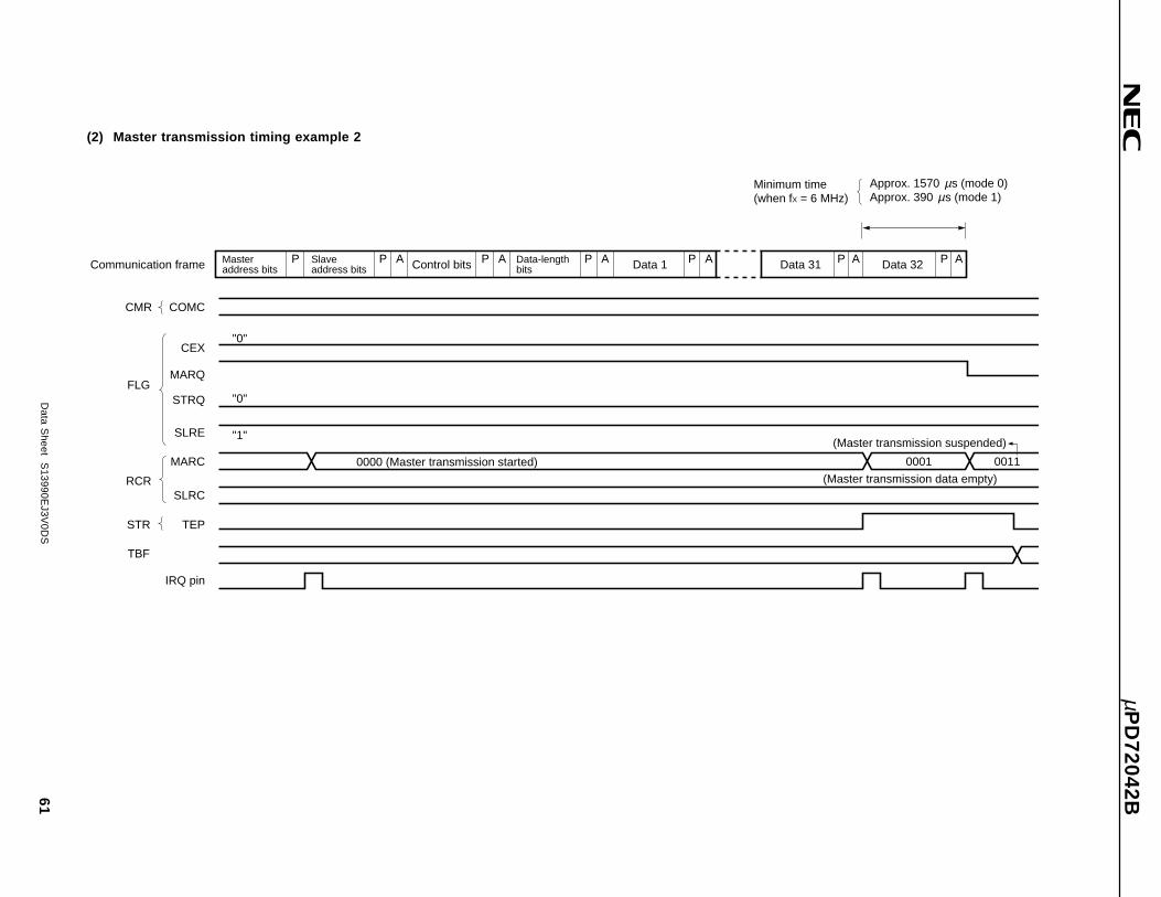
µP
D72042B61
Data S
heet S13990E
J3V0D
S
(2) Master transmission timing example 2
CMR
FLG
COMC
CEX
MARQ
STRQ
SLRE
MARC
SLRC
"0"
IRQ pin
"0"
"1"
TEP
RCR
STR
TBF
Communication frame
Minimum time (when fX = 6 MHz)
Master address bits
Slaveaddress bits Control bits Data-length
bitsP P A P A P A P A P A P AData 1 Data 31 Data 32
0000 (Master transmission started)
(Master transmission suspended)
00110001
(Master transmission data empty)
Approx. 1570 s (mode 0)Approx. 390 s (mode 1)
µµ
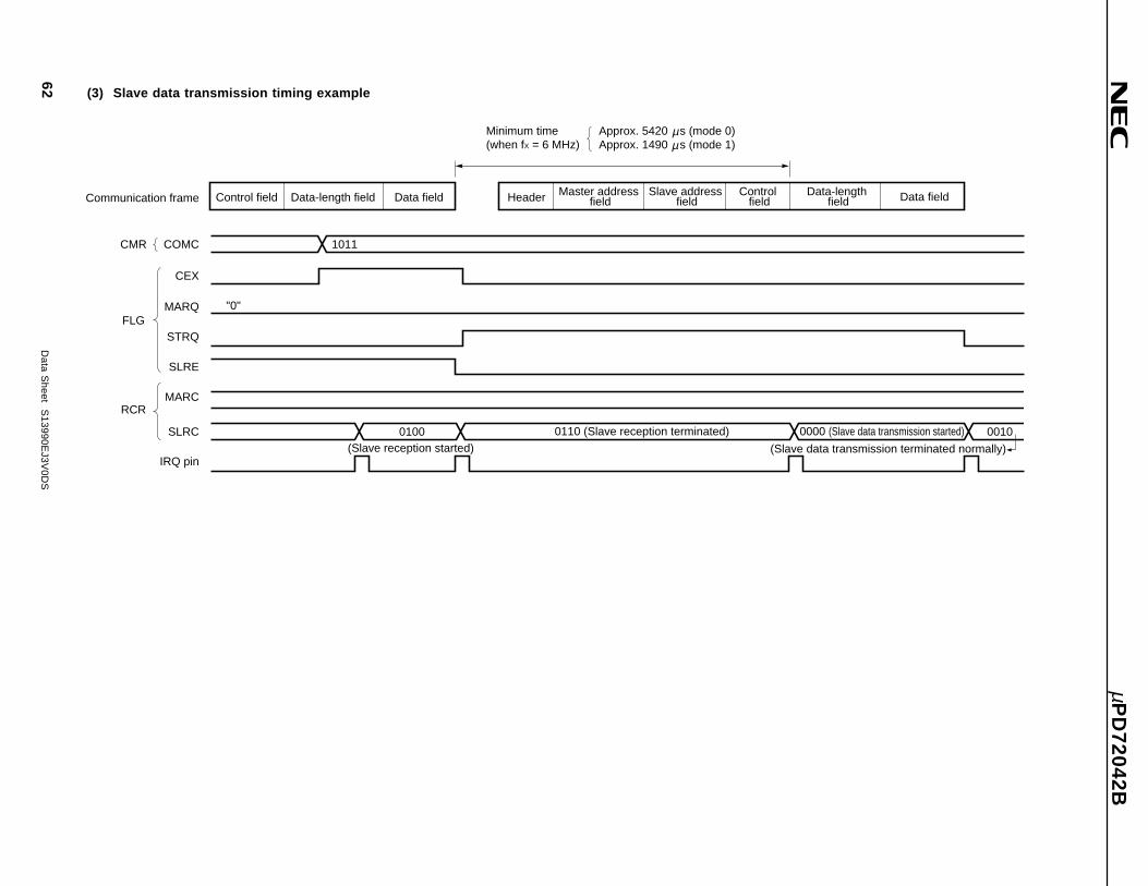
µP
D72042B
62D
ata Sheet S
13990EJ3V
0DS
(3) Slave data transmission timing example
CMR
FLG
COMC
CEX
MARQ
STRQ
SLRE
MARC
SLRC
"0"
1011
0100
IRQ pin
RCR
Minimum time (when fX = 6 MHz)
Approx. 5420 s (mode 0)Approx. 1490 s (mode 1)
Communication frame Control field Data-length field Data field Header Slave address field Data field
(Slave reception started)0110 (Slave reception terminated) 0000 (Slave data transmission started) 0010
(Slave data transmission terminated normally)
µµ
Master address field
Control field
Data-length field
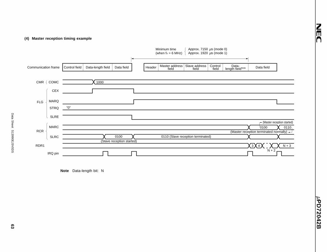
µP
D72042B63
Data S
heet S13990E
J3V0D
S
(4) Master reception timing example
Note Data-length bit: N
CMR
FLG
COMC
CEX
MARQ
STRQ
SLRE
MARC
SLRC
"0"
IRQ pin
RCR
RDR1
Communication frame
Minimum time (when fX = 6 MHz)
Approx. 7150 s (mode 0)Approx. 1920 s (mode 1)
Control field Data-length field Data field Header Master addressfield Data field
(Master reception started)
0100 0110(Master reception terminated normally)
(Slave reception started)0100 0110 (Slave reception terminated)
3 4 N + 3N + 2
1000
µµ
Slave addressfield
Control field
Data-length fieldNote

µP
D72042B
64D
ata Sheet S
13990EJ3V
0DS
(5) Slave reception timing example 1
CTR
FLG
REEN
CEX
MARQ
STRQ
SLRE
MARC
SLRC
IRQ pin
RCR
RDR2
Communication frame
"0"
"0"
"0"
Minimum time (when fX = 6 MHz)
Approx. 5260 s (mode 0)Approx. 1450 s (mode 1)
Control field Data-length field Data field Header Master address field Data field
Separate frame (data-length bits: N1) Broadcast frame (data-length bits: N2)
1000(Broadcast reception started)
3 4 N1 + 3
N1 + 2
1010 (Broadcast reception terminated normally)(Slave reception started)
0100 0110(Slave reception terminated normally)
3 4 N2 + 3N2 + 2
Slave address field
Control field
Data-length field
µµ
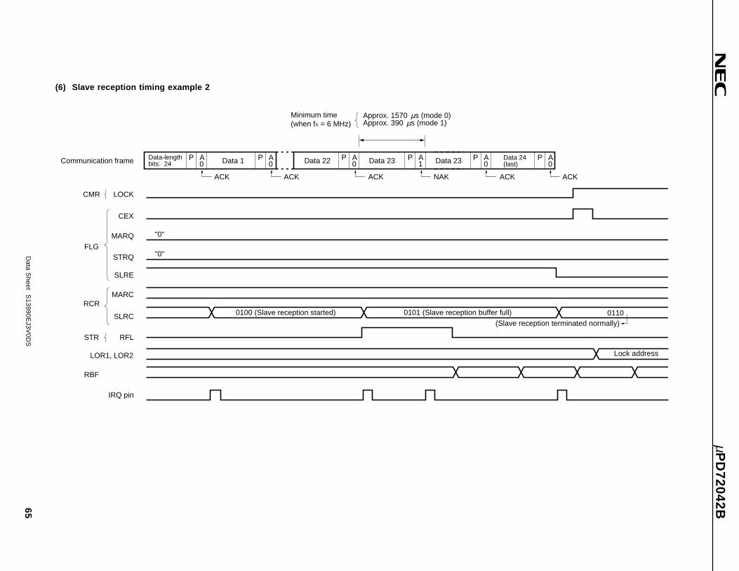
µP
D72042B65
Data S
heet S13990E
J3V0D
S
(6) Slave reception timing example 2
CMR
FLG
LOCK
CEX
MARQ
STRQ
SLRE
MARC
SLRC
"0"
IRQ pin
RFL
RCR
STR
LOR1, LOR2
Communication frame
RBF
"0"
Minimum time (when fX = 6 MHz)
Data-length bits: 24
P A0 Data 1 P A
0 Data 22 P A0 Data 23 P A
1P A
0Data 23 P A0
Data 24 (last)
0100 (Slave reception started) 0101 (Slave reception buffer full) 0110(Slave reception terminated normally)
ACK ACK ACK NAK ACK ACK
Lock address
Approx. 1570 s (mode 0)Approx. 390 s (mode 1)
µµ
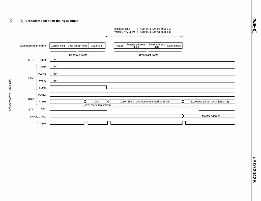
µP
D72042B
66D
ata Sheet S
13990EJ3V
0DS
(7) Broadcast reception timing example
CTR
FLG
REEN
CEX
MARQ
STRQ
SLRE
MARC
SLRC
"0"
IRQ pin
RFL
RCR
STR
DAR1, DAR2
Communication frame
"0"
"0"
"0"
Minimum time (when fX = 6 MHz)
Approx. 5420 s (mode 0)Approx. 1490 s (mode 1)
Control field Data-length field Data field Header Master address field Control field
Broadcast frameSeparate frame
0100(Slave reception started)
0110 (Slave reception terminated normally) 1100 (Broadcast reception error)
Master address
Slave address field
µµ
µPD72042B
67Data Sheet S13990EJ3V0DS
6. EXAMPLE MICROCOMPUTER PROCESSING FLOW
This chapter provides an example of the processing flow for controlling the µPD72042B from the microcomputer.
The main parts of this example processing flow are the following two routines:
• Main routine
Performs processing based on the communication flags set by the interrupt routine.
• Interrupt routine
Sets the communication flags by reading the statuses of the µPD72042B upon the issue of an interrupt request.
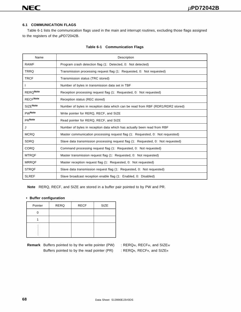
µPD72042B
68 Data Sheet S13990EJ3V0DS
Name Description
RAWF Program crash detection flag (1: Detected, 0: Not detected)
TRRQ Transmission processing request flag (1: Requested, 0: Not requested)
TRCF Transmission status (TRC stored)
I Number of bytes in transmission data set in TBF
RERQNote Reception processing request flag (1: Requested, 0: Not requested)
RECFNote Reception status (REC stored)
SIZENote Number of bytes in reception data which can be read from RBF (RDR1/RDR2 stored)
PWNote Write pointer for RERQ, RECF, and SIZE
PRNote Read pointer for RERQ, RECF, and SIZE
J Number of bytes in reception data which has actually been read from RBF
MCRQ Master communication processing request flag (1: Requested, 0: Not requested)
SDRQ Slave data transmission processing request flag (1: Requested, 0: Not requested)
CORQ Command processing request flag (1: Requested, 0: Not requested)
MTRQF Master transmission request flag (1: Requested, 0: Not requested)
MRRQF Master reception request flag (1: Requested, 0: Not requested)
STRQF Slave data transmission request flag (1: Requested, 0: Not requested)
SLREF Slave broadcast reception enable flag (1: Enabled, 0: Disabled)
Pointer RERQ RECF SIZE
0
1
....
....
....
6.1 COMMUNICATION FLAGS
Table 6-1 lists the communication flags used in the main and interrupt routines, excluding those flags assigned
to the registers of the µPD72042B.
Table 6-1 Communication Flags
Note RERQ, RECF, and SIZE are stored in a buffer pair pointed to by PW and PR.
• Buffer configuration
Remark Buffers pointed to by the write pointer (PW) : RERQW, RECFW, and SIZEW
Buffers pointed to by the read pointer (PR) : RERQR, RECFR, and SIZER
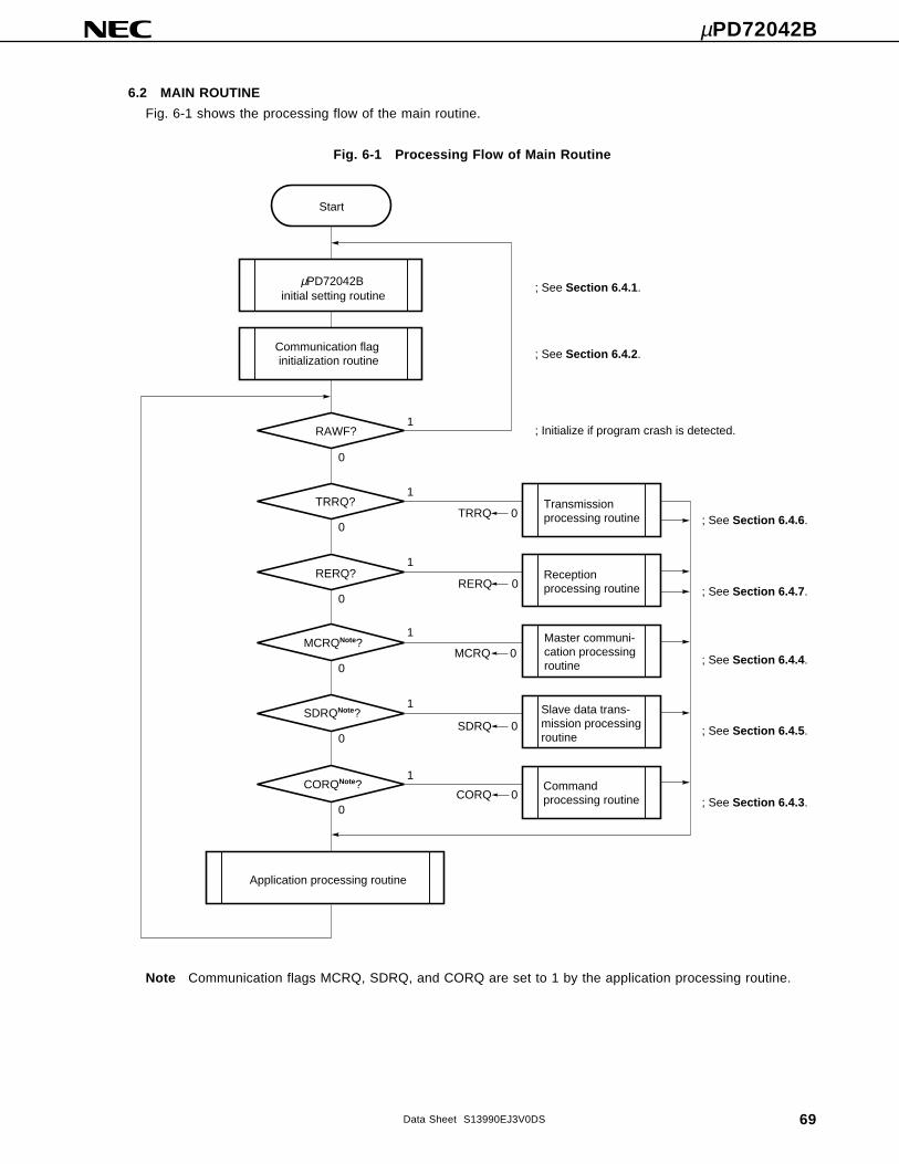
µPD72042B
69Data Sheet S13990EJ3V0DS
6.2 MAIN ROUTINE
Fig. 6-1 shows the processing flow of the main routine.
Fig. 6-1 Processing Flow of Main Routine
Note Communication flags MCRQ, SDRQ, and CORQ are set to 1 by the application processing routine.
Start
; See Section 6.4.1.initial setting routine
Communication flag initialization routine ; See Section 6.4.2.
; Initialize if program crash is detected.
Transmission processing routine
Reception processing routine
Master communi-cation processing routine
Slave data trans-mission processing routine
Command processing routine
; See Section 6.4.6.
; See Section 6.4.7.
; See Section 6.4.4.
; See Section 6.4.5.
; See Section 6.4.3.
Application processing routine
RAWF?
TRRQ?
0
0
RERQ?
0
MCRQNote?
0
SDRQNote?
0
CORQNote?
0
1
1
1
1
1
1
TRRQ 0
RERQ 0
MCRQ 0
SDRQ 0
CORQ 0
µPD72042B
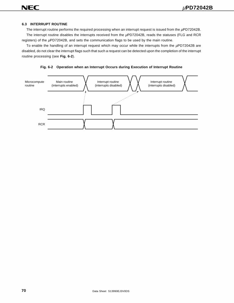
µPD72042B
70 Data Sheet S13990EJ3V0DS
6.3 INTERRUPT ROUTINE
The interrupt routine performs the required processing when an interrupt request is issued from the µPD72042B.
The interrupt routine disables the interrupts received from the µPD72042B, reads the statuses (FLG and RCR
registers) of the µPD72042B, and sets the communication flags to be used by the main routine.
To enable the handling of an interrupt request which may occur while the interrupts from the µPD72042B are
disabled, do not clear the interrupt flags such that such a request can be detected upon the completion of the interrupt
routine processing (see Fig. 6-2).
Fig. 6-2 Operation when an Interrupt Occurs during Execution of Interrupt Routine
IRQ
RCR
Microcomputeroutine
Main routine (interrupts enabled)
Interrupt routine (interrupts disabled)
Interrupt routine (interrupts disabled)
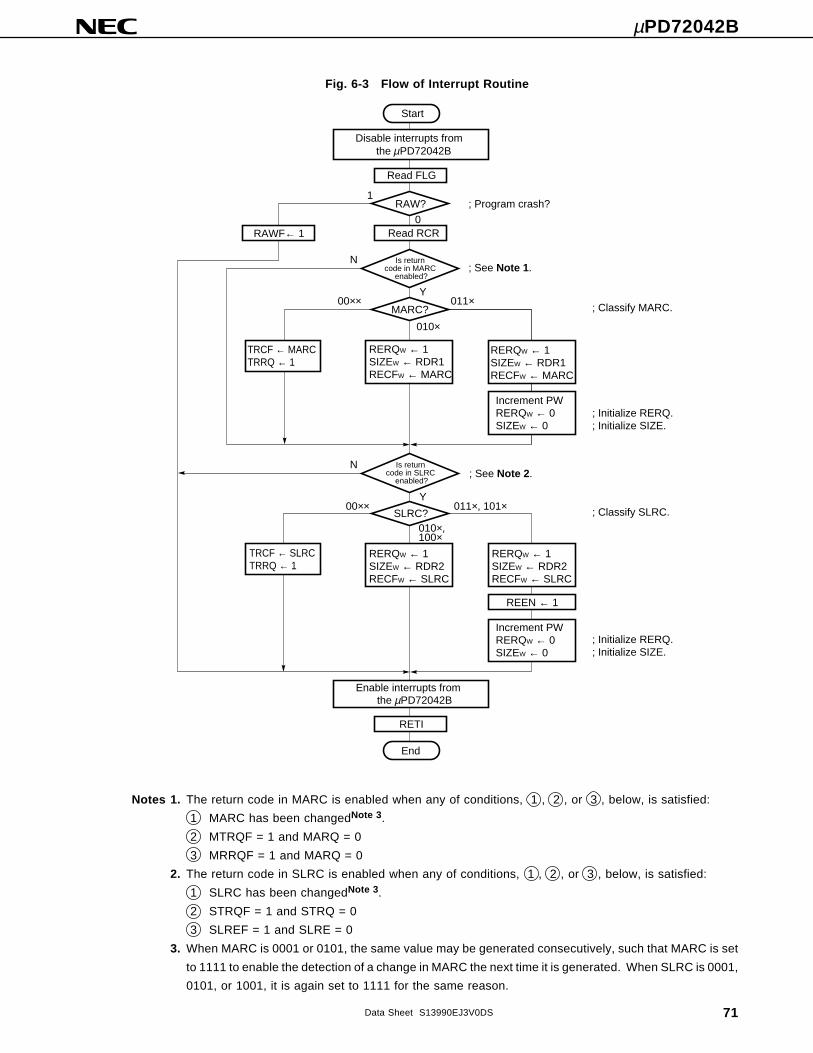
µPD72042B
71Data Sheet S13990EJ3V0DS
Fig. 6-3 Flow of Interrupt Routine
Notes 1. The return code in MARC is enabled when any of conditions, 1 , 2 , or 3 , below, is satisfied:
1 MARC has been changedNote 3.
2 MTRQF = 1 and MARQ = 0
3 MRRQF = 1 and MARQ = 0
2. The return code in SLRC is enabled when any of conditions, 1 , 2 , or 3 , below, is satisfied:
1 SLRC has been changedNote 3.
2 STRQF = 1 and STRQ = 0
3 SLREF = 1 and SLRE = 0
3. When MARC is 0001 or 0101, the same value may be generated consecutively, such that MARC is set
to 1111 to enable the detection of a change in MARC the next time it is generated. When SLRC is 0001,
0101, or 1001, it is again set to 1111 for the same reason.
Start
Disable interrupts from
Read FLG
RAW?1
0
; Program crash?
Read RCR
; See Note 1.Is return
code in MARC enabled?
MARC?011×00××
010×
; Classify MARC.
RERQW ← 1SIZEW ← RDR1RECFW ← MARC
Is return code in SLRC
enabled?
N
RERQW ← 1SIZEW ← RDR2RECFW ← SLRC
SLRC?
Y
010×,100×
011×, 101×00××
TRCF ← SLRCTRRQ ← 1
Enable interrupts from
End
RETI
; Initialize RERQ.; Initialize SIZE.
; Classify SLRC.
; See Note 2.
; Initialize RERQ.; Initialize SIZE.
RAWF← 1
TRCF ← MARCTRRQ ← 1
Increment PWRERQW ← 0SIZEW ← 0
RERQW ← 1SIZEW ← RDR1RECFW ← MARC
RERQW ← 1SIZEW ← RDR2RECFW ← SLRC
REEN ← 1
Increment PWRERQW ← 0SIZEW ← 0
µthe PD72042B
N
Y
µthe PD72042B
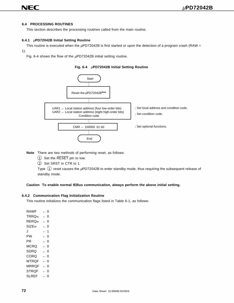
µPD72042B
72 Data Sheet S13990EJ3V0DS
6.4 PROCESSING ROUTINES
This section describes the processing routines called from the main routine.
6.4.1 µPD72042B Initial Setting Routine
This routine is executed when the µPD72042B is first started or upon the detection of a program crash (RAW =
1).
Fig. 6-4 shows the flow of the µPD72042B initial setting routine.
Fig. 6-4 µPD72042B Initial Setting Routine
Note There are two methods of performing reset, as follows:
1 Set the RESET pin to low.
2 Set SRST in CTR to 1.
Type 1 reset causes the µPD72042B to enter standby mode, thus requiring the subsequent release of
standby mode.
Caution To enable normal IEBus communication, always perform the above initial setting.
6.4.2 Communication Flag Initialization Routine
This routine initializes the communication flags listed in Table 6-1, as follows:
RAWF ← 0TRRQW ← 0RERQW ← 0
SIZEW ← 0J ← 1PW ← 0
PR ← 0MCRQ ← 0SDRQ ← 0
CORQ ← 0MTRQF ← 0MRRQF ← 0
STRQF ← 0SLREF ← 0
Start
Reset the PD72042BNote
UAR1 ← Local station address (four low-order bits)UAR2 ← Local station address (eight high-order bits)
End
CMR ← 100000 b1 b0
; Set local address and condition code.
; Set condition code.
; Set optional functions.
µ
Condition code
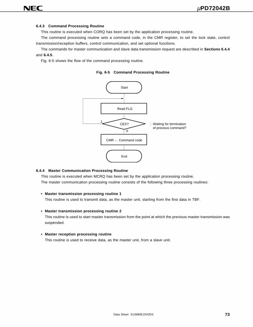
µPD72042B
73Data Sheet S13990EJ3V0DS
6.4.3 Command Processing Routine
This routine is executed when CORQ has been set by the application processing routine.
The command processing routine sets a command code, in the CMR register, to set the lock state, control
transmission/reception buffers, control communication, and set optional functions.
The commands for master communication and slave data transmission request are described in Sections 6.4.4
and 6.4.5.
Fig. 6-5 shows the flow of the command processing routine.
Fig. 6-5 Command Processing Routine
Start
Read FLG
CMR ← Command code
End
;CEX?
0
1Waiting for termination of previous command?
6.4.4 Master Communication Processing Routine
This routine is executed when MCRQ has been set by the application processing routine.
The master communication processing routine consists of the following three processing routines:
• Master transmission processing routine 1
This routine is used to transmit data, as the master unit, starting from the first data in TBF.
• Master transmission processing routine 2
This routine is used to start master transmission from the point at which the previous master transmission was
suspended.
• Master reception processing routine
This routine is used to receive data, as the master unit, from a slave unit.

µPD72042B
74 Data Sheet S13990EJ3V0DS
(1) Master transmission processing routine 1
Fig. 6-6 shows the flow of master transmission processing routine 1.
Fig. 6-6 Flow of Master Transmission Processing Routine 1
Start
SAR1 ← Slave address (four low-order bits)SAR2 ← Slave address (eight high-order bits)MCR ← Broadcast bits, number of arbitrations, and control bits (The MSB is 1.)
Read STR
TEP?1
0
Read FLG
CEX?
0
1
CMR ← 00010000
Read FLG
CEX?
0
1
TBF ← Number of bytes in transmission data
I ← 1
I >
N
Y
Read STR
TFL?1
0
I ← I + 1
TBF ← Transmission data (I-th byte)
1
Read FLG
CEX?
0
End
CMR← 00001000
MTRQF← 1
; Waiting for termination of previous command?
; Set clear command for transmission buffer.
; Waiting for termination of processing of transmission buffer clear command?
; Initialize I.
; Setting tranmission data in TBF completed?
;
; Waiting for termination of processing of master communication request command?
Number of bytes in tranmission data
Set master communication request command.
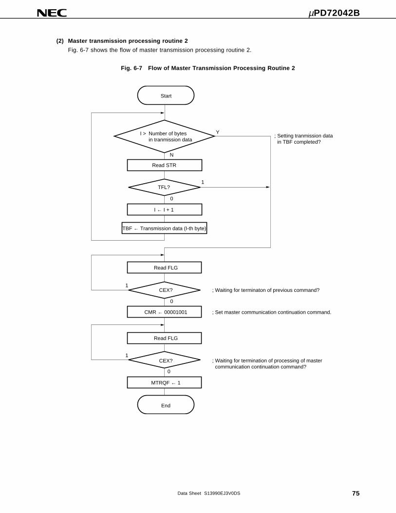
µPD72042B
75Data Sheet S13990EJ3V0DS
(2) Master transmission processing routine 2
Fig. 6-7 shows the flow of master transmission processing routine 2.
Fig. 6-7 Flow of Master Transmission Processing Routine 2
Start
I > Y
N
Read STR
TFL?1
0
TBF ← Transmission data (I-th byte)
I ← I + 1
Read FLG
CEX?
CMR ← 00001001
Read FLG
CEX?
0
MTRQF ← 1
End
1
1; Waiting for terminaton of previous command?
; Set master communication continuation command.
;
;
Waiting for termination of processing of master communication continuation command?
Number of bytes in tranmission data
0
Setting tranmission data in TBF completed?
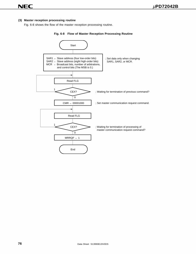
µPD72042B
76 Data Sheet S13990EJ3V0DS
(3) Master reception processing routine
Fig. 6-8 shows the flow of the master reception processing routine.
Fig. 6-8 Flow of Master Reception Processing Routine
Start
SAR1 ← Slave address (four low-order bits)SAR2 ← Slave address (eight high-order bits)MCR ← Broadcast bits, number of arbitrations, and control bits (The MSB is 0.)
Read FLG
CEX?1
0
CMR ← 00001000
Read FLG
CEX?
End
MRRQF ← 1
;
; Set master communication request command.
; Waiting for termination of previous command?
;
1
0
Set data only when changing SAR1, SAR2, or MCR.
Waiting for termination of processing of master communication request command?
µPD72042B
77Data Sheet S13990EJ3V0DS
6.4.5 Slave Data Transmission Processing Routine
This routine is executed when SDRQ has been set by the application processing routine.
The slave data transmission processing routine consists of the following two processing routines:
• Slave data transmission processing routine 1
This routine is used to transmit data, starting from the first data in TBF, when requested from the master unit.
• Slave data transmission processing routine 2
This routine is used to start slave data transmission from the point at which the previous slave data transmission
was suspended.
(1) Slave data transmission processing routine 1
Fig. 6-9 shows the flow of slave data transmission processing routine 1.
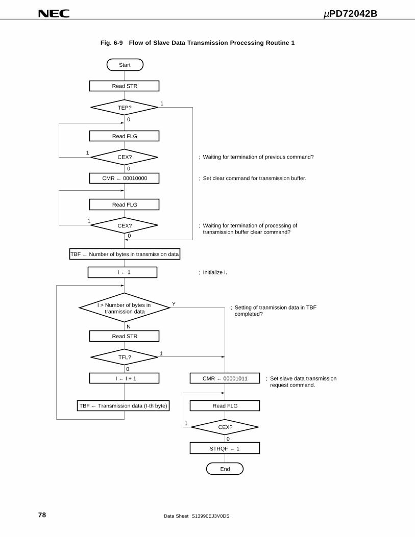
µPD72042B
78 Data Sheet S13990EJ3V0DS
Fig. 6-9 Flow of Slave Data Transmission Processing Routine 1
1
0
0
1
Y
N
0
1
0
1
0
1
Start
Read STR
TEP?
Read FLG
CEX?
CMR ← 00010000
CEX?
Read FLG
TBF ← Number of bytes in transmission data
I ← 1
Read STR
I > Number of bytes in tranmission data
TFL?
I ← I + 1
TBF ← Transmission data (I-th byte)
CMR ← 00001011
Read FLG
End
CEX?
STRQF ← 1
; Set slave data transmission request command.
; Setting of tranmission data in TBF completed?
; Initialize I.
; Waiting for termination of processing of transmission buffer clear command?
; Set clear command for transmission buffer.
; Waiting for termination of previous command?
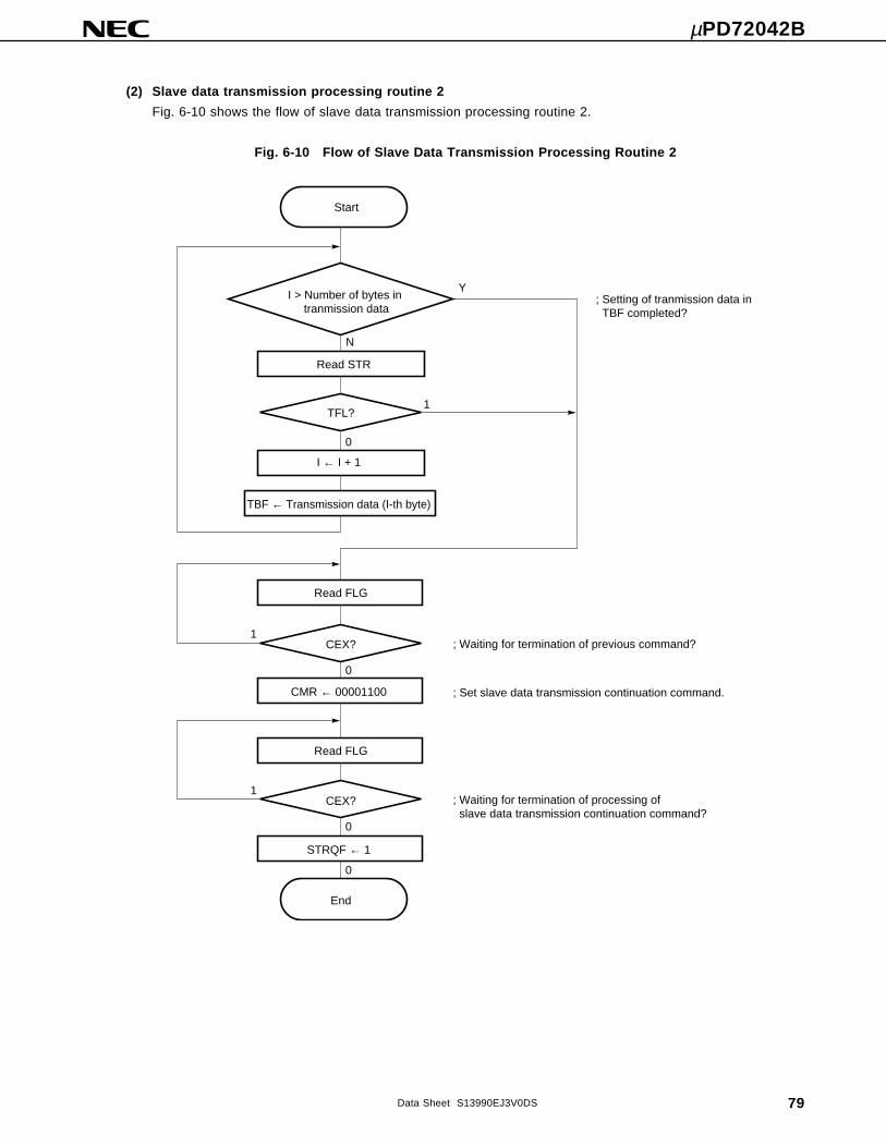
µPD72042B
79Data Sheet S13990EJ3V0DS
(2) Slave data transmission processing routine 2
Fig. 6-10 shows the flow of slave data transmission processing routine 2.
Fig. 6-10 Flow of Slave Data Transmission Processing Routine 2
CMR ← 00001100
Y
N
0
1
0
1
0
1
Start
I > Number of bytes in tranmission data
Read STR
TFL?
I ← I + 1
TBF ← Transmission data (I-th byte)
CEX?
Read FLG
CEX?
Read FLG
STRQF ← 1
End
;
; Set slave data transmission continuation command.
; Waiting for termination of previous command?
;
0
Waiting for termination of processing of slave data transmission continuation command?
Setting of tranmission data in TBF completed?
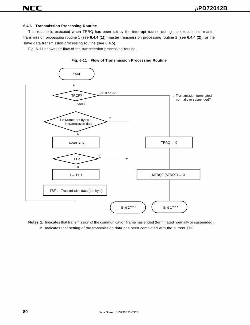
µPD72042B
80 Data Sheet S13990EJ3V0DS
6.4.6 Transmission Processing Routine
This routine is executed when TRRQ has been set by the interrupt routine during the execution of master
transmission processing routine 1 (see 6.4.4 (1)), master transmission processing routine 2 (see 6.4.4 (2)), or the
slave data transmission processing routine (see 6.4.5).
Fig. 6-11 shows the flow of the transmission processing routine.
Fig. 6-11 Flow of Transmission Processing Routine
Notes 1. Indicates that transmission of the communication frame has ended (terminated normally or suspended).
2. Indicates that setting of the transmission data has been completed with the current TBF.
Y
N
0
1
××10 or ××11
××00
Start
TRCF?
Read STR
TFL?
I ← I + 1
TBF ← Transmission data (I-th byte)
End 1Note 1End 2Note 2
MTRQF (STRQF) ← 0
TRRQ ← 0
; Transmission terminated normally or suspended?
I > Number of bytes in tranmission data
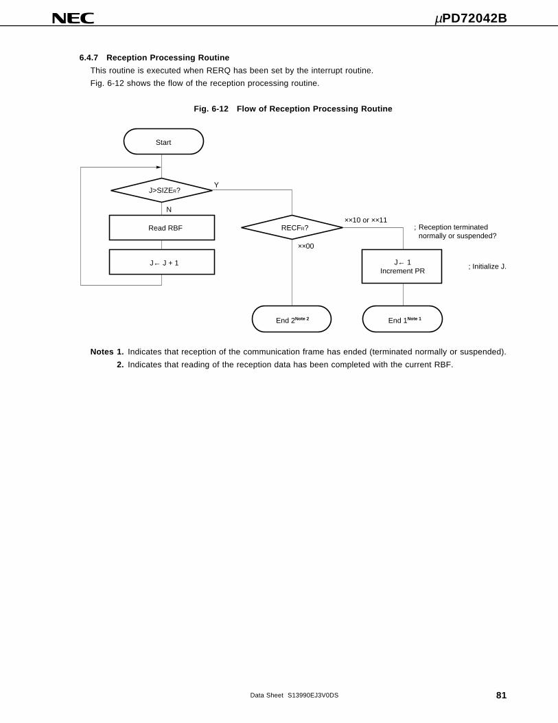
µPD72042B
81Data Sheet S13990EJ3V0DS
6.4.7 Reception Processing Routine
This routine is executed when RERQ has been set by the interrupt routine.
Fig. 6-12 shows the flow of the reception processing routine.
Fig. 6-12 Flow of Reception Processing Routine
Y
N
××00
××10 or ××11
Start
Read RBF
J>SIZER?
J← J + 1
RECFR?
End 2Note 2 End 1Note 1
; Initialize J.
; Reception terminated normally or suspended?
J← 1Increment PR
Notes 1. Indicates that reception of the communication frame has ended (terminated normally or suspended).
2. Indicates that reading of the reception data has been completed with the current RBF.

µPD72042B
82 Data Sheet S13990EJ3V0DS
7. ELECTRICAL CHARACTERISTICS
ABSOLUTE MAXIMUM RATINGS (TA = 25 °C)
Parameter Symbol Conditions Rated value Unit
Supply voltage VDD, AVDD | VDD – AVDD | < 0.5 V –0.5 to +7.0 V
Input voltage for logic section VI –0.5 to VDD + 0.3 V
Output voltage for logic section VO –0.5 to VDD + 0.3 V
Bus input voltage VBI –0.5 to +6.0 V
Bus output voltage VBO –0.5 to +6.0 V
Operating ambient temperature TA –40 to +85 °C
Storage temperature TSTG –65 to +150 °C
Caution Absolute maximum ratings are rated values beyond which physical damage may be caused to
the unit; if any of the parameters in the table above exceeds its rated value, even momentarily,
the performance and/or reliability of the product may deteriorate. Therefore, never exceed the
product’s rated values.
DC CHARACTERISTICS (TA = –40 to +85 °C, VDD = 5 V ±10 %)
Parameter Symbol Conditions Min. Typ. Max. Unit
Input high voltage VIH 0.8VDD VDD V
Input low voltage VIL 0 0.2VDD V
Output high voltage VOH IOH = –400 µA 0.9VDD V
Output low voltage VOL IOL = 2.5 mA 0.4 V
Input leakage current, high ILIH VI = VDD 10 µA
Input leakage current, low ILIL VI = 0 V –10 µA
Output leakage current, high ILOH VO = VDD 10 µA
Output leakage current, low ILOL VO = 0 V –10 µA
Supply current (normal IDD1 3.5 10 mA
operation mode)
Supply current (standby mode) IDD2 50 µA
CAPACITANCE CHARACTERISTICS (TA = 25 °C, VDD = 0 V)
Parameter Symbol Conditions Min. Typ. Max. Unit
Input capacitance CI 15 pF
I/O capacitance CIO 15 pF
fC = 1 MHzExcluding the BUS+ and BUS-pins.0 V for pins others than themeasured pins.
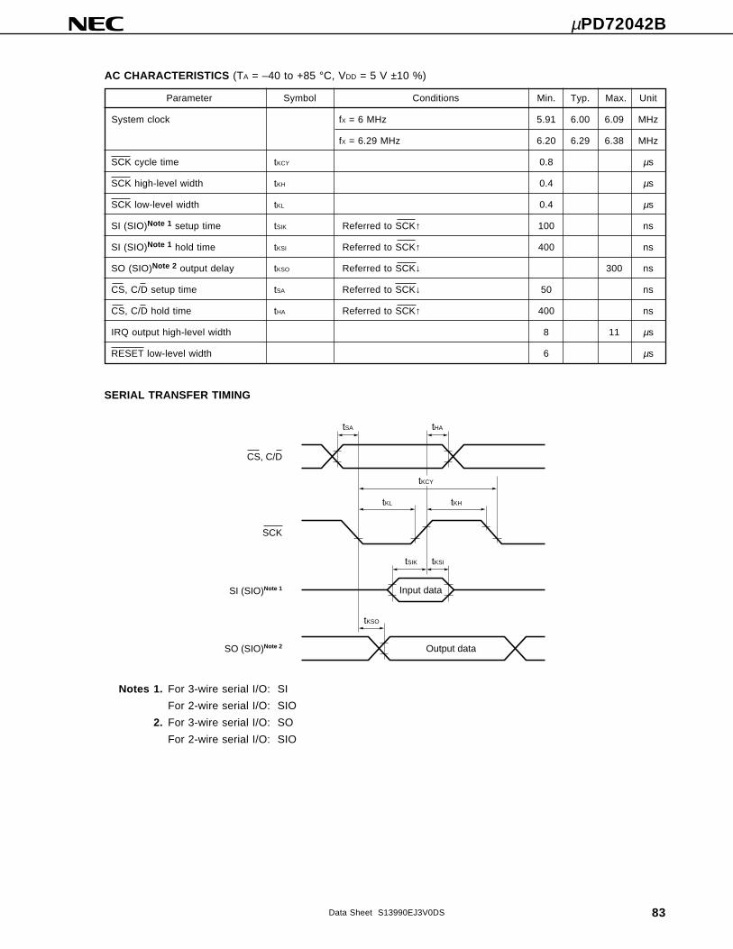
µPD72042B
83Data Sheet S13990EJ3V0DS
AC CHARACTERISTICS (TA = –40 to +85 °C, VDD = 5 V ±10 %)
Parameter Symbol Conditions Min. Typ. Max. Unit
System clock fX = 6 MHz 5.91 6.00 6.09 MHz
fX = 6.29 MHz 6.20 6.29 6.38 MHz
SCK cycle time tKCY 0.8 µs
SCK high-level width tKH 0.4 µs
SCK low-level width tKL 0.4 µs
SI (SIO)Note 1 setup time tSIK Referred to SCK↑ 100 ns
SI (SIO)Note 1 hold time tKSI Referred to SCK↑ 400 ns
SO (SIO)Note 2 output delay tKSO Referred to SCK↓ 300 ns
CS, C/D setup time tSA Referred to SCK↓ 50 ns
CS, C/D hold time tHA Referred to SCK↑ 400 ns
IRQ output high-level width 8 11 µs
RESET low-level width 6 µs
SERIAL TRANSFER TIMING
tSA tHA
tKCY
tKL tKH
tKSItSIK
tKSO
CS, C/D
SCK
SI (SIO)Note 1
SO (SIO)Note 2
Input data
Output data
Notes 1. For 3-wire serial I/O: SI
For 2-wire serial I/O: SIO
2. For 3-wire serial I/O: SO
For 2-wire serial I/O: SIO
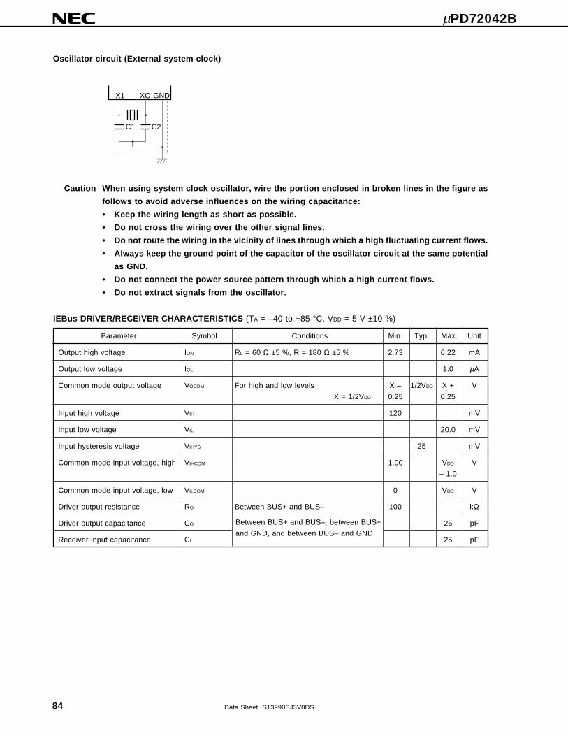
µPD72042B
84 Data Sheet S13990EJ3V0DS
Oscillator circuit (External system clock)
Caution When using system clock oscillator, wire the portion enclosed in broken lines in the figure as
follows to avoid adverse influences on the wiring capacitance:
• Keep the wiring length as short as possible.
• Do not cross the wiring over the other signal lines.
• Do not route the wiring in the vicinity of lines through which a high fluctuating current flows.
• Always keep the ground point of the capacitor of the oscillator circuit at the same potential
as GND.
• Do not connect the power source pattern through which a high current flows.
• Do not extract signals from the oscillator.
IEBus DRIVER/RECEIVER CHARACTERISTICS (TA = –40 to +85 °C, VDD = 5 V ±10 %)
Parameter Symbol Conditions Min. Typ. Max. Unit
Output high voltage ION RL = 60 Ω ±5 %, R = 180 Ω ±5 % 2.73 6.22 mA
Output low voltage IOL 1.0 µA
Common mode output voltage VOCOM For high and low levels X – 1/2VDD X + V
X = 1/2VDD 0.25 0.25
Input high voltage VIH 120 mV
Input low voltage VIL 20.0 mV
Input hysteresis voltage VIHYS 25 mV
Common mode input voltage, high VIHCOM 1.00 VDD V
– 1.0
Common mode input voltage, low VILCOM 0 VDD V
Driver output resistance RO Between BUS+ and BUS– 100 kΩ
Driver output capacitance CO 25 pF
Receiver input capacitance CI 25 pF
Between BUS+ and BUS–, between BUS+
and GND, and between BUS– and GND
X1 XO
C1 C2
GND
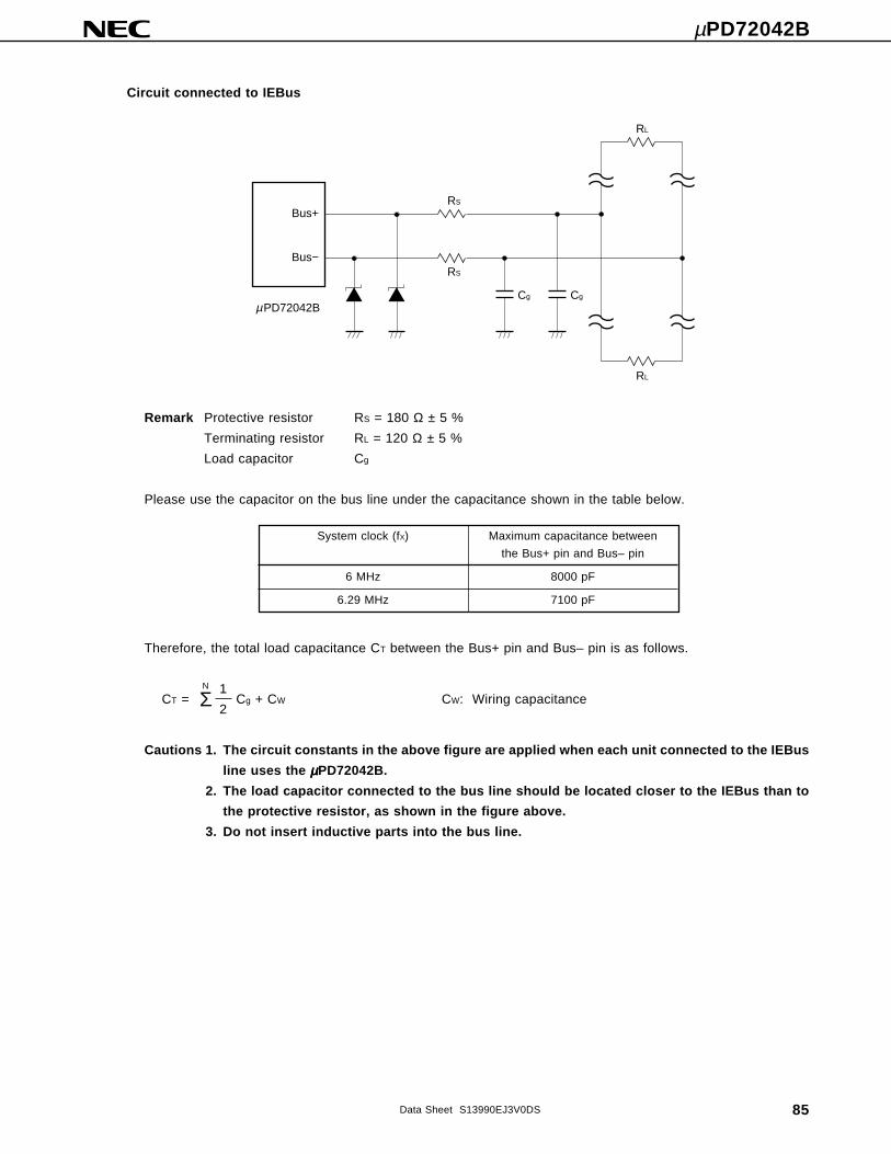
µPD72042B
85Data Sheet S13990EJ3V0DS
Circuit connected to IEBus
Remark Protective resistor RS = 180 Ω ± 5 %
Terminating resistor RL = 120 Ω ± 5 %
Load capacitor Cg
Please use the capacitor on the bus line under the capacitance shown in the table below.
System clock (fX) Maximum capacitance between
the Bus+ pin and Bus– pin
6 MHz 8000 pF
6.29 MHz 7100 pF
Therefore, the total load capacitance CT between the Bus+ pin and Bus– pin is as follows.
CT =N 1
Cg + CW CW: Wiring capacitanceΣ 2
Cautions 1. The circuit constants in the above figure are applied when each unit connected to the IEBus
line uses the µµµµµPD72042B.
2. The load capacitor connected to the bus line should be located closer to the IEBus than to
the protective resistor, as shown in the figure above.
3. Do not insert inductive parts into the bus line.
Bus+RS
RS
Cg Cg
RL
RL
Bus−
µPD72042B
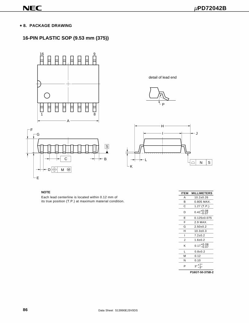
µPD72042B
86 Data Sheet S13990EJ3V0DS
8. PACKAGE DRAWING
NOTE
Each lead centerline is located within 0.12 mm ofits true position (T.P.) at maximum material condition.
A
BN
E
detail of lead end
K
L
P
H
GF
I
D
1 8
16 9
M
S
S
C
M
J
16-PIN PLASTIC SOP (9.53 mm (375))
ITEM
B
C
I
A
D
E
F
G
H
J
M
MILLIMETERS
1.27 (T.P.)
0.805 MAX.
7.2±0.2
10.2±0.26
0.125±0.075
0.42
2.9 MAX.
10.3±0.3
2.50±0.2
+0.08−0.07
1.6±0.2
0.12
0.10N
K
L
0.17+0.08−0.07
0.8±0.2
P 3°+7°−3°
P16GT-50-375B-2
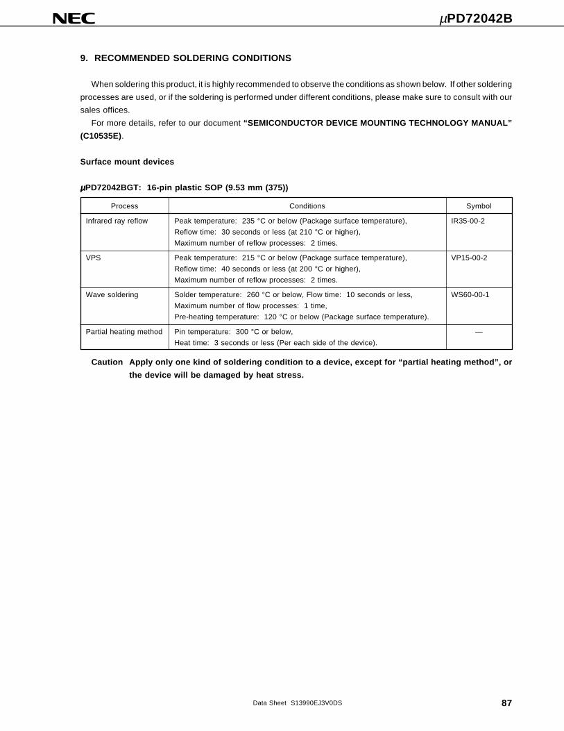
µPD72042B
87Data Sheet S13990EJ3V0DS
9. RECOMMENDED SOLDERING CONDITIONS
When soldering this product, it is highly recommended to observe the conditions as shown below. If other soldering
processes are used, or if the soldering is performed under different conditions, please make sure to consult with our
sales offices.
For more details, refer to our document “SEMICONDUCTOR DEVICE MOUNTING TECHNOLOGY MANUAL”
(C10535E).
Surface mount devices
µµµµµPD72042BGT: 16-pin plastic SOP (9.53 mm (375))
Process Conditions Symbol
Infrared ray reflow Peak temperature: 235 °C or below (Package surface temperature), IR35-00-2
Reflow time: 30 seconds or less (at 210 °C or higher),
Maximum number of reflow processes: 2 times.
VPS Peak temperature: 215 °C or below (Package surface temperature), VP15-00-2
Reflow time: 40 seconds or less (at 200 °C or higher),
Maximum number of reflow processes: 2 times.
Wave soldering Solder temperature: 260 °C or below, Flow time: 10 seconds or less, WS60-00-1
Maximum number of flow processes: 1 time,
Pre-heating temperature: 120 °C or below (Package surface temperature).
Partial heating method Pin temperature: 300 °C or below, —
Heat time: 3 seconds or less (Per each side of the device).
Caution Apply only one kind of soldering condition to a device, except for “partial heating method”, or
the device will be damaged by heat stress.
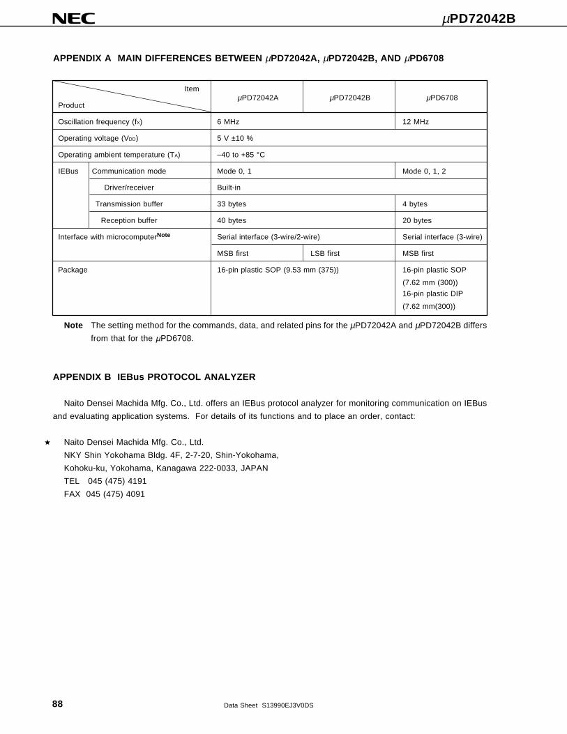
µPD72042B
88 Data Sheet S13990EJ3V0DS
APPENDIX A MAIN DIFFERENCES BETWEEN µPD72042A, µPD72042B, AND µPD6708
ItemµPD72042A µPD72042B µPD6708
Product
Oscillation frequency (fX) 6 MHz 12 MHz
Operating voltage (VDD) 5 V ±10 %
Operating ambient temperature (TA) –40 to +85 °C
IEBus Communication mode Mode 0, 1 Mode 0, 1, 2
Driver/receiver Built-in
Transmission buffer 33 bytes 4 bytes
Reception buffer 40 bytes 20 bytes
Interface with microcomputerNote Serial interface (3-wire/2-wire) Serial interface (3-wire)
MSB first LSB first MSB first
Package 16-pin plastic SOP (9.53 mm (375)) 16-pin plastic SOP
(7.62 mm (300))
16-pin plastic DIP
(7.62 mm(300))
Note The setting method for the commands, data, and related pins for the µPD72042A and µPD72042B differs
from that for the µPD6708.
APPENDIX B IEBus PROTOCOL ANALYZER
Naito Densei Machida Mfg. Co., Ltd. offers an IEBus protocol analyzer for monitoring communication on IEBus
and evaluating application systems. For details of its functions and to place an order, contact:
Naito Densei Machida Mfg. Co., Ltd.
NKY Shin Yokohama Bldg. 4F, 2-7-20, Shin-Yokohama,
Kohoku-ku, Yokohama, Kanagawa 222-0033, JAPAN
TEL 045 (475) 4191
FAX 045 (475) 4091
µPD72042B
89Data Sheet S13990EJ3V0DS
NOTES FOR CMOS DEVICES
1 PRECAUTION AGAINST ESD FOR SEMICONDUCTORS
Note:
Strong electric field, when exposed to a MOS device, can cause destruction of the gate oxide and
ultimately degrade the device operation. Steps must be taken to stop generation of static electricity
as much as possible, and quickly dissipate it once, when it has occurred. Environmental control
must be adequate. When it is dry, humidifier should be used. It is recommended to avoid using
insulators that easily build static electricity. Semiconductor devices must be stored and transported
in an anti-static container, static shielding bag or conductive material. All test and measurement
tools including work bench and floor should be grounded. The operator should be grounded using
wrist strap. Semiconductor devices must not be touched with bare hands. Similar precautions need
to be taken for PW boards with semiconductor devices on it.
2 HANDLING OF UNUSED INPUT PINS FOR CMOS
Note:
No connection for CMOS device inputs can be cause of malfunction. If no connection is provided
to the input pins, it is possible that an internal input level may be generated due to noise, etc., hence
causing malfunction. CMOS devices behave differently than Bipolar or NMOS devices. Input levels
of CMOS devices must be fixed high or low by using a pull-up or pull-down circuitry. Each unused
pin should be connected to VDD or GND with a resistor, if it is considered to have a possibility of
being an output pin. All handling related to the unused pins must be judged device by device and
related specifications governing the devices.
3 STATUS BEFORE INITIALIZATION OF MOS DEVICES
Note:
Power-on does not necessarily define initial status of MOS device. Production process of MOS
does not define the initial operation status of the device. Immediately after the power source is
turned ON, the devices with reset function have not yet been initialized. Hence, power-on does
not guarantee out-pin levels, I/O settings or contents of registers. Device is not initialized until the
reset signal is received. Reset operation must be executed immediately after power-on for devices
having reset function.

µPD72042B
IEBus and Inter Equipment are trademarks of NEC Corporation.
M8E 00. 4
The information in this document is current as of July, 2002. The information is subject to change without notice. For actual design-in, refer to the latest publications of NEC's data sheets or data books, etc., for the most up-to-date specifications of NEC semiconductor products. Not all products and/or types are available in every country. Please check with an NEC sales representative for availability and additional information.No part of this document may be copied or reproduced in any form or by any means without prior written consent of NEC. NEC assumes no responsibility for any errors that may appear in this document.NEC does not assume any liability for infringement of patents, copyrights or other intellectual property rights of third parties by or arising from the use of NEC semiconductor products listed in this document or any other liability arising from the use of such products. No license, express, implied or otherwise, is granted under any patents, copyrights or other intellectual property rights of NEC or others.Descriptions of circuits, software and other related information in this document are provided for illustrative purposes in semiconductor product operation and application examples. The incorporation of these circuits, software and information in the design of customer's equipment shall be done under the full responsibility of customer. NEC assumes no responsibility for any losses incurred by customers or third parties arising from the use of these circuits, software and information.While NEC endeavours to enhance the quality, reliability and safety of NEC semiconductor products, customers agree and acknowledge that the possibility of defects thereof cannot be eliminated entirely. To minimize risks of damage to property or injury (including death) to persons arising from defects in NEC semiconductor products, customers must incorporate sufficient safety measures in their design, such as redundancy, fire-containment, and anti-failure features.NEC semiconductor products are classified into the following three quality grades:"Standard", "Special" and "Specific". The "Specific" quality grade applies only to semiconductor products developed based on a customer-designated "quality assurance program" for a specific application. The recommended applications of a semiconductor product depend on its quality grade, as indicated below. Customers must check the quality grade of each semiconductor product before using it in a particular application. "Standard": Computers, office equipment, communications equipment, test and measurement equipment, audio
and visual equipment, home electronic appliances, machine tools, personal electronic equipmentand industrial robots
"Special": Transportation equipment (automobiles, trains, ships, etc.), traffic control systems, anti-disastersystems, anti-crime systems, safety equipment and medical equipment (not specifically designedfor life support)
"Specific": Aircraft, aerospace equipment, submersible repeaters, nuclear reactor control systems, lifesupport systems and medical equipment for life support, etc.
The quality grade of NEC semiconductor products is "Standard" unless otherwise expressly specified in NEC's data sheets or data books, etc. If customers wish to use NEC semiconductor products in applications not intended by NEC, they must contact an NEC sales representative in advance to determine NEC's willingness to support a given application.(Note)(1) "NEC" as used in this statement means NEC Corporation and also includes its majority-owned subsidiaries.(2) "NEC semiconductor products" means any semiconductor product developed or manufactured by or forNEC (as defined above).
•
•
•
•
•
•