Embed Size (px)
Citation preview
7/27/2019 MOS Smaple and Hold Amplifiers
http://slidepdf.com/reader/full/mos-smaple-and-hold-amplifiers 1/30
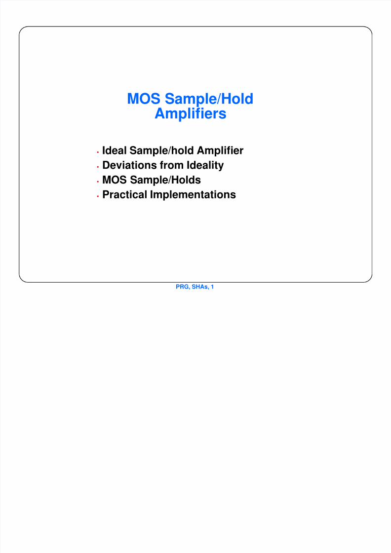
PRG, SHAs, 1
MOS Sample/HoldAmplifiers
• Ideal Sample/hold Amplifier
•Deviations from Ideality
•MOS Sample/Holds
•Practical Implementations

7/27/2019 MOS Smaple and Hold Amplifiers
http://slidepdf.com/reader/full/mos-smaple-and-hold-amplifiers 2/30
Ideal Sample/Hold
vi
T/H
T/Hout
S/H
out
t
t
t
t
S/Hvi
T/H in
inT
H
T
Vout

7/27/2019 MOS Smaple and Hold Amplifiers
http://slidepdf.com/reader/full/mos-smaple-and-hold-amplifiers 3/30
1. Hold to Track Transition
vi
T/H
t
in
S/Hvi
T/H
vo
Finite acquisition time
2. Track Mode
DC offset
Finite Bandwidth3. Track-Hold Transition
S/H OffsetAperture Delay
H
T
H
Important Deviations from Ideality
T

7/27/2019 MOS Smaple and Hold Amplifiers
http://slidepdf.com/reader/full/mos-smaple-and-hold-amplifiers 4/30
PRG, SHAs, 4
Performance Limits in SHAs:What Ultimately Limits Performance in A/D InterfaceSystems?
•Fundamental Device limitations in SH function
•Practical Design Issues in SH function
Can We Do this?:
AntennaLPF S/H ADC
All-DigitalTV
500Mhz,18bitADC
Key Issue: For a given technology, what limitssampling bandwidth and rate?

7/27/2019 MOS Smaple and Hold Amplifiers
http://slidepdf.com/reader/full/mos-smaple-and-hold-amplifiers 5/30
f sig f s
f sig f s
f sig f s f sig f s
f sig f s
f sig f s
Ideal S/H
Real S/H
Sample
Sample
Sample
Beat Freq Test
A Frequency Domain View
Distortion Productsplus noise
Sources of Noise:
Sources of Distortion:
Jitter, kT/C

7/27/2019 MOS Smaple and Hold Amplifiers
http://slidepdf.com/reader/full/mos-smaple-and-hold-amplifiers 6/30
PRG, SHAs, 6
The Sampling Jitter Problem
Assume Nyquist Sampling at fs = 2 f sig
Result:
δV
V
π
2
∆t
Ts
≈
Key Point: For Nyquist sampling, need:
RMS Jitter <
1
6
1
2B
Ts
δV
dV
dt ∆t 2πVf= =

7/27/2019 MOS Smaple and Hold Amplifiers
http://slidepdf.com/reader/full/mos-smaple-and-hold-amplifiers 7/30
PRG, SHAs, 7
Jitter Requirements at VariousSampling Rates
SR 8 bits 10 bits 12 bits
1 MHz 700ps 175ps 44ps
10MHz 70ps 17.5ps 4.4ps
100MHz 7ps 1.75ps 0.44ps
1GHz 0.7ps 0.175ps 0.044ps

7/27/2019 MOS Smaple and Hold Amplifiers
http://slidepdf.com/reader/full/mos-smaple-and-hold-amplifiers 8/30
PRG, SHAs, 8
0 dB-70dB
10
20
30
40
50
60
7080
90
S/(N+D)
Input level
Low frequency signal
High Frequency Signal
V̇o Vos Vin 1 ε1
+( ) ε2
dVin
dt
ε3
dVin
dt
2
higherterms+ + + +=

7/27/2019 MOS Smaple and Hold Amplifiers
http://slidepdf.com/reader/full/mos-smaple-and-hold-amplifiers 9/30
PRG, SHAs, 9
Vin
Vg
Cs
Vo
MOS Sample/Hold Circuits
Fundamental Limits to Performance• kT/C Noise
• Sampling Jitter
• Sample-Mode Bandwidth
Practical Limits to Performance
• Charge-injection errors

7/27/2019 MOS Smaple and Hold Amplifiers
http://slidepdf.com/reader/full/mos-smaple-and-hold-amplifiers 10/30
PRG, SHAs, 10
C
100pF 6.4uV
10pF 21uV
1pF 64uV
100fF 210uV
10fF 0.64mV
kTC
kT/C Noise Limitation
VinCs
Vov
n2
4kTR∆f=
vo
2
f
vo
2
vo
2
∫ df kT
C=
V
Variance=kT/C
Vsample
Probability

7/27/2019 MOS Smaple and Hold Amplifiers
http://slidepdf.com/reader/full/mos-smaple-and-hold-amplifiers 11/30
PRG, SHAs, 11
Another Interpretation:
Vin Cs
Vo
εn
E 12
CV2
kT ExpectedNoiseEnergy= = =
SNRεsigkT
=
εsig SignalEnergy
1
2CV
2
sig= =

7/27/2019 MOS Smaple and Hold Amplifiers
http://slidepdf.com/reader/full/mos-smaple-and-hold-amplifiers 12/30
PRG, SHAs, 12
Sample/Hold Offset
Vin
Vg
Cs
Vo
Vg
t
(vin+VT)
vin
VoVin
vin
∆v−( )+
What’s happening in the device?
S
G
D
Sub
Limiting Case1: Slow gate fall time, channel equilibrates
Limiting Case 2: Fast gate fall time, 1/2 of qc goes each way
S D
G
Substrate

7/27/2019 MOS Smaple and Hold Amplifiers
http://slidepdf.com/reader/full/mos-smaple-and-hold-amplifiers 13/30
PRG, SHAs, 13
Fast Case
S
G
D
Sub
Vg
Vg
t
φs
x
Lt=0-
φs x
L
t=0+
φs x
Lt=0++
Vg
id,is
Vout
t
t
t
isid
dV
Vout

7/27/2019 MOS Smaple and Hold Amplifiers
http://slidepdf.com/reader/full/mos-smaple-and-hold-amplifiers 14/30
PRG, SHAs, 14
Fast Case, Cont.
∆VColC
L
VH
VL
− −
12
L 2Ld−
WLCox VH VT
− Vi−
CL
−=
∆V Vi
1 ε+( ) Vos
+=
Vos
COL
CL
V(H
VL
)−12
V(H
− VL
)C
C−=
ε 12
W L 2D ) Cox
−
CL
=
Where:
C2 Cox L 2Ld−
W=
∆VC
olC
L
VH
VL
− −
12
qchannel
CL
−=
7/27/2019 MOS Smaple and Hold Amplifiers
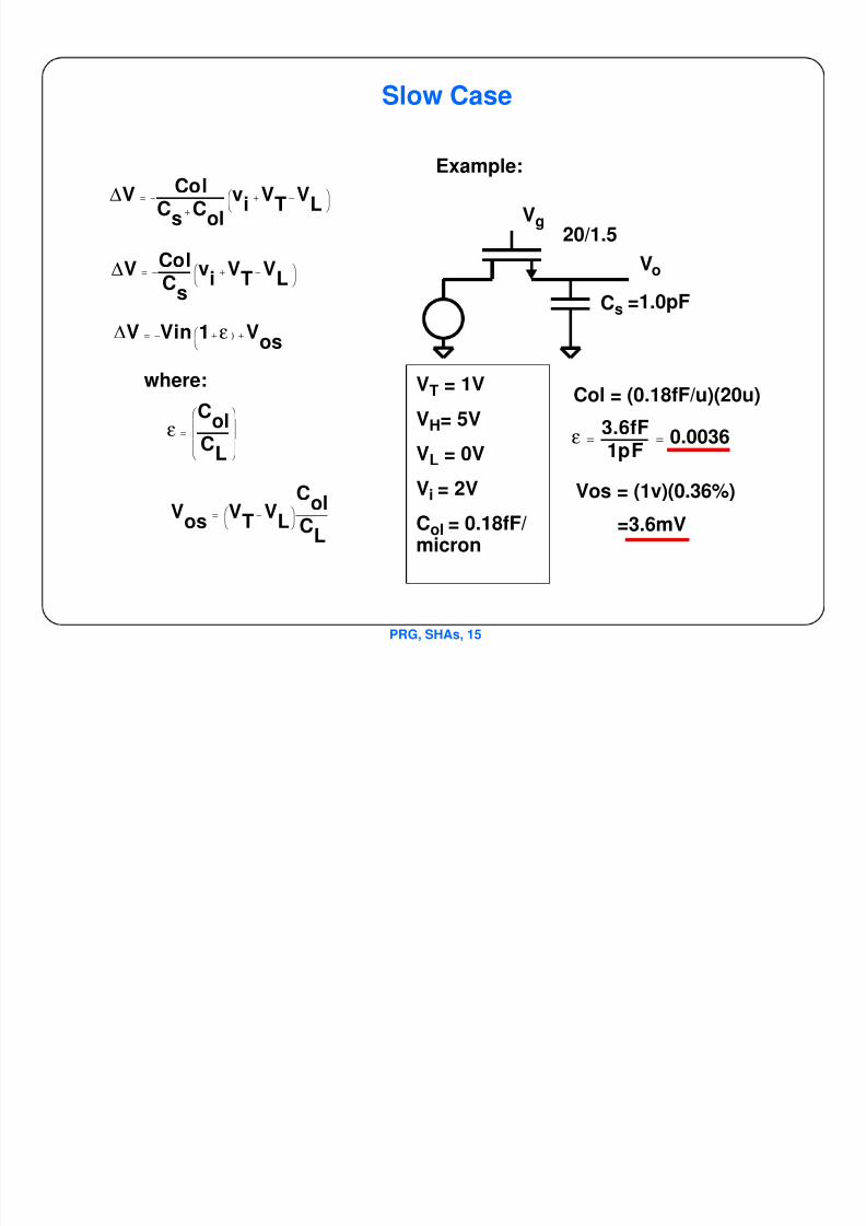
http://slidepdf.com/reader/full/mos-smaple-and-hold-amplifiers 15/30
PRG, SHAs, 15
Slow Case
Vg
Cs
Vo
20/1.5
=1.0pF
∆V ColC
sC
ol+
vi
VT
VL
−+−=
ε 3.6fF1pF
0.0036= =
∆V ColC
s
vi
VT
VL
−+−=
∆V Vin 1 ε ) Vos
+ + −=
εC
olC
L
=
where:
Vos
VT
VL
−
Col
CL
=
Example:
VT = 1V
VH= 5V
VL = 0V
Vi = 2V
Col = 0.18fF/micron
Col = (0.18fF/u)(20u)
Vos = (1v)(0.36%)
=3.6mV

7/27/2019 MOS Smaple and Hold Amplifiers
http://slidepdf.com/reader/full/mos-smaple-and-hold-amplifiers 16/30
PRG, SHAs, 16
Fast Case Example
Vin=1V
VT = 1V
VH = 5V
VL = 0VVi = 2V
Col = 0.18fF/micron
Cox = 1ff/square micron
Result:
ε 12
20µ 1.14µ( )1ff
µ2
1pF0.014= =
Vos = 6.3mV
0.014
0.0036
fast slow
ε
6.3mV
3.6mV
fast slow
Vos
Vg
Cs
Vo
20/1.5
=1.0pF
Refs:
Wilson,JSC,12/85
Shieh, JSC, 4/87Vittoz, JSC, 6/85
β µCox
WL
=
VH
VL
−( ) βUC
s
UdV
gdt
=
Critical params:
7/27/2019 MOS Smaple and Hold Amplifiers
http://slidepdf.com/reader/full/mos-smaple-and-hold-amplifiers 17/30
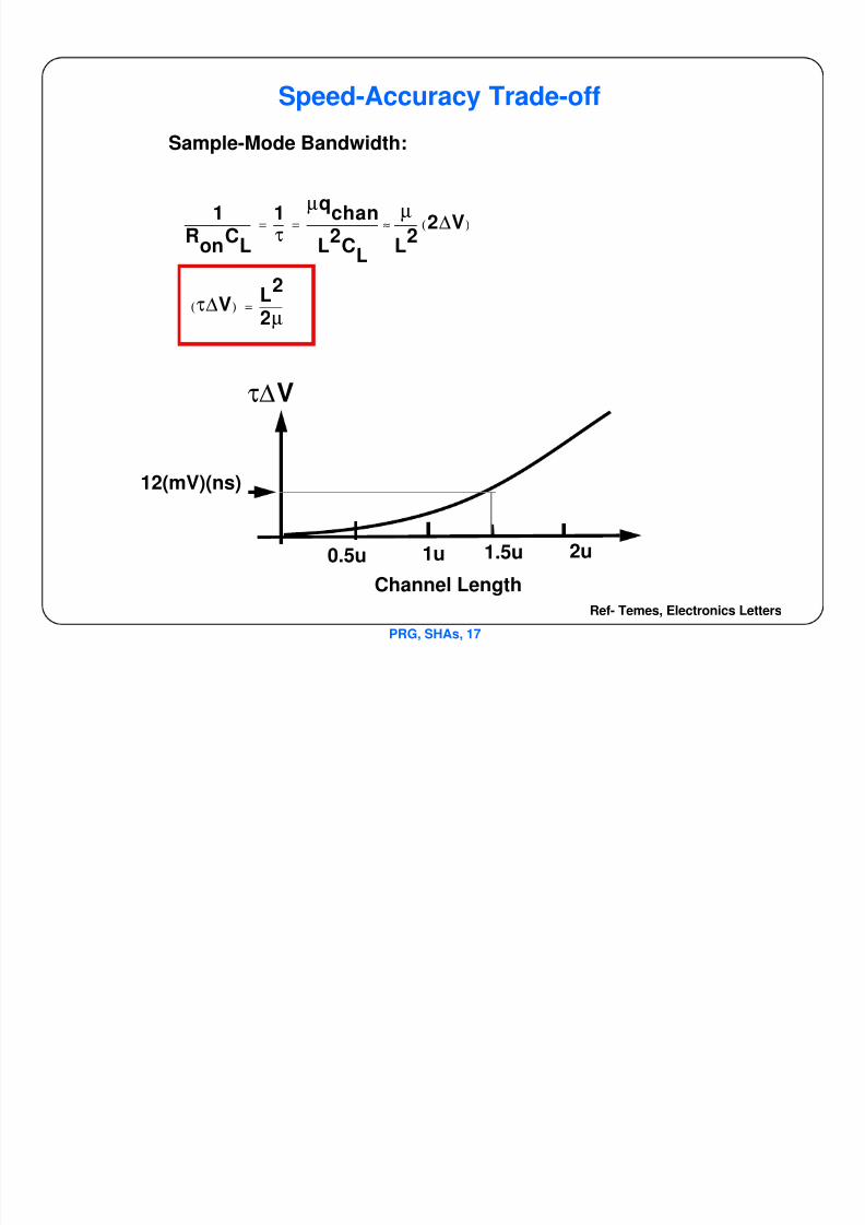
PRG, SHAs, 17
Speed-Accuracy Trade-off
Sample-Mode Bandwidth:
τ∆V( )L
2
2µ=
1
RonCL
1
τ
µqchan
L2CL
µ
L22∆V( )≈= =
τ∆V
0.5u 1u 1.5u 2u
Channel Length
12(mV)(ns)
Ref- Temes, Electronics Letters

7/27/2019 MOS Smaple and Hold Amplifiers
http://slidepdf.com/reader/full/mos-smaple-and-hold-amplifiers 18/30
PRG, SHAs, 18
Practical Implementations of CMOS SHAs
Key Issue: Control of Charge Injection
1. Dummy Switch
Cs
Problem: No way to balance overClock fall time variations
2. Dummy Switch w/Charge Balance Cap
Cs
Problem: R must be big,
limits sample-mode bandwidth

7/27/2019 MOS Smaple and Hold Amplifiers
http://slidepdf.com/reader/full/mos-smaple-and-hold-amplifiers 19/30
PRG, SHAs, 19
Implementations, Cont’d
3. Complementary NMOS, PMOS
Cs
Vh
Vl
t
Assume fast case12
qCN
12
VH
VTN
Vi
−−( ) WN
LN
CoxN
= Key Point:
1. Offsets PartiallyCancel
2. Gain errors ADD!!
1
2
q
CP
1
2
V
i
V
TP
V
L
−−( ) W
P
L
P
C
oxP
=
∆V Vin 1 ε ) Vos
+ + −=
εW
PL
PC
oxPW
NL
NC
oxN+
CL
=
where:
Vos
VOSN
VOSP
−
Col
CL
=
,

7/27/2019 MOS Smaple and Hold Amplifiers
http://slidepdf.com/reader/full/mos-smaple-and-hold-amplifiers 20/30
PRG, SHAs, 20
Implementations, Cont’d
4. Get rid of offset- Go Differential
Cs
Cs
vi+
vi-
Vg
Vo+
Vo-
vo1
vi1
1 ε+( ) Vos1
+=
v
o2
v
i2
1 ε+( ) V
os2
+=
∆vo
∆vi
1 ε+( )=

7/27/2019 MOS Smaple and Hold Amplifiers
http://slidepdf.com/reader/full/mos-smaple-and-hold-amplifiers 21/30
PRG, SHAs, 21
Implementations, Cont’d
4. Get rid of Signal-Dependent Error- Bottom Plate Sampling
Csvi
+
vi-
Vo+
Vo-
Cs
φ1
φ2
1. Turn off
2. Turn off
3. Use Active Ckt to sense
φ2
φ1
φ1
φ2

7/27/2019 MOS Smaple and Hold Amplifiers
http://slidepdf.com/reader/full/mos-smaple-and-hold-amplifiers 22/30
PRG, SHAs, 22
Implementations, Cont’d
6. Add active device for signal sensing
Csvi+
vi- Cs
φ1A
φ1
φ1B
φ2
φ1C
φ1
φ2
φ2
AZ
vo+
vo-
φ1A
φ1B
φ1C
φ2
Example:
Ohara JSC 12/87
Vos<100uV
S/M BW = 30Mhz
Nulling Switch gives 4x better figure of merit

7/27/2019 MOS Smaple and Hold Amplifiers
http://slidepdf.com/reader/full/mos-smaple-and-hold-amplifiers 23/30
PRG, SHAs, 23
Stand-Alone Building-Block SHAs
Important Characteristic:
• Low-Impedance NRZ Output
• Usually Bipolar or BICMOS
Common Configurations:
Open Loop:
Closed Loop:
Closed Loop withSumming NodeSampling
refs: Chambers ISSCC91,Real, ISSCC91, Wooley ISSCC90

7/27/2019 MOS Smaple and Hold Amplifiers
http://slidepdf.com/reader/full/mos-smaple-and-hold-amplifiers 24/30
PRG, SHAs, 24
Stand-Alone SHAs, Cont’d
Example: Wooley JSC 12-89, Stafford JSC 12/74
-
+
-
+vin
S/H
CLRL
• Bottom-Plate Sampling- Different Implementation
• Output amp always active and valid
• Widely used in building blocks
• Disadvantage- Sample Mode Bandwidth limited by active devices
• Disadvantage- Offset, Noise limited by Amps

7/27/2019 MOS Smaple and Hold Amplifiers
http://slidepdf.com/reader/full/mos-smaple-and-hold-amplifiers 25/30
PRG, SHAs, 25
Nonlinear Transient Charge Injection in
MOS SHAs
Csvi
+
vi-
Vo+
Vo-
Cs
φ2
Ron1
Ron2
i=C(dV/dT)
i=C(dV/dT)
+
-
vds
= Ron
C(dv/dt)
v
ds
= -R
on
C(dv/dt)
+
-
Two Key Effects:
1. Ron
1, Ron
2 = f(vin
). Creates
Must match Ron
s
Signal-dependent charge-inj.
2. vds differences at turnoff givesdv/dt dependent charge
injection mismatch.
Must optimize switch sizes
Ref: Lin, JSC, April 91

7/27/2019 MOS Smaple and Hold Amplifiers
http://slidepdf.com/reader/full/mos-smaple-and-hold-amplifiers 26/30
PRG, SHAs, 26
Summary of S/H Charge-Injection Errors
Error Term Ckt Techniques
Vos Differential S/H
AZ Amplifier
Bottom-platesampler
Limits S/M Band-width
Nonlinear Chg Inj.
Vε Vos ε1Vin+ ε2
dVin
dt
ε3
dVin
dt
2
etc+ += =
ε1
ε2
ε3

7/27/2019 MOS Smaple and Hold Amplifiers
http://slidepdf.com/reader/full/mos-smaple-and-hold-amplifiers 27/30
PRG, SHAs, 27
Diode Bridge Samplers
vin
Ibias
isw
Ibiasisw
Cs
Vout
t
off
on
t
off
on
isw
• Can be very fast if diodes are fast (i.e. Schottky)
• Hard to control pedestal- currents must match and must clamp toVout
• Matches ECL Bipolar well
•
Best suited to High-speed/low accuracy
Refs- Corcoran, ISSC87

7/27/2019 MOS Smaple and Hold Amplifiers
http://slidepdf.com/reader/full/mos-smaple-and-hold-amplifiers 28/30
PRG, SHAs, 28
Speed-Accuracy Trade-off in Diode Samplers
vin
Ibias
isw
Ibiasisw
Cs
Neglect Parasitics
Ron 1gm
kTqI
d∼=
qstored
Ibias
τf
=
Vεq
storedC
s
Ibias
τf
Cs
= =
ω 3db−1R
onC
s
I
biasC
skTq
1τ= = =
τVε τf kTq
W
b
( )2
2µ= =
τVεL( )
2
2µ=
(Bipolar Figure of Merit)
(MOS Figure of Merit)
Ron
As
7/27/2019 MOS Smaple and Hold Amplifiers
http://slidepdf.com/reader/full/mos-smaple-and-hold-amplifiers 29/30
PRG, SHAs, 29
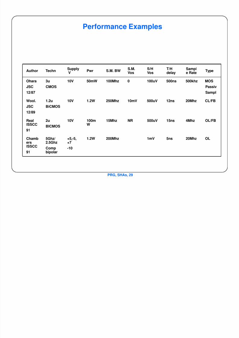
Performance Examples
Author TechnSupplyV
Pwr S.M. BWS.M.Vos
S/HVos
T/Hdelay
Sample Rate
Type
Ohara
JSC
12/87
3u
CMOS
10V 50mW 100Mhz 0 100uV 500ns 500khz MOS
Passiv
Sampl
Wool.
JSC
12/89
1.2u
BiCMOS
10V 1.2W 250Mhz 10mV 500uV 12ns 20Mhz CL/FB
RealISSCC
91
2u
BICMOS
10V 100mW
15Mhz NR 500uV 15ns 4Mhz OL/FB
ChambersISSCC
91
5Ghz/2.5Ghz
Compbipolar
+5,-5,+7
-10
1.2W 200Mhz 1mV 5ns 20Mhz OL
7/27/2019 MOS Smaple and Hold Amplifiers
http://slidepdf.com/reader/full/mos-smaple-and-hold-amplifiers 30/30
PRG, SHAs, 30
References on SHAs
• Stafford, et al JSC 12/74
• Vittoz, et al, JSC, 6/85
• Wilson, et al, JSC, 12/85
• Shieh,et al, JSC, 4/87
• Ohara, et al, JSC, 12/87
• Wooley, et al, JSC, 12/89
• Chambers,et al, ISSCC91
•
Real, et al, ISSCC91• Corcoran, et al, ISSCC87
• Lin JSC 4/91